EP3940751A1 - Spacer structure for semiconductor device and method for forming the same - Google Patents
Spacer structure for semiconductor device and method for forming the same Download PDFInfo
- Publication number
- EP3940751A1 EP3940751A1 EP21185499.7A EP21185499A EP3940751A1 EP 3940751 A1 EP3940751 A1 EP 3940751A1 EP 21185499 A EP21185499 A EP 21185499A EP 3940751 A1 EP3940751 A1 EP 3940751A1
- Authority
- EP
- European Patent Office
- Prior art keywords
- etching process
- etching
- dielectric layer
- layer
- dry etching
- Prior art date
- Legal status (The legal status is an assumption and is not a legal conclusion. Google has not performed a legal analysis and makes no representation as to the accuracy of the status listed.)
- Withdrawn
Links
Images




Classifications
-
- H—ELECTRICITY
- H10—SEMICONDUCTOR DEVICES; ELECTRIC SOLID-STATE DEVICES NOT OTHERWISE PROVIDED FOR
- H10D—INORGANIC ELECTRIC SEMICONDUCTOR DEVICES
- H10D84/00—Integrated devices formed in or on semiconductor substrates that comprise only semiconducting layers, e.g. on Si wafers or on GaAs-on-Si wafers
- H10D84/01—Manufacture or treatment
- H10D84/02—Manufacture or treatment characterised by using material-based technologies
- H10D84/03—Manufacture or treatment characterised by using material-based technologies using Group IV technology, e.g. silicon technology or silicon-carbide [SiC] technology
- H10D84/038—Manufacture or treatment characterised by using material-based technologies using Group IV technology, e.g. silicon technology or silicon-carbide [SiC] technology using silicon technology, e.g. SiGe
-
- H—ELECTRICITY
- H10—SEMICONDUCTOR DEVICES; ELECTRIC SOLID-STATE DEVICES NOT OTHERWISE PROVIDED FOR
- H10D—INORGANIC ELECTRIC SEMICONDUCTOR DEVICES
- H10D62/00—Semiconductor bodies, or regions thereof, of devices having potential barriers
- H10D62/10—Shapes, relative sizes or dispositions of the regions of the semiconductor bodies; Shapes of the semiconductor bodies
- H10D62/113—Isolations within a component, i.e. internal isolations
- H10D62/115—Dielectric isolations, e.g. air gaps
- H10D62/116—Dielectric isolations, e.g. air gaps adjoining the input or output regions of field-effect devices, e.g. adjoining source or drain regions
-
- H—ELECTRICITY
- H10—SEMICONDUCTOR DEVICES; ELECTRIC SOLID-STATE DEVICES NOT OTHERWISE PROVIDED FOR
- H10D—INORGANIC ELECTRIC SEMICONDUCTOR DEVICES
- H10D64/00—Electrodes of devices having potential barriers
- H10D64/01—Manufacture or treatment
- H10D64/021—Manufacture or treatment using multiple gate spacer layers, e.g. bilayered sidewall spacers
-
- H—ELECTRICITY
- H10—SEMICONDUCTOR DEVICES; ELECTRIC SOLID-STATE DEVICES NOT OTHERWISE PROVIDED FOR
- H10D—INORGANIC ELECTRIC SEMICONDUCTOR DEVICES
- H10D30/00—Field-effect transistors [FET]
- H10D30/01—Manufacture or treatment
- H10D30/014—Manufacture or treatment of FETs having zero-dimensional [0D] or one-dimensional [1D] channels, e.g. quantum wire FETs, single-electron transistors [SET] or Coulomb blockade transistors
-
- H—ELECTRICITY
- H10—SEMICONDUCTOR DEVICES; ELECTRIC SOLID-STATE DEVICES NOT OTHERWISE PROVIDED FOR
- H10D—INORGANIC ELECTRIC SEMICONDUCTOR DEVICES
- H10D30/00—Field-effect transistors [FET]
- H10D30/01—Manufacture or treatment
- H10D30/021—Manufacture or treatment of FETs having insulated gates [IGFET]
- H10D30/024—Manufacture or treatment of FETs having insulated gates [IGFET] of fin field-effect transistors [FinFET]
-
- H—ELECTRICITY
- H10—SEMICONDUCTOR DEVICES; ELECTRIC SOLID-STATE DEVICES NOT OTHERWISE PROVIDED FOR
- H10D—INORGANIC ELECTRIC SEMICONDUCTOR DEVICES
- H10D30/00—Field-effect transistors [FET]
- H10D30/40—FETs having zero-dimensional [0D], one-dimensional [1D] or two-dimensional [2D] charge carrier gas channels
- H10D30/43—FETs having zero-dimensional [0D], one-dimensional [1D] or two-dimensional [2D] charge carrier gas channels having one-dimensional [1D] charge carrier gas channels, e.g. quantum wire FETs or transistors having 1D quantum-confined channels
-
- H—ELECTRICITY
- H10—SEMICONDUCTOR DEVICES; ELECTRIC SOLID-STATE DEVICES NOT OTHERWISE PROVIDED FOR
- H10D—INORGANIC ELECTRIC SEMICONDUCTOR DEVICES
- H10D30/00—Field-effect transistors [FET]
- H10D30/60—Insulated-gate field-effect transistors [IGFET]
- H10D30/62—Fin field-effect transistors [FinFET]
-
- H—ELECTRICITY
- H10—SEMICONDUCTOR DEVICES; ELECTRIC SOLID-STATE DEVICES NOT OTHERWISE PROVIDED FOR
- H10D—INORGANIC ELECTRIC SEMICONDUCTOR DEVICES
- H10D30/00—Field-effect transistors [FET]
- H10D30/60—Insulated-gate field-effect transistors [IGFET]
- H10D30/67—Thin-film transistors [TFT]
- H10D30/6729—Thin-film transistors [TFT] characterised by the electrodes
- H10D30/673—Thin-film transistors [TFT] characterised by the electrodes characterised by the shapes, relative sizes or dispositions of the gate electrodes
- H10D30/6735—Thin-film transistors [TFT] characterised by the electrodes characterised by the shapes, relative sizes or dispositions of the gate electrodes having gates fully surrounding the channels, e.g. gate-all-around
-
- H—ELECTRICITY
- H10—SEMICONDUCTOR DEVICES; ELECTRIC SOLID-STATE DEVICES NOT OTHERWISE PROVIDED FOR
- H10D—INORGANIC ELECTRIC SEMICONDUCTOR DEVICES
- H10D30/00—Field-effect transistors [FET]
- H10D30/60—Insulated-gate field-effect transistors [IGFET]
- H10D30/67—Thin-film transistors [TFT]
- H10D30/6757—Thin-film transistors [TFT] characterised by the structure of the channel, e.g. transverse or longitudinal shape or doping profile
-
- H—ELECTRICITY
- H10—SEMICONDUCTOR DEVICES; ELECTRIC SOLID-STATE DEVICES NOT OTHERWISE PROVIDED FOR
- H10D—INORGANIC ELECTRIC SEMICONDUCTOR DEVICES
- H10D62/00—Semiconductor bodies, or regions thereof, of devices having potential barriers
- H10D62/10—Shapes, relative sizes or dispositions of the regions of the semiconductor bodies; Shapes of the semiconductor bodies
- H10D62/117—Shapes of semiconductor bodies
- H10D62/118—Nanostructure semiconductor bodies
- H10D62/119—Nanowire, nanosheet or nanotube semiconductor bodies
- H10D62/121—Nanowire, nanosheet or nanotube semiconductor bodies oriented parallel to substrates
-
- H—ELECTRICITY
- H10—SEMICONDUCTOR DEVICES; ELECTRIC SOLID-STATE DEVICES NOT OTHERWISE PROVIDED FOR
- H10D—INORGANIC ELECTRIC SEMICONDUCTOR DEVICES
- H10D64/00—Electrodes of devices having potential barriers
- H10D64/01—Manufacture or treatment
- H10D64/018—Spacers formed inside holes at the prospective gate locations, e.g. holes left by removing dummy gates
-
- H—ELECTRICITY
- H10—SEMICONDUCTOR DEVICES; ELECTRIC SOLID-STATE DEVICES NOT OTHERWISE PROVIDED FOR
- H10D—INORGANIC ELECTRIC SEMICONDUCTOR DEVICES
- H10D64/00—Electrodes of devices having potential barriers
- H10D64/20—Electrodes characterised by their shapes, relative sizes or dispositions
- H10D64/27—Electrodes not carrying the current to be rectified, amplified, oscillated or switched, e.g. gates
- H10D64/311—Gate electrodes for field-effect devices
- H10D64/411—Gate electrodes for field-effect devices for FETs
- H10D64/511—Gate electrodes for field-effect devices for FETs for IGFETs
- H10D64/512—Disposition of the gate electrodes, e.g. buried gates
-
- H—ELECTRICITY
- H10—SEMICONDUCTOR DEVICES; ELECTRIC SOLID-STATE DEVICES NOT OTHERWISE PROVIDED FOR
- H10D—INORGANIC ELECTRIC SEMICONDUCTOR DEVICES
- H10D84/00—Integrated devices formed in or on semiconductor substrates that comprise only semiconducting layers, e.g. on Si wafers or on GaAs-on-Si wafers
- H10D84/01—Manufacture or treatment
- H10D84/0123—Integrating together multiple components covered by H10D12/00 or H10D30/00, e.g. integrating multiple IGBTs
- H10D84/0126—Integrating together multiple components covered by H10D12/00 or H10D30/00, e.g. integrating multiple IGBTs the components including insulated gates, e.g. IGFETs
- H10D84/013—Manufacturing their source or drain regions, e.g. silicided source or drain regions
-
- H—ELECTRICITY
- H10—SEMICONDUCTOR DEVICES; ELECTRIC SOLID-STATE DEVICES NOT OTHERWISE PROVIDED FOR
- H10D—INORGANIC ELECTRIC SEMICONDUCTOR DEVICES
- H10D84/00—Integrated devices formed in or on semiconductor substrates that comprise only semiconducting layers, e.g. on Si wafers or on GaAs-on-Si wafers
- H10D84/01—Manufacture or treatment
- H10D84/0123—Integrating together multiple components covered by H10D12/00 or H10D30/00, e.g. integrating multiple IGBTs
- H10D84/0126—Integrating together multiple components covered by H10D12/00 or H10D30/00, e.g. integrating multiple IGBTs the components including insulated gates, e.g. IGFETs
- H10D84/0158—Integrating together multiple components covered by H10D12/00 or H10D30/00, e.g. integrating multiple IGBTs the components including insulated gates, e.g. IGFETs the components including FinFETs
-
- H—ELECTRICITY
- H10—SEMICONDUCTOR DEVICES; ELECTRIC SOLID-STATE DEVICES NOT OTHERWISE PROVIDED FOR
- H10P—GENERIC PROCESSES OR APPARATUS FOR THE MANUFACTURE OR TREATMENT OF DEVICES COVERED BY CLASS H10
- H10P50/00—Etching of wafers, substrates or parts of devices
- H10P50/20—Dry etching; Plasma etching; Reactive-ion etching
- H10P50/24—Dry etching; Plasma etching; Reactive-ion etching of semiconductor materials
- H10P50/242—Dry etching; Plasma etching; Reactive-ion etching of semiconductor materials of Group IV materials
-
- H—ELECTRICITY
- H10—SEMICONDUCTOR DEVICES; ELECTRIC SOLID-STATE DEVICES NOT OTHERWISE PROVIDED FOR
- H10P—GENERIC PROCESSES OR APPARATUS FOR THE MANUFACTURE OR TREATMENT OF DEVICES COVERED BY CLASS H10
- H10P50/00—Etching of wafers, substrates or parts of devices
- H10P50/20—Dry etching; Plasma etching; Reactive-ion etching
- H10P50/28—Dry etching; Plasma etching; Reactive-ion etching of insulating materials
- H10P50/282—Dry etching; Plasma etching; Reactive-ion etching of insulating materials of inorganic materials
- H10P50/283—Dry etching; Plasma etching; Reactive-ion etching of insulating materials of inorganic materials by chemical means
-
- B—PERFORMING OPERATIONS; TRANSPORTING
- B82—NANOTECHNOLOGY
- B82Y—SPECIFIC USES OR APPLICATIONS OF NANOSTRUCTURES; MEASUREMENT OR ANALYSIS OF NANOSTRUCTURES; MANUFACTURE OR TREATMENT OF NANOSTRUCTURES
- B82Y10/00—Nanotechnology for information processing, storage or transmission, e.g. quantum computing or single electron logic
-
- B—PERFORMING OPERATIONS; TRANSPORTING
- B82—NANOTECHNOLOGY
- B82Y—SPECIFIC USES OR APPLICATIONS OF NANOSTRUCTURES; MEASUREMENT OR ANALYSIS OF NANOSTRUCTURES; MANUFACTURE OR TREATMENT OF NANOSTRUCTURES
- B82Y40/00—Manufacture or treatment of nanostructures
Definitions
- references in the specification to "one embodiment,” “an embodiment,” “an example embodiment,” “exemplary,” etc. indicate that the embodiment described may include a particular feature, structure, or characteristic, but every embodiment may not necessarily include the particular feature, structure, or characteristic. Moreover, such phrases do not necessarily refer to the same embodiment. Further, when a particular feature, structure or characteristic is described in connection with an embodiment, it would be within the knowledge of one skilled in the art to effect such feature, structure or characteristic in connection with other embodiments whether or not explicitly described.
- spatially relative terms such as “beneath,” “below,” “lower,” “above,” “upper,” and the like may be used herein for ease of description to describe one element or feature's relationship to another element(s) or feature(s) as illustrated in the figures.
- the spatially relative terms are intended to encompass different orientations of the device in use or operation in addition to the orientation depicted in the figures.
- the apparatus may be otherwise oriented (rotated 90 degrees or at other orientations) and the spatially relative descriptors used herein may likewise be interpreted accordingly.
- the terms “about” and “substantially” can indicate a value of a given quantity that varies within 5 % of the value (e.g., ⁇ 1 %, ⁇ 2 %, ⁇ 3 %, ⁇ 4 %, ⁇ 5 % of the value). These values are merely examples and are not intended to be limiting. The terms “about” and “substantially” can refer to a percentage of the values as interpreted by those skilled in relevant art(s) in light of the teachings herein.
- vertical means nominally perpendicular to the surface of a substrate.
- Fins associated with fin field effect transistors (finFETs) or gate-all-around (GAA) FETs can be patterned by any suitable method.
- the fins can be patterned using one or more photolithography processes, including a double-patterning process or a multi-patteming process. Double-patterning and multi-patterning processes can combine photolithography and self-aligned processes, allowing patterns to be created that have, for example, pitches smaller than what is otherwise obtainable using a single, direct photolithography process.
- a sacrificial layer is formed over a substrate and patterned using a photolithography process. Spacers are formed alongside the patterned sacrificial layer using a self-aligned process. The sacrificial layer is then removed, and the remaining spacers can then be used to pattern the fins.
- Nano-sheet transistors can replace planar field effect transistor (FET) and fin field-effect transistor (finFET) to achieve ICs with higher device densities.
- FET planar field effect transistor
- finFET fin field-effect transistor
- Nano-sheet transistors can use a gate-all-around (GAA) gate structure to surround each nano-sheet channel layer to effectively reconcile short channel effects.
- GAA gate-all-around
- Nano-sheet transistors require an inner spacer to physically separate the nano-sheet transistor's source-drain (S/D) regions from the nano-sheet transistor's GAA gate structure.
- the process of forming the inner spacer can include an inner spacer trimming process that removes an inner spacer material between the S/D region and the nano-sheet channel layer.
- the inner spacer trimming process may not be a wet etching process, because the wet etching process may not provide a sufficient wafer-scale etching uniformity for achieving the inner spacer with wafer-scale thickness uniformity.
- the inner spacer trimming process can be a dry etching process with an inner-spacer-dry-etchant to etch the inner spacer material.
- the dry etching process can further include an oxygen radical to reduce an adsorption of the inner-spacer-dry-etchant on the nano-sheet channel layer.
- the oxygen-contained etchant can also reduce the adsorption of the inner-spacer-dry-etchant on the inner spacer material.
- the reduction of the adsorption of the inner-spacer-dry-etchant on the inner spacer material can degrade the inner spacer trimming process's etching rate and the inner spacer trimming process's etching uniformity, thus degrading the IC manufacturing's yield and throughput.
- the present disclosure is directed to a fabrication method of an inner spacer for a gate-all-around field effect transistor (GAA FET).
- the process of forming the inner spacer can include forming a recess structure in a substrate and forming a dielectric layer in the recess structure.
- the process of forming the inner spacer can further include performing an inner spacer dry etching process to remove the dielectric layer to expose the recess structure's side surface.
- the inner spacer dry etching process can be oxygen-free dry etching process (e.g., the dry etching processes do not apply any oxygen-contained etchants) to avoid the aforementioned challenges of inner spacer trimming process susceptible to the reduced etching rate and reduced etching uniformity.
- the inner spacer dry etching process can be a cyclic dry etching process.
- Each cycle of the cyclic dry etching process can include a first radical etching process to etch the dielectric layer with a first etchant that includes a first halogen element.
- the first etchant can be a fluorine radical that can adsorb onto and react with the dielectric material to etch the dielectric material.
- the first radical etching process can further include a hydrogen-contained etchant, such as a hydrogen radical, to increase the etching rate of etching the dielectric layer.
- the cyclic dry etching process can include a second radical etching process to etch the dielectric layer with a second etchant that includes a second halogen element.
- the second etchant can be a chlorine radical that can facilitate the reaction between the dielectric layer and portions of the first etchants previously adsorbed on the dielectric layer's surface to etch the dielectric material. Therefore, the second radical etching process can etch the dielectric layer with a compatible (e.g., substantially equal) etching rate as the first radical etching process.
- the second etchant can further adsorb on the recess structure's side surface to form an interfacial layer thereon.
- the interfacial layer can protect the recess structure's side surface from being etched by the second radical etching process. Further, the interfacial layer can protect the recess structure's side surface from being etched by the first radical etching processes of subsequent cycles of the cyclic dry etching process. Therefore, the overall inner spacer dry etching process can have an enhanced etching rate of etching the dielectric material and an reduced etching rate of etching the recess structure's side surface.
- a benefit of the present disclosure, among others, is to increase the etching rate and etching selectivity of the inner spacer trimming process (e.g., the inner spacer dry etching process), thus improving the IC manufacturing's yield and throughput.
- FIG. 1 illustrates an isometric view of semiconductor device 100 , according to some embodiments.
- Fig. 2 illustrates a cross-sectional (e.g., along the x-z plane) view of semiconductor device 100 along line B-B of Fig. 1 , according to some embodiments.
- Semiconductor device 100 can be included in a microprocessor, memory cell, or other integrated circuit (IC).
- each FET 101 shown in Figs. 1 and 2 can be a GAA FET, according to some embodiments.
- substrate 102 can be a semiconductor material, such as silicon.
- substrate 102 can include a crystalline silicon substrate (e.g., wafer).
- substrate 102 can include (i) an elementary semiconductor, such as silicon (Si) or germanium (Ge); (ii) a compound semiconductor including silicon carbide (SiC), gallium arsenide (GaAs), gallium phosphide (GaP), indium phosphide (InP), indium arsenide (InAs), and/or indium antimonide (InSb); (iii) an alloy semiconductor including silicon germanium carbide (SiGeC), silicon germanium (SiGe), gallium arsenic phosphide (GaAsP), gallium indium phosphide (InGaP), gallium indium arsenide (InGaAs), gallium indium arsenic phosphide (InGaAsP), aluminum
- substrate 102 can be doped depending on design requirements (e.g., p-type substrate or n-type substrate).
- substrate 102 can be doped with p-type dopants (e.g., boron (B), indium (In), aluminum (Al), or gallium (Ga)) or n-type dopants (e.g., phosphorus (P) or arsenic (As)).
- p-type dopants e.g., boron (B), indium (In), aluminum (Al), or gallium (Ga)
- n-type dopants e.g., phosphorus (P) or arsenic (As)
- FET 101 can include a fin structure 108 extending along an x-direction, a gate structure 110 traversing through fin structure 108 along a y-direction, and S/D regions 124 formed over portions of fin structure 108.
- Fig. 1 shows fin structure 108 accommodating two FETs 101 , any number of FETs 101 can be disposed along fin structure 108 .
- FET 101 can include multiple fin structures 108 extending along a first horizontal direction (e.g., in the x-direction) and gate structure 110 traversing through the multiple fin structures 108 along a second horizontal direction (e.g., in the y-direction).
- Fin structure 108 can include a buffer region 120 formed over substrate 102. Fin structure 108 can further include one or more channel regions 122 formed over buffer region 120 . Each channel region 122 can be wrapped by gate structure 110 to function as FET 101 's channel. For example, a top surface, side surfaces, and a bottom surface of each channel region 122 can be surrounded and in physical contact with gate structure 110 . Buffer region 120 and channel region 122 can be made of materials similar to (e.g., lattice mismatch within 5%) substrate 102 . In some embodiments, each of buffer region 120 and channel region 122 can be made of Si or SiGe.
- buffer region 120 and channel region 122 can be un-doped, doped with p-type dopants, doped with n-type dopants, or doped with intrinsic dopants. In some embodiments, buffer region 120 and channel regions 122 can be both doped with p-type dopants or doped with n-type dopants.
- Gate structure 110 can be a multilayered structure (not shown in Figs. 1A and 1B ) that wraps around each channel region 122 to modulate FET 101 .
- Gate structure 110 can have a length L 110 representing FET 101 's channel length. In some embodiments, length L 110 can be less than about 50 nm, less than about 40 nm, less than about 30 nm, less than about 20 nm, or less than about 15 nm. If length L 110 is above these upper limits, semiconductor device 100 may not meet the fin pitch requirement determined by the respective technology node (e.g., fin pitch may be required to be less than about 60 nm for a 22 nm technology node).
- Gate structure 110 can include a gate dielectric layer (not shown in Figs.
- the gate dielectric layer can include any suitable dielectric material with any suitable thickness that can provide channel modulation for FET 101 .
- the gate dielectric layer can be made of silicon oxide or a high-k dielectric material (e.g., hafnium oxide or aluminum oxide).
- the gate dielectric layer can have a thickness ranging from about 1 nm to about 5 nm. Based on the disclosure herein, other materials and thicknesses for the gate dielectric layer are within the spirit and scope of this disclosure.
- the gate electrode can function as a gate terminal for FET 101 .
- the gate electrode can include any suitable conductive material that provides a suitable work function to modulate FET 101 .
- the gate electrode can be made of titanium nitride, tantalum nitride, tungsten nitride, titanium, aluminum, copper, tungsten, tantalum, copper, or nickel. Based on the disclosure herein, other materials for the gate electrode are within the spirit and scope of this disclosure.
- S/D regions 124 can be formed over opposite sides (e.g., along x-direction) of each channel region 122 and gate structure 110. S/D regions 124 can be in contact with channel region 122 's side surface 122S to function as FET 101 's source and drain terminals. S/D regions 124 can have any suitable lateral (e.g., in the y-direction) width W 124 such as from about 20 nm to about 200 nm. S/D regions 124 can be made of an epitaxiallygrown semiconductor material similar to (e.g., lattice mismatch within 5%) channel region 122 .
- S/D regions 124 can be made of Si, Ge, SiGe, InGaAs, or GaAs. S/D regions 124 can be doped with p-type dopants, n-type dopants, or intrinsic dopants. In some embodiments, S/D region 124 can have a different doping type from channel region 122 .
- Semiconductor device 100 can further include a gate spacer 104 formed between gate structure 110 and S/D region 124 .
- gate spacer 104 can be further formed over fin structure 108 's side surface.
- Gate spacer 104 can be made of any suitable dielectric material.
- gate spacer 104 can be made of silicon oxide, silicon nitride, or a low-k material with a dielectric constant less than about 3.9.
- gate spacer 104 can have a suitable thickness t 104 from about 5 nm to about 15 nm or from about 5 nm to about 10 nm. If thickness t 104 is above these upper limits, FET 101 's speed may be degraded due to a high channel resistance.
- gate spacer 104 is below these lower limits, FET 101 's speed may be degraded due to a high gate-to-source/drain parasitic capacitance. Based on the disclosure herein, other materials and thicknesses for gate spacer 104 are within the spirit and scope of this disclosure.
- Semiconductor device 100 can further include shallow trench isolation (STI) regions 138 to provide electrical isolation between fin structures 108 .
- STI regions 138 can provide electrical isolation between FET 101 and neighboring active and passive elements (not shown in Fig. 1A ) integrated with or deposited on substrate 102 .
- STI regions 138 can include one or more layers of dielectric material, such as a nitride layer, an oxide layer disposed on the nitride layer, and an insulating layer disposed on the nitride layer.
- the insulating layer can include silicon oxide, silicon nitride, silicon oxynitride, fluorine-doped silicate glass (FSG), a low-k dielectric material, and/or other suitable insulating materials. Based on the disclosure herein, other dielectric materials for STI region 138 are within the spirit and scope of this disclosure.
- ILD layer 130 can include any suitable dielectric material to provide electrical insulation, such as silicon oxide, silicon dioxide, silicon oxycarbide, silicon oxynitride, silicon oxy-carbon nitride, and silicon carbonitride. ILD layer 130 can have any suitable thickness, such as from about 50 nm to about 200 nm, to provide electrical insulation. Based on the disclosure herein, other insulating materials and thicknesses for ILD layer 130 are within the spirit and scope of this disclosure.
- semiconductor device 100 can further include an inner spacer structure 160 formed protruding into fin structure 108 .
- Inner spacer structure 160 can separate gate structure 110 from S/D region 124 .
- inner spacer structure 160 can be formed at gate structure 110 's opposite sides along FET 101 's channel direction (e.g., along the x-direction) to separate gate structure 110 from S/D region 124 .
- inner spacer structure 160 can be formed between two vertically (e.g., in the z-direction) adjacent channel regions 122 .
- Inner spacer structure 160 can further have a front surface 162F proximate to gate structure 110 .
- front surface 162F can be substantially coplanar with gate structure 110 . In some embodiments, front surface 162F can be a substantially planar surface or a curved surface. Inner spacer structure 160 can further have a back surface 162B proximate to S/D region 124 . In some embodiments, back surface 162B can be substantially coplanar with S/D region 124 . In some embodiments, back surface 162B can be a substantially planar surface or a curved surface. In some embodiments, back surface 162B can be an indented surface with respect to inner spacer structure 160 's vertical (e.g., in the z-direction) adjacent channel region 122 's side surface 122S .
- Inner spacer structure 160 can be made of any suitable insulating material, such as a low-k dielectric material, to electrically separate gate structure 110 from S/D region 124 .
- inner spacer structure 160 can be made of silicon nitride, silicon oxynitride (SiON), silicon oxycarbide (SiOC), silicon carbonitride (SiCN), silicon oxycarbonitride (SiOCN), and silicon oxynitridecarbide (SiONC). Based on the disclosure herein, other materials for inner spacer structure 160 are within the spirit and scope of this disclosure.
- Fig. 3 is a flow diagram of a method 300 for fabricating semiconductor device 100 , according to some embodiments.
- the operations illustrated in Fig. 3 will be described with reference to the example fabrication process for fabricating semiconductor device 100 as illustrated in Figs. 1 and 2 .
- Fig. 4 illustrates an isometric view of semiconductor device 100 at a stage of its fabrication, according to some embodiments.
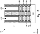
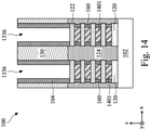
- Figs. 5-8 and 11-14 illustrate cross-sectional views along line B-B of structure of Fig. 4 at various stages of its fabrication, according to some embodiments.
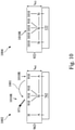
- Figs. 9 and 10 illustrate various scenarios of an etching process to form inner spacer structure 160 in method 300 , according to some embodiments. Operations can be performed in a different order or not performed depending on specific applications.
- Method 300 may not produce a complete semiconductor device 100 . Accordingly, it is understood that additional processes can be provided before, during, and/or after method 300 , and that some other processes may be briefly described herein. Further, the discussion of elements in Figs. 1 , 2 , and 4-14 with the same annotations applies to each other, unless mentioned otherwise.
- a recess structure is formed in a fin structure.
- a recess structure 536 (shown in Fig. 5 ) can be formed in fin structure 108 (shown in Fig. 4 ) with reference to Figs. 4 and 5 .
- the process of forming recess structure 536 can include (i) forming fin structures 108 (shown in Fig. 4 ) over substrate 102 ; (ii) forming STI region 138 (shown in Fig. 4 ) over the etched substrate 102 using a deposition process and an etch back process; (iii) forming sacrificial gate structures 410 (shown in Fig. 4 ) with length L 110 over fin structures 108 ; and (iv) removing fin structures 108 through sacrificial gate structures 410 to form recess structure 536 .
- the process of forming fin structures 108 can include (i) providing substrate 102 ; (ii) epitaxially growing channel regions 122 and sacrificial layers 322 over substrate 102 ; and (iii) etching channel regions 122 , sacrificial layers 322 , and substrate 102 through a patterned mask layer (not shown in Fig. 4 ) using an etching process.
- Sacrificial layer 322 can be made of materials different from channel region 122 and similar to (e.g., lattice mismatch within 5%) substrate 102 .
- sacrificial layer 322 can be made of SiGe, and channel region 122 can be made of Si.
- sacrificial layer 322 and channel region 122 can be made of SiGe with different atomic percentage of Ge from each other.
- Channel region 122 and sacrificial layer 322 can have suitable thicknesses t 422 and t 322 , respectively. In some embodiments, each of thicknesses t 422 and t 322 can be from about 5 nm to about 10 nm.
- Channel region 122 and sacrificial layer 322 can be epitaxially grown using any suitable epitaxial growth process, such as a chemical vapor deposition (CVD) process, a low pressure CVD (LPCVD) process, a rapid thermal CVD (RTCVD) process, a metal-organic CVD (MOCVD) process, an atomic layer CVD (ALCVD) process, an ultrahigh vacuum CVD (UHVCVD) process, a reduced pressure CVD (RPCVD) process, a molecular beam epitaxy (MBE) process, a cyclic deposition-etch (CDE) process, and a selective epitaxial growth (SEG) process.
- CVD chemical vapor deposition
- LPCVD low pressure CVD
- RTCVD rapid thermal CVD
- MOCVD metal-organic CVD
- ACVD atomic layer CVD
- UHVCVD ultrahigh vacuum CVD
- RPCVD reduced pressure CVD
- MBE molecular beam epitaxy
- the etching process for removing channel region 122 , sacrificial layer 322 , and substrate 102 can include a dry etching process or a wet etching process to define fin structure 108 with any suitable width W 108 , such as from about 5 nm to about 50 nm.
- the dry etching process can include using any suitable etchant, such as an oxygen-containing gas, a fluorine-containing gas, a chlorine-containing gas, and a bromine-containing gas
- the wet etching process can include etching in any suitable wet etchant, such as diluted hydrofluoric acid, potassium hydroxide solution, ammonia, and nitric acid. Based on the disclosure herein, other widths and etching processes for fin structure 108 are within the spirit and scope of this disclosure.
- the deposition process for forming STI region 138 can include any suitable growth process, such as a physical vapor deposition (PVD) process, a CVD process, a high-density-plasma (HDP) CVD process, a flowable CVD (FCVD) process, and an atomic layer deposition (ALD) process.
- the etch back process for forming STI region 138 can include a dry etching process, a wet etching process, or a polishing process, such as chemical vapor deposition (CMP) process. Based on the disclosure herein, other processes for forming STI region 138 are within the spirit and scope of this disclosure.
- the process of forming sacrificial gate structure 410 can include (i) blanket depositing a dielectric layer 406 with a suitable thickness, such as from about 1 nm to about 5 nm, over fin structures 108 using a suitable deposition process, such as a CVD process, a PVD process, and an ALD process; (ii) blanket depositing a polysilicon layer (not shown in Fig. 4 ) and a hard mask layer (not shown in Fig.
- gate spacers 104 with a suitable thickness t 104 , such as from about 5 nm to about 15 nm, over the polysilicon layer's side surfaces and/or over fin structure 108 's side surfaces using a suitable deposition process and an etching process.
- a suitable deposition process such as a CVD process, a PVD process, and an ALD process
- removing dielectric layer 406 , the polysilicon layer and the hard mask layer through a patterned mask layer (not shown in Fig. 4 ) using an etching process
- gate spacers 104 with a suitable thickness t 104 , such as from about 5 nm to about 15 nm, over the polysilicon layer's side surfaces and/or over fin structure 108 's side surfaces using a suitable deposition process and an etching process.
- recess structure 536 can be formed by removing channel regions 122 , sacrificial layers 322 , and substrate 102 through sacrificial gate structures 410 and gate spacers 104 using an etching process.
- the etching process can include a dry etching process or a wet etching process. In some embodiments, the etching process can be a time-etching process.
- the dry etching process can include using any suitable etchant, such as an oxygen-containing gas, a fluorine-containing gas, a chlorine-containing gas, and a bromine-containing gas
- the wet etching process can include etching in any suitable wet etchant, such as diluted hydrofluoric acid, potassium hydroxide solution, ammonia, and nitric acid.
- the resulting recess structure 536 can expose fin structure 108 's side surface, such as exposing sacrificial layer 322 's side surface 322S and exposing channel region 122 's side surface 122S .
- the resulting recess structure 536 can expose gate spacers 104 's side surfaces. Further, the resulting recess structure can define a suitable channel region 122 's length L 522 , such as from about 10 nm to about 50 nm. In some embodiments, length L 522 can be substantially equal to the sum of length L 110 and twice of thickness t 104 . In some embodiments, an upper channel region 122 's length L 522 (e.g., length L 522A ) can be substantially equal to a lower channel region 122 's length L 522 (e.g., length L 522B ).
- a standard deviation of the upper channel region 122 's length L 522 (e.g., length L 522A ) and the lower channel region 122 's length L 522 (e.g., length L 522B ) can be less than about 1 nm.
- a dielectric layer is formed in the recess structure.
- dielectric layer 762 (shown in Fig. 7 ) can be formed in fin structure 108 of Fig. 5 .
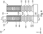
- the process of forming dielectric layer 762 can include forming recess structures 636 (shown in Fig. 6 ) in Fig 5 's sacrificial layers 322 with a suitable etching depth S 636 , such as from about 2 nm to about 10 nm, using a selective etching process that can selectively etch sacrificial layer 322 from channel region 122 .
- etching depth S 636 can be less than or substantially equal to gate spacer 104 's thickness t 104 .
- the selective etching process can form a curved side surface 322S exposed by recess structure 636 .
- the process of forming dielectric layer 762 can further include blanket depositing dielectric layer 762 in recess structure 436 and in recess structures 636 using a deposition process, such as a CVD process, a PVD process, and an ALD process.
- the deposited dielectric layer 762 can cover fin structure 108 's side surface, such as covering sacrificial layer 322 's side surface 322S and covering channel region 122 's side surface 122S .
- the deposited dielectric layer 762 can be a substantially conformal dielectric layer covering fin structure 108 's top and side surfaces.
- dielectric layer 762 can have a thickness H 762 over sacrificial gate structure 410 and a thickness t 762 over channel region 122 's side surface 122S , where thickness H 762 can be substantially equal to thickness t 762 .
- the deposited dielectric layer 762 can substantially fill recess structure 636 .
- the deposited dielectric layer 762 can have two opposite side surfaces horizontally (e.g., in the x-direction) separated from one another in recess structure 536 .
- a cyclic etching process is performed to remove the dielectric layer.
- a portion of dielectric layer 762 e.g., from Fig. 7
- the cyclic etching process can be an oxygen-free dry etching process to define inner spacer structure 160 by selectively etching dielectric layer 762 of Fig. 7 over channel region 122 .
- the cyclic etching process does not apply oxygen-contained etchants (e.g., etchants' chemical formula that does not include oxygen) to etch dielectric layer 762 .
- the cyclic etching process can include one or more cycles of a radical etching process that can laterally and selectively etch dielectric layer 762 over channel region 122 's surface 122S to define inner spacer structure 160 .
- the cyclic etching process can etch dielectric layer 762 at a first etching rate and etch channel region 122 at a second etching rate, where a ratio of the first etching rate to the second etching rate can be from about 3 to about 50, from about 5 to about 50, from about 5 to about 40, from about 5 to about 30, or from about 5 to about 20. If the ratio is below the above-noted lower limits, the cyclic etching process may damage channel region 122 , thus reducing the yield of semiconductor device 100 . If the ratio is beyond the above-noted upper limits, the cyclic etching process may consume more process gases, thus increasing a manufacturing cost of semiconductor device 100.
- the above-noted lower and upper limits are determined based on the activation discrepancies (caused at least by the choice of processing gas species; discussed below with reference to Figs. 9 and 10 ) in the cyclic etching process.
- the cyclic etching process can selectively etch dielectric layer 762 over channel region 122 , the resulting channel region 122 's thickness t 122 after the cyclic etching process can be substantially equal to thickness t 422 defined at operation 305 (shown in Fig. 5 ).
- the resulting channel layer 122 's length L 122 after the cyclic etching process can be substantially equal to length L 522 defined at operation 305 (shown in Fig. 5 ).
- an upper channel region 122 's length L 122 e.g., length L 122A
- a lower channel region 122 's length L 122 e.g., length L 122B
- a standard deviation of the upper channel region 122 's length L 122 (e.g., length L 122A ) and the lower channel region 122 's length L 122 (e.g., length L 122B ) can be less than about 1 nm.
- each cycle of the cyclic etching process can include a first dry etching process.
- the process of performing the first dry etching process can include (i) providing a first processing gas that contains a first halogen element; and (ii) generating particle beams 910R (e.g., radicals or ions) by performing an excitation process, a disassociation process, and/or an ionization process on the first processing gas.
- particle beams 910R e.g., radicals or ions
- the first processing gas can include nitrogen trifluoride (NF 3 ), fluorine gas (F 2 ), carbon tetrafluoride (CF 4 ),or fluoroform (CHF 3 ), where the respective first halogen element of the first processing gas can be a fluorine element (F) and the respective particle beams 910R can contain fluorine-based radicals and/or fluorine-based plasmas.
- particle beams 910R can be substantially made of radicals (e.g., does not contain ions).
- Particle beams 910R can adsorb on dielectric layer 762 to form an interfacial layer 962 over dielectric layer 762 .
- particle beams 910R can adsorb on dielectric layer 762 's silicon sites to form bonding Si- 910 (e.g., Si-F bonding) in interfacial layer 962 , where element 910 can represent the first halogen element (e.g., fluorine element, F) of the first processing gas.
- Si- 910 e.g., Si-F bonding
- element 910 can represent the first halogen element (e.g., fluorine element, F) of the first processing gas.
- Particle beams 910R can further adsorb on dielectric layer 762 's element A's sites to form bonding A-910 (e.g., N-F bonding) in interfacial layer 962 .
- element A in dielectric 762 can include a nitrogen element, a carbon element, or an oxygen element.
- dielectric layer 762 can be a low-k dielectric material (e.g., SiCN) that contains a nitrogen element and particle beams 910R can be fluorine-based radicals, where the respective bonding Si- 910 can be a Si-F bonding and the respective bonding A-910 can be a N-F bonding.
- particle beams 910R can be fluorine-based radicals, where the respective volatile byproduct 971 can be silicon fluoride (SiF 4 ).
- the process of performing the first dry etching process of each cycle of the cyclic etching process can further include (i) providing another processing gas that contains element hydrogen (H); and (ii) generating particle beams 912R (e.g., hydrogen-contained radicals or hydrogen-contained plasmas) by performing an excitation process, a dislocation process, and/or an ionization process on the other processing gas.
- the other processing gas that contains element hydrogen can include hydrogen gas (H2), phosphine (PH 3 ), ammonia (NH 3 ), or methane (CH4). As shown in Fig.
- particle beams 912R can interact with A-910 bonding (e.g., N-F bonding) to migrate (e.g., represented by arrow 901 ) element 910 (e.g., F element) from element A sites (e.g., nitrogen sites) to adjacent silicon sites (e.g., the adjacent Si- 910 bonding).
- element 910 e.g., F element
- the migrated elements 910 can therefore react with bonding Si- 910 (e.g., Si-F bonding) to form volatile byproduct 971 , thus enhancing the first dry etching process's etching rate of etching dielectric layer 762 .
- Si- 910 e.g., Si-F bonding
- particle beams 912R can adsorb on dielectric layer 762 's element A 's sites to form bonding A-H (e.g., N-H bonding) in interfacial layer 962 .
- A-H e.g., N-H bonding
- the reaction rate and/or the adsorption rate of particle beams 910R with dielectric layer 762 's silicon site can be increased to form volatile byproduct 971 , thus enhancing the first dry etching process's etching rate of etch dielectric layer 762 .
- the first dry etching process of each cycle of the cyclic etching process may slightly etch channel region 122 .
- particle beams 910R may adsorb on channel region 122 's silicon sites by forming bonding Si- 910 (e.g., Si-F bonding) in interfacial layer 922 over channel region 122 .
- the subsequent incoming particle beams 910R e.g., F radicals
- bonding Si- 910 e.g., Si-F bonding
- particle beams 912R may adsorb on channel region 122' s silicon sites by forming bonding Si-H bonding in interfacial layer 922 over channel region 122 .
- the subsequent generated particle beams 912R may further react with Si-H bonding to form volatile SiH 4 to etch channel region 122 .
- particle beams 912R can boost the adsorption rate of the element 910 (e.g., the first fluorine element, such as F, from the first processing gas) on dielectric layers 762 's silicon site. Accordingly, the first dry etching process can etch dielectric layer 762 at a greater etching rate than etching channel region 122 .
- the element 910 e.g., the first fluorine element, such as F
- an activation energy discrepancy between scenarios 902/904 and scenarios 906/908 can be less than about 0.1 eV, such that the first dry etching process can etch dielectric layer 762 at an etching rate greater than or substantially equal to an etching rate of etching channel region 122 .
- a ratio of an etching rate of etching dielectric layer 762 via the first dry etching process to an etching rate of etching channel region 122 via the first dry etching process can be from about 0.5 to about 5 or from about 1 to about 3. If the ratio is below the above-noted lower limits, the first dry etching process may cause extra damages on channel region 122 , thus reducing the yield of semiconductor device 100 .
- the first dry etching process may consume more process gases, thus increasing a manufacturing cost of semiconductor device 100.
- the above-noted upper and lower limits are determined by the above-noted activation energy's discrepancy between scenarios 902/904 and scenarios 906/908 .
- each cycle of the cyclic etching process can further include a second dry etching process subsequently followed by the first dry etching process.
- the process of performing the second dry etching process can include (i) providing a second processing gas that contains a second halogen element; and (ii) generating particle beams 1010R (e.g., radicals or plasmas) by performing an excitation process, a disassociation process, and/or an ionization process on the second processing gas.
- particle beams 1010R can be substantially made of radicals (e.g., does not contain ions).
- the second halogen element associated with the second dry etching process can be different from the first halogen element associated with the first dry etching process.
- the second halogen element's atomic mass can be greater than the first halogen element's atomic mass.
- the second halogen element associated with the second dry etching process can be a chlorine element (CI)
- the first halogen element associated with the first dry etching process can be a fluorine element (F).
- the second processing gas that contains the second halogen element can be free from containing the first halogen element (e.g., the second processing gas does not contain the first halogen element).
- the first halogen element associated with the first dry etching process can be a fluorine element (F), where the second processing gas can be fluorine-free (e.g., the second processing gas's chemical formula does not contain fluorine element).
- the second processing gas can include chlorine gas (Cl 2 ), silicon tetrachloride (SiCl 4 ), or boron trichloride (BCl 3 ), where the second halogen element of the second processing gas can be a chlorine element (CI) and the respective particle beams 1010R can contain chlorine-based radicals and/or chlorine-based plasmas.
- CI chlorine element
- particle beams 1010R e.g., Cl radicals
- dielectric layer 762 's bonding A-910 e.g., N-F bonding
- element 91 0 F elements; the first halogen element from element A sites (e.g., nitrogen sites) to adjacent silicon sites (e.g., the adjacent Si-F bonding).
- the migrated elements 910 can therefore react with bonding Si- 910 (Si-F bonding) to form volatile byproduct 971 (e.g., SiF 4 ), thus causing the etching of dielectric layer 762 during the second dry etching process.
- particle beams 1010R e.g., Cl radicals
- Si-Cl bonding Si-Cl bonding; not shown in Fig. 10 's scenario 1002
- A-1010 bonding N-Cl bonding; not shown in Fig.
- the subsequent generated particle beams 1010R during the second etching process can further react with bonding Si- 1010 and bonding A-1010 with a sufficient low activation energy (e.g., less than about 0.5 eV or less than about 0.1 eV) to cause the etching of dielectric layer 762 .
- a sufficient low activation energy e.g., less than about 0.5 eV or less than about 0.1 eV
- the second dry etching process can have a negligible etching rate of etching channel region 122 .
- particle beams 1010R may adsorb on channel region 122 's silicon sites or react with Si- 910 (e.g., Si-F bonding formed by the first dry etching process).
- Si- 910 e.g., Si-F bonding formed by the first dry etching process.
- the adsorption of particle beams 1010R on channel region 122 can form bonding Si- 1010 (e.g., Si-Cl bonding) in interfacial layer 922 over channel region 122 .
- the subsequent generated particle beams 1010R may further react with bonding Si- 1010 with an activation energy greater than scenario 1002 's activation energy.
- scenario 1004 's activation energy can be greater than scenario 1002 's activation energy by at least about 0.1 eV, such as from about 0.1 eV to about 0.5 eV.
- the second dry etching process can selectively etch dielectric layer 762 (shown in scenario 1002 ) over channel region 122 (shown in scenario 1004 ).
- a ratio of an etching rate of etching dielectric layer 762 via the second dry etching process to an etching rate of etching channel region 122 via the second dry etching process can be from about 5 to about 50, from about 5 to about 40, from about 5 to about 30, or from about 5 to about 20.
- the second dry etching process may cause extra damages on channel region 122 , thus reducing the yield of semiconductor device 100 . If the ratio is beyond the above-noted upper limits, the second dry etching process may consume more process gases, thus increasing a manufacturing cost of semiconductor device 100 .
- the above-noted upper and lower limits are determined by the above-noted activation energy's discrepancy between scenarios 1002 and 1004 .
- the second dry etching process can provide a greater etching selectivity to etch dielectric layer 762 over channel region 122 than to the first dry etching process. Since the activation energy difference (e.g., less than about 0.1 eV) between scenarios 902/904 and scenarios 906/908 can be less than that (e.g., greater than about 0.1 eV) between scenario 1002 and scenario 1004 , the second dry etching process can provide a greater etching selectivity to etch dielectric layer 762 over channel region 122 than to the first dry etching process.
- the activation energy difference e.g., less than about 0.1 eV
- scenarios 902/904 and scenarios 906/908 can be less than that (e.g., greater than about 0.1 eV) between scenario 1002 and scenario 1004
- the second dry etching process can provide a greater etching selectivity to etch dielectric layer 762 over channel region 122 than to the first dry etching process.
- a ratio of the second dry etching process's etching selectivity (e.g., a ratio of an etching rate of etching dielectric layer 762 using the second dry etching process to an etching rate of etching channel region 122 using the second dry etching process) to the first dry etching process's etching selectivity (e.g., a ratio of an etching rate of etching dielectric layer 762 using the first dry etching process to an etching rate of etching channel region 122 using the first dry etching process) can be from about 1 to about 20, from about 2 to about 20, from about 2 to about 15, from about 2 to about 10, or from about 2 to about 5.
- the first dry etching process may cause extra damages on channel region 122 , thus reducing the yield of semiconductor device 100 .
- the second dry etching process may consume more process gases, thus increasing a manufacturing cost of semiconductor device 100 .
- the above-noted upper and lower limits are determined by (i) the activation energy's discrepancy between scenarios 902/904 and scenarios 906/908 and (ii) the activation energy's discrepancy between scenario 1002 and scenario 1004 .
- the second dry etching process can provide a lower etching rate to etch channel region 122 than the first dry etching process.
- a ratio of an etching rate of etching channel region 122 via the second dry etching process to an etching rate of etching channel region 122 via the first dry etching process can be from about 0.05 to about 1, from about 0.05 to about 0.8, from about 0.05 to about 0.6, from about 0.05 to about 0.4, from about 0.05 to about 0.2, or from about 0.05 to about 0.1.
- the first dry etching process may cause extra damages on channel region 122 , thus reducing the yield of semiconductor device 100 .
- the second dry etching process may cause extra damages on channel region 122 , thus reducing the yield of semiconductor device 100 .
- the above-noted upper and lower limits are determined by (i) the activation energy's discrepancy between scenarios 902/904 and scenarios 906/908 and (ii) the activation energy's discrepancy between scenario 1002 and scenario 1004 .
- the first and second dry etching processes can etch dielectric layer 762 with substantially equal etching rates to one another.
- the second dry etching process's etching selectivity can be greater than the first dry etching process's etching selectivity, it is desirable to provide less radio frequency (RF) power for the first dry etching process than for the second dry etching process to increase an overall etching selectivity of the cyclic etching process to etch dielectric layer 762 over channel region 122 .
- RF radio frequency
- the process of generating particle beams 910R and 1010R for the first and second dry etching processes can include providing first and second RF powers, respectively, where a ratio of the first RF power to the second RF power can be from about 0.05 to about 1, from about 0.05 to about 0.8, from about 0.05 to about 0.6, from about 0.05 to about 0.4, or from about 0.05 to about 0.2. If the ratio of the first RF power to the second RF power is above these upper limits, the overall cyclic etching process may provide an insufficient etching selectivity to etch dielectric layer 762 from channel region 122 , because the first dry etching process may have an inferior etching selectivity to the second dry etching process as previously discussed. If the ratio of the first RF power to the second RF power is below the above-noted lower limit, the first dry etching process may not have sufficient energy to form particle beams 910R and/or 912R.
- the second dry etching process's etching selectivity can be greater than the first dry etching process's etching selectivity, it is desirable to perform a lower etching time duration for the first dry etching process than for the second dry etching process to increase an overall etching selectivity of the cyclic etching process to etch dielectric layer 762 over channel region 122.
- the first and second dry etching processes can be performed for a first and second etching time durations, respectively, where a ratio of the first etching time duration to the second etching time duration can be from about 0.05 to about 1, from about 0.05 to about 0.8, from about 0.05 to about 0.6, from about 0.05 to about 0.4, or from about 0.05 to about 0.2. If the ratio of the first time duration to the second time duration is above these upper limits, the overall cyclic etching process may provide an insufficient etching selectivity to etch dielectric layer 762 from channel region 122 , because the first dry etching process may have an inferior etching selectivity to the second dry etching process as previously discussed. If the ratio of the first time duration to the second time duration is below the above-noted lower limit, the first dry etching process may not have sufficient time duration to form particle beams 910R and/or 912R.
- the second dry etching process's etching selectivity can be greater than the first dry etching process's etching selectivity, it is desirable to provide the first processing gas with a reduced flow rate for the first dry etching process and provide the second processing gas with an increased flow rate for the second dry etching process to increase an overall etching selectivity of the cyclic etching process to etch dielectric layer 762 over channel region 122 .
- the processes of performing the first and second dry etching processes can include providing the first and second processing gases with a first and second flow rates, respectively, where a ratio of the first flow rate to the second flow rate can be from about 0.05 to about 1, from about 0.05 to about 0.8, from about 0.05 to about 0.6, from about 0.05 to about 0.4, or from about 0.05 to about 0.2. If the ratio of the first flow rate to the second flow rate is above these upper limits, the overall cyclic etching process may provide an insufficient etching selectivity to etch dielectric layer 762 from channel region 122 , because the first dry etching process may have an inferior etching selectivity to the second dry etching process as previously discussed. If the ratio of the first flow rate to the second flow rate is below the above-noted lower limit, the first dry etching process may not have sufficient processing gas to form particle beams 910R and/or 912R.
- the second dry etching process's etching selectivity can be greater than the first dry etching process's etching selectivity, it is desirable to provide the first processing gas with a reduced dispensing time duration for the first dry etching process and provide the second processing gas with an increased dispensing time duration for the second dry etching process to increase an overall etching selectivity of the cyclic etching process to etch dielectric layer 762 over channel region 122 .
- the processes of performing the first and second dry etching processes can include providing the first and second processing gases with a first and second dispensing time durations, respectively, where a ratio of the first dispensing time duration to the second dispensing time duration can be from about 0.05 to about 1, from about 0.05 to about 0.8, from about 0.05 to about 0.6, from about 0.05 to about 0.4, or from about 0.05 to about 0.2.
- the overall cyclic etching process may provide an insufficient etching selectivity to etch dielectric layer 762 from channel region 122 , because the first dry etching process may have an inferior etching selectivity to the second dry etching process as previously discussed. If the ratio of the first dispensing time duration to the second dispensing time duration is below the above-noted lower limit, the first dry etching process may not have sufficient processing gas to form particle beams 910R and/or 912R.
- the first processing gas that contains the first halogen element can be free from containing the second halogen element (e.g., the first processing gas does not contain the second halogen element).
- the second halogen element associated with the second dry etching process can be a chlorine element (CI), where the first processing gas can be chlorine-free (e.g., the first processing gas's chemical formula does not contain chlorine).
- the cyclic etching process can perform the next cycle's first dry etching process to etch dielectric layer 762 and form bonding A-910 at interfacial layer 962 as previously discussed in Fig. 9 , and subsequently perform the next cycle's second dry etching process to migrate the element A to selectively etch dielectric layer 762 over channel region 122 as previously discussed in Fig. 10 .
- the cyclic etching process for defining inner spacer structure 160 can be an atomic layer etching process ("ALE mode").
- the first dry etching process can form interfacial layers 962 and 922 as self-limited surface layers that (i) do not react with incoming particle beams 910R and 912R , and (ii) prevents the underlying dielectric layer 762 and channel region 122 from reacting with incoming particle beams 910R and 912R .
- the second dry etching process can selectively etch interfacial layer 962 over the underlying dielectric layer 762 and/or channel region 122 .
- interfacial layer 962 in the ALE mode, since interfacial layer 962 can be a self-limited surface layer, interfacial layer 962 can have a substantially constant thickness t 962 , such as from about 0.1 nm to about 1.0 nm and from about 0.1 nm to about 0.5 nm, regardless the time duration of the first etching process.
- interfacial layer 922 in the ALE mode, since interfacial layer 922 can be a self-limited surface layer, interfacial layer 922 can have a substantially constant thicknesses t 922 , such as from about 0.1 nm to about 1.0 nm and from about 0.1 nm to about 0.5 nm, regardless of the time duration of the first etching process.
- each cycle of the cyclic etching process in the ALE mode, each cycle of the cyclic etching process can etch a substantially equal thickness (e.g., substantially equal to thickness t 962 ) of dielectric layer 7
- a source/drain (S/D) region is formed in the recess structure.
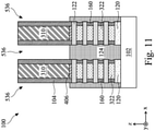
- S/D region 124 can be formed in recess structures 536 and over inner spacer structures 160 .
- the process of forming S/D region 124 can include epitaxially growing S/D region 124 in the structure of Fig. 8 using an epitaxial growth process, such as a CVD process, a LPCVD process, a RTCVD process, a MOCVD process, an ALCVD process, a UHVCVD process, a RPCVD process, an MBE process, a CDE process, and an SEG process.
- the epitaxial growth process can be performed using suitable precursors, such as silane (SiH4), disilane (Si 2 H 6 ), dichlorosilane (DCS), and germane (GeH 4 ).
- the epitaxial growth process can further include doping S/D region 124 using suitable dopant precursors, such as diborane (B 2 H 6 ), boron trifluoride (BF 3 ), phosphine (PH 3 ), and arsine (AsH 3 ). Accordingly, the resulting S/D region 124 can be grown over and in contact with channel regions 122 under sacrificial gate structure 410 and gate spacers 104 .
- the resulting S/D region 124 can be further grown over and in contact with inner spacer structures 160 that are vertically (e.g., in the z-direction) sandwiched by two vertical (e.g., in the z-direction) channel regions 122 .
- inner spacer structures 160 that are vertically (e.g., in the z-direction) sandwiched by two vertical (e.g., in the z-direction) channel regions 122 .
- other epitaxial growth processes for forming S/D region 124 are within the spirit and scope of this disclosure.
- a metal gate structure is formed over the fin structure.
- gate structure 110 (shown in Fig. 2 ) can be formed over fin structure 108 .
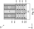
- the process of forming gate structure 110 can include (i) forming ILD layer 130 (shown in Fig. 12 ) coplanarized with sacrificial gate structures 410 of Fig. 11 using a suitable deposition process, such as a PVD process and a CVD process, and a suitable etch back process, such as a chemical mechanical polishing (CMP) process; (ii) removing sacrificial layer 348 to form recess structures 1336 (shown in Fig.
- CMP chemical mechanical polishing
- the etching process for forming recess structure 1336 can include a dry etching process that uses chlorine, fluorine or bromine as gas etchants.
- the etching process for forming recess structure 1336 can include a wet etching process that uses an ammonium hydroxide (NH 4 OH), sodium hydroxide (NaOH), or potassium hydroxide (KOH) as wet etchants.
- the etching process for removing dielectric layer 306 can include a dry etching process that uses chlorine, fluorine or bromine as gas etchants. In some embodiments, the etching process for removing dielectric layer 306 can include a wet etching process that uses an hydrogen fluoride (HF) as wet etchants.
- HF hydrogen fluoride
- the process of forming gate structure 110 can further include (i) removing sacrificial layers 322 of Fig. 13 to form recess structures 1401 (shown in Fig. 14 ) and using a plasma etching process or a radical etching process; and filling a gate dielectric layer (not shown in Fig. 2 ) and a gate electrode (not shown in Fig. 2 ) in the recess structures 1401 of Fig. 14 using a suitable deposition process, such as an ALD process and a CVD process, and a suitable etch back process, such as a CMP process.
- a suitable deposition process such as an ALD process and a CVD process
- a suitable etch back process such as a CMP process.
- the present disclosure provides an exemplary transistor inner spacer structure and a method for forming the same.
- the method of forming the inner spacer structure can include depositing a dielectric layer over a fin structure's side surface and performing a cyclic dry etching process to selectively etch the dielectric layer over the fin structure.
- the cyclic dry etching process can be an oxygen-free radical etching process.
- each cycle of the cyclic etching process can include a first radical etching process and a second radical etching process.
- the first radical etching process can apply a first halogen radical, such as a F radical, to etch the dielectric layer.
- the first radical etching process may adsorb the first halogen radical on the dielectric surface to form an interfacial layer.
- the second radical etching process can apply a second halogen radical, such as a Cl radical, to react with the interfacial layer to further etch the dielectric layer.
- the first and/or the second radical etching processes can selectively etch the dielectric layer over the fin structure. Further, the first and the second radical etching processes can be performed without breaking the vacuum in between.
- a benefit of the present disclosure, among others, is to provide an oxygen-free dry etching method to form the inner spacer structure with an improved thickness uniformity and a higher etching rate, thus improving the semiconductor device's reliability and throughput.
- a method can include forming a fin structure over a substrate.
- the fin structure can include a first channel layer and a sacrificial layer.
- the method can further include forming a first recess structure in a first portion of the fin structure, forming a second recess structure in the sacrificial layer of a second portion of the fin structure, forming a dielectric layer in the first and second recess structures, and performing an oxygen-free cyclic etching process to etch the dielectric layer to expose the channel layer of the second portion of the fin structure.
- the process of performing the oxygen-free cyclic etching process can include performing a first etching process to selectively etch the dielectric layer over the channel layer of the second portion of the fin structure with a first etching selectivity, and performing a second etching process to selectively etch the dielectric layer over the channel layer of the second portion of fin structure with a second etching selectivity greater than the first etching selectivity.
- a method can include forming a fin structure over a substrate, forming a recess structure in the fin structure, forming a dielectric layer over the recess structure, and performing an oxygen-free cyclic etching process to etch the dielectric layer.
- the process of performing the oxygen-free cyclic etching process can include performing a first etching process with a first etchant to remove a first portion of the dielectric layer and performing a second etching process with a second etchant to remove a second portion of the dielectric layer.
- the first etchant can include a first halogen element.
- the second etchant can include a second halogen element different from the first halogen element.
- a method can include forming a gate structure over a first portion of a substrate, forming a recess structure over a second portion of the substrate, forming a dielectric layer in the recess structure and over the second portion of the substrate, performing a cyclic etching process to etch the dielectric layer to expose the second portion of the substrate, and forming a source/drain (S/D) contact structure in the recess structure and over the dielectric layer.
- the process of performing the cyclic etching process can include performing a first etching process to remove a first portion of the dielectric layer, and performing a second etching process to remove a second portion of the dielectric layer.
- the process of performing the first etching process can include etching the first portion of the substrate at a first etching rate.
- the process of performing the second etching process can include etching the first portion of the substrate with a second etching rate less than the first etching rate.
Landscapes
- Insulated Gate Type Field-Effect Transistor (AREA)
- Physics & Mathematics (AREA)
- Engineering & Computer Science (AREA)
- Plasma & Fusion (AREA)
- Thin Film Transistor (AREA)
- Drying Of Semiconductors (AREA)
Abstract
The present disclosure describes a semiconductor structure and a method for forming the same. The method can include forming a fin structure over a substrate. The fin structure can include a first channel layer and a sacrificial layer. The method can further include forming a first recess structure in a first portion of the fin structure, forming a second recess structure in the sacrificial layer of a second portion of the fin structure, forming a dielectric layer in the first and second recess structures, and performing an oxygen-free cyclic etching process to etch the dielectric layer to expose the channel layer of the second portion of the fin structure. The process of performing the oxygen-free cyclic etching process can include performing a first etching process to selectively etch the dielectric layer over the channel layer of the second portion of the fin structure with a first etching selectivity, and performing a second etching process to selectively etch the dielectric layer over the channel layer of the second portion of fin structure with a second etching selectivity greater than the first etching selectivity
Description
- Advances in semiconductor technology has increased the demand for semiconductor devices with higher storage capacity, faster processing systems, higher performance, and lower costs. To meet these demands, the semiconductor industry continues to scale down the dimensions of semiconductor devices, such as nano-sheet FETs. Such scaling down has increased the complexity of semiconductor manufacturing processes.
- Aspects of this disclosure are best understood from the following detailed description when read with the accompanying figures.
-
Fig. 1 is an isometric view of a semiconductor device, according to some embodiments. -
Fig. 2 is a cross-sectional view of a semiconductor device, according to some embodiments. -
Fig. 3 is a flow diagram of a method for fabricating a semiconductor device, according to some embodiments. -
Fig. 4 is an isometric view of a semiconductor device at a stage of its fabrication process, according to some embodiments. -
Figs. 5-8 are cross-sectional views of a semiconductor device at various stages of its fabrication process, according to some embodiments. -
Fig. 9 and10 illustrate various scenarios of an etching process for fabrication of a semiconductor device, according to some embodiments. -
Figs. 11-14 are cross-sectional views of a semiconductor device at various stages of its fabrication process, according to some embodiments. - Illustrative embodiments will now be described with reference to the accompanying drawings. In the drawings, like reference numerals generally indicate identical, functionally similar, and/or structurally similar elements.
- It is noted that references in the specification to "one embodiment," "an embodiment," "an example embodiment," "exemplary," etc., indicate that the embodiment described may include a particular feature, structure, or characteristic, but every embodiment may not necessarily include the particular feature, structure, or characteristic. Moreover, such phrases do not necessarily refer to the same embodiment. Further, when a particular feature, structure or characteristic is described in connection with an embodiment, it would be within the knowledge of one skilled in the art to effect such feature, structure or characteristic in connection with other embodiments whether or not explicitly described.
- It is to be understood that the phraseology or terminology herein is for the purpose of description and not of limitation, such that the terminology or phraseology of the present specification is to be interpreted by those skilled in relevant art(s) in light of the teachings herein.
- Spatially relative terms, such as "beneath," "below," "lower," "above," "upper," and the like may be used herein for ease of description to describe one element or feature's relationship to another element(s) or feature(s) as illustrated in the figures. The spatially relative terms are intended to encompass different orientations of the device in use or operation in addition to the orientation depicted in the figures. The apparatus may be otherwise oriented (rotated 90 degrees or at other orientations) and the spatially relative descriptors used herein may likewise be interpreted accordingly.
- In some embodiments, the terms "about" and "substantially" can indicate a value of a given quantity that varies within 5 % of the value (e.g., ±1 %, ±2 %, ±3 %, ±4 %, ±5 % of the value). These values are merely examples and are not intended to be limiting. The terms "about" and "substantially" can refer to a percentage of the values as interpreted by those skilled in relevant art(s) in light of the teachings herein.
- As used herein, the term "vertical" means nominally perpendicular to the surface of a substrate.
- Fins associated with fin field effect transistors (finFETs) or gate-all-around (GAA) FETs can be patterned by any suitable method. For example, the fins can be patterned using one or more photolithography processes, including a double-patterning process or a multi-patteming process. Double-patterning and multi-patterning processes can combine photolithography and self-aligned processes, allowing patterns to be created that have, for example, pitches smaller than what is otherwise obtainable using a single, direct photolithography process. For example, a sacrificial layer is formed over a substrate and patterned using a photolithography process. Spacers are formed alongside the patterned sacrificial layer using a self-aligned process. The sacrificial layer is then removed, and the remaining spacers can then be used to pattern the fins.
- Technology advances in the semiconductor industry drive the pursuit of integrated circuits (ICs) having higher device density, higher performance, and lower cost. In the course of the IC evolution, nano-sheet transistors can replace planar field effect transistor (FET) and fin field-effect transistor (finFET) to achieve ICs with higher device densities. Nano-sheet transistors can use a gate-all-around (GAA) gate structure to surround each nano-sheet channel layer to effectively reconcile short channel effects. Nano-sheet transistors require an inner spacer to physically separate the nano-sheet transistor's source-drain (S/D) regions from the nano-sheet transistor's GAA gate structure. The process of forming the inner spacer can include an inner spacer trimming process that removes an inner spacer material between the S/D region and the nano-sheet channel layer. The inner spacer trimming process may not be a wet etching process, because the wet etching process may not provide a sufficient wafer-scale etching uniformity for achieving the inner spacer with wafer-scale thickness uniformity. The inner spacer trimming process can be a dry etching process with an inner-spacer-dry-etchant to etch the inner spacer material. To protect the nano-sheet channel layer from being damaged by the dry etching process, the dry etching process can further include an oxygen radical to reduce an adsorption of the inner-spacer-dry-etchant on the nano-sheet channel layer. However, the oxygen-contained etchant can also reduce the adsorption of the inner-spacer-dry-etchant on the inner spacer material. The reduction of the adsorption of the inner-spacer-dry-etchant on the inner spacer material can degrade the inner spacer trimming process's etching rate and the inner spacer trimming process's etching uniformity, thus degrading the IC manufacturing's yield and throughput.
- To address the aforementioned challenges, the present disclosure is directed to a fabrication method of an inner spacer for a gate-all-around field effect transistor (GAA FET). The process of forming the inner spacer can include forming a recess structure in a substrate and forming a dielectric layer in the recess structure. The process of forming the inner spacer can further include performing an inner spacer dry etching process to remove the dielectric layer to expose the recess structure's side surface. The inner spacer dry etching process can be oxygen-free dry etching process (e.g., the dry etching processes do not apply any oxygen-contained etchants) to avoid the aforementioned challenges of inner spacer trimming process susceptible to the reduced etching rate and reduced etching uniformity. Further, the inner spacer dry etching process can be a cyclic dry etching process. Each cycle of the cyclic dry etching process can include a first radical etching process to etch the dielectric layer with a first etchant that includes a first halogen element. For example, the first etchant can be a fluorine radical that can adsorb onto and react with the dielectric material to etch the dielectric material. The first radical etching process can further include a hydrogen-contained etchant, such as a hydrogen radical, to increase the etching rate of etching the dielectric layer.
- The cyclic dry etching process can include a second radical etching process to etch the dielectric layer with a second etchant that includes a second halogen element. For example, the second etchant can be a chlorine radical that can facilitate the reaction between the dielectric layer and portions of the first etchants previously adsorbed on the dielectric layer's surface to etch the dielectric material. Therefore, the second radical etching process can etch the dielectric layer with a compatible (e.g., substantially equal) etching rate as the first radical etching process. The second etchant can further adsorb on the recess structure's side surface to form an interfacial layer thereon. The interfacial layer can protect the recess structure's side surface from being etched by the second radical etching process. Further, the interfacial layer can protect the recess structure's side surface from being etched by the first radical etching processes of subsequent cycles of the cyclic dry etching process. Therefore, the overall inner spacer dry etching process can have an enhanced etching rate of etching the dielectric material and an reduced etching rate of etching the recess structure's side surface. A benefit of the present disclosure, among others, is to increase the etching rate and etching selectivity of the inner spacer trimming process (e.g., the inner spacer dry etching process), thus improving the IC manufacturing's yield and throughput.
- A
semiconductor device 100 havingmultiple FETs 101 formed over asubstrate 102 is described with reference toFigs. 1 and2 , according to some embodiments.Fig. 1 illustrates an isometric view ofsemiconductor device 100, according to some embodiments.Fig. 2 illustrates a cross-sectional (e.g., along the x-z plane) view ofsemiconductor device 100 along line B-B ofFig. 1 , according to some embodiments. The discussion of elements inFigs. 1 and2 with the same annotations applies to each other, unless mentioned otherwise.Semiconductor device 100 can be included in a microprocessor, memory cell, or other integrated circuit (IC). Also, each FET 101 shown inFigs. 1 and2 can be a GAA FET, according to some embodiments. - Referring to
Fig. 1 ,substrate 102 can be a semiconductor material, such as silicon. In some embodiments,substrate 102 can include a crystalline silicon substrate (e.g., wafer). In some embodiments,substrate 102 can include (i) an elementary semiconductor, such as silicon (Si) or germanium (Ge); (ii) a compound semiconductor including silicon carbide (SiC), gallium arsenide (GaAs), gallium phosphide (GaP), indium phosphide (InP), indium arsenide (InAs), and/or indium antimonide (InSb); (iii) an alloy semiconductor including silicon germanium carbide (SiGeC), silicon germanium (SiGe), gallium arsenic phosphide (GaAsP), gallium indium phosphide (InGaP), gallium indium arsenide (InGaAs), gallium indium arsenic phosphide (InGaAsP), aluminum indium arsenide (InAlAs), and/or aluminum gallium arsenide (AlGaAs); or (iv) a combination thereof. Further,substrate 102 can be doped depending on design requirements (e.g., p-type substrate or n-type substrate). In some embodiments,substrate 102 can be doped with p-type dopants (e.g., boron (B), indium (In), aluminum (Al), or gallium (Ga)) or n-type dopants (e.g., phosphorus (P) or arsenic (As)). -
FET 101 can include afin structure 108 extending along an x-direction, agate structure 110 traversing throughfin structure 108 along a y-direction, and S/D regions 124 formed over portions offin structure 108. AlthoughFig. 1 showsfin structure 108 accommodating two FETs 101, any number ofFETs 101 can be disposed alongfin structure 108. In some embodiments,FET 101 can includemultiple fin structures 108 extending along a first horizontal direction (e.g., in the x-direction) andgate structure 110 traversing through themultiple fin structures 108 along a second horizontal direction (e.g., in the y-direction). -
Fin structure 108 can include abuffer region 120 formed oversubstrate 102.Fin structure 108 can further include one ormore channel regions 122 formed overbuffer region 120. Eachchannel region 122 can be wrapped bygate structure 110 to function asFET 101's channel. For example, a top surface, side surfaces, and a bottom surface of eachchannel region 122 can be surrounded and in physical contact withgate structure 110.Buffer region 120 andchannel region 122 can be made of materials similar to (e.g., lattice mismatch within 5%)substrate 102. In some embodiments, each ofbuffer region 120 andchannel region 122 can be made of Si or SiGe. Each ofbuffer region 120 andchannel region 122 can be un-doped, doped with p-type dopants, doped with n-type dopants, or doped with intrinsic dopants. In some embodiments,buffer region 120 andchannel regions 122 can be both doped with p-type dopants or doped with n-type dopants. -
Gate structure 110 can be a multilayered structure (not shown inFigs. 1A and 1B ) that wraps around eachchannel region 122 to modulateFET 101.Gate structure 110 can have a length L110 representing FET 101's channel length. In some embodiments, length L110 can be less than about 50 nm, less than about 40 nm, less than about 30 nm, less than about 20 nm, or less than about 15 nm. If length L110 is above these upper limits,semiconductor device 100 may not meet the fin pitch requirement determined by the respective technology node (e.g., fin pitch may be required to be less than about 60 nm for a 22 nm technology node).Gate structure 110 can include a gate dielectric layer (not shown inFigs. 1A and 1B ) and a gate electrode (not shown inFigs. 1A and 1B ) disposed on the gate dielectric layer. The gate dielectric layer can include any suitable dielectric material with any suitable thickness that can provide channel modulation forFET 101. In some embodiments, the gate dielectric layer can be made of silicon oxide or a high-k dielectric material (e.g., hafnium oxide or aluminum oxide). In some embodiments, the gate dielectric layer can have a thickness ranging from about 1 nm to about 5 nm. Based on the disclosure herein, other materials and thicknesses for the gate dielectric layer are within the spirit and scope of this disclosure. The gate electrode can function as a gate terminal forFET 101. The gate electrode can include any suitable conductive material that provides a suitable work function to modulateFET 101. In some embodiments, the gate electrode can be made of titanium nitride, tantalum nitride, tungsten nitride, titanium, aluminum, copper, tungsten, tantalum, copper, or nickel. Based on the disclosure herein, other materials for the gate electrode are within the spirit and scope of this disclosure. - S/
D regions 124 can be formed over opposite sides (e.g., along x-direction) of eachchannel region 122 andgate structure 110. S/D regions 124 can be in contact withchannel region 122'sside surface 122S to function asFET 101's source and drain terminals. S/D regions 124 can have any suitable lateral (e.g., in the y-direction) width W124 such as from about 20 nm to about 200 nm. S/D regions 124 can be made of an epitaxiallygrown semiconductor material similar to (e.g., lattice mismatch within 5%)channel region 122. In some embodiments, S/D regions 124 can be made of Si, Ge, SiGe, InGaAs, or GaAs. S/D regions 124 can be doped with p-type dopants, n-type dopants, or intrinsic dopants. In some embodiments, S/D region 124 can have a different doping type fromchannel region 122. -
Semiconductor device 100 can further include agate spacer 104 formed betweengate structure 110 and S/D region 124. In some embodiments,gate spacer 104 can be further formed overfin structure 108's side surface.Gate spacer 104 can be made of any suitable dielectric material. In some embodiments,gate spacer 104 can be made of silicon oxide, silicon nitride, or a low-k material with a dielectric constant less than about 3.9. In some embodiments,gate spacer 104 can have a suitable thickness t104 from about 5 nm to about 15 nm or from about 5 nm to about 10 nm. If thickness t104 is above these upper limits,FET 101's speed may be degraded due to a high channel resistance. If thickness t104 is below these lower limits,FET 101's speed may be degraded due to a high gate-to-source/drain parasitic capacitance. Based on the disclosure herein, other materials and thicknesses forgate spacer 104 are within the spirit and scope of this disclosure. -
Semiconductor device 100 can further include shallow trench isolation (STI)regions 138 to provide electrical isolation betweenfin structures 108. Also,STI regions 138 can provide electrical isolation betweenFET 101 and neighboring active and passive elements (not shown inFig. 1A ) integrated with or deposited onsubstrate 102.STI regions 138 can include one or more layers of dielectric material, such as a nitride layer, an oxide layer disposed on the nitride layer, and an insulating layer disposed on the nitride layer. In some embodiments, the insulating layer can include silicon oxide, silicon nitride, silicon oxynitride, fluorine-doped silicate glass (FSG), a low-k dielectric material, and/or other suitable insulating materials. Based on the disclosure herein, other dielectric materials forSTI region 138 are within the spirit and scope of this disclosure. -
Semiconductor device 100 can further include an interlayer dielectric (ILD)layer 130 to provide electrical isolation to structural elements it surrounds or covers, such asgate structure 110 and S/D regions 124. In some embodiments,gate spacer 104 can be formed betweengate structure 110 andILD layer 130.ILD layer 130 can include any suitable dielectric material to provide electrical insulation, such as silicon oxide, silicon dioxide, silicon oxycarbide, silicon oxynitride, silicon oxy-carbon nitride, and silicon carbonitride.ILD layer 130 can have any suitable thickness, such as from about 50 nm to about 200 nm, to provide electrical insulation. Based on the disclosure herein, other insulating materials and thicknesses forILD layer 130 are within the spirit and scope of this disclosure. - Referring to
Fig. 2 ,semiconductor device 100 can further include aninner spacer structure 160 formed protruding intofin structure 108.Inner spacer structure 160 can separategate structure 110 from S/D region 124. For example,inner spacer structure 160 can be formed atgate structure 110's opposite sides alongFET 101's channel direction (e.g., along the x-direction) toseparate gate structure 110 from S/D region 124. In some embodiments,inner spacer structure 160 can be formed between two vertically (e.g., in the z-direction)adjacent channel regions 122.Inner spacer structure 160 can further have afront surface 162F proximate togate structure 110. In some embodiments,front surface 162F can be substantially coplanar withgate structure 110. In some embodiments,front surface 162F can be a substantially planar surface or a curved surface.Inner spacer structure 160 can further have aback surface 162B proximate to S/D region 124. In some embodiments, backsurface 162B can be substantially coplanar with S/D region 124. In some embodiments, backsurface 162B can be a substantially planar surface or a curved surface. In some embodiments, backsurface 162B can be an indented surface with respect toinner spacer structure 160's vertical (e.g., in the z-direction)adjacent channel region 122'sside surface 122S.Inner spacer structure 160 can be made of any suitable insulating material, such as a low-k dielectric material, to electricallyseparate gate structure 110 from S/D region 124. In some embodiments,inner spacer structure 160 can be made of silicon nitride, silicon oxynitride (SiON), silicon oxycarbide (SiOC), silicon carbonitride (SiCN), silicon oxycarbonitride (SiOCN), and silicon oxynitridecarbide (SiONC). Based on the disclosure herein, other materials forinner spacer structure 160 are within the spirit and scope of this disclosure. -
Fig. 3 is a flow diagram of amethod 300 for fabricatingsemiconductor device 100, according to some embodiments. For illustrative purposes, the operations illustrated inFig. 3 will be described with reference to the example fabrication process for fabricatingsemiconductor device 100 as illustrated inFigs. 1 and2 .Fig. 4 illustrates an isometric view ofsemiconductor device 100 at a stage of its fabrication, according to some embodiments.Figs. 5-8 and11-14 illustrate cross-sectional views along line B-B of structure ofFig. 4 at various stages of its fabrication, according to some embodiments.Figs. 9 and10 illustrate various scenarios of an etching process to forminner spacer structure 160 inmethod 300, according to some embodiments. Operations can be performed in a different order or not performed depending on specific applications.Method 300 may not produce acomplete semiconductor device 100. Accordingly, it is understood that additional processes can be provided before, during, and/or aftermethod 300, and that some other processes may be briefly described herein. Further, the discussion of elements inFigs. 1 ,2 , and4-14 with the same annotations applies to each other, unless mentioned otherwise. - Referring to
Fig. 3 , inoperation 305, a recess structure is formed in a fin structure. For example, a recess structure 536 (shown inFig. 5 ) can be formed in fin structure 108 (shown inFig. 4 ) with reference toFigs. 4 and5 . The process of formingrecess structure 536 can include (i) forming fin structures 108 (shown inFig. 4 ) oversubstrate 102; (ii) forming STI region 138 (shown inFig. 4 ) over the etchedsubstrate 102 using a deposition process and an etch back process; (iii) forming sacrificial gate structures 410 (shown inFig. 4 ) with length L110 overfin structures 108; and (iv) removingfin structures 108 throughsacrificial gate structures 410 to formrecess structure 536. - Referring to
Fig. 4 , the process of formingfin structures 108 can include (i) providingsubstrate 102; (ii) epitaxially growingchannel regions 122 andsacrificial layers 322 oversubstrate 102; and (iii)etching channel regions 122,sacrificial layers 322, andsubstrate 102 through a patterned mask layer (not shown inFig. 4 ) using an etching process. -
Sacrificial layer 322 can be made of materials different fromchannel region 122 and similar to (e.g., lattice mismatch within 5%)substrate 102. In some embodiments,sacrificial layer 322 can be made of SiGe, andchannel region 122 can be made of Si. In some embodiments,sacrificial layer 322 andchannel region 122 can be made of SiGe with different atomic percentage of Ge from each other.Channel region 122 andsacrificial layer 322 can have suitable thicknesses t422 and t322, respectively. In some embodiments, each of thicknesses t422 and t322 can be from about 5 nm to about 10 nm.Channel region 122 andsacrificial layer 322 can be epitaxially grown using any suitable epitaxial growth process, such as a chemical vapor deposition (CVD) process, a low pressure CVD (LPCVD) process, a rapid thermal CVD (RTCVD) process, a metal-organic CVD (MOCVD) process, an atomic layer CVD (ALCVD) process, an ultrahigh vacuum CVD (UHVCVD) process, a reduced pressure CVD (RPCVD) process, a molecular beam epitaxy (MBE) process, a cyclic deposition-etch (CDE) process, and a selective epitaxial growth (SEG) process. Based on the disclosure herein, other materials, thicknesses, and epitaxial growth processes forchannel region 122 andsacrificial layer 322 are within the spirit and scope of this disclosure. - The etching process for removing
channel region 122,sacrificial layer 322, andsubstrate 102 can include a dry etching process or a wet etching process to definefin structure 108 with any suitable width W108, such as from about 5 nm to about 50 nm. In some embodiments, the dry etching process can include using any suitable etchant, such as an oxygen-containing gas, a fluorine-containing gas, a chlorine-containing gas, and a bromine-containing gas, and the wet etching process can include etching in any suitable wet etchant, such as diluted hydrofluoric acid, potassium hydroxide solution, ammonia, and nitric acid. Based on the disclosure herein, other widths and etching processes forfin structure 108 are within the spirit and scope of this disclosure. - The deposition process for forming
STI region 138 can include any suitable growth process, such as a physical vapor deposition (PVD) process, a CVD process, a high-density-plasma (HDP) CVD process, a flowable CVD (FCVD) process, and an atomic layer deposition (ALD) process. The etch back process for formingSTI region 138 can include a dry etching process, a wet etching process, or a polishing process, such as chemical vapor deposition (CMP) process. Based on the disclosure herein, other processes for formingSTI region 138 are within the spirit and scope of this disclosure. - The process of forming
sacrificial gate structure 410 can include (i) blanket depositing adielectric layer 406 with a suitable thickness, such as from about 1 nm to about 5 nm, overfin structures 108 using a suitable deposition process, such as a CVD process, a PVD process, and an ALD process; (ii) blanket depositing a polysilicon layer (not shown inFig. 4 ) and a hard mask layer (not shown inFig. 4 ) overdielectric layer 406 using a suitable deposition process, such as a CVD process, a PVD process, and an ALD process; (iii) removingdielectric layer 406, the polysilicon layer and the hard mask layer through a patterned mask layer (not shown inFig. 4 ) using an etching process; and (iv) forminggate spacers 104 with a suitable thickness t104, such as from about 5 nm to about 15 nm, over the polysilicon layer's side surfaces and/or overfin structure 108's side surfaces using a suitable deposition process and an etching process. Based on the disclosure herein, other processes for forminggate structures 410 are within the spirit and scope of this disclosure. - Referring to
Fig. 5 , after formingsacrificial gate structure 410,recess structure 536 can be formed by removingchannel regions 122,sacrificial layers 322, andsubstrate 102 throughsacrificial gate structures 410 andgate spacers 104 using an etching process. The etching process can include a dry etching process or a wet etching process. In some embodiments, the etching process can be a time-etching process. In some embodiments, the dry etching process can include using any suitable etchant, such as an oxygen-containing gas, a fluorine-containing gas, a chlorine-containing gas, and a bromine-containing gas, and the wet etching process can include etching in any suitable wet etchant, such as diluted hydrofluoric acid, potassium hydroxide solution, ammonia, and nitric acid. As shown inFig. 5 , the resultingrecess structure 536 can exposefin structure 108's side surface, such as exposingsacrificial layer 322'sside surface 322S and exposingchannel region 122'sside surface 122S. Further, the resultingrecess structure 536 can exposegate spacers 104's side surfaces. Further, the resulting recess structure can define asuitable channel region 122's length L522, such as from about 10 nm to about 50 nm. In some embodiments, length L522 can be substantially equal to the sum of length L110 and twice of thickness t104. In some embodiments, anupper channel region 122's length L522 (e.g., length L522A) can be substantially equal to alower channel region 122's length L522 (e.g., length L522B). In some embodiments, a standard deviation of theupper channel region 122's length L522 (e.g., length L522A) and thelower channel region 122's length L522 (e.g., length L522B) can be less than about 1 nm. - Referring to
Fig. 3 , inoperation 310, a dielectric layer is formed in the recess structure. For example, dielectric layer 762 (shown inFig. 7 ) can be formed infin structure 108 ofFig. 5 . The process of formingdielectric layer 762 can include forming recess structures 636 (shown inFig. 6 ) inFig 5 'ssacrificial layers 322 with a suitable etching depth S636, such as from about 2 nm to about 10 nm, using a selective etching process that can selectively etchsacrificial layer 322 fromchannel region 122. In some embodiments, etching depth S636 can be less than or substantially equal togate spacer 104's thickness t104. In some embodiments, the selective etching process can form acurved side surface 322S exposed byrecess structure 636. The process of formingdielectric layer 762 can further include blanket depositingdielectric layer 762 in recess structure 436 and inrecess structures 636 using a deposition process, such as a CVD process, a PVD process, and an ALD process. The depositeddielectric layer 762 can coverfin structure 108's side surface, such as coveringsacrificial layer 322'sside surface 322S and coveringchannel region 122'sside surface 122S. In some embodiments, the depositeddielectric layer 762 can be a substantially conformal dielectric layer coveringfin structure 108's top and side surfaces. For example,dielectric layer 762 can have a thickness H762 oversacrificial gate structure 410 and a thickness t762 overchannel region 122'sside surface 122S, where thickness H762 can be substantially equal to thickness t762. In some embodiments, the depositeddielectric layer 762 can substantially fillrecess structure 636. In some embodiments, the depositeddielectric layer 762 can have two opposite side surfaces horizontally (e.g., in the x-direction) separated from one another inrecess structure 536. - Referring to
Fig. 3 , inoperation 315, a cyclic etching process is performed to remove the dielectric layer. For example, as shown inFig. 8 , a portion of dielectric layer 762 (e.g., fromFig. 7 ) that is overchannel region 122'sside surface 122S can be removed to defineinner spacer structure 160 by performing the cyclic etching process (shown inFigs. 9 and10 ) with reference toFigs. 8-10 . The cyclic etching process can be an oxygen-free dry etching process to defineinner spacer structure 160 by selectively etchingdielectric layer 762 ofFig. 7 overchannel region 122. In some embodiments, the cyclic etching process does not apply oxygen-contained etchants (e.g., etchants' chemical formula that does not include oxygen) to etchdielectric layer 762. In some embodiments, the cyclic etching process can include one or more cycles of a radical etching process that can laterally and selectively etchdielectric layer 762 overchannel region 122'ssurface 122S to defineinner spacer structure 160. In some embodiments, the cyclic etching process can etchdielectric layer 762 at a first etching rate and etchchannel region 122 at a second etching rate, where a ratio of the first etching rate to the second etching rate can be from about 3 to about 50, from about 5 to about 50, from about 5 to about 40, from about 5 to about 30, or from about 5 to about 20. If the ratio is below the above-noted lower limits, the cyclic etching process may damagechannel region 122, thus reducing the yield ofsemiconductor device 100. If the ratio is beyond the above-noted upper limits, the cyclic etching process may consume more process gases, thus increasing a manufacturing cost ofsemiconductor device 100. In some embodiments, the above-noted lower and upper limits are determined based on the activation discrepancies (caused at least by the choice of processing gas species; discussed below with reference toFigs. 9 and10 ) in the cyclic etching process. In some embodiments, since the cyclic etching process can selectively etchdielectric layer 762 overchannel region 122, the resultingchannel region 122's thickness t122 after the cyclic etching process can be substantially equal to thickness t422 defined at operation 305 (shown inFig. 5 ). In some embodiments, since the cyclic etching process can selectively etchdielectric layer 762 overchannel region 122, the resultingchannel layer 122's length L122 after the cyclic etching process can be substantially equal to length L522 defined at operation 305 (shown inFig. 5 ). In some embodiments, after the cyclic etching process, anupper channel region 122's length L122 (e.g., length L122A) can be substantially equal to alower channel region 122's length L122 (e.g., length L122B). In some embodiments, after the cyclic etching process, a standard deviation of theupper channel region 122's length L122 (e.g., length L122A) and thelower channel region 122's length L122 (e.g., length L122B) can be less than about 1 nm. - Referring to
Fig. 9 , each cycle of the cyclic etching process can include a first dry etching process. The process of performing the first dry etching process can include (i) providing a first processing gas that contains a first halogen element; and (ii) generatingparticle beams 910R (e.g., radicals or ions) by performing an excitation process, a disassociation process, and/or an ionization process on the first processing gas. In some embodiments, the first processing gas can include nitrogen trifluoride (NF3), fluorine gas (F2), carbon tetrafluoride (CF4),or fluoroform (CHF3), where the respective first halogen element of the first processing gas can be a fluorine element (F) and therespective particle beams 910R can contain fluorine-based radicals and/or fluorine-based plasmas. In some embodiments, particle beams 910R can be substantially made of radicals (e.g., does not contain ions). - Particle beams 910R can adsorb on
dielectric layer 762 to form aninterfacial layer 962 overdielectric layer 762. For example, as shown inFig. 9 's scenario 902, particle beams 910R can adsorb ondielectric layer 762's silicon sites to form bonding Si-910 (e.g., Si-F bonding) ininterfacial layer 962, whereelement 910 can represent the first halogen element (e.g., fluorine element, F) of the first processing gas. Particle beams 910R can further adsorb ondielectric layer 762's element A's sites to form bonding A-910 (e.g., N-F bonding) ininterfacial layer 962. In some embodiments, element A indielectric 762 can include a nitrogen element, a carbon element, or an oxygen element. In some embodiments,dielectric layer 762 can be a low-k dielectric material (e.g., SiCN) that contains a nitrogen element andparticle beams 910R can be fluorine-based radicals, where the respective bonding Si-910 can be a Si-F bonding and the respective bonding A-910 can be a N-F bonding. The subsequent incoming particle beams 910R during the first etching process can further react with bonding Si-910 to form a volatile byproduct 971.Volatile byproduct 971 can then be evaporated fromdielectric layer 762's surface, thus reducingdielectric layer 762's volume (e.g.,dielectric layer 762 can be etched by the first dry etching process under scenario 902). In some embodiments, particle beams 910R can be fluorine-based radicals, where the respectivevolatile byproduct 971 can be silicon fluoride (SiF4). - In some embodiments, the process of performing the first dry etching process of each cycle of the cyclic etching process can further include (i) providing another processing gas that contains element hydrogen (H); and (ii) generating
particle beams 912R (e.g., hydrogen-contained radicals or hydrogen-contained plasmas) by performing an excitation process, a dislocation process, and/or an ionization process on the other processing gas. In some embodiments, the other processing gas that contains element hydrogen can include hydrogen gas (H2), phosphine (PH3), ammonia (NH3), or methane (CH4). As shown inFig. 9 's scenario 902, particle beams 912R can interact with A-910 bonding (e.g., N-F bonding) to migrate (e.g., represented by arrow 901) element 910 (e.g., F element) from element A sites (e.g., nitrogen sites) to adjacent silicon sites (e.g., the adjacent Si-910 bonding). The migrated elements 910 (e.g., F element) can therefore react with bonding Si-910 (e.g., Si-F bonding) to formvolatile byproduct 971, thus enhancing the first dry etching process's etching rate of etchingdielectric layer 762. In some embodiments, as shown inFig. 9 's scenario 904, particle beams 912R can adsorb ondielectric layer 762's element A's sites to form bonding A-H (e.g., N-H bonding) ininterfacial layer 962. By reacting element A's sites withparticle beams 912R, the reaction rate and/or the adsorption rate ofparticle beams 910R withdielectric layer 762's silicon site can be increased to formvolatile byproduct 971, thus enhancing the first dry etching process's etching rate ofetch dielectric layer 762. - In some embodiments, the first dry etching process of each cycle of the cyclic etching process may slightly etch
channel region 122. For example, as shown inFig. 9 's scenario 906, particle beams 910R may adsorb onchannel region 122's silicon sites by forming bonding Si-910 (e.g., Si-F bonding) ininterfacial layer 922 overchannel region 122. The subsequentincoming particle beams 910R (e.g., F radicals) may further react with bonding Si-910 (e.g., Si-F bonding) to formvolatile byproduct 971 to etchchannel region 122. In some embodiments, as shown inFig. 9 's scenario 908, particle beams 912R (e.g., H radicals) may adsorb onchannel region 122's silicon sites by forming bonding Si-H bonding ininterfacial layer 922 overchannel region 122. The subsequent generatedparticle beams 912R may further react with Si-H bonding to form volatile SiH4 to etchchannel region 122. Comparingscenarios 902 and 904 (e.g., etching dielectric layer 762) toscenarios 906 and 908 (e.g., etching channel region 122), particle beams 912R can boost the adsorption rate of the element 910 (e.g., the first fluorine element, such as F, from the first processing gas) ondielectric layers 762's silicon site. Accordingly, the first dry etching process can etchdielectric layer 762 at a greater etching rate than etchingchannel region 122. In some embodiments, an activation energy discrepancy betweenscenarios 902/904 andscenarios 906/908 can be less than about 0.1 eV, such that the first dry etching process can etchdielectric layer 762 at an etching rate greater than or substantially equal to an etching rate ofetching channel region 122. In some embodiments, a ratio of an etching rate of etchingdielectric layer 762 via the first dry etching process to an etching rate ofetching channel region 122 via the first dry etching process can be from about 0.5 to about 5 or from about 1 to about 3. If the ratio is below the above-noted lower limits, the first dry etching process may cause extra damages onchannel region 122, thus reducing the yield ofsemiconductor device 100. If the ratio is beyond the above-noted upper limits, the first dry etching process may consume more process gases, thus increasing a manufacturing cost ofsemiconductor device 100. In some embodiments, the above-noted upper and lower limits are determined by the above-noted activation energy's discrepancy betweenscenarios 902/904 andscenarios 906/908. - Referring to
Fig. 10 , each cycle of the cyclic etching process can further include a second dry etching process subsequently followed by the first dry etching process. The process of performing the second dry etching process can include (i) providing a second processing gas that contains a second halogen element; and (ii) generatingparticle beams 1010R (e.g., radicals or plasmas) by performing an excitation process, a disassociation process, and/or an ionization process on the second processing gas. In some embodiments,particle beams 1010R can be substantially made of radicals (e.g., does not contain ions). The second halogen element associated with the second dry etching process can be different from the first halogen element associated with the first dry etching process. In some embodiments, the second halogen element's atomic mass can be greater than the first halogen element's atomic mass. For example, the second halogen element associated with the second dry etching process can be a chlorine element (CI), and the first halogen element associated with the first dry etching process can be a fluorine element (F).The second processing gas that contains the second halogen element can be free from containing the first halogen element (e.g., the second processing gas does not contain the first halogen element). For example, the first halogen element associated with the first dry etching process can be a fluorine element (F), where the second processing gas can be fluorine-free (e.g., the second processing gas's chemical formula does not contain fluorine element).In some embodiments, the second processing gas can include chlorine gas (Cl2), silicon tetrachloride (SiCl4), or boron trichloride (BCl3), where the second halogen element of the second processing gas can be a chlorine element (CI) and therespective particle beams 1010R can contain chlorine-based radicals and/or chlorine-based plasmas. As shown inFig. 10 's scenario 1002,particle beams 1010R (e.g., Cl radicals) can react withdielectric layer 762's bonding A-910 (e.g., N-F bonding) formed by the first dry etching process to migrate (e.g., represented by arrow 1001) element 910 (F elements; the first halogen element from element A sites (e.g., nitrogen sites) to adjacent silicon sites (e.g., the adjacent Si-F bonding). The migrated elements 910 (F elements) can therefore react with bonding Si-910 (Si-F bonding) to form volatile byproduct 971 (e.g., SiF4), thus causing the etching ofdielectric layer 762 during the second dry etching process. In some embodiments,particle beams 1010R (e.g., Cl radicals) can be adsorbed ondielectric layer 762 to form Si-1010 bonding (Si-Cl bonding; not shown inFig. 10 's scenario 1002) or A-1010 bonding (N-Cl bonding; not shown inFig. 10 ), where the subsequent generatedparticle beams 1010R during the second etching process can further react with bonding Si-1010 and bonding A-1010 with a sufficient low activation energy (e.g., less than about 0.5 eV or less than about 0.1 eV) to cause the etching ofdielectric layer 762. - Further, the second dry etching process can have a negligible etching rate of
etching channel region 122. For example, as shown inFig. 10 's scenario 1004,particle beams 1010R may adsorb onchannel region 122's silicon sites or react with Si-910 (e.g., Si-F bonding formed by the first dry etching process). The adsorption ofparticle beams 1010R onchannel region 122 can form bonding Si-1010 (e.g., Si-Cl bonding) ininterfacial layer 922 overchannel region 122. The subsequent generatedparticle beams 1010R may further react with bonding Si-1010 with an activation energy greater thanscenario 1002's activation energy. In some embodiments,scenario 1004's activation energy can be greater thanscenario 1002's activation energy by at least about 0.1 eV, such as from about 0.1 eV to about 0.5 eV. Accordingly, the second dry etching process can selectively etch dielectric layer 762 (shown in scenario 1002) over channel region 122 (shown in scenario 1004). For example, a ratio of an etching rate of etchingdielectric layer 762 via the second dry etching process to an etching rate ofetching channel region 122 via the second dry etching process can be from about 5 to about 50, from about 5 to about 40, from about 5 to about 30, or from about 5 to about 20. If the ratio is below the above-noted lower limits, the second dry etching process may cause extra damages onchannel region 122, thus reducing the yield ofsemiconductor device 100. If the ratio is beyond the above-noted upper limits, the second dry etching process may consume more process gases, thus increasing a manufacturing cost ofsemiconductor device 100. In some embodiments, the above-noted upper and lower limits are determined by the above-noted activation energy's discrepancy betweenscenarios - Further, the second dry etching process can provide a greater etching selectivity to etch
dielectric layer 762 overchannel region 122 than to the first dry etching process. Since the activation energy difference (e.g., less than about 0.1 eV) betweenscenarios 902/904 andscenarios 906/908 can be less than that (e.g., greater than about 0.1 eV) betweenscenario 1002 andscenario 1004, the second dry etching process can provide a greater etching selectivity to etchdielectric layer 762 overchannel region 122 than to the first dry etching process. In some embodiments, a ratio of the second dry etching process's etching selectivity (e.g., a ratio of an etching rate of etchingdielectric layer 762 using the second dry etching process to an etching rate ofetching channel region 122 using the second dry etching process) to the first dry etching process's etching selectivity (e.g., a ratio of an etching rate of etchingdielectric layer 762 using the first dry etching process to an etching rate ofetching channel region 122 using the first dry etching process) can be from about 1 to about 20, from about 2 to about 20, from about 2 to about 15, from about 2 to about 10, or from about 2 to about 5. If the ratio is below the above-noted lower limits, the first dry etching process may cause extra damages onchannel region 122, thus reducing the yield ofsemiconductor device 100. If the ratio is beyond the above-noted upper limits, the second dry etching process may consume more process gases, thus increasing a manufacturing cost ofsemiconductor device 100. In some embodiments, the above-noted upper and lower limits are determined by (i) the activation energy's discrepancy betweenscenarios 902/904 andscenarios 906/908 and (ii) the activation energy's discrepancy betweenscenario 1002 andscenario 1004. - In some embodiments, since the activation energy difference between
scenarios 902/904 andscenarios 906/908 can be less than that betweenscenario 1002 andscenario 1004, the second dry etching process can provide a lower etching rate to etchchannel region 122 than the first dry etching process. In some embodiments, a ratio of an etching rate ofetching channel region 122 via the second dry etching process to an etching rate ofetching channel region 122 via the first dry etching process can be from about 0.05 to about 1, from about 0.05 to about 0.8, from about 0.05 to about 0.6, from about 0.05 to about 0.4, from about 0.05 to about 0.2, or from about 0.05 to about 0.1. If the ratio is below the above-noted lower limits, the first dry etching process may cause extra damages onchannel region 122, thus reducing the yield ofsemiconductor device 100. If the ratio is beyond the above-noted upper limits, the second dry etching process may cause extra damages onchannel region 122, thus reducing the yield ofsemiconductor device 100. In some embodiments, the above-noted upper and lower limits are determined by (i) the activation energy's discrepancy betweenscenarios 902/904 andscenarios 906/908 and (ii) the activation energy's discrepancy betweenscenario 1002 andscenario 1004. - In some embodiments, since the activation energy difference between
scenario 902 andscenario 1002 can be substantially equal to each other, the first and second dry etching processes can etchdielectric layer 762 with substantially equal etching rates to one another. - In some embodiments, since the second dry etching process's etching selectivity can be greater than the first dry etching process's etching selectivity, it is desirable to provide less radio frequency (RF) power for the first dry etching process than for the second dry etching process to increase an overall etching selectivity of the cyclic etching process to etch
dielectric layer 762 overchannel region 122. In some embodiments, the process of generatingparticle beams dielectric layer 762 fromchannel region 122, because the first dry etching process may have an inferior etching selectivity to the second dry etching process as previously discussed. If the ratio of the first RF power to the second RF power is below the above-noted lower limit, the first dry etching process may not have sufficient energy to form particle beams 910R and/or 912R. - In some embodiments, since the second dry etching process's etching selectivity can be greater than the first dry etching process's etching selectivity, it is desirable to perform a lower etching time duration for the first dry etching process than for the second dry etching process to increase an overall etching selectivity of the cyclic etching process to etch
dielectric layer 762 overchannel region 122. In some embodiments, the first and second dry etching processes can be performed for a first and second etching time durations, respectively, where a ratio of the first etching time duration to the second etching time duration can be from about 0.05 to about 1, from about 0.05 to about 0.8, from about 0.05 to about 0.6, from about 0.05 to about 0.4, or from about 0.05 to about 0.2. If the ratio of the first time duration to the second time duration is above these upper limits, the overall cyclic etching process may provide an insufficient etching selectivity to etchdielectric layer 762 fromchannel region 122, because the first dry etching process may have an inferior etching selectivity to the second dry etching process as previously discussed. If the ratio of the first time duration to the second time duration is below the above-noted lower limit, the first dry etching process may not have sufficient time duration to form particle beams 910R and/or 912R. - In some embodiments, since the second dry etching process's etching selectivity can be greater than the first dry etching process's etching selectivity, it is desirable to provide the first processing gas with a reduced flow rate for the first dry etching process and provide the second processing gas with an increased flow rate for the second dry etching process to increase an overall etching selectivity of the cyclic etching process to etch
dielectric layer 762 overchannel region 122. In some embodiments, the processes of performing the first and second dry etching processes can include providing the first and second processing gases with a first and second flow rates, respectively, where a ratio of the first flow rate to the second flow rate can be from about 0.05 to about 1, from about 0.05 to about 0.8, from about 0.05 to about 0.6, from about 0.05 to about 0.4, or from about 0.05 to about 0.2. If the ratio of the first flow rate to the second flow rate is above these upper limits, the overall cyclic etching process may provide an insufficient etching selectivity to etchdielectric layer 762 fromchannel region 122, because the first dry etching process may have an inferior etching selectivity to the second dry etching process as previously discussed. If the ratio of the first flow rate to the second flow rate is below the above-noted lower limit, the first dry etching process may not have sufficient processing gas to form particle beams 910R and/or 912R. - In some embodiments, since the second dry etching process's etching selectivity can be greater than the first dry etching process's etching selectivity, it is desirable to provide the first processing gas with a reduced dispensing time duration for the first dry etching process and provide the second processing gas with an increased dispensing time duration for the second dry etching process to increase an overall etching selectivity of the cyclic etching process to etch
dielectric layer 762 overchannel region 122. In some embodiments, the processes of performing the first and second dry etching processes can include providing the first and second processing gases with a first and second dispensing time durations, respectively, where a ratio of the first dispensing time duration to the second dispensing time duration can be from about 0.05 to about 1, from about 0.05 to about 0.8, from about 0.05 to about 0.6, from about 0.05 to about 0.4, or from about 0.05 to about 0.2. If the ratio of the first dispensing time duration to the second dispensing time duration is above these upper limits, the overall cyclic etching process may provide an insufficient etching selectivity to etchdielectric layer 762 fromchannel region 122, because the first dry etching process may have an inferior etching selectivity to the second dry etching process as previously discussed. If the ratio of the first dispensing time duration to the second dispensing time duration is below the above-noted lower limit, the first dry etching process may not have sufficient processing gas to form particle beams 910R and/or 912R. - In some embodiments. the first processing gas that contains the first halogen element can be free from containing the second halogen element (e.g., the first processing gas does not contain the second halogen element). For example, the second halogen element associated with the second dry etching process can be a chlorine element (CI), where the first processing gas can be chlorine-free (e.g., the first processing gas's chemical formula does not contain chlorine).
- After performing the second dry etching process, the cyclic etching process can perform the next cycle's first dry etching process to etch
dielectric layer 762 and form bonding A-910 atinterfacial layer 962 as previously discussed inFig. 9 , and subsequently perform the next cycle's second dry etching process to migrate the element A to selectively etchdielectric layer 762 overchannel region 122 as previously discussed inFig. 10 . - In some embodiments, the cyclic etching process for defining
inner spacer structure 160 can be an atomic layer etching process ("ALE mode"). In the ALE mode, the first dry etching process can forminterfacial layers incoming particle beams underlying dielectric layer 762 andchannel region 122 from reacting withincoming particle beams interfacial layer 962 over the underlyingdielectric layer 762 and/orchannel region 122. In some embodiments, in the ALE mode, sinceinterfacial layer 962 can be a self-limited surface layer,interfacial layer 962 can have a substantially constant thickness t962, such as from about 0.1 nm to about 1.0 nm and from about 0.1 nm to about 0.5 nm, regardless the time duration of the first etching process. Similarly, in the ALE mode, sinceinterfacial layer 922 can be a self-limited surface layer,interfacial layer 922 can have a substantially constant thicknesses t922, such as from about 0.1 nm to about 1.0 nm and from about 0.1 nm to about 0.5 nm, regardless of the time duration of the first etching process. In some embodiments, in the ALE mode, each cycle of the cyclic etching process can etch a substantially equal thickness (e.g., substantially equal to thickness t962) ofdielectric layer 762. - Referring to
Fig. 3 , inoperation 320, a source/drain (S/D) region is formed in the recess structure. For example, as shown inFig. 11 , S/D region 124 can be formed inrecess structures 536 and overinner spacer structures 160. The process of forming S/D region 124 can include epitaxially growing S/D region 124 in the structure ofFig. 8 using an epitaxial growth process, such as a CVD process, a LPCVD process, a RTCVD process, a MOCVD process, an ALCVD process, a UHVCVD process, a RPCVD process, an MBE process, a CDE process, and an SEG process. The epitaxial growth process can be performed using suitable precursors, such as silane (SiH4), disilane (Si2H6), dichlorosilane (DCS), and germane (GeH4). The epitaxial growth process can further include doping S/D region 124 using suitable dopant precursors, such as diborane (B2H6), boron trifluoride (BF3), phosphine (PH3), and arsine (AsH3). Accordingly, the resulting S/D region 124 can be grown over and in contact withchannel regions 122 undersacrificial gate structure 410 andgate spacers 104. The resulting S/D region 124 can be further grown over and in contact withinner spacer structures 160 that are vertically (e.g., in the z-direction) sandwiched by two vertical (e.g., in the z-direction)channel regions 122. Based on the disclosure herein, other epitaxial growth processes for forming S/D region 124 are within the spirit and scope of this disclosure. - Referring to
Fig. 3 , inoperation 325, a metal gate structure is formed over the fin structure. For example, gate structure 110 (shown inFig. 2 ) can be formed overfin structure 108. The process of forminggate structure 110 can include (i) forming ILD layer 130 (shown inFig. 12 ) coplanarized withsacrificial gate structures 410 ofFig. 11 using a suitable deposition process, such as a PVD process and a CVD process, and a suitable etch back process, such as a chemical mechanical polishing (CMP) process; (ii) removing sacrificial layer 348 to form recess structures 1336 (shown inFig. 13 ) to exposedielectric layer 406 using an etching process; and (iii) removingdielectric layer 406 to exposesacrificial layers 322 using an etching process. In some embodiments, the etching process for formingrecess structure 1336 can include a dry etching process that uses chlorine, fluorine or bromine as gas etchants. In some embodiments, the etching process for formingrecess structure 1336 can include a wet etching process that uses an ammonium hydroxide (NH4OH), sodium hydroxide (NaOH), or potassium hydroxide (KOH) as wet etchants. In some embodiments, the etching process for removing dielectric layer 306 can include a dry etching process that uses chlorine, fluorine or bromine as gas etchants. In some embodiments, the etching process for removing dielectric layer 306 can include a wet etching process that uses an hydrogen fluoride (HF) as wet etchants. - The process of forming
gate structure 110 can further include (i) removingsacrificial layers 322 ofFig. 13 to form recess structures 1401 (shown inFig. 14 ) and using a plasma etching process or a radical etching process; and filling a gate dielectric layer (not shown inFig. 2 ) and a gate electrode (not shown inFig. 2 ) in therecess structures 1401 ofFig. 14 using a suitable deposition process, such as an ALD process and a CVD process, and a suitable etch back process, such as a CMP process. Based on the disclosure herein, other processes for forminggate structure 110 are within the spirit and scope of this disclosure. - The present disclosure provides an exemplary transistor inner spacer structure and a method for forming the same. The method of forming the inner spacer structure can include depositing a dielectric layer over a fin structure's side surface and performing a cyclic dry etching process to selectively etch the dielectric layer over the fin structure. The cyclic dry etching process can be an oxygen-free radical etching process. Further, each cycle of the cyclic etching process can include a first radical etching process and a second radical etching process. The first radical etching process can apply a first halogen radical, such as a F radical, to etch the dielectric layer. The first radical etching process may adsorb the first halogen radical on the dielectric surface to form an interfacial layer. The second radical etching process can apply a second halogen radical, such as a Cl radical, to react with the interfacial layer to further etch the dielectric layer. The first and/or the second radical etching processes can selectively etch the dielectric layer over the fin structure. Further, the first and the second radical etching processes can be performed without breaking the vacuum in between. A benefit of the present disclosure, among others, is to provide an oxygen-free dry etching method to form the inner spacer structure with an improved thickness uniformity and a higher etching rate, thus improving the semiconductor device's reliability and throughput.
- In some embodiments, a method can include forming a fin structure over a substrate. The fin structure can include a first channel layer and a sacrificial layer. The method can further include forming a first recess structure in a first portion of the fin structure, forming a second recess structure in the sacrificial layer of a second portion of the fin structure, forming a dielectric layer in the first and second recess structures, and performing an oxygen-free cyclic etching process to etch the dielectric layer to expose the channel layer of the second portion of the fin structure. The process of performing the oxygen-free cyclic etching process can include performing a first etching process to selectively etch the dielectric layer over the channel layer of the second portion of the fin structure with a first etching selectivity, and performing a second etching process to selectively etch the dielectric layer over the channel layer of the second portion of fin structure with a second etching selectivity greater than the first etching selectivity.
- In some embodiments, a method can include forming a fin structure over a substrate, forming a recess structure in the fin structure, forming a dielectric layer over the recess structure, and performing an oxygen-free cyclic etching process to etch the dielectric layer. The process of performing the oxygen-free cyclic etching process can include performing a first etching process with a first etchant to remove a first portion of the dielectric layer and performing a second etching process with a second etchant to remove a second portion of the dielectric layer. The first etchant can include a first halogen element. The second etchant can include a second halogen element different from the first halogen element.
- In some embodiments, a method can include forming a gate structure over a first portion of a substrate, forming a recess structure over a second portion of the substrate, forming a dielectric layer in the recess structure and over the second portion of the substrate, performing a cyclic etching process to etch the dielectric layer to expose the second portion of the substrate, and forming a source/drain (S/D) contact structure in the recess structure and over the dielectric layer. The process of performing the cyclic etching process can include performing a first etching process to remove a first portion of the dielectric layer, and performing a second etching process to remove a second portion of the dielectric layer. The process of performing the first etching process can include etching the first portion of the substrate at a first etching rate. The process of performing the second etching process can include etching the first portion of the substrate with a second etching rate less than the first etching rate.
- The foregoing disclosure outlines features of several embodiments so that those skilled in the art may better understand the aspects of the present disclosure. Those skilled in the art should appreciate that they may readily use the present disclosure as a basis for designing or modifying other processes and structures for carrying out the same purposes and/or achieving the same advantages of the embodiments introduced herein. Those skilled in the art should also realize that such equivalent constructions do not depart from the spirit and scope of the present disclosure, and that they may make various changes, substitutions, and alterations herein without departing from the spirit and scope of the present disclosure.
Claims (8)
- A method, comprising:forming a fin structure over a substrate, wherein the fin structure comprises a first channel layer and a sacrificial layer;forming a first recess structure in a first portion the fin structure;forming a second recess structure in the sacrificial layer of a second portion of the fin structure;forming a dielectric layer in the first and second recess structures; andperforming an oxygen-free cyclic etching process to etch the dielectric layer to expose the channel layer of the second portion of the fin structure, comprising:performing a first etching process to selectively etch the dielectric layer over the channel layer of the second portion of the fin structure with a first etching selectivity; andperforming a second etching process to selectively etch the dielectric layer over the channel layer of the second portion of fin structure with a second etching selectivity greater than the first etching selectivity.
- The method of claim 1, wherein performing the first etching process comprises providing a first halogen-contained processing gas, and wherein performing the second etching process comprises providing a second halogen-contained processing gas with a different halogen element than the first halogen-contained processing gas.
- The method of claim 1, wherein performing the first etching process comprises performing the first etching process at a first time duration, and wherein performing the second etching process comprises performing the second etching process at a second time duration greater than the first time duration.
- The method of claim 1, wherein performing the first etching process comprises performing the first etching process with a first radio frequency (RF) power, and wherein performing the second etching process comprises performing the second etching process with a second RF power greater than the first RF power.
- The method of claim 1, wherein performing the first etching process comprises etching the dielectric layer at a third etching rate, and wherein performing the second etching process comprises etching the dielectric layer at a fourth etching rate substantially equal to the third etching rate.
- The method of claim 1, wherein performing the first etching process comprises etching the dielectric layer with a third etching rate, wherein performing the second etching process comprises etching the dielectric layer with a fourth etching rate, and wherein a ratio of the third etching rate to the first etching rate is greater than a ratio of the fourth etching rate to the second etching rate.
- The method of claim 1, wherein a ratio of the second etching selectivity to the first etching selectivity is greater than about 2.
- The method of claim 1, further comprising performing a third etching process to remove the dielectric layer after performing the second etching process, wherein performing the first and third etching processes comprises providing identical etchants.
Applications Claiming Priority (2)
| Application Number | Priority Date | Filing Date | Title |
|---|---|---|---|
| US202063052243P | 2020-07-15 | 2020-07-15 | |
| US17/143,698 US11545397B2 (en) | 2020-07-15 | 2021-01-07 | Spacer structure for semiconductor device and method for forming the same |
Publications (1)
| Publication Number | Publication Date |
|---|---|
| EP3940751A1 true EP3940751A1 (en) | 2022-01-19 |
Family
ID=77042707
Family Applications (1)
| Application Number | Title | Priority Date | Filing Date |
|---|---|---|---|
| EP21185499.7A Withdrawn EP3940751A1 (en) | 2020-07-15 | 2021-07-14 | Spacer structure for semiconductor device and method for forming the same |
Country Status (5)
| Country | Link |
|---|---|
| US (3) | US11545397B2 (en) |
| EP (1) | EP3940751A1 (en) |
| JP (1) | JP2022019641A (en) |
| CN (1) | CN113690142A (en) |
| TW (1) | TW202205519A (en) |
Families Citing this family (3)
| Publication number | Priority date | Publication date | Assignee | Title |
|---|---|---|---|---|
| US11545397B2 (en) | 2020-07-15 | 2023-01-03 | Taiwan Semiconductor Manufacturing Co., Ltd. | Spacer structure for semiconductor device and method for forming the same |
| US20230402528A1 (en) * | 2022-06-10 | 2023-12-14 | Taiwan Semiconductor Manufacturing Company, Ltd. | Semiconductor Structures With Reduced Parasitic Capacitance And Methods For Forming The Same |
| CN117133776A (en) * | 2023-09-15 | 2023-11-28 | 中国科学院微电子研究所 | Semiconductor device and manufacturing method thereof |
Citations (5)
| Publication number | Priority date | Publication date | Assignee | Title |
|---|---|---|---|---|
| US9276064B1 (en) * | 2014-11-07 | 2016-03-01 | Globalfoundries Inc. | Fabricating stacked nanowire, field-effect transistors |
| US20170194430A1 (en) * | 2016-01-05 | 2017-07-06 | Applied Materials, Inc. | Method for fabricating nanowires for horizontal gate all around devices for semiconductor applications |
| US20180163312A1 (en) * | 2016-12-09 | 2018-06-14 | Asm Ip Holding B.V. | Thermal atomic layer etching processes |
| US20180301341A1 (en) * | 2017-03-31 | 2018-10-18 | Commissariat A L'energie Atomique Et Aux Energies Alternatives | Method for fabricating a field effect transistor having a surrounding grid |
| US20190386113A1 (en) * | 2018-06-14 | 2019-12-19 | International Business Machines Corporation | Nanosheet fet device with epitaxial nucleation |
Family Cites Families (8)
| Publication number | Priority date | Publication date | Assignee | Title |
|---|---|---|---|---|
| EP2902361A4 (en) | 2012-09-28 | 2016-05-04 | Mizushima Ferroalloy Co Ltd | Highly water-repellent and highly oil-absorbent boron nitride powder, production method therefor, and cosmetic |
| JP6060060B2 (en) | 2012-10-11 | 2017-01-11 | 水島合金鉄株式会社 | High oil-absorbing boron nitride powder and cosmetics with excellent heat dissipation |
| JP6483508B2 (en) | 2014-04-18 | 2019-03-13 | 株式会社トクヤマ | Hexagonal boron nitride powder and method for producing the same |
| JP6516509B2 (en) | 2015-03-02 | 2019-05-22 | 株式会社トクヤマ | Hexagonal boron nitride powder and method for producing the same |
| WO2018066277A1 (en) | 2016-10-07 | 2018-04-12 | デンカ株式会社 | Boron nitride aggregated grain, method for producing same, and thermally conductive resin composition using same |
| US9799748B1 (en) * | 2017-01-04 | 2017-10-24 | Globalfoundries Inc. | Method of forming inner spacers on a nano-sheet/wire device |
| JP7002196B2 (en) | 2017-01-05 | 2022-01-20 | デンカ株式会社 | Hexagonal boron nitride powder and cosmetics |
| US11545397B2 (en) | 2020-07-15 | 2023-01-03 | Taiwan Semiconductor Manufacturing Co., Ltd. | Spacer structure for semiconductor device and method for forming the same |
-
2021
- 2021-01-07 US US17/143,698 patent/US11545397B2/en active Active
- 2021-03-29 CN CN202110335578.2A patent/CN113690142A/en active Pending
- 2021-06-29 TW TW110123735A patent/TW202205519A/en unknown
- 2021-07-14 JP JP2021116205A patent/JP2022019641A/en active Pending
- 2021-07-14 EP EP21185499.7A patent/EP3940751A1/en not_active Withdrawn
-
2023
- 2023-01-02 US US18/149,130 patent/US12288722B2/en active Active
-
2025
- 2025-04-02 US US19/098,649 patent/US20250261436A1/en active Pending
Patent Citations (5)
| Publication number | Priority date | Publication date | Assignee | Title |
|---|---|---|---|---|
| US9276064B1 (en) * | 2014-11-07 | 2016-03-01 | Globalfoundries Inc. | Fabricating stacked nanowire, field-effect transistors |
| US20170194430A1 (en) * | 2016-01-05 | 2017-07-06 | Applied Materials, Inc. | Method for fabricating nanowires for horizontal gate all around devices for semiconductor applications |
| US20180163312A1 (en) * | 2016-12-09 | 2018-06-14 | Asm Ip Holding B.V. | Thermal atomic layer etching processes |
| US20180301341A1 (en) * | 2017-03-31 | 2018-10-18 | Commissariat A L'energie Atomique Et Aux Energies Alternatives | Method for fabricating a field effect transistor having a surrounding grid |
| US20190386113A1 (en) * | 2018-06-14 | 2019-12-19 | International Business Machines Corporation | Nanosheet fet device with epitaxial nucleation |
Non-Patent Citations (1)
| Title |
|---|
| LI JUNJIE ET AL: "Study of Silicon Nitride Inner Spacer Formation in Process of Gate-all-around Nano-Transistors", NANOMATERIALS, vol. 10, no. 4, 20 April 2020 (2020-04-20), pages 793, XP055859145, ISSN: 2079-4991, Retrieved from the Internet <URL:https://www.ncbi.nlm.nih.gov/pmc/ivip/2079-4991/10/4/793> DOI: 10.3390/nano10040793 * |
Also Published As
| Publication number | Publication date |
|---|---|
| JP2022019641A (en) | 2022-01-27 |
| CN113690142A (en) | 2021-11-23 |
| US20230141093A1 (en) | 2023-05-11 |
| US20220020644A1 (en) | 2022-01-20 |
| US11545397B2 (en) | 2023-01-03 |
| US12288722B2 (en) | 2025-04-29 |
| US20250261436A1 (en) | 2025-08-14 |
| TW202205519A (en) | 2022-02-01 |
Similar Documents
| Publication | Publication Date | Title |
|---|---|---|
| US11594638B2 (en) | Epitaxial structures for semiconductor devices | |
| US12324209B2 (en) | Spacer structure for semiconductor device | |
| US12288722B2 (en) | Spacer structure for semiconductor device and method for forming the same | |
| US12218219B2 (en) | Spacer structure for semiconductor device | |
| US12433010B2 (en) | Source/drain structure for semiconductor fin field effect transistor (finFET) device having graded germanium | |
| US12477778B2 (en) | Epitaxial structure for source/drain contact for semiconductor structure having fin structure | |
| US12183797B2 (en) | Profile control of channel structures for semiconductor devices | |
| US20250234576A1 (en) | Source/drain structure for semiconductor device | |
| US20240363437A1 (en) | Source/drain epitaxial structures for semiconductor devices | |
| US20260032961A1 (en) | Isolation structures for source/drain regions in nanostructure transistors | |
| US20170148636A1 (en) | Method for modifying epitaxial growth shape |
Legal Events
| Date | Code | Title | Description |
|---|---|---|---|
| PUAI | Public reference made under article 153(3) epc to a published international application that has entered the european phase |
Free format text: ORIGINAL CODE: 0009012 |
|
| STAA | Information on the status of an ep patent application or granted ep patent |
Free format text: STATUS: THE APPLICATION HAS BEEN PUBLISHED |
|
| AK | Designated contracting states |
Kind code of ref document: A1 Designated state(s): AL AT BE BG CH CY CZ DE DK EE ES FI FR GB GR HR HU IE IS IT LI LT LU LV MC MK MT NL NO PL PT RO RS SE SI SK SM TR |
|
| STAA | Information on the status of an ep patent application or granted ep patent |
Free format text: STATUS: THE APPLICATION IS DEEMED TO BE WITHDRAWN |
|
| 18D | Application deemed to be withdrawn |
Effective date: 20220720 |