EP3940683A1 - Display device - Google Patents
Display device Download PDFInfo
- Publication number
- EP3940683A1 EP3940683A1 EP21180927.2A EP21180927A EP3940683A1 EP 3940683 A1 EP3940683 A1 EP 3940683A1 EP 21180927 A EP21180927 A EP 21180927A EP 3940683 A1 EP3940683 A1 EP 3940683A1
- Authority
- EP
- European Patent Office
- Prior art keywords
- multiplexer
- tft
- display device
- electrically connected
- layer
- Prior art date
- Legal status (The legal status is an assumption and is not a legal conclusion. Google has not performed a legal analysis and makes no representation as to the accuracy of the status listed.)
- Pending
Links
Images




Classifications
-
- G—PHYSICS
- G09—EDUCATION; CRYPTOGRAPHY; DISPLAY; ADVERTISING; SEALS
- G09G—ARRANGEMENTS OR CIRCUITS FOR CONTROL OF INDICATING DEVICES USING STATIC MEANS TO PRESENT VARIABLE INFORMATION
- G09G3/00—Control arrangements or circuits, of interest only in connection with visual indicators other than cathode-ray tubes
- G09G3/20—Control arrangements or circuits, of interest only in connection with visual indicators other than cathode-ray tubes for presentation of an assembly of a number of characters, e.g. a page, by composing the assembly by combination of individual elements arranged in a matrix no fixed position being assigned to or needed to be assigned to the individual characters or partial characters
-
- G—PHYSICS
- G02—OPTICS
- G02F—OPTICAL DEVICES OR ARRANGEMENTS FOR THE CONTROL OF LIGHT BY MODIFICATION OF THE OPTICAL PROPERTIES OF THE MEDIA OF THE ELEMENTS INVOLVED THEREIN; NON-LINEAR OPTICS; FREQUENCY-CHANGING OF LIGHT; OPTICAL LOGIC ELEMENTS; OPTICAL ANALOGUE/DIGITAL CONVERTERS
- G02F1/00—Devices or arrangements for the control of the intensity, colour, phase, polarisation or direction of light arriving from an independent light source, e.g. switching, gating or modulating; Non-linear optics
- G02F1/01—Devices or arrangements for the control of the intensity, colour, phase, polarisation or direction of light arriving from an independent light source, e.g. switching, gating or modulating; Non-linear optics for the control of the intensity, phase, polarisation or colour
- G02F1/13—Devices or arrangements for the control of the intensity, colour, phase, polarisation or direction of light arriving from an independent light source, e.g. switching, gating or modulating; Non-linear optics for the control of the intensity, phase, polarisation or colour based on liquid crystals, e.g. single liquid crystal display cells
- G02F1/133—Constructional arrangements; Operation of liquid crystal cells; Circuit arrangements
- G02F1/1333—Constructional arrangements; Manufacturing methods
- G02F1/1345—Conductors connecting electrodes to cell terminals
- G02F1/13452—Conductors connecting driver circuitry and terminals of panels
-
- G—PHYSICS
- G02—OPTICS
- G02F—OPTICAL DEVICES OR ARRANGEMENTS FOR THE CONTROL OF LIGHT BY MODIFICATION OF THE OPTICAL PROPERTIES OF THE MEDIA OF THE ELEMENTS INVOLVED THEREIN; NON-LINEAR OPTICS; FREQUENCY-CHANGING OF LIGHT; OPTICAL LOGIC ELEMENTS; OPTICAL ANALOGUE/DIGITAL CONVERTERS
- G02F1/00—Devices or arrangements for the control of the intensity, colour, phase, polarisation or direction of light arriving from an independent light source, e.g. switching, gating or modulating; Non-linear optics
- G02F1/01—Devices or arrangements for the control of the intensity, colour, phase, polarisation or direction of light arriving from an independent light source, e.g. switching, gating or modulating; Non-linear optics for the control of the intensity, phase, polarisation or colour
- G02F1/13—Devices or arrangements for the control of the intensity, colour, phase, polarisation or direction of light arriving from an independent light source, e.g. switching, gating or modulating; Non-linear optics for the control of the intensity, phase, polarisation or colour based on liquid crystals, e.g. single liquid crystal display cells
- G02F1/133—Constructional arrangements; Operation of liquid crystal cells; Circuit arrangements
- G02F1/136—Liquid crystal cells structurally associated with a semi-conducting layer or substrate, e.g. cells forming part of an integrated circuit
- G02F1/1362—Active matrix addressed cells
- G02F1/136286—Wiring, e.g. gate line, drain line
-
- G—PHYSICS
- G09—EDUCATION; CRYPTOGRAPHY; DISPLAY; ADVERTISING; SEALS
- G09F—DISPLAYING; ADVERTISING; SIGNS; LABELS OR NAME-PLATES; SEALS
- G09F9/00—Indicating arrangements for variable information in which the information is built-up on a support by selection or combination of individual elements
- G09F9/30—Indicating arrangements for variable information in which the information is built-up on a support by selection or combination of individual elements in which the desired character or characters are formed by combining individual elements
- G09F9/33—Indicating arrangements for variable information in which the information is built-up on a support by selection or combination of individual elements in which the desired character or characters are formed by combining individual elements being semiconductor devices, e.g. diodes
-
- G—PHYSICS
- G09—EDUCATION; CRYPTOGRAPHY; DISPLAY; ADVERTISING; SEALS
- G09G—ARRANGEMENTS OR CIRCUITS FOR CONTROL OF INDICATING DEVICES USING STATIC MEANS TO PRESENT VARIABLE INFORMATION
- G09G2300/00—Aspects of the constitution of display devices
- G09G2300/02—Composition of display devices
- G09G2300/023—Display panel composed of stacked panels
-
- G—PHYSICS
- G09—EDUCATION; CRYPTOGRAPHY; DISPLAY; ADVERTISING; SEALS
- G09G—ARRANGEMENTS OR CIRCUITS FOR CONTROL OF INDICATING DEVICES USING STATIC MEANS TO PRESENT VARIABLE INFORMATION
- G09G2300/00—Aspects of the constitution of display devices
- G09G2300/04—Structural and physical details of display devices
- G09G2300/0421—Structural details of the set of electrodes
- G09G2300/0426—Layout of electrodes and connections
-
- G—PHYSICS
- G09—EDUCATION; CRYPTOGRAPHY; DISPLAY; ADVERTISING; SEALS
- G09G—ARRANGEMENTS OR CIRCUITS FOR CONTROL OF INDICATING DEVICES USING STATIC MEANS TO PRESENT VARIABLE INFORMATION
- G09G2310/00—Command of the display device
- G09G2310/02—Addressing, scanning or driving the display screen or processing steps related thereto
- G09G2310/0264—Details of driving circuits
- G09G2310/0278—Details of driving circuits arranged to drive both scan and data electrodes
-
- G—PHYSICS
- G09—EDUCATION; CRYPTOGRAPHY; DISPLAY; ADVERTISING; SEALS
- G09G—ARRANGEMENTS OR CIRCUITS FOR CONTROL OF INDICATING DEVICES USING STATIC MEANS TO PRESENT VARIABLE INFORMATION
- G09G2310/00—Command of the display device
- G09G2310/02—Addressing, scanning or driving the display screen or processing steps related thereto
- G09G2310/0264—Details of driving circuits
- G09G2310/0281—Arrangement of scan or data electrode driver circuits at the periphery of a panel not inherent to a split matrix structure
-
- G—PHYSICS
- G09—EDUCATION; CRYPTOGRAPHY; DISPLAY; ADVERTISING; SEALS
- G09G—ARRANGEMENTS OR CIRCUITS FOR CONTROL OF INDICATING DEVICES USING STATIC MEANS TO PRESENT VARIABLE INFORMATION
- G09G2310/00—Command of the display device
- G09G2310/02—Addressing, scanning or driving the display screen or processing steps related thereto
- G09G2310/0264—Details of driving circuits
- G09G2310/0297—Special arrangements with multiplexing or demultiplexing of display data in the drivers for data electrodes, in a pre-processing circuitry delivering display data to said drivers or in the matrix panel, e.g. multiplexing plural data signals to one D/A converter or demultiplexing the D/A converter output to multiple columns
-
- G—PHYSICS
- G09—EDUCATION; CRYPTOGRAPHY; DISPLAY; ADVERTISING; SEALS
- G09G—ARRANGEMENTS OR CIRCUITS FOR CONTROL OF INDICATING DEVICES USING STATIC MEANS TO PRESENT VARIABLE INFORMATION
- G09G2320/00—Control of display operating conditions
- G09G2320/02—Improving the quality of display appearance
- G09G2320/0209—Crosstalk reduction, i.e. to reduce direct or indirect influences of signals directed to a certain pixel of the displayed image on other pixels of said image, inclusive of influences affecting pixels in different frames or fields or sub-images which constitute a same image, e.g. left and right images of a stereoscopic display
-
- G—PHYSICS
- G09—EDUCATION; CRYPTOGRAPHY; DISPLAY; ADVERTISING; SEALS
- G09G—ARRANGEMENTS OR CIRCUITS FOR CONTROL OF INDICATING DEVICES USING STATIC MEANS TO PRESENT VARIABLE INFORMATION
- G09G2320/00—Control of display operating conditions
- G09G2320/02—Improving the quality of display appearance
- G09G2320/0209—Crosstalk reduction, i.e. to reduce direct or indirect influences of signals directed to a certain pixel of the displayed image on other pixels of said image, inclusive of influences affecting pixels in different frames or fields or sub-images which constitute a same image, e.g. left and right images of a stereoscopic display
- G09G2320/0214—Crosstalk reduction, i.e. to reduce direct or indirect influences of signals directed to a certain pixel of the displayed image on other pixels of said image, inclusive of influences affecting pixels in different frames or fields or sub-images which constitute a same image, e.g. left and right images of a stereoscopic display with crosstalk due to leakage current of pixel switch in active matrix panels
-
- G—PHYSICS
- G09—EDUCATION; CRYPTOGRAPHY; DISPLAY; ADVERTISING; SEALS
- G09G—ARRANGEMENTS OR CIRCUITS FOR CONTROL OF INDICATING DEVICES USING STATIC MEANS TO PRESENT VARIABLE INFORMATION
- G09G2320/00—Control of display operating conditions
- G09G2320/02—Improving the quality of display appearance
- G09G2320/0223—Compensation for problems related to R-C delay and attenuation in electrodes of matrix panels, e.g. in gate electrodes or on-substrate video signal electrodes
-
- H—ELECTRICITY
- H10—SEMICONDUCTOR DEVICES; ELECTRIC SOLID-STATE DEVICES NOT OTHERWISE PROVIDED FOR
- H10H—INORGANIC LIGHT-EMITTING SEMICONDUCTOR DEVICES HAVING POTENTIAL BARRIERS
- H10H29/00—Integrated devices, or assemblies of multiple devices, comprising at least one light-emitting semiconductor element covered by group H10H20/00
- H10H29/10—Integrated devices comprising at least one light-emitting semiconductor component covered by group H10H20/00
- H10H29/14—Integrated devices comprising at least one light-emitting semiconductor component covered by group H10H20/00 comprising multiple light-emitting semiconductor components
- H10H29/142—Two-dimensional arrangements, e.g. asymmetric LED layout
-
- H—ELECTRICITY
- H10—SEMICONDUCTOR DEVICES; ELECTRIC SOLID-STATE DEVICES NOT OTHERWISE PROVIDED FOR
- H10K—ORGANIC ELECTRIC SOLID-STATE DEVICES
- H10K59/00—Integrated devices, or assemblies of multiple devices, comprising at least one organic light-emitting element covered by group H10K50/00
- H10K59/10—OLED displays
- H10K59/12—Active-matrix OLED [AMOLED] displays
Definitions
- the disclosure is related to a display device, and in particular it is related to a display area than can improve the feed-through effect of the multiplexer in the display area.
- the number of sub-pixels connected to data lines in different positions in the display area may be different, which makes the load (RC loading) of the data lines in different positions in the display area different.
- the parasitic capacitance of the multiplexer (MUX) inside the panel may affect the charging of the corresponding sub-pixels, so that the data line with a small number of sub-pixels may suffer a greater feed-through effect, and the inconsistency of the feed-through effect may affect the display quality.
- the present disclose provides a display device.
- the display device includes a first display area, a second display area, a first multiplexer, and a second multiplexer.
- the first display area includes a plurality of first data lines.
- the second display area is adjacent to the first display area, and includes a plurality of second data lines.
- the first multiplexer is electrically connected to one of the first data lines.
- the second multiplexer is electrically connected to one of the second data lines.
- the first data line is electrically connected to a first number of sub-pixels.
- the second data line is electrically connected to a second number of sub-pixels.
- the first number is less than the second number.
- the size of the first multiplexer is smaller than that of the second multiplexer.
- the corresponding component such as layer or area
- it may be directly on this another component, or other component(s) may exist between them.
- the component is referred to “directly on another component (or the variant thereof)" any component does not exist between them.
- the corresponding component and another component have a disposition relationship along a top-view/vertical direction
- the corresponding component may be below or above another component, and the disposition relationship along the top-view/vertical direction are determined by an orientation of the device.
- the electrical connection or coupling described in this disclosure may refer to direct connection or indirect connection.
- direct connection the endpoints of the components on the two circuits are directly connected or connected to each other by a conductor line segment, while in the case of indirectly connected, there are switches, diodes, capacitors, inductors, resistors, other suitable components, or a combination of the above components between the endpoints of the components on the two circuits, but the intermediate component is not limited thereto.
- the display device can be any suitable type of display device or electronic device with a display panel, such as a touch display, an antenna device, a splicing device, a sensing device, a flexible device, etc., but the present is not limited thereto.
- the electronic device described in the present disclosure may be a touch display integrated with touch and display functions, and the display panel may include liquid crystal (LC), organic light-emitting diode (OLED), inorganic light-emitting diode (light-emitting diode, LED) such as micro-LED, mini-LED, sub-millimeter light-emitting diode (mini-LED), quantum dot light-emitting diode (QLED, QDLED), fluorescent material, phosphor material, quantum dots (QDs) material, other suitable materials or a combination of the above materials, but the present disclosure is not limited thereto.
- LC liquid crystal
- OLED organic light-emitting diode
- LED inorganic light-emitting diode
- mini-LED sub-millimeter light-emitting diode
- QLED, QDLED quantum dot light-emitting diode
- fluorescent material phosphor material
- QDs quantum dots
- the splicing device may be, for example, a display splicing device or an antenna splicing device, but the present disclosure is not limited thereto.
- the display panel in the electronic device may be a color display panel or a monochrome display panel, and the shape of the display panel can be a rectangle, a circuit, a polygon, a shape with a curved edge, or other suitable shapes.
- Fig. 1 is a schematic diagram of a display device in accordance with some embodiments of the disclosure.
- the display device 100 includes a first display area 102, a second display area 104, a peripheral area 106 where a first multiplexer is located, and a peripheral area 108 where a second multiplexer is located.
- the first display area 102 is adjacent to the second display area 104.
- the first display area 102 are arranged on both sides of the second display area 104, the peripheral area 106 is adjacent to the first display area 102, and the peripheral area 108 is adjacent to the second display area 104, but the present disclosure is not limited thereto.
- Fig. 1 is a schematic diagram of a display device in accordance with some embodiments of the disclosure.
- the display device 100 includes a first display area 102, a second display area 104, a peripheral area 106 where a first multiplexer is located, and a peripheral area 108 where a second multiplexer is located.
- the first display area 102 is
- point A' and point A" are reference points used to separate the first display area 102 and the second display area 104.
- the positions of point A' and point A" may correspond to the sub-pixels of the display device, but the present disclosure is not limited thereto. In some embodiments, point A' and/or point A" may be located between two adjacent sub-pixels.
- point A' (point A") may be selected as the reference point of the boundary in the area where the appearance of the display panel of the display device begins to change significantly (for example, the junction of the rectangular area 104 and the approximately triangular area 102 in Fig. 1 ), however the appearance change of the panel disclosed in the present disclosure is not limited to Fig. 1 .
- the display device 100 of the present disclosure uses the longitudinal tangent line 110 passing through point A' and extending along a Y direction (the extension direction of the display panel data line in the display device 100) in Fig. 1 and the longitudinal tangent line 112 passing through point A" and extending along the Y direction in Fig. 1 as the separation boundary of the first display area 102 and the second display area 104, respectively.
- the first display area 102 includes a plurality of first data lines
- the second display area 104 includes a plurality of second data lines.
- the first display area 102 at least one of the first data lines is electrically connected to a first number of sub-pixels.
- the second display area 104 at least one of the second data lines is electrically connected to a second number of sub-pixels. Since the display panel may be non-rectangular, in some embodiments, the first number is smaller than the second number.
- the first data line 101 corresponding to point A is located in the first display area 102
- the second data line 103 corresponding to point B is located in the second display area 104.
- the number of sub-pixels electrically connected to the first data line 101 is less than the number of sub-pixels electrically connected to the second data line 103.
- the first multiplexer (not shown) located in the peripheral area 106 may be electrically connected to the first data line 101, and the second multiplexer (not shown) located in the peripheral area 108 may be electrically connected to the second data line 103.
- the size of the first multiplexer is smaller than that of the second multiplexer.
- the control signal group MUXCKH is used to respectively turn in or turn off the first multiplexer located in the peripheral area 106 and the second multiplexer located in the peripheral area 108 (more specifically, to turn on or switch the switching element in the multiplexer).
- Fig. 2 is a schematic diagram of a first display area 102, a second display area 104 and peripheral areas 106 and 108 in Fig. 1 in accordance with some embodiments of the disclosure.
- the first multiplexer and the second multiplexer may each include at least one thin-film transistor (TFT). Therefore, in Fig. 2 , thin-film transistors are used to represent the first multiplexer and the second multiplexer, respectively.
- TFT thin-film transistor
- the present disclosure takes n-type TFTs as an example, the present disclosure is not limited thereto. In some embodiments, p-type TFTs may also be used.
- the peripheral area 106 includes a first multiplexer 202 and a first multiplexer 204
- the peripheral area 108 includes a second multiplexer 206
- the first multiplexer 202, the first multiplexer 204 and the second multiplexer 206 are all electrically connected to a source driver 214, but the present disclosure is not limited thereto.
- a control signal CKH[1] may be used to turn on or turn off the first multiplexer 202.
- a control signal CKH[2] may be used to turn on or turn off the first multiplexer 204.
- a control signal CKH[3] may be used to turn on or turn off the second multiplexer 206.
- the control signals CKH[1], CKH[2] and CKH[3] in Fig. 2 are included in the control signal group MUXCKH in Fig. 1 .
- the control signals CKH[1], CKH[2] and CKH[3] in Fig. 2 and the control signal group MUXCKH in Fig. 1 are from a multiplexer controller (not shown).
- the first multiplexer 202 in the peripheral area 106 is electrically connected to a data line 208 in the first display area 102, and a sub-pixel 216 is electrically connected to the data line 208 and a scan line 222.
- the first multiplexer 204 is electrically connected to a data line 210, and a sub-pixel 218 is electrically connected to the data line 210 and the scan line 222.
- the second multiplexer 206 is electrically connected to a data line 212, and a sub-pixel 220 is electrically connected to the data line 212 and the scan line 222.
- FIG. 2 is an n-type TFT, when the control signal CKH[1] changes from a low level to a high level, the first multiplexer 202 is turned on, and the source driver 214 charges a storage capacitor (not shown) in the sub-pixel 216 through the data line 208.
- Fig. 2 uses the data line 208 and the data line 210 in the first display area 102 respectively electrically connected to one sub-pixel (for example, the sub-pixel 216 and the sub-pixel 218) as an example.
- At least one of the data line 208 and the data line 210 in the first display area 102 may be electrically connected to a first number (for example, 60) of sub-pixels, and the data line 212 in the second display area 104 may be electrically connected to a second number (for example, 100) of sub-pixels. Since the number of sub-pixels connected to the data lines in different display areas may be different, the load of the data lines in different display areas may also be different.
- the parasitic capacitance of the multiplexer in the display device may affect the charging of the corresponding sub-pixels, so that the data lines that are electrically connected to a small number of sub-pixels may suffer a greater feed-through effect (sudden drop in driving voltage).
- the inconsistency of the feed-through effect may affect the display quality.
- the parasitic capacitance of the multiplexer may be changed, and the impact of the inconsistency of the feed-through effect on the image quality may be reduced.
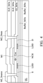
- Fig. 4 is a schematic diagram of the cross-sectional structure of a thin-film transistor included in a multiplexer in accordance with some embodiments of the disclosure.
- the TFT in the multiplexer may be formed on the glass substrate GL, the TFT may include, but us not limited to, a silicon nitride buffer layer Buffer _SiNx, a silicon oxide buffer layer Buffer_SiOx, a semiconductor layer (including a source S, a drain D, a channel layer NCH, and a lightly doped layer LDD), a gate insulating layer GI_SiOx, a silicon nitride interlayer dielectric layer ILD_SiNx, and a silicon oxide interlayer dielectric layer ILD_SiOx.
- a silicon nitride buffer layer Buffer _SiNx a silicon oxide buffer layer Buffer_SiOx
- a semiconductor layer including a source S, a drain D, a channel layer NCH, and a lightly
- the source S, the drain D, the channel layer NCH, and the lightly doped layer LDD are formed between the silicon oxide buffer layer Buffer_SiOx and the gate insulating layer GI_SiOx.
- the TFT may also include a source electrode M2_Source, which is electrically connected to the source S of the TFT, and a drain electrode M2_Drain, which is electrically connected to the drain D of the TFT.
- the metal layer M1 forms the gate the TFT.
- the parasitic capacitance Cox is formed at the polysilicon material between the metal layer M1 and the channel layer NCH (for example, the gate insulating layer GI_SiOx).
- the gate of the TFT may be located under the channel layer NCH, or a single TFT contains multiple gates.
- the TFTs in the first multiplexer 204 and the second multiplexer 206 are turned off. Affected by the difference in the number of sub-pixels connected to the first data line 210 and the second data line 212 individually, and the parasitic capacitance Cox of the TFT in the multiplexer shown in Fig. 4 , the feed-through effect generated by the first multiplexer 204 and the second multiplexer 206 after being turned off may be inconsistent, resulting in abnormal display of the display device 100.
- the size of the multiplexer is related to the channel length and channel width of the TFT. Please refer to Fig. 1 , Fig. 2 , Fig. 4 , and Fig. 5.
- Fig. 5 is a schematic diagram of the channel width of the thin-film transistor included in the multiplexer in accordance with some embodiments of the disclosure. More specifically, the TFT 500 shown in Fig. 5 may represent a schematic diagram of the layout of the TFT included in the second multiplexer 206 in Fig. 2 , and the TFT 502 may represent a schematic diagram of the layout of the TFT included in the first multiplexer 204 in Fig. 2 . In Fig.
- the channel length of the TFT 500 in the second multiplexer 206 is L, and the channel width is W1.
- the channel length of the TFT 502 in the first multiplexer 204 is also L, and the channel width is W2.
- the channel width W2 is less than the channel width W1.
- the size of the first multiplexer may be defined as W2/L
- the size of the second multiplexer may be defined as W1/L.
- the second multiplexer 206 corresponding to the TFT 500 is electrically connected to the second data line 103 corresponding to the point B in the second display area 104 of Fig. 1 .
- the first multiplexer 204 corresponding to the TFT 502 is electrically connected to the first data line 101 corresponding to the point A in the first display area 102 of Fig. 1 .
- the present disclosure adjusts the channel width of the TFTs included in different multiplexers in different display areas to adjust the feed-through effect caused by the parasitic capacitance Cox in different TFTs.
- the present disclosure reduces the uneven display quality caused by the inconsistency of the feed-through effect when the corresponding multiplexer is turned on and off in different display areas.
- the channel width W1 of the TFT 500 in the second multiplexer 206 is set as 50 ⁇ m
- the channel width W2 of the TFT 502 in the first multiplexer 204 is set as 20 ⁇ m.
- the source driver 214 in Fig. 2 provides a 6V voltage to charge the sub-pixels electrically connected to the second multiplexer 206, so that a 5.96061V voltage (referred to as the third voltage) may be measured on the drain D (where it is electrically connected to the sub-pixels through the second data line 212) of the TFT 500 in the second multiplexer 206.
- a 5.88505V voltage (referred to as the fourth voltage) may be measured on the drain D of the TFT 500.
- the source driver 214 in Fig. 2 provides a 6V voltage to charge the sub-pixels electrically connected to the first multiplexer 204, so that a 5.97581V voltage (referred to as the first voltage) may be measured on the drain D (where it is electrically connected to the sub-pixels through the second data line 210) of the TFT 502 in the first multiplexer 204.
- a 5.89706V voltage (referred to as the second voltage) may be measured on the drain D of the TFT 502.
- the feed-through effects of the first multiplexer 204 and the second multiplexer 206 may be regarded as substantially the same.
- the channel width W1 of the TFT 500 in the second multiplexer 206 is still set as 50 ⁇ m, and the channel width W2 of the TFT 502 in the first multiplexer 204 is amended from 20 ⁇ m to 50 ⁇ m, so that the channel width W2 is the same as the channel width W1.
- the source driver 214 in Fig. 2 provides a 6V voltage to charge the sub-pixels electrically connected to the first multiplexer 204, so that a 5.99868V voltage (referred to as the first voltage) may be measured on the drain D of the TFT 502.
- a 5.82734V voltage (referred to as the second voltage) may be measured on the drain D of the TFT 502.
- the feed-through effect of the first multiplexer 204 is quite close to the feed-through effect of the second multiplexer 206.
- the feed-through effect of the first multiplexer 204 is increased to about twice the feed-through effect of the second multiplexer 206.
- the first multiplexer 204 corresponding to fewer sub-pixels still maintains the same TFT channel width as the second multiplexer 206 corresponding to more sub-pixels (that is, when the size of the multiplexers is the same)
- the feed-through effect caused by the parasitic capacitance Cox in the TFT 502 of the first multiplexer 204 may be more serious.
- the feed-through effects of the first multiplexer 204 and the second multiplexer 206 may be regarded as inconsistent. It should be noted that the above result is an example. In this disclosure, the size of the TFT and the feed-through effect of each multiplexer may be different depending on the actual product.
- M' is the size of the first multiplexer 204
- M is the size of the second multiplexer 206.
- a is a size conversion constant.
- k is a pixel scale constant.
- p ' is the number if sub-pixels electrically connected by the first multiplexer 204 through the first data line (such as the data line 210).
- N is a parameter for selection, and is a positive integer from 1 to 10 (1 ⁇ N ⁇ 10).
- P max is the number of sub-pixels electrically connected by the second multiplexer 206 through the second data line 212.
- the number of sub-pixels electrically connected to the second data line 212 is the maximum of the number of sub-pixels electrically connected to all the second data lines in the second display area 104, but the present disclosure is not limited thereto.
- the size of the multiplexer is related to the channel width of the TFT in Fig. 5 (for example, the channel width W2 of the TFT 502 of the first multiplexer 204 and the channel width W1 of the TFT 500 of the second multiplexer 206), but the present disclosure is not limited thereto.
- the channel width W1 of the TFT 500 included in the second multiplexer 206 is set to 50 ⁇ m.
- the present disclosure defines the point A' between the point A and the point B in Fig. 1 to divide the first display area 102 and the second display area 104.
- the point A is located in the first display area 102, and the point B is located in the second display area 104.
- the point A" may also be defined in a similar manner, so that the number of sub-pixels electrically connected to any one of the first data lines between the point A'(or the point A") and the side edge of the display device 100 (that is, the first display area 102) is less than the number of sub-pixels electrically connected to any of the second data lines in the second display area. It should be noted that, in some embodiments, the present disclosure does not limit the division of the display device 100 into two display areas, and the display device 100 may also be divided into more display areas.
- equations 1 to 3 may still be used to estimate the size of the corresponding multiplexer in each display area.
- the appearance of the display panel of the display device may cause the sub-pixels electrically connected to each data line to be different.
- the size conversion constant a is equal to 0.51.
- the size conversion constant a is equal to 0.24.
- the size conversion constant a is between 0.13 and 1 (0.13 ⁇ a ⁇ 1).
- the size of the multiplexer in the second display area may be set according to actual requirements (such as customer specifications), for example, the channel width W1 of the TFT 500 in the second multiplexer 206 is set as 50 ⁇ m, and the recommended values of the channel width W2 of the TFT 502 in the first multiplexer 204 are 38 ⁇ m, 31 ⁇ m, 26 ⁇ m, 23 ⁇ m, 20 ⁇ m, 18 ⁇ m, 16 ⁇ m, 14 ⁇ m, 13 ⁇ m, and 12 ⁇ m.
- the present disclosure inputs the above recommended values into a semiconductor simulation software to simulate that when the channel width W2 of the TFT 502 of the first multiplexer 204 and the channel width W1 of the TFT 500 of the second multiplexer 206 are maintained at 50 ⁇ m, one of the recommended values, which makes the feed-through effect of the first multiplexer 204 the closest to the feed-through effect of the second multiplexer 206, is set as the channel width W2 of the TFT 502 of the first multiplexer 204.
- the above result is an example, and the size of the TFT and the feed-through effect of each multiplexer in the present disclosure may be different depending on the actual product.
- Fig. 3 is a schematic diagram of the peripheral areas in accordance with some embodiments of the disclosure.
- the difference between each multiplexer in the multiplexer group 300 in Fig. 3 and the first multiplexers 202 and 204 and the second multiplexer 206 in Fig. 2 is that each multiplexer in the multiplexer group 300 in Fig. 3 may include a plurality of TFTs.
- the first multiplexer in Fig. 3 may include n TFTs 202-1, 202-2,..., 202-n in parallel with each other to replace the first multiplexer 202 in Fig. 2 .
- n and m are positive integers greater than or equal to 2, and n and m may be the same or different.
- the sources of the TFTs 202-1, 202-2,..., 202-n, 204-1, 204-2,..., 204-n, 206-1, 206-2,..., 206-m are all electrically connected to the source driver 214, but the present disclosure is not limited thereto. In some embodiments, due to considerations during the design of the display device (for example, factors such as the size or appearance of the display device), different multiplexers may be electrically connected to different source drivers.
- the size of a single multiplexer is adjusted by the number of parallel TFTs. Since the size of multiplexers may be superimposed through parallel connection of TFTs, when the size of each TFT is approximately the same, and the number of TFTs corresponding to the first multiplexer is less than the number of TFTs corresponding to the second multiplexer (n ⁇ m), the size of the first multiplexer may be made smaller than that of the second multiplexer.
- the size of the multiplexer may be adjusted by adjusting the number of parallel TFTs. For example, the present disclosure makes the size of the first multiplexer smaller than the size of the second multiplexer to reduce the impact on the image quality due to inconsistent feed-through effects.
- Fig. 6A is a waveform diagram of the first multiplexer 204 before channel width adjustment in accordance with some embodiments of the disclosure.
- Fig. 6B is a waveform diagram of the second multiplexer 206 in accordance with some embodiments of the disclosure.
- the channel widths W1 and W2 in the first multiplexer 204 and the second multiplexer 206 may be, for example, 50 ⁇ m, respectively.
- the waveform curve 600 is the waveform measured at the gate G of the TFT 502 in the first multiplexer 204.
- Fig. 6A is the waveform measured at the gate G of the TFT 502 in the first multiplexer 204.
- the waveform curve 606 is the waveform measured at the gate G of the TFT 500 in the second multiplexer 206.
- the waveform curves 600 and 606 may be the waveform diagram of the control signal group MUXCKH in Fig. 1 or the waveform diagram of the control signals CKH[1], CKH[2] and CKH[3] in Fig. 2 and so on.
- the waveform curve 602 is the waveform measured on the drain D of the TFT 502 in the first multiplexer 204
- the waveform curve 608 is the waveform measured on the drain D of the TFT 500 in the second multiplexer 206.
- the waveform curve 600 (the control signal CKH[2] in Fig. 2 ) changes from a low level to a high level
- the TFT 502 in the first multiplexer 204 is turned on, the source driver 214 in Fig. 2 charges the sub-pixel (for example, the sub-pixel 218 in Fig. 2 ) electrically connected to the TFT 502 of the first multiplexer 204 to a voltage V1. Therefore, the waveform curve 602 may be measured on the drain D of the TFT 502 of the first multiplexer 204.
- the waveform 606 (the control signal CKH[3] in Fig.
- the TFT 500 in the first multiplexer 206 changes from a low level to a high level, the TFT 500 in the first multiplexer 206 is turned on, the source driver 214 in Fig. 2 charges the sub-pixel (for example, the sub-pixel 220 in Fig. 2 ) electrically connected to the TFT 500 of the first multiplexer 206 to a voltage V3. Therefore, the waveform curve 608 may be measured on the drain D of the TFT 500 of the first multiplexer 206.
- the waveform curve 602 corresponding to the first multiplexer may generate a more obvious voltage fluctuation (feed-through effect) like the voltage drop 604, and after the voltage drop 604, the waveform curve 602 may return back to the voltage V2. It can be seen from Fig. 6A that the voltage V2 is lower than the voltage V1. In Fig. 6B , the voltage fluctuation of the waveform curve 608 corresponding to the second multiplexer is relatively small, the waveform curve 608 may change from the voltage V3 to the voltage V4, and the voltage V4 is lower than the voltage V3.
- the channel width of the TFT 502 in the first multiplexer 204 is adjusted to, for example, 20 ⁇ m, it may be seen from the foregoing description that the feed-through effect of the first multiplexer 204 and the feed-through effect of the second multiplexer 206 may be regarded as substantially the same at this time. Therefore, after adjustment, the waveform measured on the first multiplexer 204 may be close to the waveform 608 of the second multiplexer 206 shown in Fig. 6B .
- the voltage gap before and after the voltage fluctuation may be small (for example, (V3-V4) ⁇ (V1-V2)), but the present disclosure is not limited thereto.
- the present disclosure divides the display panel of a non-rectangular display device, and designs different multiplexer sizes in different display areas (for example, different channel widths in TFT) to improve the display abnormalities caused by the inconsistent feed-through effect in the display device.
Landscapes
- Physics & Mathematics (AREA)
- Engineering & Computer Science (AREA)
- General Physics & Mathematics (AREA)
- Nonlinear Science (AREA)
- Theoretical Computer Science (AREA)
- Computer Hardware Design (AREA)
- Chemical & Material Sciences (AREA)
- Crystallography & Structural Chemistry (AREA)
- Mathematical Physics (AREA)
- Optics & Photonics (AREA)
- Microelectronics & Electronic Packaging (AREA)
- Devices For Indicating Variable Information By Combining Individual Elements (AREA)
- Liquid Crystal (AREA)
- Thin Film Transistor (AREA)
Abstract
Description
- This application claims priority to and the benefit of
China Application No. 202010690331.8, filed on July 17th, 2020 - The disclosure is related to a display device, and in particular it is related to a display area than can improve the feed-through effect of the multiplexer in the display area.
- In a non-rectangular (free shape) display panel, the number of sub-pixels connected to data lines in different positions in the display area may be different, which makes the load (RC loading) of the data lines in different positions in the display area different. At this moment, the parasitic capacitance of the multiplexer (MUX) inside the panel may affect the charging of the corresponding sub-pixels, so that the data line with a small number of sub-pixels may suffer a greater feed-through effect, and the inconsistency of the feed-through effect may affect the display quality.
- In order to resolve the issue described above, the present disclose provides a display device. The display device includes a first display area, a second display area, a first multiplexer, and a second multiplexer. The first display area includes a plurality of first data lines. The second display area is adjacent to the first display area, and includes a plurality of second data lines. The first multiplexer is electrically connected to one of the first data lines. The second multiplexer is electrically connected to one of the second data lines. The first data line is electrically connected to a first number of sub-pixels. The second data line is electrically connected to a second number of sub-pixels. The first number is less than the second number. The size of the first multiplexer is smaller than that of the second multiplexer.
- The disclosure can be more fully understood by reading the subsequent detailed description with references made to the accompanying figures. It should be understood that the figures are not drawn to scale in accordance with standard practice in the industry. In fact, it is allowed to arbitrarily enlarge or reduce the size of components for clear illustration. This means that many special details, relationships and methods are disclosed to provide a complete understanding of the disclosure.
-
Fig. 1 is a schematic diagram of a display device in accordance with some embodiments of the disclosure. -
Fig. 2 is a schematic diagram of a first display area, a second display area and peripheral areas inFig. 1 in accordance with some embodiments of the disclosure. -
Fig. 3 is a schematic diagram of the peripheral areas in accordance with some embodiments of the disclosure. -
Fig. 4 is a schematic diagram of the cross-sectional structure of a thin-film transistor included in a multiplexer in accordance with some embodiments of the disclosure. -
Fig. 5 is a schematic diagram of the channel width of the thin-film transistor included in the multiplexer in accordance with some embodiments of the disclosure. -
Fig. 6A is a waveform diagram of the first multiplexer before channel width adjustment in accordance with some embodiments of the disclosure. -
Fig. 6B is a waveform diagram of the second multiplexer in accordance with some embodiments of the disclosure. - In order to make the above purposes, features, and advantages of some embodiments of the present disclosure more comprehensible, the following is a detailed description in conjunction with the accompanying drawings.
- Certain terms are used throughout the description and following claims to refer to particular components. As one skilled in the art will understand, electronic equipment manufacturers may refer to a component by different names. This document does not intend to distinguish between components that differ in name but not function. It should be understood that the words "comprise", "have" and "include" are used in an open-ended fashion, and thus should be interpreted to mean "include, but not limited to...". Thus, when the terms "comprise", "have" and/or "include" used in the present disclosure are used to indicate the existence of specific technical features, values, method steps, operations, units and/or components. However, it does not exclude that more technical features, numerical values, method steps, work processes, units, components, or any combination of the above can be added.
- The directional terms used throughout the description and following claims, such as: "on", "up", "above", "down", "below", "front", "rear", "back", "left", "right", etc., are only directions referring to the drawings. Therefore, the directional terms are used for explaining and not used for limiting the present disclosure. Regarding the drawings, the drawings show the general characteristics of methods, structures, and/or materials used in specific embodiments. However, the drawings should not be construed as defining or limiting the scope or properties encompassed by these embodiments. For example, for clarity, the relative size, thickness, and position of each layer, each area, and/or each structure may be reduced or enlarged.
- When the corresponding component such as layer or area is referred to "on another component", it may be directly on this another component, or other component(s) may exist between them. On the other hand, when the component is referred to "directly on another component (or the variant thereof)", any component does not exist between them. Furthermore, when the corresponding component is referred to "on another component", the corresponding component and another component have a disposition relationship along a top-view/vertical direction, the corresponding component may be below or above another component, and the disposition relationship along the top-view/vertical direction are determined by an orientation of the device.
- It will be understood that when a component or layer is referred to as being "connected to" another component or layer, it can be directly connected to this another component or layer, or intervening components or layers may be presented. In contrast, when a component is referred to as being "directly connected to" another component or layer, there are no intervening components or layers presented.
- The electrical connection or coupling described in this disclosure may refer to direct connection or indirect connection. In the case of direct connection, the endpoints of the components on the two circuits are directly connected or connected to each other by a conductor line segment, while in the case of indirectly connected, there are switches, diodes, capacitors, inductors, resistors, other suitable components, or a combination of the above components between the endpoints of the components on the two circuits, but the intermediate component is not limited thereto.
- The words "first", "second", "third", "fourth", "fifth", and "sixth" are used to describe components, they are not used to indicate the priority order of or advance relationship, but only to distinguish components with the same name.
- It should be noted that the technical features in different embodiments described in the following can be replaced, recombined, or mixed with one another to constitute another embodiment without departing from the spirit of the present disclosure.
- In the present disclosure, the display device can be any suitable type of display device or electronic device with a display panel, such as a touch display, an antenna device, a splicing device, a sensing device, a flexible device, etc., but the present is not limited thereto. The electronic device described in the present disclosure may be a touch display integrated with touch and display functions, and the display panel may include liquid crystal (LC), organic light-emitting diode (OLED), inorganic light-emitting diode (light-emitting diode, LED) such as micro-LED, mini-LED, sub-millimeter light-emitting diode (mini-LED), quantum dot light-emitting diode (QLED, QDLED), fluorescent material, phosphor material, quantum dots (QDs) material, other suitable materials or a combination of the above materials, but the present disclosure is not limited thereto. The splicing device may be, for example, a display splicing device or an antenna splicing device, but the present disclosure is not limited thereto. In addition, the display panel in the electronic device may be a color display panel or a monochrome display panel, and the shape of the display panel can be a rectangle, a circuit, a polygon, a shape with a curved edge, or other suitable shapes.
-
Fig. 1 is a schematic diagram of a display device in accordance with some embodiments of the disclosure. As shown inFig. 1 , thedisplay device 100 includes afirst display area 102, asecond display area 104, aperipheral area 106 where a first multiplexer is located, and aperipheral area 108 where a second multiplexer is located. Thefirst display area 102 is adjacent to thesecond display area 104. As shown inFig. 1 , in some embodiments, thefirst display area 102 are arranged on both sides of thesecond display area 104, theperipheral area 106 is adjacent to thefirst display area 102, and theperipheral area 108 is adjacent to thesecond display area 104, but the present disclosure is not limited thereto. InFig. 1 , point A' and point A" are reference points used to separate thefirst display area 102 and thesecond display area 104. The positions of point A' and point A" may correspond to the sub-pixels of the display device, but the present disclosure is not limited thereto. In some embodiments, point A' and/or point A" may be located between two adjacent sub-pixels. It should be noted that, in the present disclosure, point A' (point A") may be selected as the reference point of the boundary in the area where the appearance of the display panel of the display device begins to change significantly (for example, the junction of therectangular area 104 and the approximatelytriangular area 102 inFig. 1 ), however the appearance change of the panel disclosed in the present disclosure is not limited toFig. 1 . In some embodiments, thedisplay device 100 of the present disclosure uses the longitudinaltangent line 110 passing through point A' and extending along a Y direction (the extension direction of the display panel data line in the display device 100) inFig. 1 and the longitudinaltangent line 112 passing through point A" and extending along the Y direction inFig. 1 as the separation boundary of thefirst display area 102 and thesecond display area 104, respectively. In some embodiments, thefirst display area 102 includes a plurality of first data lines, and thesecond display area 104 includes a plurality of second data lines. - In some embodiments, in the
first display area 102, at least one of the first data lines is electrically connected to a first number of sub-pixels. In thesecond display area 104, at least one of the second data lines is electrically connected to a second number of sub-pixels. Since the display panel may be non-rectangular, in some embodiments, the first number is smaller than the second number. For example, thefirst data line 101 corresponding to point A is located in thefirst display area 102, and thesecond data line 103 corresponding to point B is located in thesecond display area 104. The number of sub-pixels electrically connected to thefirst data line 101 is less than the number of sub-pixels electrically connected to thesecond data line 103. The first multiplexer (not shown) located in theperipheral area 106 may be electrically connected to thefirst data line 101, and the second multiplexer (not shown) located in theperipheral area 108 may be electrically connected to thesecond data line 103. In some embodiments, the size of the first multiplexer is smaller than that of the second multiplexer. In some embodiments, the control signal group MUXCKH is used to respectively turn in or turn off the first multiplexer located in theperipheral area 106 and the second multiplexer located in the peripheral area 108 (more specifically, to turn on or switch the switching element in the multiplexer). -
Fig. 2 is a schematic diagram of afirst display area 102, asecond display area 104 andperipheral areas Fig. 1 in accordance with some embodiments of the disclosure. In some embodiments, the first multiplexer and the second multiplexer may each include at least one thin-film transistor (TFT). Therefore, inFig. 2 , thin-film transistors are used to represent the first multiplexer and the second multiplexer, respectively. In addition, although the present disclosure takes n-type TFTs as an example, the present disclosure is not limited thereto. In some embodiments, p-type TFTs may also be used. - In
Fig. 2 , theperipheral area 106 includes afirst multiplexer 202 and afirst multiplexer 204, and theperipheral area 108 includes asecond multiplexer 206, but the number of first multiplexers and the second multiplexers in the present disclosure is not limited thereto. Thefirst multiplexer 202, thefirst multiplexer 204 and thesecond multiplexer 206 are all electrically connected to asource driver 214, but the present disclosure is not limited thereto. In some embodiments, due to considerations during the design of the display device (such as the size or appearance of the display panel in the display device), different multiplexers are electrically connected to different source drivers. A control signal CKH[1] may be used to turn on or turn off thefirst multiplexer 202. A control signal CKH[2] may be used to turn on or turn off thefirst multiplexer 204. A control signal CKH[3] may be used to turn on or turn off thesecond multiplexer 206. In some embodiments, the control signals CKH[1], CKH[2] and CKH[3] inFig. 2 are included in the control signal group MUXCKH inFig. 1 . In some embodiments, the control signals CKH[1], CKH[2] and CKH[3] inFig. 2 and the control signal group MUXCKH inFig. 1 are from a multiplexer controller (not shown). - In
Fig. 2 , thefirst multiplexer 202 in theperipheral area 106 is electrically connected to adata line 208 in thefirst display area 102, and a sub-pixel 216 is electrically connected to thedata line 208 and ascan line 222. Thefirst multiplexer 204 is electrically connected to adata line 210, and a sub-pixel 218 is electrically connected to thedata line 210 and thescan line 222. Thesecond multiplexer 206 is electrically connected to adata line 212, and a sub-pixel 220 is electrically connected to thedata line 212 and thescan line 222. Taking thedata line 208 as an example, since the TFT in thefirst multiplexer 202 inFig. 2 is an n-type TFT, when the control signal CKH[1] changes from a low level to a high level, thefirst multiplexer 202 is turned on, and thesource driver 214 charges a storage capacitor (not shown) in the sub-pixel 216 through thedata line 208.Fig. 2 uses thedata line 208 and thedata line 210 in thefirst display area 102 respectively electrically connected to one sub-pixel (for example, the sub-pixel 216 and the sub-pixel 218) as an example. In the practical application of the present disclosure, at least one of thedata line 208 and thedata line 210 in thefirst display area 102 may be electrically connected to a first number (for example, 60) of sub-pixels, and thedata line 212 in thesecond display area 104 may be electrically connected to a second number (for example, 100) of sub-pixels. Since the number of sub-pixels connected to the data lines in different display areas may be different, the load of the data lines in different display areas may also be different. At this moment, the parasitic capacitance of the multiplexer in the display device may affect the charging of the corresponding sub-pixels, so that the data lines that are electrically connected to a small number of sub-pixels may suffer a greater feed-through effect (sudden drop in driving voltage). The inconsistency of the feed-through effect may affect the display quality. At this time, by adjusting the size of the multiplexer, for example, making the size of the first multiplexer smaller than the size of the second multiplexer, the parasitic capacitance of the multiplexer may be changed, and the impact of the inconsistency of the feed-through effect on the image quality may be reduced. -
Fig. 4 is a schematic diagram of the cross-sectional structure of a thin-film transistor included in a multiplexer in accordance with some embodiments of the disclosure. As shown inFig. 4 , the TFT in the multiplexer may be formed on the glass substrate GL, the TFT may include, but us not limited to, a silicon nitride buffer layer Buffer _SiNx, a silicon oxide buffer layer Buffer_SiOx, a semiconductor layer (including a source S, a drain D, a channel layer NCH, and a lightly doped layer LDD), a gate insulating layer GI_SiOx, a silicon nitride interlayer dielectric layer ILD_SiNx, and a silicon oxide interlayer dielectric layer ILD_SiOx. The source S, the drain D, the channel layer NCH, and the lightly doped layer LDD are formed between the silicon oxide buffer layer Buffer_SiOx and the gate insulating layer GI_SiOx. Moreover, the TFT may also include a source electrode M2_Source, which is electrically connected to the source S of the TFT, and a drain electrode M2_Drain, which is electrically connected to the drain D of the TFT. The metal layer M1 forms the gate the TFT. As shown inFig. 4 , the parasitic capacitance Cox is formed at the polysilicon material between the metal layer M1 and the channel layer NCH (for example, the gate insulating layer GI_SiOx). It should be noted that the structure and material of the TFT shown inFig. 4 is an example, but the present disclosure is not limited thereto. For example, in some embodiments, the gate of the TFT may be located under the channel layer NCH, or a single TFT contains multiple gates. - Referring to
Fig. 1 ,Fig. 2 , andFig. 4 at the same time, and taking thefirst multiplexer 204 and thesecond multiplexer 206 inFig. 2 as an example, when the control signal CKH[2] and the control signal CKH[3] changes from a high level to a low level, the TFTs in thefirst multiplexer 204 and thesecond multiplexer 206 are turned off. Affected by the difference in the number of sub-pixels connected to thefirst data line 210 and thesecond data line 212 individually, and the parasitic capacitance Cox of the TFT in the multiplexer shown inFig. 4 , the feed-through effect generated by thefirst multiplexer 204 and thesecond multiplexer 206 after being turned off may be inconsistent, resulting in abnormal display of thedisplay device 100. - The size of the multiplexer is related to the channel length and channel width of the TFT. Please refer to
Fig. 1 ,Fig. 2 ,Fig. 4 , andFig. 5. Fig. 5 is a schematic diagram of the channel width of the thin-film transistor included in the multiplexer in accordance with some embodiments of the disclosure. More specifically, theTFT 500 shown inFig. 5 may represent a schematic diagram of the layout of the TFT included in thesecond multiplexer 206 inFig. 2 , and theTFT 502 may represent a schematic diagram of the layout of the TFT included in thefirst multiplexer 204 inFig. 2 . InFig. 5 , the channel length of theTFT 500 in thesecond multiplexer 206 is L, and the channel width is W1. The channel length of theTFT 502 in thefirst multiplexer 204 is also L, and the channel width is W2. The channel width W2 is less than the channel width W1. At this time, the size of the first multiplexer may be defined as W2/L, and the size of the second multiplexer may be defined as W1/L. It should be noted that the schematic diagram of the layout of the TFT inFig. 5 is an example for convenience of explanation, and the method of defining the channel length and channel width may vary according to the actual structure. The shaded area inFig. 5 is the lightly doped layer LDD inFig. 4 . The source S inFig. 5 may correspond to the source S inFig. 4 . The drain D inFig. 5 may correspond to the drain D inFig. 4 . In some embodiments, thesecond multiplexer 206 corresponding to theTFT 500 is electrically connected to thesecond data line 103 corresponding to the point B in thesecond display area 104 ofFig. 1 . Thefirst multiplexer 204 corresponding to theTFT 502 is electrically connected to thefirst data line 101 corresponding to the point A in thefirst display area 102 ofFig. 1 . - As described above, the present disclosure adjusts the channel width of the TFTs included in different multiplexers in different display areas to adjust the feed-through effect caused by the parasitic capacitance Cox in different TFTs. The present disclosure reduces the uneven display quality caused by the inconsistency of the feed-through effect when the corresponding multiplexer is turned on and off in different display areas.
- For example, please refer to
Fig. 2 andFig. 5 at the same time, in some embodiments, the channel width W1 of theTFT 500 in thesecond multiplexer 206 is set as 50 µm, and the channel width W2 of theTFT 502 in thefirst multiplexer 204 is set as 20µ m. When thesecond multiplexer 206 is turned on, thesource driver 214 inFig. 2 provides a 6V voltage to charge the sub-pixels electrically connected to thesecond multiplexer 206, so that a 5.96061V voltage (referred to as the third voltage) may be measured on the drain D (where it is electrically connected to the sub-pixels through the second data line 212) of theTFT 500 in thesecond multiplexer 206. When thesecond multiplexer 206 is turned off, a 5.88505V voltage (referred to as the fourth voltage) may be measured on the drain D of theTFT 500. Similarly, when thefirst multiplexer 204 is turned on, thesource driver 214 inFig. 2 provides a 6V voltage to charge the sub-pixels electrically connected to thefirst multiplexer 204, so that a 5.97581V voltage (referred to as the first voltage) may be measured on the drain D (where it is electrically connected to the sub-pixels through the second data line 210) of theTFT 502 in thefirst multiplexer 204. When thefirst multiplexer 204 is turned off, a 5.89706V voltage (referred to as the second voltage) may be measured on the drain D of theTFT 502. According to the above measurement data, in this measurement, the feed-through effect in the first multiplexer 204 (5.97581V-5.89706V=0.07875V) is quite close to the feed-through effect in the second multiplexer 206 (5.96061V-5.8805V=0.08011V). At this time, the feed-through effects of thefirst multiplexer 204 and thesecond multiplexer 206 may be regarded as substantially the same. - In addition, the channel width W1 of the
TFT 500 in thesecond multiplexer 206 is still set as 50 µm, and the channel width W2 of theTFT 502 in thefirst multiplexer 204 is amended from 20 µm to 50 µm, so that the channel width W2 is the same as the channel width W1. When thefirst multiplexer 204 is turned on, thesource driver 214 inFig. 2 provides a 6V voltage to charge the sub-pixels electrically connected to thefirst multiplexer 204, so that a 5.99868V voltage (referred to as the first voltage) may be measured on the drain D of theTFT 502. When thefirst multiplexer 204 is turned off, a 5.82734V voltage (referred to as the second voltage) may be measured on the drain D of theTFT 502. At this time, the feed-through effect of thefirst multiplexer 204 increases to 0.17134V(5.99868V-5.82734V=0.17134V). according to the above data, when the channel width W2 of theTFT 502 of thefirst multiplexer 204 is 20 µm, and the channel width W1 of theTFT 500 of thesecond multiplexer 206 is 50 µm, the feed-through effect of thefirst multiplexer 204 is quite close to the feed-through effect of thesecond multiplexer 206. However, when the channel width W2 of theTFT 502 of thefirst multiplexer 204 is 50 µm (equal to the channel width W1 of theTFT 500 of the second multiplexer 206), the feed-through effect of thefirst multiplexer 204 is increased to about twice the feed-through effect of thesecond multiplexer 206. In other words, when thefirst multiplexer 204 corresponding to fewer sub-pixels still maintains the same TFT channel width as thesecond multiplexer 206 corresponding to more sub-pixels (that is, when the size of the multiplexers is the same), the feed-through effect caused by the parasitic capacitance Cox in theTFT 502 of thefirst multiplexer 204 may be more serious. At this time, the feed-through effects of thefirst multiplexer 204 and thesecond multiplexer 206 may be regarded as inconsistent. It should be noted that the above result is an example. In this disclosure, the size of the TFT and the feed-through effect of each multiplexer may be different depending on the actual product. - Please refer to
Fig. 2 andFig. 5 . In some embodiments, in order to reduce the inconsistency of the feed-through effect caused by different factor pixels, the size of different multiplexers may have the following relationship:


- M' is the size of the
first multiplexer 204, M is the size of thesecond multiplexer 206. a is a size conversion constant. k is a pixel scale constant. p'is the number if sub-pixels electrically connected by thefirst multiplexer 204 through the first data line (such as the data line 210). N is a parameter for selection, and is a positive integer from 1 to 10 (1≤ N≤ 10). Pmax is the number of sub-pixels electrically connected by thesecond multiplexer 206 through thesecond data line 212. In some embodiments, the number of sub-pixels electrically connected to thesecond data line 212 is the maximum of the number of sub-pixels electrically connected to all the second data lines in thesecond display area 104, but the present disclosure is not limited thereto. - For example, in the embodiment of
Fig. 5 , the size of the multiplexer is related to the channel width of the TFT inFig. 5 (for example, the channel width W2 of theTFT 502 of thefirst multiplexer 204 and the channel width W1 of theTFT 500 of the second multiplexer 206), but the present disclosure is not limited thereto. Please refer toFig. 1 ,Fig. 2 andFig. 5 at the same time. When the channel lengths are all L, first, the channel width W1 of theTFT 500 included in thesecond multiplexer 206 is set to 50 µm. The present disclosure defines the point A' between the point A and the point B inFig. 1 to divide thefirst display area 102 and thesecond display area 104. At this time, the point A is located in thefirst display area 102, and the point B is located in thesecond display area 104. In addition, the point A" may also be defined in a similar manner, so that the number of sub-pixels electrically connected to any one of the first data lines between the point A'(or the point A") and the side edge of the display device 100 (that is, the first display area 102) is less than the number of sub-pixels electrically connected to any of the second data lines in the second display area. It should be noted that, in some embodiments, the present disclosure does not limit the division of thedisplay device 100 into two display areas, and thedisplay device 100 may also be divided into more display areas. However,equations 1 to 3 may still be used to estimate the size of the corresponding multiplexer in each display area. In some embodiments, the appearance of the display panel of the display device may cause the sub-pixels electrically connected to each data line to be different. At this time,equations 1 ~ 3 may still be used to estimate the size of the multiplexer corresponding to each data line. For example, when the number of sub-pixels electrically connected to thefirst data line 101 corresponding to the point A is 247, and the number of sub-pixels electrically connected to thesecond data line 103 corresponding to the point B is 392, p'=247 and Pmax =392 is substituted intoequation 3, and the pixel scale constant k equal to 0.63 is obtained. - Then, the present disclosure substitutes k =0.63 and N=1~10 into
equation 2 respectively, and when N=1, the size conversion constant a is equal to 0.763. When N=2, the size conversion constant a is equal to 0.617. When N=3, the size conversion constant a is equal to 0.51. When N=4, the size conversion constant a is equal to 0.45. When N=5, the size conversion constant a is equal to 0.392. When N=6, the size conversion constant a is equal to 0.35. When N=7, the size conversion constant a is equal to 0.315. When N=8, the size conversion constant a is equal to 0.287. When N=9, the size conversion constant a is equal to 0.263. When N=10, the size conversion constant a is equal to 0.24. Generally, the size conversion constant a is between 0.13 and 1 (0.13 ≤ a ≤ 1). After that, the present disclosure substitutes each size conversion constant a obtained under the condition of N=1~10 intoequation 1. At this time, the size of the multiplexer in the second display area may be set according to actual requirements (such as customer specifications), for example, the channel width W1 of theTFT 500 in thesecond multiplexer 206 is set as 50µm, and the recommended values of the channel width W2 of theTFT 502 in thefirst multiplexer 204 are 38 µm, 31µm, 26µm, 23µm, 20µm, 18µm, 16µm, 14µm, 13µm, and 12 µm. - Finally, the present disclosure inputs the above recommended values into a semiconductor simulation software to simulate that when the channel width W2 of the
TFT 502 of thefirst multiplexer 204 and the channel width W1 of theTFT 500 of thesecond multiplexer 206 are maintained at 50 µm, one of the recommended values, which makes the feed-through effect of thefirst multiplexer 204 the closest to the feed-through effect of thesecond multiplexer 206, is set as the channel width W2 of theTFT 502 of thefirst multiplexer 204. It should be noted that the above result is an example, and the size of the TFT and the feed-through effect of each multiplexer in the present disclosure may be different depending on the actual product. - Please refer to
Fig. 3. Fig. 3 is a schematic diagram of the peripheral areas in accordance with some embodiments of the disclosure. The difference between each multiplexer in themultiplexer group 300 inFig. 3 and thefirst multiplexers second multiplexer 206 inFig. 2 is that each multiplexer in themultiplexer group 300 inFig. 3 may include a plurality of TFTs. For example, the first multiplexer inFig. 3 may include n TFTs 202-1, 202-2,..., 202-n in parallel with each other to replace thefirst multiplexer 202 inFig. 2 . Similarly, the second multiplexer inFig. 3 may include m TFTs 206-1, 206-2,..., 206-m in parallel with each other to replace thesecond multiplexer 206 inFig. 2 , and the remaining first multiplexer and second multiplexer may be analogized. n and m are positive integers greater than or equal to 2, and n and m may be the same or different. The sources of the TFTs 202-1, 202-2,..., 202-n, 204-1, 204-2,..., 204-n, 206-1, 206-2,..., 206-m are all electrically connected to thesource driver 214, but the present disclosure is not limited thereto. In some embodiments, due to considerations during the design of the display device (for example, factors such as the size or appearance of the display device), different multiplexers may be electrically connected to different source drivers. - The difference between the above embodiment and the embodiment in
Fig. 2 is that the size of a single multiplexer is adjusted by the number of parallel TFTs. Since the size of multiplexers may be superimposed through parallel connection of TFTs, when the size of each TFT is approximately the same, and the number of TFTs corresponding to the first multiplexer is less than the number of TFTs corresponding to the second multiplexer (n<m), the size of the first multiplexer may be made smaller than that of the second multiplexer. - As mentioned above, since the number of sub-pixels electrically connected to the data lines in different display areas may be different, the load of the data lines in different display areas may be different. At this time, the parasitic capacitance of the multiplexer in the display device may affect the charging of the corresponding sub-pixels, so that the data line with a small number of sub-pixels may suffer a greater feed-through effect, and the inconsistency of the feed-through effect may affect the display quality. At this time, the size of the multiplexer may be adjusted by adjusting the number of parallel TFTs. For example, the present disclosure makes the size of the first multiplexer smaller than the size of the second multiplexer to reduce the impact on the image quality due to inconsistent feed-through effects.
- Please refer to
Fig. 2 ,Fig. 5 ,Fig. 6A and Fig. 6B. Fig. 6A is a waveform diagram of thefirst multiplexer 204 before channel width adjustment in accordance with some embodiments of the disclosure.Fig. 6B is a waveform diagram of thesecond multiplexer 206 in accordance with some embodiments of the disclosure. In some embodiments, the channel widths W1 and W2 in thefirst multiplexer 204 and thesecond multiplexer 206 may be, for example, 50 µm, respectively. As shown inFig. 6A , thewaveform curve 600 is the waveform measured at the gate G of theTFT 502 in thefirst multiplexer 204. As shown inFig. 6B , thewaveform curve 606 is the waveform measured at the gate G of theTFT 500 in thesecond multiplexer 206. In some embodiments, the waveform curves 600 and 606 may be the waveform diagram of the control signal group MUXCKH inFig. 1 or the waveform diagram of the control signals CKH[1], CKH[2] and CKH[3] inFig. 2 and so on. Thewaveform curve 602 is the waveform measured on the drain D of theTFT 502 in thefirst multiplexer 204, and thewaveform curve 608 is the waveform measured on the drain D of theTFT 500 in thesecond multiplexer 206. - When the waveform curve 600 (the control signal CKH[2] in
Fig. 2 ) changes from a low level to a high level, theTFT 502 in thefirst multiplexer 204 is turned on, thesource driver 214 inFig. 2 charges the sub-pixel (for example, the sub-pixel 218 inFig. 2 ) electrically connected to theTFT 502 of thefirst multiplexer 204 to a voltage V1. Therefore, thewaveform curve 602 may be measured on the drain D of theTFT 502 of thefirst multiplexer 204. Similarly, when the waveform 606 (the control signal CKH[3] inFig. 2 ) changes from a low level to a high level, theTFT 500 in thefirst multiplexer 206 is turned on, thesource driver 214 inFig. 2 charges the sub-pixel (for example, the sub-pixel 220 inFig. 2 ) electrically connected to theTFT 500 of thefirst multiplexer 206 to a voltage V3. Therefore, thewaveform curve 608 may be measured on the drain D of theTFT 500 of thefirst multiplexer 206. Due to the difference in the number of sub-pixels corresponding to thefirst multiplexer 204 and thesecond multiplexer 206, when the control signal changes from the high level the low level, and the size of thefirst multiplexer 204 and thesecond multiplexer 206 are the same, thewaveform curve 602 corresponding to the first multiplexer may generate a more obvious voltage fluctuation (feed-through effect) like thevoltage drop 604, and after thevoltage drop 604, thewaveform curve 602 may return back to the voltage V2. It can be seen fromFig. 6A that the voltage V2 is lower than the voltage V1. InFig. 6B , the voltage fluctuation of thewaveform curve 608 corresponding to the second multiplexer is relatively small, thewaveform curve 608 may change from the voltage V3 to the voltage V4, and the voltage V4 is lower than the voltage V3. - When the channel width of the
TFT 502 in thefirst multiplexer 204 is adjusted to, for example, 20 µm, it may be seen from the foregoing description that the feed-through effect of thefirst multiplexer 204 and the feed-through effect of thesecond multiplexer 206 may be regarded as substantially the same at this time. Therefore, after adjustment, the waveform measured on thefirst multiplexer 204 may be close to thewaveform 608 of thesecond multiplexer 206 shown inFig. 6B . In addition, as shown inFigs. 6A and 6B , in some embodiments, when the feed-through effect is small, the voltage gap before and after the voltage fluctuation may be small (for example, (V3-V4)<(V1-V2)), but the present disclosure is not limited thereto. - In summary, the present disclosure divides the display panel of a non-rectangular display device, and designs different multiplexer sizes in different display areas (for example, different channel widths in TFT) to improve the display abnormalities caused by the inconsistent feed-through effect in the display device.
- The embodiments of the present disclosure are disclosed above, but they are not used to limit the scope of the present disclosure. A person skilled in the art can make some changes and retouches without departing from the spirit and scope of the embodiments of the present disclosure. Therefore, the scope of protection in the present disclosure shall be deemed as defined by the scope of the attached claims.
Claims (15)
- A display device (100), comprising:a first display area (102), comprising a plurality of first data lines (101);a second display area (104), adjacent to the first display area and comprising a plurality of second data lines (103);a first multiplexer (106), electrically connected to one of the first data lines;a second multiplexer (108), electrically connected to one of the second data lines;wherein the one of the first data lines (101) is electrically connected to a first number of sub-pixels, the one of the second data lines (103) is electrically connected to a second number of sub-pixels, the first number is less than the second number, and a size of the first multiplexer (106) is smaller than that of the second multiplexer (108).
- The display device (100) as claimed in claim 1, wherein the first multiplexer (106) comprises at least one thin-film transistor (TFT), and the second multiplexer (108) includes at least one TFT.
- The display device (100) as claimed in claim 2, wherein a channel width of the at least one TFT of the first multiplexer (106) is less than that of the at least one TFT of the second multiplexer (108), and/or wherein the first multiplexer (106) comprises n TFTs, the second multiplexer (108) comprises m TFTs, n and m are positive integers, and n is less than m.
- The display device (100) as claimed in one of the preceding claims, wherein a first control signal (CKH[1]) is used to turn on or turn off the first multiplexer (106), and a second control signal (CKH[2]) is used to turn on or turn off the second multiplexer (108).
- The display device (100) as claimed in one of the preceding claims, wherein the first multiplexer (106) is located in a first peripheral area, and the first peripheral area is adjacent to the first display area (102); the second multiplexer (108) is located in a second peripheral area, and the second peripheral area is adjacent to the second display area (104).
- The display device (100) as claimed in one of claims 2-5, wherein the at least one TFT of the first multiplexer (106) is an n-type TFT, and the at least one TFT of the second multiplexer is an n-type TFT.
- The display device (100) as claimed in one of the preceding claims, wherein both the first multiplexer (106) and the second multiplexer (108) are electrically connected to a source driver (214).
- The display device (100) as claimed in one of the preceding claims, wherein the size of the first multiplexer (106) and the size of the second multiplexer (108) have the following relationship:


- The display device (100) as claimed in claim 8, wherein the size conversion constant is between 0.13 and 1.
- The display device (100) as claimed in one of claims 2-9, wherein the at least one TFT is formed on a glass substrate (GL).
- The display device (100) as claimed in one of claims 2-10, wherein the structure of the at least one TFT comprises a silicon nitride buffer layer, a silicon oxide buffer layer, a semiconductor layer, a gate insulating layer, a silicon nitride interlayer dielectric layer, and a silicon oxide interlayer dielectric layer,
in particular wherein the semiconductor layer comprises a source (S), a drain (D), a channel layer (NCH), and a lightly doped layer (LDD). - The display device (100) as claimed in claim 11, wherein the source, the drain, the channel layer, and the lightly doped layer are formed between the silicon oxide buffer layer and the gate insulating layer,
in particular wherein the at least one TFT further comprises a source electrode and a drain electrode; the source electrode is electrically connected to the source of the at least one TFT, and the drain electrode is electrically connected to the drain of the at least one TFT. - The display device (100) as claimed in claim 12, wherein the structure of the at least one TFT further comprises at least one metal layer (M1); and the at least one metal layer forms the gate of the at least one TFT,
in particular wherein a parasitic capacitance is formed between the metal layer and the channel layer, and/or
in particular wherein the channel width of the at least one TFT is adjusted to adjust the feed-through effect caused by the parasitic capacitance. - The display device (100) as claimed in one of claims 6-13, wherein a drain (D) of the at least one TFT of the first multiplexer (106) is electrically connected to the one of the first data lines (101), and a drain (D) of the at least one TFT of the second multiplexer (108) is electrically connected to the one of the second data lines (103).
- The display device (100) as claimed in one of claims 7-14, wherein when the first multiplexer (106) is turned on, the source driver (214) charges the first number of sub-pixels; and when the second multiplexer (108) is turned on, the source driver charges the second number of sub-pixels.
Applications Claiming Priority (1)
| Application Number | Priority Date | Filing Date | Title |
|---|---|---|---|
| CN202010690331.8A CN113946078B (en) | 2020-07-17 | 2020-07-17 | Display device |
Publications (1)
| Publication Number | Publication Date |
|---|---|
| EP3940683A1 true EP3940683A1 (en) | 2022-01-19 |
Family
ID=76553632
Family Applications (1)
| Application Number | Title | Priority Date | Filing Date |
|---|---|---|---|
| EP21180927.2A Pending EP3940683A1 (en) | 2020-07-17 | 2021-06-22 | Display device |
Country Status (3)
| Country | Link |
|---|---|
| US (1) | US11462141B2 (en) |
| EP (1) | EP3940683A1 (en) |
| CN (1) | CN113946078B (en) |
Families Citing this family (1)
| Publication number | Priority date | Publication date | Assignee | Title |
|---|---|---|---|---|
| KR20240077572A (en) * | 2022-11-23 | 2024-06-03 | 삼성디스플레이 주식회사 | Display device |
Citations (5)
| Publication number | Priority date | Publication date | Assignee | Title |
|---|---|---|---|---|
| US20150255030A1 (en) * | 2014-03-05 | 2015-09-10 | Innolux Corporation | Display panel |
| EP3121851A2 (en) * | 2015-06-30 | 2017-01-25 | LG Display Co., Ltd. | Thin-film transistor substrate and display device comprising the same |
| US20180129111A1 (en) * | 2017-08-21 | 2018-05-10 | Xiamen Tianma Micro-Electronics Co., Ltd. | Display panel and display device |
| US20190096978A1 (en) * | 2017-09-28 | 2019-03-28 | Samsung Display Co., Ltd. | Display device |
| EP3621059A1 (en) * | 2018-09-06 | 2020-03-11 | Samsung Display Co., Ltd. | Display device and method of driving the same |
Family Cites Families (9)
| Publication number | Priority date | Publication date | Assignee | Title |
|---|---|---|---|---|
| TW201344664A (en) * | 2012-04-27 | 2013-11-01 | Chunghwa Picture Tubes Ltd | Driving circuit of display panel |
| US9224352B2 (en) * | 2014-01-15 | 2015-12-29 | Innolux Corporation | Display device with de-multiplexers having different de-multiplex ratios |
| EP2911195B1 (en) * | 2014-02-24 | 2020-05-27 | LG Display Co., Ltd. | Thin film transistor substrate and display using the same |
| KR102244075B1 (en) | 2014-10-29 | 2021-04-26 | 삼성디스플레이 주식회사 | Apparatus for scan driving and display apparatus using thereof |
| TWI557699B (en) * | 2015-08-06 | 2016-11-11 | 友達光電股份有限公司 | Display device |
| JP6639866B2 (en) * | 2015-10-30 | 2020-02-05 | 株式会社ジャパンディスプレイ | Liquid crystal display |
| KR102423797B1 (en) * | 2015-11-26 | 2022-07-22 | 엘지디스플레이 주식회사 | Display device |
| CN108766338B (en) * | 2018-06-19 | 2020-12-04 | 北京小米移动软件有限公司 | Display panel, driving method thereof, and electronic device |
| CN109243360A (en) * | 2018-11-30 | 2019-01-18 | 友达光电股份有限公司 | Driving circuit of display device |
-
2020
- 2020-07-17 CN CN202010690331.8A patent/CN113946078B/en active Active
-
2021
- 2021-06-09 US US17/342,674 patent/US11462141B2/en active Active
- 2021-06-22 EP EP21180927.2A patent/EP3940683A1/en active Pending
Patent Citations (5)
| Publication number | Priority date | Publication date | Assignee | Title |
|---|---|---|---|---|
| US20150255030A1 (en) * | 2014-03-05 | 2015-09-10 | Innolux Corporation | Display panel |
| EP3121851A2 (en) * | 2015-06-30 | 2017-01-25 | LG Display Co., Ltd. | Thin-film transistor substrate and display device comprising the same |
| US20180129111A1 (en) * | 2017-08-21 | 2018-05-10 | Xiamen Tianma Micro-Electronics Co., Ltd. | Display panel and display device |
| US20190096978A1 (en) * | 2017-09-28 | 2019-03-28 | Samsung Display Co., Ltd. | Display device |
| EP3621059A1 (en) * | 2018-09-06 | 2020-03-11 | Samsung Display Co., Ltd. | Display device and method of driving the same |
Also Published As
| Publication number | Publication date |
|---|---|
| US20220020307A1 (en) | 2022-01-20 |
| US11462141B2 (en) | 2022-10-04 |
| CN113946078A (en) | 2022-01-18 |
| CN113946078B (en) | 2024-11-12 |
Similar Documents
| Publication | Publication Date | Title |
|---|---|---|
| EP3316303B1 (en) | Pixel driver circuitry for a display device | |
| KR100997965B1 (en) | Liquid crystal display | |
| US6774414B2 (en) | Thin film transistor array panel for a liquid crystal display | |
| US8953113B2 (en) | Liquid crystal display and panel therefor | |
| US10553173B2 (en) | Display with wireless data driving and method for making same | |
| EP2461364B1 (en) | Thin film transistor | |
| US9991296B2 (en) | Liquid crystal display with pixel transistors having different channel widths | |
| US7796223B2 (en) | Liquid crystal display apparatus having data lines with curved portions and method | |
| US20080007683A1 (en) | Wiring structure and display device | |
| US20100053056A1 (en) | Display apparatus | |
| US20100200860A1 (en) | Thin Film Transistor Array Panel and Manufacturing Method Thereof | |
| US10228595B2 (en) | Display device with layered wiring structure for external connection | |
| US10684521B2 (en) | Display device | |
| US8748892B2 (en) | Thin film transistor and method for fabricating the same | |
| US12464919B2 (en) | Electronic device | |
| US11462141B2 (en) | Display device with free shape display panel | |
| US6738106B1 (en) | Liquid crystal display device | |
| US7619693B2 (en) | Liquid crystal display device | |
| KR20070060757A (en) | Display device and driving device thereof | |
| KR20000039659A (en) | Light emitting displaying device | |
| US20230025912A1 (en) | Display device | |
| US20250130471A1 (en) | Array substrate and method for manufacturing same, display panel, and display device | |
| US20210191206A1 (en) | Display device | |
| KR100895015B1 (en) | Liquid crystal display | |
| US11404514B2 (en) | Display device including irregularly-shaped gate disposed below driving thin-film transistor |
Legal Events
| Date | Code | Title | Description |
|---|---|---|---|
| PUAI | Public reference made under article 153(3) epc to a published international application that has entered the european phase |
Free format text: ORIGINAL CODE: 0009012 |
|
| STAA | Information on the status of an ep patent application or granted ep patent |
Free format text: STATUS: THE APPLICATION HAS BEEN PUBLISHED |
|
| AK | Designated contracting states |
Kind code of ref document: A1 Designated state(s): AL AT BE BG CH CY CZ DE DK EE ES FI FR GB GR HR HU IE IS IT LI LT LU LV MC MK MT NL NO PL PT RO RS SE SI SK SM TR |
|
| STAA | Information on the status of an ep patent application or granted ep patent |
Free format text: STATUS: REQUEST FOR EXAMINATION WAS MADE |
|
| 17P | Request for examination filed |
Effective date: 20220708 |
|
| RBV | Designated contracting states (corrected) |
Designated state(s): AL AT BE BG CH CY CZ DE DK EE ES FI FR GB GR HR HU IE IS IT LI LT LU LV MC MK MT NL NO PL PT RO RS SE SI SK SM TR |
|
| STAA | Information on the status of an ep patent application or granted ep patent |
Free format text: STATUS: EXAMINATION IS IN PROGRESS |
|
| 17Q | First examination report despatched |
Effective date: 20250217 |