EP3940545B1 - Bestimmung einer privaten verbindung zwischen geräten oder funktionen eines seriellen busses - Google Patents
Bestimmung einer privaten verbindung zwischen geräten oder funktionen eines seriellen busses Download PDFInfo
- Publication number
- EP3940545B1 EP3940545B1 EP20208325.9A EP20208325A EP3940545B1 EP 3940545 B1 EP3940545 B1 EP 3940545B1 EP 20208325 A EP20208325 A EP 20208325A EP 3940545 B1 EP3940545 B1 EP 3940545B1
- Authority
- EP
- European Patent Office
- Prior art keywords
- function
- identifier
- serial bus
- functions
- pcie
- Prior art date
- Legal status (The legal status is an assumption and is not a legal conclusion. Google has not performed a legal analysis and makes no representation as to the accuracy of the status listed.)
- Active
Links
Images




Classifications
-
- G—PHYSICS
- G06—COMPUTING OR CALCULATING; COUNTING
- G06F—ELECTRIC DIGITAL DATA PROCESSING
- G06F13/00—Interconnection of, or transfer of information or other signals between, memories, input/output devices or central processing units
- G06F13/38—Information transfer, e.g. on bus
- G06F13/40—Bus structure
- G06F13/4063—Device-to-bus coupling
- G06F13/4068—Electrical coupling
-
- G—PHYSICS
- G06—COMPUTING OR CALCULATING; COUNTING
- G06F—ELECTRIC DIGITAL DATA PROCESSING
- G06F13/00—Interconnection of, or transfer of information or other signals between, memories, input/output devices or central processing units
- G06F13/10—Program control for peripheral devices
- G06F13/102—Program control for peripheral devices where the program performs an interfacing function, e.g. device driver
-
- G—PHYSICS
- G06—COMPUTING OR CALCULATING; COUNTING
- G06F—ELECTRIC DIGITAL DATA PROCESSING
- G06F13/00—Interconnection of, or transfer of information or other signals between, memories, input/output devices or central processing units
- G06F13/38—Information transfer, e.g. on bus
- G06F13/42—Bus transfer protocol, e.g. handshake; Synchronisation
- G06F13/4282—Bus transfer protocol, e.g. handshake; Synchronisation on a serial bus, e.g. I2C bus, SPI bus
-
- G—PHYSICS
- G06—COMPUTING OR CALCULATING; COUNTING
- G06F—ELECTRIC DIGITAL DATA PROCESSING
- G06F11/00—Error detection; Error correction; Monitoring
- G06F11/22—Detection or location of defective computer hardware by testing during standby operation or during idle time, e.g. start-up testing
- G06F11/26—Functional testing
- G06F11/273—Tester hardware, i.e. output processing circuits
- G06F11/2733—Test interface between tester and unit under test
-
- G—PHYSICS
- G06—COMPUTING OR CALCULATING; COUNTING
- G06F—ELECTRIC DIGITAL DATA PROCESSING
- G06F11/00—Error detection; Error correction; Monitoring
- G06F11/36—Prevention of errors by analysis, debugging or testing of software
- G06F11/362—Debugging of software
- G06F11/3636—Debugging of software by tracing the execution of the program
-
- G—PHYSICS
- G06—COMPUTING OR CALCULATING; COUNTING
- G06F—ELECTRIC DIGITAL DATA PROCESSING
- G06F11/00—Error detection; Error correction; Monitoring
- G06F11/36—Prevention of errors by analysis, debugging or testing of software
- G06F11/362—Debugging of software
- G06F11/3648—Debugging of software using additional hardware
-
- G—PHYSICS
- G06—COMPUTING OR CALCULATING; COUNTING
- G06F—ELECTRIC DIGITAL DATA PROCESSING
- G06F9/00—Arrangements for program control, e.g. control units
- G06F9/06—Arrangements for program control, e.g. control units using stored programs, i.e. using an internal store of processing equipment to receive or retain programs
- G06F9/30—Arrangements for executing machine instructions, e.g. instruction decode
- G06F9/30098—Register arrangements
-
- G—PHYSICS
- G06—COMPUTING OR CALCULATING; COUNTING
- G06F—ELECTRIC DIGITAL DATA PROCESSING
- G06F9/00—Arrangements for program control, e.g. control units
- G06F9/06—Arrangements for program control, e.g. control units using stored programs, i.e. using an internal store of processing equipment to receive or retain programs
- G06F9/44—Arrangements for executing specific programs
- G06F9/455—Emulation; Interpretation; Software simulation, e.g. virtualisation or emulation of application or operating system execution engines
- G06F9/45533—Hypervisors; Virtual machine monitors
- G06F9/45558—Hypervisor-specific management and integration aspects
-
- G—PHYSICS
- G06—COMPUTING OR CALCULATING; COUNTING
- G06F—ELECTRIC DIGITAL DATA PROCESSING
- G06F9/00—Arrangements for program control, e.g. control units
- G06F9/06—Arrangements for program control, e.g. control units using stored programs, i.e. using an internal store of processing equipment to receive or retain programs
- G06F9/44—Arrangements for executing specific programs
- G06F9/455—Emulation; Interpretation; Software simulation, e.g. virtualisation or emulation of application or operating system execution engines
- G06F9/45533—Hypervisors; Virtual machine monitors
- G06F9/45558—Hypervisor-specific management and integration aspects
- G06F2009/45579—I/O management, e.g. providing access to device drivers or storage
-
- G—PHYSICS
- G06—COMPUTING OR CALCULATING; COUNTING
- G06F—ELECTRIC DIGITAL DATA PROCESSING
- G06F2213/00—Indexing scheme relating to interconnection of, or transfer of information or other signals between, memories, input/output devices or central processing units
- G06F2213/0026—PCI express
Definitions
- Embodiments of the present disclosure generally relate to the field of interconnects, in particular to connections between devices or functions over a serial bus, such as Peripheral Component Interconnect Express (PCIe) private or hidden connections between PCIe devices or functions.
- PCIe Peripheral Component Interconnect Express
- Serial buses typically include devices or functions connected over computer buses, such as serial buses.
- An example of serial bus is the PCIe bus
- PCIe is a local computer bus for attaching hardware devices in a computer and is part of (or derived from) the PCI Local Bus standard.
- PCIe devices or functions might include private logical or physical connections between the devices or functions that is not exposed to system software.
- Document US2013/086288 A1 discloses an integrated on-chip system fabric, IOSF, specification connecting to a PCIe system includes which 3 independent interfaces that can be provided for each agent, namely a primary interface, a sideband message interface and a testability and debug interface (DFT, DFD). Each independent pathway over a shared primary interface is referred to as a channel and is identified by a channel ID (CHID) unique to the interface to define channels for different PCIe functions in the agent.
- CHID channel ID
- Document US2019/196931 A1 relates to an apparatus for dynamic tracing in semiconductors and computing platforms, having a trace aggregator that is coupled to a first and second trace source to generate a common global unique platform description identifier and send trace stream to a destination.
- DVSEC Designated Vendor Specific Extended Capability
- a Port Type field in DVSEC capabilities definition will allow system software to identify Converged Input/Output, CIO, ports (open Thunderbolt).
- CIO is a tunnel for PCIe and Display Port.
- PCIe functions and devices are, from a system software viewpoint, independent. This independence was purposely designed into the PCIe specifications from the beginning.
- existence of these private connections is hidden from and not accessible by system software.
- awareness of a private connection between two devices or functions may be useful. Indeed, for some virtualized environments that use a hypervisor to manage multiple virtual machines, knowledge of such a private connection might be essential.
- the hypervisor may want to not assign the respective functions with such a private connection to two separate virtual machine (VM) instances, if such instances depend on isolation and separation. Doing so may break rules of isolation and separation between VM instances. In embodiments, this may be also be important for application software usage, such as implementing debug software across all components of a computing system using a single debug application.
- VM virtual machine
- Embodiments of the present disclosure may relate to the existence of a unique value associated with each PCIe function or device that is readable from two or more PCIe functions, or from a CPU running system software. Embodiments enable system software to identify which PCIe functions have private or hidden connections. In addition, embodiments may allow system software to differentiate among multiple identical instances of PCIe add-in components.
- Embodiments described herein may be directed to a device with a port to couple with a PCIe bus, and circuitry coupled with the port to store an identifier to indicate a private physical or logical connection between the function and another function when compared to an identifier associated with the other function.
- Embodiments may also be directed to a system that has one or more processors, a computer bus coupled with the processors, a first function coupled with the computer bus that includes circuitry to store a first identifier uniquely associated with the first function, a second function coupled with the computer bus that includes circuitry to store a second identifier uniquely associated with the second function, and the debug component coupled with the computer bus to compare the first identifier and the second identifier, and based upon the comparison determine whether the first function has a private physical or logical association with the second function.
- enhanced PCIe features/capabilities may store a unique value that is readable from one or more other PCIe functions.
- This unique value may be in a register, that when read from system software or from PCIe functions indicates the functions that are associated, or that have a private connection, with one another.
- the storing of the unique value may be implemented through a Function Association Designated Vendor-Specific Extended Capability (DVSEC) structure described further below.
- DVDSEC Function Association Designated Vendor-Specific Extended Capability
- Embodiments described herein may be used to provide for any general PCIe devices and functions the ability to use a standard trace hub and standard driver to perform closed-box debugging of a system, even with private connections between various application functions.
- PCIe components such as network interface cards (NIC) and solid-state drives (SSD) have their own custom debug software and hardware.
- NICs expose debug information in special registers which might either be undocumented or not defined in a standardized layout, and have custom applications to access such registers for debugging.
- This legacy implementation is not standardized and it is not scalable because it requires customization on a per-product basis. It also does not allow platform-wide debugging because each NIC debug software is unique to that NIC.
- debugging SSD require an external hardware probe, and associated software that may not be widely available to the public.
- use of debugging software frequently requires detailed knowledge of the architecture and microarchitecture.
- debugging an SSD when installed is difficult due to the requirement of the external hardware probe. Embodiments described herein may be useful for PCIe devices other than NICs or SSDs.
- phrase “A and/or B” means (A), (B), or (A and B).
- phrase “A, B, and/or C” means (A), (B), (C), (A and B), (A and C), (B and C), or (A, B, and C).
- Coupled may mean one or more of the following. “Coupled” may mean that two or more elements are in direct physical or electrical contact. However, “coupled” may also mean that two or more elements indirectly contact each other, but yet still cooperate or interact with each other, and may mean that one or more other elements are coupled or connected between the elements that are said to be coupled with each other.
- directly coupled may mean that two or more elements are in direct contact.
- module may refer to, be part of, or include an Application Specific Integrated Circuit (ASIC), an electronic circuit, a processor (shared, dedicated, or group), and/or memory (shared, dedicated, or group) that execute one or more software or firmware programs, a combinational logic circuit, and/or other suitable components that provide the described functionality.
- ASIC Application Specific Integrated Circuit
- processor shared, dedicated, or group
- memory shared, dedicated, or group
- FIG. 1 illustrates an example computing system that includes devices connected to a PCIe bus, in accordance with various embodiments.
- Figure 1 shows a computing system 100 that includes a CPU 102 that may be coupled with a dynamic random access memory (DRAM) 104 and also coupled with a PCIe bus 106.
- the PCIe bus 106 maybe coupled with a PCIe device 108 that may include a graphics function 110 and a trace hub function 112.
- the trace hub function 112 (or simply trace hub) may include an Intel ® Trace Hub.
- the trace hub function 112 may perform the functions of a trace aggregator or trace data collector.
- Embodiments may include server systems where any of the PCIe devices that attach to the Platform Controller Hub (PCH) 114 PCIe bus 116 could also attach to the CPU 102 PCIe bus 106.
- PCH Platform Controller Hub
- PCIe bus 106 could also have an external PCIe switch device (not shown) which serves to fan-out or virtually split the PCIe lanes to connect multiple devices, i.e., one x16 upstream port to four x4 downstream ports.
- Such a switch device could also have trace hub capabilities, and might need to have its own internal private function association. It should be appreciated that the configuration of computing system 100 is a non-limiting example.
- the CPU 102 may also be coupled with a PCH 114, which is coupled to another PCIe bus 116.
- the PCIe bus 116 maybe coupled with a first PCIe device 118, which may include a SSD function 120 as well as a trace hub function 122, a second PCIe device 124 which may include a first NIC function 126 as well as an associated trace hub function 128, and a third PCIe device 130 which may include a second NIC function 132 as well as an associated trace hub function 134.
- NIC function 132 or any other function described in computing system 100, may be another function.
- acceleration engine it may but is not limited to an acceleration engine, wireless baseband processor, Thunderbolt ® or USB-4 host controller interface, coprocessor or media processing engine, field programmable gate array (FPGA)-based accelerator or other compute element, device that accesses coherent system memory, or any other PCIe-based application processor.
- FPGA field programmable gate array
- the CPU 102 may include system software 150 that may include a debug application 152, a trace hub Driver 154, and the Operating System (OS) 156.
- the OS 156 could be any version of an OS, and may include a hypervisor or some other Virtual Machine (VM) management system.
- the CPU 102 may also include a trace hub 140, and the PCH 114 may also include a Trace Hub 142.
- the debug application 152 may receive data each of the trace hub functions 112, 122, 128, 124, 140, 142 throughout the computing system 100.
- this may be problematic because two or more functions on a PCIe device, such as the graphics function 110 and the trace hub function 112 of PCIe device 108 may have private or hidden logical or physical connections between them that the system software 150 does not know about and does not have a way of discovering.
- a hypervisor is running on the computing system 100
- CPU 102, PCH 114, and PCIe devices 108, 118, 124 and 130 are incorporated with the teachings of the present disclosure to enable determination of private or hidden connections between PCIe devices or functions.
- Embodiments described herein include adding a unique value for each PCIe function that may be read by system software 150 or by one or more other PCIe functions to indicate how functions may be associated with each other through private or hidden logical or physical connections.
- this unique value may be stored in a register.
- the graphics function 110 would have a unique value stored in its register 111
- the Trace Hub function 112 would have unique value stored in its register 111.
- the system software 150 is able to query the registers 111, 113, and based on the results determine whether there is a private connection between these two separate PCIe functions.
- this example uses a private connection between a graphics function 110 and an associated trace hub 112, the identification of existing private connections may be made between any two PCIe functions.
- SSD function 120 would include register 121
- NIC function 126 would include register 124
- NIC function 132 would include register 133
- Trace Hub functions 122, 128, 134 would include, respectively, registers 123, 129, 135.
- the registers may be implemented according to DVSEC that is referred to in more detail below.
- FIG. 2 illustrates a schematic of an example PCIe-compliant device that includes two functions, in accordance with various embodiments.
- Figure 2 shows a PCIe-compliant device 208 of a computing platform 200, that is coupled with the PCIe bus 206.
- the PCIe bus 206 is further coupled to one or more upstream ports.
- the device 208 includes a PCIe Application Function A 210 that includes a register 211.
- the Application Function A 210 may implement a number of different functions, for example graphics, SSD, NIC, memory, printing, accelerators, audio, or Trace Hub.
- PCIe Application Function B 202 includes a register 213, and may implement a number of different functions as discussed above with respect to Application Function A 210.
- Device 208 may not be limited to just two Application Functions 210, 212, but may also include any number of PCIe functions that are exposed to system software.
- Application Function A 210 and Application Function B 212 have a logical or physical private connection 238 (which may also be referred to as a hidden connection). In legacy implementations, this private connection 238 may be private or hidden from the viewpoint of system software 150.
- the private connection 238 supports Distributed Test Function (DTF), and Intel On-chip System Fabric (IOSF).
- DTF Distributed Test Function
- IOSF Intel On-chip System Fabric
- VIS Visualization of Internal Signals Architecture
- any other technique of transmitting signals and/or data between the Application Functions are not covered by the scope of protection.
- the registers 211, 213 may be implemented using DVSEC as mentioned above.
- the functionality of the DVSEC may include the presence of a single unique identifier which is visible in two (or, in embodiments, more than two) PCI Express Functions.
- a single unique identifier (unique within the scope of the system, if not a globally unique identifier) appears in two distinct functions may inform system software of the unique connection, or association, between the two functions.
- the Function Association DVSEC can be implemented in, fundamentally, at least two ways: read-only, or read/write.
- the read-only implementation utilizes a pre-determined, fixed, and read-only globally/universally unique identifier (GUID/UUID) which is exposed in the Function Association DVSEC of each PCI Express Function 210, 212.
- GUID/UUID globally/universally unique identifier
- the read-write implementation allows system software 150 to write a unique value, which may only need to be unique in the context of the system 100, to each writeable Function Association entry in each Function Association DVSEC (for example, Reg 211 and Reg 213).
- the system-wide unique identifier written to the Function Association Entry could be, for example, an incrementing integer which is unique for each Function Association Entry.
- the other PCI Express Functions in the system are scanned for that same unique value. When the value is found, the two Functions are known to be associated according to the Function Association Type. This is discussed further with respect to FIG. 4 ., Register Specification of the DVSEC.
- in addition to associating Application Functions 210, 212 by a unique value they may also be associated by a particular type.
- FIG. 3 illustrates an example of two different types of private or hidden connections in a computing system, in accordance with various embodiments.
- Figure 3 shows a different configuration of a PCIe device 362 of a computing system 300, which may be similar to PCIe device 108 of computing system 100 of FIG. 1 , that includes a number of Application Functions 364, as well as a Trace Aggregator 366 that may be similar to Trace Hub 112 and a Telemetry Aggregator 368.
- Each Application Function 364, 366, or 368 includes a DVSEC mechanism (similar to register 211 of Application Function A 210 but not shown here) to indicate private connections between the otherwise logically separate Application Functions.
- DVSEC can be used to describe any type of connection or association between two or more Application Functions.
- additional Application Functions 370 may be identified by the system 100 and are able to establish private connections or other relationships based on different types.
- One or more of the Application Functions 364 may have a private connection 372 with the Trace Aggregator 366, and one or more of the Application Functions 370 may similarly have a private connection 378 with the Trace Aggregator 366.
- the private connections 372, 378 may be implemented via DTF.
- a separate type of association which may be a private connection, may exist between one or more of the Application Functions 364 and the Telemetry Aggregator 368 indicated by connection 374, and between one or more Application Functions 370 and the Telemetry Aggregator 368 over connection 376.
- the connections 374, 376 may be implemented via IOSF Side Band (IOSF-SB). In embodiments, this would be hardware connection.
- IOSF-SB IOSF Side Band
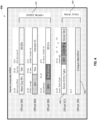
- FIG. 4 shows an example of a bit layout for a function association, in accordance with various embodiments.
- Figure 4 shows an example Function Association DVSEC 400, that includes a sequence of bits describing a DVSEC Header 402 with respective offsets, followed by one or more Associated Entry Fields 404. These fields are used to indicate which Application Function is associated with another Application Function.
- the Associated Entry Fields 404 include an associated entry type 406 and a unique identifier 408.
- Various Function Association types may include a trace aggregator association type that may be used with a Trace Hub Function, a telemetry association, or a timestamp association. Other future associations may be designed and added to the Function Association DVSEC 400.
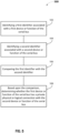
- FIG. 5 shows an example process for a computer system to identify a private or hidden connection between two devices or functions, in accordance with various embodiments.
- Process 500 may be implemented by CPU 102 and portions of system software 150 of FIG. 1 , and may interact with one or more elements as shown with respect to FIGs. 1 -4 to identify private or hidden connections between two devices or functions.
- the process includes identifying a first identifier associated with a first device or function of a serial bus.
- the first device or function may include Application Functions 110, 112, 120, 122, 126, 128, 132, 134 of FIG. 1 , with the first identifier available, respectively, in register 111, 113, 121, 123, 127, 129, 133, 135.
- the identifiers in the registers uniquely identify the respective Function Application and expose the identifier information to the CPU 102 and system software 150.
- the serial bus may be similar to PCIe buses 106, 116 of FIG. 1 .
- the first identifier may be similar to the unique identifier 408 of FIG. 4 .
- the process includes identifying a second identifier associated with a second device or function of the serial bus.
- the second device or function may include Application Functions 110, 112, 120, 122, 126, 128, 132, 134 of FIG. 1 , with the second identifier available, respectively, in register 111, 113, 121, 123, 127, 129, 133, 135.
- the identifiers in the registers uniquely identify the respective Function Application and expose the information to the CPU 102 and system software 150.
- the serial bus may be similar to PCIe buses 106, 116 of FIG. 1 .
- the first identifier may be similar to the unique identifier 408 of FIG. 4 .
- the process may include comparing the first identifier with the second identifier.
- the value of the first identifier is compared with the value the second identifier.
- determining whether the first device or function of the serial bus has a private physical or logical connection with the second device or function of the serial bus may be made if the value of the first identifier is equal to the value of the second identifier. In other embodiments, the determination may be made if there is a relationship between the value the first identifier and the value of the second identifier.
- an Association Entry Type such as Association Entry Type 406 of FIG. 4 may also be used to compare a type of the private physical or logical connection.
- all or part of the process 500 may be implemented during a PCIe enumeration performed by the operating system of CPU 102.
- the information on identifiers and types of the various devices or functions may be collected and published in a location within memory of the CPU 102.
- FIG. 6 illustrates an example computing device 600 suitable for use with various components of FIGs. 1-4 , in accordance with various embodiments.
- the computing device 600 may include the CPU 102 of FIG. 1 .
- computing device 600 may include one or more processors or processor cores 602 and system memory 604.
- processors or processor cores
- the processor 602 may include any type of processors, such as CPU 102, a microprocessor, and the like.
- the processor 602 may be implemented as an integrated circuit having multi-cores, e.g., a multi-core microprocessor.
- the computing device 600 may include mass storage devices 606 (such as diskette, hard drive, volatile memory (e.g., dynamic random-access memory (DRAM), compact disc read-only memory (CD-ROM), digital versatile disk (DVD), and so forth).
- volatile memory e.g., dynamic random-access memory (DRAM), compact disc read-only memory (CD-ROM), digital versatile disk (DVD), and so forth.
- system memory 604 and/or mass storage devices 606 may be temporal and/or persistent storage of any type, including, but not limited to, volatile and non-volatile memory, optical, magnetic, and/or solid state mass storage, and so forth.
- Volatile memory may include, but is not limited to, static and/or dynamic random access memory.
- Non-volatile memory may include, but is not limited to, electrically erasable programmable read-only memory, phase change memory, resistive memory, and so forth.
- the computing device 600 may further include I/O devices 608 (such as a display (e.g., a touchscreen display)), keyboard, cursor control, remote control, gaming controller, image capture device, a camera, one or more sensors, and so forth) and communication interfaces 510 (such as network interface cards, modems, infrared receivers, radio receivers (e.g., Bluetooth), and so forth).
- I/O devices 608 such as a display (e.g., a touchscreen display)
- keyboard cursor control, remote control, gaming controller, image capture device, a camera, one or more sensors, and so forth
- communication interfaces 510 such as network interface cards, modems, infrared receivers, radio receivers (e.g., Bluetooth), and so forth).
- the communication interfaces 610 may include communication chips (not shown) that may be configured to operate the device 600 in accordance with a Global System for Mobile Communication (GSM), General Packet Radio Service (GPRS), Universal Mobile Telecommunications System (UMTS), High Speed Packet Access (HSPA), Evolved HSPA (E-HSPA), or Long-Term Evolution (LTE) network.
- GSM Global System for Mobile Communication
- GPRS General Packet Radio Service
- UMTS Universal Mobile Telecommunications System
- High Speed Packet Access HSPA
- E-HSPA Evolved HSPA
- LTE Long-Term Evolution
- the communication chips may also be configured to operate in accordance with Enhanced Data for GSM Evolution (EDGE), GSM EDGE Radio Access Network (GERAN), Universal Terrestrial Radio Access Network (UTRAN), or Evolved UTRAN (E-UTRAN).
- EDGE Enhanced Data for GSM Evolution
- GERAN GSM EDGE Radio Access Network
- UTRAN Universal Terrestrial Radio Access Network
- the communication chips may be configured to operate in accordance with Code Division Multiple Access (CDMA), Time Division Multiple Access (TDMA), Digital Enhanced Cordless Telecommunications (DECT), Evolution-Data Optimized (EV-DO), derivatives thereof, as well as any other wireless protocols that are designated as 3G, 4G, 5G, and beyond.
- CDMA Code Division Multiple Access
- TDMA Time Division Multiple Access
- DECT Digital Enhanced Cordless Telecommunications
- EV-DO Evolution-Data Optimized
- derivatives thereof as well as any other wireless protocols that are designated as 3G, 4G, 5G, and beyond.
- system bus 612 may represent one or more buses, and which may include, for example, PCIe buses 106, 116.
- processors 602, memory 604, mass storage 606, communication interfaces 610 and I/o devices 608 may be PCIe devices.
- PCIe devices functions
- I/o devices 608 may be PCIe devices.
- they may be PCIe devices (functions) having private or hidden connections with other PCIe devices (functions), and incorporated with the teachings of the present disclosure to enable the private or hidden connections to be determined, as earlier described.
- multiple buses they may be bridged by one or more bus bridges (not shown).
- Each of these elements may perform its conventional functions known in the art.
- system memory 604 and mass storage devices 606 may be employed to store a working copy and a permanent copy of the programming instructions for the operation of various components of computing device 600, including but not limited to an operating system of computing device 600, one or more applications, and/or system software/firmware in support of practice of the present disclosure, such as OS 156, Trace Hub driver 154 and Debug Application 153 of Figure 1 , collectively referred to as computing logic 622, having private connection determination module 618.
- the various elements may be implemented by assembler instructions supported by processor(s) 602 or high-level languages that may be compiled into such instructions.
- the permanent copy of the programming instructions may be placed into mass storage devices 606 in the factory, or in the field through, for example, a distribution medium (not shown), such as a compact disc (CD), or through communication interface 610 (from a distribution server (not shown)). That is, one or more distribution media having an implementation of the agent program may be employed to distribute the agent and to program various computing devices.
- a distribution medium such as a compact disc (CD)
- CD compact disc
- communication interface 610 from a distribution server (not shown)
- the number, capability, and/or capacity of the elements 602, 604, 606, 608, 610, and 612 may vary, depending on whether computing device 600 is used as a stationary computing device, such as a set-top box or desktop computer, or a mobile computing device, such as a tablet computing device, laptop computer, game console, or smartphone. Their constitutions are otherwise known, and accordingly will not be further described.
- processors 602 may be packaged together with computational logic 622 configured to practice aspects of embodiments described herein to form a System in Package (SiP) or a System on Chip (SoC).
- SiP System in Package
- SoC System on Chip
- the computing device 600 may be one or more components of a data center, a laptop, a netbook, a notebook, an ultrabook, a smartphone, a tablet, a personal digital assistant (PDA), an ultra mobile PC, a mobile phone, a digital camera, or an IoT user equipment.
- the computing device 600 may be any other electronic device that processes data.
- FIG. 7 depicts a computer-readable storage medium that may be used in conjunction with the computing device 700, in accordance with various embodiments.
- Diagram 700 illustrates an example non-transitory computer-readable storage media 702 having instructions configured to practice all or selected ones of the operations associated with the processes described above.
- non-transitory computer-readable storage medium 702 may include a number of programming instructions 704 (e.g., including Private Connection Determination Module 618).
- Programming instructions 704 may be configured to enable a device, e.g., computing device 600, in response to execution of the programming instructions, to perform one or more operations of the processes described in reference to FIGs. 1-5 .
- programming instructions 704 may be disposed on multiple non-transitory computer-readable storage media 702 instead.
- programming instructions 704 may be encoded in transitory computer-readable signals.
- some embodiments may include one or more articles of manufacture (e.g., non-transitory computer-readable media) having instructions, stored thereon, that when executed result in actions of any of the above-described embodiments.
- some embodiments may include apparatuses or systems having any suitable means for carrying out the various operations of the above-described embodiments.
Landscapes
- Engineering & Computer Science (AREA)
- Theoretical Computer Science (AREA)
- General Engineering & Computer Science (AREA)
- Physics & Mathematics (AREA)
- General Physics & Mathematics (AREA)
- Software Systems (AREA)
- Computer Hardware Design (AREA)
- Quality & Reliability (AREA)
- Information Transfer Systems (AREA)
Claims (9)
- Computerimplementiertes Verfahren zum Bestimmen einer physischen oder logischen Verbindung zwischen Funktionen eines seriellen Busses (106, 116), wobei die Verbindung über verteilte Testfunktion DTF oder Intel On-Chip System Fabric Side Band IOSF-SB implementiert wird und vor Systemsoftware (150) einer CPU (102), die mit dem seriellen Bus (106, 116) verbunden ist, verborgen ist, wobei das Verfahren Folgendes umfasst:Identifizieren einer mit einer ersten Funktion des seriellen Busses (106, 116) assoziierten ersten Kennung durch eine Datenverarbeitungssvorrichtung;Identifizieren einer mit einer zweiten Funktion des seriellen Busses (106, 116) assoziierten zweiten Kennung durch die Datenverarbeitungsvorrichtung;Vergleichen der ersten Kennung mit der zweiten Kennung durch die Datenverarbeitungsvorrichtung, wobei Vergleichen der ersten Kennung mit der zweiten Kennung ferner Vergleichen eines ersten Assoziationstyps mit einem zweiten Assoziationstyp umfasst, wobei der erste und zweite Assoziationstyp einen jeweiligen Typ der entsprechenden Funktion angeben; undBestimmen durch die Datenverarbeitungsvorrichtung auf der Basis des Vergleichs, ob die erste Funktion des seriellen Busses (106, 116) eine physische oder logische Verbindung mit der zweiten Funktion des seriellen Busses (106, 116) aufweist, wobei die Verbindung über DTF oder IOSF-SB implementiert wird und vor der Systemsoftware (150) verborgen ist.
- Computerimplementiertes Verfahren nach Anspruch 1, wobei der serielle Bus (106, 116) ein PCIe-Bus ist.
- Computerimplementiertes Verfahren nach Anspruch 1, wobei die zweite Funktion des seriellen Busses (106, 116) eine Vielzahl von Funktionen ist.
- Computerimplementiertes Verfahren nach einem der Ansprüche 1-3, wobei die erste Kennung in einem Register der designierten vertreiberspezifischen erweiterten Fähigkeitsstruktur DVSEC der ersten Funktion gespeichert wird und die zweite Kennung in einem Register der DVSEC der zweiten Funktion gespeichert wird.
- Computerimplementiertes Verfahren nach einem der Ansprüche 1-3, wobei es sich bei der ersten Kennung und der zweiten Kennung um eine vorbestimmte feste Kennung handelt.
- Verfahren nach Anspruch 1, wobei die Kennungen für ein System einzigartig sind, global einzigartige Kennungen GUID sind oder universell einzigartige Kennungen UUID sind.
- Verfahren nach Anspruch 1, wobei die Kennungen gleich sind.
- Verfahren nach einem der Ansprüche 1-7, wobei die erste und zweite Funktion PCIe-Funktionen sind.
- Datenverarbeitungssvorrichtung zum Bestimmen einer physischen oder logischen Verbindung zwischen Vorrichtungen oder Funktionen eines seriellen Busses (106, 116), wobei die Verbindung über verteilte Testfunktion DTF oder Intel On-Chips System Fabric Side Band IOSF-SB implementiert wird und vor Systemsoftware (150) einer CPU (102), die mit dem seriellen Bus (106, 116) verbunden ist, verborgen ist, wobei die Datenverarbeitungsvorrichtung Folgendes umfasst:Mittel zum Identifizieren einer mit einer ersten Funktion des seriellen Busses assoziierten ersten Kennung;Mittel zum Identifizieren einer mit einer zweiten Funktion des seriellen Busses assoziierten zweiten Kennung;Mittel zum Vergleichen der ersten Kennung mit der zweiten Kennung durch die Datenverarbeitungsvorrichtung, wobei Vergleichen der ersten Kennung mit der zweiten Kennung ferner Vergleichen eines ersten Assoziationstyps mit einem zweiten Assoziationstyp umfasst, wobei der erste und zweite Assoziationstyp einen jeweiligen Typ der entsprechenden Funktion angeben; undMittel zum Bestimmen auf der Basis des Vergleichs, ob die erste Funktion des seriellen Busses (106, 116) eine physische oder logische Verbindung mit der zweiten Funktion des seriellen Busses (106, 116) aufweist, wobei die Verbindung über DTF oder IOSF-SB implementiert wird und vor der Systemsoftware (150) verborgen ist.
Applications Claiming Priority (1)
| Application Number | Priority Date | Filing Date | Title |
|---|---|---|---|
| US16/931,073 US11995018B2 (en) | 2020-07-16 | 2020-07-16 | Determining a private connection between devices or functions of a serial bus |
Publications (2)
| Publication Number | Publication Date |
|---|---|
| EP3940545A1 EP3940545A1 (de) | 2022-01-19 |
| EP3940545B1 true EP3940545B1 (de) | 2023-11-29 |
Family
ID=73017716
Family Applications (1)
| Application Number | Title | Priority Date | Filing Date |
|---|---|---|---|
| EP20208325.9A Active EP3940545B1 (de) | 2020-07-16 | 2020-11-18 | Bestimmung einer privaten verbindung zwischen geräten oder funktionen eines seriellen busses |
Country Status (3)
| Country | Link |
|---|---|
| US (1) | US11995018B2 (de) |
| EP (1) | EP3940545B1 (de) |
| CN (1) | CN113946531A (de) |
Family Cites Families (4)
| Publication number | Priority date | Publication date | Assignee | Title |
|---|---|---|---|---|
| US8713234B2 (en) * | 2011-09-29 | 2014-04-29 | Intel Corporation | Supporting multiple channels of a single interface |
| US10545773B2 (en) | 2018-05-23 | 2020-01-28 | Intel Corporation | System, method, and apparatus for DVSEC for efficient peripheral management |
| US10521388B2 (en) * | 2018-09-28 | 2019-12-31 | Intel Corporation | Multi-uplink device enumeration and management |
| US10901871B2 (en) * | 2019-03-05 | 2021-01-26 | Intel Corporation | System, apparatus and method for dynamic multi-source tracing in a system |
-
2020
- 2020-07-16 US US16/931,073 patent/US11995018B2/en active Active
- 2020-11-18 EP EP20208325.9A patent/EP3940545B1/de active Active
- 2020-12-23 CN CN202011572693.3A patent/CN113946531A/zh active Pending
Also Published As
| Publication number | Publication date |
|---|---|
| EP3940545A1 (de) | 2022-01-19 |
| US11995018B2 (en) | 2024-05-28 |
| CN113946531A (zh) | 2022-01-18 |
| US20200349101A1 (en) | 2020-11-05 |
Similar Documents
| Publication | Publication Date | Title |
|---|---|---|
| CN106970864B (zh) | 片上系统、移动终端和用于操作片上系统的方法 | |
| US9612887B2 (en) | Firmware-related event notification | |
| KR101679947B1 (ko) | 입력/출력 에러-억제 이벤트 후의 복구 | |
| US6378064B1 (en) | Microcomputer | |
| CN113806006A (zh) | 一种异构指令集架构下异常或中断的处理方法、装置 | |
| US20040003324A1 (en) | Handling faults associated with operation of guest software in the virtual-machine architecture | |
| US20040003323A1 (en) | Control over faults occurring during the operation of guest software in the virtual-machine architecture | |
| US11163659B2 (en) | Enhanced serial peripheral interface (eSPI) signaling for crash event notification | |
| KR20110083518A (ko) | 호스트 usb 어댑터 가상화 | |
| EP2941694B1 (de) | Fähigkeitsbasiertes gerätetreiberframework | |
| EP2941696A1 (de) | Softwareschnittstelle für eine hardwarevorrichtung | |
| CN114398172A (zh) | 资源配置方法、装置、电子设备及计算机可读存储介质 | |
| CN106909835B (zh) | 一种基于cpu时空隔离机制实现内核完整性度量的方法 | |
| US9372702B2 (en) | Non-disruptive code update of a single processor in a multi-processor computing system | |
| US20170249457A1 (en) | Secure receive packet processing for network function virtualization applications | |
| US20190050350A1 (en) | USB Method and Apparatus in a Virtualization Environment with Multi-VM | |
| US10496573B2 (en) | Context-sensitive interrupts | |
| CN114329439B (zh) | 片上系统和中断隔离方法及计算机设备 | |
| CN119065886B (zh) | Io设备的错误处理方法、宿主机、设备、介质和产品 | |
| US11995018B2 (en) | Determining a private connection between devices or functions of a serial bus | |
| EP2941695B1 (de) | In einen verwalteten code implementierte benutzermodustreiber mit hohem durchsatz und niedriger latenz | |
| CN107025196B (zh) | 物理层设备操作系统以及方法 | |
| KR20190138031A (ko) | 반도체 장치 |
Legal Events
| Date | Code | Title | Description |
|---|---|---|---|
| PUAI | Public reference made under article 153(3) epc to a published international application that has entered the european phase |
Free format text: ORIGINAL CODE: 0009012 |
|
| STAA | Information on the status of an ep patent application or granted ep patent |
Free format text: STATUS: THE APPLICATION HAS BEEN PUBLISHED |
|
| AK | Designated contracting states |
Kind code of ref document: A1 Designated state(s): AL AT BE BG CH CY CZ DE DK EE ES FI FR GB GR HR HU IE IS IT LI LT LU LV MC MK MT NL NO PL PT RO RS SE SI SK SM TR |
|
| STAA | Information on the status of an ep patent application or granted ep patent |
Free format text: STATUS: REQUEST FOR EXAMINATION WAS MADE |
|
| 17P | Request for examination filed |
Effective date: 20220714 |
|
| RBV | Designated contracting states (corrected) |
Designated state(s): AL AT BE BG CH CY CZ DE DK EE ES FI FR GB GR HR HU IE IS IT LI LT LU LV MC MK MT NL NO PL PT RO RS SE SI SK SM TR |
|
| GRAP | Despatch of communication of intention to grant a patent |
Free format text: ORIGINAL CODE: EPIDOSNIGR1 |
|
| STAA | Information on the status of an ep patent application or granted ep patent |
Free format text: STATUS: GRANT OF PATENT IS INTENDED |
|
| INTG | Intention to grant announced |
Effective date: 20230621 |
|
| GRAS | Grant fee paid |
Free format text: ORIGINAL CODE: EPIDOSNIGR3 |
|
| GRAA | (expected) grant |
Free format text: ORIGINAL CODE: 0009210 |
|
| STAA | Information on the status of an ep patent application or granted ep patent |
Free format text: STATUS: THE PATENT HAS BEEN GRANTED |
|
| AK | Designated contracting states |
Kind code of ref document: B1 Designated state(s): AL AT BE BG CH CY CZ DE DK EE ES FI FR GB GR HR HU IE IS IT LI LT LU LV MC MK MT NL NO PL PT RO RS SE SI SK SM TR |
|
| REG | Reference to a national code |
Ref country code: GB Ref legal event code: FG4D |
|
| REG | Reference to a national code |
Ref country code: CH Ref legal event code: EP |
|
| REG | Reference to a national code |
Ref country code: DE Ref legal event code: R096 Ref document number: 602020021813 Country of ref document: DE |
|
| REG | Reference to a national code |
Ref country code: IE Ref legal event code: FG4D |
|
| P01 | Opt-out of the competence of the unified patent court (upc) registered |
Effective date: 20231120 |
|
| REG | Reference to a national code |
Ref country code: NL Ref legal event code: FP |
|
| REG | Reference to a national code |
Ref country code: LT Ref legal event code: MG9D |
|
| PG25 | Lapsed in a contracting state [announced via postgrant information from national office to epo] |
Ref country code: GR Free format text: LAPSE BECAUSE OF FAILURE TO SUBMIT A TRANSLATION OF THE DESCRIPTION OR TO PAY THE FEE WITHIN THE PRESCRIBED TIME-LIMIT Effective date: 20240301 |
|
| PG25 | Lapsed in a contracting state [announced via postgrant information from national office to epo] |
Ref country code: IS Free format text: LAPSE BECAUSE OF FAILURE TO SUBMIT A TRANSLATION OF THE DESCRIPTION OR TO PAY THE FEE WITHIN THE PRESCRIBED TIME-LIMIT Effective date: 20240329 |
|
| PG25 | Lapsed in a contracting state [announced via postgrant information from national office to epo] |
Ref country code: LT Free format text: LAPSE BECAUSE OF FAILURE TO SUBMIT A TRANSLATION OF THE DESCRIPTION OR TO PAY THE FEE WITHIN THE PRESCRIBED TIME-LIMIT Effective date: 20231129 |
|
| PG25 | Lapsed in a contracting state [announced via postgrant information from national office to epo] |
Ref country code: ES Free format text: LAPSE BECAUSE OF FAILURE TO SUBMIT A TRANSLATION OF THE DESCRIPTION OR TO PAY THE FEE WITHIN THE PRESCRIBED TIME-LIMIT Effective date: 20231129 |
|
| PG25 | Lapsed in a contracting state [announced via postgrant information from national office to epo] |
Ref country code: LT Free format text: LAPSE BECAUSE OF FAILURE TO SUBMIT A TRANSLATION OF THE DESCRIPTION OR TO PAY THE FEE WITHIN THE PRESCRIBED TIME-LIMIT Effective date: 20231129 Ref country code: IS Free format text: LAPSE BECAUSE OF FAILURE TO SUBMIT A TRANSLATION OF THE DESCRIPTION OR TO PAY THE FEE WITHIN THE PRESCRIBED TIME-LIMIT Effective date: 20240329 Ref country code: GR Free format text: LAPSE BECAUSE OF FAILURE TO SUBMIT A TRANSLATION OF THE DESCRIPTION OR TO PAY THE FEE WITHIN THE PRESCRIBED TIME-LIMIT Effective date: 20240301 Ref country code: ES Free format text: LAPSE BECAUSE OF FAILURE TO SUBMIT A TRANSLATION OF THE DESCRIPTION OR TO PAY THE FEE WITHIN THE PRESCRIBED TIME-LIMIT Effective date: 20231129 Ref country code: BG Free format text: LAPSE BECAUSE OF FAILURE TO SUBMIT A TRANSLATION OF THE DESCRIPTION OR TO PAY THE FEE WITHIN THE PRESCRIBED TIME-LIMIT Effective date: 20240229 |
|
| REG | Reference to a national code |
Ref country code: AT Ref legal event code: MK05 Ref document number: 1636841 Country of ref document: AT Kind code of ref document: T Effective date: 20231129 |
|
| PG25 | Lapsed in a contracting state [announced via postgrant information from national office to epo] |
Ref country code: SE Free format text: LAPSE BECAUSE OF FAILURE TO SUBMIT A TRANSLATION OF THE DESCRIPTION OR TO PAY THE FEE WITHIN THE PRESCRIBED TIME-LIMIT Effective date: 20231129 Ref country code: RS Free format text: LAPSE BECAUSE OF FAILURE TO SUBMIT A TRANSLATION OF THE DESCRIPTION OR TO PAY THE FEE WITHIN THE PRESCRIBED TIME-LIMIT Effective date: 20231129 Ref country code: PL Free format text: LAPSE BECAUSE OF FAILURE TO SUBMIT A TRANSLATION OF THE DESCRIPTION OR TO PAY THE FEE WITHIN THE PRESCRIBED TIME-LIMIT Effective date: 20231129 Ref country code: NO Free format text: LAPSE BECAUSE OF FAILURE TO SUBMIT A TRANSLATION OF THE DESCRIPTION OR TO PAY THE FEE WITHIN THE PRESCRIBED TIME-LIMIT Effective date: 20240229 Ref country code: LV Free format text: LAPSE BECAUSE OF FAILURE TO SUBMIT A TRANSLATION OF THE DESCRIPTION OR TO PAY THE FEE WITHIN THE PRESCRIBED TIME-LIMIT Effective date: 20231129 Ref country code: HR Free format text: LAPSE BECAUSE OF FAILURE TO SUBMIT A TRANSLATION OF THE DESCRIPTION OR TO PAY THE FEE WITHIN THE PRESCRIBED TIME-LIMIT Effective date: 20231129 |
|
| PG25 | Lapsed in a contracting state [announced via postgrant information from national office to epo] |
Ref country code: DK Free format text: LAPSE BECAUSE OF FAILURE TO SUBMIT A TRANSLATION OF THE DESCRIPTION OR TO PAY THE FEE WITHIN THE PRESCRIBED TIME-LIMIT Effective date: 20231129 |
|
| PG25 | Lapsed in a contracting state [announced via postgrant information from national office to epo] |
Ref country code: CZ Free format text: LAPSE BECAUSE OF FAILURE TO SUBMIT A TRANSLATION OF THE DESCRIPTION OR TO PAY THE FEE WITHIN THE PRESCRIBED TIME-LIMIT Effective date: 20231129 Ref country code: AT Free format text: LAPSE BECAUSE OF FAILURE TO SUBMIT A TRANSLATION OF THE DESCRIPTION OR TO PAY THE FEE WITHIN THE PRESCRIBED TIME-LIMIT Effective date: 20231129 |
|
| PG25 | Lapsed in a contracting state [announced via postgrant information from national office to epo] |
Ref country code: SK Free format text: LAPSE BECAUSE OF FAILURE TO SUBMIT A TRANSLATION OF THE DESCRIPTION OR TO PAY THE FEE WITHIN THE PRESCRIBED TIME-LIMIT Effective date: 20231129 |
|
| PG25 | Lapsed in a contracting state [announced via postgrant information from national office to epo] |
Ref country code: SM Free format text: LAPSE BECAUSE OF FAILURE TO SUBMIT A TRANSLATION OF THE DESCRIPTION OR TO PAY THE FEE WITHIN THE PRESCRIBED TIME-LIMIT Effective date: 20231129 Ref country code: SK Free format text: LAPSE BECAUSE OF FAILURE TO SUBMIT A TRANSLATION OF THE DESCRIPTION OR TO PAY THE FEE WITHIN THE PRESCRIBED TIME-LIMIT Effective date: 20231129 Ref country code: RO Free format text: LAPSE BECAUSE OF FAILURE TO SUBMIT A TRANSLATION OF THE DESCRIPTION OR TO PAY THE FEE WITHIN THE PRESCRIBED TIME-LIMIT Effective date: 20231129 Ref country code: IT Free format text: LAPSE BECAUSE OF FAILURE TO SUBMIT A TRANSLATION OF THE DESCRIPTION OR TO PAY THE FEE WITHIN THE PRESCRIBED TIME-LIMIT Effective date: 20231129 Ref country code: EE Free format text: LAPSE BECAUSE OF FAILURE TO SUBMIT A TRANSLATION OF THE DESCRIPTION OR TO PAY THE FEE WITHIN THE PRESCRIBED TIME-LIMIT Effective date: 20231129 Ref country code: DK Free format text: LAPSE BECAUSE OF FAILURE TO SUBMIT A TRANSLATION OF THE DESCRIPTION OR TO PAY THE FEE WITHIN THE PRESCRIBED TIME-LIMIT Effective date: 20231129 Ref country code: CZ Free format text: LAPSE BECAUSE OF FAILURE TO SUBMIT A TRANSLATION OF THE DESCRIPTION OR TO PAY THE FEE WITHIN THE PRESCRIBED TIME-LIMIT Effective date: 20231129 Ref country code: AT Free format text: LAPSE BECAUSE OF FAILURE TO SUBMIT A TRANSLATION OF THE DESCRIPTION OR TO PAY THE FEE WITHIN THE PRESCRIBED TIME-LIMIT Effective date: 20231129 |
|
| PG25 | Lapsed in a contracting state [announced via postgrant information from national office to epo] |
Ref country code: PT Free format text: LAPSE BECAUSE OF FAILURE TO SUBMIT A TRANSLATION OF THE DESCRIPTION OR TO PAY THE FEE WITHIN THE PRESCRIBED TIME-LIMIT Effective date: 20240401 |
|
| PG25 | Lapsed in a contracting state [announced via postgrant information from national office to epo] |
Ref country code: PT Free format text: LAPSE BECAUSE OF FAILURE TO SUBMIT A TRANSLATION OF THE DESCRIPTION OR TO PAY THE FEE WITHIN THE PRESCRIBED TIME-LIMIT Effective date: 20240401 |
|
| REG | Reference to a national code |
Ref country code: DE Ref legal event code: R097 Ref document number: 602020021813 Country of ref document: DE |
|
| PLBE | No opposition filed within time limit |
Free format text: ORIGINAL CODE: 0009261 |
|
| STAA | Information on the status of an ep patent application or granted ep patent |
Free format text: STATUS: NO OPPOSITION FILED WITHIN TIME LIMIT |
|
| PG25 | Lapsed in a contracting state [announced via postgrant information from national office to epo] |
Ref country code: SI Free format text: LAPSE BECAUSE OF FAILURE TO SUBMIT A TRANSLATION OF THE DESCRIPTION OR TO PAY THE FEE WITHIN THE PRESCRIBED TIME-LIMIT Effective date: 20231129 |
|
| PG25 | Lapsed in a contracting state [announced via postgrant information from national office to epo] |
Ref country code: SI Free format text: LAPSE BECAUSE OF FAILURE TO SUBMIT A TRANSLATION OF THE DESCRIPTION OR TO PAY THE FEE WITHIN THE PRESCRIBED TIME-LIMIT Effective date: 20231129 |
|
| 26N | No opposition filed |
Effective date: 20240830 |
|
| REG | Reference to a national code |
Ref country code: CH Ref legal event code: PL |
|
| PG25 | Lapsed in a contracting state [announced via postgrant information from national office to epo] |
Ref country code: MC Free format text: LAPSE BECAUSE OF FAILURE TO SUBMIT A TRANSLATION OF THE DESCRIPTION OR TO PAY THE FEE WITHIN THE PRESCRIBED TIME-LIMIT Effective date: 20231129 |
|
| PG25 | Lapsed in a contracting state [announced via postgrant information from national office to epo] |
Ref country code: LU Free format text: LAPSE BECAUSE OF NON-PAYMENT OF DUE FEES Effective date: 20241118 |
|
| REG | Reference to a national code |
Ref country code: CH Ref legal event code: PL |
|
| PG25 | Lapsed in a contracting state [announced via postgrant information from national office to epo] |
Ref country code: CH Free format text: LAPSE BECAUSE OF NON-PAYMENT OF DUE FEES Effective date: 20241130 |
|
| REG | Reference to a national code |
Ref country code: BE Ref legal event code: MM Effective date: 20241130 |
|
| PG25 | Lapsed in a contracting state [announced via postgrant information from national office to epo] |
Ref country code: FI Free format text: LAPSE BECAUSE OF FAILURE TO SUBMIT A TRANSLATION OF THE DESCRIPTION OR TO PAY THE FEE WITHIN THE PRESCRIBED TIME-LIMIT Effective date: 20231129 |
|
| PG25 | Lapsed in a contracting state [announced via postgrant information from national office to epo] |
Ref country code: BE Free format text: LAPSE BECAUSE OF NON-PAYMENT OF DUE FEES Effective date: 20241130 |
|
| PG25 | Lapsed in a contracting state [announced via postgrant information from national office to epo] |
Ref country code: IE Free format text: LAPSE BECAUSE OF NON-PAYMENT OF DUE FEES Effective date: 20241118 |
|
| PGFP | Annual fee paid to national office [announced via postgrant information from national office to epo] |
Ref country code: NL Payment date: 20251024 Year of fee payment: 6 |
|
| PGFP | Annual fee paid to national office [announced via postgrant information from national office to epo] |
Ref country code: DE Payment date: 20250923 Year of fee payment: 6 |
|
| PGFP | Annual fee paid to national office [announced via postgrant information from national office to epo] |
Ref country code: GB Payment date: 20251016 Year of fee payment: 6 |
|
| PGFP | Annual fee paid to national office [announced via postgrant information from national office to epo] |
Ref country code: FR Payment date: 20251023 Year of fee payment: 6 |
|
| PG25 | Lapsed in a contracting state [announced via postgrant information from national office to epo] |
Ref country code: HU Free format text: LAPSE BECAUSE OF FAILURE TO SUBMIT A TRANSLATION OF THE DESCRIPTION OR TO PAY THE FEE WITHIN THE PRESCRIBED TIME-LIMIT; INVALID AB INITIO Effective date: 20201118 |
|
| PG25 | Lapsed in a contracting state [announced via postgrant information from national office to epo] |
Ref country code: CY Free format text: LAPSE BECAUSE OF FAILURE TO SUBMIT A TRANSLATION OF THE DESCRIPTION OR TO PAY THE FEE WITHIN THE PRESCRIBED TIME-LIMIT; INVALID AB INITIO Effective date: 20201118 |