EP3940513A1 - Touch panel - Google Patents
Touch panel Download PDFInfo
- Publication number
- EP3940513A1 EP3940513A1 EP20813978.2A EP20813978A EP3940513A1 EP 3940513 A1 EP3940513 A1 EP 3940513A1 EP 20813978 A EP20813978 A EP 20813978A EP 3940513 A1 EP3940513 A1 EP 3940513A1
- Authority
- EP
- European Patent Office
- Prior art keywords
- area
- electrode
- predetermined direction
- facing portion
- touch panel
- Prior art date
- Legal status (The legal status is an assumption and is not a legal conclusion. Google has not performed a legal analysis and makes no representation as to the accuracy of the status listed.)
- Withdrawn
Links
Images







Classifications
-
- G—PHYSICS
- G06—COMPUTING OR CALCULATING; COUNTING
- G06F—ELECTRIC DIGITAL DATA PROCESSING
- G06F3/00—Input arrangements for transferring data to be processed into a form capable of being handled by the computer; Output arrangements for transferring data from processing unit to output unit, e.g. interface arrangements
- G06F3/01—Input arrangements or combined input and output arrangements for interaction between user and computer
- G06F3/03—Arrangements for converting the position or the displacement of a member into a coded form
- G06F3/041—Digitisers, e.g. for touch screens or touch pads, characterised by the transducing means
- G06F3/044—Digitisers, e.g. for touch screens or touch pads, characterised by the transducing means by capacitive means
- G06F3/0443—Digitisers, e.g. for touch screens or touch pads, characterised by the transducing means by capacitive means using a single layer of sensing electrodes
-
- G—PHYSICS
- G06—COMPUTING OR CALCULATING; COUNTING
- G06F—ELECTRIC DIGITAL DATA PROCESSING
- G06F3/00—Input arrangements for transferring data to be processed into a form capable of being handled by the computer; Output arrangements for transferring data from processing unit to output unit, e.g. interface arrangements
- G06F3/01—Input arrangements or combined input and output arrangements for interaction between user and computer
- G06F3/03—Arrangements for converting the position or the displacement of a member into a coded form
- G06F3/041—Digitisers, e.g. for touch screens or touch pads, characterised by the transducing means
- G06F3/044—Digitisers, e.g. for touch screens or touch pads, characterised by the transducing means by capacitive means
- G06F3/0448—Details of the electrode shape, e.g. for enhancing the detection of touches, for generating specific electric field shapes, for enhancing display quality
-
- G—PHYSICS
- G06—COMPUTING OR CALCULATING; COUNTING
- G06F—ELECTRIC DIGITAL DATA PROCESSING
- G06F2203/00—Indexing scheme relating to G06F3/00 - G06F3/048
- G06F2203/041—Indexing scheme relating to G06F3/041 - G06F3/045
- G06F2203/04112—Electrode mesh in capacitive digitiser: electrode for touch sensing is formed of a mesh of very fine, normally metallic, interconnected lines that are almost invisible to see. This provides a quite large but transparent electrode surface, without need for ITO or similar transparent conductive material
Definitions
- This invention relates to a touch panel, in particular, to a mutual capacitive system touch panel.
- Patent Document 1 discloses an example of a mutual capacitive system touch panel (hereinafter referred to as a touch panel).
- the touch panel of Patent Document 1 has a plurality of sensor portions, and each of the sensor portions is provided with an electrode layer formed on a base member.
- the electrode layer disclosed in Patent Document 1 has a first electrode 91, a second electrode 93 and a dummy electrode 95.
- Each of the first electrode 91 and the second electrode 93 is formed to have a comb teeth-like shape.
- Comb teeth (first line-like parts) 911 of the first electrode 91 and comb teeth (second line-like parts) 931 of the second electrode extend in a perpendicular direction perpendicular to a predetermined direction.
- the first line-like parts 911 and the second line-like parts 931 are alternately arranged in the predetermined direction.
- the dummy electrode 95 is arranged between the first electrode 91 and the second electrode 93.
- the first electrode 91 and the second electrode 93 form a capacitor.
- a conductor such as a finger
- capacitance of the capacitor is varied.
- the touch panel of Patent Document 1 can detect approach of the conductor to the sensor portion.
- Patent Document 1 JP2018-112842A
- Patent Document 1 discloses that sensitivity of the sensor portion can be increased by widening intervals between the first line-shape parts 911 and the second line-shape parts 931 in the predetermined direction.
- widening the intervals between the first line-like parts 911 and the second line-like parts 931 in the touch panel or the sensor portion causes expansion of a size of the touch panel or the sensor portion.
- resolution of the touch panel or the sensor portion is reduced. Accordingly, there is a demand to provide a touch panel which can improve sensitivity of a touch panel or a sensor portion thereof without reducing resolution of the touch panel or the sensor portion.
- One aspect of the present invention provides a touch panel comprising a base member and an electrode layer formed on the base member, wherein:
- Resolution of the touch panel of the present invention depends on an interval between the first area and the second area.
- sensitivity of the touch panel of the present invention depends on a width of the intervening portion in the predetermined direction. As apparent from what the first end region and the second end region overlap with the first region and the second region, respectively, the width of the intervening portion is wider than the interval between the first region and the second region. Accordingly, the touch panel of the present invention can achieve higher detection sensitivity in comparison with a touch panel in which a first end region of an intervening portion and a second end region of the intervening portion do not overlap with a first region and a second region, respectively. Thus, the touch panel of the present invention can improve the detection sensitivity without reducing the resolution.
- a mutual capacitive system touch panel (a touch panel) 10 is provided with a base member 12, an electrode layer 14 formed on a surface of the base member 12 and a protective layer 16 provided on the surface of the base member 12 to cover the electrode layer 14.
- the base member 12 may be a plate-like or film-like member which is made of glass or resin to be optically transparent.
- the electrode layer 14 consists of a conductive mesh 30 (see Fig. 3 ) formed on the surface of the base member 12.
- the conductive mesh 30 may be formed on the surface of the base member 12 by printing using conductive ink or by etching a conductive layer formed on the surface of the base member 12 by vacuum deposition.
- the protective layer 16 may be formed by spin coating or printing using ink-like resin. Alternatively, the protective layer 16 may be formed by sticking a cover member made of glass or resin with adhesive.
- the electrode layer 14 is provided with a plurality of first electrodes 21, a plurality of second electrodes 23, a plurality of dummy electrodes 25 and a plurality of wirings 27.
- an area where each of the first electrodes 21 and the second electrodes 23 overlaps with an area where any one of the dummy electrodes 25 is formed (a dummy area 45: see Fig. 3 ).
- a dummy area 45 see Fig. 3
- Fig. 2 in order to show schematic arrangement of the first electrodes 21, the second electrodes 23 and the dummy electrodes 25, there is a space between each of the first electrodes 21 and the second electrodes 23 and any one of the dummy electrodes 25.
- the first electrodes 21 are five in number, and the second electrodes 23 are twenty in number. Moreover, in the present embodiment, each of the first electrodes 21 is combined with four of the second electrodes 23.
- the wirings 27 are connected to the first electrodes 21 and the second electrodes 23, respectively.
- the number of the first electrodes 21 and the number of the second electrodes 23 may be freely set.
- the ratio of the number of the first electrodes 21 to the number of the second electrodes 23 may be freely set, where the first electrodes 21 and the second electrodes 23 are combined with each other. For example, the first electrodes 21 and the second electrodes 23 may be combined with each other one to one.
- each of the first electrodes 21 and the second electrodes 23 is formed to have comb teeth-like shape.
- each of the first electrodes 21 has a first main portion 211 extending along a predetermined direction and a plurality of first facing portions 213 extending from the first main portion 211 along a perpendicular direction perpendicular to the predetermined direction.
- each of the second electrodes 23 has a second main portion 231 extending along the predetermined direction and a plurality of second facing portions 233 extending from the second main portion 231 along the perpendicular direction.
- the predetermined direction is a Y-direction
- the perpendicular direction is an X-direction.
- the first facing portions 213 extend from the first main portion 211 in a positive X-direction
- the second facing portions 233 extend from the second main portion 231 in a negative X-direction.
- the first facing portions 213 and the second facing portions 233 are alternately arranged in the predetermined direction.
- the first facing portion 213 and the second facing portion 233 which are adjacent to each other are apart from each other and face each other.
- the first electrode 21 and each of the second electrodes 23 form a capacitor.
- the electrode layer 14 consists of the conductive mesh 30.
- the conductive mesh 30 has a pattern in which specific elements 31 are repeatedly arranged in two dimensions.
- the specific element 31 has a diamond shape.
- the specific element 31 is arranged so that two diagonal lines thereof are parallel to the predetermined direction and the perpendicular direction, respectively.
- the present invention is not limited thereto.
- the specific element 31 may have a shape other than the diamond shape.
- the conductive mesh 30 has discontinuities between the first electrode 21 and the dummy electrode 25 and between the dummy electrode 25 and the second electrode 23.
- the conductive mesh 30 is divided between the first electrode 21 and the dummy electrode 25 and between the dummy electrode 25 and the second electrode 23.
- the division of the conductive mesh 30 is made so that an imaginary line cannot drawn each of between the first electrode 21 and the dummy electrode 25 and between the dummy electrode 25 and the second electrode 23.
- the first facing portion 213 of the first electrode 21 and the second facing portion 233 of the second electrode 23 which are adjacent to each other are apart from each other and face each other.
- an intervening portion 251 of the dummy electrode 25 intervenes.
- the dummy electrode 25 has the intervening portion 251 which is located between the first facing portion 213 and the second facing portion 233 at least in part.
- the first facing portion 213 of the first electrode 21 is formed in the first area 41.
- the first area 41 is an area defined by imaginarily linking outermost ends 321 of a part of the conductive mesh 30 that forms the first facing portion 213.
- the second facing portion 233 of the second electrode 23 is formed in the second area 43.
- the second area 43 is an area defined by imaginarily linking outermost ends 323 of a part of the conductive mesh 30 that forms the second facing portion 233.
- the conductive mesh 30 has the pattern in which the specific elements 31 are repeatedly arranged in the perpendicular direction.
- the specific element 31 has a predetermined size as a maximum size in perpendicular direction.
- the predetermined size is equal to a length of the diagonal line of the specific element 31 in the perpendicular direction.
- the first area 41 is formed by imaginarily linking the outermost ends 321 of the area of the conductive mesh 30 that forms the first facing portion 213, wherein the outermost ends 321 are arranged at intervals of the predetermined size in the perpendicular direction.
- the line linking the outermost ends 321 form an edge along the perpendicular direction.
- the first area 41 has, as an end edge in the predetermined direction, an edge straightly extending in the perpendicular direction.
- the second area 43 is formed by imaginarily linking the outermost ends 323 of the part of the conductive mesh 30 that forms the second facing portion 233, wherein the outermost ends 323 are arranged at intervals of the predetermined size in the perpendicular direction.
- the line linking the outermost ends 323 form an edge along the perpendicular direction.
- the second area 43 has, as an end edge in the predetermined direction, an edge straightly extending in the perpendicular direction.
- the intervening portion 251 of the dummy electrode 25 is formed in the dummy area 45.
- the dummy area 45 is an area defined by imaginarily linking outermost ends 325 and 357 of a part of the conductive mesh 30 that forms the intervening portion 251.
- the dummy area 45 has a first end area 451 and a second end area 453 as both end areas thereof in the predetermined direction.
- the first end area 451 is an area overlapping with the first area 41
- the second end area 453 is an area overlapping with the second area 43.
- the intervening portion 251 has a plurality of first specific lines 331 parallel to one another in the first end area 451.
- Each of the first specific lines 331 corresponds to an edge of the diamond shape of the specific element 31.
- each of the first specific lines 331 corresponds to a part of the edge of the diamond shape of the specific element 31.
- the first facing portion 213 has a plurality of first end lines 341 parallel to one another as an end portion thereof in the predetermined direction.
- Each of the first end lines 341 corresponds to an edge of the diamond shape of the specific element 31.
- each of the first specific lines 331 corresponds to a part of the edge of the diamond shape of the specific element 31.
- the first specific lines 331 and the first end lines 341 are alternately arranged in the perpendicular direction.
- the intervening portion 251 further has a plurality of second specific lines 333 parallel to one another in the second end area 453.
- Each of the second specific lines 333 corresponds to an edge of the diamond shape of the specific element 31.
- each of the second specific lines 333 corresponds to a part of the edge of the diamond shape of the specific element 31.
- the second facing portion 233 has a plurality of second end lines 343 parallel to one another as an end portion thereof in the predetermined direction.
- Each of the second end lines 343 corresponds to an edge of the diamond shape of the specific element 31.
- each of the second specific lines 333 corresponds to a part of the edge of the diamond shape of the specific element 31.
- the second specific lines 333 and the second end lines 343 are alternately arranged in the perpendicular direction.
- the intervening portion 251 of the dummy electrode 25 enters each of the first area 41 and the second area 43 in part in the predetermined direction.
- resolution of the touch panel 10 mainly depends on a shortest distance between the first electrode 21 and the second electrode 23 in the predetermined direction or a distance between the first area 41 and the second area 43 in the predetermined direction.
- sensitivity of the touch panel 10 mainly depends on a maximum width of the intervening portion 251 of the dummy electrode 25 in the predetermined direction or a width of the dummy area 45 in the predetermined direction.
- the width size of the dummy area 45 in the predetermined direction is larger than the shortest distance size between the first electrode 21 and the second electrode 23 in the predetermined direction. Accordingly, the touch panel 10 of the present embodiment can achieve high sensitivity at the same level as a case where an interval between the first electrode 21 and the second electrode 23 is widened without widening the interval. In other words, the touch panel 10 according to the present embodiment can improve the sensitivity without reducing the resolution.
- the conductive mesh 30 (see Fig. 3 ) is divided to form the first electrode 21, the second electrode 23 and the dummy electrode 25.
- a method for dividing the conductive mesh 30 is not limited in the aforementioned embodiment, but various methods can be employed.
- the outermost ends 321 of the part of the conductive mesh 30 that forms the first facing portion 213 are arranged at intervals of the predetermined size in the predetermined direction.
- the outermost ends 321 of the part of the conductive mesh 30 that forms the first facing portion 213 may be arranged at intervals wider than the predetermined size at least in part in the perpendicular direction.
- the outermost ends 321 of the part of the conductive mesh 30 that forms the first facing portion 213 may be arranged at intervals of the predetermined size in the perpendicular direction so that one of the intervals is wider than others (First Modification).
- the outermost ends 321 of the part of the conductive mesh 30 that forms the first facing portion 213 may be arranged at intervals of twice of the predetermined size in the perpendicular direction (Second Modification).
- the outermost ends 323 of the part of the conductive mesh 30 that forms the second facing portion 233 are arranged at intervals of the predetermined size in the perpendicular direction so that one of the intervals is wider than others.
- the outermost ends 323 of the part of the conductive mesh 30 that forms the second facing portion 233 are arranged at intervals of twice of the predetermined size in the perpendicular direction.
- a size of each of the first end area 451 and the second end area 453 in the predetermined direction is approximately equal to a half of a length size of the diagonal line of the specific element 31 in the predetermined direction.
- the present invention is not limited thereto.
- the size of each of the first end area 451 and the second end area 453 in the predetermined direction may be smaller than the half of the length size of the diagonal line of the specific element 31 in the predetermined direction (Third Modification).
- the size of each of the first end area 451 and the second end area 453 in the predetermined direction may be larger than the half of the length size of the diagonal line of the specific element 31 in the predetermined direction (Forth Modification).
- each of the outermost ends 325 and 327 of the part of the conductive mesh 30 that forms the intervening portion 251 corresponds to an end of an edge of the diamond of any one of the specific elements 31.
- the present invention is not limited thereto.
- each of the outermost ends 325 and 327 of the part of the conductive mesh 30 that forms the intervening portion 251 may be an apex of the diamond of any one of the specific elements 31 (Fifth Modification).
- the outermost ends 325 and 327 of the part of the conductive mesh 30 that forms the intervening portion 251 correspond to one ends of the diamonds of the specific elements 31 different from one another, respectively.
- the present invention is not limited thereto.
- adjacent two of the outermost ends 325 and 327 of the part of the conductive mesh 30 that forms the intervening portion 251 may correspond to ends of two edges of the diamond of the same specific element 31 (Sixth Modification).
- the first area 41 is formed by imaginarily linking the outermost ends 321 of the part of the conductive mesh 30 that forms the first facing portion 213 at intervals of at least the predetermined size in the perpendicular direction.
- the second area 43 is defined by imaginarily linking the outermost ends 323 of the part of the conductive mesh 30 that forms the second facing portion 233 at intervals of at least the predetermined size in the perpendicular direction.
- the intervening portion 251 of the dummy electrode 25 enters, in part, into each of the first area 41 and the second area 43 in the predetermined direction. Accordingly, also in each of these modifications, the touch panel 10 can improve the sensitivity without reducing the resolution.
- each of the first electrode 21 and the second electrode 23 is formed into the comb teeth-like shape as shown in Fig. 2 in the aforementioned embodiment, the present invention is not limited thereto.
- a second electrode 23A may be formed into a triangle shape, and a first electrode 21A has a shape corresponding thereto.
- a second electrode 23B may be formed into a bobbin-like shape, and a first electrode 21B may has a shape corresponds thereto.
- each of two directions perpendicular to the Z-direction and intersecting with both of the X-direction and the Y-direction is the predetermined direction.
- a dummy electrode 25A is formed between the first electrode 21A and the second electrode 23A.
- a dummy area 45 where the intervening portion 251 of the dummy electrode 25A is formed overlaps with, in each of the predetermined directions, each of a first area 41 and a second area 43 where the first electrode 21A and the second electrode 23A are formed, respectively.
- each of four directions i.e., the X-direction, the Y-direction and two directions perpendicular to the Z-direction and intersecting with both of the X-direction and the Y-direction, is the predetermined direction.
- a dummy area 45 where the intervening portion 251 of the dummy electrode 25B is formed overlaps with, in each of the predetermined directions, each of a first area 41 and a second area 43 where the first electrode 21B and the second electrode 23B are formed, respectively.
- the present invention is based on a Japanese patent application of JP2019-097788 filed with the Japan Patent Office on May 24, 2019, the content of which is incorporated herein by reference.
Landscapes
- Engineering & Computer Science (AREA)
- General Engineering & Computer Science (AREA)
- Theoretical Computer Science (AREA)
- Human Computer Interaction (AREA)
- Physics & Mathematics (AREA)
- General Physics & Mathematics (AREA)
- Quality & Reliability (AREA)
- Position Input By Displaying (AREA)
Abstract
Description
- This invention relates to a touch panel, in particular, to a mutual capacitive system touch panel.
- Patent Document 1 discloses an example of a mutual capacitive system touch panel (hereinafter referred to as a touch panel). The touch panel of Patent Document 1 has a plurality of sensor portions, and each of the sensor portions is provided with an electrode layer formed on a base member. As shown in
Fig. 12 , the electrode layer disclosed in Patent Document 1 has afirst electrode 91, asecond electrode 93 and adummy electrode 95. Each of thefirst electrode 91 and thesecond electrode 93 is formed to have a comb teeth-like shape. Comb teeth (first line-like parts) 911 of thefirst electrode 91 and comb teeth (second line-like parts) 931 of the second electrode extend in a perpendicular direction perpendicular to a predetermined direction. Moreover, the first line-like parts 911 and the second line-like parts 931 are alternately arranged in the predetermined direction. Thedummy electrode 95 is arranged between thefirst electrode 91 and thesecond electrode 93. - As understood from
Fig. 12 , thefirst electrode 91 and thesecond electrode 93 form a capacitor. When a conductor, such as a finger, comes close to a surface of the capacitor, capacitance of the capacitor is varied. By detecting variation of the capacitance of the capacitor, the touch panel of Patent Document 1 can detect approach of the conductor to the sensor portion. - Patent Document 1:
JP2018-112842A - Patent Document 1 discloses that sensitivity of the sensor portion can be increased by widening intervals between the first line-
shape parts 911 and the second line-shape parts 931 in the predetermined direction. However, widening the intervals between the first line-like parts 911 and the second line-like parts 931 in the touch panel or the sensor portion causes expansion of a size of the touch panel or the sensor portion. As a result, resolution of the touch panel or the sensor portion is reduced. Accordingly, there is a demand to provide a touch panel which can improve sensitivity of a touch panel or a sensor portion thereof without reducing resolution of the touch panel or the sensor portion. - It is therefore an object of the present invention to provide a touch panel which can improve sensitivity thereof without reducing resolution thereof.
- One aspect of the present invention provides a touch panel comprising a base member and an electrode layer formed on the base member, wherein:
- the electrode layer is made of a conductive mesh and comprises a first electrode, a second electrode and a dummy electrode;
- the first electrode has a first facing portion;
- the first facing portion is formed in a first area;
- the second electrode has a second facing portion;
- the second facing portion is formed in a second area;
- the first facing portion and the second facing portion are apart from each other and face each other in a predetermined direction;
- the dummy electrode has an intervening portion located between the first facing portion and the second facing portion at least in part;
- the intervening portion is formed in a dummy area;
- the dummy area has a first end area and a second end area as both end areas thereof in the predetermined direction;
- the first area and the first end area overlap with each other; and
- the second area and the second end area overlap with each other.
- Resolution of the touch panel of the present invention depends on an interval between the first area and the second area. On the other hand, sensitivity of the touch panel of the present invention depends on a width of the intervening portion in the predetermined direction. As apparent from what the first end region and the second end region overlap with the first region and the second region, respectively, the width of the intervening portion is wider than the interval between the first region and the second region. Accordingly, the touch panel of the present invention can achieve higher detection sensitivity in comparison with a touch panel in which a first end region of an intervening portion and a second end region of the intervening portion do not overlap with a first region and a second region, respectively. Thus, the touch panel of the present invention can improve the detection sensitivity without reducing the resolution.
- An appreciation of the objectives of the present invention and a more complete understanding of its structure may be had by studying the following description of the preferred embodiment and by referring to the accompanying drawings.
-
-
Fig. 1 is a cross-sectional view showing a schematic structure of a mutual capacitive system touch panel (a touch panel) according to a first embodiment of the present invention. -
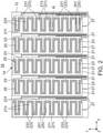
Fig. 2 is a plan view showing the touch panel ofFig. 1 . First electrodes, second electrodes, dummy electrodes and wirings are simplified and depicted. A protective layer is omitted. -
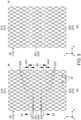
Figs. 3 (a) and 3 (b) are expanded views each of which shows a range R surrounded by a broken line in the touch panel ofFig. 2 , whereFig. 3 (a) is a diagram to which reference numerals necessary for the explanation are added, and whereFig. 3 (b) is a diagram identical toFig. 3 (a) from which the reference numerals are removed in part. -
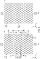
Figs. 4 (a) and 4(b) are diagrams each of which shows a first modified example of a conductive mesh shown inFigs. 3 (a) and 3 (b) , whereFig. 4 (a) is a diagram to which reference numerals necessary for the explanation are added, and whereFig. 4 (b) is a diagram identical toFig. 4 (a) from which the reference numerals are removed in part. -
Figs. 5 (a) and 5 (b) are diagrams each of which shows a second modified example of the conductive mesh shown inFigs. 3 (a) and 3 (b) , whereFig. 5 (b) is a diagram to which reference numerals necessary for the explanation are added, and whereFig. 5 (b) is a diagram identical toFig. 5 (a) from which the reference numerals are removed in part. -
Figs. 6 (a) and 6 (b) are diagrams each of which shows a third modified example of the conductive mesh shown inFigs. 3 (a) and 3 (b) , whereFig. 6 (b) is a diagram to which reference numerals necessary for the explanation are added, and whereFig. 6 (b) is a diagram identical toFig. 6 (a) from which the reference numerals are removed in part. -
Figs. 7 (a) and 7 (b) are diagrams each of which shows a fourth modified example of the conductive mesh shown inFigs. 3 (a) and 3 (b) , whereFig. 7 (b) is a diagram to which reference numerals necessary for the explanation are added, and whereFig. 7 (b) is a diagram identical toFig. 7 (a) from which the reference numerals are removed in part. -
Figs. 8 (a) and 8 (b) are diagrams each of which shows a fifth modified example of the conductive mesh shown inFigs. 3 (a) and 3 (b) , whereFig. 8 (b) is a diagram to which reference numerals necessary for the explanation are added, and whereFig. 8 (b) is a diagram identical toFig. 8 (a) from which the reference numerals are removed in part. -
Figs. 9 (a) and 9 (b) are diagrams each of which shows a sixth modified example of the conductive mesh shown inFigs. 3 (a) and 3 (b) , whereFig. 9 (b) is a diagram to which reference numerals necessary for the explanation are added, and whereFig. 9 (b) is a diagram identical toFig. 9 (a) from which the reference numerals are removed in part. -
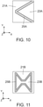
Fig. 10 is a diagram showing a modified example of the first electrode, the second electrode and the dummy electrode which are included in the touch panel ofFig. 2 . The first electrode, the second electrode and the dummy electrode are simplified. The second electrode corresponds to one of the second electrodes ofFig. 2 . -
Fig. 11 is a diagram showing another modified example of the first electrode, the second electrode and the dummy electrode which are included in the touch panel ofFig. 2 . The first electrode, the second electrode and the dummy electrode are simplified. The second electrode corresponds to one of the second electrodes ofFig. 2 . -
Fig. 12 is a plan view showing an electrode layer of a sensor portion included in a mutual capacitive system touch panel disclosed in Patent Document 1. - While the invention is susceptible of various modifications and alternative forms, specific embodiments thereof are shown by way of example in the drawings and will herein be described in detail. It should be understood, however, that the drawings and detailed description thereto are not intended to limit the invention to the particular form disclosed, but on the contrary, the intention is to cover all modifications, equivalents and alternatives falling within the spirit and scope of the present invention as defined by the appended claims.
- Referring to
Fig. 1 , a mutual capacitive system touch panel (a touch panel) 10 according to a first embodiment of the present invention is provided with abase member 12, anelectrode layer 14 formed on a surface of thebase member 12 and aprotective layer 16 provided on the surface of thebase member 12 to cover theelectrode layer 14. - In the
touch panel 10 ofFig. 1 , thebase member 12 may be a plate-like or film-like member which is made of glass or resin to be optically transparent. Theelectrode layer 14 consists of a conductive mesh 30 (seeFig. 3 ) formed on the surface of thebase member 12. Theconductive mesh 30 may be formed on the surface of thebase member 12 by printing using conductive ink or by etching a conductive layer formed on the surface of thebase member 12 by vacuum deposition. Theprotective layer 16 may be formed by spin coating or printing using ink-like resin. Alternatively, theprotective layer 16 may be formed by sticking a cover member made of glass or resin with adhesive. - Referring to
Fig. 2 , theelectrode layer 14 is provided with a plurality offirst electrodes 21, a plurality ofsecond electrodes 23, a plurality ofdummy electrodes 25 and a plurality ofwirings 27. As described later, in theelectrode layer 14 of the present embodiment, an area where each of thefirst electrodes 21 and the second electrodes 23 (afirst area 41 or a second area 43: seeFig. 3 ) is formed overlaps with an area where any one of thedummy electrodes 25 is formed (a dummy area 45: seeFig. 3 ). InFig. 2 , however, in order to show schematic arrangement of thefirst electrodes 21, thesecond electrodes 23 and thedummy electrodes 25, there is a space between each of thefirst electrodes 21 and thesecond electrodes 23 and any one of thedummy electrodes 25. - As shown in
Fig. 2 , in the present embodiment, thefirst electrodes 21 are five in number, and thesecond electrodes 23 are twenty in number. Moreover, in the present embodiment, each of thefirst electrodes 21 is combined with four of thesecond electrodes 23. Thewirings 27 are connected to thefirst electrodes 21 and thesecond electrodes 23, respectively. However, the present invention is not limited thereto. The number of thefirst electrodes 21 and the number of thesecond electrodes 23 may be freely set. In addition, the ratio of the number of thefirst electrodes 21 to the number of thesecond electrodes 23 may be freely set, where thefirst electrodes 21 and thesecond electrodes 23 are combined with each other. For example, thefirst electrodes 21 and thesecond electrodes 23 may be combined with each other one to one. - As shown in
Fig. 2 , each of thefirst electrodes 21 and thesecond electrodes 23 is formed to have comb teeth-like shape. In detail, each of thefirst electrodes 21 has a firstmain portion 211 extending along a predetermined direction and a plurality of first facingportions 213 extending from the firstmain portion 211 along a perpendicular direction perpendicular to the predetermined direction. Moreover, each of thesecond electrodes 23 has a secondmain portion 231 extending along the predetermined direction and a plurality of second facingportions 233 extending from the secondmain portion 231 along the perpendicular direction. In the present embodiment, the predetermined direction is a Y-direction, and the perpendicular direction is an X-direction. The first facingportions 213 extend from the firstmain portion 211 in a positive X-direction, and the second facingportions 233 extend from the secondmain portion 231 in a negative X-direction. - As shown in
Fig. 2 , in each of the combinations of thefirst electrodes 21 and thesecond electrodes 23, the first facingportions 213 and the second facingportions 233 are alternately arranged in the predetermined direction. In this structure, the first facingportion 213 and the second facingportion 233 which are adjacent to each other are apart from each other and face each other. With this structure, thefirst electrode 21 and each of thesecond electrodes 23 form a capacitor. - Referring to
Fig. 3 , theelectrode layer 14 consists of theconductive mesh 30. Theconductive mesh 30 has a pattern in whichspecific elements 31 are repeatedly arranged in two dimensions. In the present embodiment, thespecific element 31 has a diamond shape. Thespecific element 31 is arranged so that two diagonal lines thereof are parallel to the predetermined direction and the perpendicular direction, respectively. However, the present invention is not limited thereto. Thespecific element 31 may have a shape other than the diamond shape. - As shown in
Fig.3 , theconductive mesh 30 has discontinuities between thefirst electrode 21 and thedummy electrode 25 and between thedummy electrode 25 and thesecond electrode 23. In other words, theconductive mesh 30 is divided between thefirst electrode 21 and thedummy electrode 25 and between thedummy electrode 25 and thesecond electrode 23. The division of theconductive mesh 30 is made so that an imaginary line cannot drawn each of between thefirst electrode 21 and thedummy electrode 25 and between thedummy electrode 25 and thesecond electrode 23. - As understood from
Fig. 3 , in the predetermined direction, the first facingportion 213 of thefirst electrode 21 and the second facingportion 233 of thesecond electrode 23 which are adjacent to each other are apart from each other and face each other. Between the first facingportion 213 and the second facingportion 233, an interveningportion 251 of thedummy electrode 25 intervenes. In other words, thedummy electrode 25 has the interveningportion 251 which is located between the first facingportion 213 and the second facingportion 233 at least in part. - As shown in
Fig.3 , the first facingportion 213 of thefirst electrode 21 is formed in thefirst area 41. Thefirst area 41 is an area defined by imaginarily linking outermost ends 321 of a part of theconductive mesh 30 that forms the first facingportion 213. Moreover, the second facingportion 233 of thesecond electrode 23 is formed in thesecond area 43. Thesecond area 43 is an area defined by imaginarily linking outermost ends 323 of a part of theconductive mesh 30 that forms the second facingportion 233. - Referring to
Fig. 3 , the description will be made about thefirst area 41 and thesecond area 43. In the present embodiment, theconductive mesh 30 has the pattern in which thespecific elements 31 are repeatedly arranged in the perpendicular direction. Thespecific element 31 has a predetermined size as a maximum size in perpendicular direction. The predetermined size is equal to a length of the diagonal line of thespecific element 31 in the perpendicular direction. In the present embodiment, thefirst area 41 is formed by imaginarily linking the outermost ends 321 of the area of theconductive mesh 30 that forms the first facingportion 213, wherein the outermost ends 321 are arranged at intervals of the predetermined size in the perpendicular direction. The line linking the outermost ends 321 form an edge along the perpendicular direction. In other words, thefirst area 41 has, as an end edge in the predetermined direction, an edge straightly extending in the perpendicular direction. Moreover, thesecond area 43 is formed by imaginarily linking the outermost ends 323 of the part of theconductive mesh 30 that forms the second facingportion 233, wherein the outermost ends 323 are arranged at intervals of the predetermined size in the perpendicular direction. The line linking the outermost ends 323 form an edge along the perpendicular direction. In other words, thesecond area 43 has, as an end edge in the predetermined direction, an edge straightly extending in the perpendicular direction. - As understood from
Fig. 3 , the interveningportion 251 of thedummy electrode 25 is formed in thedummy area 45. Thedummy area 45 is an area defined by imaginarily linking outermost ends 325 and 357 of a part of theconductive mesh 30 that forms the interveningportion 251. Thedummy area 45 has afirst end area 451 and asecond end area 453 as both end areas thereof in the predetermined direction. In the present embodiment, thefirst end area 451 is an area overlapping with thefirst area 41, thesecond end area 453 is an area overlapping with thesecond area 43. - As shown in
Fig. 3 , in the present embodiment, the interveningportion 251 has a plurality of firstspecific lines 331 parallel to one another in thefirst end area 451. Each of the firstspecific lines 331 corresponds to an edge of the diamond shape of thespecific element 31. Strictly, each of the firstspecific lines 331 corresponds to a part of the edge of the diamond shape of thespecific element 31. One the other hand, the first facingportion 213 has a plurality offirst end lines 341 parallel to one another as an end portion thereof in the predetermined direction. Each of thefirst end lines 341 corresponds to an edge of the diamond shape of thespecific element 31. Strictly, each of the firstspecific lines 331 corresponds to a part of the edge of the diamond shape of thespecific element 31. Then, the firstspecific lines 331 and thefirst end lines 341 are alternately arranged in the perpendicular direction. - As shown in
Fig. 3 , the interveningportion 251 further has a plurality of secondspecific lines 333 parallel to one another in thesecond end area 453. Each of the secondspecific lines 333 corresponds to an edge of the diamond shape of thespecific element 31. Strictly, each of the secondspecific lines 333 corresponds to a part of the edge of the diamond shape of thespecific element 31. One the other hand, the second facingportion 233 has a plurality ofsecond end lines 343 parallel to one another as an end portion thereof in the predetermined direction. Each of thesecond end lines 343 corresponds to an edge of the diamond shape of thespecific element 31. Strictly, each of the secondspecific lines 333 corresponds to a part of the edge of the diamond shape of thespecific element 31. Then, the secondspecific lines 333 and thesecond end lines 343 are alternately arranged in the perpendicular direction. - As understood from
Fig. 3 , the interveningportion 251 of thedummy electrode 25 enters each of thefirst area 41 and thesecond area 43 in part in the predetermined direction. In this structure, resolution of thetouch panel 10 mainly depends on a shortest distance between thefirst electrode 21 and thesecond electrode 23 in the predetermined direction or a distance between thefirst area 41 and thesecond area 43 in the predetermined direction. On the other hand, sensitivity of thetouch panel 10 mainly depends on a maximum width of the interveningportion 251 of thedummy electrode 25 in the predetermined direction or a width of thedummy area 45 in the predetermined direction. In the present embodiment, the width size of thedummy area 45 in the predetermined direction is larger than the shortest distance size between thefirst electrode 21 and thesecond electrode 23 in the predetermined direction. Accordingly, thetouch panel 10 of the present embodiment can achieve high sensitivity at the same level as a case where an interval between thefirst electrode 21 and thesecond electrode 23 is widened without widening the interval. In other words, thetouch panel 10 according to the present embodiment can improve the sensitivity without reducing the resolution. - In the aforementioned embodiment, the conductive mesh 30 (see
Fig. 3 ) is divided to form thefirst electrode 21, thesecond electrode 23 and thedummy electrode 25. In the present invention, a method for dividing theconductive mesh 30 is not limited in the aforementioned embodiment, but various methods can be employed. - For example, in the aforementioned embodiment, as shown in
Fig. 3 , the outermost ends 321 of the part of theconductive mesh 30 that forms the first facingportion 213 are arranged at intervals of the predetermined size in the predetermined direction. However, the present invention is not limited thereto. The outermost ends 321 of the part of theconductive mesh 30 that forms the first facingportion 213 may be arranged at intervals wider than the predetermined size at least in part in the perpendicular direction. For example, as shown inFig. 4 , the outermost ends 321 of the part of theconductive mesh 30 that forms the first facingportion 213 may be arranged at intervals of the predetermined size in the perpendicular direction so that one of the intervals is wider than others (First Modification). Alternatively, as shown inFig. 5 , the outermost ends 321 of the part of theconductive mesh 30 that forms the first facingportion 213 may be arranged at intervals of twice of the predetermined size in the perpendicular direction (Second Modification). - In the first modification shown in
Fig. 4 , the outermost ends 323 of the part of theconductive mesh 30 that forms the second facingportion 233 are arranged at intervals of the predetermined size in the perpendicular direction so that one of the intervals is wider than others. Moreover, in the second modification shown inFig. 5 , the outermost ends 323 of the part of theconductive mesh 30 that forms the second facingportion 233 are arranged at intervals of twice of the predetermined size in the perpendicular direction. - Moreover, in the aforementioned embodiment, as understood from
Fig. 3 , a size of each of thefirst end area 451 and thesecond end area 453 in the predetermined direction is approximately equal to a half of a length size of the diagonal line of thespecific element 31 in the predetermined direction. However, the present invention is not limited thereto. As shown inFig. 6 , the size of each of thefirst end area 451 and thesecond end area 453 in the predetermined direction may be smaller than the half of the length size of the diagonal line of thespecific element 31 in the predetermined direction (Third Modification). Moreover, as shown inFig. 7 , the size of each of thefirst end area 451 and thesecond end area 453 in the predetermined direction may be larger than the half of the length size of the diagonal line of thespecific element 31 in the predetermined direction (Forth Modification). - Furthermore, in the aforementioned embodiment, as understood from
Fig. 3 , each of the outermost ends 325 and 327 of the part of theconductive mesh 30 that forms the interveningportion 251 corresponds to an end of an edge of the diamond of any one of thespecific elements 31. However, the present invention is not limited thereto. As shown inFig. 8 , each of the outermost ends 325 and 327 of the part of theconductive mesh 30 that forms the interveningportion 251 may be an apex of the diamond of any one of the specific elements 31 (Fifth Modification). - Furthermore, in the first embodiment, as understood from
Fig. 3 , the outermost ends 325 and 327 of the part of theconductive mesh 30 that forms the interveningportion 251 correspond to one ends of the diamonds of thespecific elements 31 different from one another, respectively. However, the present invention is not limited thereto. As shown inFig. 9 , adjacent two of the outermost ends 325 and 327 of the part of theconductive mesh 30 that forms the interveningportion 251 may correspond to ends of two edges of the diamond of the same specific element 31 (Sixth Modification). - In each of the first to sixth modifications shown in
Figs. 4 to 9 , thefirst area 41 is formed by imaginarily linking the outermost ends 321 of the part of theconductive mesh 30 that forms the first facingportion 213 at intervals of at least the predetermined size in the perpendicular direction. Similarly, thesecond area 43 is defined by imaginarily linking the outermost ends 323 of the part of theconductive mesh 30 that forms the second facingportion 233 at intervals of at least the predetermined size in the perpendicular direction. - Moreover, in each of the first to sixth modifications shown in
Figs. 4 to 9 , the interveningportion 251 of thedummy electrode 25 enters, in part, into each of thefirst area 41 and thesecond area 43 in the predetermined direction. Accordingly, also in each of these modifications, thetouch panel 10 can improve the sensitivity without reducing the resolution. - Although the specific explanation about the present invention is made above referring to the embodiments, the present invention is not limited thereto but susceptible of various modifications and alternative forms without departing from the spirit of the invention. For example, although each of the
first electrode 21 and thesecond electrode 23 is formed into the comb teeth-like shape as shown inFig. 2 in the aforementioned embodiment, the present invention is not limited thereto. In an example, as shown inFig. 10 , a second electrode 23Amay be formed into a triangle shape, and afirst electrode 21A has a shape corresponding thereto. Alternatively, as shown inFig. 11 , asecond electrode 23B may be formed into a bobbin-like shape, and afirst electrode 21B may has a shape corresponds thereto. - In the example shown in
Fig. 10 , each of two directions perpendicular to the Z-direction and intersecting with both of the X-direction and the Y-direction is the predetermined direction. Between thefirst electrode 21A and thesecond electrode 23A, adummy electrode 25A is formed. Similarly to the embodiment shown inFig. 3 or the modification shown in each ofFigs. 4 to 9 , adummy area 45 where the interveningportion 251 of thedummy electrode 25A is formed overlaps with, in each of the predetermined directions, each of afirst area 41 and asecond area 43 where thefirst electrode 21A and thesecond electrode 23A are formed, respectively. - Moreover, in the example shown in
Fig. 11 , each of four directions, i.e., the X-direction, the Y-direction and two directions perpendicular to the Z-direction and intersecting with both of the X-direction and the Y-direction, is the predetermined direction. Similarly to the embodiment shown inFig. 3 or the modification shown in each ofFigs. 4 to 9 , adummy area 45 where the interveningportion 251 of thedummy electrode 25B is formed overlaps with, in each of the predetermined directions, each of afirst area 41 and asecond area 43 where thefirst electrode 21B and thesecond electrode 23B are formed, respectively. - The present invention is based on a Japanese patent application of
JP2019-097788 - While there has been described what is believed to be the preferred embodiment of the invention, those skilled in the art will recognize that other and further modifications may be made thereto without departing from the spirit of the invention, and it is intended to claim all such embodiments that fall within the true scope of the invention.
-
- 10
- mutual capacitive system touch panel (touch panel)
- 12
- base member
- 14
- electrode layer
- 16
- protective layer
- 21, 21a, 21b
- first electrode
- 23, 23a, 23b
- second electrode
- 25, 25a, 25b
- dummy electrode
- 251
- intervening portion
- 27
- wiring
- 211
- first main portion
- 213
- first facing portion
- 231
- second main portion
- 233
- second facing portion
- 30
- conductive mesh
- 31
- specific element
- 321, 323, 325, 327
- outermost end
- 331
- first specific line
- 333
- second specific line
- 341
- first end line
- 343
- second end line
- 41
- first area
- 43
- second area
- 45
- dummy area
- 451
- first end area
- 453
- second end area
Claims (5)
- A touch panel comprising a base member and an electrode layer formed on the base member, wherein:the electrode layer is made of a conductive mesh and comprises a first electrode, a second electrode and a dummy electrode;the first electrode has a first facing portion;the first facing portion is formed in a first area;the second electrode has a second facing portion;the second facing portion is formed in a second area;the first facing portion and the second facing portion are apart from each other and face each other in a predetermined direction;the dummy electrode has an intervening portion located between the first facing portion and the second facing portion at least in part;the intervening portion is formed in a dummy area;the dummy area has a first end area and a second end area as both end areas thereof in the predetermined direction;the first area and the first end area overlap with each other; andthe second area and the second end area overlap with each other.
- The touch panel as recited in claim 1, wherein:the first area is formed by imaginarily linking outermost ends of a part of the conductive mesh that forms the first facing portion;the second area is formed by imaginarily linking outermost ends of a part of the conductive mesh that forms the second facing portion; andthe dummy area is formed by imaginarily linking outermost ends of a part of the conductive mesh that forms the intervening portion.
- The touch panel as recited in claim 2, wherein:the conductive mesh has a pattern in which specific elements are repeatedly arranged in a perpendicular direction perpendicular to the predetermined direction;the specific element has a predetermined size as a maximum size in the perpendicular direction;the first area is formed by imaginarily linking the outermost ends of the part of the conductive mesh that forms the first facing portion at intervals of at least the predetermined size in the perpendicular direction;the first area has an edge linearly extending along the perpendicular direction as an end edge in the predetermined direction;the second area is formed by imaginarily linking the outermost ends of the area of the conductive mesh that forms the second facing portion at intervals of at least the predetermined size in the predetermined direction; andthe second area has an edge linearly extending along the perpendicular direction as an end edge in the predetermined direction.
- The touch panel as recited in claim 3; wherein:the specific element has a diamond shape;the intervening portion has a plurality of first specific lines parallel to one another in the first end area;each of the first specific lines corresponds to one edge of the diamond shape of the specific element;the first facing portion has a plurality of first end lines parallel to one another as an end portion in the predetermined direction;each of the first end lines corresponds to one edge of the diamond shape of the specific element;the first specific lines and the fist end lines are alternately arranged in the perpendicular direction;the intervening portion has a plurality of second specific lines parallel to one another in the second end area;each of the second specific lines corresponds to one edge of the diamond shape of the specific element;the second facing portion has a plurality of second end lines parallel to one another as an end portion in the predetermined direction;each of the second end lines corresponds to one edge of the diamond shape of the specific element; andthe second specific lines and the second end lines are alternately arranged in the perpendicular direction.
- The touch panel as recited in claim 4, wherein:the first electrode has a first main portion extending along the predetermined direction and a plurality of the first facing portions extending from the first main portion along the perpendicular direction;the second electrode has a second main portion extending in the predetermined direction and a plurality of the second facing portions extending from the second main portion; andthe first facing portions and the second facing portions are alternately arranged in the predetermined direction.
Applications Claiming Priority (2)
| Application Number | Priority Date | Filing Date | Title |
|---|---|---|---|
| JP2019097788A JP2020194215A (en) | 2019-05-24 | 2019-05-24 | Touch panel |
| PCT/JP2020/009999 WO2020240978A1 (en) | 2019-05-24 | 2020-03-09 | Touch panel |
Publications (2)
| Publication Number | Publication Date |
|---|---|
| EP3940513A1 true EP3940513A1 (en) | 2022-01-19 |
| EP3940513A4 EP3940513A4 (en) | 2022-05-11 |
Family
ID=73547514
Family Applications (1)
| Application Number | Title | Priority Date | Filing Date |
|---|---|---|---|
| EP20813978.2A Withdrawn EP3940513A4 (en) | 2019-05-24 | 2020-03-09 | TOUCHSCREEN |
Country Status (7)
| Country | Link |
|---|---|
| US (1) | US20220197433A1 (en) |
| EP (1) | EP3940513A4 (en) |
| JP (1) | JP2020194215A (en) |
| KR (1) | KR20210136117A (en) |
| CN (1) | CN113692568A (en) |
| TW (1) | TWI725764B (en) |
| WO (1) | WO2020240978A1 (en) |
Families Citing this family (1)
| Publication number | Priority date | Publication date | Assignee | Title |
|---|---|---|---|---|
| KR20260082488A (en) | 2024-11-28 | 2026-06-05 | 서원대학교산학협력단 | Propolis night cream cosmetic and its manufacturing method |
Family Cites Families (21)
| Publication number | Priority date | Publication date | Assignee | Title |
|---|---|---|---|---|
| JP5892419B2 (en) * | 2012-01-11 | 2016-03-23 | 大日本印刷株式会社 | Touch panel sensor |
| TWI456470B (en) * | 2012-03-07 | 2014-10-11 | Himax Tech Ltd | Touch cell applied to capacitive touch panel and associated capacitive touch panel |
| CN203070265U (en) * | 2013-01-25 | 2013-07-17 | 深圳市汇顶科技股份有限公司 | Single-layer capacitance touch sensor and touch control terminal |
| US20140332256A1 (en) * | 2013-05-10 | 2014-11-13 | Ronald Steven Cok | Micro-wire electrode structure having non-linear gaps |
| JP6200582B2 (en) * | 2014-04-08 | 2017-09-20 | 株式会社フジクラ | Wiring body and wiring board |
| JP6486341B2 (en) * | 2014-05-16 | 2019-03-20 | 富士フイルム株式会社 | Conductive sheet for touch panel and capacitive touch panel |
| TWI543053B (en) * | 2014-06-19 | 2016-07-21 | 晨星半導體股份有限公司 | Touch control device |
| TWI522880B (en) * | 2014-10-27 | 2016-02-21 | 敦泰電子股份有限公司 | High-transparency and high-sensitivity touch pattern structure of capacitive touch panel |
| WO2016084449A1 (en) * | 2014-11-27 | 2016-06-02 | 富士フイルム株式会社 | Conductive film, and touch panel sensor provided with same |
| KR102408918B1 (en) * | 2015-07-15 | 2022-06-14 | 삼성디스플레이 주식회사 | Touch panel and method for manufacturing touch panel |
| TWI588728B (en) * | 2015-12-09 | 2017-06-21 | 晨星半導體股份有限公司 | Mutual capacitive touch sensing device of touch panel |
| KR102556838B1 (en) * | 2016-06-01 | 2023-07-19 | 삼성디스플레이 주식회사 | Touch panel, electronic device having the same, and method of manufacturing touch panel |
| TWI610213B (en) * | 2016-09-07 | 2018-01-01 | 晨星半導體股份有限公司 | Mutual capacitive touch panel |
| JP2018112842A (en) | 2017-01-10 | 2018-07-19 | 大日本印刷株式会社 | Touch panel sensor and display with touch position detection function |
| JPWO2018193891A1 (en) * | 2017-04-17 | 2020-02-27 | パナソニックIpマネジメント株式会社 | Touch sensor |
| JP2019003505A (en) * | 2017-06-16 | 2019-01-10 | 日立化成株式会社 | Electrostatic capacitance type touch panel and method of manufacturing the same |
| JP6886909B2 (en) * | 2017-11-06 | 2021-06-16 | 日本航空電子工業株式会社 | Touch panel production method |
| JP2019097788A (en) | 2017-11-30 | 2019-06-24 | 株式会社三洋物産 | Game machine |
| JP6998242B2 (en) * | 2018-03-08 | 2022-02-04 | ホシデン株式会社 | Resin laminate |
| CN110658957B (en) * | 2018-06-28 | 2025-12-30 | 宸美(厦门)光电有限公司 | Touch panel |
| KR102746618B1 (en) * | 2019-03-12 | 2024-12-26 | 삼성디스플레이 주식회사 | Touch sensor and display device |
-
2019
- 2019-05-24 JP JP2019097788A patent/JP2020194215A/en active Pending
-
2020
- 2020-03-09 US US17/605,376 patent/US20220197433A1/en not_active Abandoned
- 2020-03-09 CN CN202080028762.6A patent/CN113692568A/en active Pending
- 2020-03-09 KR KR1020217032954A patent/KR20210136117A/en not_active Ceased
- 2020-03-09 EP EP20813978.2A patent/EP3940513A4/en not_active Withdrawn
- 2020-03-09 WO PCT/JP2020/009999 patent/WO2020240978A1/en not_active Ceased
- 2020-03-09 TW TW109107655A patent/TWI725764B/en not_active IP Right Cessation
Also Published As
| Publication number | Publication date |
|---|---|
| JP2020194215A (en) | 2020-12-03 |
| TW202044005A (en) | 2020-12-01 |
| US20220197433A1 (en) | 2022-06-23 |
| EP3940513A4 (en) | 2022-05-11 |
| WO2020240978A1 (en) | 2020-12-03 |
| TWI725764B (en) | 2021-04-21 |
| CN113692568A (en) | 2021-11-23 |
| KR20210136117A (en) | 2021-11-16 |
Similar Documents
| Publication | Publication Date | Title |
|---|---|---|
| JP5420709B2 (en) | Touch panel electrode structure, method and touch panel | |
| KR101363361B1 (en) | Panel for sensing touch input | |
| KR101814656B1 (en) | Electronic device and single-layer mutual-capacitance touch screen thereof | |
| JP2009230735A (en) | Touch panel device | |
| WO2012077576A1 (en) | Touch panel and display device with touch panel | |
| CN1754141A (en) | Lattice touch-sensing system | |
| CN101639742A (en) | Display element with touch control screen | |
| CN101847071A (en) | Capacitive touch screen of electrodes in staggered arrangement | |
| WO2015010425A1 (en) | Capacitive touchscreen | |
| US20100207891A1 (en) | Structural improvement to touch panel | |
| TW201516820A (en) | Touch screen, touch panel, and driving method thereof | |
| CN102736768A (en) | Touch sensing unit, touch sensing element and touch sensing device | |
| US9194901B2 (en) | Sensing structure of touch panel | |
| CN109906429B (en) | Touch screen and touch display device | |
| WO2019090585A1 (en) | Touch substrate and touch control display apparatus | |
| US20120062515A1 (en) | Touch panel and the touch display device using the same | |
| CN103472961B (en) | Capacitance type touch-control panel and there is the electronic installation of this capacitance type touch-control panel | |
| US20220197433A1 (en) | Touch panel | |
| EP4030270A1 (en) | Touch panel | |
| US11340729B2 (en) | Touch substrate and display panel | |
| CN113672117A (en) | Display panel and mobile terminal | |
| CN102707834A (en) | Touch panel and manufacture method of touch sensing layer of panel | |
| TWM610103U (en) | Mutual-capacitive touch screen and touch display device with the same | |
| CN206877299U (en) | A kind of touch induction device | |
| WO2014163374A1 (en) | Capacitive touchscreen panel |
Legal Events
| Date | Code | Title | Description |
|---|---|---|---|
| STAA | Information on the status of an ep patent application or granted ep patent |
Free format text: STATUS: THE INTERNATIONAL PUBLICATION HAS BEEN MADE |
|
| PUAI | Public reference made under article 153(3) epc to a published international application that has entered the european phase |
Free format text: ORIGINAL CODE: 0009012 |
|
| STAA | Information on the status of an ep patent application or granted ep patent |
Free format text: STATUS: REQUEST FOR EXAMINATION WAS MADE |
|
| 17P | Request for examination filed |
Effective date: 20210930 |
|
| AK | Designated contracting states |
Kind code of ref document: A1 Designated state(s): AL AT BE BG CH CY CZ DE DK EE ES FI FR GB GR HR HU IE IS IT LI LT LU LV MC MK MT NL NO PL PT RO RS SE SI SK SM TR |
|
| REG | Reference to a national code |
Ref country code: DE Ref legal event code: R079 Free format text: PREVIOUS MAIN CLASS: G06F0003041000 Ipc: G06F0003044000 |
|
| A4 | Supplementary search report drawn up and despatched |
Effective date: 20220408 |
|
| RIC1 | Information provided on ipc code assigned before grant |
Ipc: G06F 3/044 20060101AFI20220404BHEP |
|
| DAV | Request for validation of the european patent (deleted) | ||
| DAX | Request for extension of the european patent (deleted) | ||
| STAA | Information on the status of an ep patent application or granted ep patent |
Free format text: STATUS: THE APPLICATION IS DEEMED TO BE WITHDRAWN |
|
| 18D | Application deemed to be withdrawn |
Effective date: 20221108 |