EP3937364A1 - Power conversion device - Google Patents
Power conversion device Download PDFInfo
- Publication number
- EP3937364A1 EP3937364A1 EP19918421.9A EP19918421A EP3937364A1 EP 3937364 A1 EP3937364 A1 EP 3937364A1 EP 19918421 A EP19918421 A EP 19918421A EP 3937364 A1 EP3937364 A1 EP 3937364A1
- Authority
- EP
- European Patent Office
- Prior art keywords
- common mode
- voltage
- power conversion
- conversion device
- mode voltage
- Prior art date
- Legal status (The legal status is an assumption and is not a legal conclusion. Google has not performed a legal analysis and makes no representation as to the accuracy of the status listed.)
- Pending
Links
Images






Classifications
-
- H—ELECTRICITY
- H02—GENERATION; CONVERSION OR DISTRIBUTION OF ELECTRIC POWER
- H02M—APPARATUS FOR CONVERSION BETWEEN AC AND AC, BETWEEN AC AND DC, OR BETWEEN DC AND DC, AND FOR USE WITH MAINS OR SIMILAR POWER SUPPLY SYSTEMS; CONVERSION OF DC OR AC INPUT POWER INTO SURGE OUTPUT POWER; CONTROL OR REGULATION THEREOF
- H02M7/00—Conversion of AC power input into DC power output; Conversion of DC power input into AC power output
- H02M7/42—Conversion of DC power input into AC power output without possibility of reversal
- H02M7/44—Conversion of DC power input into AC power output without possibility of reversal by static converters
- H02M7/48—Conversion of DC power input into AC power output without possibility of reversal by static converters using discharge tubes with control electrode or semiconductor devices with control electrode
-
- H—ELECTRICITY
- H02—GENERATION; CONVERSION OR DISTRIBUTION OF ELECTRIC POWER
- H02M—APPARATUS FOR CONVERSION BETWEEN AC AND AC, BETWEEN AC AND DC, OR BETWEEN DC AND DC, AND FOR USE WITH MAINS OR SIMILAR POWER SUPPLY SYSTEMS; CONVERSION OF DC OR AC INPUT POWER INTO SURGE OUTPUT POWER; CONTROL OR REGULATION THEREOF
- H02M1/00—Details of apparatus for conversion
- H02M1/0003—Details of control, feedback or regulation circuits
-
- H—ELECTRICITY
- H02—GENERATION; CONVERSION OR DISTRIBUTION OF ELECTRIC POWER
- H02M—APPARATUS FOR CONVERSION BETWEEN AC AND AC, BETWEEN AC AND DC, OR BETWEEN DC AND DC, AND FOR USE WITH MAINS OR SIMILAR POWER SUPPLY SYSTEMS; CONVERSION OF DC OR AC INPUT POWER INTO SURGE OUTPUT POWER; CONTROL OR REGULATION THEREOF
- H02M1/00—Details of apparatus for conversion
- H02M1/12—Arrangements for reducing harmonics from AC input or output
- H02M1/123—Suppression of common mode voltage or current
-
- H—ELECTRICITY
- H02—GENERATION; CONVERSION OR DISTRIBUTION OF ELECTRIC POWER
- H02M—APPARATUS FOR CONVERSION BETWEEN AC AND AC, BETWEEN AC AND DC, OR BETWEEN DC AND DC, AND FOR USE WITH MAINS OR SIMILAR POWER SUPPLY SYSTEMS; CONVERSION OF DC OR AC INPUT POWER INTO SURGE OUTPUT POWER; CONTROL OR REGULATION THEREOF
- H02M1/00—Details of apparatus for conversion
- H02M1/12—Arrangements for reducing harmonics from AC input or output
- H02M1/126—Arrangements for reducing harmonics from AC input or output using passive filters
-
- H—ELECTRICITY
- H02—GENERATION; CONVERSION OR DISTRIBUTION OF ELECTRIC POWER
- H02M—APPARATUS FOR CONVERSION BETWEEN AC AND AC, BETWEEN AC AND DC, OR BETWEEN DC AND DC, AND FOR USE WITH MAINS OR SIMILAR POWER SUPPLY SYSTEMS; CONVERSION OF DC OR AC INPUT POWER INTO SURGE OUTPUT POWER; CONTROL OR REGULATION THEREOF
- H02M7/00—Conversion of AC power input into DC power output; Conversion of DC power input into AC power output
- H02M7/42—Conversion of DC power input into AC power output without possibility of reversal
- H02M7/44—Conversion of DC power input into AC power output without possibility of reversal by static converters
- H02M7/48—Conversion of DC power input into AC power output without possibility of reversal by static converters using discharge tubes with control electrode or semiconductor devices with control electrode
- H02M7/4803—Conversion of DC power input into AC power output without possibility of reversal by static converters using discharge tubes with control electrode or semiconductor devices with control electrode with means for reducing DC component from AC output voltage
-
- H—ELECTRICITY
- H02—GENERATION; CONVERSION OR DISTRIBUTION OF ELECTRIC POWER
- H02M—APPARATUS FOR CONVERSION BETWEEN AC AND AC, BETWEEN AC AND DC, OR BETWEEN DC AND DC, AND FOR USE WITH MAINS OR SIMILAR POWER SUPPLY SYSTEMS; CONVERSION OF DC OR AC INPUT POWER INTO SURGE OUTPUT POWER; CONTROL OR REGULATION THEREOF
- H02M7/00—Conversion of AC power input into DC power output; Conversion of DC power input into AC power output
- H02M7/42—Conversion of DC power input into AC power output without possibility of reversal
- H02M7/44—Conversion of DC power input into AC power output without possibility of reversal by static converters
- H02M7/48—Conversion of DC power input into AC power output without possibility of reversal by static converters using discharge tubes with control electrode or semiconductor devices with control electrode
- H02M7/53—Conversion of DC power input into AC power output without possibility of reversal by static converters using discharge tubes with control electrode or semiconductor devices with control electrode using devices of a triode or transistor type requiring continuous application of a control signal
- H02M7/537—Conversion of DC power input into AC power output without possibility of reversal by static converters using discharge tubes with control electrode or semiconductor devices with control electrode using devices of a triode or transistor type requiring continuous application of a control signal using semiconductor devices only, e.g. single switched pulse inverters
- H02M7/5387—Conversion of DC power input into AC power output without possibility of reversal by static converters using discharge tubes with control electrode or semiconductor devices with control electrode using devices of a triode or transistor type requiring continuous application of a control signal using semiconductor devices only, e.g. single switched pulse inverters in a bridge configuration
- H02M7/53871—Conversion of DC power input into AC power output without possibility of reversal by static converters using discharge tubes with control electrode or semiconductor devices with control electrode using devices of a triode or transistor type requiring continuous application of a control signal using semiconductor devices only, e.g. single switched pulse inverters in a bridge configuration with automatic control of output voltage or current
-
- H—ELECTRICITY
- H02—GENERATION; CONVERSION OR DISTRIBUTION OF ELECTRIC POWER
- H02M—APPARATUS FOR CONVERSION BETWEEN AC AND AC, BETWEEN AC AND DC, OR BETWEEN DC AND DC, AND FOR USE WITH MAINS OR SIMILAR POWER SUPPLY SYSTEMS; CONVERSION OF DC OR AC INPUT POWER INTO SURGE OUTPUT POWER; CONTROL OR REGULATION THEREOF
- H02M7/00—Conversion of AC power input into DC power output; Conversion of DC power input into AC power output
- H02M7/42—Conversion of DC power input into AC power output without possibility of reversal
- H02M7/44—Conversion of DC power input into AC power output without possibility of reversal by static converters
- H02M7/48—Conversion of DC power input into AC power output without possibility of reversal by static converters using discharge tubes with control electrode or semiconductor devices with control electrode
- H02M7/53—Conversion of DC power input into AC power output without possibility of reversal by static converters using discharge tubes with control electrode or semiconductor devices with control electrode using devices of a triode or transistor type requiring continuous application of a control signal
- H02M7/537—Conversion of DC power input into AC power output without possibility of reversal by static converters using discharge tubes with control electrode or semiconductor devices with control electrode using devices of a triode or transistor type requiring continuous application of a control signal using semiconductor devices only, e.g. single switched pulse inverters
- H02M7/539—Conversion of DC power input into AC power output without possibility of reversal by static converters using discharge tubes with control electrode or semiconductor devices with control electrode using devices of a triode or transistor type requiring continuous application of a control signal using semiconductor devices only, e.g. single switched pulse inverters with automatic control of output wave form or frequency
- H02M7/5395—Conversion of DC power input into AC power output without possibility of reversal by static converters using discharge tubes with control electrode or semiconductor devices with control electrode using devices of a triode or transistor type requiring continuous application of a control signal using semiconductor devices only, e.g. single switched pulse inverters with automatic control of output wave form or frequency by pulse-width modulation
-
- H—ELECTRICITY
- H02—GENERATION; CONVERSION OR DISTRIBUTION OF ELECTRIC POWER
- H02P—CONTROL OR REGULATION OF ELECTRIC MOTORS, ELECTRIC GENERATORS OR DYNAMO-ELECTRIC CONVERTERS; CONTROLLING TRANSFORMERS, REACTORS OR CHOKE COILS
- H02P27/00—Arrangements or methods for the control of AC motors characterised by the kind of supply voltage
- H02P27/04—Arrangements or methods for the control of AC motors characterised by the kind of supply voltage using variable-frequency supply voltage, e.g. inverter or converter supply voltage
- H02P27/06—Arrangements or methods for the control of AC motors characterised by the kind of supply voltage using variable-frequency supply voltage, e.g. inverter or converter supply voltage using DC to AC converters or inverters
-
- H—ELECTRICITY
- H02—GENERATION; CONVERSION OR DISTRIBUTION OF ELECTRIC POWER
- H02M—APPARATUS FOR CONVERSION BETWEEN AC AND AC, BETWEEN AC AND DC, OR BETWEEN DC AND DC, AND FOR USE WITH MAINS OR SIMILAR POWER SUPPLY SYSTEMS; CONVERSION OF DC OR AC INPUT POWER INTO SURGE OUTPUT POWER; CONTROL OR REGULATION THEREOF
- H02M1/00—Details of apparatus for conversion
- H02M1/44—Circuits or arrangements for compensating for electromagnetic interference in converters or inverters
Definitions
- the present invention relates to a power conversion device and a scheme for cancelling a common mode voltage generated during power conversion that is based on a switching operation of a power semiconductor device represented by, for example, an inverter.
- EMI electromagnetic interference
- the source of the electromagnetic interference generated by voltage-type PWM inverters primarily, arises from a current flowing through a ground conductor.
- Japanese Patent Laying-Open No. 2001-268922 proposes a scheme in which the common mode voltage of the inverter output is suppressed using coils to reduce leakage current.
- the present invention is made to solve problems as the above, and an object of the present invention is to provide a power conversion device which achieves enhanced attenuation of the common mode voltage.
- a power conversion device for causing a power semiconductor device to perform a switching operation for power conversion according to a certain aspect of the present disclosure, the power conversion device comprising: a voltage detection means that detects a common mode voltage generated upon the switching operation of the power semiconductor device; a voltage superimposing means that superimposes the common mode voltage detected by the voltage detection means on an output of the power conversion device to cancel the common mode voltage having a frequency greater than or equal to a switching frequency generated upon the switching operation of the power semiconductor device; and a residual voltage detection means that detects the common mode voltage of the power conversion device superimposed by the voltage superimposing means.
- the voltage superimposing means includes a feedback means for adding and superimposing the common mode voltage detected by the residual voltage detection means onto the output of the power conversion device.
- the voltage detection means includes a first choke coil and a first capacitor.
- the power conversion device further includes a damper for reducing effects of resonance based on a leakage inductance of the first choke coil.
- the damper includes a second choke coil and a resistor.
- the damper further includes a second capacitor.
- the resistor and the second capacitor form a high-frequency cut filter.
- the voltage detection means further includes a fast detection circuit that detects a high-frequency component of the common mode voltage.
- the residual voltage detection means a detection capacitor that detects a common mode voltage remained in each phase of the output of the power conversion device; and a detection resistor connected in series to the detection capacitor.
- the power conversion device allows for enhanced attenuation of an output common mode voltage.
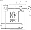
- Fig. 1 is a diagram for illustrating a configuration of a motor control system 100 according to Comparative Example.
- motor control system 100 includes an alternating-current (AC) motor 6 and a power conversion device 20.
- AC alternating-current
- Power conversion device 20 includes a voltage-type PWM inverter 4, and a common-mode suppression circuit 70 for suppressing a common mode voltage.
- Voltage-type PWM inverter 4 (also simply referred to as an inverter) is connected to a DC power supply 3, and converts a direct-current (DC) voltage into a three-phase AC voltage by a switching operation of a power semiconductor device (IGBT, MOSFET, etc.).
- a power semiconductor device IGBT, MOSFET, etc.
- the AC voltage obtained by the conversion by inverter 4 is supplied to AC motor (motor) 6 via three-phase cables 5, and a frame of AC motor 6 is connected to a ground voltage GND via a ground conductor.
- Common-mode suppression circuit 70 is disposed between inverter 4 and AC motor (motor) 6.
- Common-mode suppression circuit 70 includes: common mode voltage sensing circuit 7 which is connected to three-phase AC output terminals of inverter 4 in a star configuration and detects the common mode voltage; a common mode transformer 11 which includes a primary-side coil for receiving a common mode voltage, and secondary-side coils on three-phase cables 5; and capacitors 10A, 10B.
- Common mode voltage sensing circuit 7 includes capacitors 7A, 7B, and 7C, and choke coils 7D, 7E, and 7F. Choke coils 7D to 7F are connected to three-phase cables 5 between common mode transformer 11 and inverter 4. Choke coils 7D to 7F form nonzero-phase choke coils. Capacitors 7A to 7C are connected in series to choke coils 7D to 7F, respectively.
- Capacitors 7A to 7C are connected in a star configuration, and connected to one side of the primary-side coil included in common mode transformer 11.
- Capacitors 10A, 10B are connected in series to DC power supply 3, and a connection node NA between capacitors 10a, 10b is connected to the other side of the primary-side coil included in common mode transformer 11.
- Common mode voltage sensing circuit 7 has an output terminal connected to the primarily side of common mode transformer 11, and superimposes onto a common mode voltage having an opposite phase to the common mode voltage, according to the excitation inductance of common mode transformer 11. This is a scheme for cancelling the common mode voltage.
- common mode voltage sensing circuit 7 is, in fact, formed of choke coils, and generates leakage inductance. Due to the leakage inductance, the coupling rate of the common mode transformer is degraded, and the common mode voltage may not be suppressed sufficiently.
- Fig. 2 is a diagram for illustrating a configuration of a motor control system 1 according to Embodiment 1.
- motor control system 1 includes an AC motor 6, and a power conversion device 2 according to the present invention.
- the AC motor includes both inductor motors and synchronous motors.
- Power conversion device 2 includes a voltage-type PWM inverter 4, and a common-mode suppression circuit 17 for suppressing a common mode voltage.
- power conversion device 2 is the same, except for including common-mode suppression circuit 17, instead of common-mode suppression circuit 70.
- Common-mode suppression circuit 17 includes: a common mode voltage sensing circuit 7 which is connected to three-phase AC output terminals of inverter 4 in a star configuration, and detects a common mode voltage; common mode transformer 11 which includes a primary-side coil for receiving the common mode voltage and secondary-side coils on three-phase cables 5; a residual common mode voltage sensing circuit 8; and a feedback circuit 9.
- Common mode voltage sensing circuit 7 includes capacitors 7A, 7B, and 7C, and choke coils 7D, 7E, and 7F. Choke coils 7D to 7F are connected to three-phase cables 5 between common mode transformer 11 and inverter 4. Choke coils 7D to 7F form nonzero-phase choke coils. Capacitors 7A to 7C are connected in series to choke coils 7D to 7F, respectively.
- Capacitors 7A to 7C are connected in a star configuration, and connect to one side of the primary-side coil included in common mode transformer 11.
- Residual common mode voltage sensing circuit 8 includes capacitors 8A to 8C which are connected, in a star configuration, to three-phase cables 5 between common mode transformer 11 and AC motor 6, and detect a residual common mode voltage.
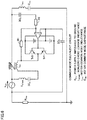
- Feedback circuit 9 further includes an operational amplifier CP, resistors R0, R1, a push-pull emitter follower circuit using a complementary transistor for power amplification, capacitors 10A, 10B, and DC power supplies 3A, 3B.
- the emitter follower circuit includes bipolar transistors Tr3, Tr4 which are connected in series to DC power supplies 3A, 3B, and whose bases are connected to an output of operational amplifier CP.
- the emitter follower circuit (bipolar transistors Tr3, Tr4) to amplify the possible output current of operational amplifier CP, it should be noted that the emitter follower circuit may not be provided.
- Capacitors 10A, 10B are connected in series to DC power supply 3, and a connection node NA between capacitors 10A, 10B is connected to one (positive) input of operational amplifier CP. Connection node NA is also connected to a connection node between DC power supplies 3A, 3B.
- Operational amplifier CP has the other (negative) input connected to residual common mode voltage sensing circuit 8 via resistor R1.
- a resistor R0 is disposed between the other (negative) input of operational amplifier CP and an output of the emitter follower circuit.
- Fig. 3 is a diagram for illustrating an equivalent circuit for a common mode of common-mode suppression circuit 17 according to Embodiment 1.
- capacitance C represents a stray capacitance between the winding and frame of the motor
- inductance L represents inductance of the entire path line
- resistor R represents the resistive component of the entire path line.
- the excitation inductance L m the transformer having a turns ratio of 1:1 is common mode transformer 11 in which the leakage inductance is ignored.
- Common mode voltage sensing circuit 7 is represented by: leakage inductance L1 of the nonzero-phase choke coil; and capacitance C2 which is the sum of capacitors 7A, 7B, and 7C.
- Feedback circuit 9 can be represented by a voltage-controlled power supply A# which receives voltage Ve and outputs voltage Vce.
- Voltage Vinv is a common mode voltage of the inverter output.
- Current Im is an excitation current of the common mode transformer.
- Current Ic is a common mode current flowing through the motor.
- Voltage Vo is a common mode voltage after the common mode voltage is suppressed.
- Common mode voltage Vinv contains zero-phase voltage component Vlow and voltage Vhi which has a component of frequency greater than or equal to the switching frequency.
- Excitation inductance Lm a combined capacitance C4 of capacitors 10A, 10B, and combined capacitance C2 which is the sum of capacitors 7A, 7B, and 7C, form a resonance circuit.
- Voltage Vc detected by common mode voltage sensing circuit 7 contains error voltage Vd resulting from the leakage inductance Ll, and is represented by the following Equation (3) using Equation (1).
- Vt Vc + Vce ⁇ Vcap
- Output Vce of voltage-controlled power supply A# compensates for the error voltage resulting from the leakage inductance.
- the suppressed common mode voltage Vo is represented by the following Equation (6), using Equation (1), Equation (3), Equation (4), and Equation (5) above.
- Input Ve of voltage-controlled power supply A# is represented by the following Equation (7), using Equation (5).
- input Ve is obtained by removing the zero-phase voltage component from common mode voltage Vo.
- Input and output voltages of voltage-controlled power supply A# are represent by Equation (8).
- Vce GVe When gain G is sufficiently large, Ve is zero due to an imaginary short.
- Voltage-controlled power supply A# operates using the zero-phase voltage component as a reference potential, and input/output only a residual component that has a small amplitude.
- the residual common mode voltage detected at capacitors 8A to 8C of residual common mode voltage sensing circuit 8 is inverted amplified by operational amplifier CP, and added to common mode transformer 11.
- the operating reference point (ground) for the operational amplifier for use in the feedback control is set to the zero-phase voltage of an output common mode voltage of the inverter, thereby allowing for the use of a lower breakdown, high-speed, inexpensive operational amplifier.
- the supply voltage of the inverter is 600 V and the switching frequency is 100 kHz. Note that no load is connected to AC motor (motor) 6.
- Gain G is set to 10.
- Fig. 4 shows diagrams for illustrating waveforms of common mode voltages.
- Fig. 4 (A) of shows a common mode voltage suppressed by common-mode suppression circuit 70 according to Comparative Example.
- Fig. 4 (B) shows a common mode voltage suppressed by common-mode suppression circuit 17 according to Embodiment 1.
- the reference potential is a neutral point of the inverter power supply.
- the amplitude of about 5.8 V, shown in Fig. 4 (A) can be reduced to the amplitude of about 0.6 V in Fig. 4 (B) .
- Fig. 5 is a diagram for illustrating attenuations of the common mode voltages.
- the attenuation at 100 kHz is 40 dB according to the configuration of Comparative Example, but is 60 dB according to the configuration of Embodiment 1. An increase in attenuation by 20 dB is observed.
- Embodiment 2 will be described with respect to a highly accurate common-mode suppression circuit.
- Embodiment 1 has been described with reference to the scheme for suppressing the influence of the coupling rate of common mode transformer 11 resulting from the leakage inductance of the choke coils included in common mode voltage sensing circuit 7.
- common mode voltage sensing circuit 7 may cause a resonance frequency in relation with AC motor 6.
- Fig. 6 is another diagram for illustrating the equivalent circuit for the common mode of common-mode suppression circuit 17 according to Embodiment 1.
- the equivalent circuit is provided with leakage inductance L d_leak of the choke coils included in common mode voltage sensing circuit 7, and motor common mode inductance Lmc and a motor common mode capacitance Cmc of AC motor (motor) 6.
- Resonance frequency based on these is calculated by the following Equation (11).
- Fig. 7 is a diagram for illustrating the gain and phase of an open-loop transfer function.
- oscillation occurs when the phase is -360 degrees and the gain is 0 dB or higher. In this example, oscillation may occur because the gain is 20 dB or higher.
- This oscillation may be a source of noise on feedback circuit 9, making it difficult for residual common mode voltage sensing circuit 8 to accurately detect the residual common mode voltage.
- Fig. 8 is a diagram for illustrating a configuration of a motor control system 1# according to Embodiment 2.
- motor control system 1# is the same, except for including a power conversion device 2#, instead of power conversion device 2.
- power conversion device 2# is the same, except for including a common-mode suppression circuit 17#, instead of common-mode suppression circuit 17.
- common-mode suppression circuit 17# is the same, except for further including a damper circuit 25.
- Damper circuit 25 is disposed between common mode transformer 11 and AC motor (motor) 6. Note that damper circuit 25 may be disclosed between inverter 4 and common mode transformer 11. Alternatively, damper circuit 25 may be provided at the earlier stage of inverter 4.
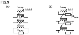
- Fig. 9 shows diagram for illustrating configurations of the damper circuits according to Embodiment 2.
- Fig. 9 (A) an example of four-phase common mode choke coils is shown.
- the turns ratio of the four is 1:1:1:1.
- One damper resistor is connected to a fourth winding.
- the reactance of the choke coil is L dump
- the resistance of the damper resistor is R dump .
- Fig. 9 (B) an example of three-phase common mode choke coils is shown.
- the turns ratio of the three is 1:1:1.
- One damper resistor is provided for each winding.
- the damper resistor is connected in parallel with the winding.
- Fig. 10 is a diagram for illustrating an equivalent circuit for the common mode of a common-mode suppression circuit 17# according to Embodiment 2.
- reactance L dump and damper resistance R dump by damper circuit 25 are connected in parallel, between common mode transformer 11 and AC motor (motor) 6.
- Fig. 11 is a diagram for illustrating the gain and phase of the resonance frequency after insertion of damper circuit 25.
- oscillation occurs when the phase is -360 degrees and the gain is 0 dB or higher.
- the oscillation can be suppressed because the gain is less than 0 dB.
- the resonance frequency can be lowered and changes in phase caused by the resonance can be alleviated by damper circuit 25.
- reactance L dump of damper circuit 25 is 300 ⁇ H
- damper resistance R dump is 1 k ⁇
- Gain G is set to 10.
- Leakage inductance L d_leak of the choke coils included in common mode voltage sensing circuit 7 is 10 ⁇ H
- the motor common mode inductance L mc of AC motor (motor) 6 is 1 ⁇ H
- the motor common mode capacitance Cmc is 500 pF.
- a simulation of the motor control system 1# is performed.
- Embodiment 3 will be described with respect to a more accurate common-mode suppression circuit.
- Embodiment 2 has been described with reference to the scheme for suppressing the resonance frequency resulting from the leakage inductance of common mode voltage sensing circuit 7.
- common mode voltage sensing circuit 7 detects a common mode voltage, using choke coils.
- Fig. 12 shows diagrams for illustrating detection of the common mode voltage of common mode voltage sensing circuit 7.
- common mode voltage sensing circuit 7 detects a common mode voltage output from an inverter 4.
- inverter 4 is a fast switching device (as one example, the switching time is about 100 ns). Choke coils included in common mode voltage sensing circuit 7 struggle to follow abrupt voltage changes, and thus may be a cause of residual common mode voltage.
- Fig. 13 is a diagram for illustrating a configuration of a motor control system 1#A according to Embodiment 3.
- motor control system 1#A compared to motor control system 1#, motor control system 1#A according to Embodiment 3 is the same, except for including a power conversion device 2#A, instead of power conversion device 2#.
- power conversion device 2#A is the same, except for including a common-mode suppression circuit 17#A, instead of common-mode suppression circuit 17#.
- common-mode suppression circuit 17#A is the same, except for including a filter circuit 30 between inverter 4 and common mode transformer 11.
- Filter circuit 30 includes a damper circuit 32 and capacitors 34, 36, and 38.
- Damper circuit 32 is the same as damper circuit 25 described with reference to Embodiment 2.
- Capacitors 34, 36, and 38 each have one side connected to a respective phase and the other sides of capacitors 34, 36, and 38 are connected in a star configuration, and connected to a ground.
- Filter circuit 30 attenuates a high-frequency component. Specifically, filter circuit 30 attenuates only high-frequency components that are a few hundreds of kHz higher than the common mode voltage. Filter circuit 30 suppresses abrupt changes in waveform of the common mode voltage to decrease the slope (dV/dt).
- filter circuit 30 since it includes the damper circuit, can reduce the resonance resulting from the leakage inductance of common mode voltage sensing circuit 7, as described with reference to Embodiment 2. In other words, a more accurate common-mode suppression circuit can be implemented.
- damper circuit 25 may further be provided. Specifically, a first damper circuit may be disposed between inverter 4 and common mode transformer 11, and a second damper circuit may be disposed between common mode transformer 11 and AC motor (motor) 6. This allows for implementation of a more accurate common-mode suppression circuit.
- Fig. 14 is a diagram for illustrating a configuration of a motor control system 1#B according to a variation of Embodiment 3.
- motor control system 1#B compared to motor control system 1#A, motor control system 1#B according to the variation of Embodiment 3 is the same, except for including a power conversion device 2#B, instead of power conversion device 2#A.
- a power conversion device 2#B is the same, except for including a common-mode suppression circuit 17#B, instead of common-mode suppression circuit 17#A.
- a common-mode suppression circuit 17#B is the same, except for including a fast detection circuit 40 between inverter 4 and common mode transformer 11.
- Fast detection circuit 40 includes resisters 42, 44, 46, and capacitors 46, 48, 50.
- Resisters 42, 44, 46 have one sides connected to respective phases and the other sides connected to capacitors 46, 48, 50, respectively.
- Capacitors 46, 48, 50 have one sides connected in series to resisters 42, 44, 46, respectively, and the other sides connected in a star configuration.
- Fast detection circuit 40 is disposed in parallel with common mode voltage sensing circuit 7, and connected to the primary-side coil of common mode transformer 11.
- Disposing fast detection circuit 40 in parallel with common mode voltage sensing circuit 7 as such allows fast detection circuit 40 to detect abrupt changes in common mode voltage output from inverter 4, allowing suppression of the residual common mode voltage. In other words, a more accurate common-mode suppression circuit can be implemented.
- Fig. 15 is a diagram for illustrating a residual common mode voltage sensing circuit according to Embodiment 4.
- a residual common mode voltage sensing circuit 8# according to Embodiment 4 is the same, except for further including resistors 8D, 8E, and 8F.
- Resistor 8D is connected in series to capacitor 8A.
- Resistor 8E is connected in series to capacitor 8B.
- Resistor 8F is connected in series to capacitor 8C.
- Embodiment 1 has been described, with reference to including resistor R1 on the input side of operational amplifier CP, the resistor is provided on the residual common mode voltage sensing circuit 8# side.
- Providing the resistors in series with the capacitors connected to the respective phases can suppress the current flowing through the capacitors.
- the current flowing at changes in line voltage can be significantly reduced. Moreover, the suppression of the current can reduce the noise, thereby allowing for implementation of a more accurate common-mode suppression circuit.
- the power conversion device which includes the voltage-type PWM inverter according to the present invention has been described with reference to applying the power conversion device to the motor control system in which an AC motor is operated, the power conversion device is also applicable as devices such as other power conversion device which generate the common mode voltage upon switching of a power semiconductor device, for example, DC-DC converters.
Landscapes
- Engineering & Computer Science (AREA)
- Power Engineering (AREA)
- Inverter Devices (AREA)
Abstract
Description
- The present invention relates to a power conversion device and a scheme for cancelling a common mode voltage generated during power conversion that is based on a switching operation of a power semiconductor device represented by, for example, an inverter.
- In recent years, for power conversion devices such as voltage-type PWM inverters which performs operative control of, for example, a motor as a load, carrier frequencies of the voltage-type PWM inverters are increased with an expansion of the range of applications of power conversion devices and enhanced characteristics of the power semiconductor devices.
- However, electromagnetic interference (EMI) generated by the voltage-type PWM inverters is a growing concern with a higher frequency of the voltage-type PWM inverters.
- The source of the electromagnetic interference generated by voltage-type PWM inverters, primarily, arises from a current flowing through a ground conductor.
- In this respect,
Japanese Patent Laying-Open No. 2001-268922 - PTL 1:
Japanese Patent Laying-Open No. 2001-268922 - However, a problem with the technology disclosed in the above patent literature is low attenuation of the output common mode voltage due to the effect of the leakage inductance of the coils.
- The present invention is made to solve problems as the above, and an object of the present invention is to provide a power conversion device which achieves enhanced attenuation of the common mode voltage.
- A power conversion device for causing a power semiconductor device to perform a switching operation for power conversion according to a certain aspect of the present disclosure, the power conversion device comprising: a voltage detection means that detects a common mode voltage generated upon the switching operation of the power semiconductor device; a voltage superimposing means that superimposes the common mode voltage detected by the voltage detection means on an output of the power conversion device to cancel the common mode voltage having a frequency greater than or equal to a switching frequency generated upon the switching operation of the power semiconductor device; and a residual voltage detection means that detects the common mode voltage of the power conversion device superimposed by the voltage superimposing means. The voltage superimposing means includes a feedback means for adding and superimposing the common mode voltage detected by the residual voltage detection means onto the output of the power conversion device. The voltage detection means includes a first choke coil and a first capacitor.
- Preferably, the power conversion device further includes a damper for reducing effects of resonance based on a leakage inductance of the first choke coil.
- Preferably, the damper includes a second choke coil and a resistor.
- Preferably, the damper further includes a second capacitor. The resistor and the second capacitor form a high-frequency cut filter.
- Preferably, the voltage detection means further includes a fast detection circuit that detects a high-frequency component of the common mode voltage.
- Preferably, the residual voltage detection means a detection capacitor that detects a common mode voltage remained in each phase of the output of the power conversion device; and a detection resistor connected in series to the detection capacitor.
- The power conversion device according to the present invention allows for enhanced attenuation of an output common mode voltage.
-
-
Fig. 1 is a diagram for illustrating a configuration of amotor control system 100 according to Comparative Example. -
Fig. 2 is a diagram for illustrating a configuration of amotor control system 1 according toEmbodiment 1. -
Fig. 3 is a diagram for illustrating an equivalent circuit for a common mode of a common-mode suppression circuit 17, according toEmbodiment 1. -
Fig. 4 shows diagrams for illustrating waveforms of common mode voltages. -
Fig. 5 is a diagram for illustrating attenuations of the common mode voltages. -
Fig. 6 is another diagram for illustrating the equivalent circuit for the common mode of common-mode suppression circuit 17 according toEmbodiment 1. -
Fig. 7 is a diagram for illustrating the gain and phase of an open-loop transfer function. -
Fig. 8 is a diagram for illustrating a configuration of amotor control system 1# according toEmbodiment 2. -
Fig. 9 shows diagrams for illustrating configurations of damper circuits according toEmbodiment 2. -
Fig. 10 is a diagram for illustrating an equivalent circuit for a common mode of a common-mode suppression circuit 17# according toEmbodiment 2. -
Fig. 11 is a diagram for illustrating the gain and phase of a resonance frequency after insertion of adamper circuit 25. -
Fig. 12 shows diagrams for illustrating detection of the common mode voltage of common modevoltage sensing circuit 7. -
Fig. 13 is a diagram for illustrating a configuration of amotor control system 1#A according toEmbodiment 3. -
Fig. 14 is a diagram for illustrating a configuration of amotor control system 1#B according to a variation ofEmbodiment 3. -
Fig. 15 is a diagram for illustrating a residual common mode voltage sensing circuit according toEmbodiment 4. - Embodiments will be described in detail, with reference to the accompanying drawings. Note that the same reference sign is used to refer to the same or corresponding component in the drawings, and description thereof will not be repeated.
- Hereinafter, embodiments according to the present invention will be described, with reference to the accompanying drawings.
-
Fig. 1 is a diagram for illustrating a configuration of amotor control system 100 according to Comparative Example. - Referring to
Fig. 1 ,motor control system 100 includes an alternating-current (AC)motor 6 and apower conversion device 20. -
Power conversion device 20 includes a voltage-type PWM inverter 4, and a common-mode suppression circuit 70 for suppressing a common mode voltage. - Voltage-type PWM inverter 4 (also simply referred to as an inverter) is connected to a
DC power supply 3, and converts a direct-current (DC) voltage into a three-phase AC voltage by a switching operation of a power semiconductor device (IGBT, MOSFET, etc.). - The AC voltage obtained by the conversion by
inverter 4 is supplied to AC motor (motor) 6 via three-phase cables 5, and a frame ofAC motor 6 is connected to a ground voltage GND via a ground conductor. - Common-
mode suppression circuit 70 is disposed betweeninverter 4 and AC motor (motor) 6. - Common-
mode suppression circuit 70 includes: common modevoltage sensing circuit 7 which is connected to three-phase AC output terminals ofinverter 4 in a star configuration and detects the common mode voltage; acommon mode transformer 11 which includes a primary-side coil for receiving a common mode voltage, and secondary-side coils on three-phase cables 5; andcapacitors - Common mode
voltage sensing circuit 7 includescapacitors choke coils Choke coils 7D to 7F are connected to three-phase cables 5 betweencommon mode transformer 11 andinverter 4.Choke coils 7D to 7F form nonzero-phase choke coils.Capacitors 7A to 7C are connected in series to chokecoils 7D to 7F, respectively. -
Capacitors 7A to 7C are connected in a star configuration, and connected to one side of the primary-side coil included incommon mode transformer 11. -
Capacitors DC power supply 3, and a connection node NA between capacitors 10a, 10b is connected to the other side of the primary-side coil included incommon mode transformer 11. - Common mode
voltage sensing circuit 7 has an output terminal connected to the primarily side ofcommon mode transformer 11, and superimposes onto a common mode voltage having an opposite phase to the common mode voltage, according to the excitation inductance ofcommon mode transformer 11. This is a scheme for cancelling the common mode voltage. - In contrast, common mode
voltage sensing circuit 7 is, in fact, formed of choke coils, and generates leakage inductance. Due to the leakage inductance, the coupling rate of the common mode transformer is degraded, and the common mode voltage may not be suppressed sufficiently. -
Fig. 2 is a diagram for illustrating a configuration of amotor control system 1 according toEmbodiment 1. - Referring to
Fig. 2 ,motor control system 1 includes anAC motor 6, and apower conversion device 2 according to the present invention. Note that the AC motor includes both inductor motors and synchronous motors. -
Power conversion device 2 includes a voltage-type PWM inverter 4, and a common-mode suppression circuit 17 for suppressing a common mode voltage. - Compared to
power conversion device 20,power conversion device 2 is the same, except for including common-mode suppression circuit 17, instead of common-mode suppression circuit 70. - Common-
mode suppression circuit 17 includes: a common modevoltage sensing circuit 7 which is connected to three-phase AC output terminals ofinverter 4 in a star configuration, and detects a common mode voltage;common mode transformer 11 which includes a primary-side coil for receiving the common mode voltage and secondary-side coils on three-phase cables 5; a residual common modevoltage sensing circuit 8; and afeedback circuit 9. - Common mode
voltage sensing circuit 7 includescapacitors coils phase cables 5 betweencommon mode transformer 11 andinverter 4. Choke coils 7D to 7F form nonzero-phase choke coils.Capacitors 7A to 7C are connected in series to chokecoils 7D to 7F, respectively. -
Capacitors 7A to 7C are connected in a star configuration, and connect to one side of the primary-side coil included incommon mode transformer 11. - Residual common mode
voltage sensing circuit 8 includescapacitors 8A to 8C which are connected, in a star configuration, to three-phase cables 5 betweencommon mode transformer 11 andAC motor 6, and detect a residual common mode voltage. -
Feedback circuit 9 further includes an operational amplifier CP, resistors R0, R1, a push-pull emitter follower circuit using a complementary transistor for power amplification,capacitors DC power supplies - The emitter follower circuit includes bipolar transistors Tr3, Tr4 which are connected in series to
DC power supplies - While this example will be described, with reference to providing the emitter follower circuit (bipolar transistors Tr3, Tr4) to amplify the possible output current of operational amplifier CP, it should be noted that the emitter follower circuit may not be provided.
-
Capacitors DC power supply 3, and a connection node NA betweencapacitors DC power supplies - Operational amplifier CP has the other (negative) input connected to residual common mode
voltage sensing circuit 8 via resistor R1. A resistor R0 is disposed between the other (negative) input of operational amplifier CP and an output of the emitter follower circuit. -
Fig. 3 is a diagram for illustrating an equivalent circuit for a common mode of common-mode suppression circuit 17 according toEmbodiment 1. - Referring to
Fig. 3 , capacitance C represents a stray capacitance between the winding and frame of the motor, inductance L represents inductance of the entire path line, and resistor R represents the resistive component of the entire path line. The excitation inductance Lm, the transformer having a turns ratio of 1:1 iscommon mode transformer 11 in which the leakage inductance is ignored. - Common mode
voltage sensing circuit 7 is represented by: leakage inductance L1 of the nonzero-phase choke coil; and capacitance C2 which is the sum ofcapacitors -
Feedback circuit 9 can be represented by a voltage-controlled power supply A# which receives voltage Ve and outputs voltage Vce. - Voltage Vinv is a common mode voltage of the inverter output. Current Im is an excitation current of the common mode transformer. Current Ic is a common mode current flowing through the motor. Voltage Vo is a common mode voltage after the common mode voltage is suppressed.
- As one phase of
inverter 4 is switched, common mode voltage Vinv output frominverter 4 changes in a stepwise manner. - Every time the
inverter 4 is switched, output zero-phase voltage ofinverter 4, that is, the common mode voltage changes in a stepwise manner. This causes a common mode current Ic to flow to a ground conductor through the stray capacitance between the winding and frame of AC motor (motor) 6. - Common mode voltage Vinv contains zero-phase voltage component Vlow and voltage Vhi which has a component of frequency greater than or equal to the switching frequency.
- Accordingly, the following Equation (1) stands.

- Excitation inductance Lm, a combined capacitance C4 of
capacitors capacitors - Resonance frequency f is represented by the following Equation (2).
[MATH 1] Where
- Voltage Vc detected by common mode
voltage sensing circuit 7 contains error voltage Vd resulting from the leakage inductance Ll, and is represented by the following Equation (3) using Equation (1). -

- According to output Vce of voltage-controlled power supply A#, the following Equation (4) is met in the equivalent circuit.
-

- Output Vce of voltage-controlled power supply A# compensates for the error voltage resulting from the leakage inductance.
- Most of the common mode voltage is compensated for by voltage Vc, and thus the amplitude of voltage Vce is sufficiently small, as compared to the amplitude of voltage Vc. Thus, the influence of voltage Vce is negligible, and excitation current Im is defined mostly by voltage Vc.
- For this reason, if resonance frequency f is set to fall between the zero-phase voltage frequency and the switching frequency, the following Equation (5) is met, in which voltage Vcap is the zero-phase voltage component Vlow.
-

- The suppressed common mode voltage Vo is represented by the following Equation (6), using Equation (1), Equation (3), Equation (4), and Equation (5) above.

- Input Ve of voltage-controlled power supply A# is represented by the following Equation (7), using Equation (5).

- In other words, input Ve is obtained by removing the zero-phase voltage component from common mode voltage Vo.
- Input and output voltages of voltage-controlled power supply A# are represent by Equation (8).

- Accordingly, the following Equation (9) is met, using Equation (7).

- Vce at this time is represented by the following Equation (10), using Equation (6).

- Voltage-controlled power supply A# operates using the zero-phase voltage component as a reference potential, and input/output only a residual component that has a small amplitude.
- Due to the resonant circuit formed of excitation inductance Lm, capacitance C2 which is the sum of
capacitors capacitors - The residual common mode voltage detected at
capacitors 8A to 8C of residual common modevoltage sensing circuit 8 is inverted amplified by operational amplifier CP, and added tocommon mode transformer 11. - These operations result in performing a feedback control so that the common mode voltage applied to an inverter load is equal to the zero-phase voltage of the inverter, and only the component of frequency higher than or equal to the switching frequency in the common mode voltage of the inverter output, is cancelled.
- The operating reference point (ground) for the operational amplifier for use in the feedback control is set to the zero-phase voltage of an output common mode voltage of the inverter, thereby allowing for the use of a lower breakdown, high-speed, inexpensive operational amplifier.
- Evaluations of attenuation characteristics of the common mode voltages of the inverters according to Comparative Example and
Embodiment 1 will be described. -
Fig. 4 shows diagrams for illustrating waveforms of common mode voltages. -
Fig. 4 (A) of shows a common mode voltage suppressed by common-mode suppression circuit 70 according to Comparative Example. -
Fig. 4 (B) shows a common mode voltage suppressed by common-mode suppression circuit 17 according toEmbodiment 1. - Note that the reference potential is a neutral point of the inverter power supply.
- As shown in the configuration, the amplitude of about 5.8 V, shown in
Fig. 4 (A) , can be reduced to the amplitude of about 0.6 V inFig. 4 (B) . -
Fig. 5 is a diagram for illustrating attenuations of the common mode voltages. - As shown in
Fig. 5 , the attenuation at 100 kHz is 40 dB according to the configuration of Comparative Example, but is 60 dB according to the configuration ofEmbodiment 1. An increase in attenuation by 20 dB is observed. - As apparent from the figure, it can be seen that the use of the common-mode suppression circuit according to
Embodiment 1 is very effective in suppressing the common mode voltage and reducing the common mode current. -
Embodiment 2 will be described with respect to a highly accurate common-mode suppression circuit. - While
Embodiment 1 has been described with reference to the scheme for suppressing the influence of the coupling rate ofcommon mode transformer 11 resulting from the leakage inductance of the choke coils included in common modevoltage sensing circuit 7. - In contrast, the leakage inductance of common mode
voltage sensing circuit 7 may cause a resonance frequency in relation withAC motor 6. -
Fig. 6 is another diagram for illustrating the equivalent circuit for the common mode of common-mode suppression circuit 17 according toEmbodiment 1. - As shown in
Fig. 6 , the equivalent circuit is provided with leakage inductance Ld_leak of the choke coils included in common modevoltage sensing circuit 7, and motor common mode inductance Lmc and a motor common mode capacitance Cmc of AC motor (motor) 6. - Resonance frequency based on these is calculated by the following Equation (11).
[MATH 2]
-
Fig. 7 is a diagram for illustrating the gain and phase of an open-loop transfer function. - As shown in
Fig. 7 , oscillation occurs when the phase is -360 degrees and the gain is 0 dB or higher. In this example, oscillation may occur because the gain is 20 dB or higher. - This oscillation may be a source of noise on
feedback circuit 9, making it difficult for residual common modevoltage sensing circuit 8 to accurately detect the residual common mode voltage. -
Fig. 8 is a diagram for illustrating a configuration of amotor control system 1# according toEmbodiment 2. - Referring to
Fig. 8 , compared tomotor control system 1,motor control system 1# is the same, except for including apower conversion device 2#, instead ofpower conversion device 2. Compared topower conversion device 2,power conversion device 2# is the same, except for including a common-mode suppression circuit 17#, instead of common-mode suppression circuit 17. Compared to common-mode suppression circuit 17, common-mode suppression circuit 17# is the same, except for further including adamper circuit 25. -
Damper circuit 25 is disposed betweencommon mode transformer 11 and AC motor (motor) 6. Note thatdamper circuit 25 may be disclosed betweeninverter 4 andcommon mode transformer 11. Alternatively,damper circuit 25 may be provided at the earlier stage ofinverter 4. -
Fig. 9 shows diagram for illustrating configurations of the damper circuits according toEmbodiment 2. - Referring to
Fig. 9 (A) , an example of four-phase common mode choke coils is shown. The turns ratio of the four is 1:1:1:1. One damper resistor is connected to a fourth winding. The reactance of the choke coil is Ldump, and the resistance of the damper resistor is Rdump. - Referring to
Fig. 9 (B) , an example of three-phase common mode choke coils is shown. The turns ratio of the three is 1:1:1. One damper resistor is provided for each winding. The damper resistor is connected in parallel with the winding. -
Fig. 10 is a diagram for illustrating an equivalent circuit for the common mode of a common-mode suppression circuit 17# according toEmbodiment 2. - As shown in
Fig. 10 , in the equivalent circuit, reactance Ldump and damper resistance Rdump bydamper circuit 25 are connected in parallel, betweencommon mode transformer 11 and AC motor (motor) 6. -
Fig. 11 is a diagram for illustrating the gain and phase of the resonance frequency after insertion ofdamper circuit 25. - As shown in
Fig. 11 , oscillation occurs when the phase is -360 degrees and the gain is 0 dB or higher. In this example, the oscillation can be suppressed because the gain is less than 0 dB. The resonance frequency can be lowered and changes in phase caused by the resonance can be alleviated bydamper circuit 25. - Note that, as one example, reactance Ldump of
damper circuit 25 is 300 µH, and damper resistance Rdump is 1 kΩ. Gain G is set to 10. Leakage inductance Ld_leak of the choke coils included in common modevoltage sensing circuit 7 is 10 µH, the motor common mode inductance Lmc of AC motor (motor) 6 is 1 µH, and the motor common mode capacitance Cmc is 500 pF. A simulation of themotor control system 1# is performed. - This allows reduction in effects of the resonance resulting from the leakage inductance of common mode
voltage sensing circuit 7, thereby allowing for implementation of a highly accurate common-mode suppression circuit. -
Embodiment 3 will be described with respect to a more accurate common-mode suppression circuit. -
Embodiment 2 has been described with reference to the scheme for suppressing the resonance frequency resulting from the leakage inductance of common modevoltage sensing circuit 7. - In contrast, common mode
voltage sensing circuit 7 detects a common mode voltage, using choke coils. -
Fig. 12 shows diagrams for illustrating detection of the common mode voltage of common modevoltage sensing circuit 7. - As shown in
Fig. 12 , common modevoltage sensing circuit 7 detects a common mode voltage output from aninverter 4. In contrast,inverter 4 is a fast switching device (as one example, the switching time is about 100 ns). Choke coils included in common modevoltage sensing circuit 7 struggle to follow abrupt voltage changes, and thus may be a cause of residual common mode voltage. -
Fig. 13 is a diagram for illustrating a configuration of amotor control system 1#A according toEmbodiment 3. - Referring to
Fig. 13 , compared tomotor control system 1#,motor control system 1#A according toEmbodiment 3 is the same, except for including apower conversion device 2#A, instead ofpower conversion device 2#. Compared topower conversion device 2#,power conversion device 2#A is the same, except for including a common-mode suppression circuit 17#A, instead of common-mode suppression circuit 17#. Compared to common-mode suppression circuit 17#, common-mode suppression circuit 17#A is the same, except for including afilter circuit 30 betweeninverter 4 andcommon mode transformer 11. -
Filter circuit 30 includes adamper circuit 32 andcapacitors -
Damper circuit 32 is the same asdamper circuit 25 described with reference toEmbodiment 2. -
Capacitors capacitors -
Filter circuit 30 attenuates a high-frequency component. Specifically,filter circuit 30 attenuates only high-frequency components that are a few hundreds of kHz higher than the common mode voltage.Filter circuit 30 suppresses abrupt changes in waveform of the common mode voltage to decrease the slope (dV/dt). - This suppresses the common mode voltage having a high-frequency component output from
inverter 4, to increase the detection accuracy of common modevoltage sensing circuit 7 and suppress the residual common mode voltage. - Moreover,
filter circuit 30, since it includes the damper circuit, can reduce the resonance resulting from the leakage inductance of common modevoltage sensing circuit 7, as described with reference toEmbodiment 2. In other words, a more accurate common-mode suppression circuit can be implemented. - While this example has been described with reference to providing
damper circuit 32, it should be noted thatdamper circuit 25 according toEmbodiment 2 may further be provided. Specifically, a first damper circuit may be disposed betweeninverter 4 andcommon mode transformer 11, and a second damper circuit may be disposed betweencommon mode transformer 11 and AC motor (motor) 6. This allows for implementation of a more accurate common-mode suppression circuit. -
Fig. 14 is a diagram for illustrating a configuration of amotor control system 1#B according to a variation ofEmbodiment 3. - Referring to
Fig. 14 , compared tomotor control system 1#A,motor control system 1#B according to the variation ofEmbodiment 3 is the same, except for including apower conversion device 2#B, instead ofpower conversion device 2#A. Compared topower conversion device 2#A, apower conversion device 2#B is the same, except for including a common-mode suppression circuit 17#B, instead of common-mode suppression circuit 17#A. Compared to common-mode suppression circuit 17#A, a common-mode suppression circuit 17#B is the same, except for including afast detection circuit 40 betweeninverter 4 andcommon mode transformer 11. -
Fast detection circuit 40 includesresisters capacitors -
Resisters capacitors Capacitors resisters -
Fast detection circuit 40 is disposed in parallel with common modevoltage sensing circuit 7, and connected to the primary-side coil ofcommon mode transformer 11. - Disposing
fast detection circuit 40 in parallel with common modevoltage sensing circuit 7 as such allowsfast detection circuit 40 to detect abrupt changes in common mode voltage output frominverter 4, allowing suppression of the residual common mode voltage. In other words, a more accurate common-mode suppression circuit can be implemented. -
Fig. 15 is a diagram for illustrating a residual common mode voltage sensing circuit according toEmbodiment 4. - Referring to
Fig. 15 , compared to residual common modevoltage sensing circuit 8, a residual common modevoltage sensing circuit 8# according toEmbodiment 4 is the same, except for further includingresistors -
Resistor 8D is connected in series tocapacitor 8A.Resistor 8E is connected in series tocapacitor 8B.Resistor 8F is connected in series tocapacitor 8C. - While
Embodiment 1 has been described, with reference to including resistor R1 on the input side of operational amplifier CP, the resistor is provided on the residual common modevoltage sensing circuit 8# side. - Providing the resistors in series with the capacitors connected to the respective phases can suppress the current flowing through the capacitors.
- The current flowing at changes in line voltage can be significantly reduced. Moreover, the suppression of the current can reduce the noise, thereby allowing for implementation of a more accurate common-mode suppression circuit.
- The presently disclosed embodiments should be considered in all aspects as illustrative and not restrictive. The scope of the present invention is indicated by the appended claims, rather than by the above description, and all changes that come within the scope of the claims and the meaning and range of equivalency of the claims are intended to be embraced within their scope.
- While the power conversion device which includes the voltage-type PWM inverter according to the present invention has been described with reference to applying the power conversion device to the motor control system in which an AC motor is operated, the power conversion device is also applicable as devices such as other power conversion device which generate the common mode voltage upon switching of a power semiconductor device, for example, DC-DC converters.
- 1, 1# motor control system; 2, 2# power conversion device; 3, 3A, 3B DC power supply; 4 inverter; 5 three-phase cables; 6 AC motor; 7 common mode voltage sensing circuit; 8, 8# residual common mode voltage sensing circuit; 17, 17#, 17#A, 17#B common-mode suppression circuit; 10, 10A, 10B capacitor; 11 common mode transformer; and 25 damper circuit.
Claims (6)
- A power conversion device for causing a power semiconductor device to perform a switching operation for power conversion, the power conversion device comprising:a voltage detection means that detects a common mode voltage generated upon the switching operation of the power semiconductor device;a voltage superimposing means that superimposes the common mode voltage detected by the voltage detection means on an output of the power conversion device to cancel the common mode voltage having a frequency greater than or equal to a switching frequency generated upon the switching operation of the power semiconductor device; anda residual voltage detection means that detects the common mode voltage of the power conversion device superimposed by the voltage superimposing means, whereinthe voltage superimposing means includes a feedback means for adding and superimposing the common mode voltage detected by the residual voltage detection means onto the output of the power conversion device, andthe voltage detection means includes a first choke coil and a first capacitor.
- The power conversion device according to claim 1, further comprising a damper for reducing effects of resonance based on a leakage inductance of the first choke coil.
- The power conversion device according to claim 2, wherein
the damper includes a second choke coil and a resistor. - The power conversion device according to claim 3, whereinthe damper further includes a second capacitor, andthe resistor and the second capacitor form a high-frequency cut filter.
- The power conversion device according to any of claims 1 to 4, wherein
the voltage detection means further includes a fast detection circuit that detects a high-frequency component of the common mode voltage. - The power conversion device according to claim 1, wherein
the residual voltage detection means includes:a detection capacitor that detects a common mode voltage remained in each phase of the output of the power conversion device; anda detection resistor connected in series to the detection capacitor.
Applications Claiming Priority (1)
| Application Number | Priority Date | Filing Date | Title |
|---|---|---|---|
| PCT/JP2019/009163 WO2020179064A1 (en) | 2019-03-07 | 2019-03-07 | Power conversion device |
Publications (2)
| Publication Number | Publication Date |
|---|---|
| EP3937364A1 true EP3937364A1 (en) | 2022-01-12 |
| EP3937364A4 EP3937364A4 (en) | 2022-10-05 |
Family
ID=72338437
Family Applications (1)
| Application Number | Title | Priority Date | Filing Date |
|---|---|---|---|
| EP19918421.9A Pending EP3937364A4 (en) | 2019-03-07 | 2019-03-07 | POWER CONVERSION DEVICE |
Country Status (7)
| Country | Link |
|---|---|
| US (1) | US11218069B2 (en) |
| EP (1) | EP3937364A4 (en) |
| JP (1) | JP6803478B1 (en) |
| KR (1) | KR102509155B1 (en) |
| CN (1) | CN112514241B (en) |
| CA (1) | CA3103081C (en) |
| WO (1) | WO2020179064A1 (en) |
Families Citing this family (7)
| Publication number | Priority date | Publication date | Assignee | Title |
|---|---|---|---|---|
| CN112771776B (en) * | 2018-09-27 | 2024-11-08 | Abb电动汽车有限责任公司 | Device for converting between AC power and DC power |
| US20230231490A1 (en) * | 2020-09-04 | 2023-07-20 | Mitsubishi Electric Corporation | Power converter and air conditioner |
| CN116391316A (en) * | 2020-11-11 | 2023-07-04 | 三菱电机株式会社 | noise filter |
| WO2022255828A1 (en) * | 2021-06-04 | 2022-12-08 | 이엠코어텍 주식회사 | Active compensation device providing electromagnetic wave noise data |
| JP7802547B2 (en) * | 2022-01-19 | 2026-01-20 | サンデン株式会社 | Active filter device and electric compressor equipped with same |
| CN115333502A (en) * | 2022-10-13 | 2022-11-11 | 湖北工业大学 | Multistage parallel active common mode interference filter and control method |
| US12266937B2 (en) * | 2022-11-02 | 2025-04-01 | Switched Source PB, LLC | High speed protection for phase balancer with zig-zag transformer |
Family Cites Families (23)
| Publication number | Priority date | Publication date | Assignee | Title |
|---|---|---|---|---|
| DE29506951U1 (en) * | 1995-04-25 | 1995-06-22 | Siemens AG, 80333 München | Circuitry for interference suppression |
| JPH1042585A (en) * | 1996-05-21 | 1998-02-13 | Toshiba Corp | Inverter device of refrigeration cycle device and refrigeration cycle device |
| JP2863833B2 (en) * | 1996-09-18 | 1999-03-03 | 岡山大学長 | Active common mode canceller |
| JP3489659B2 (en) | 1998-04-13 | 2004-01-26 | 矢崎総業株式会社 | Solid electrolyte type carbon dioxide gas sensor and its correction method |
| JP2000201044A (en) * | 1999-01-07 | 2000-07-18 | Mitsubishi Electric Corp | Common mode noise suppression device |
| JP2001268922A (en) * | 2000-03-15 | 2001-09-28 | Yaskawa Electric Corp | Power converter |
| JP2001268322A (en) | 2000-03-21 | 2001-09-28 | Murata Mach Ltd | Image reading device |
| KR100555380B1 (en) * | 2001-08-21 | 2006-02-24 | 가부시끼가이샤 히다치 세이사꾸쇼 | Power converter |
| KR100974619B1 (en) * | 2003-09-15 | 2010-08-06 | 현대중공업 주식회사 | Filter design method and motor input overvoltage suppressor in inverter system |
| JP2007181341A (en) * | 2005-12-28 | 2007-07-12 | Yaskawa Electric Corp | Converter device |
| TWI442621B (en) * | 2007-01-19 | 2014-06-21 | Murata Manufacturing Co | High frequency parts |
| JP2008236817A (en) | 2007-03-16 | 2008-10-02 | Yaskawa Electric Corp | Common mode transformer, common mode filter and filter device |
| JP2009148078A (en) * | 2007-12-14 | 2009-07-02 | Toshiba Corp | Noise filter |
| JP5263663B2 (en) * | 2008-08-28 | 2013-08-14 | 富士電機株式会社 | Conductive noise filter |
| WO2011021485A1 (en) * | 2009-08-19 | 2011-02-24 | 株式会社安川電機 | Output filter and electric motor drive system provided therewith |
| JP5634102B2 (en) * | 2010-04-06 | 2014-12-03 | 株式会社東芝 | Grid interconnection inverter |
| CN102714469B (en) * | 2010-01-13 | 2015-01-21 | 株式会社东芝 | System combined inverter |
| JP5705144B2 (en) * | 2012-01-27 | 2015-04-22 | 三菱電機株式会社 | High frequency current reduction device and detection transformer |
| US9270159B2 (en) * | 2012-08-07 | 2016-02-23 | Hamilton Sundstrand Corporation | EMI filter using active damping with frequency dependant impedance |
| FR3002094B1 (en) * | 2013-02-13 | 2016-12-09 | Valeo Systemes De Controle Moteur | DEVICE AND METHOD FOR FILTERING ELECTROMAGNETIC INTERFERENCE |
| JP5993886B2 (en) * | 2014-03-04 | 2016-09-14 | 株式会社豊田中央研究所 | Noise filter |
| US10177702B2 (en) * | 2015-08-12 | 2019-01-08 | Samsung Electronics Co., Ltd. | Conduction noise filtering circuit, inverting device, and compressor |
| JP6491349B2 (en) * | 2015-11-06 | 2019-03-27 | 国立大学法人北海道大学 | Power converter |
-
2019
- 2019-03-07 WO PCT/JP2019/009163 patent/WO2020179064A1/en not_active Ceased
- 2019-03-07 CA CA3103081A patent/CA3103081C/en active Active
- 2019-03-07 EP EP19918421.9A patent/EP3937364A4/en active Pending
- 2019-03-07 KR KR1020217002609A patent/KR102509155B1/en active Active
- 2019-03-07 CN CN201980049829.1A patent/CN112514241B/en active Active
- 2019-03-07 US US17/265,022 patent/US11218069B2/en active Active
- 2019-03-07 JP JP2019541372A patent/JP6803478B1/en active Active
Also Published As
| Publication number | Publication date |
|---|---|
| CN112514241A (en) | 2021-03-16 |
| US11218069B2 (en) | 2022-01-04 |
| WO2020179064A1 (en) | 2020-09-10 |
| JPWO2020179064A1 (en) | 2021-03-18 |
| CA3103081C (en) | 2023-04-25 |
| CN112514241B (en) | 2024-09-03 |
| KR102509155B1 (en) | 2023-03-10 |
| JP6803478B1 (en) | 2020-12-23 |
| KR20210024125A (en) | 2021-03-04 |
| CA3103081A1 (en) | 2020-09-10 |
| EP3937364A4 (en) | 2022-10-05 |
| US20210313873A1 (en) | 2021-10-07 |
Similar Documents
| Publication | Publication Date | Title |
|---|---|---|
| US11218069B2 (en) | Power conversion device | |
| JP6491349B2 (en) | Power converter | |
| JP2863833B2 (en) | Active common mode canceller | |
| EP2787618B1 (en) | Voltage fed feed forward active EMI filter | |
| Chen et al. | A novel inverter-output passive filter for reducing both differential-and common-mode $ dv/dt $ at the motor terminals in PWM drive systems | |
| US6775157B2 (en) | Closed loop active EMI filter for reducing common or differential noise based on an error value | |
| JP3428588B2 (en) | Active filter to reduce common mode current | |
| US8649193B2 (en) | Leakage current reducing apparatus | |
| EP1289108B1 (en) | Apparatus for noise current reduction in power converters | |
| JP2004534500A (en) | Active Common Mode EMI Filter for Eliminating Conducted Electromagnetic Interference for Eliminating Impedance of Conducted Electromagnetic Devices | |
| JP2000201044A (en) | Common mode noise suppression device | |
| Han et al. | Hybrid common-mode EMI filter design for electric vehicle traction inverters | |
| Liu et al. | Impacts of high frequency, high di/dt, dv/dt environment on sensing quality of GaN based converters and their mitigation | |
| JPH08237936A (en) | Noise filter of voltage source inverter | |
| JP3468262B2 (en) | Three-phase voltage source inverter | |
| Paipodamonchai | A study of an active EMI filter for suppression of leakage current in motor drive systems | |
| Wang et al. | Hybrid EMI filter design for common mode EMI suppression in a motor drive system | |
| Khun et al. | Passive EMI filter performance improvements with common mode voltage cancellation technique for PWM inverter | |
| Miyata et al. | Circuit-Balanced Flyback Converter Eliminating the Need for an Isolated Auxiliary Supply for Gate Driver IC | |
| Khun et al. | A simplified active Input EMI filter of common-mode voltage cancellation for induction motor drive | |
| Yildirmaz | Simulation-Based Characterization of Conducted EMI in Phase-Shifted PWM DC–DC Converters with Load-Dependent Behavior |
Legal Events
| Date | Code | Title | Description |
|---|---|---|---|
| STAA | Information on the status of an ep patent application or granted ep patent |
Free format text: STATUS: THE INTERNATIONAL PUBLICATION HAS BEEN MADE |
|
| PUAI | Public reference made under article 153(3) epc to a published international application that has entered the european phase |
Free format text: ORIGINAL CODE: 0009012 |
|
| STAA | Information on the status of an ep patent application or granted ep patent |
Free format text: STATUS: REQUEST FOR EXAMINATION WAS MADE |
|
| 17P | Request for examination filed |
Effective date: 20201221 |
|
| AK | Designated contracting states |
Kind code of ref document: A1 Designated state(s): AL AT BE BG CH CY CZ DE DK EE ES FI FR GB GR HR HU IE IS IT LI LT LU LV MC MK MT NL NO PL PT RO RS SE SI SK SM TR |
|
| DAV | Request for validation of the european patent (deleted) | ||
| DAX | Request for extension of the european patent (deleted) | ||
| REG | Reference to a national code |
Ref country code: DE Ref legal event code: R079 Free format text: PREVIOUS MAIN CLASS: H02M0007480000 Ipc: H02M0007538700 |
|
| A4 | Supplementary search report drawn up and despatched |
Effective date: 20220905 |
|
| RIC1 | Information provided on ipc code assigned before grant |
Ipc: H02M 7/5395 20060101ALI20220830BHEP Ipc: H02M 1/44 20070101ALI20220830BHEP Ipc: H02M 1/12 20060101ALI20220830BHEP Ipc: H02M 7/5387 20070101AFI20220830BHEP |
|
| STAA | Information on the status of an ep patent application or granted ep patent |
Free format text: STATUS: EXAMINATION IS IN PROGRESS |
|
| 17Q | First examination report despatched |
Effective date: 20240307 |