EP3937010B1 - Verbesserte multiply-accumulate-vorrichtung für neuronale netze - Google Patents
Verbesserte multiply-accumulate-vorrichtung für neuronale netze Download PDFInfo
- Publication number
- EP3937010B1 EP3937010B1 EP21178338.6A EP21178338A EP3937010B1 EP 3937010 B1 EP3937010 B1 EP 3937010B1 EP 21178338 A EP21178338 A EP 21178338A EP 3937010 B1 EP3937010 B1 EP 3937010B1
- Authority
- EP
- European Patent Office
- Prior art keywords
- accumulation
- width
- value
- buffer
- group
- Prior art date
- Legal status (The legal status is an assumption and is not a legal conclusion. Google has not performed a legal analysis and makes no representation as to the accuracy of the status listed.)
- Active
Links
Images



Classifications
-
- G—PHYSICS
- G06—COMPUTING OR CALCULATING; COUNTING
- G06F—ELECTRIC DIGITAL DATA PROCESSING
- G06F7/00—Methods or arrangements for processing data by operating upon the order or content of the data handled
- G06F7/38—Methods or arrangements for performing computations using exclusively denominational number representation, e.g. using binary, ternary, decimal representation
- G06F7/48—Methods or arrangements for performing computations using exclusively denominational number representation, e.g. using binary, ternary, decimal representation using non-contact-making devices, e.g. tube, solid state device; using unspecified devices
- G06F7/491—Computations with decimal numbers radix 12 or 20.
- G06F7/498—Computations with decimal numbers radix 12 or 20. using counter-type accumulators
- G06F7/4983—Multiplying; Dividing
-
- G—PHYSICS
- G06—COMPUTING OR CALCULATING; COUNTING
- G06F—ELECTRIC DIGITAL DATA PROCESSING
- G06F5/00—Methods or arrangements for data conversion without changing the order or content of the data handled
- G06F5/01—Methods or arrangements for data conversion without changing the order or content of the data handled for shifting, e.g. justifying, scaling, normalising
- G06F5/015—Methods or arrangements for data conversion without changing the order or content of the data handled for shifting, e.g. justifying, scaling, normalising having at least two separately controlled shifting levels, e.g. using shifting matrices
-
- G—PHYSICS
- G06—COMPUTING OR CALCULATING; COUNTING
- G06F—ELECTRIC DIGITAL DATA PROCESSING
- G06F7/00—Methods or arrangements for processing data by operating upon the order or content of the data handled
- G06F7/38—Methods or arrangements for performing computations using exclusively denominational number representation, e.g. using binary, ternary, decimal representation
- G06F7/48—Methods or arrangements for performing computations using exclusively denominational number representation, e.g. using binary, ternary, decimal representation using non-contact-making devices, e.g. tube, solid state device; using unspecified devices
- G06F7/544—Methods or arrangements for performing computations using exclusively denominational number representation, e.g. using binary, ternary, decimal representation using non-contact-making devices, e.g. tube, solid state device; using unspecified devices for evaluating functions by calculation
- G06F7/5443—Sum of products
-
- G—PHYSICS
- G06—COMPUTING OR CALCULATING; COUNTING
- G06F—ELECTRIC DIGITAL DATA PROCESSING
- G06F9/00—Arrangements for program control, e.g. control units
- G06F9/06—Arrangements for program control, e.g. control units using stored programs, i.e. using an internal store of processing equipment to receive or retain programs
- G06F9/30—Arrangements for executing machine instructions, e.g. instruction decode
- G06F9/30003—Arrangements for executing specific machine instructions
- G06F9/30007—Arrangements for executing specific machine instructions to perform operations on data operands
- G06F9/3001—Arithmetic instructions
- G06F9/30014—Arithmetic instructions with variable precision
-
- G—PHYSICS
- G06—COMPUTING OR CALCULATING; COUNTING
- G06F—ELECTRIC DIGITAL DATA PROCESSING
- G06F9/00—Arrangements for program control, e.g. control units
- G06F9/06—Arrangements for program control, e.g. control units using stored programs, i.e. using an internal store of processing equipment to receive or retain programs
- G06F9/30—Arrangements for executing machine instructions, e.g. instruction decode
- G06F9/38—Concurrent instruction execution, e.g. pipeline or look ahead
- G06F9/3885—Concurrent instruction execution, e.g. pipeline or look ahead using a plurality of independent parallel functional units
- G06F9/3893—Concurrent instruction execution, e.g. pipeline or look ahead using a plurality of independent parallel functional units controlled in tandem, e.g. multiplier-accumulator
-
- G—PHYSICS
- G06—COMPUTING OR CALCULATING; COUNTING
- G06N—COMPUTING ARRANGEMENTS BASED ON SPECIFIC COMPUTATIONAL MODELS
- G06N3/00—Computing arrangements based on biological models
- G06N3/02—Neural networks
- G06N3/04—Architecture, e.g. interconnection topology
-
- G—PHYSICS
- G06—COMPUTING OR CALCULATING; COUNTING
- G06N—COMPUTING ARRANGEMENTS BASED ON SPECIFIC COMPUTATIONAL MODELS
- G06N3/00—Computing arrangements based on biological models
- G06N3/02—Neural networks
- G06N3/04—Architecture, e.g. interconnection topology
- G06N3/045—Combinations of networks
-
- G—PHYSICS
- G06—COMPUTING OR CALCULATING; COUNTING
- G06N—COMPUTING ARRANGEMENTS BASED ON SPECIFIC COMPUTATIONAL MODELS
- G06N3/00—Computing arrangements based on biological models
- G06N3/02—Neural networks
- G06N3/04—Architecture, e.g. interconnection topology
- G06N3/0464—Convolutional networks [CNN, ConvNet]
-
- G—PHYSICS
- G06—COMPUTING OR CALCULATING; COUNTING
- G06N—COMPUTING ARRANGEMENTS BASED ON SPECIFIC COMPUTATIONAL MODELS
- G06N3/00—Computing arrangements based on biological models
- G06N3/02—Neural networks
- G06N3/06—Physical realisation, i.e. hardware implementation of neural networks, neurons or parts of neurons
- G06N3/063—Physical realisation, i.e. hardware implementation of neural networks, neurons or parts of neurons using electronic means
-
- G—PHYSICS
- G06—COMPUTING OR CALCULATING; COUNTING
- G06N—COMPUTING ARRANGEMENTS BASED ON SPECIFIC COMPUTATIONAL MODELS
- G06N3/00—Computing arrangements based on biological models
- G06N3/02—Neural networks
- G06N3/06—Physical realisation, i.e. hardware implementation of neural networks, neurons or parts of neurons
- G06N3/063—Physical realisation, i.e. hardware implementation of neural networks, neurons or parts of neurons using electronic means
- G06N3/065—Analogue means
-
- G—PHYSICS
- G06—COMPUTING OR CALCULATING; COUNTING
- G06T—IMAGE DATA PROCESSING OR GENERATION, IN GENERAL
- G06T1/00—General purpose image data processing
- G06T1/20—Processor architectures; Processor configuration, e.g. pipelining
Definitions
- Document US 5 657 262 A refers to an arithmetic and logic computation device having an arithmetic and logic unit with a shifter on at least one input.
- the computation device which includes a multiplier, propagates a carry and applies a carry to the multiplier to carry out double precision multiply and multiply-accumulate operations.
- Document EP 0 161 089 A2 refers to a double precision multiplier that includes complement single precision multiplication means responsive to two input data.
- Document US 2002/161813 A1 refers to a multi-mode Multiplier-And-Accumulator with the double-precision Complex-Valued Multiplier-And-Accumulator as main configuration.
- Document EP 1 102 161 A2 refers to a pair of parallel 16x16 multipliers (173a, 173b) each with two 32-bit inputs and one 32-bit output.
- Document EP 1 614 027 B1 refers to a method of operating a multiplication circuit to perform multiply-accumulate (21) operations on multi-word operands is characterized by an operation sequencer programmed to direct the transfer of operand segments between RAM (15) and internal data registers (27) in a specified sequence.
- Document EP 0 890 899 B1 refers to a binary fixed-point number system in which the most significant bit is a sign bit and the decimal point is between the most significant bit and a bit which is lower by one bit than the most significant bit.
- GPUs graphics processing units
- processing pipelines may each be configured to perform a mathematical function.
- large amounts of data may be processed in parallel.
- GPUs are also often used for other applications, particularly artificial intelligence.
- Embodiments in accordance with the present invention may be embodied as an apparatus, method, or computer program product. Accordingly, the present invention may take the form of an entirely hardware embodiment, or an embodiment combining software and hardware aspects that may all generally be referred to herein as a "module” or “system.” Furthermore, the present invention may take the form of a computer program product embodied in any tangible medium of expression having computer-usable program code embodied in the medium.
- a computer-readable medium may include one or more of a portable computer diskette, a hard disk, a random access memory (RAM) device, a read-only memory (ROM) device, an erasable programmable read-only memory (EPROM or Flash memory) device, a portable compact disc read-only memory (CDROM), an optical storage device, and a magnetic storage device.
- a computer-readable medium may comprise any non-transitory medium that can contain, store, communicate, propagate, or transport the program for use by or in connection with the instruction execution system, apparatus, or device.
- Computer program code for carrying out operations of the present invention may be written in any combination of one or more programming languages, including an object-oriented programming language such as Java, Smalltalk, C++, or the like and conventional procedural programming languages, such as the "C" programming language or similar programming languages.
- the program code may execute entirely on a computer system as a stand-alone software package, on a stand-alone hardware unit, partly on a remote computer spaced some distance from the computer, or entirely on a remote computer or server.
- the remote computer may be connected to the computer through any type of network, including a local area network (LAN) or a wide area network (WAN), or the connection may be made to an external computer (for example, through the Internet using an Internet Service Provider).
- LAN local area network
- WAN wide area network
- Internet Service Provider for example, AT&T, MCI, Sprint, EarthLink, MSN, GTE, etc.
- These computer program instructions may also be stored in a non-transitory computer-readable medium that can direct a computer or other programmable data processing apparatus to function in a particular manner, such that the instructions stored in the computer-readable medium produce an article of manufacture including instruction means which implement the function/act specified in the flowchart and/or block diagram block or blocks.
- the computer program instructions may also be loaded onto a computer or other programmable data processing apparatus to cause a series of operational steps to be performed on the computer or other programmable apparatus to produce a computer implemented process such that the instructions which execute on the computer or other programmable apparatus provide processes for implementing the functions/acts specified in the flowchart and/or block diagram block or blocks.
- Fig. 1 is a block diagram illustrating an example computing device 100.
- Computing device 100 may be used to perform various procedures, such as those discussed herein.
- Computing device 100 can function as a server, a client, or any other computing entity.
- Computing device can perform various monitoring functions as discussed herein, and can execute one or more application programs, such as the application programs described herein.
- Computing device 100 can be any of a wide variety of computing devices, such as a desktop computer, a notebook computer, a server computer, a handheld computer, tablet computer and the like.
- Computing device 100 includes one or more processor(s) 102, one or more memory device(s) 104, one or more interface(s) 106, one or more mass storage device(s) 108, one or more Input/Output (I/O) device(s) 110, and a display device 130 all of which are coupled to a bus 112.
- Processor(s) 102 include one or more processors or controllers that execute instructions stored in memory device(s) 104 and/or mass storage device(s) 108.
- Processor(s) 102 may also include various types of computer-readable media, such as cache memory.
- Memory device(s) 104 include various computer-readable media, such as volatile memory (e.g., random access memory (RAM) 114) and/or nonvolatile memory (e.g., read-only memory (ROM) 116). Memory device(s) 104 may also include rewritable ROM, such as Flash memory.
- volatile memory e.g., random access memory (RAM) 114
- ROM read-only memory
- Memory device(s) 104 may also include rewritable ROM, such as Flash memory.
- Mass storage device(s) 108 include various computer readable media, such as magnetic tapes, magnetic disks, optical disks, solid-state memory (e.g., Flash memory), and so forth. As shown in Fig. 1 , a particular mass storage device is a hard disk drive 124. Various drives may also be included in mass storage device(s) 108 to enable reading from and/or writing to the various computer readable media. Mass storage device(s) 108 include removable media 126 and/or non-removable media.
- I/O device(s) 110 include various devices that allow data and/or other information to be input to or retrieved from computing device 100.
- Example I/O device(s) 110 include cursor control devices, keyboards, keypads, microphones, monitors or other display devices, speakers, printers, network interface cards, modems, lenses, CCDs or other image capture devices, and the like.
- Display device 130 includes any type of device capable of displaying information to one or more users of computing device 100. Examples of display device 130 include a monitor, display terminal, video projection device, and the like.
- a graphics-processing unit (GPU) 132 may be coupled to the processor(s) 102 and/or to the display device 130.
- the GPU may be operable to render computer generated images and perform other graphical processing.
- the GPU may include some or all of the functionality of a general-purpose processor, such as the processor(s) 102.
- the GPU may also include additional functionality specific to graphics processing.
- the GPU may include hard-coded and/or hard-wired graphics function related to coordinate transformation, shading, texturing, rasterization, and other functions helpful in rendering a computer generated image.
- Interface(s) 106 include various interfaces that allow computing device 100 to interact with other systems, devices, or computing environments.
- Example interface(s) 106 include any number of different network interfaces 120, such as interfaces to local area networks (LANs), wide area networks (WANs), wireless networks, and the Internet.
- Other interface(s) include user interface 118 and peripheral device interface 122.
- the interface(s) 106 may also include one or more user interface elements 118.
- the interface(s) 106 may also include one or more peripheral interfaces such as interfaces for printers, pointing devices (mice, track pad, etc.), keyboards, and the like.
- Bus 112 allows processor(s) 102, memory device(s) 104, interface(s) 106, mass storage device(s) 108, and I/O device(s) 110 to communicate with one another, as well as other devices or components coupled to bus 112.
- Bus 112 represents one or more of several types of bus structures, such as a system bus, PCI bus, IEEE 1394 bus, USB bus, and so forth.
- a processor 102 may include a cache 134, such as one or both of a L1 cache and an L2 cache.
- a GPU 132 may likewise include a cache 136 that may likewise include one or both of a L1 cache and an L2 cache.
- programs and other executable program components are shown herein as discrete blocks, although it is understood that such programs and components may reside at various times in different storage components of computing device 100, and are executed by processor(s) 102.
- the systems and procedures described herein can be implemented in hardware, or a combination of hardware, software, and/or firmware.
- one or more application specific integrated circuits (ASICs) can be programmed to carry out one or more of the systems and procedures described herein.
- a GPU 132, processor 102, or other computing device may include or access buffers 200, 202, such as defined in a cache 134, 316, RAM 114, or some other hardware location.
- Values stored in the buffers 200, 202 have a first width, such as 16 bits.
- other parts of a computational pipeline of a GPU 132, processor 102, or other computing device may have a smaller width, such as half of the first width, e.g., 8 bits where the first width is 16 bits.
- the values stored in the buffers 200, 202 may be values used to implement and apply a convolution neural network (CNN) or other type of neural network.
- CNN convolution neural network
- buffer 200 may store coefficients of the CNN whereas buffer 202 stores the activation values for the CNN, e.g., the values being processed according to the CNN.
- the manner in which the CNN process is performed may be according to any method known in the art with some or all multiply/accumulate operations being performed according to the methods disclosed herein.
- a sequencer 204 may read values from the buffers 200, 202 in order to perform a multiply/accumulate operation using the values stored in the buffers 200,202.
- the sequencer 204 may output a sequence of arguments 206, 208 that have the second width and are portions of first values from the buffer 200 and second values from the buffer 202.
- the manner in which the sequencer generates the arguments 206, 208 is described in detail below with respect to Figs. 3 through 5 .
- the arguments 206, 208 are input into a computational pipeline 210 that is configured to perform a multiply/accumulate operation.
- the pipeline 210 may include a multiplier 212 that multiplies the arguments 206, 208 to produce a product and a summer 214 that adds the product to contents of an accumulation buffer 216 to obtain a sum and writes the sum to the accumulation buffer 216.
- the contents of the accumulation buffer 216 may be added by an adder 218 to contents of a group accumulation buffer 220 and the result of this addition written to the group accumulation buffer 220.
- the manner in which this is performed is also described in detail below.
- the group accumulation buffer 220 may be much wider than the accumulation buffer 216. For example, where the first width is 16 bits, the second width is 8 bits, the group accumulation buffer may have a width of 48 bits whereas the accumulation buffer 216 has a width of 24 bits.
- the contents of the group accumulation buffer 220 is a result of multiplying pairs of values from the buffers 200, 202 and accumulating them.
- the contents of the group accumulation buffer 220 may then be used for any purpose desired, such as to implement a CNN or any other process that may benefit from a multiply/accumulate operation.
- the multiply/accumulate operation may be used to implement a dot product or matrix multiplication in any context in which these operations are performed.
- the bit positions for each value stored in the buffers 200, 202 may define a high portion and a low portion.
- the high portion has higher magnitude (e.g., higher significance) than the low portion and does not overlap the low portion.
- the number of bits in the high portion and the number of bits in the low portion is equal to the number of bits in each value stored in the buffers 200, 202.
- bit positions 8 through 15 may be the high portion and bit positions 0 through 7 may be the low portion, where bit position 0 is defined as the least significant bit (LSB).
- the illustrated method 300 illustrates one approach for implementing a multiply/accumulate operation.
- AH i represent the high portion at buffer position i of the buffer 200.
- BH i represent the high portion at buffer position i of the buffer 202.
- AL i represent the low portion at buffer position i of the buffer 200.
- BL i represent the low portion at buffer position i of the buffer 202.
- the method 300 may include performing 302 a multiply/accumulate operation of AH i and BH i for all buffer positions i.
- the method 300 may then include adding 304 the contents of the accumulation buffer 216 to contents of the group accumulation buffer 220 and writing the result of the addition to the group accumulation buffer 220.
- the group accumulation buffer 220 and accumulation buffer 216 may be initialized to zero such that step 304 includes simply writing the contents of the accumulation buffer 216 to the group accumulation buffer 220.
- writing may include shifting the contents of the accumulation buffer by the first width (e.g., 16 bits) prior to adding to account for the fact that the high portions AH i and BH i were processed.
- the method 300 may include performing 306 a multiply/accumulate operation of AH i and BL i for all buffer positions i.
- the method 300 may then include adding 308 the contents of the accumulation buffer 216 to contents of the group accumulation buffer 220 and writing the result of the addition to the group accumulation buffer 220.
- the accumulation buffer 216 Prior to execution of the method step 306, the accumulation buffer 216 may be initialized to zero.
- adding 308 may include shifting the contents of the accumulation buffer 216 by the second width (e.g., 8 bits) prior to adding to account for the fact that the high portions AH i were processed.
- the method 300 may include performing 310 a multiply/accumulate operation of AL i and BL i for all buffer positions i.
- the method 300 may then include adding 312 the contents of the accumulation buffer 216 to contents of the group accumulation buffer 220 and writing the result of the addition to the group accumulation buffer 220.
- the accumulation buffer 216 Prior to execution of the method step 310, the accumulation buffer 216 may be initialized to zero. As described below with respect to Fig. 5 , adding 312 will not include shifting the contents of the accumulation buffer 216 since only the low precision portions AL i , BL i were processed.
- the method 300 may include performing 314 a multiply/accumulate operation of AL i and BH i for all buffer positions i.
- the method 300 may then include adding 316 the contents of the accumulation buffer 216 to contents of the group accumulation buffer 220 and writing the result of the addition to the group accumulation buffer 220.
- the accumulation buffer 216 Prior to execution of the method step 316, the accumulation buffer 216 may be initialized to zero.
- adding 316 may include shifting the contents of the accumulation buffer 216 by the second width (e.g., 8 bits) prior to adding to account for the fact that the high portions BH i were processed.
- the group accumulation buffer 220 will store the result of performing a multiply/accumulate operations for all the values in buffer positions 0 to N - 1 in the buffers 200, 202.
- the ordering of steps 302, 306, 310, and 314 is arbitrary and these may be rearranged and substituted with for one another.
- buffer positons 0 to N - 1 are referred to but the starting address for this method and other methods described herein may be any position in memory defining the buffer.
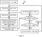
- Fig. 4 illustrates a more detailed method 400 for performing a multiply/accumulate operation for values having a first width using a computational pipeline 210 having a second width that is half of the first width.
- the method 400 may include setting 402 the position of the first argument 206 to be low, i.e., the low portion of first values in the buffer 200.
- the method 400 may further include setting 404 the position of the second argument 208 to be low, i.e. the low portion of second values in the buffer 202.
- the low portions are processed first. This is exemplary only and starting with the high portions may also be performed.
- the method 400 may include initializing 406 the current buffer position to zero and initializing the accumulator buffer 216 to zero.
- the method 400 may then include performing 408 a multiply accumulate operation for the portions of the first values at the first argument position and the portions of the second values at the second argument positions.
- the method 400 may then include adding 410 the contents of the accumulation buffer 216 to the contents of the group accumulation buffer 220 and writing the result of the addition to the group accumulation buffer 220.
- the method 400 may be preceded with initializing the group accumulation buffer 220 to zero.
- the method 400 may then include evaluating 414 whether the second argument position is high, if not, the second argument position 412 is set to high and processing continues at step 406. If so, the method 400 may include evaluating 416 whether the first argument position is high, if not, the first argument position is set 418 to high, and processing continues at step 404. If so, the method ends and the value stored in the group accumulation buffer 220 is the multiply/accumulation result for the values 0 to N - 1 in the buffers 200, 202. As noted above, 0 to N - 1 is exemplary only and any range of memory addresses may be processed according to the method 400. Note further that the range of addresses of the buffer 200 may be the same as or different from the range of addresses in the buffer 202 that are processed according to the method 400.
- the illustrated method 500 may be used when adding the contents of the accumulation buffer 216 to the contents of the group accumulation buffer 220.
- the method 500 may include evaluating 502 whether both the first and second argument positions are high. If so, the contents of the accumulation buffer 216 are left shifted 504 (assuming leftmost bit is most significant) by the first width, e.g., 16 bits, and the value as shifted at step 504 is then added 506 to the contents of the group accumulation buffer 220 and the result of the addition 506 is written to the group accumulation buffer 220.
- the first width e.g. 16 bits
- the method 500 may include evaluating 508 whether both only one of first and second argument positions are high. If so, the contents of the accumulation buffer 216 are left shifted 510 (assuming leftmost bit is most significant) by the second width, e.g., 8 bits, and the value as shifted at step 510 is then added 506 to the contents of the group accumulation buffer 220 and the result of the addition 506 is written to the group accumulation buffer 220.
- the second width e.g. 8 bits
- step 506 is performed on the un-shifted contents of the accumulation buffer 216.
Landscapes
- Engineering & Computer Science (AREA)
- Theoretical Computer Science (AREA)
- Physics & Mathematics (AREA)
- General Physics & Mathematics (AREA)
- General Engineering & Computer Science (AREA)
- Software Systems (AREA)
- Computing Systems (AREA)
- Biophysics (AREA)
- Biomedical Technology (AREA)
- Health & Medical Sciences (AREA)
- Life Sciences & Earth Sciences (AREA)
- Computational Linguistics (AREA)
- Data Mining & Analysis (AREA)
- Molecular Biology (AREA)
- Artificial Intelligence (AREA)
- Mathematical Physics (AREA)
- General Health & Medical Sciences (AREA)
- Evolutionary Computation (AREA)
- Mathematical Optimization (AREA)
- Computational Mathematics (AREA)
- Mathematical Analysis (AREA)
- Pure & Applied Mathematics (AREA)
- Neurology (AREA)
- Image Generation (AREA)
- Image Processing (AREA)
- Complex Calculations (AREA)
Claims (10)
- Vorrichtung (100) umfassend:ersten Eingabepuffer (200) mit einer ersten Breite;zweiten Eingabepuffer (202) mit der ersten Breite;Multiplikations-/Akkumulationsschaltung, die dazu konfiguriert ist, eine Multiplikations-/Akkumulationsoperation an Eingabeparametern mit einer zweiten Breite, die die Hälfte der ersten Breite beträgt, durchzuführen, wobei die Multiplikations-/Akkumulationsschaltung einen Akkumulationspuffer mit einer dritten Breite aufweist, die das Dreifache der zweiten Breite beträgt.Gruppenakkumulator (220), der dazu konfiguriert ist, eine Ausgabe der Multiplikations-/Akkumulationsschaltung zu akkumulieren, wobei der Gruppenakkumulator einen Gruppenakkumulationspuffer enthält, der eine vierte Breite aufweist, die doppelt so groß ist wie die dritte Breite;ein Sequenzer (204), der dazu konfiguriert ist, einen ersten Wert aus dem ersten Eingangspuffer und einen zweiten Wert aus dem zweiten Eingangspuffer zu lesen und den ersten Wert und den zweiten Wert zu verarbeiten, durch:Durchführen einer Multiplikations-/Akkumulationsoperation an einem hohen Bereich des ersten Werts und einem hohen Bereich des zweiten Werts unter Verwendung einer Rechenpipeline, die eine zweite Breite aufweist, um eine erste zwischenliegende Akkumulation zu erhalten;Verschieben der ersten zwischenliegenden Akkumulation um die erste Breite nach links und addieren der ersten zwischenliegende Akkumulation zu einem Gruppenakkumulationswert, der im Gruppenakkumulationspuffer gespeichert ist;Durchführen einer Multiplikations-/Akkumulationsoperation an dem hohen Bereich des ersten Werts und einem niedrigen Bereich des zweiten Werts, um eine zweie zwischenliegende Akkumulation zu erhalten;Verschieben der zweiten zwischenliegenden Akkumulation um die zweite Breite nach links und addieren der zweiten zwischenliegenden Akkumulation zu dem Gruppenakkumulationswert, der im Gruppenakkumulationspuffer gespeichert ist;Durchführen einer Multiplikations-/Akkumulationsoperation an einem niedrigen Bereich des ersten Werts und dem niedrigen Bereich des zweiten Werts, um eine dritte zwischenliegende Akkumulation zu erhalten;Addieren der dritten zwischenliegenden Akkumulation zum Gruppenakkumulationswert, der im Gruppenakkumulationspuffer gespeichert ist;Durchführen einer Multiplikations-/Akkumulationsoperation an dem niedrigen Bereich des ersten Werts und dem hohen Bereich des zweiten Werts, um eine vierte zwischenliegende Akkumulation zu erhalten; undVerschieben der vierten zwischenliegenden Akkumulation um die zweite Breite nach links und addieren der vierten zwischenliegenden Akkumulation zu dem Gruppenakkumulationswert, der im Gruppenakkumulationspuffer gespeichert ist.
- Vorrichtung (100) nach Anspruch 1, wobei der hohe Bereich eine höhere Größenordnung als der niedrige Bereich aufweist, der hohe Bereich und der niedrige Bereich nicht überlappen und eine Summe einer Anzahl von Bits im hohen Bereich und einer Anzahl von Bits im niedrigen Bereich gleich einer Anzahl von Bits in der ersten Breite ist.
- Vorrichtung (100) nach Anspruch 1, wobei die erste Breite 16 Bit und die zweite Breite 8 Bit beträgt und wobei der Gruppenakkumulationspuffer (220) eine Breite von 48 Bit aufweist.
- Vorrichtung (100) nach Anspruch 1-3, ferner umfassend eine Steuerung, die dazu programmiert ist, ein neuronales Faltungs-Netzwerk zu implementieren unter Verwendung des ersten Eingangspuffers (200), Multiplikations-/Akkumulationsschaltung, Sequenzers (204) und Gruppenakkumulators (220).
- Vorrichtung (100) nach Anspruch 1-4, ferner umfassend Grafikverarbeitungseinheit (132) enthaltend den ersten Eingangspuffer (200), Multiplikations-/Akkumulationsschaltung, Sequenzer (204) und Gruppenakkumulator (220).
- Vorrichtung (100) nach Anspruch 1-5, wobei die Multiplikations-/Akkumulationsschaltung eine erste Multiplikations-/Akkumulationsschaltung ist, wobei die Vorrichtung ferner eine Mehrzahl von Multiplikations-/Akkumulationsschaltungen umfasst, die die erste Multiplikations-/Akkumulationsschaltung enthalten.
- Verfahren (300), umfassend:Bereitstellen eines ersten Eingangspuffers, der eine erste Breite aufweist;Bereitstellen eines zweiten Eingangspuffers, der die erste Breite aufweist;Lesen, durch einen Sequenzer, eines ersten Wertes aus dem ersten Eingangspuffer undeines zweiten Wertes aus dem zweiten Eingangspuffer;Durchführen durch den Sequenzer:Multiplizieren (302) eines hohen Bereichs des ersten Werts und des hohen Bereichs des zweiten Werts in einer Rechenpipeline, die eine zweite Breite aufweist, um eine erste zwischenliegende Akkumulation zu erhalten, und Speichern der ersten zwischenliegenden Akkumulation in einem Akkumulationspuffer, der eine dritte Breite aufweist, wobei die zweite Breite die Hälfte der ersten Breite und die dritte Breite das Dreifache der zweiten Breite beträgt;Verschieben (504) der ersten zwischenliegenden Akkumulation, um die erste Breite nach links und addieren (304) der ersten zwischenliegenden Akkumulation zu einem Gruppenakkumulationswert, der in einem Gruppenakkumulationspuffer gespeichert ist, der eine vierte Breie aufweist, die doppelt so groß ist wie die dritte Breite;Multiplizieren (306) eines hohen Bereichs des ersten Werts und eines niedrigen Bereichs des zweiten Werts in der Rechenpipeline, um eine zweite zwischenliegende Akkumulation zu erhalten, und Speichern der zweiten zwischenliegenden Akkumulation im Akkumulationspuffer;Verschieben (510), der zweiten zwischenliegenden Akkumulation um die zweite Breite nach links und addieren der zweiten zwischenliegenden Akkumulation zum Gruppenakkumulationswert, der im Gruppenakkumulationspuffer gespeichert ist;Multiplizieren (310) eines niedrigen Bereichs des ersten Werts und des niedrigen Bereichs des zweiten Werts in der Rechenpipeline, um eine dritte zwischenliegende Akkumulation zu erhalten, und Speichern der dritten zwischenliegenden Akkumulation im Akkumulationspuffer;hinzufügen (312) der dritten zwischenliegenden Akkumulation zum Gruppenakkumulationswert, der im Gruppenakkumulationspuffer gespeichert ist;Multiplizieren (314) des niedrigen Bereichs des ersten Werts und des hohen Bereichs des zweiten Werts in der Rechenpipeline, um eine vierte zwischenliegende Akkumulation zu erhalten, und Speichern der vierten zwischenliegenden Akkumulation im Akkumulationspuffer;Verschieben (510) der vierten zwischenliegenden Akkumulation um die zweite Breite nach links und Addieren (316) der zweiten zwischenliegenden Akkumulation zum Gruppenakkumulationswert, der im Gruppenakkumulationspuffer gespeichert ist
- Verfahren (300) nach Anspruch 7, wobei die hohen Bereiche des ersten Werts und des zweiten Werts eine höhere Größenordnung aufweisen als die niedrigen Bereiche des ersten Werts und des zweiten Werts, wobei der hohe Bereich und der niedrige Bereich nicht überlappen und eine Summe einer Anzahl von Bits im hohen Bereich und einer Anzahl von Bits im niedrigen Bereich gleich einer Anzahl von Bits in der ersten Breite ist.
- Verfahren (300) nach Anspruch 8, wobei die erste Breite 16 Bit, die zweite Breite 8 Bit und die vierte Breite 48 Bit beträgt.
- Verfahren (300) nach Anspruch 7, ferner umfassend die Implementierung eines neuronalen Faltungs-Netzwerks (CNN) unter Verwendung des Gruppenakkumulationswerts, und wobei der erste Wert ein Koeffizient eines CNN ist und der zweite Wert ein Aktivierungswert ist, der gemäß dem CNN verarbeitet wird.
Applications Claiming Priority (1)
| Application Number | Priority Date | Filing Date | Title |
|---|---|---|---|
| US16/897,201 US11599334B2 (en) | 2020-06-09 | 2020-06-09 | Enhanced multiply accumulate device for neural networks |
Publications (2)
| Publication Number | Publication Date |
|---|---|
| EP3937010A1 EP3937010A1 (de) | 2022-01-12 |
| EP3937010B1 true EP3937010B1 (de) | 2025-03-19 |
Family
ID=76355298
Family Applications (1)
| Application Number | Title | Priority Date | Filing Date |
|---|---|---|---|
| EP21178338.6A Active EP3937010B1 (de) | 2020-06-09 | 2021-06-08 | Verbesserte multiply-accumulate-vorrichtung für neuronale netze |
Country Status (5)
| Country | Link |
|---|---|
| US (1) | US11599334B2 (de) |
| EP (1) | EP3937010B1 (de) |
| JP (1) | JP7685372B2 (de) |
| KR (1) | KR20210152957A (de) |
| CN (1) | CN113778375B (de) |
Families Citing this family (1)
| Publication number | Priority date | Publication date | Assignee | Title |
|---|---|---|---|---|
| US11908545B2 (en) * | 2022-02-24 | 2024-02-20 | Taiwan Semiconductor Manufacturing Company, Ltd. | Memory device and operating method for computing-in-memory |
Family Cites Families (12)
| Publication number | Priority date | Publication date | Assignee | Title |
|---|---|---|---|---|
| JPH061438B2 (ja) * | 1984-04-26 | 1994-01-05 | 日本電気株式会社 | 倍精度乗算器 |
| FR2718866B1 (fr) | 1994-04-19 | 1996-05-15 | Sgs Thomson Microelectronics | Dispositif de calcul arithmétique et logique et procédé de commande. |
| US6233597B1 (en) | 1997-07-09 | 2001-05-15 | Matsushita Electric Industrial Co., Ltd. | Computing apparatus for double-precision multiplication |
| JPH1173409A (ja) * | 1997-08-29 | 1999-03-16 | Matsushita Electric Ind Co Ltd | 積和演算装置および積和演算方法 |
| EP1102161A2 (de) | 1999-11-15 | 2001-05-23 | Texas Instruments Incorporated | Datenverarbeitungsanlage mit flexibler Multipliziereinheit |
| TW501344B (en) | 2001-03-06 | 2002-09-01 | Nat Science Council | Complex-valued multiplier-and-accumulator |
| FR2853425B1 (fr) * | 2003-04-07 | 2006-01-13 | Atmel Corp | Sequence de multiplication efficace pour operandes a grands nombres entiers plus larges que le materiel multiplicateur |
| US8073892B2 (en) * | 2005-12-30 | 2011-12-06 | Intel Corporation | Cryptographic system, method and multiplier |
| US10528321B2 (en) * | 2016-12-07 | 2020-01-07 | Microsoft Technology Licensing, Llc | Block floating point for neural network implementations |
| US11580353B2 (en) * | 2018-05-04 | 2023-02-14 | Apple Inc. | Neural network processor for handling differing datatypes |
| JP7129857B2 (ja) * | 2018-09-07 | 2022-09-02 | ルネサスエレクトロニクス株式会社 | 積和演算装置、積和演算方法、及びシステム |
| CN110262773B (zh) * | 2019-04-28 | 2020-08-04 | 阿里巴巴集团控股有限公司 | 一种计算机数据处理方法及装置 |
-
2020
- 2020-06-09 US US16/897,201 patent/US11599334B2/en active Active
-
2021
- 2021-06-04 JP JP2021094224A patent/JP7685372B2/ja active Active
- 2021-06-04 KR KR1020210072862A patent/KR20210152957A/ko active Pending
- 2021-06-08 CN CN202110635480.9A patent/CN113778375B/zh active Active
- 2021-06-08 EP EP21178338.6A patent/EP3937010B1/de active Active
Also Published As
| Publication number | Publication date |
|---|---|
| JP7685372B2 (ja) | 2025-05-29 |
| EP3937010A1 (de) | 2022-01-12 |
| JP2021197173A (ja) | 2021-12-27 |
| CN113778375B (zh) | 2025-12-02 |
| US20210382690A1 (en) | 2021-12-09 |
| CN113778375A (zh) | 2021-12-10 |
| US11599334B2 (en) | 2023-03-07 |
| KR20210152957A (ko) | 2021-12-16 |
Similar Documents
| Publication | Publication Date | Title |
|---|---|---|
| JP6941499B2 (ja) | ゼロ係数スキップ畳み込みニューラルネットワークエンジン | |
| CN114207579B (zh) | 包括标量处理单元的基于张量的硬件加速器 | |
| RU2263947C2 (ru) | Целочисленное умножение высокого порядка с округлением и сдвигом в архитектуре с одним потоком команд и множеством потоков данных | |
| US20040122887A1 (en) | Efficient multiplication of small matrices using SIMD registers | |
| CN110262773B (zh) | 一种计算机数据处理方法及装置 | |
| JP4349265B2 (ja) | プロセッサ | |
| JP4635087B2 (ja) | 拡張関数のための向上した浮動小数点演算部 | |
| CN111931937B (zh) | 图像处理模型的梯度更新方法、装置及系统 | |
| US9600236B2 (en) | Systems and methods for computing mathematical functions | |
| JP7685372B2 (ja) | ニューラルネットワークのための改善された乗算/累積デバイス | |
| CN110678862B (zh) | 用于硬连线乘法器电路的数据打包技术 | |
| US20230161555A1 (en) | System and method performing floating-point operations | |
| JP7811090B2 (ja) | 乗算/累算を実施するためのデバイス | |
| US20230185528A1 (en) | Optimization of arithmetic expressions | |
| JP7719621B2 (ja) | 改善されたマルチプライヤ回路 | |
| EP3239833B1 (de) | Berechnung trigonometrischer funktionen unter verwendung einer vier-eingabepunkt-produktschaltung | |
| CN112862086B (zh) | 一种神经网络运算处理方法、装置及计算机可读介质 |
Legal Events
| Date | Code | Title | Description |
|---|---|---|---|
| PUAI | Public reference made under article 153(3) epc to a published international application that has entered the european phase |
Free format text: ORIGINAL CODE: 0009012 |
|
| STAA | Information on the status of an ep patent application or granted ep patent |
Free format text: STATUS: THE APPLICATION HAS BEEN PUBLISHED |
|
| AK | Designated contracting states |
Kind code of ref document: A1 Designated state(s): AL AT BE BG CH CY CZ DE DK EE ES FI FR GB GR HR HU IE IS IT LI LT LU LV MC MK MT NL NO PL PT RO RS SE SI SK SM TR |
|
| B565 | Issuance of search results under rule 164(2) epc |
Effective date: 20211213 |
|
| STAA | Information on the status of an ep patent application or granted ep patent |
Free format text: STATUS: REQUEST FOR EXAMINATION WAS MADE |
|
| 17P | Request for examination filed |
Effective date: 20220707 |
|
| RBV | Designated contracting states (corrected) |
Designated state(s): AL AT BE BG CH CY CZ DE DK EE ES FI FR GB GR HR HU IE IS IT LI LT LU LV MC MK MT NL NO PL PT RO RS SE SI SK SM TR |
|
| GRAP | Despatch of communication of intention to grant a patent |
Free format text: ORIGINAL CODE: EPIDOSNIGR1 |
|
| STAA | Information on the status of an ep patent application or granted ep patent |
Free format text: STATUS: GRANT OF PATENT IS INTENDED |
|
| INTG | Intention to grant announced |
Effective date: 20241011 |
|
| GRAS | Grant fee paid |
Free format text: ORIGINAL CODE: EPIDOSNIGR3 |
|
| GRAA | (expected) grant |
Free format text: ORIGINAL CODE: 0009210 |
|
| STAA | Information on the status of an ep patent application or granted ep patent |
Free format text: STATUS: THE PATENT HAS BEEN GRANTED |
|
| AK | Designated contracting states |
Kind code of ref document: B1 Designated state(s): AL AT BE BG CH CY CZ DE DK EE ES FI FR GB GR HR HU IE IS IT LI LT LU LV MC MK MT NL NO PL PT RO RS SE SI SK SM TR |
|
| P01 | Opt-out of the competence of the unified patent court (upc) registered |
Free format text: CASE NUMBER: APP_6880/2025 Effective date: 20250210 |
|
| REG | Reference to a national code |
Ref country code: GB Ref legal event code: FG4D |
|
| P02 | Opt-out of the competence of the unified patent court (upc) changed |
Free format text: CASE NUMBER: APP_6955/2025 Effective date: 20250211 |
|
| REG | Reference to a national code |
Ref country code: CH Ref legal event code: EP |
|
| REG | Reference to a national code |
Ref country code: IE Ref legal event code: FG4D |
|
| REG | Reference to a national code |
Ref country code: DE Ref legal event code: R096 Ref document number: 602021027706 Country of ref document: DE |
|
| PG25 | Lapsed in a contracting state [announced via postgrant information from national office to epo] |
Ref country code: RS Free format text: LAPSE BECAUSE OF FAILURE TO SUBMIT A TRANSLATION OF THE DESCRIPTION OR TO PAY THE FEE WITHIN THE PRESCRIBED TIME-LIMIT Effective date: 20250619 |
|
| PG25 | Lapsed in a contracting state [announced via postgrant information from national office to epo] |
Ref country code: FI Free format text: LAPSE BECAUSE OF FAILURE TO SUBMIT A TRANSLATION OF THE DESCRIPTION OR TO PAY THE FEE WITHIN THE PRESCRIBED TIME-LIMIT Effective date: 20250319 |
|
| PGFP | Annual fee paid to national office [announced via postgrant information from national office to epo] |
Ref country code: GB Payment date: 20250620 Year of fee payment: 5 |
|
| REG | Reference to a national code |
Ref country code: LT Ref legal event code: MG9D |
|
| PG25 | Lapsed in a contracting state [announced via postgrant information from national office to epo] |
Ref country code: NO Free format text: LAPSE BECAUSE OF FAILURE TO SUBMIT A TRANSLATION OF THE DESCRIPTION OR TO PAY THE FEE WITHIN THE PRESCRIBED TIME-LIMIT Effective date: 20250619 |
|
| PG25 | Lapsed in a contracting state [announced via postgrant information from national office to epo] |
Ref country code: HR Free format text: LAPSE BECAUSE OF FAILURE TO SUBMIT A TRANSLATION OF THE DESCRIPTION OR TO PAY THE FEE WITHIN THE PRESCRIBED TIME-LIMIT Effective date: 20250319 |
|
| PG25 | Lapsed in a contracting state [announced via postgrant information from national office to epo] |
Ref country code: LV Free format text: LAPSE BECAUSE OF FAILURE TO SUBMIT A TRANSLATION OF THE DESCRIPTION OR TO PAY THE FEE WITHIN THE PRESCRIBED TIME-LIMIT Effective date: 20250319 |
|
| PGFP | Annual fee paid to national office [announced via postgrant information from national office to epo] |
Ref country code: FR Payment date: 20250618 Year of fee payment: 5 |
|
| PG25 | Lapsed in a contracting state [announced via postgrant information from national office to epo] |
Ref country code: GR Free format text: LAPSE BECAUSE OF FAILURE TO SUBMIT A TRANSLATION OF THE DESCRIPTION OR TO PAY THE FEE WITHIN THE PRESCRIBED TIME-LIMIT Effective date: 20250620 Ref country code: BG Free format text: LAPSE BECAUSE OF FAILURE TO SUBMIT A TRANSLATION OF THE DESCRIPTION OR TO PAY THE FEE WITHIN THE PRESCRIBED TIME-LIMIT Effective date: 20250319 |
|
| REG | Reference to a national code |
Ref country code: NL Ref legal event code: MP Effective date: 20250319 |
|
| REG | Reference to a national code |
Ref country code: AT Ref legal event code: MK05 Ref document number: 1777497 Country of ref document: AT Kind code of ref document: T Effective date: 20250319 |
|
| PG25 | Lapsed in a contracting state [announced via postgrant information from national office to epo] |
Ref country code: NL Free format text: LAPSE BECAUSE OF FAILURE TO SUBMIT A TRANSLATION OF THE DESCRIPTION OR TO PAY THE FEE WITHIN THE PRESCRIBED TIME-LIMIT Effective date: 20250319 |
|
| PG25 | Lapsed in a contracting state [announced via postgrant information from national office to epo] |
Ref country code: SE Free format text: LAPSE BECAUSE OF FAILURE TO SUBMIT A TRANSLATION OF THE DESCRIPTION OR TO PAY THE FEE WITHIN THE PRESCRIBED TIME-LIMIT Effective date: 20250319 |
|
| PG25 | Lapsed in a contracting state [announced via postgrant information from national office to epo] |
Ref country code: SM Free format text: LAPSE BECAUSE OF FAILURE TO SUBMIT A TRANSLATION OF THE DESCRIPTION OR TO PAY THE FEE WITHIN THE PRESCRIBED TIME-LIMIT Effective date: 20250319 |
|
| PG25 | Lapsed in a contracting state [announced via postgrant information from national office to epo] |
Ref country code: ES Free format text: LAPSE BECAUSE OF FAILURE TO SUBMIT A TRANSLATION OF THE DESCRIPTION OR TO PAY THE FEE WITHIN THE PRESCRIBED TIME-LIMIT Effective date: 20250319 Ref country code: PT Free format text: LAPSE BECAUSE OF FAILURE TO SUBMIT A TRANSLATION OF THE DESCRIPTION OR TO PAY THE FEE WITHIN THE PRESCRIBED TIME-LIMIT Effective date: 20250721 |
|
| PGFP | Annual fee paid to national office [announced via postgrant information from national office to epo] |
Ref country code: DE Payment date: 20250630 Year of fee payment: 5 |
|
| PG25 | Lapsed in a contracting state [announced via postgrant information from national office to epo] |
Ref country code: IT Free format text: LAPSE BECAUSE OF FAILURE TO SUBMIT A TRANSLATION OF THE DESCRIPTION OR TO PAY THE FEE WITHIN THE PRESCRIBED TIME-LIMIT Effective date: 20250319 Ref country code: PL Free format text: LAPSE BECAUSE OF FAILURE TO SUBMIT A TRANSLATION OF THE DESCRIPTION OR TO PAY THE FEE WITHIN THE PRESCRIBED TIME-LIMIT Effective date: 20250319 |
|
| PG25 | Lapsed in a contracting state [announced via postgrant information from national office to epo] |
Ref country code: AT Free format text: LAPSE BECAUSE OF FAILURE TO SUBMIT A TRANSLATION OF THE DESCRIPTION OR TO PAY THE FEE WITHIN THE PRESCRIBED TIME-LIMIT Effective date: 20250319 |
|
| PG25 | Lapsed in a contracting state [announced via postgrant information from national office to epo] |
Ref country code: CZ Free format text: LAPSE BECAUSE OF FAILURE TO SUBMIT A TRANSLATION OF THE DESCRIPTION OR TO PAY THE FEE WITHIN THE PRESCRIBED TIME-LIMIT Effective date: 20250319 Ref country code: EE Free format text: LAPSE BECAUSE OF FAILURE TO SUBMIT A TRANSLATION OF THE DESCRIPTION OR TO PAY THE FEE WITHIN THE PRESCRIBED TIME-LIMIT Effective date: 20250319 |
|
| PG25 | Lapsed in a contracting state [announced via postgrant information from national office to epo] |
Ref country code: RO Free format text: LAPSE BECAUSE OF FAILURE TO SUBMIT A TRANSLATION OF THE DESCRIPTION OR TO PAY THE FEE WITHIN THE PRESCRIBED TIME-LIMIT Effective date: 20250319 |
|
| PG25 | Lapsed in a contracting state [announced via postgrant information from national office to epo] |
Ref country code: SK Free format text: LAPSE BECAUSE OF FAILURE TO SUBMIT A TRANSLATION OF THE DESCRIPTION OR TO PAY THE FEE WITHIN THE PRESCRIBED TIME-LIMIT Effective date: 20250319 |
|
| PG25 | Lapsed in a contracting state [announced via postgrant information from national office to epo] |
Ref country code: IS Free format text: LAPSE BECAUSE OF FAILURE TO SUBMIT A TRANSLATION OF THE DESCRIPTION OR TO PAY THE FEE WITHIN THE PRESCRIBED TIME-LIMIT Effective date: 20250719 |
|
| REG | Reference to a national code |
Ref country code: DE Ref legal event code: R097 Ref document number: 602021027706 Country of ref document: DE |
|
| PG25 | Lapsed in a contracting state [announced via postgrant information from national office to epo] |
Ref country code: DK Free format text: LAPSE BECAUSE OF FAILURE TO SUBMIT A TRANSLATION OF THE DESCRIPTION OR TO PAY THE FEE WITHIN THE PRESCRIBED TIME-LIMIT Effective date: 20250319 |
|
| PLBE | No opposition filed within time limit |
Free format text: ORIGINAL CODE: 0009261 |
|
| STAA | Information on the status of an ep patent application or granted ep patent |
Free format text: STATUS: NO OPPOSITION FILED WITHIN TIME LIMIT |
|
| REG | Reference to a national code |
Ref country code: CH Ref legal event code: H13 Free format text: ST27 STATUS EVENT CODE: U-0-0-H10-H13 (AS PROVIDED BY THE NATIONAL OFFICE) Effective date: 20260127 |
|
| REG | Reference to a national code |
Ref country code: CH Ref legal event code: L10 Free format text: ST27 STATUS EVENT CODE: U-0-0-L10-L00 (AS PROVIDED BY THE NATIONAL OFFICE) Effective date: 20260128 |
|
| PG25 | Lapsed in a contracting state [announced via postgrant information from national office to epo] |
Ref country code: MC Free format text: LAPSE BECAUSE OF FAILURE TO SUBMIT A TRANSLATION OF THE DESCRIPTION OR TO PAY THE FEE WITHIN THE PRESCRIBED TIME-LIMIT Effective date: 20250319 |
|
| PG25 | Lapsed in a contracting state [announced via postgrant information from national office to epo] |
Ref country code: LU Free format text: LAPSE BECAUSE OF NON-PAYMENT OF DUE FEES Effective date: 20250608 |
|
| 26N | No opposition filed |
Effective date: 20251222 |
|
| REG | Reference to a national code |
Ref country code: BE Ref legal event code: MM Effective date: 20250630 |
|
| PG25 | Lapsed in a contracting state [announced via postgrant information from national office to epo] |
Ref country code: IE Free format text: LAPSE BECAUSE OF NON-PAYMENT OF DUE FEES Effective date: 20250608 |
|
| PG25 | Lapsed in a contracting state [announced via postgrant information from national office to epo] |
Ref country code: BE Free format text: LAPSE BECAUSE OF NON-PAYMENT OF DUE FEES Effective date: 20250630 |
|
| PG25 | Lapsed in a contracting state [announced via postgrant information from national office to epo] |
Ref country code: CH Free format text: LAPSE BECAUSE OF NON-PAYMENT OF DUE FEES Effective date: 20250630 |