EP3934041B1 - Protection from and filtering of disturbances for serial connected facts - Google Patents
Protection from and filtering of disturbances for serial connected facts Download PDFInfo
- Publication number
- EP3934041B1 EP3934041B1 EP21180237.6A EP21180237A EP3934041B1 EP 3934041 B1 EP3934041 B1 EP 3934041B1 EP 21180237 A EP21180237 A EP 21180237A EP 3934041 B1 EP3934041 B1 EP 3934041B1
- Authority
- EP
- European Patent Office
- Prior art keywords
- terminal
- iius
- inductors
- flow control
- control system
- Prior art date
- Legal status (The legal status is an assumption and is not a legal conclusion. Google has not performed a legal analysis and makes no representation as to the accuracy of the status listed.)
- Active
Links
Images


Classifications
-
- H—ELECTRICITY
- H01—ELECTRIC ELEMENTS
- H01C—RESISTORS
- H01C7/00—Non-adjustable resistors formed as one or more layers or coatings; Non-adjustable resistors made from powdered conducting material or powdered semi-conducting material with or without insulating material
- H01C7/10—Non-adjustable resistors formed as one or more layers or coatings; Non-adjustable resistors made from powdered conducting material or powdered semi-conducting material with or without insulating material voltage responsive, i.e. varistors
- H01C7/12—Overvoltage protection resistors; Arresters
-
- H—ELECTRICITY
- H02—GENERATION; CONVERSION OR DISTRIBUTION OF ELECTRIC POWER
- H02H—EMERGENCY PROTECTIVE CIRCUIT ARRANGEMENTS
- H02H7/00—Emergency protective circuit arrangements specially adapted for specific types of electric machines or apparatus or for sectionalised protection of cable or line systems, and effecting automatic switching in the event of an undesired change from normal working conditions
- H02H7/22—Emergency protective circuit arrangements specially adapted for specific types of electric machines or apparatus or for sectionalised protection of cable or line systems, and effecting automatic switching in the event of an undesired change from normal working conditions for distribution gear, e.g. bus-bar systems; for switching devices
-
- H—ELECTRICITY
- H02—GENERATION; CONVERSION OR DISTRIBUTION OF ELECTRIC POWER
- H02H—EMERGENCY PROTECTIVE CIRCUIT ARRANGEMENTS
- H02H9/00—Emergency protective circuit arrangements for limiting excess current or voltage without disconnection
- H02H9/005—Emergency protective circuit arrangements for limiting excess current or voltage without disconnection avoiding undesired transient conditions
-
- H—ELECTRICITY
- H02—GENERATION; CONVERSION OR DISTRIBUTION OF ELECTRIC POWER
- H02H—EMERGENCY PROTECTIVE CIRCUIT ARRANGEMENTS
- H02H9/00—Emergency protective circuit arrangements for limiting excess current or voltage without disconnection
- H02H9/02—Emergency protective circuit arrangements for limiting excess current or voltage without disconnection responsive to excess current
-
- H—ELECTRICITY
- H03—ELECTRONIC CIRCUITRY
- H03H—IMPEDANCE NETWORKS, e.g. RESONANT CIRCUITS; RESONATORS
- H03H7/00—Multiple-port networks comprising only passive electrical elements as network components
- H03H7/01—Frequency selective two-port networks
- H03H7/06—Frequency selective two-port networks including resistors
-
- H—ELECTRICITY
- H02—GENERATION; CONVERSION OR DISTRIBUTION OF ELECTRIC POWER
- H02H—EMERGENCY PROTECTIVE CIRCUIT ARRANGEMENTS
- H02H9/00—Emergency protective circuit arrangements for limiting excess current or voltage without disconnection
- H02H9/04—Emergency protective circuit arrangements for limiting excess current or voltage without disconnection responsive to excess voltage
-
- H—ELECTRICITY
- H02—GENERATION; CONVERSION OR DISTRIBUTION OF ELECTRIC POWER
- H02H—EMERGENCY PROTECTIVE CIRCUIT ARRANGEMENTS
- H02H9/00—Emergency protective circuit arrangements for limiting excess current or voltage without disconnection
- H02H9/04—Emergency protective circuit arrangements for limiting excess current or voltage without disconnection responsive to excess voltage
- H02H9/045—Emergency protective circuit arrangements for limiting excess current or voltage without disconnection responsive to excess voltage adapted to a particular application and not provided for elsewhere
Definitions
- Embodiments of the disclosure relate to inductor-resistor-capacitor (LRC) filters used to protect power flow control systems from disturbances traveling on a power transmission line.
- LRC inductor-resistor-capacitor
- Document EP3518366A2 discloses a modular power flow control system for optimizing power flow control in a multi-phase power transmission system.
- Identical impedance injection modules are arranged in an m ⁇ n matrix, where m is the number of series-connected modules inserted into each phase (forming a leg of the installed bank of modules), and n is the number of parallel-connected legs per phase.
- Each impedance injection module in a phase is configurable to collectively insert a pre-determined (controllable) power control waveform into the phase to which it is attached.
- circuits, a system and a related method are described herein for handling disturbances on power transmission lines.
- the circuits and method provide protection from and filtering of disturbances, for serial connected FACTS (Flexible Alternating Current Transmission System) devices.
- FACTS Flexible Alternating Current Transmission System
- a first aspect of the invention specifies a power flow control system comprising a filter network, with a first terminal and a second terminal, that is insertable into a power transmission line (i.e. the filter network system is series connectable to a power transmission line).
- a first circuit is connected across the first terminal and the second terminal.
- the first circuit includes an RC (resistor and capacitor) network in parallel with a surge arrestor.
- the filter network is connectable to multiple IIUs (impedance injection units).
- a second circuit includes a first plurality of inductors and is for carrying low-frequency power. The inductors of the first plurality of inductors are connectable in series- to the first and second terminals and the IIUs.
- One embodiment is a filter network that is insertable into a power transmission line.
- a first terminal and a second terminal are series connectable into the power transmission line.
- a first circuit includes a series RC (resistor and capacitor) network in parallel with a surge arrestor. A first end of the first circuit is connected to the first terminal. An opposed second end of the first circuit is connected to the second terminal. The first circuit is configured to bypass high-frequency disturbances of the power transmission line in connection with the first terminal and the second terminal.
- a second circuit includes a first plurality of inductors. The first plurality of inductors of the second circuit may be series connectable to a plurality of IIUs (impedance injection units). A first end of the second circuit is connected to the first terminal. An opposed second end of the second circuit is connected to the second terminal. The second circuit is to carry low-frequency power for the transmission line connectable to the first terminal and the second terminal to and from the IIUs.
- the power flow control system is adapted or configured for bypassing electrical disturbances in a power transmission line.
- a second aspect of the invention is a method of handling disturbances in a power transmission line, preferably by using a power flow control system.
- the method includes series connecting a first terminal and a second terminal into the power transmission line.
- the method includes bypassing high-frequency disturbances of the power transmission line through a first circuit that is connected across the first terminal and the second terminal.
- the first circuit includes a series RC (resistor and capacitor) network in parallel with a surge arrestor.
- the method includes carrying low-frequency power for the transmission line through the first and second terminals, through series connected inductors, to and from series connected IIUs (impedance injection units).
- a filter network 7 is series connectable to a power transmission line for protecting electronic equipment from high frequency disturbances on the line.
- a first path of the filter network causes high frequency signals to bypass the associated electronic equipment and avoid damage thereto.
- a high frequency signal is a signal having a frequency of 1 kHz or higher, more preferably 10 kHz or higher.
- a second path of the filter network passes low frequency power, up to 1 kHz in some embodiments, in a Flexible Alternating Current Transmission System (FACTS).
- the filter network 7 comprises a first circuit configured for providing the first path for bypassing high frequency signals, and a second circuit for carrying the low frequency power. Different filters may be configured for different transmission line profiles.
- Surge arrestors may include Metal Oxide Varistors (MOVs) and gapped and non-gapped arrestors.
- MOVs Metal Oxide Varistors
- an external support system may be used to determine the status of the filter network.
- a power flow control system includes filter network 7 for insertion into a power transmission line to bypass electrical disturbances that may be traveling in the power transmission line.
- the filter network comprises a first 5a and a second 5b terminal, a first circuit and a second circuit.
- the first 5a and second 5b terminals are series connectable to the power transmission line.
- the first circuit is configured to provide a high-frequency path for bypassing high-frequency disturbances.
- the second circuit is configured to provide a low-frequency path for carrying power up to a frequency of 1 kHz.
- the first circuit of the filter network providing the high-frequency path comprises a first end connected to the first terminal, an opposed second end connected to the second terminal, and further comprises an RC network (21a, 21b, 22) connected in parallel with a surge arrestor 20.
- the RC network may be configured as two respective resistors 21a and 21b connected in series with a capacitor 22.
- the second circuit providing the low frequency path comprises a respective first end connected to the first terminal, a respective opposed second end connected to the second terminal, and further comprises a first plurality of inductors 23a and 23b.
- the first plurality of inductors 23a and 23b may be series connectable with the first 5a and second 5b terminals.
- the second circuit may be configured as an inductive path rather than capacitive or resistive.
- the filter network 7 may be contained in a Faraday Cage enclosure 3.
- the surge arrestor 20 may be gapped or un-gapped and may include a metal oxide varistor (MOV) or a gas discharge tube or any other type of arrestor.
- An inductor in the low-frequency path may be a choke having a nano-crystalline core.
- at least one inductor (23a, 23b) of the second circuit of the filter network may be configured as a differential mode choke DMC.
- the input/output terminals (i.e. the first 5a and second 5b terminals) of the filter network 7 may be spaced apart with a spacing small enough to provide low input inductance, but large enough to limit arcing and creepage between the terminals.
- the spacing may be predetermined to minimize a particular type of disturbance on the power transmission line.
- the disturbance may be associated with a particular type of grid event.
- the spacing may be less than two meters.
- the filter network 7 may be equipped with a communication link to an external support system.
- the communication link may be an RF link.
- the communication link may be used to communicate with a processor in the filter network 7 to determine the status of the filter network 7.
- the filter network 7 may be configured to bypass a high-frequency traveling wave passing through the power transmission line.
- the high-frequency traveling wave may be associated with a lightning strike, switching of a capacitance bank, or load switching on the power transmission line.
- the filter network may be configured for insertion into a serial-connected Flexible Alternating Current Transmission System (FACTS).
- FACTS Serial-connected Flexible Alternating Current Transmission System
- the power flow control system 4 is adapted for bypassing electrical disturbances in a power transmission line.
- the power flow control system 4 may preferably be configured as a Flexible Alternating Current Transmission System (FACTS).
- the power flow control system 4 comprises a filter network 7 as previously described and a plurality of IIUs 8a-8e.
- the plurality of IIUs 8a-8e is preferably connected to the second circuit of the filter network 7.
- the first plurality of inductors 23a and 23b of the second circuit may be further configured to be series connectable to the plurality of IIUs 8a-8e.
- the plurality of IIUs 8a-8e are preferably in series connection with each other.
- the plurality of IIUs 8a-8e is connected to the first terminal 5a through a first subset 23a of the first plurality of inductors, and to the second terminal 5b through a second subset 23b of the first plurality of inductors.
- the power flow control system may further comprise a bypass unit 9.
- the bypass unit 9 may comprise a first subsystem formed by a further surge arrestor 16b in parallel with a silicon-controlled rectifier SCR bank 15.
- the first subsystem may be connected in parallel with the plurality of IIUs 8a-8e, being subsequently series connected with the first plurality of inductors 23a and 23b across the first terminal 5a and the second terminal 5b.
- the bypass unit 9 may further comprise a second plurality of inductors 13a and 13b being series connected to the plurality of IIUs 8a-8e.
- one end of the plurality of IIUs is connected to a first subset 13a of the second plurality of inductors, while an opposed second end of the plurality IIUs is connected to a second subset 13b of the second plurality of inductors.
- the group formed by the second plurality of inductors 13a, 13b and the plurality of IIUs 8a-8e may be parallel connected to the first subsystem and subsequently series connected to the first plurality of inductors 23a and 23b.
- At least one IIU of the plurality of IIUs may comprise a plurality of switches 11, a capacitor 12 and a further surge arrestor 16a.
- the respective plurality of switches 11 is connected as an H bridge, wherein the respective capacitor 12 is connected as a load at a crossbar of the H bridge, and wherein the respective surge arrestor 16a is arranged in parallel with the H bridge.
- the at least one IIU may further comprise a controller 17a configured to control the VSL 14, directing the VSL 14 to open a switch for active use of the IIUs in power injection into the power transmission line, and close the switch to short across the series connected IIUs and deactivate the IIUs from active use.
- the power flow control system 4 further comprises a switch 14 connected in parallel with the plurality of IIUs 8a-8e.
- the switch 14 is configured as a vacuum switch link VSL.
- the group formed by the switch 14 and the plurality of IIUs 8a-8e is further series connected to the second plurality of inductors 13a and 13b of the bypass unit 9.
- At least one of the surge arrestors 16a, 16b and 20 may comprise, or may be configured as, a metal oxide varistor MOV, a gapped arrestor, or an non-gapped arrestor.
- At least one of the inductors of the first and/or the second plurality of inductors may be configured as a differential mode choke DMC.
- a second aspect of the present invention describes a method for bypassing electromagnetic disturbances traveling on a power transmission line using a filter.
- the method includes providing a low-pass path for passing power at frequencies up to 1 kHz and a high-pass path for bypassing high frequency disturbances.
- the filter may include an R, L, C network and a surge arrestor and an enclosure having the properties of a Faraday Cage.
- the method may include provision of a communication link for determining the status of the filter network.
- a processor may be provided to reside with the filter network and may perform executable instructions in a memory for communicating with an external support system.
- the filter network characteristics may be configured by appropriate selection of components in the R, L, C network to bypass a traveling wave threat that may be imposed by a lightning strike in a vicinity of the power transmission line, by load changes or by remote switching of a capacitance bank into the power transmission line.
- FIG. 1 illustrates a power flow control system 4 that is series connected into a power transmission line at terminals 5a and 5b, having a spacing 6 between them.
- Power flow control system 4 may be described as a Flexible Alternating Current Transmission System (FACTS).
- a power transmission line may comprise a high-voltage transmission line (e.g. 230 kV), a medium-voltage transmission line (e.g. 13.8 kV) or a distribution line (e.g. 480 V). It may reside inside or outside of a switching station.
- Power flow control system 4 includes a filter network 7 of the present disclosure, a plurality of impedance injection units 8a-8e connected in series, and a bypass unit 9. Filter network 7 is contained within an enclosure 3.
- Impedance injection unit 8c includes a switching assembly 10 comprising high-power switching devices 11, configured to inject reactive power into the power transmission line by charging and discharging a DC capacitor 12. Impedance injection unit 8c also includes a metal oxide varistor (MOV) 16a and a controller 17a.
- MOV metal oxide varistor
- each impedance injection unit 8a, 8b, 8c, 8d, 8e has high-power switching devices 11 connected as an H bridge.
- Each of the high-power switching devices 11 has a bypass diode, as depicted in Figure 1 .
- the capacitor 12 is connected as a load at the crossbar of the H bridge.
- An MOV 16a or other surge arrestor is connected in parallel with the H bridge.
- the H bridge with appropriate switching devices 11 activated and others deactivated, can connect the capacitor 12 in either of two opposed polarities to receive voltage and current from the transmission line and charge capacitor 12. Then, with appropriate switching devices 11 activated and others deactivated, the H bridge can connect the capacitor 12 in either of the two opposed polarities to inject the power from the charged capacitor 12 to the transmission line.
- these actions and states of the switching devices 11 and the H bridge are controlled by the controller 17a in the IIU.
- Bypass unit 9 includes a second plurality of inductors 13a, 13b that may be configured as differential mode chokes (DMCs).
- the bypass unit 9 of Figure 1 further comprises a vacuum switch link (VSL) 14, a bank of silicon-controlled rectifiers (SCRs) 15 and a further surge arrestor 16b.
- the bank of SCRs 15 and the further surge arrestor 16b are connected in parallel forming a first subsystem.
- Said first subsystem is respectively connected through a first subset 13a and a second subset13b of the second plurality of inductors to the plurality of impedance injection units 8a-8e, and a bypass controller 17b, wherein the plurality of impedance injection units 8a-8e is connected in parallel with the VSL 14.
- Bypass controller 17b is in communication with an external support system 18 via a communication link 19.
- Communication link 19 may be employed to have the bypass controller 17b interrogate the status of filter network 7, including a check of its I/V characteristic, in response to a command from support system 18.
- Bypass controller 17b controls the VSL 14, directing the VSL 14 to open a switch for active use of the IIUs in power injection into the power transmission line, and close the switch to short across the series connected IIUs and deactivate the IIUs from active use.
- Communication link 19 may be implemented as an RF link or as a fiber optic link as examples.
- Filter network 7 may be configured to bypass or minimize traveling wave disturbances, traveling on the associated power transmission line, where the primary frequency of the traveling wave disturbance is more than 10 kHz for example, while passing power at a frequency less than 1 kHz for example.
- Filter network 7 includes a surge arrestor 20 configured as a metal oxide varistor (MOV) 20 connected across terminals 5a and 5b.
- MOV 20 has a non-linear characteristic that reacts very quickly to an overvoltage spike, such as may be caused by a lightning strike. At low frequencies, a leakage current of microamperes or nanoamperes will flow. When stressed by a voltage spike, the device may bypass kiloamperes at low impedance.
- a specification for MOV 20 includes, as examples, a varistor voltage of 17 kV, a maximum clamping voltage of 25kV (@ 100A), a maximum peak current of 5000A, a maximum AC voltage of 7 kV, and a maximum energy dissipation of 2600J.
- MOV 20 may be replaced by any type of surge arrestor. It may be gapped or gapless. A gapped arrestor will have a sharper I/V response curve.
- One version of a gapped arrestor is a gas discharge tube, typically used in lower power installations.
- Gapless arrestors typically comprise a metal oxide disk, such as described for MOV 20.
- Surge arrestors may be used that are described as snubbers or clamps.
- Filter network 7 may further include a capacitor 22 to provide a low-impedance path for high-frequency electrical disturbances.
- Capacitor 22 may have a capacitance in the range of 0.1 - 50 ⁇ F for example. This path may enable resonant currents that could damage neighboring components.
- resistors 21a and 21b are provided to dissipate such resonant currents.
- Resistors 21a and 21b can be low-inductance resistors and may have a resistance range of 0.05 - 10 ⁇ for example.
- Inductors 23a and 23b are provided to provide a high impedance to high frequency electrical disturbances, thereby causing a surge current to flow through MOV 20 or the series path of resistor 21a, capacitor 22 and resistor 21b.
- Inductors 23a and 23b may have a value of 0.1 - 100 ⁇ H for example. This characteristic of filter network 7 may be referred to as a bypass characteristic, for bypassing electrical disturbances. Inductors 23a and 23b may be differential mode chokes having an air core for example. If space for mounting filter network 7 is limited, inductors 23a and 23b may be configured with a nano-crystalline core. One such core is manufactured by HITACHI METALS, LTD., with a tradename FINEMET. Other possible core materials include powdered cores or M6 steel.
- Spacing 6 may be predetermined and configured for minimizing a disturbance that corresponds to a problematic type of grid event. Spacing 6 may be less than 2 meters to cover many types of grid events or disturbances.
- Problematic grid events may include lighting strikes, current surges due to switching of capacitor banks, tap changes on transformers, load switching, and any other disturbance that causes a current spike on the power transmission line. These problematic grid events may be characterized by waveforms and frequencies that can be used to configure appropriate filter network configurations for bypassing them. If disturbances are effectively bypassed or minimized, thereby not requiring a utility operator or an automated safety apparatus to open a circuit breaker in the power transmission line, the operational availability of the associated power flow control system 4 is increased, to the benefit of both power utilities and consumers.
- filter network 7 is contained within an enclosure 3.
- Enclosure 3 may have the properties of a Faraday Cage for attenuating any disturbances such as incident waveforms from a cell tower. Waves associated with such disturbances could otherwise impinge on the enclosure and induce undesirable electromagnetic effects.
- the Faraday Cage of enclosure 3 comprises a conductive material such as aluminum, where any gaps in the enclosure are small enough to block the highest frequency impinging signal, and the thickness of the enclosure is thick enough to block the lowest frequency impinging signal.
- FIG 2 is a perspective view of several variations of a metal oxide varistor (MOV).
- MOV metal oxide varistor
- a range of transient/surge absorbers which may be those manufactured by PANASONIC, is shown.
- a single-disk arrestor 25 is shown, together with a three-disk arrestor stack 26 and a six-disk arrestor stack 27.
- Each disk shown is a sintered zinc-oxide disk. Bigger stacks correspond with higher maximum voltages.
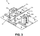
- FIG 3 is a perspective view of an R, L, C filter network according to one embodiment.
- an R, L, C network 30 may include resistors 21a, 21b, capacitor 22 and inductors 23a, 23b of Figure 1 .
- Capacitor 22 can be implemented using a pair of capacitors as shown, with each having a high impulse current rating and low series inductance.
- the minimized input inductance of R, L, C, network 30, appearing across terminals 5a and 5b of Figure 1 may be in the range 0.1 - 200 ⁇ H for example.
- Resistors 21a and 21b are low inductance resistors, and they are contained within resistor frames 31a, 31b. Each of inductors 23a and 23b may include a nano-crystalline core for high inductance in a small physical size.
- the R, L, C components are assembled onto an R, L, C assembly plate 32.
- the MOV component, labeled MOV 20 in Figure 1 is mounted separately.
- the filter network 7, including separate mountings of R, L, C assembly plate 32 and the MOV 20 component, is configured with fasteners for physical attachment to a bypass unit 9 combined with a plurality of series connected impedance injection units such as 8c, to implement the electrical configuration shown in Figure 1 .
Landscapes
- Engineering & Computer Science (AREA)
- Microelectronics & Electronic Packaging (AREA)
- Physics & Mathematics (AREA)
- Electromagnetism (AREA)
- Power Engineering (AREA)
- Emergency Protection Circuit Devices (AREA)
- Cable Transmission Systems, Equalization Of Radio And Reduction Of Echo (AREA)
Description
- Embodiments of the disclosure relate to inductor-resistor-capacitor (LRC) filters used to protect power flow control systems from disturbances traveling on a power transmission line.
- Various activities and natural events can cause disturbances on power transmission lines. These include lightning strikes, load switching, capacitive bank switching, transformer tap changes, and other utility actions. If a power flow control system operating on the transmission line is not protected, its performance may be detrimentally affected, or it may be damaged by such disturbances. There is a need in the art for protective circuits to shunt the energy associated with such a disturbance around operating circuitry of the power flow control system.
- Document
EP3518366A2 discloses a modular power flow control system for optimizing power flow control in a multi-phase power transmission system. Identical impedance injection modules are arranged in an m × n matrix, where m is the number of series-connected modules inserted into each phase (forming a leg of the installed bank of modules), and n is the number of parallel-connected legs per phase. Each impedance injection module in a phase is configurable to collectively insert a pre-determined (controllable) power control waveform into the phase to which it is attached. - Various circuits, a system and a related method are described herein for handling disturbances on power transmission lines. The circuits and method provide protection from and filtering of disturbances, for serial connected FACTS (Flexible Alternating Current Transmission System) devices.
- A first aspect of the invention, as defined in the appended
independent claim 1, specifies a power flow control system comprising a filter network, with a first terminal and a second terminal, that is insertable into a power transmission line (i.e. the filter network system is series connectable to a power transmission line). A first circuit is connected across the first terminal and the second terminal. The first circuit includes an RC (resistor and capacitor) network in parallel with a surge arrestor. The filter network is connectable to multiple IIUs (impedance injection units). A second circuit includes a first plurality of inductors and is for carrying low-frequency power. The inductors of the first plurality of inductors are connectable in series- to the first and second terminals and the IIUs. - One embodiment is a filter network that is insertable into a power transmission line. A first terminal and a second terminal are series connectable into the power transmission line. A first circuit includes a series RC (resistor and capacitor) network in parallel with a surge arrestor. A first end of the first circuit is connected to the first terminal. An opposed second end of the first circuit is connected to the second terminal. The first circuit is configured to bypass high-frequency disturbances of the power transmission line in connection with the first terminal and the second terminal. A second circuit includes a first plurality of inductors. The first plurality of inductors of the second circuit may be series connectable to a plurality of IIUs (impedance injection units). A first end of the second circuit is connected to the first terminal. An opposed second end of the second circuit is connected to the second terminal. The second circuit is to carry low-frequency power for the transmission line connectable to the first terminal and the second terminal to and from the IIUs.
- The power flow control system is adapted or configured for bypassing electrical disturbances in a power transmission line.
- A second aspect of the invention, as defined in the appended
independent claim 12, is a method of handling disturbances in a power transmission line, preferably by using a power flow control system. The method includes series connecting a first terminal and a second terminal into the power transmission line. The method includes bypassing high-frequency disturbances of the power transmission line through a first circuit that is connected across the first terminal and the second terminal. The first circuit includes a series RC (resistor and capacitor) network in parallel with a surge arrestor. The method includes carrying low-frequency power for the transmission line through the first and second terminals, through series connected inductors, to and from series connected IIUs (impedance injection units). - The described embodiments and the advantages thereof may best be understood by reference to the following description taken in conjunction with the accompanying drawings. These drawings in no way limit any changes in form and detail that may be made to the described embodiments by one skilled in the art without departing from the spirit and scope of the described embodiments.
-
Figure 1 is a schematic drawing of a filter network connected with a bypass unit and a group of impedance injection modules connected in series according to one embodiment. -
Figure 2 is a perspective view of several variations of a metal oxide varistor (MOV). -
Figure 3 is a perspective view of an R, L, C filter network according to one embodiment. - A
filter network 7 is series connectable to a power transmission line for protecting electronic equipment from high frequency disturbances on the line. A first path of the filter network causes high frequency signals to bypass the associated electronic equipment and avoid damage thereto. A high frequency signal is a signal having a frequency of 1 kHz or higher, more preferably 10 kHz or higher. A second path of the filter network passes low frequency power, up to 1 kHz in some embodiments, in a Flexible Alternating Current Transmission System (FACTS). Thefilter network 7 comprises a first circuit configured for providing the first path for bypassing high frequency signals, and a second circuit for carrying the low frequency power. Different filters may be configured for different transmission line profiles. Surge arrestors may include Metal Oxide Varistors (MOVs) and gapped and non-gapped arrestors. Using a communication link that communicates with a processor associated with the filter network an external support system may be used to determine the status of the filter network. - In a first aspect of the present invention a power flow control system includes
filter network 7 for insertion into a power transmission line to bypass electrical disturbances that may be traveling in the power transmission line. The filter network comprises a first 5a and a second 5b terminal, a first circuit and a second circuit. The first 5a and second 5b terminals are series connectable to the power transmission line. The first circuit is configured to provide a high-frequency path for bypassing high-frequency disturbances. The second circuit is configured to provide a low-frequency path for carrying power up to a frequency of 1 kHz. The first circuit of the filter network providing the high-frequency path comprises a first end connected to the first terminal, an opposed second end connected to the second terminal, and further comprises an RC network (21a, 21b, 22) connected in parallel with asurge arrestor 20. The RC network may be configured as tworespective resistors capacitor 22. The second circuit providing the low frequency path comprises a respective first end connected to the first terminal, a respective opposed second end connected to the second terminal, and further comprises a first plurality ofinductors inductors filter network 7 may be contained in a Faraday Cageenclosure 3. Thesurge arrestor 20 may be gapped or un-gapped and may include a metal oxide varistor (MOV) or a gas discharge tube or any other type of arrestor. An inductor in the low-frequency path may be a choke having a nano-crystalline core. Thus, at least one inductor (23a, 23b) of the second circuit of the filter network may be configured as a differential mode choke DMC. The input/output terminals (i.e. the first 5a and second 5b terminals) of thefilter network 7 may be spaced apart with a spacing small enough to provide low input inductance, but large enough to limit arcing and creepage between the terminals. The spacing may be predetermined to minimize a particular type of disturbance on the power transmission line. The disturbance may be associated with a particular type of grid event. The spacing may be less than two meters. Thefilter network 7 may be equipped with a communication link to an external support system. The communication link may be an RF link. The communication link may be used to communicate with a processor in thefilter network 7 to determine the status of thefilter network 7. Thefilter network 7 may be configured to bypass a high-frequency traveling wave passing through the power transmission line. The high-frequency traveling wave may be associated with a lightning strike, switching of a capacitance bank, or load switching on the power transmission line. The filter network may be configured for insertion into a serial-connected Flexible Alternating Current Transmission System (FACTS). - The power
flow control system 4 is adapted for bypassing electrical disturbances in a power transmission line. The powerflow control system 4 may preferably be configured as a Flexible Alternating Current Transmission System (FACTS). The powerflow control system 4 comprises afilter network 7 as previously described and a plurality ofIIUs 8a-8e. The plurality ofIIUs 8a-8e is preferably connected to the second circuit of thefilter network 7. The first plurality ofinductors IIUs 8a-8e. The plurality ofIIUs 8a-8e are preferably in series connection with each other. In a preferred embodiment the plurality ofIIUs 8a-8e is connected to thefirst terminal 5a through afirst subset 23a of the first plurality of inductors, and to thesecond terminal 5b through asecond subset 23b of the first plurality of inductors. - According to some compatible embodiments, the power flow control system may further comprise a bypass unit 9. The bypass unit 9 may comprise a first subsystem formed by a
further surge arrestor 16b in parallel with a silicon-controlledrectifier SCR bank 15. The first subsystem may be connected in parallel with the plurality ofIIUs 8a-8e, being subsequently series connected with the first plurality ofinductors first terminal 5a and thesecond terminal 5b. - The bypass unit 9 may further comprise a second plurality of
inductors IIUs 8a-8e. In preferred embodiments, one end of the plurality of IIUs is connected to afirst subset 13a of the second plurality of inductors, while an opposed second end of the plurality IIUs is connected to asecond subset 13b of the second plurality of inductors. The group formed by the second plurality ofinductors IIUs 8a-8e may be parallel connected to the first subsystem and subsequently series connected to the first plurality ofinductors - In some embodiments of the system, at least one IIU of the plurality of IIUs may comprise a plurality of
switches 11, acapacitor 12 and afurther surge arrestor 16a. Preferably, the respective plurality ofswitches 11 is connected as an H bridge, wherein therespective capacitor 12 is connected as a load at a crossbar of the H bridge, and wherein therespective surge arrestor 16a is arranged in parallel with the H bridge. The at least one IIU may further comprise acontroller 17a configured to control theVSL 14, directing theVSL 14 to open a switch for active use of the IIUs in power injection into the power transmission line, and close the switch to short across the series connected IIUs and deactivate the IIUs from active use. In some preferred embodiments, the powerflow control system 4 further comprises aswitch 14 connected in parallel with the plurality ofIIUs 8a-8e. Preferably, theswitch 14 is configured as a vacuum switch link VSL. In some embodiments, the group formed by theswitch 14 and the plurality ofIIUs 8a-8e is further series connected to the second plurality ofinductors - In some compatible embodiments, at least one of the
surge arrestors - In some compatible embodiments, at least one of the inductors of the first and/or the second plurality of inductors may be configured as a differential mode choke DMC.
- A second aspect of the present invention describes a method for bypassing electromagnetic disturbances traveling on a power transmission line using a filter. The method includes providing a low-pass path for passing power at frequencies up to 1 kHz and a high-pass path for bypassing high frequency disturbances. The filter may include an R, L, C network and a surge arrestor and an enclosure having the properties of a Faraday Cage. The method may include provision of a communication link for determining the status of the filter network. A processor may be provided to reside with the filter network and may perform executable instructions in a memory for communicating with an external support system. The filter network characteristics may be configured by appropriate selection of components in the R, L, C network to bypass a traveling wave threat that may be imposed by a lightning strike in a vicinity of the power transmission line, by load changes or by remote switching of a capacitance bank into the power transmission line.
-
Figure 1 illustrates a powerflow control system 4 that is series connected into a power transmission line atterminals spacing 6 between them. Powerflow control system 4 may be described as a Flexible Alternating Current Transmission System (FACTS). A power transmission line may comprise a high-voltage transmission line (e.g. 230 kV), a medium-voltage transmission line (e.g. 13.8 kV) or a distribution line (e.g. 480 V). It may reside inside or outside of a switching station. Powerflow control system 4 includes afilter network 7 of the present disclosure, a plurality ofimpedance injection units 8a-8e connected in series, and a bypass unit 9.Filter network 7 is contained within anenclosure 3.Impedance injection unit 8c includes a switchingassembly 10 comprising high-power switching devices 11, configured to inject reactive power into the power transmission line by charging and discharging aDC capacitor 12.Impedance injection unit 8c also includes a metal oxide varistor (MOV) 16a and acontroller 17a. - In one embodiment, each
impedance injection unit power switching devices 11 connected as an H bridge. Each of the high-power switching devices 11 has a bypass diode, as depicted inFigure 1 . Thecapacitor 12 is connected as a load at the crossbar of the H bridge. AnMOV 16a or other surge arrestor is connected in parallel with the H bridge. The H bridge, withappropriate switching devices 11 activated and others deactivated, can connect thecapacitor 12 in either of two opposed polarities to receive voltage and current from the transmission line andcharge capacitor 12. Then, withappropriate switching devices 11 activated and others deactivated, the H bridge can connect thecapacitor 12 in either of the two opposed polarities to inject the power from the chargedcapacitor 12 to the transmission line. In the embodiment shown inFigure 1 , these actions and states of theswitching devices 11 and the H bridge are controlled by thecontroller 17a in the IIU. - Bypass unit 9, in one embodiment, includes a second plurality of
inductors Figure 1 further comprises a vacuum switch link (VSL) 14, a bank of silicon-controlled rectifiers (SCRs) 15 and afurther surge arrestor 16b. The bank ofSCRs 15 and thefurther surge arrestor 16b are connected in parallel forming a first subsystem. Said first subsystem is respectively connected through afirst subset 13a and a second subset13b of the second plurality of inductors to the plurality ofimpedance injection units 8a-8e, and a bypass controller 17b, wherein the plurality ofimpedance injection units 8a-8e is connected in parallel with theVSL 14. Bypass controller 17b is in communication with anexternal support system 18 via acommunication link 19.Communication link 19 may be employed to have the bypass controller 17b interrogate the status offilter network 7, including a check of its I/V characteristic, in response to a command fromsupport system 18. Bypass controller 17b controls theVSL 14, directing theVSL 14 to open a switch for active use of the IIUs in power injection into the power transmission line, and close the switch to short across the series connected IIUs and deactivate the IIUs from active use.Communication link 19 may be implemented as an RF link or as a fiber optic link as examples. -
Filter network 7 may be configured to bypass or minimize traveling wave disturbances, traveling on the associated power transmission line, where the primary frequency of the traveling wave disturbance is more than 10 kHz for example, while passing power at a frequency less than 1 kHz for example. -
Filter network 7 includes asurge arrestor 20 configured as a metal oxide varistor (MOV) 20 connected acrossterminals MOV 20 has a non-linear characteristic that reacts very quickly to an overvoltage spike, such as may be caused by a lightning strike. At low frequencies, a leakage current of microamperes or nanoamperes will flow. When stressed by a voltage spike, the device may bypass kiloamperes at low impedance. In one embodiment, a specification forMOV 20 includes, as examples, a varistor voltage of 17 kV, a maximum clamping voltage of 25kV (@ 100A), a maximum peak current of 5000A, a maximum AC voltage of 7 kV, and a maximum energy dissipation of 2600J. - In some embodiments,
MOV 20 may be replaced by any type of surge arrestor. It may be gapped or gapless. A gapped arrestor will have a sharper I/V response curve. One version of a gapped arrestor is a gas discharge tube, typically used in lower power installations. Gapless arrestors typically comprise a metal oxide disk, such as described forMOV 20. Surge arrestors may be used that are described as snubbers or clamps. -
Filter network 7 may further include acapacitor 22 to provide a low-impedance path for high-frequency electrical disturbances.Capacitor 22 may have a capacitance in the range of 0.1 - 50µF for example. This path may enable resonant currents that could damage neighboring components. As shown,resistors Resistors Inductors MOV 20 or the series path ofresistor 21a,capacitor 22 andresistor 21b.Inductors filter network 7 may be referred to as a bypass characteristic, for bypassing electrical disturbances.Inductors filter network 7 is limited,inductors - The
spacing 6 of terminals betweenterminals terminals Spacing 6 may be predetermined and configured for minimizing a disturbance that corresponds to a problematic type of grid event.Spacing 6 may be less than 2 meters to cover many types of grid events or disturbances. Problematic grid events may include lighting strikes, current surges due to switching of capacitor banks, tap changes on transformers, load switching, and any other disturbance that causes a current spike on the power transmission line. These problematic grid events may be characterized by waveforms and frequencies that can be used to configure appropriate filter network configurations for bypassing them. If disturbances are effectively bypassed or minimized, thereby not requiring a utility operator or an automated safety apparatus to open a circuit breaker in the power transmission line, the operational availability of the associated powerflow control system 4 is increased, to the benefit of both power utilities and consumers. - In some embodiments,
filter network 7 is contained within anenclosure 3.Enclosure 3 may have the properties of a Faraday Cage for attenuating any disturbances such as incident waveforms from a cell tower. Waves associated with such disturbances could otherwise impinge on the enclosure and induce undesirable electromagnetic effects. The Faraday Cage ofenclosure 3 comprises a conductive material such as aluminum, where any gaps in the enclosure are small enough to block the highest frequency impinging signal, and the thickness of the enclosure is thick enough to block the lowest frequency impinging signal. -
Figure 2 is a perspective view of several variations of a metal oxide varistor (MOV). InFigure 2 , a range of transient/surge absorbers, which may be those manufactured by PANASONIC, is shown. A single-disk arrestor 25 is shown, together with a three-disk arrestor stack 26 and a six-disk arrestor stack 27. Each disk shown is a sintered zinc-oxide disk. Bigger stacks correspond with higher maximum voltages. -
Figure 3 is a perspective view of an R, L, C filter network according to one embodiment. Referring toFigure 3 , an R, L,C network 30 may includeresistors capacitor 22 andinductors Figure 1 .Capacitor 22 can be implemented using a pair of capacitors as shown, with each having a high impulse current rating and low series inductance. When the associatedimpedance injection units 8a-8e are not operational andVSL 14 is closed, the minimized input inductance of R, L, C,network 30, appearing acrossterminals Figure 1 , may be in the range 0.1 - 200 µH for example.Resistors resistor frames inductors C assembly plate 32. The MOV component, labeledMOV 20 inFigure 1 , is mounted separately. Thefilter network 7, including separate mountings of R, L,C assembly plate 32 and theMOV 20 component, is configured with fasteners for physical attachment to a bypass unit 9 combined with a plurality of series connected impedance injection units such as 8c, to implement the electrical configuration shown inFigure 1 . - The teachings contained in the embodiments described herein may be applied to many variations of power
flow control system 4, including different configurations of bypass unit 9, and different series combinations of impedance injection units such as 8c.
Claims (14)
- A power flow control system (4) insertable into a power transmission line for bypassing electrical disturbances in a power transmission line, comprising:a plurality of impedance injection units IIUs (8a-8e); anda filter network (7) comprising:
a first terminal (5a) and a second terminal (5b) that are series connectable to the power transmission line;a first circuit configured for bypassing high frequency disturbances, and comprising a first end connected to the first terminal (5a) and an opposed second end connected to the second terminal (5b), wherein the first circuit further comprises an RC network having at least one resistor (21a, 21b) series connected with at least one capacitor (22), wherein the RC network is further connected in parallel with a surge arrestor (20) and wherein the surge arrestor (20) is connected across the first terminal and the second terminal; and
a second circuit configured for carrying low frequency power, comprising a first end connected to the first terminal (5a) and an opposed second end connected to the second terminal (5b), wherein the second circuit further comprises a first plurality of inductors (23a, 23b) series-connecting the first (5a) and second (5b) terminals and the plurality of IIUs (8a-8e). - The power flow control system (4) of claim 1, wherein the plurality of IIUs (8a-8e) are in series connection with each other.
- The power flow control system (4) of claims 1 or 2, wherein the plurality of IIUs (8a-8e) is connected to the first terminal (5a) through a first subset (23a) of the first plurality of inductors (23a, 23b), and to the second terminal (5b) through a second subset (23b) of the first plurality of inductors (23a, 23b).
- The power flow control system (4) of any of the preceding claims, further comprising:a bypass unit (9) comprising a first subsystem formed by a further surge arrestor (16b) in parallel with a silicon-controlled rectifier SCR bank (15),wherein said first subsystem is connected in parallel with the plurality of IIUs (8a-8e), being subsequently series connected with the first plurality of inductors (23a, 23b) across the first terminal (5a) and the second terminal (5b).
- The power flow control system (4) of claim 4, wherein the bypass unit (9) further comprises a second plurality of inductors (13a, 13b) being series connected to the plurality of IIUs (8a-8e); wherein the second plurality of inductors (13a, 13b) and the plurality of IIUs (8a-8e) are parallel connected to the first subsystem and subsequently series connected to the first plurality of inductors (23a, 23b).
- The power flow control system (4) of any of the preceding claims, wherein at least one of the plurality of IIUs (8a-8e) comprises a plurality of switches (11), a capacitor (12), and a further surge arrestor (16a); and wherein preferably:the respective plurality of switches (11) is connected as an H bridge;the respective capacitor (12) is connected as a load at a crossbar of the H bridge; andthe respective further surge arrestor (16a) in parallel with the H bridge.
- The power flow control system (4) of any of the preceding claims, wherein at least one of the surge arrestors (16a, 16b, 20) comprises a metal oxide varistor MOV, a gapped arrestor, or a non-gapped arrestor.
- The power flow control system (4) of any of the preceding claims, further comprising a switch (14) in parallel with the plurality of IIUs (8a-8e), wherein preferably:the switch (14) is configured as a vacuum switch link VSL; and/orwherein the switch (14) and the plurality of IIU's (8a-8e) are further series connected to the second plurality of inductors (13a, 13b) of the bypass unit (9).
- The power flow control system (4) of any of the preceding claims, wherein at least one inductor of the first (23a, 23b) and/or the second (13a, 13b) plurality of inductors is configured as a differential mode choke DMC.
- The power flow control system (4) of any of the preceding claims, further comprising:
a Faraday cage enclosing at least the RC network (21a, 21b, 22) in parallel with the surge arrestor (20). - The power flow control system (4) of any of the preceding claims, further comprising at least one controller (17a, 17b):wherein preferably at least one controller (17b) is configured to check a current or voltage characteristic of the first circuit and control a switch (14) to activate and deactivate the plurality of IIUs (8a-8e); and/orwherein preferably each of the plurality of IIUs (8a-8e) has at least one further controller (17a) to control the switches (11) in the IIUs (8a-8e).
- A method of handling disturbances in a power transmission line with a power flow control system (4) according to any of the preceding claims, comprising:series connecting the first terminal (5a) and the second terminal (5b) into the power transmission line;bypassing high frequency disturbances of the power transmission line through the first circuit connected across the first terminal (5a) and the second terminal (5b), the first circuit comprising a series RC (21a, 21b, 22) network in parallel with a surge arrestor (20); andcarrying low-frequency power for the power transmission line through the first (5a) and second terminals (5b), through a plurality of series connected inductors (23a, 23b), to and from a plurality of series connected impedance injection units IIUs (8a-8e).
- The method of claim 12, further comprising:
further bypassing at least a portion of the high frequency disturbances of the power transmission line through the bypass unit (9). - The method of claims 12 or 13, further comprising:
operating, through one or more controllers (17a, 17b), a plurality of switches (11) to activate and deactivate the plurality of series connected IIUs (8a-8e) and for the carrying of low-frequency power to and from one or more capacitors (12) in the plurality of series connected IIUs (8a-8e).
Applications Claiming Priority (2)
| Application Number | Priority Date | Filing Date | Title |
|---|---|---|---|
| US202063047154P | 2020-07-01 | 2020-07-01 | |
| US17/197,627 US11469015B2 (en) | 2020-07-01 | 2021-03-10 | Protection from and filtering of disturbances for serial connected facts |
Publications (3)
| Publication Number | Publication Date |
|---|---|
| EP3934041A2 EP3934041A2 (en) | 2022-01-05 |
| EP3934041A3 EP3934041A3 (en) | 2022-01-19 |
| EP3934041B1 true EP3934041B1 (en) | 2022-06-08 |
Family
ID=76522878
Family Applications (1)
| Application Number | Title | Priority Date | Filing Date |
|---|---|---|---|
| EP21180237.6A Active EP3934041B1 (en) | 2020-07-01 | 2021-06-18 | Protection from and filtering of disturbances for serial connected facts |
Country Status (3)
| Country | Link |
|---|---|
| US (1) | US11469015B2 (en) |
| EP (1) | EP3934041B1 (en) |
| AU (1) | AU2021204305A1 (en) |
Families Citing this family (2)
| Publication number | Priority date | Publication date | Assignee | Title |
|---|---|---|---|---|
| US11095369B2 (en) * | 2019-03-07 | 2021-08-17 | Arris Enterprises Llc | Device and method for launching tranverse magnetic waves |
| US12255549B1 (en) * | 2020-10-21 | 2025-03-18 | Smart Wires Inc. | High current Voltage-Source Converter |
Family Cites Families (17)
| Publication number | Priority date | Publication date | Assignee | Title |
|---|---|---|---|---|
| GB1122901A (en) | 1966-05-11 | 1968-08-07 | Pilkington Brothers Ltd | Improvements in or relating to the handling of tubular members made, for example, ofglass |
| US3956743A (en) | 1973-03-14 | 1976-05-11 | Theodore D. Geiszler | Motion detection system |
| US4123748A (en) | 1976-12-08 | 1978-10-31 | Nippon Prosensor Co., Ltd. | Burglar alarms utilizing ultrasonic waves |
| US4376968A (en) | 1981-02-13 | 1983-03-15 | Borg-Warner Corporation | Protection system for immunizing an inverter system against A-C line voltage disturbances |
| US4459629A (en) * | 1981-11-23 | 1984-07-10 | General Electric Company | Electric circuit breaker utilizing semiconductor diodes for facilitating interruption |
| US4682369A (en) | 1985-03-04 | 1987-07-21 | Texas Instruments Incorporated | Ripple and droop reduction circuit |
| US5581256A (en) | 1994-09-06 | 1996-12-03 | The Regents Of The University Of California | Range gated strip proximity sensor |
| JP3358381B2 (en) | 1995-04-24 | 2002-12-16 | 日産自動車株式会社 | Control device for continuously variable automatic transmission |
| US6194881B1 (en) | 1999-05-17 | 2001-02-27 | Nmb (Usa), Inc | Switching power supply for lowered distribution system disturbance |
| US6417791B1 (en) | 2001-06-25 | 2002-07-09 | Schweitzer Engineering Laboratories, Inc. | Delta filter with an adaptive time window for protective relays |
| US7031558B2 (en) | 2003-08-18 | 2006-04-18 | Hassan Tanbakuchi | Low-pass filter transmission line with integral electroabsorption modulator |
| DE102009002009A1 (en) | 2009-03-31 | 2010-10-07 | Endress + Hauser Gmbh + Co. Kg | Device for reducing or minimizing interference signals in a field device of process automation |
| WO2013174429A1 (en) * | 2012-05-23 | 2013-11-28 | Abb Technology Ltd | An apparatus for assisting or controlling the electric power transmission in a dc power transmission system |
| JP6607313B2 (en) | 2016-06-08 | 2019-11-20 | 日産自動車株式会社 | Control method for hybrid vehicle and control device for hybrid vehicle |
| CN206765820U (en) * | 2017-03-31 | 2017-12-19 | 苏州汇川联合动力系统有限公司 | A kind of filter circuit and new energy electric motor vehicle electric-control system |
| US10756542B2 (en) * | 2018-01-26 | 2020-08-25 | Smart Wires Inc. | Agile deployment of optimized power flow control system on the grid |
| US11070045B1 (en) * | 2020-06-15 | 2021-07-20 | Hong Kong Applied Science and Technology Research Institute Company Limited | Electrical protective device for low-voltage direct current (LVDC) network |
-
2021
- 2021-03-10 US US17/197,627 patent/US11469015B2/en active Active
- 2021-06-18 EP EP21180237.6A patent/EP3934041B1/en active Active
- 2021-06-24 AU AU2021204305A patent/AU2021204305A1/en active Pending
Also Published As
| Publication number | Publication date |
|---|---|
| US11469015B2 (en) | 2022-10-11 |
| EP3934041A3 (en) | 2022-01-19 |
| US20220005633A1 (en) | 2022-01-06 |
| EP3934041A2 (en) | 2022-01-05 |
| AU2021204305A1 (en) | 2022-01-20 |
Similar Documents
| Publication | Publication Date | Title |
|---|---|---|
| US11309701B2 (en) | Modular FACTS devices with external fault current protection | |
| CA2311137C (en) | A surge suppression network responsive to the rate of change of power disturbances | |
| KR101948455B1 (en) | System for protection of dry type transformers | |
| EP2577701B1 (en) | A very fast transient suppressing device | |
| US20100123356A1 (en) | Resonance mitigation system and method | |
| CN110676827B (en) | Power electronic device | |
| US11469015B2 (en) | Protection from and filtering of disturbances for serial connected facts | |
| US10998718B2 (en) | Lightning and overvoltage protection device for data networks, telephony services, electroacoustic installations or bus systems | |
| KR101544573B1 (en) | Surge protector system | |
| Xu et al. | Lightning impulse protection for grid-connected solid-state transformers | |
| WO2008025424A1 (en) | A device for suppressing high frequency current or/and voltage components | |
| WO2018080645A1 (en) | Fault current limiter with modular mutual reactor | |
| US11824350B1 (en) | Clamping circuit for protecting FACTs | |
| US7446436B2 (en) | Waveform correction filters | |
| KR20190113318A (en) | Surge protect device of three phase power with four lines capable of powerline communications | |
| EP2287990A1 (en) | A device protecting against high frequency overvoltage | |
| Pilvelait et al. | Advanced series compensation for transmission systems using a switched capacitor module | |
| CN111064165A (en) | Protection circuit, frequency converter device and electrical equipment | |
| CN107241084A (en) | A kind of wide heavy current pulse power source device of long pulse of the equal current transformer of band | |
| CN223599506U (en) | Surge protection circuits and surge protectors | |
| EP4645623A1 (en) | Circuit breaker with a passive clamping circuit including capacitors, operation method, dc network and aircraft | |
| Das | Effects of medium voltage capacitor bank switching surges in an industrial distribution system | |
| US20250087995A1 (en) | Wide input voltage range surge suppressor | |
| CN2433760Y (en) | Thunder-lightning-proof overtension combination protection equipment | |
| CA1153096A (en) | Commutation circuit for an hvdc circuit breaker |
Legal Events
| Date | Code | Title | Description |
|---|---|---|---|
| PUAI | Public reference made under article 153(3) epc to a published international application that has entered the european phase |
Free format text: ORIGINAL CODE: 0009012 |
|
| STAA | Information on the status of an ep patent application or granted ep patent |
Free format text: STATUS: THE APPLICATION HAS BEEN PUBLISHED |
|
| PUAL | Search report despatched |
Free format text: ORIGINAL CODE: 0009013 |
|
| AK | Designated contracting states |
Kind code of ref document: A2 Designated state(s): AL AT BE BG CH CY CZ DE DK EE ES FI FR GB GR HR HU IE IS IT LI LT LU LV MC MK MT NL NO PL PT RO RS SE SI SK SM TR |
|
| AK | Designated contracting states |
Kind code of ref document: A3 Designated state(s): AL AT BE BG CH CY CZ DE DK EE ES FI FR GB GR HR HU IE IS IT LI LT LU LV MC MK MT NL NO PL PT RO RS SE SI SK SM TR |
|
| RIC1 | Information provided on ipc code assigned before grant |
Ipc: H02H 9/02 20060101ALI20211214BHEP Ipc: H02H 9/00 20060101AFI20211214BHEP |
|
| STAA | Information on the status of an ep patent application or granted ep patent |
Free format text: STATUS: REQUEST FOR EXAMINATION WAS MADE |
|
| 17P | Request for examination filed |
Effective date: 20220125 |
|
| RBV | Designated contracting states (corrected) |
Designated state(s): AL AT BE BG CH CY CZ DE DK EE ES FI FR GB GR HR HU IE IS IT LI LT LU LV MC MK MT NL NO PL PT RO RS SE SI SK SM TR |
|
| GRAP | Despatch of communication of intention to grant a patent |
Free format text: ORIGINAL CODE: EPIDOSNIGR1 |
|
| STAA | Information on the status of an ep patent application or granted ep patent |
Free format text: STATUS: GRANT OF PATENT IS INTENDED |
|
| INTG | Intention to grant announced |
Effective date: 20220329 |
|
| GRAS | Grant fee paid |
Free format text: ORIGINAL CODE: EPIDOSNIGR3 |
|
| GRAA | (expected) grant |
Free format text: ORIGINAL CODE: 0009210 |
|
| STAA | Information on the status of an ep patent application or granted ep patent |
Free format text: STATUS: THE PATENT HAS BEEN GRANTED |
|
| AK | Designated contracting states |
Kind code of ref document: B1 Designated state(s): AL AT BE BG CH CY CZ DE DK EE ES FI FR GB GR HR HU IE IS IT LI LT LU LV MC MK MT NL NO PL PT RO RS SE SI SK SM TR |
|
| REG | Reference to a national code |
Ref country code: AT Ref legal event code: REF Ref document number: 1497579 Country of ref document: AT Kind code of ref document: T Effective date: 20220615 Ref country code: CH Ref legal event code: EP |
|
| REG | Reference to a national code |
Ref country code: DE Ref legal event code: R096 Ref document number: 602021000133 Country of ref document: DE |
|
| REG | Reference to a national code |
Ref country code: IE Ref legal event code: FG4D |
|
| REG | Reference to a national code |
Ref country code: LT Ref legal event code: MG9D |
|
| REG | Reference to a national code |
Ref country code: NL Ref legal event code: MP Effective date: 20220608 |
|
| PG25 | Lapsed in a contracting state [announced via postgrant information from national office to epo] |
Ref country code: SE Free format text: LAPSE BECAUSE OF FAILURE TO SUBMIT A TRANSLATION OF THE DESCRIPTION OR TO PAY THE FEE WITHIN THE PRESCRIBED TIME-LIMIT Effective date: 20220608 Ref country code: NO Free format text: LAPSE BECAUSE OF FAILURE TO SUBMIT A TRANSLATION OF THE DESCRIPTION OR TO PAY THE FEE WITHIN THE PRESCRIBED TIME-LIMIT Effective date: 20220908 Ref country code: LT Free format text: LAPSE BECAUSE OF FAILURE TO SUBMIT A TRANSLATION OF THE DESCRIPTION OR TO PAY THE FEE WITHIN THE PRESCRIBED TIME-LIMIT Effective date: 20220608 Ref country code: HR Free format text: LAPSE BECAUSE OF FAILURE TO SUBMIT A TRANSLATION OF THE DESCRIPTION OR TO PAY THE FEE WITHIN THE PRESCRIBED TIME-LIMIT Effective date: 20220608 Ref country code: GR Free format text: LAPSE BECAUSE OF FAILURE TO SUBMIT A TRANSLATION OF THE DESCRIPTION OR TO PAY THE FEE WITHIN THE PRESCRIBED TIME-LIMIT Effective date: 20220909 Ref country code: FI Free format text: LAPSE BECAUSE OF FAILURE TO SUBMIT A TRANSLATION OF THE DESCRIPTION OR TO PAY THE FEE WITHIN THE PRESCRIBED TIME-LIMIT Effective date: 20220608 Ref country code: BG Free format text: LAPSE BECAUSE OF FAILURE TO SUBMIT A TRANSLATION OF THE DESCRIPTION OR TO PAY THE FEE WITHIN THE PRESCRIBED TIME-LIMIT Effective date: 20220908 |
|
| REG | Reference to a national code |
Ref country code: AT Ref legal event code: MK05 Ref document number: 1497579 Country of ref document: AT Kind code of ref document: T Effective date: 20220608 |
|
| PG25 | Lapsed in a contracting state [announced via postgrant information from national office to epo] |
Ref country code: RS Free format text: LAPSE BECAUSE OF FAILURE TO SUBMIT A TRANSLATION OF THE DESCRIPTION OR TO PAY THE FEE WITHIN THE PRESCRIBED TIME-LIMIT Effective date: 20220608 Ref country code: LV Free format text: LAPSE BECAUSE OF FAILURE TO SUBMIT A TRANSLATION OF THE DESCRIPTION OR TO PAY THE FEE WITHIN THE PRESCRIBED TIME-LIMIT Effective date: 20220608 |
|
| PG25 | Lapsed in a contracting state [announced via postgrant information from national office to epo] |
Ref country code: NL Free format text: LAPSE BECAUSE OF FAILURE TO SUBMIT A TRANSLATION OF THE DESCRIPTION OR TO PAY THE FEE WITHIN THE PRESCRIBED TIME-LIMIT Effective date: 20220608 |
|
| PG25 | Lapsed in a contracting state [announced via postgrant information from national office to epo] |
Ref country code: SM Free format text: LAPSE BECAUSE OF FAILURE TO SUBMIT A TRANSLATION OF THE DESCRIPTION OR TO PAY THE FEE WITHIN THE PRESCRIBED TIME-LIMIT Effective date: 20220608 Ref country code: SK Free format text: LAPSE BECAUSE OF FAILURE TO SUBMIT A TRANSLATION OF THE DESCRIPTION OR TO PAY THE FEE WITHIN THE PRESCRIBED TIME-LIMIT Effective date: 20220608 Ref country code: RO Free format text: LAPSE BECAUSE OF FAILURE TO SUBMIT A TRANSLATION OF THE DESCRIPTION OR TO PAY THE FEE WITHIN THE PRESCRIBED TIME-LIMIT Effective date: 20220608 Ref country code: PT Free format text: LAPSE BECAUSE OF FAILURE TO SUBMIT A TRANSLATION OF THE DESCRIPTION OR TO PAY THE FEE WITHIN THE PRESCRIBED TIME-LIMIT Effective date: 20221010 Ref country code: ES Free format text: LAPSE BECAUSE OF FAILURE TO SUBMIT A TRANSLATION OF THE DESCRIPTION OR TO PAY THE FEE WITHIN THE PRESCRIBED TIME-LIMIT Effective date: 20220608 Ref country code: EE Free format text: LAPSE BECAUSE OF FAILURE TO SUBMIT A TRANSLATION OF THE DESCRIPTION OR TO PAY THE FEE WITHIN THE PRESCRIBED TIME-LIMIT Effective date: 20220608 Ref country code: CZ Free format text: LAPSE BECAUSE OF FAILURE TO SUBMIT A TRANSLATION OF THE DESCRIPTION OR TO PAY THE FEE WITHIN THE PRESCRIBED TIME-LIMIT Effective date: 20220608 Ref country code: AT Free format text: LAPSE BECAUSE OF FAILURE TO SUBMIT A TRANSLATION OF THE DESCRIPTION OR TO PAY THE FEE WITHIN THE PRESCRIBED TIME-LIMIT Effective date: 20220608 |
|
| PG25 | Lapsed in a contracting state [announced via postgrant information from national office to epo] |
Ref country code: PL Free format text: LAPSE BECAUSE OF FAILURE TO SUBMIT A TRANSLATION OF THE DESCRIPTION OR TO PAY THE FEE WITHIN THE PRESCRIBED TIME-LIMIT Effective date: 20220608 Ref country code: IS Free format text: LAPSE BECAUSE OF FAILURE TO SUBMIT A TRANSLATION OF THE DESCRIPTION OR TO PAY THE FEE WITHIN THE PRESCRIBED TIME-LIMIT Effective date: 20221008 |
|
| REG | Reference to a national code |
Ref country code: DE Ref legal event code: R097 Ref document number: 602021000133 Country of ref document: DE |
|
| PG25 | Lapsed in a contracting state [announced via postgrant information from national office to epo] |
Ref country code: MC Free format text: LAPSE BECAUSE OF FAILURE TO SUBMIT A TRANSLATION OF THE DESCRIPTION OR TO PAY THE FEE WITHIN THE PRESCRIBED TIME-LIMIT Effective date: 20220608 Ref country code: AL Free format text: LAPSE BECAUSE OF FAILURE TO SUBMIT A TRANSLATION OF THE DESCRIPTION OR TO PAY THE FEE WITHIN THE PRESCRIBED TIME-LIMIT Effective date: 20220608 |
|
| PLBE | No opposition filed within time limit |
Free format text: ORIGINAL CODE: 0009261 |
|
| STAA | Information on the status of an ep patent application or granted ep patent |
Free format text: STATUS: NO OPPOSITION FILED WITHIN TIME LIMIT |
|
| PG25 | Lapsed in a contracting state [announced via postgrant information from national office to epo] |
Ref country code: DK Free format text: LAPSE BECAUSE OF FAILURE TO SUBMIT A TRANSLATION OF THE DESCRIPTION OR TO PAY THE FEE WITHIN THE PRESCRIBED TIME-LIMIT Effective date: 20220608 |
|
| 26N | No opposition filed |
Effective date: 20230310 |
|
| P01 | Opt-out of the competence of the unified patent court (upc) registered |
Effective date: 20230511 |
|
| PG25 | Lapsed in a contracting state [announced via postgrant information from national office to epo] |
Ref country code: FR Free format text: LAPSE BECAUSE OF NON-PAYMENT OF DUE FEES Effective date: 20220808 |
|
| PG25 | Lapsed in a contracting state [announced via postgrant information from national office to epo] |
Ref country code: IT Free format text: LAPSE BECAUSE OF FAILURE TO SUBMIT A TRANSLATION OF THE DESCRIPTION OR TO PAY THE FEE WITHIN THE PRESCRIBED TIME-LIMIT Effective date: 20220608 |
|
| REG | Reference to a national code |
Ref country code: BE Ref legal event code: MM Effective date: 20230630 |
|
| PG25 | Lapsed in a contracting state [announced via postgrant information from national office to epo] |
Ref country code: LU Free format text: LAPSE BECAUSE OF NON-PAYMENT OF DUE FEES Effective date: 20230618 |
|
| PG25 | Lapsed in a contracting state [announced via postgrant information from national office to epo] |
Ref country code: LU Free format text: LAPSE BECAUSE OF NON-PAYMENT OF DUE FEES Effective date: 20230618 |
|
| PG25 | Lapsed in a contracting state [announced via postgrant information from national office to epo] |
Ref country code: BE Free format text: LAPSE BECAUSE OF NON-PAYMENT OF DUE FEES Effective date: 20230630 |
|
| PG25 | Lapsed in a contracting state [announced via postgrant information from national office to epo] |
Ref country code: TR Free format text: LAPSE BECAUSE OF FAILURE TO SUBMIT A TRANSLATION OF THE DESCRIPTION OR TO PAY THE FEE WITHIN THE PRESCRIBED TIME-LIMIT Effective date: 20220608 |
|
| PG25 | Lapsed in a contracting state [announced via postgrant information from national office to epo] |
Ref country code: BG Free format text: LAPSE BECAUSE OF FAILURE TO SUBMIT A TRANSLATION OF THE DESCRIPTION OR TO PAY THE FEE WITHIN THE PRESCRIBED TIME-LIMIT Effective date: 20220608 |
|
| PG25 | Lapsed in a contracting state [announced via postgrant information from national office to epo] |
Ref country code: BG Free format text: LAPSE BECAUSE OF FAILURE TO SUBMIT A TRANSLATION OF THE DESCRIPTION OR TO PAY THE FEE WITHIN THE PRESCRIBED TIME-LIMIT Effective date: 20220608 |
|
| REG | Reference to a national code |
Ref country code: CH Ref legal event code: PL |
|
| PG25 | Lapsed in a contracting state [announced via postgrant information from national office to epo] |
Ref country code: CH Free format text: LAPSE BECAUSE OF NON-PAYMENT OF DUE FEES Effective date: 20240630 |
|
| PGFP | Annual fee paid to national office [announced via postgrant information from national office to epo] |
Ref country code: DE Payment date: 20250618 Year of fee payment: 5 |
|
| PGFP | Annual fee paid to national office [announced via postgrant information from national office to epo] |
Ref country code: GB Payment date: 20250618 Year of fee payment: 5 |
|
| PG25 | Lapsed in a contracting state [announced via postgrant information from national office to epo] |
Ref country code: CY Free format text: LAPSE BECAUSE OF FAILURE TO SUBMIT A TRANSLATION OF THE DESCRIPTION OR TO PAY THE FEE WITHIN THE PRESCRIBED TIME-LIMIT; INVALID AB INITIO Effective date: 20210618 |
|
| PGFP | Annual fee paid to national office [announced via postgrant information from national office to epo] |
Ref country code: IE Payment date: 20250618 Year of fee payment: 5 |
|
| PG25 | Lapsed in a contracting state [announced via postgrant information from national office to epo] |
Ref country code: HU Free format text: LAPSE BECAUSE OF FAILURE TO SUBMIT A TRANSLATION OF THE DESCRIPTION OR TO PAY THE FEE WITHIN THE PRESCRIBED TIME-LIMIT; INVALID AB INITIO Effective date: 20210618 |
|
| PG25 | Lapsed in a contracting state [announced via postgrant information from national office to epo] |
Ref country code: SI Free format text: LAPSE BECAUSE OF FAILURE TO SUBMIT A TRANSLATION OF THE DESCRIPTION OR TO PAY THE FEE WITHIN THE PRESCRIBED TIME-LIMIT Effective date: 20220608 |