EP3933894A1 - Memory and forming method therefor - Google Patents
Memory and forming method therefor Download PDFInfo
- Publication number
- EP3933894A1 EP3933894A1 EP20885826.6A EP20885826A EP3933894A1 EP 3933894 A1 EP3933894 A1 EP 3933894A1 EP 20885826 A EP20885826 A EP 20885826A EP 3933894 A1 EP3933894 A1 EP 3933894A1
- Authority
- EP
- European Patent Office
- Prior art keywords
- patterns
- peripheral
- substrate
- active areas
- area
- Prior art date
- Legal status (The legal status is an assumption and is not a legal conclusion. Google has not performed a legal analysis and makes no representation as to the accuracy of the status listed.)
- Pending
Links
Images




Classifications
-
- H—ELECTRICITY
- H10—SEMICONDUCTOR DEVICES; ELECTRIC SOLID-STATE DEVICES NOT OTHERWISE PROVIDED FOR
- H10P—GENERIC PROCESSES OR APPARATUS FOR THE MANUFACTURE OR TREATMENT OF DEVICES COVERED BY CLASS H10
- H10P50/00—Etching of wafers, substrates or parts of devices
- H10P50/69—Etching of wafers, substrates or parts of devices using masks for semiconductor materials
- H10P50/691—Etching of wafers, substrates or parts of devices using masks for semiconductor materials for Group V materials or Group III-V materials
- H10P50/692—Etching of wafers, substrates or parts of devices using masks for semiconductor materials for Group V materials or Group III-V materials characterised by their composition, e.g. multilayer masks or materials
-
- H—ELECTRICITY
- H10—SEMICONDUCTOR DEVICES; ELECTRIC SOLID-STATE DEVICES NOT OTHERWISE PROVIDED FOR
- H10P—GENERIC PROCESSES OR APPARATUS FOR THE MANUFACTURE OR TREATMENT OF DEVICES COVERED BY CLASS H10
- H10P50/00—Etching of wafers, substrates or parts of devices
- H10P50/69—Etching of wafers, substrates or parts of devices using masks for semiconductor materials
- H10P50/691—Etching of wafers, substrates or parts of devices using masks for semiconductor materials for Group V materials or Group III-V materials
- H10P50/693—Etching of wafers, substrates or parts of devices using masks for semiconductor materials for Group V materials or Group III-V materials characterised by their size, orientation, disposition, behaviour or shape, in horizontal or vertical plane
- H10P50/695—Etching of wafers, substrates or parts of devices using masks for semiconductor materials for Group V materials or Group III-V materials characterised by their size, orientation, disposition, behaviour or shape, in horizontal or vertical plane characterised by the process involved to create the mask, e.g. lift-off masks or sidewalls or to modify the mask
-
- H—ELECTRICITY
- H10—SEMICONDUCTOR DEVICES; ELECTRIC SOLID-STATE DEVICES NOT OTHERWISE PROVIDED FOR
- H10W—GENERIC PACKAGES, INTERCONNECTIONS, CONNECTORS OR OTHER CONSTRUCTIONAL DETAILS OF DEVICES COVERED BY CLASS H10
- H10W10/00—Isolation regions in semiconductor bodies between components of integrated devices
- H10W10/01—Manufacture or treatment
- H10W10/011—Manufacture or treatment of isolation regions comprising dielectric materials
- H10W10/014—Manufacture or treatment of isolation regions comprising dielectric materials using trench refilling with dielectric materials, e.g. shallow trench isolations
-
- H—ELECTRICITY
- H10—SEMICONDUCTOR DEVICES; ELECTRIC SOLID-STATE DEVICES NOT OTHERWISE PROVIDED FOR
- H10B—ELECTRONIC MEMORY DEVICES
- H10B12/00—Dynamic random access memory [DRAM] devices
- H10B12/01—Manufacture or treatment
- H10B12/09—Manufacture or treatment with simultaneous manufacture of the peripheral circuit region and memory cells
-
- H—ELECTRICITY
- H10—SEMICONDUCTOR DEVICES; ELECTRIC SOLID-STATE DEVICES NOT OTHERWISE PROVIDED FOR
- H10P—GENERIC PROCESSES OR APPARATUS FOR THE MANUFACTURE OR TREATMENT OF DEVICES COVERED BY CLASS H10
- H10P50/00—Etching of wafers, substrates or parts of devices
- H10P50/69—Etching of wafers, substrates or parts of devices using masks for semiconductor materials
- H10P50/691—Etching of wafers, substrates or parts of devices using masks for semiconductor materials for Group V materials or Group III-V materials
- H10P50/693—Etching of wafers, substrates or parts of devices using masks for semiconductor materials for Group V materials or Group III-V materials characterised by their size, orientation, disposition, behaviour or shape, in horizontal or vertical plane
-
- H—ELECTRICITY
- H10—SEMICONDUCTOR DEVICES; ELECTRIC SOLID-STATE DEVICES NOT OTHERWISE PROVIDED FOR
- H10W—GENERIC PACKAGES, INTERCONNECTIONS, CONNECTORS OR OTHER CONSTRUCTIONAL DETAILS OF DEVICES COVERED BY CLASS H10
- H10W10/00—Isolation regions in semiconductor bodies between components of integrated devices
- H10W10/10—Isolation regions comprising dielectric materials
- H10W10/17—Isolation regions comprising dielectric materials formed using trench refilling with dielectric materials, e.g. shallow trench isolations
-
- H—ELECTRICITY
- H10—SEMICONDUCTOR DEVICES; ELECTRIC SOLID-STATE DEVICES NOT OTHERWISE PROVIDED FOR
- H10B—ELECTRONIC MEMORY DEVICES
- H10B12/00—Dynamic random access memory [DRAM] devices
- H10B12/30—DRAM devices comprising one-transistor - one-capacitor [1T-1C] memory cells
- H10B12/48—Data lines or contacts therefor
- H10B12/488—Word lines
Definitions
- the present disclosure relates to the field of memory technologies, and more particularly, to a memory and a formation method thereof.
- a memory includes a plurality of memory cells arranged in an array, and each of the memory cells is formed on an active area (AA).
- AA active area
- a memory capacity of the memory increases, a memory density increases, and a line width of the active area gradually shrinks.
- SADP self-aligned double patterning
- STI shallow trench isolation
- a size of the formed active area is very small because the size of the AA mask is small, and thus an edge of an active area array may have problems such as collapse and stress, which may have a negative effect on product yield.
- a technical problem to be solved by the present disclosure is to provide a memory and a formation method thereof which can improve an edge problem of an active area array of a memory.
- the present disclosure provides a formation method of a memory.
- the method includes: providing a substrate including an array area; forming a first mask layer on a surface of the substrate, wherein a plurality of strip-shaped patterns arranged in parallel are formed in the first mask layer to form, in the array area of the substrate, a plurality of strip-shaped continuous active areas arranged in parallel; forming a second mask layer on the first mask layer, wherein a plurality of first patterns and a plurality of second patterns are formed in the second mask layer, the plurality of first patterns are arranged in an array and are overlapped with the strip-shaped patterns to form division trenches in the substrate to divide the continuous active areas into a plurality of separate discrete active areas arranged in an array, wherein the plurality of second patterns cover ends of a part of the strip-shaped patterns to remove secondary active areas positioned at ends of a part of continuous active areas, wherein the secondary active areas are formed after the continuous active areas are divided by the first patterns and are less than the discrete active areas in
- the strip-shaped patterns are formed by using an SADP method.
- the plurality of first patterns include central first patterns and peripheral first patterns, wherein the peripheral first patterns are outermost first pattern, and the central first patterns are positioned at an inner side of the peripheral first pattern.
- the peripheral first pattern extends outward along a length direction of the strip-shaped pattern, such that a size of the peripheral first pattern is greater than that of the central first pattern.
- a size of an outermost division trench is greater than sizes of division trenches in other positions.
- the substrate further includes a peripheral area encircling the array area, and in the second mask layer there is further formed a third pattern positioned on the peripheral area of the substrate and encircling all the strip-shaped patterns.
- the third pattern is configured for forming, in the peripheral area of the substrate, a peripheral trench encircling the array area.
- a sidewall of the peripheral trench facing toward a side of the array area is a curved surface.
- the formation method further includes: filling an insulating material in the division trench and the peripheral trench to form a shallow trench isolation structure.
- the technical solution of the present disclosure also provides a memory, including a substrate, the substrate including an array area.
- a plurality of discrete active areas arranged in an array are formed in the array area.
- the discrete active areas are isolated by the shallow trench isolation structure, wherein sizes of at least a part of the outermost shallow trench isolation structures in a length direction of the discrete active area are greater than those of shallow trench isolation structures in other positions in the length direction of the discrete active area.
- the substrate further includes a peripheral area encircling the array area, a peripheral shallow trench isolation structure is formed in the peripheral area of the substrate, and the peripheral shallow trench isolation structure encircles the array area.
- the discrete active area is isolated from the peripheral area by the shallow trench isolation structure.
- a sidewall of the peripheral shallow trench isolation structure facing toward a side of the array area is a curved surface.
- peripheral shallow trench isolation structure there is a certain spacing between the peripheral shallow trench isolation structure and the array area.
- the size of the outermost shallow trench isolation structure is greater than those of the shallow trench isolation structures in other positions.
- the smaller-sized secondary active area at the edge of the discrete active area array is removed. Therefore, problems such as collapse due to the smaller-sized secondary active area present at the edge of the active area array may be prevented, and thus the reliability of the memory can be improved.
- a peripheral shallow trench isolation structure for dividing the continuous active area has a larger size, which can avoid an etching load effect in the process of forming a trench by etching. Therefore, a photoetching process window is reduced, and a patterning accuracy in the formation of the shallow trench isolation structure is enhanced, and thus performance of the memory is further improved.
- FIG. 1 to FIG. 8 are schematic structural diagrams showing formation processes of a memory according to some embodiments.
- FIG. 1 a schematic structural diagram showing formation processes of the memory according to an embodiment of the present disclosure is illustrated.
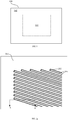
- the substrate 100 includes an array area 101 and a peripheral area 102 encircling the array area 101.
- the array area 101 there is an active area array for forming a memory
- a peripheral device such as a logic control circuit
- a first mask layer 200 is formed on a surface of the substrate 100.
- a plurality of strip-shaped patterns 201 arranged in parallel are formed in the first mask layer 200 and include a strip-shaped pattern 201a and a strip-shaped pattern 201b.
- the strip-shaped patterns 201 are covered patterns and are configured for forming, in the array area 101 of the substrate 100, a plurality of discrete and strip-shaped continuous active areas arranged in parallel. Between the strip-shaped patterns 201 there is an opening 202, configured for separating the strip-shaped patterns 201.
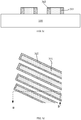
- FIG. 2a is a schematic top view
- FIG. 2b is a schematic cross-sectional view along a secant line AA' in FIG. 2a .
- a buffer layer, a hard mask layer or the like may also be formed on the surface of the substrate 100 to improve the pattern-transfer accuracy in subsequent etching processes.
- the strip-shaped pattern is formed by the SADP method.
- FIG. 3a to FIG. 3f schematic structural diagrams showing a method for forming the first mask layer according to an embodiment of the present disclosure are illustrated.
- FIG. 3a is a schematic top view of the mask pattern 301
- FIG. 3b is a schematic cross-sectional view along the secant line BB' in FIG. 3a .
- the mask pattern 301 has strip-shaped patterns arranged in parallel.
- the mask pattern 301 is arranged obliquely to increase an arrangement density of the discrete active areas formed subsequently.
- the mask pattern 301 may also be arranged horizontally or vertically.
- a sidewall 302 is formed on a sidewall of the mask pattern 301, and the sidewall 302 encircles the sidewall of the mask pattern 301.
- a first mask material 310 is filled and formed on the surface of the substrate 100, and a surface of the first mask material 310 is flush with a surface of the mask pattern 301.
- the sidewall 302 is removed to form an opening 303 (corresponding to the opening 202 in FIG. 2 ).
- the mask pattern 301 (corresponding to the strip-shaped pattern 201a in FIG. 2 ) and a mask pattern 311 (corresponding to the strip-shaped pattern 202b in FIG. 2 ) on two sides of the opening are used as strip-shaped patterns to define a width and a length of the continuous active area to be formed in the substrate subsequently.
- a spacing between adjacent strip-shaped patterns may be reduced, such that a density of the strip-shaped patterns can be increased.
- a second mask layer 400 is formed on the first mask layer 200, a plurality of first patterns 401 and a plurality of second patterns 402 are formed in the second mask layer 400.
- the plurality of first patterns 401 are arranged in an array and are overlapped with the strip-shaped patterns 201a and 201b to form division trenches in the substrate 100 so that the continuous active areas are divided into a plurality of discrete active areas arranged in an array.
- the plurality of second patterns 402 cover ends of a part of the strip-shaped pattern 201a to remove secondary active areas positioned at ends of a part of continuous active areas, wherein the secondary active areas are formed after the continuous active areas are divided by the first patterns 401 and are less than the discrete active areas in length.
- FIG. 4a only the first patterns 401 and the second patterns 402 in the second mask layer 400 are shown.
- the first patterns 401 and the second patterns 402 are both opening patterns, and the other areas are covered patterns (not shown in the figure).
- FIG. 4b is a schematic cross-sectional view along a secant line AA' in FIG. 4a .
- a filling layer 410 that fills up the opening 202 in the first mask layer 200 and has a planar surface, and the second mask layer 400 is formed on the planar surface of the filling layer 410.
- a material of the filling layer 410 may be an organic anti-reflection layer, silicon oxide or the like.
- the first pattern 401 is an opening pattern, and the strip-shaped patterns 201a and 201b are covered patterns. Therefore, after the substrate 100 is etched along the first pattern 401, a division trench is formed by cutting off the continuous active area correspondingly formed by the strip-shaped patterns 201a and 201b in the substrate 100.
- the first patterns 401 are arranged in staggered rows, such that the discrete active areas formed after division are arranged in staggered rows to increase the number of discrete active areas. This may cause the active areas positioned at ends to be less than the normal discrete active areas in length after a part of continuous active areas are divided, and these active areas with shorter length are referred to as secondary active areas.
- the secondary active area is unable to form a complete memory cell, and is prone to problems such as collapse.
- a formation position of the secondary active area generally corresponds to an end of the strip-shaped pattern 201a encircled by the opening 202.
- a second pattern 402 which is also an opening pattern.
- an end of the strip-shaped pattern 201b at an outer side of the opening 202 is connected to the first mask layer on the peripheral area of the substrate 100.
- an end of the continuous active area correspondingly formed in the substrate 100 is connected to the peripheral area of the substrate 100, and the problems such as collapse generally do not occur even if the size of the continuous active area is less than that of the discrete active area. Therefore, the second pattern 402 generally is formed above the end of the strip-shaped pattern 201 partially encircled by the opening 202.
- the second mask layer 400 there is likely formed a pattern cutting off the strip-shaped pattern 201b from the peripheral area, which may cause a consequence that the secondary active area may likely be formed at an end of a formed continuous active area corresponding to the continuous active area 201b after this continuous active area is divided.
- the second pattern 402 is also required to be formed on the ends of a part of the strip-shaped patterns 201b.
- the second mask layer 400 there is also formed a third pattern 403 positioned above the peripheral area 102 and encircling all the strip-shaped patterns 201a and 201b.
- the third pattern 403 is configured for forming, in the peripheral area 102 of the substrate 100, a peripheral trench encircling the array area 101.
- the third pattern 403 is also an opening pattern.
- it is etched layer by layer into the substrate 100 by using the first mask layer 200 and the second mask layer 400 as masks to transfer the strip-shaped patterns 201a and 201b, the first pattern 401 and the second pattern 402 into the substrate 100 to form a plurality of discrete active areas 501 arranged in an array. Adjacent discrete active areas in the same straight line and adjacent discrete active areas in different straight lines are separated by division trenches. An insulating material is filled in the division trenches to form a shallow trench isolation structure.
- the first pattern 401 corresponds to the shallow trench isolation structure 512
- the second pattern 402 corresponds to the shallow trench isolation structure 513
- the opening 202 corresponds to the shallow trench isolation structure 511.
- peripheral shallow trench isolation structure 514 which corresponds to the third pattern 403 (referring to FIG. 4a ).
- a side of the third pattern 403 facing toward the array area is a curve, such that a sidewall of the formed peripheral shallow trench isolation structure 601 (referring to FIG. 6 ) facing toward the array area is a curved surface.
- the total length of the sidewalls can be increased, the stability can be enhanced, the stress generated by the peripheral shallow trench isolation structure 514 can be further relieved, and the stress effects on the discrete active area 501 at the edge of the array area can be reduced.
- FIG. 7 it is illustrated a schematic diagram after the formation of the second mask layer 400 in another embodiment of the present disclosure.
- the first patterns in the second mask layer include central first patterns 401a and peripheral first patterns 401b, wherein the peripheral first pattern 401b is an outermost first pattern, and the central first pattern 401a is positioned at an inner side of the peripheral first pattern 401b.
- the peripheral first pattern 401b extends outward along a length direction of the strip-shaped patterns 201a and 201b, such that the size of the peripheral first pattern 401b is greater than that of the central first pattern 401a.
- the peripheral first pattern has a lower pattern density on the outer side, and thus in the etching process, an etching load effect caused by different pattern densities is prone to causing a transfer distortion of the outermost first pattern.
- the etching load effect can be overcome, a photoetching process window can be increased, and a pattern-transfer accuracy can be improved.
- the peripheral pattern 401a and the second pattern 402 correspond to the outermost division trench formed in the array area of the substrate, and the outermost division trench is larger in size than division trenches in other positions.
- the second mask layer 400 there also may be not formed the second pattern 402, and only the central first pattern 401a and the peripheral first pattern 401b are included, to correspondingly form the division trenches for dividing the continuous active areas.
- the substrate is etched after the formation of a plurality of mask layers having different patterns. In this way, an active area array can be directly formed in the substrate.
- the method for forming a memory includes following steps: providing a substrate, wherein the substrate includes an array area and a peripheral area encircling the array area; forming, in the array area of the substrate, a plurality of discrete and strip-shaped continuous active areas arranged in parallel; forming, in the array area of the substrate, a plurality of division trenches arranged in an array to divide the continuous active areas into a plurality of discrete active areas arranged in an array; and removing secondary active areas positioned at ends of a part of continuous active areas when dividing each of the continuous active areas, wherein the secondary active areas are formed after the continuous active areas are divided and are less than the discrete active areas in length.
- the first mask layer 200 having the strip-shaped patterns 201a and 201b as shown in FIG. 2a may be formed on the surface of the substrate, and then the substrate is etched using the first mask layer 200 as a mask to form the strip-shaped continuous active areas in the substrate.
- the second mask layer 400 having the first pattern 401 and the second pattern 402 as shown in FIG. 4a and FIG. 4b is formed on the substrate, and then the substrate is etched using the second mask layer 400 as a mask.
- the continuous active area in the substrate is divided into a plurality of discrete active areas. Because the second pattern 402 is formed in the second mask layer 400, when each of the continuous active areas is divided, the secondary active areas, which are positioned at the ends of a part of continuous active areas and are less than the discrete active areas in length, are removed.
- a second mask layer as shown in FIG. 7 may be further formed on the substrate.
- the first pattern in the second mask layer includes peripheral first patterns 401b and central first patterns 401a.
- the size of the peripheral first pattern 401b is greater than that of the central first pattern 401a, such that the size of the outermost division trench formed in the substrate is greater than that of the division trenches in other positions.
- a third pattern may also be formed in the second mask layer 200.
- the peripheral area of the substrate is etched to form, in the peripheral area, a peripheral trench encircling the array area.
- a sidewall of the peripheral trench facing toward a side of the array area may be a curved surface to reduce the stress effects and improve the stability.
- an insulating material is filled in the division trench and the peripheral trench to form a shallow trench isolation structure.
- the substrate is etched once every time a mask layer is formed, and a discrete active area array is formed by etching the substrate several times.
- An embodiment of the present disclosure also provides a memory formed in the above embodiments.
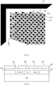
- FIG. 5 a schematic structural diagram of a memory according to an embodiment of the present disclosure is illustrated.
- the memory includes a substrate 100, including an array area 101 and a peripheral area 102 encircling the array area 101. a plurality of discrete active areas 501 arranged in an array are formed in the array area 101.
- the discrete active areas 501 are isolated by shallow trench isolation structures 512, 513, and 511.
- the shallow trench isolation structures 512 and 513 divide the continuous active area into separated discrete active areas 501, and thus the trenches can be formed by carrying out the same etching process once.
- the shallow trench isolation structure 511 isolates different continuous active areas.
- a peripheral shallow trench isolation structure 514 is formed in the peripheral area 102 of the substrate 100, and the peripheral shallow trench isolation structure 514 encircles the array area 101. Between the peripheral shallow trench isolation structure 514 and the array area 101 there is a certain spacing, which serves as an electrical isolation structure between the array area 101 of the substrate and the peripheral area 102.
- a sidewall of the peripheral shallow trench isolation structure 601 (referring to FIG. 6 ) facing toward a side of the array area 101 is a curved surface to reduce the stress effects on the discrete active area 501 at the edge of the array area 101 and to improve the stability.
- the sizes of the shallow trench isolation structures 513 at the ends of a part of outermost discrete active areas 501 are greater than those of shallow trench isolation structures in other positions.
- the discrete active areas 501 are formed by dividing the continuous active areas, and a part of secondary active areas smaller in size than the discrete active areas may be formed at the ends of a part of continuous active areas, which is prone to a problem of collapse.
- the shallow trench isolation structure 513 is formed at the position of the secondary active area to remove the secondary active area. In this way, the problem of collapse of the discrete active area at the edge of the active area array may be improved.
- a shallow trench isolation structure 810 is formed at the end of a peripheral discrete active area formed after other continuous active areas without the secondary active areas are divided, and the size of the shallow trench isolation structure 810 is greater than that of the shallow trench isolation structure 512 in the array area 101.
- the etching load effect caused by different pattern densities can be overcome, the photoetching process window for forming the shallow trench isolation structures 512, 810 and 513 can be increased, and the accuracy of the size of the discrete active area 501 can be improved.
- the sizes of the outermost shallow trench isolation structures 513 and 810 are greater than the size of the shallow trench isolation structure 512 in other positions.
- the smaller-sized secondary active area at the edge of the discrete active area array is removed. Therefore, problems such as collapse due to the smaller-sized secondary active area present at the edge of the discrete active area array may be prevented, and thus the reliability of the memory can be improved.
- a peripheral shallow trench isolation structure for dividing the continuous active area has a larger size, which can avoid the etching load effect in the process of forming a trench by etching. Therefore, the photoetching process window is reduced, and a patterning accuracy in the formation of the shallow trench isolation structure is enhanced, and thus performance of the memory is further improved.
Landscapes
- Engineering & Computer Science (AREA)
- Manufacturing & Machinery (AREA)
- Semiconductor Memories (AREA)
- Element Separation (AREA)
Abstract
Description
- This application claims priority to
Chinese Patent Application No. 201911087070.4, titled "MEMORY AND FORMATION METHOD THEREOF" and filed on November 8, 2019 - The present disclosure relates to the field of memory technologies, and more particularly, to a memory and a formation method thereof.
- A memory includes a plurality of memory cells arranged in an array, and each of the memory cells is formed on an active area (AA). In the process of forming the memory in a prior art, generally it is required to etch a substrate to form the active areas arranged in an array.
- As a memory capacity of the memory increases, a memory density increases, and a line width of the active area gradually shrinks. When a plurality of mask patterns arranged in an array are formed on a surface of the substrate to serve as a mask of the active area, a self-aligned double patterning (SADP) process is required to form an AA mask with a smaller line width pattern to form a strip-shaped AA. Next, a shallow trench isolation (STI) mask is formed on the AA mask to cut off the strip-shaped AA to form the active areas arranged in an array.
- When the SADP process is employed to form the active area of an array area of the memory, a size of the formed active area is very small because the size of the AA mask is small, and thus an edge of an active area array may have problems such as collapse and stress, which may have a negative effect on product yield.
- How to improve the edge problem of the active area array of the memory is a problem to be solved urgently at present.
- A technical problem to be solved by the present disclosure is to provide a memory and a formation method thereof which can improve an edge problem of an active area array of a memory.
- To solve the above problem, the present disclosure provides a formation method of a memory. The method includes: providing a substrate including an array area; forming a first mask layer on a surface of the substrate, wherein a plurality of strip-shaped patterns arranged in parallel are formed in the first mask layer to form, in the array area of the substrate, a plurality of strip-shaped continuous active areas arranged in parallel; forming a second mask layer on the first mask layer, wherein a plurality of first patterns and a plurality of second patterns are formed in the second mask layer, the plurality of first patterns are arranged in an array and are overlapped with the strip-shaped patterns to form division trenches in the substrate to divide the continuous active areas into a plurality of separate discrete active areas arranged in an array, wherein the plurality of second patterns cover ends of a part of the strip-shaped patterns to remove secondary active areas positioned at ends of a part of continuous active areas, wherein the secondary active areas are formed after the continuous active areas are divided by the first patterns and are less than the discrete active areas in length; and performing etching layer by layer into the substrate by using the first mask layer and the second mask layer as masks to transfer the strip-shaped patterns, the first patterns and the second patterns into the substrate to form the plurality of discrete active areas arranged in an array and the division trenches corresponding to the first patterns and the second patterns.
- In some embodiments, the strip-shaped patterns are formed by using an SADP method.
- In some embodiments, the plurality of first patterns include central first patterns and peripheral first patterns, wherein the peripheral first patterns are outermost first pattern, and the central first patterns are positioned at an inner side of the peripheral first pattern. The peripheral first pattern extends outward along a length direction of the strip-shaped pattern, such that a size of the peripheral first pattern is greater than that of the central first pattern.
- In some embodiments, a size of an outermost division trench is greater than sizes of division trenches in other positions.
- In some embodiments, the substrate further includes a peripheral area encircling the array area, and in the second mask layer there is further formed a third pattern positioned on the peripheral area of the substrate and encircling all the strip-shaped patterns. The third pattern is configured for forming, in the peripheral area of the substrate, a peripheral trench encircling the array area.
- In some embodiments, a sidewall of the peripheral trench facing toward a side of the array area is a curved surface.
- In some embodiments, the formation method further includes: filling an insulating material in the division trench and the peripheral trench to form a shallow trench isolation structure.
- The technical solution of the present disclosure also provides a memory, including a substrate, the substrate including an array area. A plurality of discrete active areas arranged in an array are formed in the array area. The discrete active areas are isolated by the shallow trench isolation structure, wherein sizes of at least a part of the outermost shallow trench isolation structures in a length direction of the discrete active area are greater than those of shallow trench isolation structures in other positions in the length direction of the discrete active area.
- In some embodiments, the substrate further includes a peripheral area encircling the array area, a peripheral shallow trench isolation structure is formed in the peripheral area of the substrate, and the peripheral shallow trench isolation structure encircles the array area.
- In some embodiments, the discrete active area is isolated from the peripheral area by the shallow trench isolation structure.
- In some embodiments, a sidewall of the peripheral shallow trench isolation structure facing toward a side of the array area is a curved surface.
- In some embodiments, there is a certain spacing between the peripheral shallow trench isolation structure and the array area.
- In some embodiments, in all the shallow trench isolation structures, the size of the outermost shallow trench isolation structure is greater than those of the shallow trench isolation structures in other positions.
- According to the formation method of a memory provided by the present disclosure, in the process of dividing the continuous active areas, the smaller-sized secondary active area at the edge of the discrete active area array is removed. Therefore, problems such as collapse due to the smaller-sized secondary active area present at the edge of the active area array may be prevented, and thus the reliability of the memory can be improved.
- Further, a peripheral shallow trench isolation structure for dividing the continuous active area has a larger size, which can avoid an etching load effect in the process of forming a trench by etching. Therefore, a photoetching process window is reduced, and a patterning accuracy in the formation of the shallow trench isolation structure is enhanced, and thus performance of the memory is further improved.
-
FIG. 1 to FIG. 8 are schematic structural diagrams showing formation processes of a memory according to some embodiments. - Embodiments of a memory and a formation method thereof provided by the present disclosure are described below in detail with reference to the accompanying drawings.
- With reference to
FIG. 1 , a schematic structural diagram showing formation processes of the memory according to an embodiment of the present disclosure is illustrated. - With reference to
FIG. 1 , asubstrate 100 is provided. Thesubstrate 100 includes anarray area 101 and aperipheral area 102 encircling thearray area 101. - In the
array area 101 there is an active area array for forming a memory, and in theperipheral area 102 there is a peripheral device (such as a logic control circuit) for forming the memory. - With reference to
FIG. 2a andFIG. 2b , afirst mask layer 200 is formed on a surface of thesubstrate 100. A plurality of strip-shaped patterns 201 arranged in parallel are formed in thefirst mask layer 200 and include a strip-shaped pattern 201a and a strip-shaped pattern 201b. The strip-shaped patterns 201 are covered patterns and are configured for forming, in thearray area 101 of thesubstrate 100, a plurality of discrete and strip-shaped continuous active areas arranged in parallel. Between the strip-shaped patterns 201 there is anopening 202, configured for separating the strip-shaped patterns 201.FIG. 2a is a schematic top view, andFIG. 2b is a schematic cross-sectional view along a secant line AA' inFIG. 2a . Before thefirst mask layer 200 is formed, a buffer layer, a hard mask layer or the like may also be formed on the surface of thesubstrate 100 to improve the pattern-transfer accuracy in subsequent etching processes. - The strip-shaped pattern is formed by the SADP method. In one embodiment, with reference to
FIG. 3a to FIG. 3f , schematic structural diagrams showing a method for forming the first mask layer according to an embodiment of the present disclosure are illustrated. - With reference to
FIG. 3a and FIG. 3b , amask pattern 301 is formed on the surface of thesubstrate 100.FIG. 3a is a schematic top view of themask pattern 301, andFIG. 3b is a schematic cross-sectional view along the secant line BB' inFIG. 3a . Themask pattern 301 has strip-shaped patterns arranged in parallel. In this embodiment, themask pattern 301 is arranged obliquely to increase an arrangement density of the discrete active areas formed subsequently. In other embodiments, themask pattern 301 may also be arranged horizontally or vertically. - With reference to
FIG. 3c and FIG. 3d , asidewall 302 is formed on a sidewall of themask pattern 301, and thesidewall 302 encircles the sidewall of themask pattern 301. - With reference to
FIG. 3e , afirst mask material 310 is filled and formed on the surface of thesubstrate 100, and a surface of thefirst mask material 310 is flush with a surface of themask pattern 301. - With reference to
FIG. 3f , thesidewall 302 is removed to form an opening 303 (corresponding to theopening 202 inFIG. 2 ). The mask pattern 301 (corresponding to the strip-shapedpattern 201a inFIG. 2 ) and a mask pattern 311 (corresponding to the strip-shaped pattern 202b inFIG. 2 ) on two sides of the opening are used as strip-shaped patterns to define a width and a length of the continuous active area to be formed in the substrate subsequently. Through the above SADP method, a spacing between adjacent strip-shaped patterns may be reduced, such that a density of the strip-shaped patterns can be increased. - With reference to
FIG. 4a and FIG. 4b , asecond mask layer 400 is formed on thefirst mask layer 200, a plurality offirst patterns 401 and a plurality ofsecond patterns 402 are formed in thesecond mask layer 400. The plurality offirst patterns 401 are arranged in an array and are overlapped with the strip-shapedpatterns substrate 100 so that the continuous active areas are divided into a plurality of discrete active areas arranged in an array. The plurality ofsecond patterns 402 cover ends of a part of the strip-shapedpattern 201a to remove secondary active areas positioned at ends of a part of continuous active areas, wherein the secondary active areas are formed after the continuous active areas are divided by thefirst patterns 401 and are less than the discrete active areas in length. - In
FIG. 4a , only thefirst patterns 401 and thesecond patterns 402 in thesecond mask layer 400 are shown. Thefirst patterns 401 and thesecond patterns 402 are both opening patterns, and the other areas are covered patterns (not shown in the figure).FIG. 4b is a schematic cross-sectional view along a secant line AA' inFIG. 4a . - Before the
second mask layer 400 is formed, it is formed afilling layer 410 that fills up theopening 202 in thefirst mask layer 200 and has a planar surface, and thesecond mask layer 400 is formed on the planar surface of thefilling layer 410. A material of thefilling layer 410 may be an organic anti-reflection layer, silicon oxide or the like. - The
first pattern 401 is an opening pattern, and the strip-shapedpatterns substrate 100 is etched along thefirst pattern 401, a division trench is formed by cutting off the continuous active area correspondingly formed by the strip-shapedpatterns substrate 100. - To increase the memory density, the
first patterns 401 are arranged in staggered rows, such that the discrete active areas formed after division are arranged in staggered rows to increase the number of discrete active areas. This may cause the active areas positioned at ends to be less than the normal discrete active areas in length after a part of continuous active areas are divided, and these active areas with shorter length are referred to as secondary active areas. The secondary active area is unable to form a complete memory cell, and is prone to problems such as collapse. A formation position of the secondary active area generally corresponds to an end of the strip-shapedpattern 201a encircled by theopening 202. - In this embodiment, in the
second mask layer 400 there is further formed asecond pattern 402 which is also an opening pattern. Thesecond pattern 402, covering a position of the end of the strip-shapedpattern 201 corresponding to the secondary active area, is configured for removing the secondary active area, to prevent the problem of collapse of the secondary active area, thereby improving the edge problem of the active area array. - In this embodiment, an end of the strip-shaped
pattern 201b at an outer side of theopening 202 is connected to the first mask layer on the peripheral area of thesubstrate 100. For this reason, an end of the continuous active area correspondingly formed in thesubstrate 100 is connected to the peripheral area of thesubstrate 100, and the problems such as collapse generally do not occur even if the size of the continuous active area is less than that of the discrete active area. Therefore, thesecond pattern 402 generally is formed above the end of the strip-shapedpattern 201 partially encircled by theopening 202. - In other embodiments, in the
second mask layer 400 there is likely formed a pattern cutting off the strip-shapedpattern 201b from the peripheral area, which may cause a consequence that the secondary active area may likely be formed at an end of a formed continuous active area corresponding to the continuousactive area 201b after this continuous active area is divided. Correspondingly, thesecond pattern 402 is also required to be formed on the ends of a part of the strip-shapedpatterns 201b. - In this embodiment, in the
second mask layer 400 there is also formed athird pattern 403 positioned above theperipheral area 102 and encircling all the strip-shapedpatterns third pattern 403 is configured for forming, in theperipheral area 102 of thesubstrate 100, a peripheral trench encircling thearray area 101. Thethird pattern 403 is also an opening pattern. - With reference to
FIG. 5 , it is etched layer by layer into thesubstrate 100 by using thefirst mask layer 200 and thesecond mask layer 400 as masks to transfer the strip-shapedpatterns first pattern 401 and thesecond pattern 402 into thesubstrate 100 to form a plurality of discreteactive areas 501 arranged in an array. Adjacent discrete active areas in the same straight line and adjacent discrete active areas in different straight lines are separated by division trenches. An insulating material is filled in the division trenches to form a shallow trench isolation structure. - The
first pattern 401 corresponds to the shallowtrench isolation structure 512, thesecond pattern 402 corresponds to the shallowtrench isolation structure 513, and theopening 202 corresponds to the shallowtrench isolation structure 511. - Furthermore, in the peripheral area of the
substrate 100 there is also formed a peripheral shallowtrench isolation structure 514 which corresponds to the third pattern 403 (referring toFIG. 4a ). - In another embodiment, a side of the
third pattern 403 facing toward the array area is a curve, such that a sidewall of the formed peripheral shallow trench isolation structure 601 (referring toFIG. 6 ) facing toward the array area is a curved surface. In this way, the total length of the sidewalls can be increased, the stability can be enhanced, the stress generated by the peripheral shallowtrench isolation structure 514 can be further relieved, and the stress effects on the discreteactive area 501 at the edge of the array area can be reduced. - With reference to
FIG. 7 , it is illustrated a schematic diagram after the formation of thesecond mask layer 400 in another embodiment of the present disclosure. - The first patterns in the second mask layer include central
first patterns 401a and peripheralfirst patterns 401b, wherein the peripheralfirst pattern 401b is an outermost first pattern, and the centralfirst pattern 401a is positioned at an inner side of the peripheralfirst pattern 401b. The peripheralfirst pattern 401b extends outward along a length direction of the strip-shapedpatterns first pattern 401b is greater than that of the centralfirst pattern 401a. The peripheral first pattern has a lower pattern density on the outer side, and thus in the etching process, an etching load effect caused by different pattern densities is prone to causing a transfer distortion of the outermost first pattern. Therefore, in this embodiment, by ensuing the size of the peripheralfirst pattern 401b to be greater than that of the centralfirst pattern 401a, the etching load effect can be overcome, a photoetching process window can be increased, and a pattern-transfer accuracy can be improved. - In the embodiment as shown in
FIG. 7 , theperipheral pattern 401a and thesecond pattern 402 correspond to the outermost division trench formed in the array area of the substrate, and the outermost division trench is larger in size than division trenches in other positions. - In other embodiments, in the
second mask layer 400 there also may be not formed thesecond pattern 402, and only the centralfirst pattern 401a and the peripheralfirst pattern 401b are included, to correspondingly form the division trenches for dividing the continuous active areas. - In the foregoing embodiments, the substrate is etched after the formation of a plurality of mask layers having different patterns. In this way, an active area array can be directly formed in the substrate.
- In the embodiments of the present disclosure, there is also provided another method for forming a memory.
- The method for forming a memory includes following steps: providing a substrate, wherein the substrate includes an array area and a peripheral area encircling the array area; forming, in the array area of the substrate, a plurality of discrete and strip-shaped continuous active areas arranged in parallel; forming, in the array area of the substrate, a plurality of division trenches arranged in an array to divide the continuous active areas into a plurality of discrete active areas arranged in an array; and removing secondary active areas positioned at ends of a part of continuous active areas when dividing each of the continuous active areas, wherein the secondary active areas are formed after the continuous active areas are divided and are less than the discrete active areas in length.
- The
first mask layer 200 having the strip-shapedpatterns FIG. 2a may be formed on the surface of the substrate, and then the substrate is etched using thefirst mask layer 200 as a mask to form the strip-shaped continuous active areas in the substrate. - Next, after the
first mask layer 200 is removed, thesecond mask layer 400 having thefirst pattern 401 and thesecond pattern 402 as shown inFIG. 4a and FIG. 4b is formed on the substrate, and then the substrate is etched using thesecond mask layer 400 as a mask. Next, by transferring thefirst pattern 401 and thesecond pattern 402 into the substrate, the continuous active area in the substrate is divided into a plurality of discrete active areas. Because thesecond pattern 402 is formed in thesecond mask layer 400, when each of the continuous active areas is divided, the secondary active areas, which are positioned at the ends of a part of continuous active areas and are less than the discrete active areas in length, are removed. - In other embodiments, after the continuous active area is formed in the substrate, a second mask layer as shown in
FIG. 7 may be further formed on the substrate. The first pattern in the second mask layer includes peripheralfirst patterns 401b and centralfirst patterns 401a. The size of the peripheralfirst pattern 401b is greater than that of the centralfirst pattern 401a, such that the size of the outermost division trench formed in the substrate is greater than that of the division trenches in other positions. - A third pattern may also be formed in the
second mask layer 200. When the division trench is formed, the peripheral area of the substrate is etched to form, in the peripheral area, a peripheral trench encircling the array area. A sidewall of the peripheral trench facing toward a side of the array area may be a curved surface to reduce the stress effects and improve the stability. - Finally, an insulating material is filled in the division trench and the peripheral trench to form a shallow trench isolation structure.
- In the process of forming the memory in this embodiment, the substrate is etched once every time a mask layer is formed, and a discrete active area array is formed by etching the substrate several times.
- An embodiment of the present disclosure also provides a memory formed in the above embodiments.
- With reference to
FIG. 5 , a schematic structural diagram of a memory according to an embodiment of the present disclosure is illustrated. - The memory includes a
substrate 100, including anarray area 101 and aperipheral area 102 encircling thearray area 101. a plurality of discreteactive areas 501 arranged in an array are formed in thearray area 101. The discreteactive areas 501 are isolated by shallowtrench isolation structures trench isolation structures active areas 501, and thus the trenches can be formed by carrying out the same etching process once. The shallowtrench isolation structure 511 isolates different continuous active areas. - A peripheral shallow
trench isolation structure 514 is formed in theperipheral area 102 of thesubstrate 100, and the peripheral shallowtrench isolation structure 514 encircles thearray area 101. Between the peripheral shallowtrench isolation structure 514 and thearray area 101 there is a certain spacing, which serves as an electrical isolation structure between thearray area 101 of the substrate and theperipheral area 102. - In another embodiment, a sidewall of the peripheral shallow trench isolation structure 601 (referring to
FIG. 6 ) facing toward a side of thearray area 101 is a curved surface to reduce the stress effects on the discreteactive area 501 at the edge of thearray area 101 and to improve the stability. - The sizes of the shallow
trench isolation structures 513 at the ends of a part of outermost discreteactive areas 501 are greater than those of shallow trench isolation structures in other positions. The discreteactive areas 501 are formed by dividing the continuous active areas, and a part of secondary active areas smaller in size than the discrete active areas may be formed at the ends of a part of continuous active areas, which is prone to a problem of collapse. The shallowtrench isolation structure 513 is formed at the position of the secondary active area to remove the secondary active area. In this way, the problem of collapse of the discrete active area at the edge of the active area array may be improved. - With reference to
FIG. 8 , in this embodiment, a shallowtrench isolation structure 810 is formed at the end of a peripheral discrete active area formed after other continuous active areas without the secondary active areas are divided, and the size of the shallowtrench isolation structure 810 is greater than that of the shallowtrench isolation structure 512 in thearray area 101. In this way, the etching load effect caused by different pattern densities can be overcome, the photoetching process window for forming the shallowtrench isolation structures active area 501 can be improved. - In
FIG. 8 , the sizes of the outermost shallowtrench isolation structures trench isolation structure 512 in other positions. - In the above memory, the smaller-sized secondary active area at the edge of the discrete active area array is removed. Therefore, problems such as collapse due to the smaller-sized secondary active area present at the edge of the discrete active area array may be prevented, and thus the reliability of the memory can be improved.
- Furthermore, a peripheral shallow trench isolation structure for dividing the continuous active area has a larger size, which can avoid the etching load effect in the process of forming a trench by etching. Therefore, the photoetching process window is reduced, and a patterning accuracy in the formation of the shallow trench isolation structure is enhanced, and thus performance of the memory is further improved.
- What is mentioned above merely refers to some embodiments. It is to be pointed out that to those of ordinary skill in the art, various improvements and embellishments may be made without departing from the principle of the present disclosure, and these improvements and embellishments are also deemed to be within the scope of protection of the present disclosure.
Claims (12)
- A formation method of a memory, comprising:providing a substrate, the substrate comprising an array area;forming a first mask layer on a surface of the substrate, wherein a plurality of strip-shaped patterns arranged in parallel are formed in the first mask layer to form, in the array area of the substrate, a plurality of strip-shaped continuous active areas arranged in parallel;forming a second mask layer on the first mask layer, wherein a plurality of first patterns and a plurality of second patterns are formed in the second mask layer, the plurality of first patterns are arranged in an array and overlapped with the plurality of strip-shaped patterns to form a plurality of division trenches in the substrate to divide the continuous active areas into a plurality of discrete active areas arranged in an array, the plurality of second patterns cover ends of part of the strip-shaped patterns to remove secondary active areas positioned at ends of part of the continuous active areas, wherein the secondary active areas are formed after the continuous active areas are divided by the first patterns and are less than the discrete active areas in length; andperforming etching layer by layer into the substrate by using the first mask layer and the second mask layer as masks to transfer the strip-shaped patterns, the first patterns and the second patterns into the substrate to form a plurality of discrete active areas arranged in an array.
- The formation method according to claim 1, wherein the plurality of strip-shaped patterns are formed by using a self-aligned double patterning (SADP) method.
- The formation method according to claim 1, wherein the plurality of first patterns comprise central first patterns and peripheral first patterns, the peripheral first patterns being outermost first patterns, the central first patterns being positioned at inner sides of the peripheral first patterns, and a peripheral first pattern extending outward along a length direction of a strip-shaped pattern, such that a size of the peripheral first pattern is greater than that of the central first pattern.
- The formation method according to claim 1, wherein a size of an outermost division trench is greater than sizes of the division trenches in other positions.
- The formation method according to claim 4, wherein the substrate further comprises a peripheral area encircling the array area, wherein a third pattern positioned on the peripheral area of the substrate and encircles all the plurality of strip-shaped patterns is formed in the second mask layer, and the third pattern is configured for forming, in the peripheral area of the substrate, a peripheral trench encircling the array area.
- The formation method according to claim 5, wherein a sidewall of the peripheral trench facing toward a side of the array area is a curved surface.
- The formation method according to claim 5, further comprising: filling an insulating material in the division trench and the peripheral trench to form a shallow trench isolation structure.
- A memory, comprising:a substrate, comprising an array area; anda plurality of discrete active areas formed in the array area and arranged in an array;wherein the plurality of discrete active areas are isolated by shallow trench isolation structures, and sizes of at least a part of the outermost shallow trench isolation structures in length direction of the discrete active areas are greater than those of shallow trench isolation structures in other positions in the length direction of the discrete active areas.
- The memory according to claim 8, wherein the substrate further comprises a peripheral area encircling the array area, a peripheral shallow trench isolation structure being formed in the peripheral area, the peripheral shallow trench isolation structure encircling the array area.
- The memory according to claim 9, wherein the discrete active areas are isolated from the peripheral area by the shallow trench isolation structures.
- The memory according to claim 9, wherein a sidewall of the peripheral shallow trench isolation structure facing toward a side of the array area is a curved surface.
- The memory according to claim 9, wherein there is a spacing between the peripheral shallow trench isolation structure and the array area.
Applications Claiming Priority (2)
| Application Number | Priority Date | Filing Date | Title |
|---|---|---|---|
| CN201911087070.4A CN112786443A (en) | 2019-11-08 | 2019-11-08 | Memory and forming method thereof |
| PCT/CN2020/104965 WO2021088431A1 (en) | 2019-11-08 | 2020-07-27 | Memory and forming method therefor |
Publications (2)
| Publication Number | Publication Date |
|---|---|
| EP3933894A1 true EP3933894A1 (en) | 2022-01-05 |
| EP3933894A4 EP3933894A4 (en) | 2022-06-22 |
Family
ID=75748438
Family Applications (1)
| Application Number | Title | Priority Date | Filing Date |
|---|---|---|---|
| EP20885826.6A Pending EP3933894A4 (en) | 2019-11-08 | 2020-07-27 | MEMORY AND ITS FORMATION PROCESS |
Country Status (4)
| Country | Link |
|---|---|
| US (1) | US20210375869A1 (en) |
| EP (1) | EP3933894A4 (en) |
| CN (1) | CN112786443A (en) |
| WO (1) | WO2021088431A1 (en) |
Families Citing this family (3)
| Publication number | Priority date | Publication date | Assignee | Title |
|---|---|---|---|---|
| US12272594B2 (en) * | 2021-05-20 | 2025-04-08 | Fujian Jinhua Integrated Circuit Co., Ltd. | Semiconductor device and method of fabricating the same having a second active region disposed at an outer side of a first active region |
| US12040218B2 (en) * | 2021-07-09 | 2024-07-16 | Winbond Electronics Corp. | Method of forming a semiconductor device |
| CN116206970B (en) * | 2021-11-30 | 2025-07-04 | 长鑫存储技术有限公司 | Semiconductor structure manufacturing method and semiconductor structure |
Family Cites Families (13)
| Publication number | Priority date | Publication date | Assignee | Title |
|---|---|---|---|---|
| US7986042B2 (en) * | 2009-04-14 | 2011-07-26 | Monolithic 3D Inc. | Method for fabrication of a semiconductor device and structure |
| US8637135B2 (en) * | 2009-11-18 | 2014-01-28 | Taiwan Semiconductor Manufacturing Company, Ltd. | Non-uniform semiconductor device active area pattern formation |
| KR101132803B1 (en) * | 2010-12-30 | 2012-04-02 | 주식회사 하이닉스반도체 | Method for fabricating fine pattern |
| KR102046504B1 (en) * | 2013-01-17 | 2019-11-19 | 삼성전자주식회사 | Step shape pad structure and wiring structure in vertical type semiconductor device |
| US20140264726A1 (en) * | 2013-03-13 | 2014-09-18 | Macronix International Co., Ltd. | Structure and method for protected periphery semiconductor device |
| KR102280471B1 (en) * | 2015-07-20 | 2021-07-22 | 삼성전자주식회사 | Method of forming active patterns, active pattern array, and method of manufacturing semiconductor device |
| US10056395B2 (en) * | 2016-03-29 | 2018-08-21 | Macronix International Co., Ltd. | Method of improving localized wafer shape changes |
| CN107818980B (en) * | 2016-09-12 | 2019-07-05 | 联华电子股份有限公司 | Active area structure and forming method thereof |
| US20190139766A1 (en) * | 2017-11-09 | 2019-05-09 | Nanya Technology Corporation | Semiconductor structure and method for preparing the same |
| CN207503954U (en) * | 2017-12-01 | 2018-06-15 | 睿力集成电路有限公司 | Fleet plough groove isolation structure array, semiconductor device structure |
| US10192837B1 (en) * | 2017-12-20 | 2019-01-29 | Nxp B.V. | Multi-via redistribution layer for integrated circuits having solder balls |
| CN208819860U (en) * | 2018-09-12 | 2019-05-03 | 长鑫存储技术有限公司 | Fleet plough groove isolation structure and semiconductor devices |
| CN210607187U (en) * | 2019-11-08 | 2020-05-22 | 长鑫存储技术有限公司 | memory |
-
2019
- 2019-11-08 CN CN201911087070.4A patent/CN112786443A/en active Pending
-
2020
- 2020-07-27 EP EP20885826.6A patent/EP3933894A4/en active Pending
- 2020-07-27 WO PCT/CN2020/104965 patent/WO2021088431A1/en not_active Ceased
-
2021
- 2021-08-13 US US17/401,328 patent/US20210375869A1/en not_active Abandoned
Also Published As
| Publication number | Publication date |
|---|---|
| CN112786443A (en) | 2021-05-11 |
| US20210375869A1 (en) | 2021-12-02 |
| WO2021088431A1 (en) | 2021-05-14 |
| EP3933894A4 (en) | 2022-06-22 |
Similar Documents
| Publication | Publication Date | Title |
|---|---|---|
| US11894420B2 (en) | Memory and formation method thereof | |
| US20210375869A1 (en) | Memory and formation method thereof | |
| US9704816B1 (en) | Active region structure and forming method thereof | |
| US9147612B2 (en) | Method for forming a semiconductor structure | |
| CN110676259B (en) | Three-dimensional storage structure and manufacturing method thereof | |
| US11972953B2 (en) | Semiconductor structure and manufacturing method thereof | |
| KR101094486B1 (en) | Pattern formation method of semiconductor device | |
| CN210607188U (en) | Memory device | |
| KR102637621B1 (en) | Method for manufacturing semiconductor device | |
| CN111863826B (en) | Manufacturing method of graphical mask and manufacturing method of three-dimensional NAND memory | |
| CN111430361A (en) | A kind of manufacturing method of 3D NAND memory device | |
| CN210607187U (en) | memory | |
| US6953973B2 (en) | Self-aligned trench isolation method and semiconductor device fabricated using the same | |
| CN113471194B (en) | semiconductor storage device | |
| KR100819559B1 (en) | Semiconductor integrated circuit devices and their formation methods having a gate pattern located between electrical nodes and adapted to physically space the nodes on a semiconductor substrate | |
| CN112992915B (en) | Three-dimensional memory and manufacturing method thereof | |
| KR101917392B1 (en) | Semiconductor device and method of manufacturing the same | |
| US20230232620A1 (en) | Memory device and manufacturing method thereof | |
| CN209880617U (en) | Electronic element structure | |
| CN215342596U (en) | Semiconductor memory device with a plurality of memory cells | |
| US9368365B1 (en) | Method for forming a semiconductor structure | |
| KR20120038070A (en) | Semiconductor device and method for fabricating the same | |
| CN115701214B (en) | Method for manufacturing bit line structure and method for manufacturing data storage array | |
| KR20120034935A (en) | Semiconductor device manufacturing method | |
| CN114944401A (en) | Three-dimensional memory, manufacturing method thereof and storage system |
Legal Events
| Date | Code | Title | Description |
|---|---|---|---|
| STAA | Information on the status of an ep patent application or granted ep patent |
Free format text: STATUS: THE INTERNATIONAL PUBLICATION HAS BEEN MADE |
|
| PUAI | Public reference made under article 153(3) epc to a published international application that has entered the european phase |
Free format text: ORIGINAL CODE: 0009012 |
|
| STAA | Information on the status of an ep patent application or granted ep patent |
Free format text: STATUS: REQUEST FOR EXAMINATION WAS MADE |
|
| 17P | Request for examination filed |
Effective date: 20210930 |
|
| AK | Designated contracting states |
Kind code of ref document: A1 Designated state(s): AL AT BE BG CH CY CZ DE DK EE ES FI FR GB GR HR HU IE IS IT LI LT LU LV MC MK MT NL NO PL PT RO RS SE SI SK SM TR |
|
| A4 | Supplementary search report drawn up and despatched |
Effective date: 20220523 |
|
| RIC1 | Information provided on ipc code assigned before grant |
Ipc: H01L 27/108 20060101ALI20220517BHEP Ipc: H01L 21/762 20060101ALI20220517BHEP Ipc: H01L 21/308 20060101AFI20220517BHEP |
|
| DAV | Request for validation of the european patent (deleted) | ||
| DAX | Request for extension of the european patent (deleted) |