EP3933889A1 - Buried gate preparation method and semiconductor device preparation method - Google Patents
Buried gate preparation method and semiconductor device preparation method Download PDFInfo
- Publication number
- EP3933889A1 EP3933889A1 EP21773282.5A EP21773282A EP3933889A1 EP 3933889 A1 EP3933889 A1 EP 3933889A1 EP 21773282 A EP21773282 A EP 21773282A EP 3933889 A1 EP3933889 A1 EP 3933889A1
- Authority
- EP
- European Patent Office
- Prior art keywords
- trench
- layer
- manufacturing
- conductive layer
- gate
- Prior art date
- Legal status (The legal status is an assumption and is not a legal conclusion. Google has not performed a legal analysis and makes no representation as to the accuracy of the status listed.)
- Granted
Links
Images





Classifications
-
- H—ELECTRICITY
- H10—SEMICONDUCTOR DEVICES; ELECTRIC SOLID-STATE DEVICES NOT OTHERWISE PROVIDED FOR
- H10D—INORGANIC ELECTRIC SEMICONDUCTOR DEVICES
- H10D64/00—Electrodes of devices having potential barriers
- H10D64/20—Electrodes characterised by their shapes, relative sizes or dispositions
- H10D64/27—Electrodes not carrying the current to be rectified, amplified, oscillated or switched, e.g. gates
- H10D64/311—Gate electrodes for field-effect devices
- H10D64/411—Gate electrodes for field-effect devices for FETs
- H10D64/511—Gate electrodes for field-effect devices for FETs for IGFETs
- H10D64/512—Disposition of the gate electrodes, e.g. buried gates
- H10D64/513—Disposition of the gate electrodes, e.g. buried gates within recesses in the substrate, e.g. trench gates, groove gates or buried gates
-
- H—ELECTRICITY
- H10—SEMICONDUCTOR DEVICES; ELECTRIC SOLID-STATE DEVICES NOT OTHERWISE PROVIDED FOR
- H10B—ELECTRONIC MEMORY DEVICES
- H10B12/00—Dynamic random access memory [DRAM] devices
- H10B12/01—Manufacture or treatment
- H10B12/02—Manufacture or treatment for one transistor one-capacitor [1T-1C] memory cells
- H10B12/05—Making the transistor
- H10B12/053—Making the transistor the transistor being at least partially in a trench in the substrate
-
- H—ELECTRICITY
- H10—SEMICONDUCTOR DEVICES; ELECTRIC SOLID-STATE DEVICES NOT OTHERWISE PROVIDED FOR
- H10B—ELECTRONIC MEMORY DEVICES
- H10B12/00—Dynamic random access memory [DRAM] devices
- H10B12/30—DRAM devices comprising one-transistor - one-capacitor [1T-1C] memory cells
- H10B12/34—DRAM devices comprising one-transistor - one-capacitor [1T-1C] memory cells the transistor being at least partially in a trench in the substrate
-
- H—ELECTRICITY
- H10—SEMICONDUCTOR DEVICES; ELECTRIC SOLID-STATE DEVICES NOT OTHERWISE PROVIDED FOR
- H10B—ELECTRONIC MEMORY DEVICES
- H10B12/00—Dynamic random access memory [DRAM] devices
- H10B12/30—DRAM devices comprising one-transistor - one-capacitor [1T-1C] memory cells
- H10B12/48—Data lines or contacts therefor
- H10B12/488—Word lines
-
- H—ELECTRICITY
- H10—SEMICONDUCTOR DEVICES; ELECTRIC SOLID-STATE DEVICES NOT OTHERWISE PROVIDED FOR
- H10D—INORGANIC ELECTRIC SEMICONDUCTOR DEVICES
- H10D30/00—Field-effect transistors [FET]
- H10D30/01—Manufacture or treatment
- H10D30/021—Manufacture or treatment of FETs having insulated gates [IGFET]
-
- H—ELECTRICITY
- H10—SEMICONDUCTOR DEVICES; ELECTRIC SOLID-STATE DEVICES NOT OTHERWISE PROVIDED FOR
- H10D—INORGANIC ELECTRIC SEMICONDUCTOR DEVICES
- H10D64/00—Electrodes of devices having potential barriers
- H10D64/01—Manufacture or treatment
- H10D64/025—Manufacture or treatment forming recessed gates, e.g. by using local oxidation
- H10D64/027—Manufacture or treatment forming recessed gates, e.g. by using local oxidation by etching at gate locations
-
- H—ELECTRICITY
- H10—SEMICONDUCTOR DEVICES; ELECTRIC SOLID-STATE DEVICES NOT OTHERWISE PROVIDED FOR
- H10D—INORGANIC ELECTRIC SEMICONDUCTOR DEVICES
- H10D64/00—Electrodes of devices having potential barriers
- H10D64/20—Electrodes characterised by their shapes, relative sizes or dispositions
- H10D64/27—Electrodes not carrying the current to be rectified, amplified, oscillated or switched, e.g. gates
- H10D64/311—Gate electrodes for field-effect devices
- H10D64/411—Gate electrodes for field-effect devices for FETs
- H10D64/511—Gate electrodes for field-effect devices for FETs for IGFETs
- H10D64/512—Disposition of the gate electrodes, e.g. buried gates
-
- H—ELECTRICITY
- H10—SEMICONDUCTOR DEVICES; ELECTRIC SOLID-STATE DEVICES NOT OTHERWISE PROVIDED FOR
- H10P—GENERIC PROCESSES OR APPARATUS FOR THE MANUFACTURE OR TREATMENT OF DEVICES COVERED BY CLASS H10
- H10P14/00—Formation of materials, e.g. in the shape of layers or pillars
- H10P14/20—Formation of materials, e.g. in the shape of layers or pillars of semiconductor materials
-
- H—ELECTRICITY
- H10—SEMICONDUCTOR DEVICES; ELECTRIC SOLID-STATE DEVICES NOT OTHERWISE PROVIDED FOR
- H10W—GENERIC PACKAGES, INTERCONNECTIONS, CONNECTORS OR OTHER CONSTRUCTIONAL DETAILS OF DEVICES COVERED BY CLASS H10
- H10W10/00—Isolation regions in semiconductor bodies between components of integrated devices
- H10W10/01—Manufacture or treatment
- H10W10/011—Manufacture or treatment of isolation regions comprising dielectric materials
- H10W10/014—Manufacture or treatment of isolation regions comprising dielectric materials using trench refilling with dielectric materials, e.g. shallow trench isolations
-
- H—ELECTRICITY
- H10—SEMICONDUCTOR DEVICES; ELECTRIC SOLID-STATE DEVICES NOT OTHERWISE PROVIDED FOR
- H10W—GENERIC PACKAGES, INTERCONNECTIONS, CONNECTORS OR OTHER CONSTRUCTIONAL DETAILS OF DEVICES COVERED BY CLASS H10
- H10W10/00—Isolation regions in semiconductor bodies between components of integrated devices
- H10W10/10—Isolation regions comprising dielectric materials
- H10W10/17—Isolation regions comprising dielectric materials formed using trench refilling with dielectric materials, e.g. shallow trench isolations
-
- H—ELECTRICITY
- H10—SEMICONDUCTOR DEVICES; ELECTRIC SOLID-STATE DEVICES NOT OTHERWISE PROVIDED FOR
- H10D—INORGANIC ELECTRIC SEMICONDUCTOR DEVICES
- H10D64/00—Electrodes of devices having potential barriers
- H10D64/01—Manufacture or treatment
-
- H—ELECTRICITY
- H10—SEMICONDUCTOR DEVICES; ELECTRIC SOLID-STATE DEVICES NOT OTHERWISE PROVIDED FOR
- H10P—GENERIC PROCESSES OR APPARATUS FOR THE MANUFACTURE OR TREATMENT OF DEVICES COVERED BY CLASS H10
- H10P14/00—Formation of materials, e.g. in the shape of layers or pillars
- H10P14/20—Formation of materials, e.g. in the shape of layers or pillars of semiconductor materials
- H10P14/24—Formation of materials, e.g. in the shape of layers or pillars of semiconductor materials using chemical vapour deposition [CVD]
-
- H—ELECTRICITY
- H10—SEMICONDUCTOR DEVICES; ELECTRIC SOLID-STATE DEVICES NOT OTHERWISE PROVIDED FOR
- H10P—GENERIC PROCESSES OR APPARATUS FOR THE MANUFACTURE OR TREATMENT OF DEVICES COVERED BY CLASS H10
- H10P14/00—Formation of materials, e.g. in the shape of layers or pillars
- H10P14/20—Formation of materials, e.g. in the shape of layers or pillars of semiconductor materials
- H10P14/34—Deposited materials, e.g. layers
- H10P14/3402—Deposited materials, e.g. layers characterised by the chemical composition
- H10P14/3404—Deposited materials, e.g. layers characterised by the chemical composition being Group IVA materials
- H10P14/3411—Silicon, silicon germanium or germanium
Definitions
- the disclosure relates to a method for manufacturing a buried gate and a method for manufacturing a semiconductor device.
- a trench is provided on an active area of a substrate.
- a gate structure is filled in a bottom of the trench, and a trench sidewall above the gate structure is exposed.
- An epitaxial layer is grown on the exposed trench sidewall with an epitaxial growth process, which dose not close the trench.
- the dielectric layer 121 may be formed by using a deposition process.
- the dielectric layer 121 shape-retaining covers the exposed surface.
- the socalled “shape-retaining coverage” refers to that the thickness of the dielectric layer 121 is uniform and consistent.
- the dielectric layer 121 is respectively formed on the inner wall of the trench, on the substrate 100 out of the trench and on the isolation structure 110.
- the deposition process may specifically use chemical vapor deposition (CVD) or atomic layer deposition (ALD).
- the CVD may use plasma enhancing CVD (PECVD), and may also use other appropriate deposition process.
- the formed dielectric layer 121 may be an oxide, and may also be a nitride.
- the trench sidewall when only the protective layer 130 is formed on the trench sidewall, by just removing the protective layer 130 on the sidewall the trench sidewall can be exposed.
- the other structure on the sidewall when other structure is clamped between the trench sidewall and the protective layer, after the protective layer 130 is removed, the other structure on the sidewall is exposed, and the exposed other structure needs to be further etched till the trench sidewall themselves are exposed.
- the formed dielectric layer 121 that covers the inner wall of the trench and the upper surface of the substrate 100 out of the trench, is not removed before Step S222, then in Step S222, the dielectric layer 121 on the trench sidewall is exposed after the protective layer 130 on the trench sidewall is removed. T this time, the dielectric layer 121 is further etched till the trench sidewall is exposed.
- in-situ cleaning is performed on the exposed surface of the trench sidewall of the substrate 100, to remove impurities on the surface of the substrate 100.
- SiCoNi in-situ precleaning may be performed, and other dry cleaning or separated wet etching may also be used.
- Step S330 the temperature is lowered to 715°C to 725°C and a pressure is lowered to 9 torr to 11 torr, and then epitaxial growth reaction gases are charged for a preset period for the epitaxial growth. Specifically, the temperature in the furnace chamber is lowered to 715°C to 725°C and the pressure is lowered to 9 torr to 11 torr, and then the epitaxial growth reaction gases are charged.
- the reaction gases may be a combination of SiH 4 , HCl and hydrogen, a combination of SiCl 4 and hydrogen or a combination of SiHCl 3 and hydrogen.
- the residual reaction gases and reaction product gases need to be pumped out continuously.
Landscapes
- Engineering & Computer Science (AREA)
- Manufacturing & Machinery (AREA)
- Insulated Gate Type Field-Effect Transistor (AREA)
- Electrodes Of Semiconductors (AREA)
Abstract
Description
- The present application claims priority to
Chinese Patent Application No. 202010365052.4, filed on April 30, 2020 - The disclosure relates to a method for manufacturing a buried gate and a method for manufacturing a semiconductor device.
- During manufacture of transistors, the level of integration for chips is improved by forming buried gates. The buried gate is formed by providing a trench in a substrate and filling a gate structure in the trench.
- With further improvements of requirements on the level of integration, a width of a trench in which the gate structure is filled is increasingly narrower.
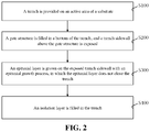
- According to various examples, an aspect of the disclosure provides a method for manufacturing a buried gate, which includes the following operations.
- A trench is provided on an active area of a substrate.
- A gate structure is filled in a bottom of the trench, and a trench sidewall above the gate structure is exposed.
- An epitaxial layer is grown on the exposed trench sidewalls with an epitaxial growth process, which does not close the trench.
- An isolation layer is filled in the trench.
- Another aspect of the disclosure provides a method for manufacturing a semiconductor device, which includes the following operations.
- A gate structure is manufactured on a substrate with the above method for manufacturing the buried gate.
- An active area on each of two sides of the gate structure is doped to form a source/drain region.
- Details of one or more examples of the present application are proposed in the following accompanying drawings and descriptions. Other features and advantages of the disclosure will be apparent in the descriptions, accompanying drawings and claims.
- To illustrate the technical solutions in the examples of the disclosure more clearly, the accompanying drawings for describing the examples are introduced briefly in the following. Apparently, the accompanying drawings in the following description are only about some examples of the disclosure, and those of ordinary skill in the art can derive other drawings from these accompanying drawings without creative efforts.
-
FIG. 1 illustrates a structural schematic diagram after a buried gate is manufactured in a substrate according to the conventional technique. -
FIG. 2 illustrates a flowchart of steps of a method for manufacturing a buried gate according to an example. -
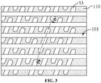
FIG. 3 illustrates a top view of a trench penetrating through an active area according to an example. -
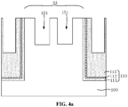
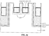
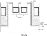
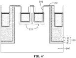
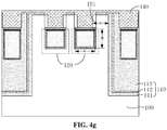
FIG. 4a to FIG. 4g illustrate a structural schematic diagram corresponding to the related steps of a method for manufacturing a buried gate according to an example. -
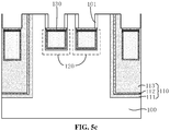
FIG. 5a to FIG. 5c illustrate a structural schematic diagram corresponding to the related steps for growing an epitaxial layer on trench sidewalls according to another example. - Substrate: 100; active area: AA; trench: 101; isolation structure: 110; first isolation layer: 111; second isolation layer: 112; third isolation layer: 113; protective layer: 130; isolation layer: 140; gate structure: 120; dielectric layer: 121; metal nitride layer: 122; first conductive layer: 123; polysilicon layer: 124; epitaxial layer: 101; height of the gate conductive layer: HI; width of the gate conductive layer: W1; and width of the active area on a side of the trench: W2.
- When the width of the trench is reduced to a certain extent, it is hard to fill the gate structure in the trench. Meanwhile, while the width of the trench is reduced, the width of the gate structure is reduced, which results in that the resistance of the gate conductive layer is increased and the electrical performance of the transistor is decreased.
- For the ease of understanding the disclosure, the disclosure is described more completely with reference to related accompanying drawings. Preferred examples of the disclosure are given in the accompanying drawings. However, the disclosure may be implemented in many different forms and is not limited to the examples described herein. Conversely, these examples are provided to make the disclosures of the disclosure more thoroughly and completely.
- Unless otherwise defined, all technical and scientific terms used in the specification have a same meaning generally understood by a person skilled in the art to which the disclosure belongs. The terms used in the specification of the disclosure are merely to describe the specific examples, rather than to limit the disclosure. The term "and/or" used herein includes one or any or all possible combinations of multiple associated items that are listed.
- In the conventional art, as shown in
FIG. 1 , the process for forming the buried gate on the substrate 100' includes that: a trench is provided on the substrate 100', a gate structure 110' is filled in a bottom of the trench, and then an isolation layer 140' is directly deposited to fully fill the trench above the gate structure 110'. For the buried gate formed in the conventional art, the gate conductive layer has a width of W1', and a height of HI'. According to the resistance formula R=ρ*L/(W*H), the resistance of the gate conductive layer is inversely proportional to the width of the gate conductive layer. Therefore, the narrower the opening of the trench, and the narrower the gate conductive layer, thereby the larger the resistance. - In view of this, the disclosure relates to a method for manufacturing a buried gate. The method for manufacturing the buried gate may at least include the following several steps.
- A trench is provided on an active area of a substrate.
- A gate structure is filled in a bottom of the trench, and a trench sidewall above the gate structure is exposed.
- An epitaxial layer is grown on the exposed trench sidewall with an epitaxial growth process, which dose not close the trench.
- An isolation layer is filled in the trench.
- According to the method for manufacturing the buried gate, the trench is provided on the substrate, the trench may be divided into a bottom trench and a top trench that are communicated to each other, and the gate structure is filled in the bottom groove but not in the top groove, such that the top trench sidewall is exposed, and the epitaxial layer is grown on the top trench sidewall with an epitaxial growth technique. In the disclosure, the trench having an opening with a large width may be first provided on the substrate, in which the gate structure is filled; and after the gate structure is filled, the epitaxial layer is grown on the top trench sidewall with the epitaxial growth technique. The width of the active area at each of two sides of the gate structure is increased by the epitaxial layer. In the disclosure, the trench having the large opening is first provided in which the gate structure is filled, and then the width of the opening of the trench above the gate structure is reduced by the epitaxial growth technique. Compared with the conventional art in which the trench having a small opening is directly provided, when area of the active area on each of the two sides of the trench are unchanged, and the depth of the trench and the length of the trench are unchanged, the width of the buried gate formed in the disclosure is increased, i.e., the width of the gate conductive layer is increased, and the resistance of the gate conductive layer is reduced, such that the manufactured buried gate has good electrical performance.
- The method for manufacturing the buried gate in the disclosure will be described below in detail with specific examples.
- As shown in
Fig. 2 , the method for manufacturing the buried gate in the disclosure may include the following steps. - In Step S100: a trench is provided on an active area of a substrate.
- As shown in
FIG. 3 andFIG. 4a, FIG. 4a is a side sectional view along a BB' section line inFIG. 3 . The active area AA is defined on thesubstrate 100, and thetrench 101 is provided on the active area AA. Specifically, there may be onetrench 101, and may also be multipleparallel trenches 101, which may have the same size or different sizes. Thetrench 101 in the active area AA may extend along a direction parallel to a surface of the substrate 100 (a length direction of the trench) to two sides to penetrate through the active area AA. - The
substrate 100 may be one of a silicon wafer, a germanium wafer, a silicon-on-insulator (SOI) wafer, a germanium-on-insulator (GOI) wafer, a silicon-germanium wafer and a substrate formed with anepitaxial layer 101. In this example, thesubstrate 100 uses the silicon wafer. - Specifically, the trench is provided on the
substrate 100, which may be implemented by first forming a mask layer on thesubstrate 100, defining an etching pattern with the mask layer, and then etching thesubstrate 100 by an etching process to provide the trench. The mask layer may be a hard mask, and may specifically use silicon nitride or silicon oxide. Specifically, the trench may be formed with a self-aligned quadruple patterning (SAQP) process. With the technique of SAQP, the small-sized structure may be obtained. - In an example, an
isolation structure 110 is further formed on thesubstrate 100. Theisolation structure 110 is formed by filling a dielectric layer in an isolation trench. Adjacent active areas AA are electrically isolated by theisolation structure 110. Specifically, before Step S100, theisolation structure 110 may be formed on thesubstrate 100 and the active area AA may be defined by theisolation structure 110. Theisolation structure 110 may be the silicon nitride or the silicon oxide, and may also be a composite structure of the silicon nitride and the silicon oxide. In the example, theisolation structure 110 includes afirst isolation layer 111 formed on an inner wall of the isolation trench, asecond isolation layer 112 covering thefirst isolation layer 111 and athird isolation layer 113 covering thesecond isolation layer 112 and fully filling the isolation trench. Thefirst isolation layer 111 and thethird isolation layer 113 may be silicon oxide, thesecond isolation layer 112 may be silicon nitride, and thus theisolation structure 110 is of a silicon oxide-silicon nitride-silicon oxide composite isolation structure. In an example, while the trench is provided on the active area AA, a trench is also correspondingly provided on theisolation structure 110, and while the trench on the active area AA is filled with the following steps, the trench on theisolation structure 110 is also filled with the same steps. - In Step S200: a gate structure is filled in a bottom of the trench, and a trench sidewall above the gate structure is exposed.
- The gate structure is filled in the bottom of the trench with a preset thickness. The gate structure does not fully fill the trench. The trench portion filled with the gate structure is defined as the bottom trench, and the trench portion above the bottom trench is defined as the top trench. By this time, the gate structure is only filled in the bottom trench but does not filled in the top trench, thereby forming the buried gate. After the gate structure is formed, there is a need to expose the trench sidewalls above the gate structure outside.
- In an example, the gate structure is filled in the bottom of the trench, which may include the following steps.
- In Step S211: a dielectric layer is formed on an inner wall of the trench.
- As shown in
FIG. 4b , thedielectric layer 121 is formed on the inner wall of the trench, with which the gate dielectric layer is formed. - In an example, the
dielectric layer 121 may be formed by using a deposition process. Thedielectric layer 121 shape-retaining covers the exposed surface. The socalled "shape-retaining coverage" refers to that the thickness of thedielectric layer 121 is uniform and consistent. As shown inFIG. 4b , thedielectric layer 121 is respectively formed on the inner wall of the trench, on thesubstrate 100 out of the trench and on theisolation structure 110. The deposition process may specifically use chemical vapor deposition (CVD) or atomic layer deposition (ALD). The CVD may use plasma enhancing CVD (PECVD), and may also use other appropriate deposition process. Specifically, the formeddielectric layer 121 may be an oxide, and may also be a nitride. - In another example, the
dielectric layer 121 may also be formed by using a thermal oxidation process. With the thermal oxidation process, an oxide layer may be formed on the surface of the exposedsubstrate 100 and on the inner wall of the trench. Therefore, the oxide layer formed on the inner wall of the trench and on the surface of thesubstrate 100 out of the trench may serve as thedielectric layer 121. - In an example, as shown in
FIG. 4b , after thedielectric layer 121 is formed on the inner wall of the trench, and before Step S220, the method further includes that: ametal nitride layer 122 is formed on thedielectric layer 121. Specifically, themetal nitride layer 122 includes titanium nitride. - In Step S212: a first conductive layer is filled in the trench, and the first conductive layer is back-etched to a preset depth.
- Further referring to
FIG. 4b , the firstconductive layer 123 is filled in the trench. Specifically, the firstconductive layer 123 may be deposited with a deposition process. The deposition process may also be the above described any deposition process. The firstconductive layer 123 deposited herein is relatively thick, thus it overflows from the trench for a certain height after fully filling the trench. Further, the step that the firstconductive layer 123 is back-etched includes that: first, the firstconductive layer 123 is ground with a grinding process to remove the firstconductive layer 123 out of the trench, and then the firstconductive layer 123 in the trench is etched to a preset depth with a dry etching process. Thus, thegate structure 120 includes the firstconductive layer 123 and thedielectric layer 121 clamped between the firstconductive layer 123 and the inner wall of the trench, in which the firstconductive layer 123 serves as the gate conductive layer, and the portion of thedielectric layer 121 clamped between the firstconductive layer 123 and the inner wall of the trench is the gate dielectric layer. - In an example, the first
conductive layer 123 uses a metal having good conductivity. For example, tungsten, molybdenum, cobalt, ruthenium, copper, silver, aluminum, tungsten-copper alloy, graphene and the like may be used as low-resistivity materials. The firstconductive layer 123 may use a material selected from the above materials but is not limited thereto. It may also use other appropriate conductive material. - In an example, when the
metal nitride layer 122 is further formed on thedielectric layer 121, after the firstconductive layer 123 is filled, both the firstconductive layer 123 and themetal nitride layer 122 are back-etched to a preset depth. Specifically, the firstconductive layer 123 and themetal nitride layer 122 may be back-etched to the preset depth at the same time, such that upper surface of the firstconductive layer 123 and themetal nitride layer 122 are flush. - In an example, after the first
conductive layer 123 is back-etched, thedielectric layer 121 may also be further back-etched to the preset depth, to remove thedielectric layer 121 other than that in thegate structure 120. In another example, after the firstconductive layer 123 is back-etched, thedielectric layer 121 is not back-etched, but retained on the trench sidewall above thegate structure 120 and on the surface of thesubstrate 100 out of the trench. - In an example, when the first
conductive layer 123 is metal, after the firstconductive layer 123 is back-etched to the preset depth, the method may further include that: apolysilicon layer 124 covering the firstconductive layer 123 is formed in the trench, which does not fully fill the trench. At this time, thegate structure 120 includes thepolysilicon layer 124, the firstconductive layer 123, themetal nitride layer 122 and thedielectric layer 121 clamped between themetal nitride layer 122 and the inner wall of the trench. During the specific process, the relativelythick polysilicon layer 124 may be deposited in the trench with the deposition process, and then thepolysilicon layer 124 is back-etched to a target thickness. At this time, as shown inFIG. 4c , thepolysilicon layer 124 covers the firstconductive layer 123 and does not fully fill the trench. In this example, by forming thepolysilicon layer 124 on the firstconductive layer 123, thepolysilicon layer 124 has a small work function, thus may reduce the gate-induced leakage. In other examples, materials such as Al, Ta, Nb and Zr may also be used to replace thepolysilicon layer 124. - In an example, after the
gate structure 120 is filled in the bottom of the trench, the method may further include the following step. - In Step S220: a protective layer covering the upper surface of the gate structure and exposing the trench sidewall above the gate structure is formed.
- In an example, Step S220 may be divided into the following sub-steps.
- In Step S221: a protective layer covering the trench sidewall, an upper surface of the gate structure and an upper surface of the substrate out of the trench is formed.
- As shown in
FIG. 4d , theprotective layer 130 with an uniform thickness is deposited on the structural surfaces in the trench and out of the trench with a deposition process. At this time, theprotective layer 130 shape-retaining covers the trench sidewall, the upper surface of thegate structure 120 and the upper surface of thesubstrate 100 out of the trench. Specifically, the deposition process is the ALD process. - In Step S222: with an etching process, the protective layer on the trench sidewall is removed and the protective layer covering the upper surface of the gate structure is retained.
- In an example, the etching process is lateral etching. As shown in
FIG. 4e , after theprotective layer 130 is deposited, theprotective layer 130 is laterally etched to remove theprotective layer 130 on the trench sidewall, meanwhile retain theprotective layers 130 on the upper surface of thegate structure 120 and on the upper surface of thesubstrate 100 out of the trench, such that only the substrate on the trench sidewall is exposed, therefore, in the subsequent epitaxial growth process, the epitaxial layer is only formed on the trench sidewalls. In other examples, as shown inFIG. 5a , the protective layer on the trench sidewall and on the upper surface of the substrate out of the trench may be removed together, while only theprotective layer 130 on the upper surface of thegate structure 120 is retained, such that the trench sidewall and the substrate out of the trench are exposed at the same time, therefore, in the subsequent epitaxial growth process, the epitaxial layer is formed on the trench sidewall and the substrate out of the trench at the same time; and after the epitaxial growth, the excessive epitaxial layer out of the trench may be removed with the grinding process. - The lateral etching may be wet etching which as a relatively larger etching rate to the sidewall. For example, after the
substrate 100 is placed into an etchant, an external electric field is applied to a space where the etchant is present. Depending on the applied external electric field, corrosive negative ions and/or positive ions in the etchant are driven to a direction to be etched. In the example, the direction to be etched is a horizontal direction (lateral) toward the trench sidewall. By controlling the direction of the wet etching, the etching selectivity of the wet etching is improved. Theprotective layer 130 on the trench sidewall is etched, whereas the degree of etching on theprotective layers 130 covering the upper surface of thegate structure 120 and the upper surface of thesubstrate 100 is relatively low, such that after theprotective layer 130 on the trench sidewall is etched completely and the trench sidewall are exposed, the upper surface of thegate structure 120 and the upper surface of thesubstrate 100 are still covered by the protective layers 130. Specifically, theprotective layer 130 may be silicon nitride or silicon oxide, and may also be other appropriate dielectric material. - In an example, when only the
protective layer 130 is formed on the trench sidewall, by just removing theprotective layer 130 on the sidewall the trench sidewall can be exposed. In another example, when other structure is clamped between the trench sidewall and the protective layer, after theprotective layer 130 is removed, the other structure on the sidewall is exposed, and the exposed other structure needs to be further etched till the trench sidewall themselves are exposed. For example, when thegate structure 120 is manufactured, the formeddielectric layer 121, that covers the inner wall of the trench and the upper surface of thesubstrate 100 out of the trench, is not removed before Step S222, then in Step S222, thedielectric layer 121 on the trench sidewall is exposed after theprotective layer 130 on the trench sidewall is removed. T this time, thedielectric layer 121 is further etched till the trench sidewall is exposed. - In the above example, after a protective layer is formed, the protective layer on the sidewall is removed and the
protective layer 130 covering thegate structure 120 is retained to expose the trench sidewall above thegate structure 120. In another example, theprotective layer 130 may be only deposited in a target region by a patterning deposition technique. For example, theprotective layer 130 is only deposited on thegate structure 120 and on the structural surface out of the trench but not deposited on the trench sidewall above thegate structure 120, such that the trench sidewall above thegate structure 120 retains being exposed. In still another example, the protective layer may also be fully filled in the trench above thegate structure 120, then the protective layer is back-etched to reduce its height, and a part of protective layer on the top of the trench is removed. As shown inFIG. 5a , only a part of the protective layer is retained to cover the gate structure. - In Step S300: an epitaxial layer is grown on the exposed trench sidewall with an epitaxial growth process, which does not close the trench.
- As shown in
FIG. 4f , theepitaxial layer 101 is grown on the exposed trench sidewall with the epitaxial growth process, and theepitaxial layer 101 does not close the trench, i.e., theepitaxial layer 101 on each of the two sides of the trench does not contact with one another. The grownepitaxial layer 101 is the same as thesubstrate 100 in property thus it may be taken as a part of thesubstrate 100. The thickness of theepitaxial layer 101 may be specifically set as required. The thickness of theepitaxial layer 101 can be controlled by controlling the time or condition for the epitaxial growth. Specifically, the trench provided on the active area of thesubstrate 100 has a width in a range of 5 nm to 50 nm, and eachepitaxial layer 101 has a width in a range of 0.1 nm to 20 nm. - In an example, as shown in
FIG. 4f , when theprotective layer 130 is formed on the surface of each of thegate structure 120 and the substrate out of the trench, the epitaxial growth is only performed on the exposed trench sidewall, i.e., theepitaxial layer 101 is only formed on the trench sidewall. In an example, as shown inFIG. 5b , when theprotective layer 130 only covers thegate structure 120, the epitaxial growth may be performed on the exposed trench sidewalls and on the substrate out of the trench. At this time, theepitaxial layer 101 is respectively formed on the trench sidewall and on the substrate out of the trench. In combination withFIG. 5c , after the epitaxial growth, the undesired epitaxial layer out of the trench may be removed with a grinding process, and only theepitaxial layer 101 on the trench sidewall is retained. - In an example, before the epitaxial growth, in-situ cleaning is performed on the exposed surface of the trench sidewall of the
substrate 100, to remove impurities on the surface of thesubstrate 100. Specifically, SiCoNi in-situ precleaning may be performed, and other dry cleaning or separated wet etching may also be used. - In an example, the step that the
epitaxial layer 101 is grown on the exposed trench sidewalls with the epitaxial growth process, may include the following steps. - In Step S310: the substrate is dried in an environment at a temperature of 605°C to 705°C. Specifically, the substrate is placed into an epitaxial growth furnace chamber, and the temperature of the furnace chamber is set at 605°C to 705°C to dry the surface of the substrate as well as the inner wall of the furnace chamber, and make the temperature of the substrate uniform.
- In Step S320: the temperature is elevated to 840°C to 860°C and hydrogen is charged to perform baking. Specifically, the temperature of the furnace chamber is heated to 840°C to 860°C, and the hydrogen is charged for baking, so as to remove the oxide film on the exposed surface of the trench sidewall of the substrate .
- In Step S330: the temperature is lowered to 715°C to 725°C and a pressure is lowered to 9 torr to 11 torr, and then epitaxial growth reaction gases are charged for a preset period for the epitaxial growth. Specifically, the temperature in the furnace chamber is lowered to 715°C to 725°C and the pressure is lowered to 9 torr to 11 torr, and then the epitaxial growth reaction gases are charged. The reaction gases may be a combination of SiH4, HCl and hydrogen, a combination of SiCl4 and hydrogen or a combination of SiHCl3 and hydrogen. During the epitaxial growth, the residual reaction gases and reaction product gases need to be pumped out continuously.
- In Step S340: the pressure is restored to a barometric pressure, and the temperature is restored to 605°C to 705°C, to complete the epitaxial growth.
- Upon the formation of the epitaxial layer, the trench further needs to be filled with the dielectric, and thus Step S400 is performed.
- In Step S400: an isolation layer is filled in the trench.
- As shown in
FIG. 4g , theisolation layer 140 is filled in the trench; and specifically, theisolation layer 140 may be deposited with the deposition process. Specifically, theisolation layer 140 may be an oxide layer or a nitride layer. - According to the above method for manufacturing the buried gate, the trench is provided on the
substrate 100, thegate structure 120 is filled in the bottom of the trench and the trench sidewall above thegate structure 120 is exposed, and theepitaxial layer 101 is grown on the exposed trench sidewall with the epitaxial growth technique. In the disclosure, the trench having an opening with a large width may be first provided on thesubstrate 100, in which thegate structure 120 is filled. The large width of the opening of the trench is beneficial to filling thegate structure 120. After thegate structure 120 is filled, theepitaxial layer 101 is grown on the top trench sidewall with the epitaxial growth technique to reduce the width of the opening of the trench, thereby ensuring the width W2 of the active area. Comparisons may be made onFIG. 1 andFIG. 4g . The buried gate formed according to the conventional art is shown inFIG. 1 , in which the gate conductive layer has the width W1' and the height H1', and an active area on one side of the trench has the width W2'. The buried gate formed according to the disclosure is shown inFIG. 4g , in which the gate conductive layer has the width W1 and the height HI, and an active area on the same side of the trench has the width W2. When the size of the selected substrate is unchanged, the height of the gate conductive layer is unchanged and the size of the active area is unchanged, i.e., H1 = H1', W2=W2', the width of the gate structure formed by the disclosure is increased, and the width of the gate conductive layer is also correspondingly increased, i.e., W2>W1'. Therefore, for the buried gate formed by the manufacturing method of the disclosure, the resistance of the gate conductive layer is reduced, such that the buried gate has a good electrical performance. - The disclosure further relates to a method for manufacturing a semiconductor device. The method may include steps in which a gate structure is manufactured on a substrate by any of the above methods for manufacturing the buried gate; and an active area on two sides of the gate structure is doped to form a source/drain region, thus a transistor is produced, thereby forming the semiconductor device including the transistor structure. Therefore, any semiconductor device including the transistor structure may be manufactured with the above manufacturing method. For example, the above semiconductor device may be a laterally-diffused metal-oxide semiconductor (LDMOS), or a vertically-diffused metal-oxide semiconductor (LDMOS). In an example, the above semiconductor device is a dynamic random access memory (DRAM) including a transistor structure, which is provided with a word line and a bit line. The word line is connected to the above formed
gate structure 120, and the bit line is connected to a drain of the transistor; and a source of the transistor is connected to a storage capacitor. An on-off state of the corresponding transistor is controlled through the word line, thereby controlling a voltage of the source and changing a charge-discharge state of the storage capacitor to implement data storage. - According to the above method for manufacturing the semiconductor device, as the gate structure is formed with the improved method for manufacturing the buried gate, the gate conductive layer of the formed gate structure has a larger width and the gate conductive layer has a smaller resistance, without changing the level of integration of the device, such that the semiconductor device has the good electrical performance.
- The above examples only describe several implementation modes of the disclosure. The description is specific and detailed, but cannot be understood as a limit to a scope of the disclosure accordingly. It should be pointed out that those of ordinary skill in the art may further make multiple changes and improvements without departing from a concept of the disclosure and those also belong to the protection scope of the disclosure. Therefore, the protection scope of the disclosure shall be subjected to the appended claims.
Claims (20)
- A method for manufacturing a buried gate, comprising:providing a trench on an active area of a substrate;filling a gate structure in a bottom of the trench, and exposing a trench sidewall above the gate structure;growing an epitaxial layer on the exposed trench sidewall with an epitaxial growth process, wherein the epitaxial layer dose not close the trench; andfilling an isolation layer in the trench.
- The method for manufacturing the buried gate of claim 1, wherein filling the gate structure in the bottom of the trench comprises:forming a dielectric layer on an inner wall of the trench; andfilling a first conductive layer in the trench, and back-etching the first conductive layer to a preset depth.
- The method for manufacturing the buried gate of claim 2, wherein the first conductive layer is metal;before filling the first conductive layer in the trench, the method further comprises: forming a metal nitride layer on the dielectric layer; andafter filling the first conductive layer in the trench, the method further comprises: back-etching the first conductive layer and the metal nitride to the preset depth.
- The method for manufacturing the buried gate of claim 2, wherein the first conductive layer is metal; and
after back-etching the first conductive layer to the preset depth, the method further comprises:
forming a polysilicon layer covering the first conductive layer in the trench, the polysilicon layer not fully filling the trench. - The method for manufacturing the buried gate of claim 1, wherein after filling the gate structure in the bottom of the trench, and before growing the epitaxial layer on the exposed trench sidewall with the epitaxial growth process, the method further comprises:forming a protective layer covering the trench sidewall, an upper surface of the gate structure and an upper surface of the substrate out of the trench; andremoving the protective layer on the trench sidewall and retaining the protective layer on the upper surface of the gate structure with an etching process, and exposing the trench sidewalls above the gate structure.
- The method for manufacturing the buried gate of claim 5, wherein forming the protective layer covering the trench sidewalls, the upper surface of the gate structure and the upper surface of the substrate out of the trench comprises: forming the protective layer covering the trench sidewall, the upper surface of the gate structure and the upper surface of the substrate out of the trench with an atomic layer deposition (ALD) process,; and
the etching process is lateral etching. - The method for manufacturing the buried gate of claim 1, wherein before growing the epitaxial layer on the exposed trench sidewall with the epitaxial growth process, the method further comprises: performing in-situ precleaning on the exposed trench sidewall.
- The method for manufacturing the buried gate of claim 1, wherein the trench provided on the active area of the substrate has a width in a range of 5 nm to 50 nm, and the epitaxial layer has a width in a range of 0.1 nm to 20 nm.
- The method for manufacturing the buried gate of claim 2, further comprising filling a dielectric layer in an isolation trench on the substrate to form an isolation structure, such that adjacent active areas are electrically isolated by the isolation structure.
- The method for manufacturing the buried gate of claim 9, wherein while the trench is provided on the active area, a trench is also correspondingly provided on the isolation structure, and while the trench on the active area is filled, the trench on the isolation structure is also filled with the same step.
- The method for manufacturing the buried gate of claim 2, wherein back-etching the first conductive layer comprises:
grinding the first conductive layer by a grinding process to remove the first conductive layer out of the trench, and then etching the first conductive layer in the trench to a preset depth with a dry etching process. - The method for manufacturing the buried gate of claim 9, wherein when a metal nitride layer is further formed on the dielectric layer, after the first conductive layer is filled, the first conductive layer and the metal nitride layer are both back-etched to the preset depth, such that upper surfaces of the first conductive layer and the metal nitride layer are flush.
- The method for manufacturing the buried gate of claim 12, wherein after the first conductive layer is back-etched, the dielectric layer is also continuously back-etched to the preset depth, to remove the dielectric layer out of the gate structure.
- The method for manufacturing the buried gate of claim 12, wherein after the first conductive layer is back-etched, the dielectric layer is not back-etched, and the dielectric layer is retained on the trench sidewall above the gate structure and on the surface of the substrate out of the trench.
- The method for manufacturing the buried gate of claim 6, wherein when the protective layer is formed on the surface of the gate structure and the substrate out of the trench, an epitaxial growth is only performed on the exposed trench sidewall, that is the epitaxial layer is only formed on the trench sidewall.
- The method for manufacturing the buried gate of claim 6, wherein when the protective layer only covers the gate structure, an epitaxial growth is performed both on the exposed trench sidewall and on the substrate out of the trench, and the epitaxial layer is respectively formed on the trench sidewall and on the substrate out of the trench.
- The method for manufacturing the buried gate of claim 1, wherein growing the epitaxial layer on the exposed trench sidewall with the epitaxial growth process comprises:drying the substrate in an environment at a temperature of 605°C to 705°C;elevating the temperature to 840°C to 860°C and charging hydrogen for baking;lowering the temperature to 715°C to 725°C and lowering a pressure to 9 torr to 11 torr, and then charging epitaxial growth reaction gases for the epitaxial growth for a preset period;restoring the pressure to a barometric pressure, and restoring the temperature to 605°C to 705°C, to complete the epitaxial growth; andfilling the isolation layer in the trench.
- The method for manufacturing the buried gate of claim 5, wherein a material of the protective layer is silicon nitride or silicon oxide.
- A method for manufacturing a semiconductor device, comprising:manufacturing a gate structure on a substrate according to the method for manufacturing the buried gate of any one of claims 1 to 18; anddoping an active area on each of two sides of the gate structure to form a source/drain region.
- The method for manufacturing the semiconductor device of claim 19, wherein the semiconductor device is a dynamic random access memory (DRAM).
Applications Claiming Priority (2)
| Application Number | Priority Date | Filing Date | Title |
|---|---|---|---|
| CN202010365052.4A CN113594237B (en) | 2020-04-30 | 2020-04-30 | Buried gate preparation method and semiconductor device preparation method |
| PCT/CN2021/075109 WO2021218268A1 (en) | 2020-04-30 | 2021-02-03 | Buried gate preparation method and semiconductor device preparation method |
Publications (3)
| Publication Number | Publication Date |
|---|---|
| EP3933889A1 true EP3933889A1 (en) | 2022-01-05 |
| EP3933889A4 EP3933889A4 (en) | 2022-07-13 |
| EP3933889B1 EP3933889B1 (en) | 2023-06-07 |
Family
ID=78237420
Family Applications (1)
| Application Number | Title | Priority Date | Filing Date |
|---|---|---|---|
| EP21773282.5A Active EP3933889B1 (en) | 2020-04-30 | 2021-02-03 | Buried gate preparation method and semiconductor device preparation method |
Country Status (4)
| Country | Link |
|---|---|
| US (1) | US11862697B2 (en) |
| EP (1) | EP3933889B1 (en) |
| CN (1) | CN113594237B (en) |
| WO (1) | WO2021218268A1 (en) |
Families Citing this family (4)
| Publication number | Priority date | Publication date | Assignee | Title |
|---|---|---|---|---|
| TWI817356B (en) * | 2021-12-03 | 2023-10-01 | 南亞科技股份有限公司 | Semiconductor device and method for manufacturing the same |
| US11895830B2 (en) * | 2021-12-03 | 2024-02-06 | Nanya Technology Corporation | Method for manufacturing semiconductor device |
| CN114597175B (en) * | 2022-03-31 | 2025-08-26 | 福建省晋华集成电路有限公司 | Semiconductor storage device and manufacturing method thereof |
| TWI810062B (en) * | 2022-09-13 | 2023-07-21 | 南亞科技股份有限公司 | Semiconductor structure and method of forming the same |
Family Cites Families (17)
| Publication number | Priority date | Publication date | Assignee | Title |
|---|---|---|---|---|
| KR100473733B1 (en) * | 2002-10-14 | 2005-03-10 | 매그나칩 반도체 유한회사 | Semiconductor device and method for manufacturing the same |
| US7012024B2 (en) * | 2003-08-15 | 2006-03-14 | Micron Technology, Inc. | Methods of forming a transistor with an integrated metal silicide gate electrode |
| US7612406B2 (en) * | 2006-09-08 | 2009-11-03 | Infineon Technologies Ag | Transistor, memory cell array and method of manufacturing a transistor |
| KR100836764B1 (en) * | 2007-01-02 | 2008-06-10 | 삼성전자주식회사 | Semiconductor device and method of forming the same |
| US7871882B2 (en) * | 2008-12-20 | 2011-01-18 | Power Integrations, Inc. | Method of fabricating a deep trench insulated gate bipolar transistor |
| KR101087895B1 (en) * | 2009-07-31 | 2011-11-30 | 주식회사 하이닉스반도체 | Semiconductor element and manufacturing method thereof |
| CN104103516B (en) | 2013-04-02 | 2018-02-16 | 中芯国际集成电路制造(上海)有限公司 | Fleet plough groove isolation structure and forming method thereof |
| CN104835774A (en) * | 2014-02-08 | 2015-08-12 | 中芯国际集成电路制造(上海)有限公司 | Semiconductor device preparation method |
| US9859284B2 (en) | 2016-01-21 | 2018-01-02 | Micron Technology, Inc. | Semiconductor memory device having enlarged cell contact area and method of fabricating the same |
| CN105702739B (en) * | 2016-05-04 | 2019-04-23 | 深圳尚阳通科技有限公司 | Shield grid groove MOSFET device and its manufacturing method |
| KR102358460B1 (en) | 2017-08-10 | 2022-02-07 | 삼성전자주식회사 | Semiconductor memory device and method of forming the same |
| KR102457515B1 (en) * | 2018-02-22 | 2022-10-21 | 에스케이하이닉스 주식회사 | Semiconductor device having buried gate structure and method for manufacturing the same |
| US10332746B1 (en) * | 2018-03-14 | 2019-06-25 | Taiwan Semiconductor Manufacturing Co., Ltd. | Post UV cure for gapfill improvement |
| CN110911476B (en) * | 2018-09-14 | 2024-05-14 | 长鑫存储技术有限公司 | Buried gate structure and manufacturing method thereof |
| KR102471277B1 (en) * | 2018-09-19 | 2022-11-28 | 삼성전자주식회사 | Semiconductor device having gate insulating layer |
| CN112992682A (en) * | 2019-12-13 | 2021-06-18 | 华润微电子(重庆)有限公司 | Groove type field effect transistor structure and preparation method thereof |
| CN113451395B (en) | 2020-03-27 | 2023-01-24 | 长鑫存储技术有限公司 | Semiconductor structures and methods of forming them |
-
2020
- 2020-04-30 CN CN202010365052.4A patent/CN113594237B/en active Active
-
2021
- 2021-02-03 EP EP21773282.5A patent/EP3933889B1/en active Active
- 2021-02-03 WO PCT/CN2021/075109 patent/WO2021218268A1/en not_active Ceased
- 2021-07-09 US US17/371,184 patent/US11862697B2/en active Active
Also Published As
| Publication number | Publication date |
|---|---|
| WO2021218268A1 (en) | 2021-11-04 |
| EP3933889B1 (en) | 2023-06-07 |
| CN113594237B (en) | 2023-09-26 |
| EP3933889A4 (en) | 2022-07-13 |
| US11862697B2 (en) | 2024-01-02 |
| CN113594237A (en) | 2021-11-02 |
| US20210343846A1 (en) | 2021-11-04 |
Similar Documents
| Publication | Publication Date | Title |
|---|---|---|
| US12154948B2 (en) | Semiconductor device having buried gate structure and method for fabricating the same | |
| US11600710B2 (en) | Semiconductor device having buried gate structure and method for fabricating the same | |
| US11862697B2 (en) | Method for manufacturing buried gate and method for manufacturing semiconductor device | |
| US6780732B2 (en) | DRAM access transistor | |
| CN112447521A (en) | Semiconductor device with buried gate structure and method of making the same | |
| KR101374335B1 (en) | Method of forming recess channel transistor having locally thick dielectrics and related device | |
| KR20190010805A (en) | Semiconductor memory device and method of forming the same | |
| US20080111194A1 (en) | Semiconductor device including a finfet | |
| CN111564442A (en) | Semiconductor structure and preparation method | |
| TWI680564B (en) | Semiconductor device and method of fabricating the same | |
| CN113675143B (en) | Preparation method of buried word line structure | |
| US12489056B2 (en) | Semiconductor device having an upper end of a lower spacer structure on a level same as or lower than a lower end of a storage node contact | |
| EP4451320B1 (en) | Semiconductor structure and manufacturing method therefor | |
| WO2023173458A1 (en) | Semiconductor structure and preparation method therefor | |
| US12456645B2 (en) | Semiconductor structure with silicon-germanium compound and manufacturing method thereof | |
| JPH11204758A (en) | Manufacture of horizontal trench capacitor buried in semiconductor substrate | |
| CN115172267A (en) | Semiconductor structure and preparation method thereof | |
| US12356607B2 (en) | Semiconductor structure and manufacturing method thereof | |
| US12376282B2 (en) | Semiconductor structure and method for manufacturing same | |
| TWI824618B (en) | Semiconductor structure and manufacturing method thereof | |
| JP3998928B2 (en) | Deep trench capacitor manufacturing method | |
| KR20240117719A (en) | Gate structures and semiconductor devices including the same | |
| TW202549490A (en) | Recess gate and interconnector structure and method for preparing the same | |
| CN120692845A (en) | Semiconductor device and method for manufacturing the same | |
| US7652323B2 (en) | Semiconductor device having step gates and method of manufacturing the same |
Legal Events
| Date | Code | Title | Description |
|---|---|---|---|
| STAA | Information on the status of an ep patent application or granted ep patent |
Free format text: STATUS: UNKNOWN |
|
| STAA | Information on the status of an ep patent application or granted ep patent |
Free format text: STATUS: THE INTERNATIONAL PUBLICATION HAS BEEN MADE |
|
| PUAI | Public reference made under article 153(3) epc to a published international application that has entered the european phase |
Free format text: ORIGINAL CODE: 0009012 |
|
| STAA | Information on the status of an ep patent application or granted ep patent |
Free format text: STATUS: REQUEST FOR EXAMINATION WAS MADE |
|
| 17P | Request for examination filed |
Effective date: 20210929 |
|
| AK | Designated contracting states |
Kind code of ref document: A1 Designated state(s): AL AT BE BG CH CY CZ DE DK EE ES FI FR GB GR HR HU IE IS IT LI LT LU LV MC MK MT NL NO PL PT RO RS SE SI SK SM TR |
|
| REG | Reference to a national code |
Ref country code: DE Ref legal event code: R079 Ref country code: DE Ref legal event code: R079 Ref document number: 602021002854 Country of ref document: DE Free format text: PREVIOUS MAIN CLASS: H01L0021280000 Ipc: H01L0029423000 |
|
| A4 | Supplementary search report drawn up and despatched |
Effective date: 20220613 |
|
| RIC1 | Information provided on ipc code assigned before grant |
Ipc: H01L 21/336 20060101ALI20220608BHEP Ipc: H01L 21/28 20060101ALI20220608BHEP Ipc: H01L 29/423 20060101AFI20220608BHEP |
|
| GRAP | Despatch of communication of intention to grant a patent |
Free format text: ORIGINAL CODE: EPIDOSNIGR1 |
|
| STAA | Information on the status of an ep patent application or granted ep patent |
Free format text: STATUS: GRANT OF PATENT IS INTENDED |
|
| DAV | Request for validation of the european patent (deleted) | ||
| DAX | Request for extension of the european patent (deleted) | ||
| INTG | Intention to grant announced |
Effective date: 20230309 |
|
| GRAS | Grant fee paid |
Free format text: ORIGINAL CODE: EPIDOSNIGR3 |
|
| GRAA | (expected) grant |
Free format text: ORIGINAL CODE: 0009210 |
|
| STAA | Information on the status of an ep patent application or granted ep patent |
Free format text: STATUS: THE PATENT HAS BEEN GRANTED |
|
| AK | Designated contracting states |
Kind code of ref document: B1 Designated state(s): AL AT BE BG CH CY CZ DE DK EE ES FI FR GB GR HR HU IE IS IT LI LT LU LV MC MK MT NL NO PL PT RO RS SE SI SK SM TR |
|
| REG | Reference to a national code |
Ref country code: GB Ref legal event code: FG4D |
|
| REG | Reference to a national code |
Ref country code: CH Ref legal event code: EP Ref country code: AT Ref legal event code: REF Ref document number: 1577563 Country of ref document: AT Kind code of ref document: T Effective date: 20230615 |
|
| REG | Reference to a national code |
Ref country code: DE Ref legal event code: R096 Ref document number: 602021002854 Country of ref document: DE |
|
| P01 | Opt-out of the competence of the unified patent court (upc) registered |
Effective date: 20230530 |
|
| REG | Reference to a national code |
Ref country code: LT Ref legal event code: MG9D |
|
| REG | Reference to a national code |
Ref country code: NL Ref legal event code: MP Effective date: 20230607 |
|
| PG25 | Lapsed in a contracting state [announced via postgrant information from national office to epo] |
Ref country code: SE Free format text: LAPSE BECAUSE OF FAILURE TO SUBMIT A TRANSLATION OF THE DESCRIPTION OR TO PAY THE FEE WITHIN THE PRESCRIBED TIME-LIMIT Effective date: 20230607 Ref country code: NO Free format text: LAPSE BECAUSE OF FAILURE TO SUBMIT A TRANSLATION OF THE DESCRIPTION OR TO PAY THE FEE WITHIN THE PRESCRIBED TIME-LIMIT Effective date: 20230907 Ref country code: ES Free format text: LAPSE BECAUSE OF FAILURE TO SUBMIT A TRANSLATION OF THE DESCRIPTION OR TO PAY THE FEE WITHIN THE PRESCRIBED TIME-LIMIT Effective date: 20230607 |
|
| REG | Reference to a national code |
Ref country code: AT Ref legal event code: MK05 Ref document number: 1577563 Country of ref document: AT Kind code of ref document: T Effective date: 20230607 |
|
| PG25 | Lapsed in a contracting state [announced via postgrant information from national office to epo] |
Ref country code: RS Free format text: LAPSE BECAUSE OF FAILURE TO SUBMIT A TRANSLATION OF THE DESCRIPTION OR TO PAY THE FEE WITHIN THE PRESCRIBED TIME-LIMIT Effective date: 20230607 Ref country code: NL Free format text: LAPSE BECAUSE OF FAILURE TO SUBMIT A TRANSLATION OF THE DESCRIPTION OR TO PAY THE FEE WITHIN THE PRESCRIBED TIME-LIMIT Effective date: 20230607 Ref country code: LV Free format text: LAPSE BECAUSE OF FAILURE TO SUBMIT A TRANSLATION OF THE DESCRIPTION OR TO PAY THE FEE WITHIN THE PRESCRIBED TIME-LIMIT Effective date: 20230607 Ref country code: LT Free format text: LAPSE BECAUSE OF FAILURE TO SUBMIT A TRANSLATION OF THE DESCRIPTION OR TO PAY THE FEE WITHIN THE PRESCRIBED TIME-LIMIT Effective date: 20230607 Ref country code: HR Free format text: LAPSE BECAUSE OF FAILURE TO SUBMIT A TRANSLATION OF THE DESCRIPTION OR TO PAY THE FEE WITHIN THE PRESCRIBED TIME-LIMIT Effective date: 20230607 Ref country code: GR Free format text: LAPSE BECAUSE OF FAILURE TO SUBMIT A TRANSLATION OF THE DESCRIPTION OR TO PAY THE FEE WITHIN THE PRESCRIBED TIME-LIMIT Effective date: 20230908 |
|
| PG25 | Lapsed in a contracting state [announced via postgrant information from national office to epo] |
Ref country code: FI Free format text: LAPSE BECAUSE OF FAILURE TO SUBMIT A TRANSLATION OF THE DESCRIPTION OR TO PAY THE FEE WITHIN THE PRESCRIBED TIME-LIMIT Effective date: 20230607 |
|
| PG25 | Lapsed in a contracting state [announced via postgrant information from national office to epo] |
Ref country code: SK Free format text: LAPSE BECAUSE OF FAILURE TO SUBMIT A TRANSLATION OF THE DESCRIPTION OR TO PAY THE FEE WITHIN THE PRESCRIBED TIME-LIMIT Effective date: 20230607 |
|
| PG25 | Lapsed in a contracting state [announced via postgrant information from national office to epo] |
Ref country code: IS Free format text: LAPSE BECAUSE OF FAILURE TO SUBMIT A TRANSLATION OF THE DESCRIPTION OR TO PAY THE FEE WITHIN THE PRESCRIBED TIME-LIMIT Effective date: 20231007 |
|
| PG25 | Lapsed in a contracting state [announced via postgrant information from national office to epo] |
Ref country code: SM Free format text: LAPSE BECAUSE OF FAILURE TO SUBMIT A TRANSLATION OF THE DESCRIPTION OR TO PAY THE FEE WITHIN THE PRESCRIBED TIME-LIMIT Effective date: 20230607 Ref country code: SK Free format text: LAPSE BECAUSE OF FAILURE TO SUBMIT A TRANSLATION OF THE DESCRIPTION OR TO PAY THE FEE WITHIN THE PRESCRIBED TIME-LIMIT Effective date: 20230607 Ref country code: RO Free format text: LAPSE BECAUSE OF FAILURE TO SUBMIT A TRANSLATION OF THE DESCRIPTION OR TO PAY THE FEE WITHIN THE PRESCRIBED TIME-LIMIT Effective date: 20230607 Ref country code: PT Free format text: LAPSE BECAUSE OF FAILURE TO SUBMIT A TRANSLATION OF THE DESCRIPTION OR TO PAY THE FEE WITHIN THE PRESCRIBED TIME-LIMIT Effective date: 20231009 Ref country code: IS Free format text: LAPSE BECAUSE OF FAILURE TO SUBMIT A TRANSLATION OF THE DESCRIPTION OR TO PAY THE FEE WITHIN THE PRESCRIBED TIME-LIMIT Effective date: 20231007 Ref country code: EE Free format text: LAPSE BECAUSE OF FAILURE TO SUBMIT A TRANSLATION OF THE DESCRIPTION OR TO PAY THE FEE WITHIN THE PRESCRIBED TIME-LIMIT Effective date: 20230607 Ref country code: CZ Free format text: LAPSE BECAUSE OF FAILURE TO SUBMIT A TRANSLATION OF THE DESCRIPTION OR TO PAY THE FEE WITHIN THE PRESCRIBED TIME-LIMIT Effective date: 20230607 Ref country code: AT Free format text: LAPSE BECAUSE OF FAILURE TO SUBMIT A TRANSLATION OF THE DESCRIPTION OR TO PAY THE FEE WITHIN THE PRESCRIBED TIME-LIMIT Effective date: 20230607 |
|
| PG25 | Lapsed in a contracting state [announced via postgrant information from national office to epo] |
Ref country code: PL Free format text: LAPSE BECAUSE OF FAILURE TO SUBMIT A TRANSLATION OF THE DESCRIPTION OR TO PAY THE FEE WITHIN THE PRESCRIBED TIME-LIMIT Effective date: 20230607 |
|
| REG | Reference to a national code |
Ref country code: DE Ref legal event code: R097 Ref document number: 602021002854 Country of ref document: DE |
|
| PLBE | No opposition filed within time limit |
Free format text: ORIGINAL CODE: 0009261 |
|
| STAA | Information on the status of an ep patent application or granted ep patent |
Free format text: STATUS: NO OPPOSITION FILED WITHIN TIME LIMIT |
|
| PG25 | Lapsed in a contracting state [announced via postgrant information from national office to epo] |
Ref country code: DK Free format text: LAPSE BECAUSE OF FAILURE TO SUBMIT A TRANSLATION OF THE DESCRIPTION OR TO PAY THE FEE WITHIN THE PRESCRIBED TIME-LIMIT Effective date: 20230607 |
|
| PG25 | Lapsed in a contracting state [announced via postgrant information from national office to epo] |
Ref country code: SI Free format text: LAPSE BECAUSE OF FAILURE TO SUBMIT A TRANSLATION OF THE DESCRIPTION OR TO PAY THE FEE WITHIN THE PRESCRIBED TIME-LIMIT Effective date: 20230607 |
|
| 26N | No opposition filed |
Effective date: 20240308 |
|
| PG25 | Lapsed in a contracting state [announced via postgrant information from national office to epo] |
Ref country code: SI Free format text: LAPSE BECAUSE OF FAILURE TO SUBMIT A TRANSLATION OF THE DESCRIPTION OR TO PAY THE FEE WITHIN THE PRESCRIBED TIME-LIMIT Effective date: 20230607 Ref country code: IT Free format text: LAPSE BECAUSE OF FAILURE TO SUBMIT A TRANSLATION OF THE DESCRIPTION OR TO PAY THE FEE WITHIN THE PRESCRIBED TIME-LIMIT Effective date: 20230607 |
|
| PG25 | Lapsed in a contracting state [announced via postgrant information from national office to epo] |
Ref country code: MC Free format text: LAPSE BECAUSE OF FAILURE TO SUBMIT A TRANSLATION OF THE DESCRIPTION OR TO PAY THE FEE WITHIN THE PRESCRIBED TIME-LIMIT Effective date: 20230607 |
|
| REG | Reference to a national code |
Ref country code: CH Ref legal event code: PL |
|
| PG25 | Lapsed in a contracting state [announced via postgrant information from national office to epo] |
Ref country code: LU Free format text: LAPSE BECAUSE OF NON-PAYMENT OF DUE FEES Effective date: 20240203 |
|
| PG25 | Lapsed in a contracting state [announced via postgrant information from national office to epo] |
Ref country code: CH Free format text: LAPSE BECAUSE OF NON-PAYMENT OF DUE FEES Effective date: 20240229 |
|
| PG25 | Lapsed in a contracting state [announced via postgrant information from national office to epo] |
Ref country code: LU Free format text: LAPSE BECAUSE OF NON-PAYMENT OF DUE FEES Effective date: 20240203 Ref country code: CH Free format text: LAPSE BECAUSE OF NON-PAYMENT OF DUE FEES Effective date: 20240229 |
|
| PG25 | Lapsed in a contracting state [announced via postgrant information from national office to epo] |
Ref country code: BG Free format text: LAPSE BECAUSE OF FAILURE TO SUBMIT A TRANSLATION OF THE DESCRIPTION OR TO PAY THE FEE WITHIN THE PRESCRIBED TIME-LIMIT Effective date: 20230607 |
|
| REG | Reference to a national code |
Ref country code: DE Ref legal event code: R079 Ref document number: 602021002854 Country of ref document: DE Free format text: PREVIOUS MAIN CLASS: H01L0029423000 Ipc: H10D0064270000 |
|
| PG25 | Lapsed in a contracting state [announced via postgrant information from national office to epo] |
Ref country code: BG Free format text: LAPSE BECAUSE OF FAILURE TO SUBMIT A TRANSLATION OF THE DESCRIPTION OR TO PAY THE FEE WITHIN THE PRESCRIBED TIME-LIMIT Effective date: 20230607 |
|
| REG | Reference to a national code |
Ref country code: BE Ref legal event code: MM Effective date: 20240229 |
|
| PG25 | Lapsed in a contracting state [announced via postgrant information from national office to epo] |
Ref country code: BE Free format text: LAPSE BECAUSE OF NON-PAYMENT OF DUE FEES Effective date: 20240229 |
|
| PG25 | Lapsed in a contracting state [announced via postgrant information from national office to epo] |
Ref country code: IE Free format text: LAPSE BECAUSE OF NON-PAYMENT OF DUE FEES Effective date: 20240203 |
|
| PG25 | Lapsed in a contracting state [announced via postgrant information from national office to epo] |
Ref country code: IE Free format text: LAPSE BECAUSE OF NON-PAYMENT OF DUE FEES Effective date: 20240203 Ref country code: BE Free format text: LAPSE BECAUSE OF NON-PAYMENT OF DUE FEES Effective date: 20240229 |
|
| PG25 | Lapsed in a contracting state [announced via postgrant information from national office to epo] |
Ref country code: CY Free format text: LAPSE BECAUSE OF FAILURE TO SUBMIT A TRANSLATION OF THE DESCRIPTION OR TO PAY THE FEE WITHIN THE PRESCRIBED TIME-LIMIT; INVALID AB INITIO Effective date: 20210203 |
|
| PG25 | Lapsed in a contracting state [announced via postgrant information from national office to epo] |
Ref country code: HU Free format text: LAPSE BECAUSE OF FAILURE TO SUBMIT A TRANSLATION OF THE DESCRIPTION OR TO PAY THE FEE WITHIN THE PRESCRIBED TIME-LIMIT; INVALID AB INITIO Effective date: 20210203 |
|
| PG25 | Lapsed in a contracting state [announced via postgrant information from national office to epo] |
Ref country code: TR Free format text: LAPSE BECAUSE OF FAILURE TO SUBMIT A TRANSLATION OF THE DESCRIPTION OR TO PAY THE FEE WITHIN THE PRESCRIBED TIME-LIMIT Effective date: 20230607 |
|
| PGFP | Annual fee paid to national office [announced via postgrant information from national office to epo] |
Ref country code: GB Payment date: 20260220 Year of fee payment: 6 |
|
| PGFP | Annual fee paid to national office [announced via postgrant information from national office to epo] |
Ref country code: DE Payment date: 20260218 Year of fee payment: 6 |
|
| PGFP | Annual fee paid to national office [announced via postgrant information from national office to epo] |
Ref country code: FR Payment date: 20260219 Year of fee payment: 6 |