EP3933887A1 - Semiconductor device and manufacturing method of semiconductor device - Google Patents
Semiconductor device and manufacturing method of semiconductor device Download PDFInfo
- Publication number
- EP3933887A1 EP3933887A1 EP20891144.6A EP20891144A EP3933887A1 EP 3933887 A1 EP3933887 A1 EP 3933887A1 EP 20891144 A EP20891144 A EP 20891144A EP 3933887 A1 EP3933887 A1 EP 3933887A1
- Authority
- EP
- European Patent Office
- Prior art keywords
- mask
- strip
- layer
- mask layer
- recesses
- Prior art date
- Legal status (The legal status is an assumption and is not a legal conclusion. Google has not performed a legal analysis and makes no representation as to the accuracy of the status listed.)
- Granted
Links
Images



Classifications
-
- H—ELECTRICITY
- H10—SEMICONDUCTOR DEVICES; ELECTRIC SOLID-STATE DEVICES NOT OTHERWISE PROVIDED FOR
- H10P—GENERIC PROCESSES OR APPARATUS FOR THE MANUFACTURE OR TREATMENT OF DEVICES COVERED BY CLASS H10
- H10P76/00—Manufacture or treatment of masks on semiconductor bodies, e.g. by lithography or photolithography
- H10P76/40—Manufacture or treatment of masks on semiconductor bodies, e.g. by lithography or photolithography of masks comprising inorganic materials
- H10P76/408—Manufacture or treatment of masks on semiconductor bodies, e.g. by lithography or photolithography of masks comprising inorganic materials characterised by their sizes, orientations, dispositions, behaviours or shapes
-
- H—ELECTRICITY
- H10—SEMICONDUCTOR DEVICES; ELECTRIC SOLID-STATE DEVICES NOT OTHERWISE PROVIDED FOR
- H10P—GENERIC PROCESSES OR APPARATUS FOR THE MANUFACTURE OR TREATMENT OF DEVICES COVERED BY CLASS H10
- H10P76/00—Manufacture or treatment of masks on semiconductor bodies, e.g. by lithography or photolithography
- H10P76/40—Manufacture or treatment of masks on semiconductor bodies, e.g. by lithography or photolithography of masks comprising inorganic materials
- H10P76/408—Manufacture or treatment of masks on semiconductor bodies, e.g. by lithography or photolithography of masks comprising inorganic materials characterised by their sizes, orientations, dispositions, behaviours or shapes
- H10P76/4085—Manufacture or treatment of masks on semiconductor bodies, e.g. by lithography or photolithography of masks comprising inorganic materials characterised by their sizes, orientations, dispositions, behaviours or shapes characterised by the processes involved to create the masks
-
- H—ELECTRICITY
- H10—SEMICONDUCTOR DEVICES; ELECTRIC SOLID-STATE DEVICES NOT OTHERWISE PROVIDED FOR
- H10B—ELECTRONIC MEMORY DEVICES
- H10B12/00—Dynamic random access memory [DRAM] devices
-
- H—ELECTRICITY
- H10—SEMICONDUCTOR DEVICES; ELECTRIC SOLID-STATE DEVICES NOT OTHERWISE PROVIDED FOR
- H10B—ELECTRONIC MEMORY DEVICES
- H10B12/00—Dynamic random access memory [DRAM] devices
- H10B12/01—Manufacture or treatment
-
- H—ELECTRICITY
- H10—SEMICONDUCTOR DEVICES; ELECTRIC SOLID-STATE DEVICES NOT OTHERWISE PROVIDED FOR
- H10P—GENERIC PROCESSES OR APPARATUS FOR THE MANUFACTURE OR TREATMENT OF DEVICES COVERED BY CLASS H10
- H10P50/00—Etching of wafers, substrates or parts of devices
- H10P50/73—Etching of wafers, substrates or parts of devices using masks for insulating materials
-
- H—ELECTRICITY
- H10—SEMICONDUCTOR DEVICES; ELECTRIC SOLID-STATE DEVICES NOT OTHERWISE PROVIDED FOR
- H10W—GENERIC PACKAGES, INTERCONNECTIONS, CONNECTORS OR OTHER CONSTRUCTIONAL DETAILS OF DEVICES COVERED BY CLASS H10
- H10W20/00—Interconnections in chips, wafers or substrates
- H10W20/01—Manufacture or treatment
- H10W20/071—Manufacture or treatment of dielectric parts thereof
- H10W20/081—Manufacture or treatment of dielectric parts thereof by forming openings in the dielectric parts
- H10W20/089—Manufacture or treatment of dielectric parts thereof by forming openings in the dielectric parts using processes for implementing desired shapes or dispositions of the openings, e.g. double patterning
-
- H—ELECTRICITY
- H10—SEMICONDUCTOR DEVICES; ELECTRIC SOLID-STATE DEVICES NOT OTHERWISE PROVIDED FOR
- H10B—ELECTRONIC MEMORY DEVICES
- H10B12/00—Dynamic random access memory [DRAM] devices
- H10B12/30—DRAM devices comprising one-transistor - one-capacitor [1T-1C] memory cells
- H10B12/48—Data lines or contacts therefor
- H10B12/485—Bit line contacts
-
- H—ELECTRICITY
- H10—SEMICONDUCTOR DEVICES; ELECTRIC SOLID-STATE DEVICES NOT OTHERWISE PROVIDED FOR
- H10P—GENERIC PROCESSES OR APPARATUS FOR THE MANUFACTURE OR TREATMENT OF DEVICES COVERED BY CLASS H10
- H10P76/00—Manufacture or treatment of masks on semiconductor bodies, e.g. by lithography or photolithography
- H10P76/40—Manufacture or treatment of masks on semiconductor bodies, e.g. by lithography or photolithography of masks comprising inorganic materials
- H10P76/405—Manufacture or treatment of masks on semiconductor bodies, e.g. by lithography or photolithography of masks comprising inorganic materials characterised by their composition, e.g. multilayer masks
-
- H—ELECTRICITY
- H10—SEMICONDUCTOR DEVICES; ELECTRIC SOLID-STATE DEVICES NOT OTHERWISE PROVIDED FOR
- H10W—GENERIC PACKAGES, INTERCONNECTIONS, CONNECTORS OR OTHER CONSTRUCTIONAL DETAILS OF DEVICES COVERED BY CLASS H10
- H10W20/00—Interconnections in chips, wafers or substrates
- H10W20/01—Manufacture or treatment
- H10W20/071—Manufacture or treatment of dielectric parts thereof
- H10W20/081—Manufacture or treatment of dielectric parts thereof by forming openings in the dielectric parts
Definitions
- the present disclosure relates to the field of semiconductors, and more particularly to a semiconductor device and a method of manufacturing the same.
- integrated circuit also referred to as microcircuit, microchip, or chip
- IC integrated circuit
- DRAM Dynamic Random Access Memory
- DRAM Dynamic Random Access Memory
- the disclosure provides a semiconductor device and a method of manufacturing the same.
- the present disclosure provides a method of manufacturing a semiconductor device, the method including: providing a layer to be etched; forming a patterned first mask layer on the layer to be etched; and forming a patterned second mask layer on the layer to be etched, the second mask layer and the first mask layer jointly defining openings to expose the layer to be etched; and etching the layer to be etched using the first mask layer and the second mask layer as masks so as to form a pattern to be etched.
- the present disclosure further provides a semiconductor device including: a layer to be etched; a patterned first mask layer, formed on the layer to be etched; and a patterned second mask layer, formed on the layer to be etched, the second mask layer and the first mask layer jointly define openings to expose the layer to be etched.
- DRAM continues to develop toward smaller dimensions, which requires continuous reduction of the minimum line width and spacing of integrated circuit design.
- the feature size of the exposure lines approaches the theoretical resolution limit of the exposure system, the imaging on the surface of the silicon wafer will be severely distorted, resulting in a serious degradation of the quality of the photolithography image.
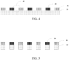
- a method of manufacturing a semiconductor device including: providing a layer to be etched 10; forming a patterned first mask layer 20 on the layer to be etched 10; forming a patterned second mask layer 30 on the layer to be etched 10, where the second mask layer 30 and the first mask layer 20 jointly define openings 40, which exposes the layer to be etched 10; and etching the layer to be etched 10 using the first mask layer 20 and the second mask layer 30 as masks, thus forming a pattern to be etched.
- the above-described method of manufacturing the semiconductor device allows the feature size of the first mask layer 20 and the second mask layer 30 to be relatively larger while keeping the device feature size the same, makes it possible to further reduce the feature size of the device, and can also improve the yield of the device and save costs.
- S10 providing a layer to be etched10, as illustrated in FIG. 2 .
- the method of forming the first mask layer 20 includes a chemical vapor deposition process or an atomic layer deposition process.
- the material of the first mask layer 20 includes one or more selected from the following materials: silicon oxide, silicon nitride, silicon carbide, silicon oxynitride, amorphous carbon, polysilicon, hafnium oxide, titanium oxide, zirconium oxide, titanium nitride, tantalum nitride, and titanium.
- the method of forming the second mask layer 30 includes a chemical vapor deposition process or an atomic layer deposition process.
- the material of the second mask layer 30 includes one or more selected from the following materials: silicon oxide, silicon nitride, silicon carbide, silicon oxynitride, amorphous carbon, polysilicon, hafnium oxide, titanium oxide, zirconium oxide, titanium nitride, tantalum nitride, and titanium.
- the material of the first mask layer 20 is different from the material of the second mask layer 30, and a large etching selection ratio is required.
- the operation of forming a dielectric layer on the first mask layer 20 there is further included the operation of forming a dielectric layer on the first mask layer 20. That is, after the dielectric layer is formed on the first mask layer 20, the second mask layer 30 may be formed on the dielectric layer. At this time, the first mask layer 20 and the second mask layer 30 do not lie on the same plane.
- the material of the dielectric layer is different from the material of the first mask layer 20 and the material of the second mask layer 30 and requires a large etching selection ratio, where the material of the first mask layer 20 may be the same as that of the second mask layer 30.
- the method of forming the dielectric layer includes a chemical vapor deposition process or an atomic layer deposition process.
- the material of the dielectric layer includes one or more selected from the following materials: silicon oxide, silicon nitride, silicon carbide, silicon oxynitride, amorphous carbon, polysilicon, hafnium oxide, titanium oxide, zirconium oxide, titanium nitride, tantalum nitride, and titanium.
- the opening 40 includes a bit line contact hole.
- the first mask layer 20 includes a plurality of first strip masks 201 parallel to each other
- the second mask layer 30 includes a plurality of second strip masks 301 parallel to each other.
- the plurality of first strip masks 201 and the plurality of second strip masks 301 are alternately arranged in side by side.
- the plurality of first strip masks 201 are arranged equidistantly, and the plurality of second strip masks 301 are arranged equidistantly.
- At least one side of the first strip mask 201 is provided with recesses 50 arranged at equal intervals
- at least one side of the second strip mask 301 is provided with recesses 50 arranged at equal intervals.
- the recess 50 of the first strip mask 201 and the second strip mask 301 jointly define openings 40.
- the recess 50 of the second strip mask 301 and the first strip mask 201 jointly define openings 40.
- one side of the first strip mask 201 and one side of the second strip mask 301 are provided with equidistantly arranged recesses 50.
- the recess 50 of the first strip mask 201 and the recess 50 of the second strip mask 301 define an opening 40, as illustrated in FIGS. 8a, 8b , and 8c .
- both sides of the first strip mask 201 and both sides of the second strip mask 301 are provided with recesses 50 arranged at equal intervals.
- the recess 50 of the first strip mask 201 and the recess 50 of the second strip mask 301 define openings 40, as illustrated in FIGS. 6a, 6b , and 6c .
- both sides of the first strip mask 201 or the second strip mask 301 are provided with equidistantly arranged recesses 50, and the recess 50 of the first strip mask 201 and the second strip mask 301 jointly define an openings 40, or the recess 50 of the second strip mask 301 and the first strip mask 201 jointly define openings 40, as shown in FIGS. 7a , 7b, and 7c .
- the shape of the recess 50 includes a triangle, an arc, or a rectangle.
- the shape of the recess 50 is a triangle, as illustrated in FIGS. 6a, 6b , and 6c .
- the shape of the recess 50 is an arc, as illustrated in FIGS. 10a, 10b , and 10c .
- the shape of the recess 50 is a rectangle, as illustrated in FIGS. 9a , 9b, and 9c .
- the first mask layer 20 includes a plurality of first windows 202
- the second mask layer 30 includes a plurality of second windows 302
- the first mask layer 20 and the second mask layer 30 are arranged in a staggered manner to define the openings 40, as illustrated in FIGS. 11a , 11b, and 11c .
- the first windows 202 are arranged in an array
- the second windows 302 are arranged in an array.
- the shapes of the first windows 202 and the second windows 302 include but are not limited to rectangles.
- a semiconductor device including: a layer to be etched 10; a patterned first mask layer 20 formed on the layer to be etched 10; and a patterned second mask layer 30 formed on the layer 10 to be etched, where the second mask layer 30 and the first mask layer 20 jointly define openings 40 that expose the layer to be etched 10.
- the above-described semiconductor device allows the feature size of the first mask layer 20 and the second mask layer 30 to be relatively larger while keeping the device feature size the same, makes it possible to further reduce the feature size of the device, and can also improve the yield of the device and save costs.
- the material of the first mask layer 20 includes one or more selected from the following materials: silicon oxide, silicon nitride, silicon carbide, silicon oxynitride, amorphous carbon, polysilicon, hafnium oxide, titanium oxide, zirconium oxide, titanium nitride, tantalum nitride, and titanium.
- the material of the second mask layer 30 includes one or more selected from the following materials: silicon oxide, silicon nitride, silicon carbide, silicon oxynitride, amorphous carbon, polysilicon, hafnium oxide, titanium oxide, zirconium oxide, titanium nitride, tantalum nitride, and titanium.
- the material of the first mask layer 20 is different from the material of the second mask layer 30, and a large etching selection ratio is required.
- a dielectric layer is further disposed between the first mask layer 20 and the second mask layer 30.
- the material of the dielectric layer is different from the material of the first mask layer 20 and the material of the second mask layer 30 and requires a large etching selection ratio.
- the material of the dielectric layer includes one or more selected from the following materials: silicon oxide, silicon nitride, silicon carbide, silicon oxynitride, amorphous carbon, polysilicon, hafnium oxide, titanium oxide, zirconium oxide, titanium nitride, tantalum nitride, and titanium.
- the opening 40 includes a bit line contact hole.
- the first mask layer 20 includes a plurality of first strip masks 201 parallel to each other
- the second mask layer 30 includes a plurality of second strip masks 301 parallel to each other.
- the plurality of first strip masks 201 and the plurality of second strip masks 301 are alternately arranged in side by side.
- the plurality of first strip masks 201 are arranged equidistantly, and the plurality of second strip masks 301 are arranged equidistantly.
- At least one side of the first strip mask 201 is provided with recesses 50 arranged at equal intervals
- at least one side of the second strip mask 301 is provided with recesses 50 arranged at equal intervals.
- the recess 50 of the first strip mask 201 and the second strip mask 301 jointly define openings 40.
- the recess 50 of the second strip mask 301 and the first strip mask 201 jointly define openings 40.
- one side of the first strip mask 201 and one side of the second strip mask 301 are provided with equidistantly arranged recesses 50.
- the recess 50 of the first strip mask 201 and the recess 50 of the second strip mask 301 define openings 40, as illustrated in FIGS. 8a, 8b , and 8c .
- both sides of the first strip mask 201 and both sides of the second strip mask 301 are provided with recesses 50 arranged at equal intervals.
- the recess 50 of the first strip mask 201 and the recess 50 of the second strip mask 301 define openings 40, as illustrated in FIGS. 6a, 6b , and 6c .
- both sides of the first strip mask 201 or the second strip mask 301 are provided with equidistantly arranged recesses 50, and the recess 50 of the first strip mask 201 and the second strip mask 301 jointly define openings 40, or the recess 50 of the second strip mask 301 and the first strip mask 201 jointly define openings 40, as shown in FIGS. 7a , 7b, and 7c .
- the shape of the recess 50 includes a triangle, an arc, or a rectangle.
- the shape of the recess 50 is a triangle, as illustrated in FIGS. 6a, 6b , and 6c .
- the shape of the recess 50 is an arc, as illustrated in FIGS. 10a, 10b , and 10c .
- the shape of the recess 50 is a rectangle, as illustrated in FIGS. 9a , 9b, and 9c .
- the first mask layer 20 includes a plurality of first windows 202
- the second mask layer 30 includes a plurality of second windows 302
- the first mask layer 20 and the second mask layer 30 are arranged in a staggered manner to define the openings 40, as illustrated in FIGS. 11a , 11b, and 11c .
- the first windows 202 are arranged in an array
- the second windows 302 are arranged in an array.
- the shapes of the first windows 202 and the second windows 302 include but are not limited to rectangles.
- the order of the formation of the first mask layer 20 and the second mask layer 30 as well as the positions where they are formed in the above embodiments can be interchanged.
- the layout direction of the opening 40 relative to the layer to be etched 10 can be adjusted arbitrarily as required.
- the layout directions of the first mask layer 20 and the second mask layer 30 relative to the layer to be etched 10 can be adjusted arbitrarily as required. The above should all be regarded as fall in the scope of this specification.
Landscapes
- Engineering & Computer Science (AREA)
- Manufacturing & Machinery (AREA)
- Semiconductor Memories (AREA)
- Internal Circuitry In Semiconductor Integrated Circuit Devices (AREA)
Abstract
Description
- The present disclosure claims the priority to
Chinese Patent Application No.2019111347757, entitled "Semiconductor Device and Method of Manufacturing the Same" and filed on November 19, 2019 - The present disclosure relates to the field of semiconductors, and more particularly to a semiconductor device and a method of manufacturing the same.
- In electronics, integrated circuit (IC), also referred to as microcircuit, microchip, or chip, is a method of miniaturizing circuits (mainly including semiconductor devices, but also passive components, etc.), and is usually manufactured on the surface of a semiconductor wafer. For example, DRAM (Dynamic Random Access Memory), that is, a dynamic random access memory chip, is the most common memory chip. Over the years, DRAM has continued to develop towards smaller dimensions, allowing more circuits to be packaged per chip. This increases the capacity per unit area, which can reduce costs and increase functionality.
- The disclosure provides a semiconductor device and a method of manufacturing the same.
- The present disclosure provides a method of manufacturing a semiconductor device, the method including: providing a layer to be etched; forming a patterned first mask layer on the layer to be etched; and forming a patterned second mask layer on the layer to be etched, the second mask layer and the first mask layer jointly defining openings to expose the layer to be etched; and etching the layer to be etched using the first mask layer and the second mask layer as masks so as to form a pattern to be etched.
- The present disclosure further provides a semiconductor device including: a layer to be etched; a patterned first mask layer, formed on the layer to be etched; and a patterned second mask layer, formed on the layer to be etched, the second mask layer and the first mask layer jointly define openings to expose the layer to be etched.
- Details of one or more embodiments of this disclosure are set forth in the following drawings and description. Other features and advantages of this disclosure will become apparent from the description, drawings and claims.
- In order to provide a better understanding for the technical solutions portrayed in the embodiments of the present disclosure, the following will briefly introduce the drawings that are needed in the embodiments. Apparently, the drawings in the following description merely illustrate some embodiments of the present disclosure. A person of ordinary skill in the art will be able to obtain other drawings based on these drawings without investing creative efforts.
-
FIG. 1 is a flowchart illustrating a method for manufacturing a semiconductor device according to the present disclosure. -
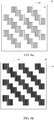
FIGS. 2 to 5 are schematic diagrams illustrating the structure presented in each step of the method of manufacturing the semiconductor device according to the present disclosure. -
FIG. 6a is a top view of a first mask layer in the semiconductor device according to an embodiment of the present disclosure. -
FIG. 6b is a top view of a second mask layer in the semiconductor device according to an embodiment of the present disclosure. -
FIG. 6c is a top view of the first mask layer and the second mask layer in the semiconductor device according to an embodiment of the present disclosure. -
FIG. 7a is a top view of a first mask layer in a semiconductor device according to another embodiment of the present disclosure. -
FIG. 7b is a top view of a second mask layer in the semiconductor device according to another embodiment of the present disclosure. -
FIG. 7c is a top view of the first mask layer and the second mask layer in the semiconductor device according to another embodiment of the present disclosure. -
FIG. 8a is a top view of a first mask layer in a semiconductor device according to yet another embodiment of the present disclosure. -
FIG. 8b is a top view of a second mask layer in the semiconductor device according to yet another embodiment of the present disclosure. -
FIG. 8c is a top view of the first mask layer and the second mask layer in the semiconductor device according to yet another embodiment of the present disclosure. -
FIG. 9a is a top view of a first mask layer in a semiconductor device according to still another embodiment of the present disclosure. -
FIG. 9b is a top view of a second mask layer in the semiconductor device according to still another embodiment of the present disclosure. -
FIG. 9c is a top view of the first mask layer and the second mask layer in the semiconductor device according to still another embodiment of the present disclosure. -
FIG. 10a is a top view of a first mask layer in a semiconductor device according to still another embodiment of the present disclosure. -
FIG. 10b is a top view of a second mask layer in the semiconductor device according to still another embodiment of the present disclosure. -
FIG. 10c is a top view of the first mask layer and the second mask layer in the semiconductor device according to still another embodiment of the present disclosure. -
FIG. 11a is a top view of a first mask layer in a semiconductor device according to still another embodiment of the present disclosure. -
FIG. 11b is a top view of a second mask layer in the semiconductor device according to still another embodiment of the present disclosure. -
FIG. 11c is a top view of the first mask layer and the second mask layer in the semiconductor device according to still another embodiment of the present disclosure. - As mentioned in the Background section, DRAM continues to develop toward smaller dimensions, which requires continuous reduction of the minimum line width and spacing of integrated circuit design. However, when the feature size of the exposure lines approaches the theoretical resolution limit of the exposure system, the imaging on the surface of the silicon wafer will be severely distorted, resulting in a serious degradation of the quality of the photolithography image.
- In order to facilitate the understanding of the present disclosure, the present disclosure will be described in greater detail below with reference to the related drawings. The preferred embodiments according to this disclosure are illustrated in the drawings. However, the present disclosure can be practiced in many different forms and thus will not be limited to the embodiments described herein. On the contrary, the purpose of providing these embodiments is to make the present disclosure more thorough and comprehensive.
- Unless otherwise defined, all technical and scientific terms used herein have the same meaning as commonly understood by those skilled in the technical field to which the present disclosure pertains. The terms used in the specification of the present disclosure herein are intended for mere purposes of describing some specific embodiments, and are not intended to limit the present disclosure by any means or forms. The term "and/or" as used herein is intended to include any and all combinations of one or more related listed items.
- In the description of the present disclosure, it should be understood that terms "upper", "lower", "vertical", "horizontal", "inner", "outer", etc. are used to indicate the orientational or positional relationships based on those depicted in the drawings, which are merely intended for the sake of convenience of describing the present disclosure and simplifying the description, rather than indicating or implying that the device or element referred to must have a specific orientation, or be constructed and operated in a specific orientation, and therefore are not to be understood as restricting the present disclosure.
- In an embodiment, as illustrated in
FIG. 1 , there is provided a method of manufacturing a semiconductor device, the method including: providing a layer to be etched 10; forming a patternedfirst mask layer 20 on the layer to be etched 10; forming a patternedsecond mask layer 30 on the layer to be etched 10, where thesecond mask layer 30 and thefirst mask layer 20 jointly defineopenings 40, which exposes the layer to be etched 10; and etching the layer to be etched 10 using thefirst mask layer 20 and thesecond mask layer 30 as masks, thus forming a pattern to be etched. - In this embodiment, the above-described method of manufacturing the semiconductor device allows the feature size of the
first mask layer 20 and thesecond mask layer 30 to be relatively larger while keeping the device feature size the same, makes it possible to further reduce the feature size of the device, and can also improve the yield of the device and save costs. - S10: providing a layer to be etched10, as illustrated in
FIG. 2 . - S20: forming a patterned
first mask layer 20 on the layer to be etched 10, as illustrated inFIG. 3 . - In one embodiment, the method of forming the
first mask layer 20 includes a chemical vapor deposition process or an atomic layer deposition process. The material of thefirst mask layer 20 includes one or more selected from the following materials: silicon oxide, silicon nitride, silicon carbide, silicon oxynitride, amorphous carbon, polysilicon, hafnium oxide, titanium oxide, zirconium oxide, titanium nitride, tantalum nitride, and titanium. - S30: forming a patterned
second mask layer 30 on the layer to be etched 10, where thesecond mask layer 30 and thefirst mask layer 20 jointly defineopenings 40, which exposes the layer to be etched 10, as illustrated inFIG. 4 . - In one embodiment, the method of forming the
second mask layer 30 includes a chemical vapor deposition process or an atomic layer deposition process. The material of thesecond mask layer 30 includes one or more selected from the following materials: silicon oxide, silicon nitride, silicon carbide, silicon oxynitride, amorphous carbon, polysilicon, hafnium oxide, titanium oxide, zirconium oxide, titanium nitride, tantalum nitride, and titanium. - S40: etching the layer to be etched 10 using the
first mask layer 20 and thesecond mask layer 30 as masks thus forming a pattern to be etched, as illustrated inFIG. 5 . - In this embodiment, the material of the
first mask layer 20 is different from the material of thesecond mask layer 30, and a large etching selection ratio is required. - In another embodiment, between S20 and S30 there is further included the operation of forming a dielectric layer on the
first mask layer 20. That is, after the dielectric layer is formed on thefirst mask layer 20, thesecond mask layer 30 may be formed on the dielectric layer. At this time, thefirst mask layer 20 and thesecond mask layer 30 do not lie on the same plane. The material of the dielectric layer is different from the material of thefirst mask layer 20 and the material of thesecond mask layer 30 and requires a large etching selection ratio, where the material of thefirst mask layer 20 may be the same as that of thesecond mask layer 30. - In one embodiment, the method of forming the dielectric layer includes a chemical vapor deposition process or an atomic layer deposition process. The material of the dielectric layer includes one or more selected from the following materials: silicon oxide, silicon nitride, silicon carbide, silicon oxynitride, amorphous carbon, polysilicon, hafnium oxide, titanium oxide, zirconium oxide, titanium nitride, tantalum nitride, and titanium.
- In one embodiment, the
opening 40 includes a bit line contact hole. - In one embodiment, the
first mask layer 20 includes a plurality of first strip masks 201 parallel to each other, and thesecond mask layer 30 includes a plurality of second strip masks 301 parallel to each other. The plurality of first strip masks 201 and the plurality of second strip masks 301 are alternately arranged in side by side. - In this embodiment, the plurality of first strip masks 201 are arranged equidistantly, and the plurality of second strip masks 301 are arranged equidistantly.
- In one embodiment, at least one side of the
first strip mask 201 is provided withrecesses 50 arranged at equal intervals, and at least one side of thesecond strip mask 301 is provided withrecesses 50 arranged at equal intervals. Therecess 50 of thefirst strip mask 201 and thesecond strip mask 301 jointly defineopenings 40. Therecess 50 of thesecond strip mask 301 and thefirst strip mask 201 jointly defineopenings 40. For example, one side of thefirst strip mask 201 and one side of thesecond strip mask 301 are provided with equidistantly arranged recesses 50. Therecess 50 of thefirst strip mask 201 and therecess 50 of thesecond strip mask 301 define anopening 40, as illustrated inFIGS. 8a, 8b , and8c . - In one embodiment, both sides of the
first strip mask 201 and both sides of thesecond strip mask 301 are provided withrecesses 50 arranged at equal intervals. Therecess 50 of thefirst strip mask 201 and therecess 50 of thesecond strip mask 301 defineopenings 40, as illustrated inFIGS. 6a, 6b , and6c . - In one embodiment, both sides of the
first strip mask 201 or thesecond strip mask 301 are provided with equidistantly arranged recesses 50, and therecess 50 of thefirst strip mask 201 and thesecond strip mask 301 jointly define anopenings 40, or therecess 50 of thesecond strip mask 301 and thefirst strip mask 201 jointly defineopenings 40, as shown inFIGS. 7a ,7b, and 7c . - In one embodiment, the shape of the
recess 50 includes a triangle, an arc, or a rectangle. - In one of the embodiments, the shape of the
recess 50 is a triangle, as illustrated inFIGS. 6a, 6b , and6c . - In one of the embodiments, the shape of the
recess 50 is an arc, as illustrated inFIGS. 10a, 10b , and10c . - In one of the embodiments, the shape of the
recess 50 is a rectangle, as illustrated inFIGS. 9a ,9b, and 9c . - In one embodiment, the
first mask layer 20 includes a plurality offirst windows 202, thesecond mask layer 30 includes a plurality ofsecond windows 302, and thefirst mask layer 20 and thesecond mask layer 30 are arranged in a staggered manner to define theopenings 40, as illustrated inFIGS. 11a ,11b, and 11c . - In this embodiment, the
first windows 202 are arranged in an array, and thesecond windows 302 are arranged in an array. The shapes of thefirst windows 202 and thesecond windows 302 include but are not limited to rectangles. - In an embodiment, as illustrated in
FIG. 4 , there is provided a semiconductor device including: a layer to be etched 10; a patternedfirst mask layer 20 formed on the layer to be etched 10; and a patternedsecond mask layer 30 formed on thelayer 10 to be etched, where thesecond mask layer 30 and thefirst mask layer 20 jointly defineopenings 40 that expose the layer to be etched 10. - In this embodiment, the above-described semiconductor device allows the feature size of the
first mask layer 20 and thesecond mask layer 30 to be relatively larger while keeping the device feature size the same, makes it possible to further reduce the feature size of the device, and can also improve the yield of the device and save costs. - In one embodiment, the material of the
first mask layer 20 includes one or more selected from the following materials: silicon oxide, silicon nitride, silicon carbide, silicon oxynitride, amorphous carbon, polysilicon, hafnium oxide, titanium oxide, zirconium oxide, titanium nitride, tantalum nitride, and titanium. - In one embodiment, the material of the
second mask layer 30 includes one or more selected from the following materials: silicon oxide, silicon nitride, silicon carbide, silicon oxynitride, amorphous carbon, polysilicon, hafnium oxide, titanium oxide, zirconium oxide, titanium nitride, tantalum nitride, and titanium. - In this embodiment, the material of the
first mask layer 20 is different from the material of thesecond mask layer 30, and a large etching selection ratio is required. - In another embodiment, a dielectric layer is further disposed between the
first mask layer 20 and thesecond mask layer 30. The material of the dielectric layer is different from the material of thefirst mask layer 20 and the material of thesecond mask layer 30 and requires a large etching selection ratio. - In one embodiment, the material of the dielectric layer includes one or more selected from the following materials: silicon oxide, silicon nitride, silicon carbide, silicon oxynitride, amorphous carbon, polysilicon, hafnium oxide, titanium oxide, zirconium oxide, titanium nitride, tantalum nitride, and titanium.
- In one embodiment, the
opening 40 includes a bit line contact hole. - In one embodiment, the
first mask layer 20 includes a plurality of first strip masks 201 parallel to each other, and thesecond mask layer 30 includes a plurality of second strip masks 301 parallel to each other. The plurality of first strip masks 201 and the plurality of second strip masks 301 are alternately arranged in side by side. - In this embodiment, the plurality of first strip masks 201 are arranged equidistantly, and the plurality of second strip masks 301 are arranged equidistantly.
- In one embodiment, at least one side of the
first strip mask 201 is provided withrecesses 50 arranged at equal intervals, and at least one side of thesecond strip mask 301 is provided withrecesses 50 arranged at equal intervals. Therecess 50 of thefirst strip mask 201 and thesecond strip mask 301 jointly defineopenings 40. Therecess 50 of thesecond strip mask 301 and thefirst strip mask 201 jointly defineopenings 40. For example, one side of thefirst strip mask 201 and one side of thesecond strip mask 301 are provided with equidistantly arranged recesses 50. Therecess 50 of thefirst strip mask 201 and therecess 50 of thesecond strip mask 301 defineopenings 40, as illustrated inFIGS. 8a, 8b , and8c . - In one embodiment, both sides of the
first strip mask 201 and both sides of thesecond strip mask 301 are provided withrecesses 50 arranged at equal intervals. Therecess 50 of thefirst strip mask 201 and therecess 50 of thesecond strip mask 301 defineopenings 40, as illustrated inFIGS. 6a, 6b , and6c . - In one embodiment, both sides of the
first strip mask 201 or thesecond strip mask 301 are provided with equidistantly arranged recesses 50, and therecess 50 of thefirst strip mask 201 and thesecond strip mask 301 jointly defineopenings 40, or therecess 50 of thesecond strip mask 301 and thefirst strip mask 201 jointly defineopenings 40, as shown inFIGS. 7a ,7b, and 7c . - In one embodiment, the shape of the
recess 50 includes a triangle, an arc, or a rectangle. - In one of the embodiments, the shape of the
recess 50 is a triangle, as illustrated inFIGS. 6a, 6b , and6c . - In one of the embodiments, the shape of the
recess 50 is an arc, as illustrated inFIGS. 10a, 10b , and10c . - In one of the embodiments, the shape of the
recess 50 is a rectangle, as illustrated inFIGS. 9a ,9b, and 9c . - In one embodiment, the
first mask layer 20 includes a plurality offirst windows 202, thesecond mask layer 30 includes a plurality ofsecond windows 302, and thefirst mask layer 20 and thesecond mask layer 30 are arranged in a staggered manner to define theopenings 40, as illustrated inFIGS. 11a ,11b, and 11c . - In this embodiment, the
first windows 202 are arranged in an array, and thesecond windows 302 are arranged in an array. The shapes of thefirst windows 202 and thesecond windows 302 include but are not limited to rectangles. - The order of the formation of the
first mask layer 20 and thesecond mask layer 30 as well as the positions where they are formed in the above embodiments can be interchanged. The layout direction of theopening 40 relative to the layer to be etched 10 can be adjusted arbitrarily as required. The layout directions of thefirst mask layer 20 and thesecond mask layer 30 relative to the layer to be etched 10 can be adjusted arbitrarily as required. The above should all be regarded as fall in the scope of this specification. - The technical features of the above embodiments can be combined in any desirable manner. For the sake of conciseness, all possible combinations of the technical features in the above embodiments are not to be and cannot be exhausted. However, as long as no contradiction or conflict is present in the combination of these technical features, they are all to be regarded as fall in the range of this specification.
- The foregoing embodiments merely illustrate some specific implementations according to the present disclosure in a relatively specific and detailed manner, but it should not be understood as a limitation on the scope of protection of the present disclosure. It should be pointed out that for those having ordinary skill in the art, numerous modifications and improvements can be made without departing from the concept and spirit of the present disclosure and these shall all fall in the scope of protection of the present disclosure. Therefore, the scope of protection of the present disclosure should be defined in and by the appended claims.
| 10 | Layer to be etched |
| 20 | |
| 201 | |
| 202 | |
| 30 | |
| 301 | |
| 302 | |
| 40 | |
| 50 | Recess |
Claims (16)
- A method of manufacturing a semiconductor device, comprising:providing a layer to be etched;forming a patterned first mask layer on the layer to be etched;forming a patterned second mask layer on the layer to be etched, the second mask layer and the first mask layer jointly defining openings to expose the layer to be etched; andetching the layer to be etched using the first mask layer and the second mask layer as masks so as to form a pattern to be etched.
- The method of claim 1, wherein the first mask layer comprises a plurality of first strip masks disposed parallel to each other, and the second mask layer comprises a plurality of second strip masks disposed parallel to each other, wherein the plurality of first strip masks and the plurality of second strip masks are alternately disposed in parallel.
- The method of claim 2, wherein at least one side of the first strip mask comprises recesses that are arranged at equal intervals, and at least one side of the second strip mask comprises recesses that are arranged at equal intervals, wherein the recesses of the first strip mask and the second strip mask jointly define the openings, and the recesses of the second strip mask and the first strip mask jointly define the openings.
- The method of claim 3, wherein both sides of the first strip mask comprise the recesses that are provided at equal intervals, both sides of the second strip mask comprise the recesses that are provided at equal intervals, wherein the recesses of the first strip mask and the recesses of the second strip mask jointly define the openings.
- The method of claim 2, wherein both sides of the first strip mask or both sides of the second strip mask comprise recesses that are arranged at equal intervals, wherein the recesses of the first strip mask and the second strip mask jointly define the openings, or the recesses of the second strip mask and the first strip mask jointly define the openings.
- The method of any one of claims 3 to 5, wherein a shape of the recesses comprises a triangle, an arc, or a rectangle.
- The method of claim 1, wherein the first mask layer comprises a plurality of first windows, the second mask layer comprises a plurality of second windows, wherein the first mask layer and the second mask layer are arranged in a staggered manner to form the openings.
- The method of claim 1, after forming the first mask layer, the method further comprises forming a dielectric layer on the first mask layer.
- A semiconductor device, comprising:a layer to be etched;a patterned first mask layer, formed on the layer to be etched; anda patterned second mask layer, formed on the layer to be etched, wherein the second mask layer and the first mask layer jointly define openings to expose the layer to be etched.
- The semiconductor device of claim 9, wherein the first mask layer comprises a plurality of first strip masks disposed parallel to each other, and the second mask layer comprises a plurality of second strip masks disposed parallel to each other, and wherein the plurality of first strip masks and the plurality of second strip masks are alternately disposed in parallel.
- The semiconductor device of claim 10, wherein at least one side of the first strip mask comprises recesses that are arranged at equal intervals, and at least one side of the second strip mask comprises recesses that are arranged at equal intervals, wherein the recesses of the first strip mask and the second strip mask jointly define the openings, and the recesses of the second strip mask and the first strip mask jointly define the openings.
- The semiconductor device of claim 11, wherein both sides of the first strip mask comprise the recesses that are provided at equal intervals, both sides of the second strip mask comprise the recesses that are provided at equal intervals, wherein the recesses of the first strip mask and the recesses of the second strip mask jointly define the openings.
- The semiconductor device of claim 10, wherein both sides of a first strip mask or both sides of a second strip mask comprise recesses that are arranged at equal intervals, wherein the recesses of the first strip mask and the second strip mask jointly define the openings, or the recesses of the second strip mask and the first strip mask jointly define the openings.
- The semiconductor device of any one of claims 11 to 13, wherein a shape of the recesses comprises a triangle, an arc, or a rectangle.
- The semiconductor device of claim 9, wherein the first mask layer comprises a plurality of first windows, the second mask layer comprises a plurality of second windows, wherein the first mask layer and the second mask layer are arranged in a staggered manner to form the openings.
- The semiconductor device of claim 9, further comprising a dielectric layer, disposed between the first mask layer and the second mask layer.
Applications Claiming Priority (2)
| Application Number | Priority Date | Filing Date | Title |
|---|---|---|---|
| CN201911134775.7A CN112908837B (en) | 2019-11-19 | 2019-11-19 | Semiconductor device and method for manufacturing semiconductor device |
| PCT/CN2020/111399 WO2021098324A1 (en) | 2019-11-19 | 2020-08-26 | Semiconductor device and manufacturing method of semiconductor device |
Publications (3)
| Publication Number | Publication Date |
|---|---|
| EP3933887A1 true EP3933887A1 (en) | 2022-01-05 |
| EP3933887A4 EP3933887A4 (en) | 2022-06-29 |
| EP3933887B1 EP3933887B1 (en) | 2024-01-31 |
Family
ID=75980281
Family Applications (1)
| Application Number | Title | Priority Date | Filing Date |
|---|---|---|---|
| EP20891144.6A Active EP3933887B1 (en) | 2019-11-19 | 2020-08-26 | Semiconductor device and manufacturing method of semiconductor device |
Country Status (4)
| Country | Link |
|---|---|
| US (1) | US11990340B2 (en) |
| EP (1) | EP3933887B1 (en) |
| CN (1) | CN112908837B (en) |
| WO (1) | WO2021098324A1 (en) |
Families Citing this family (2)
| Publication number | Priority date | Publication date | Assignee | Title |
|---|---|---|---|---|
| CN113628957B (en) * | 2021-08-05 | 2023-10-10 | 长鑫存储技术有限公司 | Patterning methods and semiconductor structures |
| CN115000294B (en) * | 2022-05-25 | 2026-04-14 | 长鑫存储技术有限公司 | Method for preparing semiconductor structure, semiconductor structure and memory |
Family Cites Families (20)
| Publication number | Priority date | Publication date | Assignee | Title |
|---|---|---|---|---|
| US6664011B2 (en) * | 2001-12-05 | 2003-12-16 | Taiwan Semiconductor Manufacturing Company | Hole printing by packing and unpacking using alternating phase-shifting masks |
| KR100674970B1 (en) * | 2005-04-21 | 2007-01-26 | 삼성전자주식회사 | Fine pitch pattern formation method using double spacers |
| JP2009194196A (en) * | 2008-02-15 | 2009-08-27 | Nec Electronics Corp | Semiconductor device manufacturing method and semiconductor device |
| US8173549B2 (en) * | 2008-06-03 | 2012-05-08 | Samsung Electronics Co., Ltd. | Methods of forming semiconductor device patterns |
| KR101096218B1 (en) * | 2009-10-30 | 2011-12-22 | 주식회사 하이닉스반도체 | Method for manufacturing semiconductor device |
| KR101087835B1 (en) * | 2009-11-26 | 2011-11-30 | 주식회사 하이닉스반도체 | Method of forming fine pattern of semiconductor device |
| KR20120074902A (en) * | 2010-12-28 | 2012-07-06 | 에스케이하이닉스 주식회사 | Method for forming patterns in the semiconductor devices |
| CN102881566B (en) * | 2012-09-27 | 2017-07-25 | 上海集成电路研发中心有限公司 | A kind of forming method of via hole image |
| CN103911584B (en) * | 2012-12-31 | 2017-07-04 | 上海天马微电子有限公司 | Mask plate |
| WO2014148423A1 (en) * | 2013-03-21 | 2014-09-25 | ピーエスフォー ルクスコ エスエイアールエル | Semiconductor device and method for producing same |
| CN104681429B (en) * | 2013-11-27 | 2017-12-29 | 中芯国际集成电路制造(上海)有限公司 | The forming method of semiconductor structure |
| CN103984202A (en) * | 2014-04-23 | 2014-08-13 | 京东方科技集团股份有限公司 | Masking plate and color film substrate manufacturing method |
| KR20160005945A (en) * | 2014-07-08 | 2016-01-18 | 에스케이하이닉스 주식회사 | Mask pattern and method for forming fine patterns of a semiconductor device |
| KR102411067B1 (en) * | 2017-05-10 | 2022-06-21 | 삼성전자주식회사 | Method for fabricating three-dimensional semiconductor devices |
| CN109148376B (en) * | 2017-06-28 | 2020-07-31 | 长鑫存储技术有限公司 | Memory and forming method thereof, and semiconductor device |
| TW201917775A (en) * | 2017-07-15 | 2019-05-01 | 美商微材料有限責任公司 | Mask scheme for cut pattern flow with enlarged EPE window |
| CN109935515B (en) * | 2017-12-18 | 2021-07-13 | 联华电子股份有限公司 | method of forming a graph |
| CN108519725B (en) * | 2018-04-20 | 2024-01-23 | 长鑫存储技术有限公司 | Combination mask, semiconductor device and method of forming same |
| CN208922054U (en) * | 2018-10-09 | 2019-05-31 | 长鑫存储技术有限公司 | Masks, capacitor arrays and semiconductor devices |
| CN210575830U (en) * | 2019-11-19 | 2020-05-19 | 长鑫存储技术有限公司 | Semiconductor device |
-
2019
- 2019-11-19 CN CN201911134775.7A patent/CN112908837B/en active Active
-
2020
- 2020-08-26 EP EP20891144.6A patent/EP3933887B1/en active Active
- 2020-08-26 WO PCT/CN2020/111399 patent/WO2021098324A1/en not_active Ceased
-
2021
- 2021-06-08 US US17/342,508 patent/US11990340B2/en active Active
Also Published As
| Publication number | Publication date |
|---|---|
| CN112908837B (en) | 2025-04-11 |
| EP3933887A4 (en) | 2022-06-29 |
| US11990340B2 (en) | 2024-05-21 |
| US20210296126A1 (en) | 2021-09-23 |
| WO2021098324A1 (en) | 2021-05-27 |
| CN112908837A (en) | 2021-06-04 |
| EP3933887B1 (en) | 2024-01-31 |
Similar Documents
| Publication | Publication Date | Title |
|---|---|---|
| US11037789B2 (en) | Cut last self-aligned litho-etch patterning | |
| CN112908968B (en) | Capacitor in semiconductor memory and method for fabricating the same | |
| US9941285B2 (en) | Pattern forming method and semiconductor device manufacturing method using the same | |
| JP5007465B2 (en) | Method for forming capacitor device | |
| US12238920B2 (en) | Semiconductor devices having air spacer | |
| KR102411071B1 (en) | Semiconductor device | |
| US11342333B2 (en) | Semiconductor device | |
| US20250294722A1 (en) | Semiconductor device and manufacturing method | |
| US11990340B2 (en) | Semiconductor device and method of manufacturing the same | |
| US20060181656A1 (en) | Placement configuration of MIM type capacitance element | |
| WO2021258561A1 (en) | Memory forming method and memory | |
| US20240357802A1 (en) | Semiconductor memory devices | |
| CN116801633A (en) | Semiconductor memory device and manufacturing process thereof | |
| CN210575830U (en) | Semiconductor device | |
| CN114068420B (en) | Memory forming method and memory | |
| KR20210047125A (en) | Semiconductor memory devices | |
| KR100644526B1 (en) | Manufacturing method of embossed capacitor | |
| US20050139905A1 (en) | Dummy layer in semiconductor device and fabricating method thereof | |
| US8030697B2 (en) | Cell structure of semiconductor device having an active region with a concave portion | |
| EP0788164A1 (en) | Memory cell configuration for increased capacitor area | |
| US12635126B2 (en) | Semiconductor memory devices including stepwise profiles and methods of fabricating the same | |
| JPH06310671A (en) | Semiconductor device | |
| KR20090095395A (en) | Contact formation method of flash memory device | |
| US20220044964A1 (en) | Semiconductor structure and method for manufacturing same | |
| CN117896980A (en) | Semiconductor device |
Legal Events
| Date | Code | Title | Description |
|---|---|---|---|
| STAA | Information on the status of an ep patent application or granted ep patent |
Free format text: STATUS: THE INTERNATIONAL PUBLICATION HAS BEEN MADE |
|
| PUAI | Public reference made under article 153(3) epc to a published international application that has entered the european phase |
Free format text: ORIGINAL CODE: 0009012 |
|
| STAA | Information on the status of an ep patent application or granted ep patent |
Free format text: STATUS: REQUEST FOR EXAMINATION WAS MADE |
|
| 17P | Request for examination filed |
Effective date: 20210930 |
|
| AK | Designated contracting states |
Kind code of ref document: A1 Designated state(s): AL AT BE BG CH CY CZ DE DK EE ES FI FR GB GR HR HU IE IS IT LI LT LU LV MC MK MT NL NO PL PT RO RS SE SI SK SM TR |
|
| A4 | Supplementary search report drawn up and despatched |
Effective date: 20220601 |
|
| RIC1 | Information provided on ipc code assigned before grant |
Ipc: H01L 27/108 20060101ALI20220525BHEP Ipc: H01L 21/8242 20060101ALI20220525BHEP Ipc: H01L 21/033 20060101AFI20220525BHEP |
|
| DAV | Request for validation of the european patent (deleted) | ||
| DAX | Request for extension of the european patent (deleted) | ||
| STAA | Information on the status of an ep patent application or granted ep patent |
Free format text: STATUS: EXAMINATION IS IN PROGRESS |
|
| 17Q | First examination report despatched |
Effective date: 20230222 |
|
| RIC1 | Information provided on ipc code assigned before grant |
Ipc: H01L 29/66 20060101ALI20230825BHEP Ipc: H01L 21/768 20060101ALI20230825BHEP Ipc: H01L 21/311 20060101ALI20230825BHEP Ipc: H01L 21/033 20060101AFI20230825BHEP |
|
| GRAP | Despatch of communication of intention to grant a patent |
Free format text: ORIGINAL CODE: EPIDOSNIGR1 |
|
| STAA | Information on the status of an ep patent application or granted ep patent |
Free format text: STATUS: GRANT OF PATENT IS INTENDED |
|
| INTG | Intention to grant announced |
Effective date: 20231006 |
|
| GRAS | Grant fee paid |
Free format text: ORIGINAL CODE: EPIDOSNIGR3 |
|
| GRAA | (expected) grant |
Free format text: ORIGINAL CODE: 0009210 |
|
| STAA | Information on the status of an ep patent application or granted ep patent |
Free format text: STATUS: THE PATENT HAS BEEN GRANTED |
|
| AK | Designated contracting states |
Kind code of ref document: B1 Designated state(s): AL AT BE BG CH CY CZ DE DK EE ES FI FR GB GR HR HU IE IS IT LI LT LU LV MC MK MT NL NO PL PT RO RS SE SI SK SM TR |
|
| P01 | Opt-out of the competence of the unified patent court (upc) registered |
Effective date: 20231223 |
|
| REG | Reference to a national code |
Ref country code: GB Ref legal event code: FG4D Ref country code: CH Ref legal event code: EP |
|
| REG | Reference to a national code |
Ref country code: DE Ref legal event code: R096 Ref document number: 602020025193 Country of ref document: DE |
|
| REG | Reference to a national code |
Ref country code: IE Ref legal event code: FG4D |
|
| REG | Reference to a national code |
Ref country code: LT Ref legal event code: MG9D |
|
| REG | Reference to a national code |
Ref country code: NL Ref legal event code: MP Effective date: 20240131 |
|
| PG25 | Lapsed in a contracting state [announced via postgrant information from national office to epo] |
Ref country code: IS Free format text: LAPSE BECAUSE OF FAILURE TO SUBMIT A TRANSLATION OF THE DESCRIPTION OR TO PAY THE FEE WITHIN THE PRESCRIBED TIME-LIMIT Effective date: 20240531 |
|
| PG25 | Lapsed in a contracting state [announced via postgrant information from national office to epo] |
Ref country code: LT Free format text: LAPSE BECAUSE OF FAILURE TO SUBMIT A TRANSLATION OF THE DESCRIPTION OR TO PAY THE FEE WITHIN THE PRESCRIBED TIME-LIMIT Effective date: 20240131 |
|
| PG25 | Lapsed in a contracting state [announced via postgrant information from national office to epo] |
Ref country code: GR Free format text: LAPSE BECAUSE OF FAILURE TO SUBMIT A TRANSLATION OF THE DESCRIPTION OR TO PAY THE FEE WITHIN THE PRESCRIBED TIME-LIMIT Effective date: 20240501 |
|
| REG | Reference to a national code |
Ref country code: AT Ref legal event code: MK05 Ref document number: 1654449 Country of ref document: AT Kind code of ref document: T Effective date: 20240131 |
|
| PG25 | Lapsed in a contracting state [announced via postgrant information from national office to epo] |
Ref country code: HR Free format text: LAPSE BECAUSE OF FAILURE TO SUBMIT A TRANSLATION OF THE DESCRIPTION OR TO PAY THE FEE WITHIN THE PRESCRIBED TIME-LIMIT Effective date: 20240131 Ref country code: NL Free format text: LAPSE BECAUSE OF FAILURE TO SUBMIT A TRANSLATION OF THE DESCRIPTION OR TO PAY THE FEE WITHIN THE PRESCRIBED TIME-LIMIT Effective date: 20240131 |
|
| PG25 | Lapsed in a contracting state [announced via postgrant information from national office to epo] |
Ref country code: ES Free format text: LAPSE BECAUSE OF FAILURE TO SUBMIT A TRANSLATION OF THE DESCRIPTION OR TO PAY THE FEE WITHIN THE PRESCRIBED TIME-LIMIT Effective date: 20240131 |
|
| PG25 | Lapsed in a contracting state [announced via postgrant information from national office to epo] |
Ref country code: AT Free format text: LAPSE BECAUSE OF FAILURE TO SUBMIT A TRANSLATION OF THE DESCRIPTION OR TO PAY THE FEE WITHIN THE PRESCRIBED TIME-LIMIT Effective date: 20240131 |
|
| PG25 | Lapsed in a contracting state [announced via postgrant information from national office to epo] |
Ref country code: NO Free format text: LAPSE BECAUSE OF FAILURE TO SUBMIT A TRANSLATION OF THE DESCRIPTION OR TO PAY THE FEE WITHIN THE PRESCRIBED TIME-LIMIT Effective date: 20240430 Ref country code: NL Free format text: LAPSE BECAUSE OF FAILURE TO SUBMIT A TRANSLATION OF THE DESCRIPTION OR TO PAY THE FEE WITHIN THE PRESCRIBED TIME-LIMIT Effective date: 20240131 Ref country code: LT Free format text: LAPSE BECAUSE OF FAILURE TO SUBMIT A TRANSLATION OF THE DESCRIPTION OR TO PAY THE FEE WITHIN THE PRESCRIBED TIME-LIMIT Effective date: 20240131 Ref country code: IS Free format text: LAPSE BECAUSE OF FAILURE TO SUBMIT A TRANSLATION OF THE DESCRIPTION OR TO PAY THE FEE WITHIN THE PRESCRIBED TIME-LIMIT Effective date: 20240531 Ref country code: HR Free format text: LAPSE BECAUSE OF FAILURE TO SUBMIT A TRANSLATION OF THE DESCRIPTION OR TO PAY THE FEE WITHIN THE PRESCRIBED TIME-LIMIT Effective date: 20240131 Ref country code: GR Free format text: LAPSE BECAUSE OF FAILURE TO SUBMIT A TRANSLATION OF THE DESCRIPTION OR TO PAY THE FEE WITHIN THE PRESCRIBED TIME-LIMIT Effective date: 20240501 Ref country code: FI Free format text: LAPSE BECAUSE OF FAILURE TO SUBMIT A TRANSLATION OF THE DESCRIPTION OR TO PAY THE FEE WITHIN THE PRESCRIBED TIME-LIMIT Effective date: 20240131 Ref country code: ES Free format text: LAPSE BECAUSE OF FAILURE TO SUBMIT A TRANSLATION OF THE DESCRIPTION OR TO PAY THE FEE WITHIN THE PRESCRIBED TIME-LIMIT Effective date: 20240131 Ref country code: BG Free format text: LAPSE BECAUSE OF FAILURE TO SUBMIT A TRANSLATION OF THE DESCRIPTION OR TO PAY THE FEE WITHIN THE PRESCRIBED TIME-LIMIT Effective date: 20240131 Ref country code: AT Free format text: LAPSE BECAUSE OF FAILURE TO SUBMIT A TRANSLATION OF THE DESCRIPTION OR TO PAY THE FEE WITHIN THE PRESCRIBED TIME-LIMIT Effective date: 20240131 |
|
| PG25 | Lapsed in a contracting state [announced via postgrant information from national office to epo] |
Ref country code: PT Free format text: LAPSE BECAUSE OF FAILURE TO SUBMIT A TRANSLATION OF THE DESCRIPTION OR TO PAY THE FEE WITHIN THE PRESCRIBED TIME-LIMIT Effective date: 20240531 Ref country code: PL Free format text: LAPSE BECAUSE OF FAILURE TO SUBMIT A TRANSLATION OF THE DESCRIPTION OR TO PAY THE FEE WITHIN THE PRESCRIBED TIME-LIMIT Effective date: 20240131 |
|
| PG25 | Lapsed in a contracting state [announced via postgrant information from national office to epo] |
Ref country code: SE Free format text: LAPSE BECAUSE OF FAILURE TO SUBMIT A TRANSLATION OF THE DESCRIPTION OR TO PAY THE FEE WITHIN THE PRESCRIBED TIME-LIMIT Effective date: 20240131 Ref country code: PT Free format text: LAPSE BECAUSE OF FAILURE TO SUBMIT A TRANSLATION OF THE DESCRIPTION OR TO PAY THE FEE WITHIN THE PRESCRIBED TIME-LIMIT Effective date: 20240531 Ref country code: PL Free format text: LAPSE BECAUSE OF FAILURE TO SUBMIT A TRANSLATION OF THE DESCRIPTION OR TO PAY THE FEE WITHIN THE PRESCRIBED TIME-LIMIT Effective date: 20240131 Ref country code: LV Free format text: LAPSE BECAUSE OF FAILURE TO SUBMIT A TRANSLATION OF THE DESCRIPTION OR TO PAY THE FEE WITHIN THE PRESCRIBED TIME-LIMIT Effective date: 20240131 |
|
| PG25 | Lapsed in a contracting state [announced via postgrant information from national office to epo] |
Ref country code: DK Free format text: LAPSE BECAUSE OF FAILURE TO SUBMIT A TRANSLATION OF THE DESCRIPTION OR TO PAY THE FEE WITHIN THE PRESCRIBED TIME-LIMIT Effective date: 20240131 |
|
| PG25 | Lapsed in a contracting state [announced via postgrant information from national office to epo] |
Ref country code: SM Free format text: LAPSE BECAUSE OF FAILURE TO SUBMIT A TRANSLATION OF THE DESCRIPTION OR TO PAY THE FEE WITHIN THE PRESCRIBED TIME-LIMIT Effective date: 20240131 |
|
| PG25 | Lapsed in a contracting state [announced via postgrant information from national office to epo] |
Ref country code: CZ Free format text: LAPSE BECAUSE OF FAILURE TO SUBMIT A TRANSLATION OF THE DESCRIPTION OR TO PAY THE FEE WITHIN THE PRESCRIBED TIME-LIMIT Effective date: 20240131 Ref country code: EE Free format text: LAPSE BECAUSE OF FAILURE TO SUBMIT A TRANSLATION OF THE DESCRIPTION OR TO PAY THE FEE WITHIN THE PRESCRIBED TIME-LIMIT Effective date: 20240131 |
|
| PG25 | Lapsed in a contracting state [announced via postgrant information from national office to epo] |
Ref country code: SK Free format text: LAPSE BECAUSE OF FAILURE TO SUBMIT A TRANSLATION OF THE DESCRIPTION OR TO PAY THE FEE WITHIN THE PRESCRIBED TIME-LIMIT Effective date: 20240131 |
|
| PG25 | Lapsed in a contracting state [announced via postgrant information from national office to epo] |
Ref country code: SM Free format text: LAPSE BECAUSE OF FAILURE TO SUBMIT A TRANSLATION OF THE DESCRIPTION OR TO PAY THE FEE WITHIN THE PRESCRIBED TIME-LIMIT Effective date: 20240131 Ref country code: SK Free format text: LAPSE BECAUSE OF FAILURE TO SUBMIT A TRANSLATION OF THE DESCRIPTION OR TO PAY THE FEE WITHIN THE PRESCRIBED TIME-LIMIT Effective date: 20240131 Ref country code: RO Free format text: LAPSE BECAUSE OF FAILURE TO SUBMIT A TRANSLATION OF THE DESCRIPTION OR TO PAY THE FEE WITHIN THE PRESCRIBED TIME-LIMIT Effective date: 20240131 Ref country code: EE Free format text: LAPSE BECAUSE OF FAILURE TO SUBMIT A TRANSLATION OF THE DESCRIPTION OR TO PAY THE FEE WITHIN THE PRESCRIBED TIME-LIMIT Effective date: 20240131 Ref country code: DK Free format text: LAPSE BECAUSE OF FAILURE TO SUBMIT A TRANSLATION OF THE DESCRIPTION OR TO PAY THE FEE WITHIN THE PRESCRIBED TIME-LIMIT Effective date: 20240131 Ref country code: CZ Free format text: LAPSE BECAUSE OF FAILURE TO SUBMIT A TRANSLATION OF THE DESCRIPTION OR TO PAY THE FEE WITHIN THE PRESCRIBED TIME-LIMIT Effective date: 20240131 |
|
| REG | Reference to a national code |
Ref country code: DE Ref legal event code: R097 Ref document number: 602020025193 Country of ref document: DE |
|
| PG25 | Lapsed in a contracting state [announced via postgrant information from national office to epo] |
Ref country code: IT Free format text: LAPSE BECAUSE OF FAILURE TO SUBMIT A TRANSLATION OF THE DESCRIPTION OR TO PAY THE FEE WITHIN THE PRESCRIBED TIME-LIMIT Effective date: 20240131 |
|
| PLBE | No opposition filed within time limit |
Free format text: ORIGINAL CODE: 0009261 |
|
| STAA | Information on the status of an ep patent application or granted ep patent |
Free format text: STATUS: NO OPPOSITION FILED WITHIN TIME LIMIT |
|
| PG25 | Lapsed in a contracting state [announced via postgrant information from national office to epo] |
Ref country code: IT Free format text: LAPSE BECAUSE OF FAILURE TO SUBMIT A TRANSLATION OF THE DESCRIPTION OR TO PAY THE FEE WITHIN THE PRESCRIBED TIME-LIMIT Effective date: 20240131 |
|
| 26N | No opposition filed |
Effective date: 20241101 |
|
| REG | Reference to a national code |
Ref country code: CH Ref legal event code: PL |
|
| PG25 | Lapsed in a contracting state [announced via postgrant information from national office to epo] |
Ref country code: LU Free format text: LAPSE BECAUSE OF NON-PAYMENT OF DUE FEES Effective date: 20240826 |
|
| GBPC | Gb: european patent ceased through non-payment of renewal fee |
Effective date: 20240826 |
|
| PG25 | Lapsed in a contracting state [announced via postgrant information from national office to epo] |
Ref country code: SI Free format text: LAPSE BECAUSE OF FAILURE TO SUBMIT A TRANSLATION OF THE DESCRIPTION OR TO PAY THE FEE WITHIN THE PRESCRIBED TIME-LIMIT Effective date: 20240131 Ref country code: MC Free format text: LAPSE BECAUSE OF FAILURE TO SUBMIT A TRANSLATION OF THE DESCRIPTION OR TO PAY THE FEE WITHIN THE PRESCRIBED TIME-LIMIT Effective date: 20240131 Ref country code: CH Free format text: LAPSE BECAUSE OF NON-PAYMENT OF DUE FEES Effective date: 20240831 |
|
| PG25 | Lapsed in a contracting state [announced via postgrant information from national office to epo] |
Ref country code: RS Free format text: LAPSE BECAUSE OF FAILURE TO SUBMIT A TRANSLATION OF THE DESCRIPTION OR TO PAY THE FEE WITHIN THE PRESCRIBED TIME-LIMIT Effective date: 20240131 |
|
| REG | Reference to a national code |
Ref country code: BE Ref legal event code: MM Effective date: 20240831 |
|
| PG25 | Lapsed in a contracting state [announced via postgrant information from national office to epo] |
Ref country code: GB Free format text: LAPSE BECAUSE OF NON-PAYMENT OF DUE FEES Effective date: 20240826 |
|
| PG25 | Lapsed in a contracting state [announced via postgrant information from national office to epo] |
Ref country code: BE Free format text: LAPSE BECAUSE OF NON-PAYMENT OF DUE FEES Effective date: 20240831 |
|
| PG25 | Lapsed in a contracting state [announced via postgrant information from national office to epo] |
Ref country code: FR Free format text: LAPSE BECAUSE OF NON-PAYMENT OF DUE FEES Effective date: 20240831 |
|
| PG25 | Lapsed in a contracting state [announced via postgrant information from national office to epo] |
Ref country code: IE Free format text: LAPSE BECAUSE OF NON-PAYMENT OF DUE FEES Effective date: 20240826 |
|
| PGFP | Annual fee paid to national office [announced via postgrant information from national office to epo] |
Ref country code: DE Payment date: 20250820 Year of fee payment: 6 |
|
| REG | Reference to a national code |
Ref country code: DE Ref legal event code: R079 Ref document number: 602020025193 Country of ref document: DE Free format text: PREVIOUS MAIN CLASS: H01L0021033000 Ipc: H10P0076400000 |
|
| PG25 | Lapsed in a contracting state [announced via postgrant information from national office to epo] |
Ref country code: CY Free format text: LAPSE BECAUSE OF FAILURE TO SUBMIT A TRANSLATION OF THE DESCRIPTION OR TO PAY THE FEE WITHIN THE PRESCRIBED TIME-LIMIT; INVALID AB INITIO Effective date: 20200826 |
|
| PG25 | Lapsed in a contracting state [announced via postgrant information from national office to epo] |
Ref country code: HU Free format text: LAPSE BECAUSE OF FAILURE TO SUBMIT A TRANSLATION OF THE DESCRIPTION OR TO PAY THE FEE WITHIN THE PRESCRIBED TIME-LIMIT; INVALID AB INITIO Effective date: 20200826 |