EP3933502A1 - Optical processing apparatus, camera module, electronic device and capturing method - Google Patents
Optical processing apparatus, camera module, electronic device and capturing method Download PDFInfo
- Publication number
- EP3933502A1 EP3933502A1 EP21164818.3A EP21164818A EP3933502A1 EP 3933502 A1 EP3933502 A1 EP 3933502A1 EP 21164818 A EP21164818 A EP 21164818A EP 3933502 A1 EP3933502 A1 EP 3933502A1
- Authority
- EP
- European Patent Office
- Prior art keywords
- light
- optical path
- waveband
- optical
- incident
- Prior art date
- Legal status (The legal status is an assumption and is not a legal conclusion. Google has not performed a legal analysis and makes no representation as to the accuracy of the status listed.)
- Pending
Links
Images

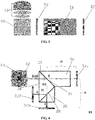


Classifications
-
- G—PHYSICS
- G03—PHOTOGRAPHY; CINEMATOGRAPHY; ANALOGOUS TECHNIQUES USING WAVES OTHER THAN OPTICAL WAVES; ELECTROGRAPHY; HOLOGRAPHY
- G03B—APPARATUS OR ARRANGEMENTS FOR TAKING PHOTOGRAPHS OR FOR PROJECTING OR VIEWING THEM; APPARATUS OR ARRANGEMENTS EMPLOYING ANALOGOUS TECHNIQUES USING WAVES OTHER THAN OPTICAL WAVES; ACCESSORIES THEREFOR
- G03B33/00—Colour photography, other than mere exposure or projection of a colour film
-
- G—PHYSICS
- G02—OPTICS
- G02B—OPTICAL ELEMENTS, SYSTEMS OR APPARATUS
- G02B27/00—Optical systems or apparatus not provided for by any of the groups G02B1/00 - G02B26/00, G02B30/00
- G02B27/10—Beam splitting or combining systems
- G02B27/1006—Beam splitting or combining systems for splitting or combining different wavelengths
-
- H—ELECTRICITY
- H04—ELECTRIC COMMUNICATION TECHNIQUE
- H04N—PICTORIAL COMMUNICATION, e.g. TELEVISION
- H04N23/00—Cameras or camera modules comprising electronic image sensors; Control thereof
- H04N23/50—Constructional details
- H04N23/55—Optical parts specially adapted for electronic image sensors; Mounting thereof
-
- G—PHYSICS
- G03—PHOTOGRAPHY; CINEMATOGRAPHY; ANALOGOUS TECHNIQUES USING WAVES OTHER THAN OPTICAL WAVES; ELECTROGRAPHY; HOLOGRAPHY
- G03B—APPARATUS OR ARRANGEMENTS FOR TAKING PHOTOGRAPHS OR FOR PROJECTING OR VIEWING THEM; APPARATUS OR ARRANGEMENTS EMPLOYING ANALOGOUS TECHNIQUES USING WAVES OTHER THAN OPTICAL WAVES; ACCESSORIES THEREFOR
- G03B33/00—Colour photography, other than mere exposure or projection of a colour film
- G03B33/02—Colour photography, other than mere exposure or projection of a colour film by two-colour separation records, e.g. red-aspect and white complete records; using Land effect
-
- G—PHYSICS
- G03—PHOTOGRAPHY; CINEMATOGRAPHY; ANALOGOUS TECHNIQUES USING WAVES OTHER THAN OPTICAL WAVES; ELECTROGRAPHY; HOLOGRAPHY
- G03B—APPARATUS OR ARRANGEMENTS FOR TAKING PHOTOGRAPHS OR FOR PROJECTING OR VIEWING THEM; APPARATUS OR ARRANGEMENTS EMPLOYING ANALOGOUS TECHNIQUES USING WAVES OTHER THAN OPTICAL WAVES; ACCESSORIES THEREFOR
- G03B33/00—Colour photography, other than mere exposure or projection of a colour film
- G03B33/10—Simultaneous recording or projection
- G03B33/12—Simultaneous recording or projection using beam-splitting or beam-combining systems, e.g. dichroic mirrors
-
- H—ELECTRICITY
- H04—ELECTRIC COMMUNICATION TECHNIQUE
- H04N—PICTORIAL COMMUNICATION, e.g. TELEVISION
- H04N23/00—Cameras or camera modules comprising electronic image sensors; Control thereof
- H04N23/50—Constructional details
- H04N23/54—Mounting of pick-up tubes, electronic image sensors, deviation or focusing coils
-
- H—ELECTRICITY
- H04—ELECTRIC COMMUNICATION TECHNIQUE
- H04N—PICTORIAL COMMUNICATION, e.g. TELEVISION
- H04N23/00—Cameras or camera modules comprising electronic image sensors; Control thereof
- H04N23/95—Computational photography systems, e.g. light-field imaging systems
- H04N23/951—Computational photography systems, e.g. light-field imaging systems by using two or more images to influence resolution, frame rate or aspect ratio
Definitions
- the present disclosure relates to optical path processing technologies of cameras, and more particularly, to an optical processing apparatus, a camera module, an electronic device and a capturing method.
- the present disclosure provides an optical processing apparatus, a camera module, an electronic device and a capturing method.
- an optical processing apparatus may include: a light splitting assembly, disposed on an optical path of an incident light, and configured to receive the incident light and split the incident light into at least two waveband lights, a difference between optical path lengths of the at least two waveband lights being less than a set threshold; and a light sensing assembly, disposed on optical paths of the at least two waveband lights, and configured to receive the at least two waveband lights.
- the light splitting assembly may include: a light splitting element, disposed on the optical path of the incident light, and configured to split the incident light into a first waveband light, a second waveband light and a third waveband light.
- the light splitting element has an incident surface, a first surface and a second surface; the incident surface is located on the optical path of the incident light, and configured to transmit the incident light; a first light splitting reflection layer is disposed on the first surface and the incident light is split through the first light splitting reflection layer to form the first waveband light along a first optical path and a fourth waveband light along a fourth optical path; and a second light splitting reflection layer is disposed on the second surface and the fourth waveband light is split through the second light splitting reflection layer to form the second waveband light split along a second optical path and the third waveband light reflected along a third optical path.
- the light splitting assembly may further include: a first optical path compensation element, disposed on a light emitting path of the first waveband light, and configured to compensate an optical path of the first waveband light; and a second optical path compensation element, disposed on a light emitting path of the second waveband light, and configured to compensate an optical path of the second waveband light.
- the first optical path compensation element is attached to the first surface, and the second optical path compensation element is attached to the second surface.
- optical path lengths of the first optical path, the second optical path and the third optical path are equal; the first optical path is an optical path of the first waveband light from the incident surface to the first optical path compensation element where the first waveband light emits; the second optical path is an optical path of the second waveband light from the incident surface to the second optical path compensation element where the second waveband light emits; and the third optical path is an optical path of the third waveband light from the incident surface to the light splitting element where the third waveband light emits.
- the light sensing assembly may include: a first optical sensor, configured to receive the first waveband light; a second optical sensor, configured to receive the second waveband light; and a third optical sensor, configured to receive the third waveband light.
- lengths of a fifth optical path of the first waveband light, a sixth optical path of the second waveband light and a seventh optical path of the third waveband light are equal;
- the fifth optical path is an optical path of the first waveband light from an incident position of the light splitting element to a receiving position of the first optical sensor;
- the sixth optical path is an optical path of the second waveband light from the incident position of the light splitting element to a receiving position of the second optical sensor;
- the seventh optical path is an optical path from the incident position of the light splitting element to a receiving position of the third optical sensor.
- the first waveband light is one of a red primary color light, a green primary color light and a blue primary color light
- the second waveband light is one of the red primary color light, the green primary color light and the blue primary color light
- the third waveband light is one of the red primary color light, the green primary color light and the blue primary color light
- the first waveband light, the second waveband light and the third waveband light are different from each other.
- the light splitting element is a light splitting prism
- the first optical path compensation element is a prism
- the second optical path compensation element is a prism
- the first optical sensor, the second optical sensor and the third optical sensor are all black-and-white image sensors.
- a camera module which may include: a lens group, configured to focus an object to be captured, collect reflected light of the object to be captured and output the reflected light to an optical processing apparatus; and the foregoing optical processing apparatus, configured to receive an incident light output by the lens group.
- the camera module may further include: an optical path adjustment element, disposed on an optical path between the lens group and the optical processing apparatus, and configured to receive the incident light collected by the lens group and change an optical path of the incident light such that the incident light enters the optical processing apparatus in a first direction.
- an optical path adjustment element disposed on an optical path between the lens group and the optical processing apparatus, and configured to receive the incident light collected by the lens group and change an optical path of the incident light such that the incident light enters the optical processing apparatus in a first direction.
- an electronic device is provided.
- the camera module is mounted in the electronic device.
- an image capturing method which may include that: a first input is received; and in response to the first input, at least two frames of images formed by respectively sensing at least two waveband lights are acquired, a difference between optical path lengths of respective waveband lights in a light splitting assembly being less than a set threshold; and a target image of the captured object is generated according to the at least two frames of images.
- the at least two waveband lights may include a first waveband light, a second waveband light and a third waveband light; and the operation that the target image of the captured object is generated according to the at least two frames of images may include that: images formed by sensing the first waveband light, the second waveband light and the third waveband light are respectively output through corresponding color channels to generate the target image.
- a color filter of the light sensing assembly can be effectively prevented from filtering the incident light in each waveband light channel, thereby effectively improving the light entering amount and achieving nearly lossless light incidence, and by enabling an optical distance that each waveband light in the at least two waveband lights is projected to the corresponding light sensing assembly to be equal, corresponding chromatic aberration when colors of the waveband light are restored can be effectively prevented, thereby improving generation and display effects of the image.
- Fig. 1 is a structural diagram showing an optical processing apparatus according to an embodiment of the present disclosure.
- the optical processing apparatus in the embodiment of the present disclosure may include a light splitting assembly 31 and a light sensing assembly 32.
- the light splitting assembly 31 is disposed on an optical path of an incident light, and configured to receive the incident light and split the incident light into at least two waveband lights.
- the light sensing assembly 32 is disposed on optical paths of the at least two waveband lights, and configured to receive the at least two waveband lights.
- a difference between optical path lengths of the at least two waveband lights is less than a set threshold, i.e., optical distances of respective waveband lights after the incident light is split are equal.
- optical distances of respective waveband lights are equal, which refers to that optical distances of respective waveband lights of the at least two waveband lights in the light splitting assembly 31 are equal, and optical path lengths of respective waveband lights of the at least two waveband lights in a component of the light splitting assembly 31 are equal.
- optical path lengths of respective waveband lights of the at least two waveband lights between the light splitting assembly 31 and the light sensing assembly 32 are equal, i.e., in addition to the case that optical path lengths of respective waveband lights of the at least two waveband lights in the component of the light splitting assembly 31 are equal, it is preferable that optical path lengths of respective waveband lights between the light splitting assembly 31 and the light sensing assembly 32 are also equal, such that when each of the at least two waveband lights enters the light sensing assembly 32, the conditions regarding the passed transmission medium and transmission path are completely the same. In this way, when the image is restored by using each waveband light entering the light sensing assembly 32, chromatic aberration in the image is fully prevented.
- optical path lengths of respective waveband lights of the at least two waveband lights in the light splitting assembly 31 are equal, optical path lengths of respective waveband lights of the at least two waveband lights from the incident surface of the incident light to the light sensing assembly 32 are also equal, and optical path lengths of respective waveband lights between the light splitting assembly 31 and the light sensing assembly 32 are also equal.
- Fig. 2 is a structural diagram showing an optical processing apparatus according to an embodiment of the present disclosure.
- the light splitting assembly 31 in the embodiment of the present disclosure may include a light splitting element 33.
- the light splitting element 33 is disposed on the optical path of the incident light, and configured to split the incident light into a first waveband light, a second waveband light and a third waveband light.
- a difference between optical path lengths of the first waveband light, the second waveband light and the third waveband light is less than a set threshold, i.e., optical distances of the first waveband light, the second waveband light and the third waveband light are equal.
- a set threshold i.e., optical distances of the first waveband light, the second waveband light and the third waveband light are equal.
- the optical distances of the first waveband light, the second waveband light and the third waveband light are completely equal.
- optical path lengths of the first waveband light, the second waveband light and the third waveband light in the light splitting assembly 31 are equal, the optical path lengths of the first waveband light, the second waveband light and the third waveband light from the incident surface of the incident light to the light sensing assembly 32 are also equal, and optical paths of the first waveband light, the second waveband light and the third waveband light between the light splitting assembly 31 and the light sensing assembly 32 are also equal.
- the light splitting element 33 in the embodiment of the present disclosure has an incident surface 36, a first surface 37 and a second surface 38.
- the incident surface 36 is located on the optical path of the incident light, and configured to transmit the incident light.
- a first light splitting reflection layer is disposed on the first surface 37.
- the first light splitting reflection layer is located on a transmission path of the incident light, and configured to split the incident light into the first waveband light along the first optical path and reflect a fourth waveband light along a fourth optical path.
- a second light splitting reflection layer is disposed on the second surface 38.
- the second light splitting reflection layer is located on the fourth optical path, and configured to split the fourth waveband light into the second waveband light along a second optical path and reflect the third waveband light along a third optical path.
- the first light splitting reflection layer may be a metal coating film, a nonmetal coating film or a mixed layer structure of metal and nonmetal coating films provided that transmission of the blue (B) light and reflection of the red-green (RG) hybrid light can be implemented.
- the second light splitting reflection layer may be a metal coating film, a nonmetal coating film or a mixed laye structure of metal and nonmetal coating films provided that transmission of the red ® light and reflection of the green (G) light can be implemented.
- the light splitting assembly 31 in the embodiment of the present disclosure may further include a first optical path compensation element 34 and a second optical path compensation element 35.
- the first optical path compensation element 34 is disposed on a light emitting path of the first waveband light, and configured to compensate an optical path of the first waveband light.
- the second optical path compensation element 35 is disposed on a light emitting path of the second waveband light, and configured to compensate an optical path of the second waveband light.
- the first optical path compensation element 34 and the second optical path compensation element 35 are provided such that the optical distances of the first waveband light, the second waveband light and the third waveband light in the light splitting assembly 31 are equal, the optical distances of the first waveband light, the second waveband light and the third waveband light in the light splitting element 33, the first optical path compensation element 34 and the second optical path compensation element 35 are equal, and the optical distances of the first waveband light, the second waveband light and the third waveband light in an optical component such as a glass medium are equal.
- the first optical path compensation element 34 is attached to the first surface 37
- the second optical path compensation element 35 is attached to the second surface 38.
- Optical path lengths of the first optical path, the second optical path and the third optical path are equal.
- the first optical path is an optical path of the first waveband light from the incident surface 36 to the first optical path compensation element 34 where the first waveband light emits.
- the second optical path is an optical path of the second waveband light from the incident surface 36 to the second optical path compensation element 35 where the second waveband light emits.
- the third optical path is an optical path of the third waveband light from the incident surface 36 to the light splitting element 33 where the third waveband light emits.
- a difference between optical path lengths of the first waveband light, the second waveband light and the third waveband light in the component of the light splitting assembly 31 is less than a set threshold.
- the optical path of the first waveband light in the component of the light splitting assembly 31 is the optical path of the first waveband light from the incident surface 36 to the first optical path compensation element 34 where the first waveband light emits; and the optical path herein corresponds to the first optical path.
- the optical path of the second waveband light in the component of the light splitting assembly 31 is the optical path of the second waveband light from the incident surface 36 to the second optical path compensation element 35 where the second waveband light emits; and the optical path herein corresponds to the second optical path.
- the optical path of the third waveband light in the component of the light splitting assembly 31 is the optical path of the third waveband light from the incident surface 36 to the light splitting element 33 where the third waveband light emits; and the optical path herein corresponds to the third optical path.
- the light sensing assembly 32 in the embodiment of the present disclosure may include a first optical sensor 321, a second optical sensor 322 and a third optical sensor 323.
- the first optical sensor 321 is configured to receive the first waveband light.
- the second optical sensor 322 is configured to receive the second waveband light.
- the third optical sensor 323 is configured to receive the third waveband light.
- Lengths of a fifth optical path of the first waveband light, a sixth optical path of the second waveband light and a seventh optical path of the third waveband light are equal.
- the fifth optical path is an optical path of the first waveband light from an incident position of the light splitting element 33 to a receiving position of the first optical sensor 321.
- the sixth optical path is an optical path of the second waveband light from the incident position of the light splitting element 33 to a receiving position of the second optical sensor 322.
- the seventh optical path is an optical path of the third waveband light from the incident position of the light splitting element 33 to a receiving position of the third optical sensor 323.
- the fifth optical path is an optical path including the first optical path, the fifth optical path is more than the first optical path by a first length, and the first length is an optical path length of the first waveband light between the first optical sensor 321 and the first optical path compensation element 34.
- the sixth optical path is an optical path including the second optical path, the sixth optical path is more than the second optical path by a second length, and the second length is an optical path length of the second waveband light between the second optical sensor 322 and the second optical path compensation element 35.
- the seventh optical path is an optical path including the third optical path, the seventh optical path is more than the third optical path by a third length, and the third length is an optical path length of the third waveband light between the third optical sensor 323 and the light splitting element 33.
- the optical path length of the first waveband light received by the first optical sensor 321, the optical path length of the second waveband light received by the second optical sensor 322 and the optical path length of the third waveband light received by the third optical sensor 323 are equal.
- the optical path length of the first waveband light received by the first optical sensor 321 is the optical path length from the incidence position of the light splitting element 33 to the receiving position of the first optical sensor 321, and the optical path length is equal to the length of the fifth optical path.
- the optical path length of the second waveband light received by the second optical sensor 322 is the optical path length from the incidence position of the light splitting element 33 to the receiving position of the second optical sensor 322.
- the optical path length is equal to the length of the sixth optical path.
- the optical path length of the third waveband light received by the third optical sensor 323 is the optical path length from the incidence position of the light splitting element 33 to the receiving position of the third optical sensor 323.
- the optical path length is equal to the length of the seventh optical path.
- the first waveband light is one of an R primary color light, a G primary color light and a B primary color light
- the second waveband light is one of the R primary color light, the G primary color light and the B primary color light
- the third waveband light is one of the R primary color light, the G primary color light and the B primary color light.
- the first waveband light, the second waveband light and the third waveband light are different from each other.
- H represents a distance between the first surface 37 to which the incident light enters and the first optical sensor 321 to which the first waveband light enters; the distance is also a distance between the first surface 37 to which the incident light enters and the second optical sensor 322 to which the second waveband light enters, and certainly, is also a distance between the first surface 37 to which the incident light enters and the third optical sensor 323 to which the third waveband light enters.
- h represents a distance between the second surface 38 to which the fourth waveband light enters and the second optical sensor 322 to which the second waveband light enters; and the distance is also a distance between the second surface 38 to which the fourth waveband light enters and the third optical sensor 323 to which the third waveband light enters.
- the light splitting element 33 is a light splitting prism
- the first optical path compensation element 34 is a prism
- the second optical path compensation element 35 is a prism
- the first optical sensor 321, the second optical sensor 322 and the third optical sensor 323 are all black-and-white image sensors.
- the first optical sensor 321, the second optical sensor 322 and the third optical sensor 323 are all the black-and-white sensors.
- the incident light is split into primary color light, and after the primary color light is acquired by each optical sensor in the light sensing assembly 32, various colors in the image may be composited.
- RGB primary color lights in the incident light are split by the light splitting assembly 31 to form R, G and B primary color lights, and optical path lengths of the three primary color lights in the light splitting assembly 31 are completely equal.
- the G primary color light enters to the light splitting element 33 from the incident surface 36, and is reflected by the first light splitting reflection layer on the first surface 37, still transmitted in the light splitting element 33, reflected by the second light splitting reflection layer on the second surface 38, and emits from the incident surface 36 along a direction basically reverse to the incident direction.
- the B primary color light enters to the light splitting element 33 from the incident surface 36, and is transmitted by the first light splitting reflection layer on the first surface 37.
- the transmitted B primary color light is transmitted in the first optical path compensation element 34 and emits from the first optical path compensation element 34.
- the R primary color light enters to the light splitting element 33 from the incident surface 36, and is reflected by the first light splitting reflection layer on the first surface 37 and still transmitted in the light splitting element 33.
- the R primary color light and the G primary color light are jointly transmitted in the light splitting element 33, and the R primary color light is transmitted by the second light splitting reflection layer on the second surface 38 and emits from the second optical path compensation element 35.
- the R, G and B primary color lights may be split, such that the camera module in the electronic device is designed to be smaller.
- the light splitting assembly 31 splits the incident light into three primary color lights, so RGB single primary color light is input to the black-and-white image sensor, and the black-and-white image sensor may directly and respectively output the R, G and B primary color lights to three primary color channels corresponding to pixel points of the display screen.
- the display processing element unnecessarily performs other processing such as demosaic processing and other operations on light rays output by the black-and-white image sensor, and the image generation efficiency is higher.
- the image processed based on the embodiment of the present disclosure has no chromatic aberration, and the generated image is more vivid and clearer.
- RGB three primary color lights are used as the example for description.
- hybrid light such as environmental light may further be split in other manners, for example, the environmental light may be split into yellow, red, green and black light and the like; and colors of the image are then restored according to different colors of light after splitting and thus the image can also be generated.
- a surface, attached to the first surface 37 of the light splitting element 33, of the first optical path compensation element 34 is provided with a slope corresponding to the first surface 37, such that the attached surface of the first optical path compensation element 34 is completely attached to the first surface 37.
- the other end of the first optical path compensation element 34 is a vertical end surface, and the cross section of the first optical path compensation element 34 is a trapezoidal shape.
- a surface, attached to the second surface 38 of the light splitting element 33, of the second optical path compensation element 35 is provided with a slope corresponding to the second surface 38, such that the attached surface of the second optical path compensation element 35 is completely attached to the first surface 38.
- the cross section of the second optical path compensation element 35 is a triangular shape.
- the light splitting element 33 may split the incident light into a first primary color light along the first optical path, split the remaining light after the first primary color light is split from the incident light into a second primary color light along the second optical path and a third primary color light along the third optical path.
- the incident light includes RGB three primary color lights, the first primary color light refers to the B primary color light, the second primary color light refers to the R primary color light and the third primary color light refers to the G primary color light.
- the B primary color light is split independently; the remaining light is composed of RG two primary color lights, and separates from the B primary color light along the optical path shown in Fig. 2 .
- the RG hybrid light is split again by the second surface 38 of the light splitting element 33 to form R and G primary color lights.
- the first light splitting reflection layer and the second light splitting reflection layer may achieve different light splitting requirements by adjusting the component, thickness and the like of the light-splitting coating film, provided that the R primary color light, the G primary color light and the B primary color light are split.
- the incident light is split into corresponding RGB three primary color channels, such that the three primary color lights are directly projected to corresponding black-and-white image sensors.
- a color filter of the sensor can be effectively prevented from filtering incident light in a channel of each primary color light, thereby effectively improving the light entering amount and achieving nearly lossless light incidence.
- optical distances that the three primary color lights are projected to the corresponding black-and-white image sensors are equal, such that corresponding chromatic aberration when the colors are restored can be fully prevented.
- the three primary color lights enter through one optical system, are then split into RGB three color channels and are independently sensed by three black-and-white sensors, such that the light may be directly output to RGB channels of each pixel of the corresponding screen to achieve nearly lossless image generation and display.
- Fig. 3 is a structural diagram showing a camera module according to an embodiment of the present disclosure.
- Fig. 4 is a top structural diagram of a camera module shown in Fig. 3 .
- the camera module in the embodiment of the present disclosure may include a lens group 51 and the optical processing apparatus in the above embodiments.
- the lens group 51 is configured to focus an object to be captured, collect reflected light of the object to be captured and output the reflected light to the optical processing apparatus.
- the lens group 51 may further have an optical anti-jitter function, i.e., after the object to be captured is focused, the optical anti-jitter function is started such that when the reflected light of the object to be captured is collected, the unstable light input due to jitter can be prevented.
- an optical anti-jitter function i.e., after the object to be captured is focused, the optical anti-jitter function is started such that when the reflected light of the object to be captured is collected, the unstable light input due to jitter can be prevented.
- the optical processing apparatus is configured to receive incident light output by the lens group.
- the camera module in the embodiment of the present disclosure is further provided with an optical path adjustment element 52, disposed on an optical path between the lens group 51 and the light splitting assembly, and configured to receive the light collected by the lens group 51 and change an optical path of the light such that the incident light enters the optical processing apparatus in a first direction.
- the first direction is best a direction perpendicular to the light splitting assembly, and certainly, may also be a direction approximately perpendicular to the light splitting assembly.
- RGB primary color lights in the hybrid light are split by the light splitting assembly 32 to form R, G and B primary color lights, and optical path lengths of the three primary color lights are completely equal.
- RGB three primary color lights are used as the example for description.
- hybrid light such as environmental light may further be split in other manners, for example, the environmental light may be split into yellow, red, green and black light and the like; and colors of the image are then restored according to different colors of light after splitting and thus the image can also be generated.
- the light splitting structure of the light splitting assembly it is ensured that lengths of optical paths of the split lights are equal, and the chromatic aberration generated when the colors are restored can be prevented.
- the optical path adjustment element 52 is also a prism.
- the incident optical path is changed and the light enters towards the incident surface of the light splitting assembly 32.
- the light splitting assembly may include a light splitting element 33.
- the light splitting element 33 is disposed on the optical path of the incident light, and capable of splitting the incident light into a first primary color light along the first optical path, and splitting the remaining light after the first primary color light is split from the incident light into a second primary color light along the second optical path and a third primary color light along the third optical path.
- the incident light includes RGB three primary color lights as an example, the first primary color light may refer to the B primary color light, the second primary color light may refer to the R primary color light and the third primary color light may refer to the G primary color light.
- the B primary color light is split independently; the remaining light is composed of RG two primary color lights, and separates from the B primary color light along the optical path shown in Fig. 4 .
- the RG hybrid light is split again by the second surface 38 of the light splitting element 33 to form R and G primary color lights.
- the light splitting assembly 31 splits the incident light into three primary color lights, so RGB single primary color light is input to the black-and-white image sensor, and the black-and-white image sensor may directly and respectively output the R, G and B primary color lights to three primary color channels corresponding to pixel points of the display screen.
- the display processing element unnecessarily performs other processing such as demosaic processing and other operations on light rays output by the black-and-white image sensor, and the image generation efficiency is higher.
- the image processed based on the embodiment of the present disclosure has no chromatic aberration, and the generated image is more vivid and clearer.
- Fig. 5 is a stereoscopic structural diagram showing a camera module according to an embodiment of the present disclosure.
- the optical path adjustment element 52 in the embodiment of the present disclosure is of a triangular prism.
- the hybrid light enters the optical path adjustment element 52 in the embodiment of the present disclosure through the lens group 51, and is reflected to the light splitting element 33 on a slope of the triangular prism; and in the light splitting element 33, the incident light is split into three primary color lights, and respectively enters the first optical sensor 321, the second optical sensor 322 and the third optical sensor 323.
- the first optical sensor 321, the second optical sensor 322 and the third optical sensor 323 are all black-and-white sensors.
- the incident light is split into corresponding RGB three primary color channels, such that the three primary color lights are directly projected to corresponding black-and-white image sensors.
- a color filter of the sensor can be effectively prevented from filtering incident light in a channel of each primary color light, thereby effectively improving the light entering amount and achieving nearly lossless light incidence.
- optical distances that the three primary color lights are projected to the corresponding black-and-white image sensors are equal, such that corresponding chromatic aberration when the colors are restored can be fully prevented.
- the three primary color lights enter through one optical system, are then split into RGB three color channels and are independently sensed by three black-and-white sensors, such that the light may be directly output to RGB channels of each pixel of the corresponding screen to achieve nearly lossless image generation and display.
- the embodiments of the present disclosure further describe an image capturing method of an electronic device, which is implemented based on the camera module and the optical processing apparatus in the foregoing embodiments.
- the method may include the following operations.
- a first input is received.
- At least two frames of images formed by respectively sensing at least two waveband light are acquired, a difference between optical path lengths of respective waveband lights in a light splitting assembly being less than a set threshold.
- a target image of the captured object is generated according to the at least two frames of images.
- the first input may be an image capturing operation for the electronic device, such as a click or press operation on a capturing button of the electronic device; and in response to the image capturing operation, the first input is generated.
- the at least two waveband lights may include a first waveband light, a second waveband light and a third waveband light.
- the operation that the target image of the captured object is generated according to the at least two frames of images may include the following operation.
- Images formed by sensing the first waveband light, the second waveband light and the third waveband light are respectively output through corresponding color channels to generate the target image.
- the first waveband light is one of an R primary color light, a G primary color light and a B primary color light
- the second waveband light is one of the R primary color light, the G primary color light and the B primary color light
- the third waveband light is one of the R primary color light, the G primary color light and the B primary color light.
- the first waveband light, the second waveband light and the third waveband light are different from each other.
- the black-and-white image sensor may directly and respectively output the R, G and B primary color lights to three primary color channels corresponding to pixel points of the display screen.
- the display processing element unnecessarily performs other processing such as demosaic processing and other operations on light rays output by the black-and-white image sensor, and the image generation efficiency is higher.
- the image processed based on the embodiment of the present disclosure has no chromatic aberration, and the generated image is more vivid and clearer.
- the image capturing method in the embodiment of the present disclosure may be understood with reference to the related descriptions on the foregoing optical processing apparatus and camera module.
- Fig. 6 is a block diagram showing an electronic device 800 according to an exemplary embodiment.
- the electronic device 800 supports multi-screen output, and the electronic device 800 may include one or more of the following components: a processing component 802, a memory 804, a power component 806, a multimedia component 808, an audio component 810, an Input/Output (I/O) interface 812, a sensor component 814, and a communication component 816.
- the electronic device in the embodiment of the present disclosure may be a mobile phone, a gaming machine, a wearable device, a virtual reality device, a Personal Digital Assistant (PDA), a tablet computer, a television terminal or the like.
- a camera is provided in the electronic device. The camera uses the camera module structure in the foregoing embodiment.
- the processing component 802 typically controls overall operations of the electronic device 800, such as the operations associated with display, telephone calls, data communications, camera operations, and recording operations.
- the processing component 802 may include one or more processors 820 to execute instructions to perform all or part of the steps in the method of the above embodiments.
- the processing component 802 may include one or more modules which facilitate the interaction between the processing component 802 and other components.
- the processing component 802 may include a multimedia module to facilitate the interaction between the multimedia component 808 and the processing component 802.
- the memory 804 is configured to store various types of data to support the operation of the apparatus 800. Examples of such data include instructions for any application or method operated on the electronic device 800, contact data, phonebook data, messages, pictures, videos, etc.
- the memory 804 may be implemented by using any type of volatile or non-volatile memory devices, or a combination thereof, such as a Static Random Access Memory (SRAM), an Electrically Erasable Programmable Read-Only Memory (EEPROM), an Erasable Programmable Read-Only Memory (EPROM), a Programmable Read-Only Memory (PROM), a Read-Only Memory (ROM), a magnetic memory, a flash memory, a magnetic or optical disk.
- SRAM Static Random Access Memory
- EEPROM Electrically Erasable Programmable Read-Only Memory
- EPROM Erasable Programmable Read-Only Memory
- PROM Programmable Read-Only Memory
- ROM Read-Only Memory
- the power component 806 provides power to various components of the electronic device 800.
- the power component 806 may include a power management system, one or more power sources, and any other components associated with the generation, management, and distribution of power in the electronic device 800.
- the multimedia component 808 includes a screen providing an output interface between the electronic device 800 and the user.
- the screen may include a Liquid Crystal Display (LCD) and a Touch Panel (TP). If the screen includes the TP, the screen may be implemented as a touch screen to receive an input signal from the user.
- the TP includes one or more touch sensors to sense touches, swipes and gestures on the TP. The touch sensors may not only sense a boundary of a touch or swipe action, but also sense a period of time and a pressure associated with the touch or swipe action.
- the multimedia component 808 includes a front camera and/or a rear camera.
- the front camera and/or the rear camera may receive external multimedia data when the apparatus 800 is in an operation mode, such as a capturing mode or a video mode.
- an operation mode such as a capturing mode or a video mode.
- Each of the front camera and the rear camera may be a fixed optical lens system or have focus and optical zoom capability.
- the front camera and/or the rear camera may use the camera module described in the above embodiment.
- the audio component 810 is configured to output and/or input audio signals.
- the audio component 810 includes a Microphone (MIC) configured to receive an external audio signal when the electronic device 800 is in an operation mode, such as a call mode, a recording mode, and a voice recognition mode.
- the received audio signal may further be stored in the memory 804 or transmitted via the communication component 816.
- the audio component 810 further includes a speaker configured to output audio signals.
- the I/O interface 812 provides an interface between the processing component 802 and peripheral interface modules.
- the peripheral interface modules may be a keyboard, a click wheel, buttons, and the like.
- the buttons may include, but are not limited to, a home button, a volume button, a starting button, and a locking button.
- the sensor component 814 includes one or more sensors to provide status assessments of various aspects of the electronic device 800. For instance, the sensor component 814 may detect an open/closed status of the device 800 and relative positioning of components, e.g., the component is the display and the keypad of the electronic device 800, and the sensor component 814 may further detect a change in position of the electronic device 800 or a component of the electronic device 800, a presence or absence of user contact with the electronic device 800, an orientation or an acceleration/deceleration of the electronic device 800, and a change in temperature of the electronic device 800.
- the sensor component 814 may include a proximity sensor, configured to detect the presence of nearby objects without any physical contact.
- the sensor component 814 may also include an optical sensor, such as a Complementary Metal Oxide Semiconductor (CMOS) or Charge Coupled Device (CCD) image sensor, configured for use in an imaging application.
- CMOS Complementary Metal Oxide Semiconductor
- CCD Charge Coupled Device
- the sensor component 814 may also include an accelerometer sensor, a gyroscope sensor, a magnetic sensor, a pressure sensor, or a temperature sensor.
- the communication component 816 is configured to facilitate wired or wireless communication between the electronic device 800 and another device.
- the electronic device 800 may access a communication-standard-based wireless network, such as a Wireless Fidelity (Wi-Fi) network, a 2nd-Generation (2G) or 3rd-Generation (3G) network or a combination thereof.
- the communication component 816 receives a broadcast signal or broadcast associated information from an external broadcast management system via a broadcast channel.
- the communication component 816 further includes a near field communication (NFC) module to facilitate short-range communications.
- NFC near field communication
- the NFC module may be implemented based on a Radio Frequency Identification (RFID) technology, an Infrared Data Association (IrDA) technology, an Ultra-Wideband (UWB) technology, a Bluetooth (BT) technology, and other technologies.
- RFID Radio Frequency Identification
- IrDA Infrared Data Association
- UWB Ultra-Wideband
- BT Bluetooth
- the electronic device 800 may be implemented by one or more Application Specific Integrated Circuits (ASICs), Digital Signal Processors (DSPs), Digital Signal Processing Devices (DSPDs), Programmable Logic Devices (PLDs), Field Programmable Gate Arrays (FPGAs), controllers, micro-controllers, microprocessors or other electronic components.
- ASICs Application Specific Integrated Circuits
- DSPs Digital Signal Processors
- DSPDs Digital Signal Processing Devices
- PLDs Programmable Logic Devices
- FPGAs Field Programmable Gate Arrays
- controllers micro-controllers, microprocessors or other electronic components.
- a non-temporary computer-readable storage medium including an instruction is further provided, for example, the memory 804 including the instruction.
- the instruction may be executed by the processor 820 of the electronic device 800 to complete the method of the above embodiment.
- the non-transitory computer-readable storage medium may be a Read Only Memory (ROM), a Random Access Memory (RAM), a Compact Disc Read-Only Memory (CD-ROM), a magnetic tape, a floppy disc, an optical data storage device and the like.
- modules, sub-modules, units, and components in the present disclosure can be implemented using any suitable technology.
- a module may be implemented using circuitry, such as an integrated circuit (IC).
- IC integrated circuit
- a module may be implemented as a processing circuit executing software instructions.
Landscapes
- Physics & Mathematics (AREA)
- Engineering & Computer Science (AREA)
- General Physics & Mathematics (AREA)
- Multimedia (AREA)
- Signal Processing (AREA)
- Optics & Photonics (AREA)
- Computing Systems (AREA)
- Theoretical Computer Science (AREA)
- Color Television Image Signal Generators (AREA)
Abstract
Description
- The present disclosure relates to optical path processing technologies of cameras, and more particularly, to an optical processing apparatus, a camera module, an electronic device and a capturing method.
- In order to improve the amount of light entering a camera in an electronic device, a series of developments have been made in industry at present, including but not limited to the use of color+black-and-white image sensors, the use of enhanced array image sensors and the like. Regardless of whatever mode is, optical distances of the image sensors for sensing light rays are different, which results in chromatic aberration during restoration of image colors and deterioration of image quality of the image captured by an imaging system.
- The present disclosure provides an optical processing apparatus, a camera module, an electronic device and a capturing method.
- This summary is provided to introduce a selection of aspects of the present disclosure in a simplified form that are further described below in the Detailed Description. This summary is not intended to identify key features or essential features of the claimed subject matter, nor is it intended to be used to limit the scope of the claimed subject matter.
- According to a first aspect of the embodiments of the present disclosure, an optical processing apparatus is provided, which may include: a light splitting assembly, disposed on an optical path of an incident light, and configured to receive the incident light and split the incident light into at least two waveband lights, a difference between optical path lengths of the at least two waveband lights being less than a set threshold; and a light sensing assembly, disposed on optical paths of the at least two waveband lights, and configured to receive the at least two waveband lights.
- According to an exemplary embodiment, the light splitting assembly may include: a light splitting element, disposed on the optical path of the incident light, and configured to split the incident light into a first waveband light, a second waveband light and a third waveband light.
- According to an exemplary embodiment, the light splitting element has an incident surface, a first surface and a second surface; the incident surface is located on the optical path of the incident light, and configured to transmit the incident light; a first light splitting reflection layer is disposed on the first surface and the incident light is split through the first light splitting reflection layer to form the first waveband light along a first optical path and a fourth waveband light along a fourth optical path; and a second light splitting reflection layer is disposed on the second surface and the fourth waveband light is split through the second light splitting reflection layer to form the second waveband light split along a second optical path and the third waveband light reflected along a third optical path.
- According to an exemplary embodiment, the light splitting assembly may further include: a first optical path compensation element, disposed on a light emitting path of the first waveband light, and configured to compensate an optical path of the first waveband light; and a second optical path compensation element, disposed on a light emitting path of the second waveband light, and configured to compensate an optical path of the second waveband light.
- According to an exemplary embodiment, the first optical path compensation element is attached to the first surface, and the second optical path compensation element is attached to the second surface.
- According to an exemplary embodiment, optical path lengths of the first optical path, the second optical path and the third optical path are equal; the first optical path is an optical path of the first waveband light from the incident surface to the first optical path compensation element where the first waveband light emits; the second optical path is an optical path of the second waveband light from the incident surface to the second optical path compensation element where the second waveband light emits; and the third optical path is an optical path of the third waveband light from the incident surface to the light splitting element where the third waveband light emits.
- According to an exemplary embodiment, the light sensing assembly may include: a first optical sensor, configured to receive the first waveband light; a second optical sensor, configured to receive the second waveband light; and a third optical sensor, configured to receive the third waveband light.
- According to an exemplary embodiment, lengths of a fifth optical path of the first waveband light, a sixth optical path of the second waveband light and a seventh optical path of the third waveband light are equal; the fifth optical path is an optical path of the first waveband light from an incident position of the light splitting element to a receiving position of the first optical sensor; the sixth optical path is an optical path of the second waveband light from the incident position of the light splitting element to a receiving position of the second optical sensor; and the seventh optical path is an optical path from the incident position of the light splitting element to a receiving position of the third optical sensor.
- According to an exemplary embodiment, the first waveband light is one of a red primary color light, a green primary color light and a blue primary color light, the second waveband light is one of the red primary color light, the green primary color light and the blue primary color light, and the third waveband light is one of the red primary color light, the green primary color light and the blue primary color light; and the first waveband light, the second waveband light and the third waveband light are different from each other.
- According to an exemplary embodiment, the light splitting element is a light splitting prism, the first optical path compensation element is a prism, and the second optical path compensation element is a prism; and the first optical sensor, the second optical sensor and the third optical sensor are all black-and-white image sensors.
- According to a second aspect of the embodiments of the present disclosure, a camera module is provided, which may include: a lens group, configured to focus an object to be captured, collect reflected light of the object to be captured and output the reflected light to an optical processing apparatus; and the foregoing optical processing apparatus, configured to receive an incident light output by the lens group.
- According to an exemplary embodiment, the camera module may further include: an optical path adjustment element, disposed on an optical path between the lens group and the optical processing apparatus, and configured to receive the incident light collected by the lens group and change an optical path of the incident light such that the incident light enters the optical processing apparatus in a first direction.
- According to a third aspect of the embodiments of the present disclosure, an electronic device is provided. The camera module is mounted in the electronic device.
- According to a fourth aspect of the embodiments of the present disclosure, an image capturing method is provided, which may include that: a first input is received; and in response to the first input, at least two frames of images formed by respectively sensing at least two waveband lights are acquired, a difference between optical path lengths of respective waveband lights in a light splitting assembly being less than a set threshold; and a target image of the captured object is generated according to the at least two frames of images.
- According to an exemplary embodiment, the at least two waveband lights may include a first waveband light, a second waveband light and a third waveband light; and
the operation that the target image of the captured object is generated according to the at least two frames of images may include that: images formed by sensing the first waveband light, the second waveband light and the third waveband light are respectively output through corresponding color channels to generate the target image. - The technical solutions provided by the embodiments of the present disclosure may have the following beneficial effects.
- In the embodiments of the present disclosure, by splitting the incident light into at least two waveband lights, a color filter of the light sensing assembly can be effectively prevented from filtering the incident light in each waveband light channel, thereby effectively improving the light entering amount and achieving nearly lossless light incidence, and by enabling an optical distance that each waveband light in the at least two waveband lights is projected to the corresponding light sensing assembly to be equal, corresponding chromatic aberration when colors of the waveband light are restored can be effectively prevented, thereby improving generation and display effects of the image.
- It is to be understood that the above general descriptions and detailed descriptions below are only exemplary and explanatory and not intended to limit the present disclosure.
- The accompanying drawings referred to in the specification are a part of this disclosure, and provide illustrative embodiments consistent with the disclosure and, together with the detailed description, serve to illustrate some embodiments of the disclosure.
-
Fig. 1 is a structural diagram showing an optical processing apparatus according to an embodiment of the present disclosure. -
Fig. 2 is a structural diagram showing an optical processing apparatus according to an embodiment of the present disclosure. -
Fig. 3 is a structural diagram showing a camera module according to an embodiment of the present disclosure. -
Fig. 4 is a structural diagram showing a camera module according to an embodiment of the present disclosure. -
Fig. 5 is a stereoscopic structural diagram showing a camera module according to an embodiment of the present disclosure. -
Fig. 6 is a block diagram showing an electronic device according to an embodiment of the present disclosure. - The specific aspects of the present disclosure, which have been illustrated by the accompanying drawings described above, will be described in detail below. These accompanying drawings and description are not intended to limit the scope of the present disclosure in any manner, but to explain the concept of the present disclosure to those skilled in the art via referencing specific aspects.
- Reference will now be made in detail to exemplary embodiments, examples of which are illustrated in the accompanying drawings. The following description refers to the accompanying drawings in which the same numbers in different drawings represent the same or similar elements unless otherwise represented. The implementations set forth in the following description of exemplary embodiments do not represent all implementations consistent with the present disclosure. Instead, they are merely examples of apparatuses and methods consistent with aspects related to the present disclosure as recited in the appended claims.
-
Fig. 1 is a structural diagram showing an optical processing apparatus according to an embodiment of the present disclosure. As shown inFig. 1 , the optical processing apparatus in the embodiment of the present disclosure may include alight splitting assembly 31 and alight sensing assembly 32. - The
light splitting assembly 31 is disposed on an optical path of an incident light, and configured to receive the incident light and split the incident light into at least two waveband lights. - The
light sensing assembly 32 is disposed on optical paths of the at least two waveband lights, and configured to receive the at least two waveband lights. - A difference between optical path lengths of the at least two waveband lights is less than a set threshold, i.e., optical distances of respective waveband lights after the incident light is split are equal.
- In the embodiment of the present disclosure, optical distances of respective waveband lights are equal, which refers to that optical distances of respective waveband lights of the at least two waveband lights in the
light splitting assembly 31 are equal, and optical path lengths of respective waveband lights of the at least two waveband lights in a component of thelight splitting assembly 31 are equal. - As an optimal implementation mode, optical path lengths of respective waveband lights of the at least two waveband lights between the
light splitting assembly 31 and thelight sensing assembly 32 are equal, i.e., in addition to the case that optical path lengths of respective waveband lights of the at least two waveband lights in the component of thelight splitting assembly 31 are equal, it is preferable that optical path lengths of respective waveband lights between thelight splitting assembly 31 and thelight sensing assembly 32 are also equal, such that when each of the at least two waveband lights enters thelight sensing assembly 32, the conditions regarding the passed transmission medium and transmission path are completely the same. In this way, when the image is restored by using each waveband light entering thelight sensing assembly 32, chromatic aberration in the image is fully prevented. - As an optimal implementation mode, optical path lengths of respective waveband lights of the at least two waveband lights in the
light splitting assembly 31 are equal, optical path lengths of respective waveband lights of the at least two waveband lights from the incident surface of the incident light to thelight sensing assembly 32 are also equal, and optical path lengths of respective waveband lights between thelight splitting assembly 31 and thelight sensing assembly 32 are also equal. -
Fig. 2 is a structural diagram showing an optical processing apparatus according to an embodiment of the present disclosure. As shown inFig. 2 , thelight splitting assembly 31 in the embodiment of the present disclosure may include alight splitting element 33. - The
light splitting element 33 is disposed on the optical path of the incident light, and configured to split the incident light into a first waveband light, a second waveband light and a third waveband light. - A difference between optical path lengths of the first waveband light, the second waveband light and the third waveband light is less than a set threshold, i.e., optical distances of the first waveband light, the second waveband light and the third waveband light are equal. As an optimal mode, the optical distances of the first waveband light, the second waveband light and the third waveband light are completely equal.
- The optical path lengths of the first waveband light, the second waveband light and the third waveband light in the
light splitting assembly 31 are equal, the optical path lengths of the first waveband light, the second waveband light and the third waveband light from the incident surface of the incident light to thelight sensing assembly 32 are also equal, and optical paths of the first waveband light, the second waveband light and the third waveband light between thelight splitting assembly 31 and thelight sensing assembly 32 are also equal. - The
light splitting element 33 in the embodiment of the present disclosure has anincident surface 36, afirst surface 37 and asecond surface 38. Theincident surface 36 is located on the optical path of the incident light, and configured to transmit the incident light. A first light splitting reflection layer is disposed on thefirst surface 37. The first light splitting reflection layer is located on a transmission path of the incident light, and configured to split the incident light into the first waveband light along the first optical path and reflect a fourth waveband light along a fourth optical path. A second light splitting reflection layer is disposed on thesecond surface 38. The second light splitting reflection layer is located on the fourth optical path, and configured to split the fourth waveband light into the second waveband light along a second optical path and reflect the third waveband light along a third optical path. - In the embodiment of the present disclosure, the first light splitting reflection layer may be a metal coating film, a nonmetal coating film or a mixed layer structure of metal and nonmetal coating films provided that transmission of the blue (B) light and reflection of the red-green (RG) hybrid light can be implemented. The second light splitting reflection layer may be a metal coating film, a nonmetal coating film or a mixed laye structure of metal and nonmetal coating films provided that transmission of the red ® light and reflection of the green (G) light can be implemented.
- The
light splitting assembly 31 in the embodiment of the present disclosure may further include a first opticalpath compensation element 34 and a second opticalpath compensation element 35. - The first optical
path compensation element 34 is disposed on a light emitting path of the first waveband light, and configured to compensate an optical path of the first waveband light. - The second optical
path compensation element 35 is disposed on a light emitting path of the second waveband light, and configured to compensate an optical path of the second waveband light. - In the embodiment of the present disclosure, the first optical
path compensation element 34 and the second opticalpath compensation element 35 are provided such that the optical distances of the first waveband light, the second waveband light and the third waveband light in thelight splitting assembly 31 are equal, the optical distances of the first waveband light, the second waveband light and the third waveband light in thelight splitting element 33, the first opticalpath compensation element 34 and the second opticalpath compensation element 35 are equal, and the optical distances of the first waveband light, the second waveband light and the third waveband light in an optical component such as a glass medium are equal. - Specifically, the first optical
path compensation element 34 is attached to thefirst surface 37, and the second opticalpath compensation element 35 is attached to thesecond surface 38. - Optical path lengths of the first optical path, the second optical path and the third optical path are equal.
- The first optical path is an optical path of the first waveband light from the
incident surface 36 to the first opticalpath compensation element 34 where the first waveband light emits. - The second optical path is an optical path of the second waveband light from the
incident surface 36 to the second opticalpath compensation element 35 where the second waveband light emits. - The third optical path is an optical path of the third waveband light from the
incident surface 36 to thelight splitting element 33 where the third waveband light emits. - In the embodiment of the present disclosure, a difference between optical path lengths of the first waveband light, the second waveband light and the third waveband light in the component of the
light splitting assembly 31 is less than a set threshold. - The optical path of the first waveband light in the component of the
light splitting assembly 31 is the optical path of the first waveband light from theincident surface 36 to the first opticalpath compensation element 34 where the first waveband light emits; and the optical path herein corresponds to the first optical path. - The optical path of the second waveband light in the component of the
light splitting assembly 31 is the optical path of the second waveband light from theincident surface 36 to the second opticalpath compensation element 35 where the second waveband light emits; and the optical path herein corresponds to the second optical path. - The optical path of the third waveband light in the component of the
light splitting assembly 31 is the optical path of the third waveband light from theincident surface 36 to thelight splitting element 33 where the third waveband light emits; and the optical path herein corresponds to the third optical path. - As shown in
Fig. 2 , thelight sensing assembly 32 in the embodiment of the present disclosure may include a firstoptical sensor 321, a secondoptical sensor 322 and a thirdoptical sensor 323. - The first
optical sensor 321 is configured to receive the first waveband light. - The second
optical sensor 322 is configured to receive the second waveband light. - The third
optical sensor 323 is configured to receive the third waveband light. - Lengths of a fifth optical path of the first waveband light, a sixth optical path of the second waveband light and a seventh optical path of the third waveband light are equal.
- The fifth optical path is an optical path of the first waveband light from an incident position of the
light splitting element 33 to a receiving position of the firstoptical sensor 321. - The sixth optical path is an optical path of the second waveband light from the incident position of the
light splitting element 33 to a receiving position of the secondoptical sensor 322. - The seventh optical path is an optical path of the third waveband light from the incident position of the
light splitting element 33 to a receiving position of the thirdoptical sensor 323. - Herein, the fifth optical path is an optical path including the first optical path, the fifth optical path is more than the first optical path by a first length, and the first length is an optical path length of the first waveband light between the first
optical sensor 321 and the first opticalpath compensation element 34. - The sixth optical path is an optical path including the second optical path, the sixth optical path is more than the second optical path by a second length, and the second length is an optical path length of the second waveband light between the second
optical sensor 322 and the second opticalpath compensation element 35. - The seventh optical path is an optical path including the third optical path, the seventh optical path is more than the third optical path by a third length, and the third length is an optical path length of the third waveband light between the third
optical sensor 323 and thelight splitting element 33. - That is, in the embodiment of the present disclosure, the optical path length of the first waveband light received by the first
optical sensor 321, the optical path length of the second waveband light received by the secondoptical sensor 322 and the optical path length of the third waveband light received by the thirdoptical sensor 323 are equal. The optical path length of the first waveband light received by the firstoptical sensor 321 is the optical path length from the incidence position of thelight splitting element 33 to the receiving position of the firstoptical sensor 321, and the optical path length is equal to the length of the fifth optical path. - The optical path length of the second waveband light received by the second
optical sensor 322 is the optical path length from the incidence position of thelight splitting element 33 to the receiving position of the secondoptical sensor 322. The optical path length is equal to the length of the sixth optical path. - The optical path length of the third waveband light received by the third
optical sensor 323 is the optical path length from the incidence position of thelight splitting element 33 to the receiving position of the thirdoptical sensor 323. The optical path length is equal to the length of the seventh optical path. - In the embodiment of the present disclosure, the first waveband light is one of an R primary color light, a G primary color light and a B primary color light; the second waveband light is one of the R primary color light, the G primary color light and the B primary color light; and the third waveband light is one of the R primary color light, the G primary color light and the B primary color light.
- The first waveband light, the second waveband light and the third waveband light are different from each other.
- In
Fig. 1 and Fig. 2 , H represents a distance between thefirst surface 37 to which the incident light enters and the firstoptical sensor 321 to which the first waveband light enters; the distance is also a distance between thefirst surface 37 to which the incident light enters and the secondoptical sensor 322 to which the second waveband light enters, and certainly, is also a distance between thefirst surface 37 to which the incident light enters and the thirdoptical sensor 323 to which the third waveband light enters. h represents a distance between thesecond surface 38 to which the fourth waveband light enters and the secondoptical sensor 322 to which the second waveband light enters; and the distance is also a distance between thesecond surface 38 to which the fourth waveband light enters and the thirdoptical sensor 323 to which the third waveband light enters. - In the embodiment of the present disclosure, the
light splitting element 33 is a light splitting prism, the first opticalpath compensation element 34 is a prism, and the second opticalpath compensation element 35 is a prism. - The first
optical sensor 321, the secondoptical sensor 322 and the thirdoptical sensor 323 are all black-and-white image sensors. Herein, the firstoptical sensor 321, the secondoptical sensor 322 and the thirdoptical sensor 323 are all the black-and-white sensors. - In the embodiment of the present disclosure, the incident light is split into primary color light, and after the primary color light is acquired by each optical sensor in the
light sensing assembly 32, various colors in the image may be composited. RGB primary color lights in the incident light are split by thelight splitting assembly 31 to form R, G and B primary color lights, and optical path lengths of the three primary color lights in thelight splitting assembly 31 are completely equal. - As shown in
Fig. 2 , in the example, the G primary color light enters to thelight splitting element 33 from theincident surface 36, and is reflected by the first light splitting reflection layer on thefirst surface 37, still transmitted in thelight splitting element 33, reflected by the second light splitting reflection layer on thesecond surface 38, and emits from theincident surface 36 along a direction basically reverse to the incident direction. - The B primary color light enters to the
light splitting element 33 from theincident surface 36, and is transmitted by the first light splitting reflection layer on thefirst surface 37. The transmitted B primary color light is transmitted in the first opticalpath compensation element 34 and emits from the first opticalpath compensation element 34. - The R primary color light enters to the
light splitting element 33 from theincident surface 36, and is reflected by the first light splitting reflection layer on thefirst surface 37 and still transmitted in thelight splitting element 33. Herein, the R primary color light and the G primary color light are jointly transmitted in thelight splitting element 33, and the R primary color light is transmitted by the second light splitting reflection layer on thesecond surface 38 and emits from the second opticalpath compensation element 35. - In the embodiment of the present disclosure, by arranging the
light splitting element 33, the R, G and B primary color lights may be split, such that the camera module in the electronic device is designed to be smaller. - In the embodiment of the present disclosure, the
light splitting assembly 31 splits the incident light into three primary color lights, so RGB single primary color light is input to the black-and-white image sensor, and the black-and-white image sensor may directly and respectively output the R, G and B primary color lights to three primary color channels corresponding to pixel points of the display screen. In this way, the display processing element unnecessarily performs other processing such as demosaic processing and other operations on light rays output by the black-and-white image sensor, and the image generation efficiency is higher. As three channels of the pixel points respectively receive the corresponding R, G and B primary color lights output by the black-and-white image sensor, the image processed based on the embodiment of the present disclosure has no chromatic aberration, and the generated image is more vivid and clearer. - In the embodiment of the present disclosure, only the RGB three primary color lights are used as the example for description. Those of skilled in the art should understand that hybrid light such as environmental light may further be split in other manners, for example, the environmental light may be split into yellow, red, green and black light and the like; and colors of the image are then restored according to different colors of light after splitting and thus the image can also be generated. In the embodiment of the present disclosure, by arranging the light splitting structure of the
light splitting assembly 31, it is ensured that lengths of optical paths of the split lights are equal, and the chromatic aberration generated when the colors are restored can be prevented. - As shown in
Fig. 2 , a surface, attached to thefirst surface 37 of thelight splitting element 33, of the first opticalpath compensation element 34 is provided with a slope corresponding to thefirst surface 37, such that the attached surface of the first opticalpath compensation element 34 is completely attached to thefirst surface 37. The other end of the first opticalpath compensation element 34 is a vertical end surface, and the cross section of the first opticalpath compensation element 34 is a trapezoidal shape. - As shown in
Fig. 2 , a surface, attached to thesecond surface 38 of thelight splitting element 33, of the second opticalpath compensation element 35 is provided with a slope corresponding to thesecond surface 38, such that the attached surface of the second opticalpath compensation element 35 is completely attached to thefirst surface 38. The cross section of the second opticalpath compensation element 35 is a triangular shape. - The
light splitting element 33 may split the incident light into a first primary color light along the first optical path, split the remaining light after the first primary color light is split from the incident light into a second primary color light along the second optical path and a third primary color light along the third optical path. In the embodiment of the present disclosure, the incident light includes RGB three primary color lights, the first primary color light refers to the B primary color light, the second primary color light refers to the R primary color light and the third primary color light refers to the G primary color light. - After the incident light is split by the
first surface 37 of thelight splitting element 33, the B primary color light is split independently; the remaining light is composed of RG two primary color lights, and separates from the B primary color light along the optical path shown inFig. 2 . The RG hybrid light is split again by thesecond surface 38 of thelight splitting element 33 to form R and G primary color lights. - In the embodiment of the present disclosure, the first light splitting reflection layer and the second light splitting reflection layer may achieve different light splitting requirements by adjusting the component, thickness and the like of the light-splitting coating film, provided that the R primary color light, the G primary color light and the B primary color light are split.
- In the embodiment of the present disclosure, the incident light is split into corresponding RGB three primary color channels, such that the three primary color lights are directly projected to corresponding black-and-white image sensors. In this way, a color filter of the sensor can be effectively prevented from filtering incident light in a channel of each primary color light, thereby effectively improving the light entering amount and achieving nearly lossless light incidence. By compensating optical paths of the three primary color lights, optical distances that the three primary color lights are projected to the corresponding black-and-white image sensors are equal, such that corresponding chromatic aberration when the colors are restored can be fully prevented. In the embodiment of the present disclosure, the three primary color lights enter through one optical system, are then split into RGB three color channels and are independently sensed by three black-and-white sensors, such that the light may be directly output to RGB channels of each pixel of the corresponding screen to achieve nearly lossless image generation and display.
-
Fig. 3 is a structural diagram showing a camera module according to an embodiment of the present disclosure.Fig. 4 is a top structural diagram of a camera module shown inFig. 3 . As shown inFig. 3 and Fig. 4 , the camera module in the embodiment of the present disclosure may include alens group 51 and the optical processing apparatus in the above embodiments. - The
lens group 51 is configured to focus an object to be captured, collect reflected light of the object to be captured and output the reflected light to the optical processing apparatus. - In the embodiment of the present disclosure, the
lens group 51 may further have an optical anti-jitter function, i.e., after the object to be captured is focused, the optical anti-jitter function is started such that when the reflected light of the object to be captured is collected, the unstable light input due to jitter can be prevented. - The optical processing apparatus is configured to receive incident light output by the lens group.
- The camera module in the embodiment of the present disclosure is further provided with an optical
path adjustment element 52, disposed on an optical path between thelens group 51 and the light splitting assembly, and configured to receive the light collected by thelens group 51 and change an optical path of the light such that the incident light enters the optical processing apparatus in a first direction. Herein, the first direction is best a direction perpendicular to the light splitting assembly, and certainly, may also be a direction approximately perpendicular to the light splitting assembly. - As shown in
Fig. 4 , RGB primary color lights in the hybrid light are split by thelight splitting assembly 32 to form R, G and B primary color lights, and optical path lengths of the three primary color lights are completely equal. - In the embodiment of the present disclosure, only the RGB three primary color lights are used as the example for description. Those of skilled in the art should understand that hybrid light such as environmental light may further be split in other manners, for example, the environmental light may be split into yellow, red, green and black light and the like; and colors of the image are then restored according to different colors of light after splitting and thus the image can also be generated. In the embodiment of the present disclosure, by arranging the light splitting structure of the light splitting assembly, it is ensured that lengths of optical paths of the split lights are equal, and the chromatic aberration generated when the colors are restored can be prevented.
- In the embodiment of the present disclosure, the optical
path adjustment element 52 is also a prism. When the environmental light collected by thelens group 51 and reflected by the object to be captured and the like enters the opticalpath adjustment element 52, the incident optical path is changed and the light enters towards the incident surface of thelight splitting assembly 32. - As shown in
Fig. 4 , in the camera module shown in the embodiment of the present disclosure, with a case where the hybrid light includes three primary color lights as an example, the light splitting assembly may include alight splitting element 33. - The
light splitting element 33 is disposed on the optical path of the incident light, and capable of splitting the incident light into a first primary color light along the first optical path, and splitting the remaining light after the first primary color light is split from the incident light into a second primary color light along the second optical path and a third primary color light along the third optical path. - In the embodiment of the present disclosure, with the incident light includes RGB three primary color lights as an example, the first primary color light may refer to the B primary color light, the second primary color light may refer to the R primary color light and the third primary color light may refer to the G primary color light.
- After the hybrid light is split by the
first surface 37 of thelight splitting element 33, the B primary color light is split independently; the remaining light is composed of RG two primary color lights, and separates from the B primary color light along the optical path shown inFig. 4 . The RG hybrid light is split again by thesecond surface 38 of thelight splitting element 33 to form R and G primary color lights. - In the embodiment of the present disclosure, the
light splitting assembly 31 splits the incident light into three primary color lights, so RGB single primary color light is input to the black-and-white image sensor, and the black-and-white image sensor may directly and respectively output the R, G and B primary color lights to three primary color channels corresponding to pixel points of the display screen. In this way, the display processing element unnecessarily performs other processing such as demosaic processing and other operations on light rays output by the black-and-white image sensor, and the image generation efficiency is higher. As three channels of the pixel points respectively receive the corresponding R, G and B primary color lights output by the black-and-white image sensor, the image processed based on the embodiment of the present disclosure has no chromatic aberration, and the generated image is more vivid and clearer. - Structures and functions of remaining components in the optical processing apparatus shown in the embodiment of the present disclosure are the completely same as those of the components in the foregoing embodiment, and will not be elaborated herein.
-
Fig. 5 is a stereoscopic structural diagram showing a camera module according to an embodiment of the present disclosure. As shown inFig. 5 , the opticalpath adjustment element 52 in the embodiment of the present disclosure is of a triangular prism. The hybrid light enters the opticalpath adjustment element 52 in the embodiment of the present disclosure through thelens group 51, and is reflected to thelight splitting element 33 on a slope of the triangular prism; and in thelight splitting element 33, the incident light is split into three primary color lights, and respectively enters the firstoptical sensor 321, the secondoptical sensor 322 and the thirdoptical sensor 323. Herein, the firstoptical sensor 321, the secondoptical sensor 322 and the thirdoptical sensor 323 are all black-and-white sensors. - In the embodiment of the present disclosure, the incident light is split into corresponding RGB three primary color channels, such that the three primary color lights are directly projected to corresponding black-and-white image sensors. In this way, a color filter of the sensor can be effectively prevented from filtering incident light in a channel of each primary color light, thereby effectively improving the light entering amount and achieving nearly lossless light incidence. By compensating optical paths of the three primary color lights, optical distances that the three primary color lights are projected to the corresponding black-and-white image sensors are equal, such that corresponding chromatic aberration when the colors are restored can be fully prevented. In the embodiment of the present disclosure, the three primary color lights enter through one optical system, are then split into RGB three color channels and are independently sensed by three black-and-white sensors, such that the light may be directly output to RGB channels of each pixel of the corresponding screen to achieve nearly lossless image generation and display.
- The embodiments of the present disclosure further describe an image capturing method of an electronic device, which is implemented based on the camera module and the optical processing apparatus in the foregoing embodiments. The method may include the following operations.
- A first input is received.
- In response to the first input, at least two frames of images formed by respectively sensing at least two waveband light are acquired, a difference between optical path lengths of respective waveband lights in a light splitting assembly being less than a set threshold.
- A target image of the captured object is generated according to the at least two frames of images.
- Herein, the first input may be an image capturing operation for the electronic device, such as a click or press operation on a capturing button of the electronic device; and in response to the image capturing operation, the first input is generated.
- According to an exemplary embodiment, the at least two waveband lights may include a first waveband light, a second waveband light and a third waveband light.
- The operation that the target image of the captured object is generated according to the at least two frames of images may include the following operation.
- Images formed by sensing the first waveband light, the second waveband light and the third waveband light are respectively output through corresponding color channels to generate the target image.
- Herein, the first waveband light is one of an R primary color light, a G primary color light and a B primary color light; the second waveband light is one of the R primary color light, the G primary color light and the B primary color light; and the third waveband light is one of the R primary color light, the G primary color light and the B primary color light. The first waveband light, the second waveband light and the third waveband light are different from each other.
- By splitting the incident light into the R, G and B primary color lights, the light received by the black-and-white image sensor is the single primary color light in the RGB, so the black-and-white image sensor may directly and respectively output the R, G and B primary color lights to three primary color channels corresponding to pixel points of the display screen. In this way, the display processing element unnecessarily performs other processing such as demosaic processing and other operations on light rays output by the black-and-white image sensor, and the image generation efficiency is higher. As three channels of the pixel points respectively receive the corresponding R, G and B primary color lights output by the black-and-white image sensor, the image processed based on the embodiment of the present disclosure has no chromatic aberration, and the generated image is more vivid and clearer.
- The image capturing method in the embodiment of the present disclosure may be understood with reference to the related descriptions on the foregoing optical processing apparatus and camera module.
-
Fig. 6 is a block diagram showing anelectronic device 800 according to an exemplary embodiment. As shown inFIG. 6 , theelectronic device 800 supports multi-screen output, and theelectronic device 800 may include one or more of the following components: aprocessing component 802, amemory 804, apower component 806, amultimedia component 808, anaudio component 810, an Input/Output (I/O)interface 812, asensor component 814, and acommunication component 816. The electronic device in the embodiment of the present disclosure may be a mobile phone, a gaming machine, a wearable device, a virtual reality device, a Personal Digital Assistant (PDA), a tablet computer, a television terminal or the like. A camera is provided in the electronic device. The camera uses the camera module structure in the foregoing embodiment. - The
processing component 802 typically controls overall operations of theelectronic device 800, such as the operations associated with display, telephone calls, data communications, camera operations, and recording operations. Theprocessing component 802 may include one ormore processors 820 to execute instructions to perform all or part of the steps in the method of the above embodiments. Moreover, theprocessing component 802 may include one or more modules which facilitate the interaction between theprocessing component 802 and other components. For instance, theprocessing component 802 may include a multimedia module to facilitate the interaction between themultimedia component 808 and theprocessing component 802. - The
memory 804 is configured to store various types of data to support the operation of theapparatus 800. Examples of such data include instructions for any application or method operated on theelectronic device 800, contact data, phonebook data, messages, pictures, videos, etc. Thememory 804 may be implemented by using any type of volatile or non-volatile memory devices, or a combination thereof, such as a Static Random Access Memory (SRAM), an Electrically Erasable Programmable Read-Only Memory (EEPROM), an Erasable Programmable Read-Only Memory (EPROM), a Programmable Read-Only Memory (PROM), a Read-Only Memory (ROM), a magnetic memory, a flash memory, a magnetic or optical disk. - The
power component 806 provides power to various components of theelectronic device 800. Thepower component 806 may include a power management system, one or more power sources, and any other components associated with the generation, management, and distribution of power in theelectronic device 800. - The
multimedia component 808 includes a screen providing an output interface between theelectronic device 800 and the user. In some embodiments, the screen may include a Liquid Crystal Display (LCD) and a Touch Panel (TP). If the screen includes the TP, the screen may be implemented as a touch screen to receive an input signal from the user. The TP includes one or more touch sensors to sense touches, swipes and gestures on the TP. The touch sensors may not only sense a boundary of a touch or swipe action, but also sense a period of time and a pressure associated with the touch or swipe action. In some embodiments, themultimedia component 808 includes a front camera and/or a rear camera. The front camera and/or the rear camera may receive external multimedia data when theapparatus 800 is in an operation mode, such as a capturing mode or a video mode. Each of the front camera and the rear camera may be a fixed optical lens system or have focus and optical zoom capability. The front camera and/or the rear camera may use the camera module described in the above embodiment. - The
audio component 810 is configured to output and/or input audio signals. For example, theaudio component 810 includes a Microphone (MIC) configured to receive an external audio signal when theelectronic device 800 is in an operation mode, such as a call mode, a recording mode, and a voice recognition mode. The received audio signal may further be stored in thememory 804 or transmitted via thecommunication component 816. In some embodiments, theaudio component 810 further includes a speaker configured to output audio signals. - The I/
O interface 812 provides an interface between theprocessing component 802 and peripheral interface modules. The peripheral interface modules may be a keyboard, a click wheel, buttons, and the like. The buttons may include, but are not limited to, a home button, a volume button, a starting button, and a locking button. - The
sensor component 814 includes one or more sensors to provide status assessments of various aspects of theelectronic device 800. For instance, thesensor component 814 may detect an open/closed status of thedevice 800 and relative positioning of components, e.g., the component is the display and the keypad of theelectronic device 800, and thesensor component 814 may further detect a change in position of theelectronic device 800 or a component of theelectronic device 800, a presence or absence of user contact with theelectronic device 800, an orientation or an acceleration/deceleration of theelectronic device 800, and a change in temperature of theelectronic device 800. Thesensor component 814 may include a proximity sensor, configured to detect the presence of nearby objects without any physical contact. Thesensor component 814 may also include an optical sensor, such as a Complementary Metal Oxide Semiconductor (CMOS) or Charge Coupled Device (CCD) image sensor, configured for use in an imaging application. In some embodiments, thesensor component 814 may also include an accelerometer sensor, a gyroscope sensor, a magnetic sensor, a pressure sensor, or a temperature sensor. - The
communication component 816 is configured to facilitate wired or wireless communication between theelectronic device 800 and another device. Theelectronic device 800 may access a communication-standard-based wireless network, such as a Wireless Fidelity (Wi-Fi) network, a 2nd-Generation (2G) or 3rd-Generation (3G) network or a combination thereof. In one exemplary embodiment, thecommunication component 816 receives a broadcast signal or broadcast associated information from an external broadcast management system via a broadcast channel. In one exemplary embodiment, thecommunication component 816 further includes a near field communication (NFC) module to facilitate short-range communications. For example, the NFC module may be implemented based on a Radio Frequency Identification (RFID) technology, an Infrared Data Association (IrDA) technology, an Ultra-Wideband (UWB) technology, a Bluetooth (BT) technology, and other technologies. - In an exemplary embodiment,, the
electronic device 800 may be implemented by one or more Application Specific Integrated Circuits (ASICs), Digital Signal Processors (DSPs), Digital Signal Processing Devices (DSPDs), Programmable Logic Devices (PLDs), Field Programmable Gate Arrays (FPGAs), controllers, micro-controllers, microprocessors or other electronic components. - In an exemplary embodiment, a non-temporary computer-readable storage medium including an instruction is further provided, for example, the
memory 804 including the instruction. The instruction may be executed by theprocessor 820 of theelectronic device 800 to complete the method of the above embodiment. For example, the non-transitory computer-readable storage medium may be a Read Only Memory (ROM), a Random Access Memory (RAM), a Compact Disc Read-Only Memory (CD-ROM), a magnetic tape, a floppy disc, an optical data storage device and the like. - It is noted that the various modules, sub-modules, units, and components in the present disclosure can be implemented using any suitable technology. For example, a module may be implemented using circuitry, such as an integrated circuit (IC). As another example, a module may be implemented as a processing circuit executing software instructions.
- Other embodiments of the present disclosure will be apparent to those skilled in the art from consideration of the specification and practice of the present disclosure disclosed here. This present disclosure is intended to cover any variations, uses, or adaptations of the present disclosure following the general principles thereof and including such departures from the present disclosure as come within known or customary practice in the art. It is intended that the specification and examples be considered as exemplary only, with a true scope and spirit of the present disclosure being indicated by the following claims.
- It will be appreciated that the present disclosure is not limited to the exact construction that has been described above and illustrated in the accompanying drawings, and that various modifications and changes may be made without departing from the scope thereof. It is intended that the scope of the present disclosure only be limited by the appended claims.
Claims (15)
- An optical processing apparatus, characterized by comprising:a light splitting assembly (31), disposed on an optical path of an incident light and configured to receive the incident light and split the incident light into at least two waveband lights, a difference between optical path lengths of the at least two waveband lights being less than a set threshold; anda light sensing assembly (32), disposed on optical paths of the at least two waveband lights and configured to receive the at least two waveband lights.
- The apparatus of claim 1, wherein the light splitting assembly (31) comprises:
a light splitting element (33), disposed on the optical path of the incident light and configured to split the incident light into a first waveband light, a second waveband light and a third waveband light. - The apparatus of claim 2, wherein the light splitting element (33) has an incident surface, a first surface and a second surface; wherein,the incident surface is located on the optical path of the incident light, and configured to transmit the incident light;a first light splitting reflection layer is disposed on the first surface, and the incident light is split through the first light splitting reflection layer to form the first waveband light along a first optical path and a fourth waveband light along a fourth optical path; anda second light splitting reflection layer is disposed on the second surface, and the fourth waveband light is split through the second light splitting reflection layer to form the second waveband light split along a second optical path and the third waveband light reflected along a third optical path.
- The apparatus of claim 3, wherein the light splitting assembly (31) further comprises:a first optical path compensation element (34), disposed on a light emitting path of the first waveband light and configured to compensate an optical path of the first waveband light; anda second optical path compensation element (35), disposed on a light emitting path of the second waveband light and configured to compensate an optical path of the second waveband light.
- The apparatus of claim 4, wherein the first optical path compensation element (34) is attached to the first surface, and the second optical path compensation element (35) is attached to the second surface.
- The apparatus of claim 5, wherein optical path lengths of the first optical path, the second optical path and the third optical path are equal; wherein,the first optical path is an optical path of the first waveband light from the incident surface to the first optical path compensation element (34) where the first waveband light emits;the second optical path is an optical path of the second waveband light from the incident surface to the second optical path compensation element (35) where the second waveband light emits; andthe third optical path is an optical path of the third waveband light from the incident surface to the light splitting element (33) where the third waveband light emits.
- The apparatus of claim 4, wherein the light sensing assembly (32) comprises:a first optical sensor (321), configured to receive the first waveband light;a second optical sensor (322), configured to receive the second waveband light; anda third optical sensor (323), configured to receive the third waveband light.
- The apparatus of claim 7, wherein lengths of a fifth optical path of the first waveband light, a sixth optical path of the second waveband light and a seventh optical path of the third waveband light are equal;the fifth optical path is an optical path of the first waveband light from an incident position of the light splitting element (33) to a receiving position of the first optical sensor (321);the sixth optical path is an optical path of the second waveband light from the incident position of the light splitting element (33) to a receiving position of the second optical sensor (322); andthe seventh optical path is an optical path of the third waveband light from the incident position of the light splitting element (33) to a receiving position of the third optical sensor (323).
- The apparatus of any one of claims 2 to 8, wherein the first waveband light is one of a red primary color light, a green primary color light and a blue primary color light, the second waveband light is one of the red primary color light, the green primary color light and the blue primary color light, and the third waveband light is one of the red primary color light, the green primary color light and the blue primary color light; and
the first waveband light, the second waveband light and the third waveband light are different from each other. - The apparatus of claim 7, wherein the light splitting element (33) is a light splitting prism, the first optical path compensation element (34) is a prism, and the second optical path compensation element (35) is a prism; and
the first optical sensor, the second optical sensor and the third optical sensor are all black-and-white image sensors. - A camera module, characterized by comprising:a lens group (51), configured to focus an object to be captured, collect reflected light of the object to be captured and output the reflected light to an optical processing apparatus; andthe optical processing apparatus of any one of claims 1 to 10, configured to receive an incident light output by the lens group.
- The camera module of claim 11, further comprising:
an optical path adjustment element (52), disposed on an optical path between the lens group and the optical processing apparatus, and configured to receive the incident light collected by the lens group and change an optical path of the incident light such that the incident light enters the optical processing apparatus in a first direction. - An electronic device, having the camera module of claim 11 or 12 mounted therein.
- An image capturing method of the electronic device of claim 13, characterized by comprising:receiving a first input; andacquiring, in response to the first input, at least two frames of images formed by respectively sensing at least two waveband lights, a difference between optical path lengths of respective waveband lights in a light splitting assembly being less than a set threshold; andgenerating a target image of a captured object according to the at least two frames of images.
- The method of claim 14, wherein the at least two waveband lights comprise a first waveband light, a second waveband light and a third waveband light; andgenerating the target image of the captured object according to the at least two frames of images comprises:outputting, through corresponding color channels, images formed by sensing the first waveband light, the second waveband light and the third waveband light to generate the target image.
Applications Claiming Priority (1)
| Application Number | Priority Date | Filing Date | Title |
|---|---|---|---|
| CN202010630613.9A CN113873103B (en) | 2020-06-30 | 2020-06-30 | Light processing device, camera module, electronic equipment and shooting method |
Publications (1)
| Publication Number | Publication Date |
|---|---|
| EP3933502A1 true EP3933502A1 (en) | 2022-01-05 |
Family
ID=75223137
Family Applications (1)
| Application Number | Title | Priority Date | Filing Date |
|---|---|---|---|
| EP21164818.3A Pending EP3933502A1 (en) | 2020-06-30 | 2021-03-25 | Optical processing apparatus, camera module, electronic device and capturing method |
Country Status (3)
| Country | Link |
|---|---|
| US (1) | US11971557B2 (en) |
| EP (1) | EP3933502A1 (en) |
| CN (1) | CN113873103B (en) |
Families Citing this family (3)
| Publication number | Priority date | Publication date | Assignee | Title |
|---|---|---|---|---|
| CN114594585B (en) * | 2022-03-31 | 2023-11-10 | 歌尔光学科技有限公司 | Optical module and electronic equipment |
| CN117348131A (en) * | 2023-09-13 | 2024-01-05 | 杭州开亚科技合伙企业(有限合伙) | A spatial multiplexing optical element and optical system |
| CN117979181A (en) * | 2023-11-13 | 2024-05-03 | 维沃移动通信有限公司 | Camera module, image acquisition method, electronic equipment, device and storage medium |
Citations (5)
| Publication number | Priority date | Publication date | Assignee | Title |
|---|---|---|---|---|
| US6542193B1 (en) * | 1998-01-19 | 2003-04-01 | Fuji Photo Optical Co., Ltd. | Optical system for TV camera with still-taking function |
| US8764633B2 (en) * | 2011-08-12 | 2014-07-01 | Intuitive Surgical Operations, Inc. | Feature differentiation image capture unit and method in a surgical instrument |
| CN204963859U (en) * | 2015-09-11 | 2016-01-13 | 中国科学院遥感与数字地球研究所 | Remote sensing parameter camera |
| CN107121783A (en) * | 2017-06-23 | 2017-09-01 | 中山联合光电科技股份有限公司 | A kind of imaging system |
| WO2019187874A1 (en) * | 2018-03-28 | 2019-10-03 | ソニー株式会社 | Optical system for rigid scope, imaging device, and endoscopic system |
Family Cites Families (9)
| Publication number | Priority date | Publication date | Assignee | Title |
|---|---|---|---|---|
| US4323918A (en) | 1980-08-25 | 1982-04-06 | Rca Corporation | Optical assembly for color television |
| TW439050B (en) * | 2000-07-05 | 2001-06-07 | Ho Lu | Optical projection system using reflective liquid crystal panel |
| US20040160578A1 (en) * | 2003-02-19 | 2004-08-19 | Ho Lu | Optical system for a projection display |
| JP4158757B2 (en) * | 2003-12-24 | 2008-10-01 | セイコーエプソン株式会社 | Optical display device and projection display device |
| JP2005321545A (en) | 2004-05-07 | 2005-11-17 | Sony Corp | Imaging device |
| KR101109584B1 (en) * | 2004-11-27 | 2012-01-31 | 삼성전자주식회사 | Lighting unit and image projector using the same |
| JP2007249129A (en) * | 2006-03-20 | 2007-09-27 | Epson Toyocom Corp | Wavelength separation element, method for manufacturing wavelength separation element, and optical module |
| CN108572497B (en) * | 2017-03-14 | 2019-12-17 | 深圳光峰科技股份有限公司 | Light source device and projection system |
| CN209170522U (en) | 2019-02-14 | 2019-07-26 | Oppo广东移动通信有限公司 | An imaging system, camera and mobile terminal |
-
2020
- 2020-06-30 CN CN202010630613.9A patent/CN113873103B/en active Active
-
2021
- 2021-03-25 EP EP21164818.3A patent/EP3933502A1/en active Pending
- 2021-03-25 US US17/213,001 patent/US11971557B2/en active Active
Patent Citations (5)
| Publication number | Priority date | Publication date | Assignee | Title |
|---|---|---|---|---|
| US6542193B1 (en) * | 1998-01-19 | 2003-04-01 | Fuji Photo Optical Co., Ltd. | Optical system for TV camera with still-taking function |
| US8764633B2 (en) * | 2011-08-12 | 2014-07-01 | Intuitive Surgical Operations, Inc. | Feature differentiation image capture unit and method in a surgical instrument |
| CN204963859U (en) * | 2015-09-11 | 2016-01-13 | 中国科学院遥感与数字地球研究所 | Remote sensing parameter camera |
| CN107121783A (en) * | 2017-06-23 | 2017-09-01 | 中山联合光电科技股份有限公司 | A kind of imaging system |
| WO2019187874A1 (en) * | 2018-03-28 | 2019-10-03 | ソニー株式会社 | Optical system for rigid scope, imaging device, and endoscopic system |
Also Published As
| Publication number | Publication date |
|---|---|
| US11971557B2 (en) | 2024-04-30 |
| CN113873103B (en) | 2023-11-28 |
| US20210405384A1 (en) | 2021-12-30 |
| CN113873103A (en) | 2021-12-31 |
Similar Documents
| Publication | Publication Date | Title |
|---|---|---|
| US11184523B2 (en) | Imaging apparatus with phase difference detecting element | |
| EP3358819B1 (en) | Photographing method, photographing device and terminal | |
| CN104813648B (en) | Image processing apparatus, photographic device and image processing method | |
| CN104995904B (en) | Camera device | |
| US20160277656A1 (en) | Device having camera function and method of image capture | |
| US11971557B2 (en) | Optical processing apparatus, camera module, electronic device and capturing method | |
| CN110958401A (en) | A method, device and electronic device for color correction of super night scene images | |
| CN104365089A (en) | Image capture device and image display method | |
| EP3621027B1 (en) | Method and apparatus for processing image, electronic device and storage medium | |
| CN111953903A (en) | Shooting method, shooting device, electronic equipment and storage medium | |
| CN107005626B (en) | Image pickup apparatus and control method thereof | |
| CN108184103B (en) | Method and apparatus for displaying image | |
| CN115526774A (en) | Image interpolation method, device, storage medium and electronic equipment | |
| CN104755980B (en) | Camera device and focus control method thereof | |
| EP3813011A1 (en) | Method and device for processing image | |
| US12354248B2 (en) | Image processing method and apparatus, model training method and apparatus, and storage medium | |
| CN110891131B (en) | Camera module, processing method and device, electronic device, and storage medium | |
| EP3941042A1 (en) | Image processing method and apparatus, and camera assembly, electronic device and storage medium | |
| CN112188111A (en) | Photographing method and device, terminal and storage medium | |
| CN115049816B (en) | Target identification method and device, electronic equipment and storage medium | |
| CN116342853A (en) | Image acquisition device, image processing method, electronic device and storage medium | |
| CN210038409U (en) | Color image acquisition equipment and electronic equipment | |
| CN112822465B (en) | Terminal equipment and image processing method | |
| CN112213898A (en) | Color image acquisition equipment and electronic equipment | |
| CN112567723B (en) | Electronic device and image processing method |
Legal Events
| Date | Code | Title | Description |
|---|---|---|---|
| PUAI | Public reference made under article 153(3) epc to a published international application that has entered the european phase |
Free format text: ORIGINAL CODE: 0009012 |
|
| STAA | Information on the status of an ep patent application or granted ep patent |
Free format text: STATUS: THE APPLICATION HAS BEEN PUBLISHED |
|
| AK | Designated contracting states |
Kind code of ref document: A1 Designated state(s): AL AT BE BG CH CY CZ DE DK EE ES FI FR GB GR HR HU IE IS IT LI LT LU LV MC MK MT NL NO PL PT RO RS SE SI SK SM TR |
|
| B565 | Issuance of search results under rule 164(2) epc |
Effective date: 20210818 |
|
| STAA | Information on the status of an ep patent application or granted ep patent |
Free format text: STATUS: REQUEST FOR EXAMINATION WAS MADE |
|
| 17P | Request for examination filed |
Effective date: 20220628 |
|
| RBV | Designated contracting states (corrected) |
Designated state(s): AL AT BE BG CH CY CZ DE DK EE ES FI FR GB GR HR HU IE IS IT LI LT LU LV MC MK MT NL NO PL PT RO RS SE SI SK SM TR |
|
| STAA | Information on the status of an ep patent application or granted ep patent |
Free format text: STATUS: EXAMINATION IS IN PROGRESS |
|
| 17Q | First examination report despatched |
Effective date: 20240227 |