EP3933497A1 - Self-heating electrochromic device and manufacture thereof - Google Patents
Self-heating electrochromic device and manufacture thereof Download PDFInfo
- Publication number
- EP3933497A1 EP3933497A1 EP21182953.6A EP21182953A EP3933497A1 EP 3933497 A1 EP3933497 A1 EP 3933497A1 EP 21182953 A EP21182953 A EP 21182953A EP 3933497 A1 EP3933497 A1 EP 3933497A1
- Authority
- EP
- European Patent Office
- Prior art keywords
- electrode layer
- conductive bars
- high conductive
- layer
- electrochromic device
- Prior art date
- Legal status (The legal status is an assumption and is not a legal conclusion. Google has not performed a legal analysis and makes no representation as to the accuracy of the status listed.)
- Pending
Links
- 238000004519 manufacturing process Methods 0.000 title claims abstract description 12
- 238000010438 heat treatment Methods 0.000 title abstract description 8
- 239000000758 substrate Substances 0.000 claims abstract description 135
- 239000003792 electrolyte Substances 0.000 claims abstract description 54
- 230000004044 response Effects 0.000 claims abstract description 27
- 230000003287 optical effect Effects 0.000 claims description 71
- 230000008859 change Effects 0.000 claims description 48
- 239000005518 polymer electrolyte Substances 0.000 claims description 37
- 239000007787 solid Substances 0.000 claims description 36
- 229920000642 polymer Polymers 0.000 claims description 24
- 229920006125 amorphous polymer Polymers 0.000 claims description 23
- 238000000034 method Methods 0.000 claims description 19
- 229910052751 metal Inorganic materials 0.000 claims description 18
- 239000002184 metal Substances 0.000 claims description 18
- 230000007704 transition Effects 0.000 claims description 18
- 238000002834 transmittance Methods 0.000 claims description 13
- 239000010410 layer Substances 0.000 description 473
- 239000000463 material Substances 0.000 description 26
- 150000003839 salts Chemical class 0.000 description 12
- -1 Ir(OH)x Inorganic materials 0.000 description 11
- 238000010586 diagram Methods 0.000 description 11
- 150000002500 ions Chemical class 0.000 description 11
- 239000004984 smart glass Substances 0.000 description 9
- 230000007613 environmental effect Effects 0.000 description 6
- 230000005684 electric field Effects 0.000 description 5
- 229910003437 indium oxide Inorganic materials 0.000 description 4
- PJXISJQVUVHSOJ-UHFFFAOYSA-N indium(iii) oxide Chemical compound [O-2].[O-2].[O-2].[In+3].[In+3] PJXISJQVUVHSOJ-UHFFFAOYSA-N 0.000 description 4
- 230000001939 inductive effect Effects 0.000 description 4
- 229910052731 fluorine Inorganic materials 0.000 description 3
- 239000011521 glass Substances 0.000 description 3
- 230000004048 modification Effects 0.000 description 3
- 238000012986 modification Methods 0.000 description 3
- 239000005020 polyethylene terephthalate Substances 0.000 description 3
- 229920000139 polyethylene terephthalate Polymers 0.000 description 3
- 229910019785 NBF4 Inorganic materials 0.000 description 2
- 239000002033 PVDF binder Substances 0.000 description 2
- 229920003171 Poly (ethylene oxide) Polymers 0.000 description 2
- 239000004696 Poly ether ether ketone Substances 0.000 description 2
- BQCADISMDOOEFD-UHFFFAOYSA-N Silver Chemical compound [Ag] BQCADISMDOOEFD-UHFFFAOYSA-N 0.000 description 2
- GWEVSGVZZGPLCZ-UHFFFAOYSA-N Titan oxide Chemical compound O=[Ti]=O GWEVSGVZZGPLCZ-UHFFFAOYSA-N 0.000 description 2
- XLOMVQKBTHCTTD-UHFFFAOYSA-N Zinc monoxide Chemical compound [Zn]=O XLOMVQKBTHCTTD-UHFFFAOYSA-N 0.000 description 2
- MCMNRKCIXSYSNV-UHFFFAOYSA-N Zirconium dioxide Chemical compound O=[Zr]=O MCMNRKCIXSYSNV-UHFFFAOYSA-N 0.000 description 2
- 230000006978 adaptation Effects 0.000 description 2
- 229910052799 carbon Inorganic materials 0.000 description 2
- GNTDGMZSJNCJKK-UHFFFAOYSA-N divanadium pentaoxide Chemical compound O=[V](=O)O[V](=O)=O GNTDGMZSJNCJKK-UHFFFAOYSA-N 0.000 description 2
- 230000020169 heat generation Effects 0.000 description 2
- 229910052739 hydrogen Inorganic materials 0.000 description 2
- 229910010272 inorganic material Inorganic materials 0.000 description 2
- 239000011147 inorganic material Substances 0.000 description 2
- QSZMZKBZAYQGRS-UHFFFAOYSA-N lithium;bis(trifluoromethylsulfonyl)azanide Chemical compound [Li+].FC(F)(F)S(=O)(=O)[N-]S(=O)(=O)C(F)(F)F QSZMZKBZAYQGRS-UHFFFAOYSA-N 0.000 description 2
- 239000000203 mixture Substances 0.000 description 2
- JKQOBWVOAYFWKG-UHFFFAOYSA-N molybdenum trioxide Chemical compound O=[Mo](=O)=O JKQOBWVOAYFWKG-UHFFFAOYSA-N 0.000 description 2
- ZKATWMILCYLAPD-UHFFFAOYSA-N niobium pentoxide Chemical compound O=[Nb](=O)O[Nb](=O)=O ZKATWMILCYLAPD-UHFFFAOYSA-N 0.000 description 2
- 229910052757 nitrogen Inorganic materials 0.000 description 2
- 229910052760 oxygen Inorganic materials 0.000 description 2
- 229910052698 phosphorus Inorganic materials 0.000 description 2
- 229920003023 plastic Polymers 0.000 description 2
- 239000004033 plastic Substances 0.000 description 2
- 229920003229 poly(methyl methacrylate) Polymers 0.000 description 2
- 229920000767 polyaniline Polymers 0.000 description 2
- 229920001707 polybutylene terephthalate Polymers 0.000 description 2
- 229920002530 polyetherether ketone Polymers 0.000 description 2
- 239000004926 polymethyl methacrylate Substances 0.000 description 2
- 229920001343 polytetrafluoroethylene Polymers 0.000 description 2
- 239000004810 polytetrafluoroethylene Substances 0.000 description 2
- 229920002981 polyvinylidene fluoride Polymers 0.000 description 2
- 230000002441 reversible effect Effects 0.000 description 2
- 238000001228 spectrum Methods 0.000 description 2
- 238000006467 substitution reaction Methods 0.000 description 2
- OHZAHWOAMVVGEL-UHFFFAOYSA-N 2,2'-bithiophene Chemical compound C1=CSC(C=2SC=CC=2)=C1 OHZAHWOAMVVGEL-UHFFFAOYSA-N 0.000 description 1
- GKWLILHTTGWKLQ-UHFFFAOYSA-N 2,3-dihydrothieno[3,4-b][1,4]dioxine Chemical compound O1CCOC2=CSC=C21 GKWLILHTTGWKLQ-UHFFFAOYSA-N 0.000 description 1
- 229910002971 CaTiO3 Inorganic materials 0.000 description 1
- UJOBWOGCFQCDNV-UHFFFAOYSA-N Carbazole Natural products C1=CC=C2C3=CC=CC=C3NC2=C1 UJOBWOGCFQCDNV-UHFFFAOYSA-N 0.000 description 1
- YCKRFDGAMUMZLT-UHFFFAOYSA-N Fluorine atom Chemical compound [F] YCKRFDGAMUMZLT-UHFFFAOYSA-N 0.000 description 1
- 239000004705 High-molecular-weight polyethylene Substances 0.000 description 1
- 229910021578 Iron(III) chloride Inorganic materials 0.000 description 1
- 229910000552 LiCF3SO3 Inorganic materials 0.000 description 1
- 229910001290 LiPF6 Inorganic materials 0.000 description 1
- 239000004677 Nylon Substances 0.000 description 1
- 239000004695 Polyether sulfone Substances 0.000 description 1
- 239000004697 Polyetherimide Substances 0.000 description 1
- 239000004642 Polyimide Substances 0.000 description 1
- 239000004734 Polyphenylene sulfide Substances 0.000 description 1
- 239000002042 Silver nanowire Substances 0.000 description 1
- 229910002370 SrTiO3 Inorganic materials 0.000 description 1
- ATJFFYVFTNAWJD-UHFFFAOYSA-N Tin Chemical compound [Sn] ATJFFYVFTNAWJD-UHFFFAOYSA-N 0.000 description 1
- HCHKCACWOHOZIP-UHFFFAOYSA-N Zinc Chemical compound [Zn] HCHKCACWOHOZIP-UHFFFAOYSA-N 0.000 description 1
- 230000002411 adverse Effects 0.000 description 1
- 229910052782 aluminium Inorganic materials 0.000 description 1
- XAGFODPZIPBFFR-UHFFFAOYSA-N aluminium Chemical compound [Al] XAGFODPZIPBFFR-UHFFFAOYSA-N 0.000 description 1
- PYKYMHQGRFAEBM-UHFFFAOYSA-N anthraquinone Natural products CCC(=O)c1c(O)c2C(=O)C3C(C=CC=C3O)C(=O)c2cc1CC(=O)OC PYKYMHQGRFAEBM-UHFFFAOYSA-N 0.000 description 1
- 150000004056 anthraquinones Chemical class 0.000 description 1
- 229910052787 antimony Inorganic materials 0.000 description 1
- WATWJIUSRGPENY-UHFFFAOYSA-N antimony atom Chemical compound [Sb] WATWJIUSRGPENY-UHFFFAOYSA-N 0.000 description 1
- 239000002238 carbon nanotube film Substances 0.000 description 1
- 238000006243 chemical reaction Methods 0.000 description 1
- 229920001940 conductive polymer Polymers 0.000 description 1
- 239000004020 conductor Substances 0.000 description 1
- 229920000547 conjugated polymer Polymers 0.000 description 1
- 238000005516 engineering process Methods 0.000 description 1
- 230000001747 exhibiting effect Effects 0.000 description 1
- 238000001125 extrusion Methods 0.000 description 1
- 239000005357 flat glass Substances 0.000 description 1
- 239000011737 fluorine Substances 0.000 description 1
- 230000009477 glass transition Effects 0.000 description 1
- 239000002608 ionic liquid Substances 0.000 description 1
- RBTARNINKXHZNM-UHFFFAOYSA-K iron trichloride Chemical compound Cl[Fe](Cl)Cl RBTARNINKXHZNM-UHFFFAOYSA-K 0.000 description 1
- MRELNEQAGSRDBK-UHFFFAOYSA-N lanthanum oxide Inorganic materials [O-2].[O-2].[O-2].[La+3].[La+3] MRELNEQAGSRDBK-UHFFFAOYSA-N 0.000 description 1
- 239000007788 liquid Substances 0.000 description 1
- 239000011244 liquid electrolyte Substances 0.000 description 1
- 229910003473 lithium bis(trifluoromethanesulfonyl)imide Inorganic materials 0.000 description 1
- 229910001540 lithium hexafluoroarsenate(V) Inorganic materials 0.000 description 1
- 229910001486 lithium perchlorate Inorganic materials 0.000 description 1
- MHCFAGZWMAWTNR-UHFFFAOYSA-M lithium perchlorate Chemical compound [Li+].[O-]Cl(=O)(=O)=O MHCFAGZWMAWTNR-UHFFFAOYSA-M 0.000 description 1
- 229910001496 lithium tetrafluoroborate Inorganic materials 0.000 description 1
- 230000007246 mechanism Effects 0.000 description 1
- 229910044991 metal oxide Inorganic materials 0.000 description 1
- 150000004706 metal oxides Chemical class 0.000 description 1
- 150000002739 metals Chemical class 0.000 description 1
- 229920001778 nylon Polymers 0.000 description 1
- 239000011368 organic material Substances 0.000 description 1
- 238000007254 oxidation reaction Methods 0.000 description 1
- KTUFCUMIWABKDW-UHFFFAOYSA-N oxo(oxolanthaniooxy)lanthanum Chemical compound O=[La]O[La]=O KTUFCUMIWABKDW-UHFFFAOYSA-N 0.000 description 1
- 239000002245 particle Substances 0.000 description 1
- 229920005569 poly(vinylidene fluoride-co-hexafluoropropylene) Polymers 0.000 description 1
- 229920002401 polyacrylamide Polymers 0.000 description 1
- 229920001088 polycarbazole Polymers 0.000 description 1
- 229920006393 polyether sulfone Polymers 0.000 description 1
- 229920001601 polyetherimide Polymers 0.000 description 1
- 229920001721 polyimide Polymers 0.000 description 1
- 229920000069 polyphenylene sulfide Polymers 0.000 description 1
- 229920000128 polypyrrole Polymers 0.000 description 1
- 229920001296 polysiloxane Polymers 0.000 description 1
- 239000004800 polyvinyl chloride Substances 0.000 description 1
- UKDIAJWKFXFVFG-UHFFFAOYSA-N potassium;oxido(dioxo)niobium Chemical compound [K+].[O-][Nb](=O)=O UKDIAJWKFXFVFG-UHFFFAOYSA-N 0.000 description 1
- 230000008569 process Effects 0.000 description 1
- 238000000926 separation method Methods 0.000 description 1
- 229910052710 silicon Inorganic materials 0.000 description 1
- 229910052709 silver Inorganic materials 0.000 description 1
- 239000004332 silver Substances 0.000 description 1
- 239000002356 single layer Substances 0.000 description 1
- GROMGGTZECPEKN-UHFFFAOYSA-N sodium metatitanate Chemical compound [Na+].[Na+].[O-][Ti](=O)O[Ti](=O)O[Ti]([O-])=O GROMGGTZECPEKN-UHFFFAOYSA-N 0.000 description 1
- 238000010129 solution processing Methods 0.000 description 1
- 239000012780 transparent material Substances 0.000 description 1
- ZNOKGRXACCSDPY-UHFFFAOYSA-N tungsten(VI) oxide Inorganic materials O=[W](=O)=O ZNOKGRXACCSDPY-UHFFFAOYSA-N 0.000 description 1
- 229910052725 zinc Inorganic materials 0.000 description 1
- 239000011701 zinc Substances 0.000 description 1
- 239000011787 zinc oxide Substances 0.000 description 1
Images


Classifications
-
- G—PHYSICS
- G02—OPTICS
- G02F—OPTICAL DEVICES OR ARRANGEMENTS FOR THE CONTROL OF LIGHT BY MODIFICATION OF THE OPTICAL PROPERTIES OF THE MEDIA OF THE ELEMENTS INVOLVED THEREIN; NON-LINEAR OPTICS; FREQUENCY-CHANGING OF LIGHT; OPTICAL LOGIC ELEMENTS; OPTICAL ANALOGUE/DIGITAL CONVERTERS
- G02F1/00—Devices or arrangements for the control of the intensity, colour, phase, polarisation or direction of light arriving from an independent light source, e.g. switching, gating or modulating; Non-linear optics
- G02F1/01—Devices or arrangements for the control of the intensity, colour, phase, polarisation or direction of light arriving from an independent light source, e.g. switching, gating or modulating; Non-linear optics for the control of the intensity, phase, polarisation or colour
- G02F1/15—Devices or arrangements for the control of the intensity, colour, phase, polarisation or direction of light arriving from an independent light source, e.g. switching, gating or modulating; Non-linear optics for the control of the intensity, phase, polarisation or colour based on an electrochromic effect
- G02F1/153—Constructional details
- G02F1/155—Electrodes
-
- G—PHYSICS
- G02—OPTICS
- G02F—OPTICAL DEVICES OR ARRANGEMENTS FOR THE CONTROL OF LIGHT BY MODIFICATION OF THE OPTICAL PROPERTIES OF THE MEDIA OF THE ELEMENTS INVOLVED THEREIN; NON-LINEAR OPTICS; FREQUENCY-CHANGING OF LIGHT; OPTICAL LOGIC ELEMENTS; OPTICAL ANALOGUE/DIGITAL CONVERTERS
- G02F1/00—Devices or arrangements for the control of the intensity, colour, phase, polarisation or direction of light arriving from an independent light source, e.g. switching, gating or modulating; Non-linear optics
- G02F1/01—Devices or arrangements for the control of the intensity, colour, phase, polarisation or direction of light arriving from an independent light source, e.g. switching, gating or modulating; Non-linear optics for the control of the intensity, phase, polarisation or colour
- G02F1/13—Devices or arrangements for the control of the intensity, colour, phase, polarisation or direction of light arriving from an independent light source, e.g. switching, gating or modulating; Non-linear optics for the control of the intensity, phase, polarisation or colour based on liquid crystals, e.g. single liquid crystal display cells
- G02F1/133—Constructional arrangements; Operation of liquid crystal cells; Circuit arrangements
- G02F1/1333—Constructional arrangements; Manufacturing methods
- G02F1/133382—Heating or cooling of liquid crystal cells other than for activation, e.g. circuits or arrangements for temperature control, stabilisation or uniform distribution over the cell
-
- G—PHYSICS
- G02—OPTICS
- G02F—OPTICAL DEVICES OR ARRANGEMENTS FOR THE CONTROL OF LIGHT BY MODIFICATION OF THE OPTICAL PROPERTIES OF THE MEDIA OF THE ELEMENTS INVOLVED THEREIN; NON-LINEAR OPTICS; FREQUENCY-CHANGING OF LIGHT; OPTICAL LOGIC ELEMENTS; OPTICAL ANALOGUE/DIGITAL CONVERTERS
- G02F1/00—Devices or arrangements for the control of the intensity, colour, phase, polarisation or direction of light arriving from an independent light source, e.g. switching, gating or modulating; Non-linear optics
- G02F1/01—Devices or arrangements for the control of the intensity, colour, phase, polarisation or direction of light arriving from an independent light source, e.g. switching, gating or modulating; Non-linear optics for the control of the intensity, phase, polarisation or colour
- G02F1/15—Devices or arrangements for the control of the intensity, colour, phase, polarisation or direction of light arriving from an independent light source, e.g. switching, gating or modulating; Non-linear optics for the control of the intensity, phase, polarisation or colour based on an electrochromic effect
- G02F1/1514—Devices or arrangements for the control of the intensity, colour, phase, polarisation or direction of light arriving from an independent light source, e.g. switching, gating or modulating; Non-linear optics for the control of the intensity, phase, polarisation or colour based on an electrochromic effect characterised by the electrochromic material, e.g. by the electrodeposited material
- G02F1/1523—Devices or arrangements for the control of the intensity, colour, phase, polarisation or direction of light arriving from an independent light source, e.g. switching, gating or modulating; Non-linear optics for the control of the intensity, phase, polarisation or colour based on an electrochromic effect characterised by the electrochromic material, e.g. by the electrodeposited material comprising inorganic material
- G02F1/1525—Devices or arrangements for the control of the intensity, colour, phase, polarisation or direction of light arriving from an independent light source, e.g. switching, gating or modulating; Non-linear optics for the control of the intensity, phase, polarisation or colour based on an electrochromic effect characterised by the electrochromic material, e.g. by the electrodeposited material comprising inorganic material characterised by a particular ion transporting layer, e.g. electrolyte
-
- G—PHYSICS
- G02—OPTICS
- G02F—OPTICAL DEVICES OR ARRANGEMENTS FOR THE CONTROL OF LIGHT BY MODIFICATION OF THE OPTICAL PROPERTIES OF THE MEDIA OF THE ELEMENTS INVOLVED THEREIN; NON-LINEAR OPTICS; FREQUENCY-CHANGING OF LIGHT; OPTICAL LOGIC ELEMENTS; OPTICAL ANALOGUE/DIGITAL CONVERTERS
- G02F1/00—Devices or arrangements for the control of the intensity, colour, phase, polarisation or direction of light arriving from an independent light source, e.g. switching, gating or modulating; Non-linear optics
- G02F1/01—Devices or arrangements for the control of the intensity, colour, phase, polarisation or direction of light arriving from an independent light source, e.g. switching, gating or modulating; Non-linear optics for the control of the intensity, phase, polarisation or colour
- G02F1/15—Devices or arrangements for the control of the intensity, colour, phase, polarisation or direction of light arriving from an independent light source, e.g. switching, gating or modulating; Non-linear optics for the control of the intensity, phase, polarisation or colour based on an electrochromic effect
- G02F1/153—Constructional details
- G02F1/1533—Constructional details structural features not otherwise provided for
-
- G—PHYSICS
- G02—OPTICS
- G02F—OPTICAL DEVICES OR ARRANGEMENTS FOR THE CONTROL OF LIGHT BY MODIFICATION OF THE OPTICAL PROPERTIES OF THE MEDIA OF THE ELEMENTS INVOLVED THEREIN; NON-LINEAR OPTICS; FREQUENCY-CHANGING OF LIGHT; OPTICAL LOGIC ELEMENTS; OPTICAL ANALOGUE/DIGITAL CONVERTERS
- G02F1/00—Devices or arrangements for the control of the intensity, colour, phase, polarisation or direction of light arriving from an independent light source, e.g. switching, gating or modulating; Non-linear optics
- G02F1/01—Devices or arrangements for the control of the intensity, colour, phase, polarisation or direction of light arriving from an independent light source, e.g. switching, gating or modulating; Non-linear optics for the control of the intensity, phase, polarisation or colour
- G02F1/15—Devices or arrangements for the control of the intensity, colour, phase, polarisation or direction of light arriving from an independent light source, e.g. switching, gating or modulating; Non-linear optics for the control of the intensity, phase, polarisation or colour based on an electrochromic effect
- G02F1/1503—Devices or arrangements for the control of the intensity, colour, phase, polarisation or direction of light arriving from an independent light source, e.g. switching, gating or modulating; Non-linear optics for the control of the intensity, phase, polarisation or colour based on an electrochromic effect caused by oxidation-reduction reactions in organic liquid solutions, e.g. viologen solutions
-
- G—PHYSICS
- G02—OPTICS
- G02F—OPTICAL DEVICES OR ARRANGEMENTS FOR THE CONTROL OF LIGHT BY MODIFICATION OF THE OPTICAL PROPERTIES OF THE MEDIA OF THE ELEMENTS INVOLVED THEREIN; NON-LINEAR OPTICS; FREQUENCY-CHANGING OF LIGHT; OPTICAL LOGIC ELEMENTS; OPTICAL ANALOGUE/DIGITAL CONVERTERS
- G02F1/00—Devices or arrangements for the control of the intensity, colour, phase, polarisation or direction of light arriving from an independent light source, e.g. switching, gating or modulating; Non-linear optics
- G02F1/01—Devices or arrangements for the control of the intensity, colour, phase, polarisation or direction of light arriving from an independent light source, e.g. switching, gating or modulating; Non-linear optics for the control of the intensity, phase, polarisation or colour
- G02F1/15—Devices or arrangements for the control of the intensity, colour, phase, polarisation or direction of light arriving from an independent light source, e.g. switching, gating or modulating; Non-linear optics for the control of the intensity, phase, polarisation or colour based on an electrochromic effect
- G02F1/153—Constructional details
-
- G—PHYSICS
- G02—OPTICS
- G02F—OPTICAL DEVICES OR ARRANGEMENTS FOR THE CONTROL OF LIGHT BY MODIFICATION OF THE OPTICAL PROPERTIES OF THE MEDIA OF THE ELEMENTS INVOLVED THEREIN; NON-LINEAR OPTICS; FREQUENCY-CHANGING OF LIGHT; OPTICAL LOGIC ELEMENTS; OPTICAL ANALOGUE/DIGITAL CONVERTERS
- G02F1/00—Devices or arrangements for the control of the intensity, colour, phase, polarisation or direction of light arriving from an independent light source, e.g. switching, gating or modulating; Non-linear optics
- G02F1/01—Devices or arrangements for the control of the intensity, colour, phase, polarisation or direction of light arriving from an independent light source, e.g. switching, gating or modulating; Non-linear optics for the control of the intensity, phase, polarisation or colour
- G02F1/15—Devices or arrangements for the control of the intensity, colour, phase, polarisation or direction of light arriving from an independent light source, e.g. switching, gating or modulating; Non-linear optics for the control of the intensity, phase, polarisation or colour based on an electrochromic effect
- G02F2001/164—Devices or arrangements for the control of the intensity, colour, phase, polarisation or direction of light arriving from an independent light source, e.g. switching, gating or modulating; Non-linear optics for the control of the intensity, phase, polarisation or colour based on an electrochromic effect the electrolyte is made of polymers
-
- G—PHYSICS
- G02—OPTICS
- G02F—OPTICAL DEVICES OR ARRANGEMENTS FOR THE CONTROL OF LIGHT BY MODIFICATION OF THE OPTICAL PROPERTIES OF THE MEDIA OF THE ELEMENTS INVOLVED THEREIN; NON-LINEAR OPTICS; FREQUENCY-CHANGING OF LIGHT; OPTICAL LOGIC ELEMENTS; OPTICAL ANALOGUE/DIGITAL CONVERTERS
- G02F2203/00—Function characteristic
- G02F2203/21—Thermal instability, i.e. DC drift, of an optical modulator; Arrangements or methods for the reduction thereof
Definitions
- this specification provides a self-heating electrochromic device that includes an internal heating mechanism, which may increase the temperature of the electrochromic device at a low temperature, thereby restoring the switching speed of the device.
- Suitable material for the bottom electrode layer 301 and the top electrode layer 305 may include, but is not limited to, tin doped indium oxide (ITO), fluorine doped indium oxide, antimony doped indium oxide, zinc doped indium oxide (IZO), aluminum doped zinc oxide, silver nanowires, carbon nanotube films, patterned metals on glass or plastic substrates, metal mesh, metal grid, dielectric metal dielectric (DMD), combinations thereof, and/or other such transparent material exhibiting sufficient electrical conductance.
- the bottom electrode layer 301 and the top electrode layer 305 may comprise ITO.
- the first high conductive bars 311/312 may each be made of conductive materials.
- the first high conductive bars 311/312 may be conductive paste such as silver paste, conductive tapes, or embedded metal wires formed along one or more edges of the corresponding electrode layers.
- Suitable material for the bottom substrate 730 and/or the top substrate 740 may include, but not limited to, glass, polymeric materials, Polyethylene terephthalate (PET), plastic materials, and/or other materials which are transparent in at least part of the visible region of the electromagnetic spectrum.
- the bottom substrate 730 and the top substrate 740 may comprise glass.
- step S840 an electrochromic, an electrolyte layer, and a charge storage layer that are sandwiched by the top electrode layer and the bottom electrode layer may be formed.
Abstract
Description
- This application relates generally to technical field of electronics, and more specifically, to a self-heating electrochromic device and its manufacturing method.
- Electrochromism generally refers to a reversible change in optical properties of a material upon application of a voltage. In particular, electrochromic materials exhibit a reversible transparency change due to an electrochemical reduction-oxidation (redox) reaction caused by application of an electric field. Electrochromic materials may include both organic and inorganic materials. For their adjustable optical characteristics, electrochromic materials have been adopted in various devices to provide adjustable lighting conditions. For example, dimmable mirrors and dimmable windows that are made of electrochromic materials, known as smart glass/window or switchable glass/window, have been ubiquitously used in vehicles, airplanes, and buildings.
- The speed at which electrochromic materials can change their optical characteristics (i.e., the "switching speed") is determined by the mobility of ions in its electrolyte layer, and is affected by the temperature. A low temperature (e.g., lower than 0 °C) not only slows down the ions movements, resulting in a slower switching speed, but also reduces the range of transparency the electrochromic materials can reach. Thus, the performance of smart glasses/windows may be degraded as the temperature drops. Since many smart glasses/windows, such as those for windows of buildings or vehicles, may be exposed to an environment of low temperatures (e.g., subfreezing temperatures), an electrochromic device that can withstand a low temperature environment without sacrificing its performance is highly desirable.
- In view of the limitations of conventional technologies described above, this specification provides a self-heating electrochromic device and related manufacturing methods that address these limitations.
- This specification first provides an electrochromic device. The electrochromic device may include a bottom substrate and a bottom electrode layer attached to each other; a top substrate and a top electrode layer attached to each other; an electrochromic layer disposed on an interior surface of the bottom electrode layer; a charge storage layer disposed on an interior surface of the top electrode layer; an electrolyte layer disposed between the electrochromic layer and the charge storage layer and sandwiched by the electrochromic layer and the charge storage layer. The bottom electrode layer, the electrochromic layer, the electrolyte layer, the charge storage layer, and the top electrode layer may be sandwiched by the bottom substrate and the top substrate. The bottom electrode layer and the top electrode layer may be configured to accept a transition voltage to cause a change on an optical transmittance of the electrochromic device.
- The electrochromic device may further include two first conductive bars located on a surface of the bottom electrode layer away from the bottom substrate. The two first high conductive bars may be configured to, in response to a first thermal voltage applied on the first high conductive bars, generate a current in the bottom electrode layer to change a temperature of the electrochromic device.
- In some embodiments, the aforementioned electrochromic device may further include two second high conductive bars located on a surface of the top electrode layer away from the top substrate. The two second high conductive bars may be configured to, in response to a second thermal voltage applied on the second high conductive bars, generate a current in the top electrode layer to change the temperature of the electrochromic device.
- In some embodiments, the first high conductive bars and the second high conductive bars may each be made of a conductive paste, a conductive tape, or an embedded metal wire.
- In some embodiments, the first high conductive bars may be located along edges of the bottom electrode layer, respectively, and the second high conductive bars may be located along edges of the top electrode layer, respectively.
- In some embodiments, projections of the first high conductive bars and the second high conductive bars on a plane parallel with the bottom electrode layer may be separated from each other.
- In some embodiments, the two first high conductive bars may be parallel with each other and respectively located along two opposing edges of the bottom electrode layer. The two second high conductive bars may be parallel with each other and respectively located along two opposing edges of the top electrode layer.
- In some embodiments, the two first high conductive bars may be respectively located along two adjacent edges of the bottom electrode layer. The two second high conductive bars may be respectively located along two adjacent edges of the top electrode layer.
- In some embodiments, the electrolyte layer may be a solid polymer electrolyte layer including one or more polar crystalline polymers and one or more polar amorphous polymers. A total amount of polar crystalline polymers may be in a range of 0 wt. % to 60 wt. % of a total weight of the solid polymer electrolyte layer, and a total amount of polar amorphous polymers may be in a range of 0 wt. % to 70 wt. % of the total weight of the solid polymer electrolyte layer.
- This specification further provides another electrochromic device. The electrochromic device may include: a bottom heater electrode layer and a bottom optical electrode layer respectively attached to an exterior surface and an interior surface of a bottom substrate; a top heater electrode layer and a top optical electrode layer respectively attached to an exterior surface and an interior surface of a top substrate; an electrochromic layer disposed on an interior surface of the bottom optical electrode layer; a charge storage layer disposed on an interior surface of the top optical electrode layer; and an electrolyte layer disposed between the electrochromic layer and the charge storage layer and sandwiched by the electrochromic layer and the charge storage layer. The bottom optical electrode layer, the electrochromic layer, the electrolyte layer, the charge storage layer, and the top optical electrode layer may be sandwiched by the bottom substrate and the top substrate. The bottom optical electrode layer and the top optical electrode layer may be configured to accept a transition voltage to cause a change on an optical transmittance of the electrochromic device.
- The electrochromic device may further include two first high conductive bars located on a surface of the bottom heater electrode layer away from the bottom substrate. The two first high conductive bars may be configured to, in response to a first thermal voltage applied on the first high conductive bars, generate a current in the bottom heater electrode layer to change a temperature of the electrochromic device.
- In some embodiment, the electrochromic device may further include two second high conductive bars located on a surface of the top heater electrode layer away from the top substrate. The two second high conductive bars may be configured to, in response to a second thermal voltage applied on the second high conductive bars, generate a current in the top heater electrode layer to change the temperature of the electrochromic device.
- In some embodiments, the first high conductive bars and the second high conductive bars may be each made of a conductive paste, a conductive tape, or an embedded metal wire.
- In some embodiments, the first high conductive bars may be located along edges of the bottom heater electrode layer, respectively, and the second high conductive bars may be located along edges of the top heater electrode layer, respectively.
- In some embodiments, the electrolyte layer may be a solid polymer electrolyte layer including one or more polar crystalline polymers and one or more polar amorphous polymers. A total amount of polar crystalline polymers may be in a range of 0 wt. % to 60 wt. % of a total weight of the solid polymer electrolyte layer, and a total amount of polar amorphous polymers may be in a range of 0 wt. % to 70 wt. % of the total weight of the solid polymer electrolyte layer.
- This specification further provides an electrochromic device manufacturing method. The method may include: forming a bottom substrate and a bottom electrode layer attached to each other; forming two first high conductive bars on a surface of the bottom electrode layer away from the bottom substrate; forming a top substrate and a top electrode layer attached to each other; and forming an electrochromic layer, an electrolyte layer, and a charge storage layer sandwiched by the bottom electrode layer and the top electrode layer. The electrolyte layer may be sandwiched by the electrochromic layer and the charge storage layer. The bottom electrode layer, the electrochromic layer, the electrolyte layer, the charge storage layer, and the top electrode layer may be sandwiched by the bottom substrate and the top substrate.
- The two first high conductive bars may be configured to, in response to a first thermal voltage applied on the first high conductive bars, generate a current in the bottom electrode layer to change a temperature of the electrochromic device. The bottom electrode layer and the top electrode layer may be configured to accept a transition voltage to cause a change on an optical transmittance of the electrochromic device.
- In some embodiments, the aforementioned method may further include forming two second high conductive bars on a surface of the top electrode layer away from the top substrate. The two second high conductive bars may be configured to, in response to a second thermal voltage applied on the second high conductive bars, generate a current in the top electrode layer to change the temperature of the electrochromic device.
- In some embodiments, the first high conductive bars and the second high conductive bars may each be made of a conductive paste, a conductive tape, or an embedded metal wire.
- In some embodiments, the first high conductive bars may be formed along edges of the bottom electrode layer, respectively, and the second high conductive bars may be formed along edges of the top electrode layer, respectively.
- In some embodiments, projections of the first high conductive bars and the second high conductive bars on a plane parallel with the bottom electrode layer may be separated from each other.
- In some embodiments, the forming two first high conductive bar on a surface of the bottom electrode layer away from the bottom substrate may include: forming the two first high conductive bars parallel with each other and respectively along two opposing edges of the bottom electrode layer. The forming two second high conductive bars on a surface of the top electrode layer away from the top substrate may include: forming the two second high conductive bars parallel with each other and respectively along two opposing edges of the top electrode layer.
- In some embodiments, the forming two first high conductive bar on a surface of the bottom electrode layer away from the bottom substrate may include: forming the two first high conductive bars respectively along two adjacent edges of the bottom electrode layer. The forming two second high conductive bars on a surface of the top electrode layer away from the top substrate may include: forming the two second high conductive bars respectively along two adjacent edges of the top electrode layer.
- In the electrochromic device disclosed in this specification, two high conductive bars may be provided respectively along two edges of the top electrode layer and/or the bottom electrode layer. When a thermal voltage is applied on the high conductive bars, the electrode layer(s) may work as heating element(s) to heat the electrochromic device. When the environmental temperature is lower than an optimal operating temperature, the heat generated by the electrode layer(s) may increase the operating temperature, thereby improving the switching speed and the performance of the electrochromic device.
- These and other features of the systems, methods, as well as the methods of operation and functions of the related elements of structure will become more apparent upon consideration of the following description and the appended claims with reference to the accompanying drawings, all of which form a part of this specification. Like reference numerals in the drawings may designate corresponding parts in the various figures. It is to be expressly understood that the drawings are for purposes of illustration and description only and are not intended as a definition of the limits of the specification. It is to be understood that the foregoing general description and the following detailed description are exemplary and explanatory only, and are not restrictive of the specification, as claimed.
- Preferred and non-limiting embodiments of this specification may be more readily understood by referring to the accompanying drawings. The accompanying drawings, which are incorporated in and constitute a part of the description, illustrate embodiments in accordance with this specification and, together with the description, serve to explain the disclosed specification. It is apparent that these drawings present only some embodiments of the specification and persons of ordinary skill in the art may obtain drawings of other embodiments from them without creative effort.
-
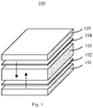
FIG. 1 is a diagram illustrating an electrochromic device. -
FIG. 2 is a diagram illustrating the change of transparency of an electrochromic device over time at different temperatures. -
FIG. 3 is a schematic diagram illustrating an electrochromic device in accordance with one or more embodiments of this specification. -
FIGS. 4A and 4B are cross-sectional views of an electrode layer with high conductive bars in an electrochromic device in accordance with one or more embodiments of this specification. -
FIGS. 5A and 5B are top plan views of electrochromic devices in accordance with one or more embodiments of this specification. -
FIG. 6 is a three-dimensional (3-D) diagram illustrating an electrode layer in an electrochromic device in accordance with one embodiment of this specification. -
FIG. 7 is a schematic diagram illustrating an electrochromic device in accordance with one or more embodiments of this specification. -
FIG. 8 is a flowchart illustrating a method of manufacturing an electrochromic device in accordance with one embodiment of this specification. -
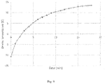
FIG. 9 is a diagram illustrating a change of device temperature over time for an electrochromic device in accordance with one or more embodiments of this specification. - Specific, non-limiting embodiments of the present invention will now be described with reference to the drawings. Particular features and aspects of any embodiment disclosed herein may be used and/or combined with particular features and aspects of any other embodiment disclosed herein. It should be understood that such embodiments are by way of example and are merely illustrative of a number of embodiments within the scope of the present invention. Various changes and modifications obvious to one skilled in the art to which the present invention pertains are deemed to be within the spirit, scope and contemplation of the present invention as further defined in the appended claims.
- While examples and features of disclosed principles are described herein, modifications, adaptations, and other implementations are possible without departing from the spirit and scope of the disclosed embodiments. Also, the words "comprising," "having," "containing," and "including," and other similar forms are intended to be equivalent in meaning and be open ended in that an item or items following any one of these words is not meant to be an exhaustive listing of such item or items, or meant to be limited to only the listed item or items. It must also be noted that as used herein and in the appended claims, the singular forms "a," "an," and "the" include plural references unless the context clearly dictates otherwise.
- The embodiments illustrated herein are described in sufficient detail to enable those skilled in the art to practice the teachings disclosed. Other embodiments may be used and derived therefrom, such that structural and logical substitutions and changes may be made without departing from the scope of this disclosure. The Detailed Description, therefore, is not to be taken in a limiting sense, and the scope of various embodiments is defined by the appended claims, along with the full range of equivalents to which such claims are entitled.
-
FIG. 1 is a diagram illustrating an electrochromic device. Referring toFIG. 1 , theelectrochromic device 100 may include anelectrolyte layer 103 that is sandwiched by anelectrochromic layer 102 and acharge storage layer 104. These three layers may be further sandwiched by two conductive substrates, i.e., a bottomconductive substrate 101 and a topconductive substrate 105, as shown inFIG. 1 . - The
electrochromic device 100 is a current-driving device. When a voltage is applied on the conductive substrates, the electrons, driven by the electric field established between the conductive substrates, may be injected into theelectrochromic layer 102 and change the redox state of the material, resulting in a change in the optical transmittance of theelectrochromic layer 102. Meanwhile, ions in theelectrolyte layer 103 may move towards thecharge storage layer 104 and theelectrochromic layer 102 to compensate the change of the redox state. The arrows inFIG. 1 indicate the current direction through the electrochromic device. - An electrolyte is necessary in electrochromic device to provide mobile ions to dope or de-dope the electrochromic material. The intrinsic switching speed of an electrochromic device is determined by the ion conductivities. With faster mobile ions, the ions could reach the electrochromic layer from the electrolyte layer in a shorter time. The speed of the ions depends on several factors, one of which is the temperature. It's widely known that low temperature freezes the movement of the ions, making it difficult to reach the electrochromic layer.
FIG. 2 is a diagram illustrating the change of transparency of an electrochromic device over time at different temperatures. As shown inFIG. 2 , a low temperature (e.g., -10 °C) not only causes the transparency of an electrochromic device to change slower compared to the counterpart operated at a room temperature, it also reduces the range of the transparency. - Smart glasses in buildings and vehicles frequently work in operating temperatures that are well below zero Celsius degree, and are expected to maintain the same switching speed as that in room temperature. Low operating temperature, however, may slow down the switching speed, and thus adversely affect the performance of the smart glasses. To overcome the slow movement of the ions at low temperature, this specification provides a self-heating electrochromic device that includes an internal heating mechanism, which may increase the temperature of the electrochromic device at a low temperature, thereby restoring the switching speed of the device.
-
FIG. 3 is a schematic diagram illustrating an electrochromic device in accordance with one or more embodiments of this specification.FIGS. 4A and 4B are cross-sectional views of an electrode layer with high conductive bars in the electrochromic device.FIGS. 5A and 5B are top plan views of the electrochromic devices in accordance with one or more embodiments of this specification. The electrochromic device will be described below in details with reference to these drawings. - As shown in
FIG. 3 , in one embodiment, theelectrochromic device 300 may include abottom electrode layer 301 and abottom substrate 330 attached to each other; atop substrate 340 and atop electrode layer 305 attached to each other; and anelectrochromic layer 302 disposed on an interior surface of thebottom electrode layer 301; acharge storage layer 304 disposed on an interior surface of thetop electrode layer 305; and anelectrolyte layer 303 disposed between theelectrochromic layer 302 and thecharge storage layer 304 and sandwiched by theelectrochromic layer 302 and thecharge storage layer 304. Thebottom electrode layer 301, theelectrochromic layer 302, theelectrolyte layer 303, thecharge storage layer 304, and thetop electrode layer 305 may be sandwiched by thebottom substrate 330 and thetop substrate 340. - The
electrochromic device 300 further includes two first highconductive bars 311/312 respectively provided on a surface of thebottom electrode layer 301 away from the bottom substrate 330 (note that, inFIG. 3 , one of the two first highconductive bars 311/312 is occluded, so only one is shown). Thebottom substrate 330 may be attached to the exterior surface of thebottom electrode layer 301, and thetop substrate 340 may be attached to the exterior surface of thetop electrode layer 305. - The two first high
conductive bars 311/312 may be provided along two edges of thebottom electrode layer 301, and configured to generate a current in thebottom electrode layer 301 in response to an external voltage (i.e., a first thermal voltage) applied on the first highconductive bars 311/312. The current in thebottom electrode layer 301 may heat theelectrochromic device 300. Thebottom electrode layer 301 and thetop electrode layer 305 may be configured to accept a voltage (i.e., a transition voltage) to cause a change on the optical transmittance of theelectrochromic device 300. - In this specification, "exterior surface" of an electrode layer refers to the surface of the electrode layer facing away from the interior of the electrochromic device 300 (e.g., the electrolyte layer 303), and "interior surface" of an electrode layer refers to a surface of the electrode layer facing towards the interior of the
electrochromic device 300. Therefore, as shown inFIG. 3 , since the surface of thebottom electrode layer 301 away from thebottom substrate 330 is the interior surface of thebottom electrode layer 301, the two first highconductive bars 311/312 are located on the interior surface of thebottom electrode layer 301. - The
bottom electrode layer 301 and thetop electrode layer 305 may each be transparent in at least part of the visible regions of the electromagnetic spectrum. They may have the same or different dimensions and comprise the same or different material. Thebottom electrode layer 301 and thetop electrode layer 305 may also each independently have a single layer or multilayer structure. Suitable material for thebottom electrode layer 301 and thetop electrode layer 305 may include, but is not limited to, tin doped indium oxide (ITO), fluorine doped indium oxide, antimony doped indium oxide, zinc doped indium oxide (IZO), aluminum doped zinc oxide, silver nanowires, carbon nanotube films, patterned metals on glass or plastic substrates, metal mesh, metal grid, dielectric metal dielectric (DMD), combinations thereof, and/or other such transparent material exhibiting sufficient electrical conductance. In preferred aspects, thebottom electrode layer 301 and thetop electrode layer 305 may comprise ITO. - The
electrochromic layer 302 may include one or more electrochromic materials. Suitable electrochromic materials for theelectrochromic layer 302 may include, but not limited to, inorganic material, conjugated polymers, small organic molecules, metal salts, combinations thereof, etc. In some embodiments, the electrochromic material of theelectrochromic layer 302 may include a metal oxide such as MoO3, V2O5, Nb2O5, WO3, TiO2, Ir(OH)x, SrTiO3, ZrO2, La2O3, CaTiO3, sodium titanate, potassium niobate, combinations thereof, etc. In some embodiments, the electrochromic material of theelectrochromic layer 302 may include a metal salt (e.g., FeCl3, etc.). In some embodiments, the electrochromic material of theelectrochromic layer 302 may include a conductive polymer such as poly-3,4-ethylenedioxy thiophene (PEDOT), poly-2,2'-bithiophene, polypyrrole, polyaniline (PANI), polythiopene, polyisothianaphthene, poly(o-aminophenol), polypyridine, polyindole, polycarbazole, polyquinone, octacyanophthalocyanine, combinations thereof, etc. Moreover, the electrochromic material of theelectrochromic layer 302 may include materials such as viologen, anthraquinone, phenocyazine, combinations thereof, etc. - The first high
conductive bars 311/312 may each be made of conductive materials. For example, the first highconductive bars 311/312 may be conductive paste such as silver paste, conductive tapes, or embedded metal wires formed along one or more edges of the corresponding electrode layers. - In some embodiments, as shown in
FIG. 3 , in additional to the first highconductive bars 311/312 respectively provided on two edges of thebottom electrode layer 301, theelectrochromic device 300 may further include two second highconductive bars 321/322 respectively provided on a surface of thetop electrode layer 305 away from thetop substrate 340. More specifically, the two second highconductive bars 321/322 may be provided along two edges of thetop electrode layer 305. The two second highconductive bars 321/322 may be configured to generate a current in thetop electrode layer 305 in response to an external voltage (e.g., a second thermal voltage) applied on the second highconductive bars 321/322. The current in thetop electrode layer 305 may heat theelectrochromic device 300. The second highconductive bars 321/322 may be made of the same material of the first highconductive bars 311/312. Since the surface of thetop electrode layer 305 away from thetop substrate 340 is the interior surface of thetop electrode layer 305, the two second highconductive bars 321/322 are located on the interior surface of thetop electrode layer 305. - The first thermal voltage may be the same as or different from the second thermal voltage, and this specification is not limited in this regard. For ease of the description, in some parts of this specification, the voltage applied on the first high
conductive bars 311/312 (i.e., the first thermal voltage) or that applied on the second highconductive bars 321/322 (i.e., the second thermal voltage) may be generally referred to as "the thermal voltage." However, it should be understood that, in some embodiments, these two voltages may be different. - In some embodiments, the
electrolyte layer 303 may be made of solid polymer electrolyte. That is, theelectrolyte layer 303 may be a solid polymer electrolyte layer. The solid polymer electrolyte layer may include a framework of one or more polar crystalline polymers, one or more polar amorphous polymers, and one or more electrolyte salts. In some embodiments, one or more of the one or more polar crystalline polymers or the one or more polar amorphous polymers are ionic conductive. In some embodiments, the solid polymer electrolyte may be formed by microphase separation of the components. - The one or more polar crystalline polymers may include one or more of: C, N, F, O, H, P, etc. In some embodiments, the one or more polar crystalline polymers may have an average molecular weight of about 10,000 Daltons or greater. Suitable polar crystalline polymers may include, but are not limited to, Nylon, Polyethylene terephthalate, Poly(methyl methacrylate) (PMMA), polyacrylamide, polyimide, polyvinylchloride (PVC), Polybutylene terephthalate (PBT), Polyether ether ketone (PEEK), Polytetrafluoroethylene (PTFE), Polyvinylidene fluoride (PVDF), Poly(vinylidene fluoride-co-hexafluoropropylene) (PVDF-HFP), high molecular weight polyethylene oxide, polyphenylene sulfide, polyetherimide, polyethersulfone, combinations thereof, etc. In embodiments where a plurality of polar crystalline polymers are present, the polar crystalline polymers may be crosslinked to form a network having enhanced mechanical properties. In some embodiments, the total amount of polar crystalline polymers may be in a range from about 0 wt.% to about 60 wt.% based on the total weight of the solid polymer electrolyte.
- The one or more polar amorphous polymers may include one or more of: C, N, O, F, H, P, Si, etc. In some embodiments, the one or more polar amorphous polymers have low crystallinity. The one or more polar amorphous polymers may have a glass transition temperature (Tg) of -20 °C or lower. Suitable polar amorphous polymers may include, but are not limited to, polyureathane, polysiloxane, polyethylene oxide, branched polymers, combinations thereof, etc. In some embodiments, one or more of the polar amorphous polymers may have a sufficient amorphicity so as to achieve sufficient ionic conductivity. In some embodiments, the total amount of polar amorphous polymers may be in a range from about 0 wt.% to about 70 wt.% based on the total weight of the solid polymer electrolyte.
- As noted above, the solid polymer electrolyte may include one or more electrolyte salts. In some embodiments, the one or more electrolyte salts may comprise one or more organic salts. In some embodiments, the one or more electrolyte salts may comprise one or more inorganic salts (e.g., metal salts). Suitable electrolyte salts may include, but are not limited to, LiTFSI, LiPF6, LiBF4, LiClO4, LiCF3SO3, LiN(CF3SO2)2, LiSbFg, LiAsF6, LiN(CF3CF2SO2)2, (C2H5)4NBF4, (C2H5)3CH3NBF4, LiI, combinations thereof, etc. In some embodiments, the total amount of electrolyte salt may be in a range from about 10 wt.% to about 50 wt.% based on the total weight of the solid polymer electrolyte.
- In some embodiments, the one or more polar amorphous polymers and the one or more electrolyte salts may be substantially miscible with the framework of the one or more polar crystalline polymers. Preferably, the components of the solid polymer electrolyte may be compatible with each other and can be blended (e.g., via solution processing or extrusion) into a transparent film without any observable particles.
- The solid polymer electrolyte is distinguishable from conventional liquid electrolytes, as well as gel polymer electrolytes including an ionic liquid therein. In other words, the presently disclosed solid polymer electrolyte may be an all solid polymer electrolyte, and does not include any liquid or gel components therein. The presently disclosed solid polymer electrolyte may also be transparent in some aspects. For example, the presently disclosed solid polymer electrolyte may have a transparency of 80% or higher. Additionally, the solid polymer electrolyte may have an ionic conductivity in a range from about 10-6 S/cm to about 10-3 S/cm.
- The
electrochromic device 300 may additionally include electrical power supplies (not shown) configured to supply the transition voltage between thebottom electrode layer 301 and thetop electrode layer 305, and the first thermal voltage between the first highconductive bars 311/312 and/or the second thermal voltage between the second highconductive bars 321/322. - In some embodiments, the two first high
conductive bars 311/312 may be parallel with each other. For theelectrochromic device 300 that includes two second highconductive bars 321/322, the second highconductive bars 321/322 may be parallel with each other. In some other examples, the two first highconductive bars 311/312 may not be parallel with each other, and the two second highconductive bars 321/322 may not be parallel with each other. This specification is not limited in this regard. - The two first high
conductive bars 311/312 may be provided respectively along two opposing edges of thebottom electrode layer 301, and the two second highconductive bars 321/322 may be provided respectively along two opposing edges of thetop electrode layer 305. -
FIG. 4A is a cross-sectional view of thebottom electrode layer 301 and the first highconductive bars 311/312. As shown inFIG. 4A , the two first highconductive bars 311/312 may be parallel with each other and respectively provided along the left and the right edges of thebottom electrode layer 301. -
FIG. 4B shows another cross-sectional view of the structure ofFIG. 4A . As shown inFIG. 4B , the two first highconductive bars 311/312 may be attached to the interior surface of thebottom electrode layer 301. By applying the first thermal voltage between the first highconductive bars 311/312, an electrical field may be generated in thebottom electrode layer 301 between the first highconductive bars 311/312. Thebottom electrode layer 301 has a finite conductivity, and thus is basically a resistor. Therefore thebottom electrode layer 301 may generate heat as a current flowing between the first highconductive bars 311/312. In this process, thebottom electrode layer 301 may work as a heat generating element for the electrochromic device. According to specific working conditions and requirements, a proper first thermal voltage may be chosen, so that thebottom electrode layer 301 may generate sufficient heat to keep the electrochromic device in a desired operating temperature. - If the
electrochromic device 300 includes two second highconductive bars 321/322. The two second highconductive bars 321/322 may be respectively provided along two opposing edges of thetop electrode layer 305. The second highconductive bars 321/322 may be provided on thetop electrode layer 305 in a similar manner as the first highconductive bars 311/312 being provided on thebottom electrode layer 301, thus relevant parts in the foregoing descriptions may be referred to for details, which are not repeatedly presented herein for the sake of conciseness. - It should be understood that
FIGS. 4A and 4B only show one possible arrangement of the high conductive bars on the electrode layer, and are not intended to be limiting. The number, specific shapes, and relative positions of the high conductive bars are not limited by this example. In some examples, more than two (e.g., four, six, or eight) high conductive bars may be provided along the edges of the electrode layer, and the high conductive bars may be provided on the top of, on the side to, or beneath the bottom of an electrode layer according to specific requirements. - In some embodiments, the
electrochromic device 300 may include both the first highconductive bars 311/312 and the second highconductive bars 321/322. To prevent short circuit between thebottom electrode layer 301 and thetop electrode layer 305 through the high conductive bars positioned along the edges of the electrode layers, the projections of the first highconductive bars 311/312 and the second highconductive bars 321/322 on a plane parallel with thebottom electrode layer 301 may be separated from each other. -
FIGS. 5A and 5B are top plan views of two exemplary electrochromic devices of this specification. In one example, as shown inFIG. 5A , two first highconductive bars 511/512 may be respectively provided along two opposing edges (i.e., left and right edges inFIG. 5A ) of the bottom electrode layer. Two second highconductive bars 521/522 may be respectively provided along two opposing edges (i.e., top and bottom edges inFIG. 5A ) of the top electrode layer. To avoid short circuit between the bottom electrode layer and the top electrode layer, the first highconductive bars 511/512 and the second highconductive bars 521/522 may be provided on different edges of the corresponding electrode layer in the top plan view. That is, the projections of the first highconductive bars 511/512 and the second highconductive bars 521/522 on the a plane parallel with the bottom electrode layer are separated from each other. More specifically, when viewed from a direction perpendicular to the interior surface of the bottom electrode layer, the first highconductive bars 511/512, and the second highconductive bars 521/522 are separated from each other, as shown inFIG. 5A . - In another example, as shown in
FIG. 5B , the two first highconductive bars 511/512 may be respectively provided on two adjacent edges (i.e., left and top edges inFIG. 5B ) of the bottom electrode layer, and form a "L" shape pattern. The two second highconductive bars 521/522 may be respectively provided on two adjacent edges (i.e., right and bottom edges inFIG. 5B ) of the top electrode layer, and form a "L" shape pattern. To avoid short circuit between the top electrode layer and the bottom electrode layer, the projections of the two first highconductive bars 511/512 and the two second highconductive bars 521/522 on a plane parallel with the bottom electrode layer may be separated from each other. More specifically, when viewed from a direction perpendicular to the top surface (i.e., the interior surface) of the bottom electrode layer, the first highconductive bars 511/512, and the second highconductive bars 521/522 may be separated from each other, as shown inFIG. 5B . - The thermal voltage may be determined based on factors such as the size of the electrode layer, the environmental temperature, and the resistance between the high conductive bars. To facilitate the description,
FIG. 6 shows an exemplary electrode layer that has a length of l, a width of w, and a thickness of t. Assuming that two first high conductive bars (not shown inFIG. 6 ) are respectively provided along the left and right edges of the electrode layer, when the thermal voltage is applied between the two high conductive bars, the current I may flow from left to right, as shown inFIG. 6 . The resistance R of the electrode layer may be determined by:
- where ρ is the resistivity, and Rs is the sheet resistance. The heat power P generated by the electrode layer may be determined by:

where V is the thermal voltage. - In some embodiments, the resistance between the two first high conductive bars may be in a range of 1-100 Ω, the resistance between the two second high conductive bars may be in a range of 1-100 Ω, and the thermal voltage may be in a range of 1-100 V. Apparently, these settings are just one setting that can be used for the electrochromic device of this specification and are not intended to be limiting. These values may be adjusted according to specific needs.
- In the aforementioned embodiments, each of the top electrode layer and the bottom electrode layer is responsible for inducing optical change and generating heat. That is, on one hand, a transition voltage may be applied between the top and the bottom electrode layers to generate an electrical field therebetween to drive the electrons/ions movement, resulting in a change of the optical characteristics of the electrochromic device. On the other hand, each of the top electrode layer and the bottom electrode layer may work as a heat generating element. When a thermal voltage is applied on the high conductive bars provided along the edges of an electrode layer, a current may be generated within the electrode layer, and the electrode layer may work as a heating element to heat the electrochromic device. When the environmental temperature is lower than an optimal operating temperature, the heat generated by the electrode layer may increase the operating temperature, thereby improving the switching speed and the performance of the electrochromic device.
- This specification further provides another electrochromic device. This electrochromic device has similar structure and composition with the electrochromic devices in the foregoing embodiments except that, instead of using one type of electrode layer, two types of electrode layers are provided in this electrochromic device, one dedicated for optical change inducing purpose, and the other dedicated for heat generating purpose.
- More specifically, the electrochromic device may include: a bottom heater electrode layer and a bottom optical electrode layer respectively attached to an exterior surface and an interior surface of a bottom substrate; a top heater electrode layer and a top optical electrode layer respectively attached to an exterior surface and an interior surface of a top substrate; an electrochromic layer disposed on an interior surface of the bottom optical electrode layer; a charge storage layer disposed on an interior surface of the top optical electrode layer; an electrolyte layer disposed between the electrochromic layer and the charge storage layer and sandwiched by the electrochromic layer and the charge storage layer. The bottom optical electrode layer, the electrochromic layer, the electrolyte layer, the charge storage layer, and the top optical electrode layer may be sandwiched by the bottom substrate and the top substrate. The bottom optical electrode layer and the top optical electrode layer may be configured to accept a transition voltage to cause a change on an optical transmittance of the electrochromic device.
- The electrochromic device may further include two first high conductive bars located on a surface of the bottom heater electrode layer away from the bottom substrate. The two first high conductive bars may be configured to, in response to a first thermal voltage applied on the first high conductive bars, generate a current in the bottom heater electrode layer to change a temperature of the electrochromic device.
- In some embodiments, the electrochromic device may further include two second high conductive bars located on a surface of the top heater electrode layer away from the top substrate. The two second high conductive bars may be configured to, in response to a second thermal voltage applied on the second high conductive bars, generate a current in the top heater electrode layer to change the temperature of the electrochromic device.
- The two first high conductive bars may be respectively provided along two edges of the bottom heater electrode layer on a surface of the bottom heater electrode layer away from the bottom substrate. The two second high conductive bars may be respectively provided along two edges of the top heater electrode layer on a surface of the top heater electrode layer away from the top substrate.
- Relevant parts in the description of the electrochromic devices in the foregoing embodiments may be referred to for detailed structure and composition of various layers of the electrochromic device, which are not repeatedly described herein for the sake of conciseness.
-
FIG. 7 is a schematic diagram illustrating an electrochromic device in accordance with one or more embodiments of this specification. As shown inFIG. 7 , theelectrochromic device 700 may include a bottomoptical electrode layer 701; anelectrochromic layer 702 on the bottomoptical electrode layer 701; anelectrolyte layer 703 on theelectrochromic layer 702; acharge storage layer 704 on theelectrolyte layer 703; and a topoptical electrode layer 705 on thecharge storage layer 704. A transition voltage may be applied between the topoptical electrode layer 705 and the bottomoptical electrode layer 701 to generate an electric field for inducing a change of the optical characteristics. Relevant parts in the foregoing embodiments may be referred to for details of this electrochromic device, which will not be repeatedly presented herein for the sake of conciseness. - In some embodiments, the
electrochromic device 700 may further include a pair of transparent substrate (i.e., abottom substrate 730 and a top substrate 740). The bottomoptical electrode layer 701, theelectrochromic layer 702, theelectrolyte layer 703, thecharge storage layer 704, and the topoptical electrode layer 705 may be sandwiched by thebottom substrate 730 and thetop substrate 740. Thebottom substrate 730 and thetop substrate 740 may be rigid substrates or flexible substrates, may have the same or different dimensions, and may comprise the same or different material, etc. Suitable material for thebottom substrate 730 and/or thetop substrate 740 may include, but not limited to, glass, polymeric materials, Polyethylene terephthalate (PET), plastic materials, and/or other materials which are transparent in at least part of the visible region of the electromagnetic spectrum. In some embodiments, thebottom substrate 730 and thetop substrate 740 may comprise glass. - In some embodiments, the
electrochromic device 700 may further include one or more heater electrode layers dedicated for heat generation purpose. As shown inFIG. 7 , a bottomheater electrode layer 706 may be provided on a side of thebottom substrate 730 opposing the bottomoptical electrode layer 701. That is, the bottomheater electrode layer 706 and the bottomoptical electrode layer 701 may be respectively provided on two opposing surfaces of thebottom substrate 730. Two first highconductive bars 711/712 may be respectively provided along two opposing edges of the bottomheater electrode layer 706 on a surface of the bottomheater electrode layer 706 away from thebottom substrate 730. A first thermal voltage may be applied between the two first highconductive bars heater electrode layer 706, and the bottomheater electrode layer 706 may work as a heat generating element to heat theelectrochromic device 700. Thebottom heater electrode 706 and the bottomoptical electrode layer 701 may be made of a same material or different materials, and this specification is not limited in this regard. - The
electrochromic device 700 shown inFIG. 7 is similar to theelectrochromic device 300 shown inFIG. 3 . The difference between these two electrochromic devices is that, in theelectrochromic device 700, the first highconductive bars 711/712 are respectively provided along two opposing edges of a dedicated electrode layer (i.e., the bottom heater electrode layer 706) for heat generation purpose. While in theelectrochromic device 300, the high conductive bars are respectively provided along two opposing edges of the bottom electrode layer which also connects to a transition voltage and serves for inducing optical change purpose. - It should be understood that
FIG. 7 only shows one heater electrode layer (i.e., the bottom heater electrode layer 706) and is not intended to be limiting. In some embodiments, the electrochromic device may further include a top heater electrode layer (not shown inFIG. 7 ) on an exterior surface thetop substrate 740. That is, the top heater electrode layer and the topoptical electrode layer 705 may be respectively provided on two opposing surfaces of thetop substrate 740. Two second high conductive bars (not shown inFIG. 7 ) may be respectively provided along two edges of the top heater electrode layer, and configured to, in response to a second thermal voltage applied on the second high conductive bars, generate a current in the top heater electrode layer to heat theelectrochromic device 700. The two second high conductive bars may be attached to a surface of the top heater electrode layer away from the top substrate. - In some embodiments, the electrochromic device may include only the bottom heater electrode layer (and the associated high conductive bars), only the top heater electrode layer (and the associated high conductive bars), or both, and this specification is not limited in this regard.
- In the electrochromic device disclosed in this specification, two high conductive bars may be respectively provided along two edges of the top electrode layer and/or bottom electrode layer. When a thermal voltage is applied on the two high conductive bars, the electrode layer(s) may work as heat generating element(s) to heat the electrochromic device. When the environmental temperature is lower than an optimal operating temperature, the heat generated by the electrode layer(s) may increase the operating temperature, thereby improving the switching speed and the performance of the electrochromic device.
- Based on the aforementioned electrochromic devices, this specification further provides an electrochromic device manufacturing methods.
FIG. 8 is a flowchart illustrating a method of manufacturing an electrochromic device in accordance with one embodiment of this specification. This method will be described below in details with reference toFIG. 8 . - Referring to
FIG. 8 , the manufacturing method may include the following steps S810 through S840. - In step S810, a bottom substrate and a bottom electrode layer may be formed. The bottom substrate may be attached to the bottom electrode layer.
- In step S820, two first high conductive bar may be formed on a surface of the bottom electrode layer away from the bottom substrate. The two first high conductive bars may be configured to generate a current in the bottom electrode layer in response to a first thermal voltage applied on the first high conductive bars to heat the electrochromic device. More specifically, the two first high conductive bars may respectively be formed along two edges of the bottom electrode layer.
- In step S830, a top substrate and a top electrode layer may be formed. The top substrate may be attached to the top electrode layer.
- In step S840, an electrochromic, an electrolyte layer, and a charge storage layer that are sandwiched by the top electrode layer and the bottom electrode layer may be formed.
- More specifically, step S840 may include the following sub-steps: forming an electrochromic layer on an interior surface of the bottom electrode layer; forming a charge storage layer on an interior surface of the top electrode layer; and forming an electrolyte layer disposed between the electrochromic layer and the charge storage layer and sandwiched by the electrochromic layer and the charge storage layer. The bottom electrode layer, the electrochromic layer, the electrolyte layer, the charge storage layer, and the top electrode layer may be sandwiched by the top substrate and the bottom substrate.
- A transition voltage may be applied between the bottom electrode layer and the top electrode layer, and the optical transmittance of the electrochromic device may change in response to the transition voltage.
- In some embodiments, the aforementioned method may further include steps to form two second high conductive bars on the top electrode layer. That is, the aforementioned method may further include: forming two second high conductive bars on a surface of the top electrode layer away from the top substrate. The second high conductive bars may be configured to generate a current in the top electrode layer in response to a second thermal voltage applied on the second high conductive bars to heat the electrochromic device. More specifically, the two second high conductive bars may be respectively formed along two edges of the top electrode layer.
- In some embodiments, the first high conductive bars and the second high conductive bars may each made of a conductive paste, a conductive tape, or an embedded metal wire.
- In some embodiments, the first high conductive bars may be formed along edges of the bottom electrode layer, respectively, and the second high conductive bars may be formed along edges of the top electrode layer, respectively.
- In some embodiments, projections of the first high conductive bars and the second high conductive bars on a plane parallel with the bottom electrode layer may be separated from each other.
- In some embodiments, the forming two first high conductive bars on a surface of the bottom electrode layer away from the bottom substrate may include: forming the two first high conductive bars parallel with each other and respectively along two opposing edges of the bottom electrode layer. The forming two second high conductive bars on a surface of the top electrode layer away from the top substrate may include: forming the two second high conductive bars parallel with each other and respectively along two opposing edges of the top electrode layer.
- In another example, the forming two first high conductive bars on a surface of the bottom electrode layer away from the bottom substrate may include: forming the two first high conductive bars respectively along two adjacent edges of the bottom electrode layer. The forming two second high conductive bars on a surface of the top electrode layer away from the top substrate may include: forming the two second high conductive bars respectively along two adjacent edges of the top electrode layer.
- In some embodiments, the top electrode layer and the bottom electrode layer may each have a square shape. The top electrode layer and the bottom electrode layer may have the same size or different sizes. This specification is not limited in this regard.
- In some embodiments, a resistance between the two first high conductive bars may be in a range of 1-100 Ω, a resistance between the two second high conductive bars may be in a range of 1-100 Ω, and the first thermal voltage and the second thermal voltage may each be in a range of 1-100 V.
- In some embodiments, the bottom electrode layer may include a bottom heater electrode layer and a bottom optical electrode layer. The forming a bottom substrate and a bottom electrode layer attached to each other may include: forming the bottom heater electrode layer and the bottom optical electrode layer respectively attached to two opposing surfaces of the bottom substrate. In one example, the bottom heater electrode layer may be attached to an exterior surface of the bottom substrate, and the bottom optical electrode layer may be attached to an interior surface of the bottom substrate. The forming two first high conductive bars on a surface of the bottom electrode layer away from the bottom substrate may include: forming the two first high conductive bars respectively along two edges of the bottom heater electrode layer on a surface of the bottom heater electrode layer away from the bottom substrate.
- The top electrode layer may include a top optical electrode layer and a top heater electrode layer. The forming a top substrate and a top electrode layer attached to each other may include: forming a top heater electrode layer and a top optical electrode layer respectively attached to two opposing surfaces of the top substrate. In one example, the top heater electrode layer may be attached to an exterior surface of the top substrate, and the top optical electrode layer may be attached to an interior surface of the top substrate. The forming two second high conductive bars on a surface of the top electrode layer away from the top substrate may include: forming the two second high conductive bars respectively along two edges of the top heater electrode layer on a surface of the top heater electrode layer away from the top substrate. The transition voltage may be applied between the bottom optical electrode layer and the top electrode layer.
- In some embodiments, the electrolyte layer may be a solid polymer electrolyte layer including one or more polar crystalline polymers and one or more polar amorphous polymers. A total amount of polar crystalline polymers may be in a range of 0 wt. % to 60 wt. % of a total weight of the solid polymer electrolyte layer. A total amount of polar amorphous polymers may be in a range of 0 wt. % to 70 wt. % of the total weight of the solid polymer electrolyte layer.
- Relevant parts in the foregoing embodiments may be referred to for details of the electrochromic devices, which will not be repeatedly presented herein for the sake of conciseness.
- It should be understood that the order these steps are presented in the above description is just one of various possible implementations, and is not intended to be limiting. Some or all of these steps may be performed simultaneously, and one or more steps may be performed in an order that is earlier than or later than the order specified in the above description. This specification is not limited in this regard.
- In the manufacturing methods herein disclosed, two high conductive bars may be formed along two edges of the top electrode layer and/or the bottom electrode layer. When a thermal voltage is applied on the high conductive bars, the electrode layer(s) may work as heat generating element(s) to heat the electrochromic device. When the environmental temperature is lower than an optimal operating temperature, the heat generated by the electrode layer(s) may increase the operating temperature, thereby improving the switching speed and the performance of the electrochromic device.
-
FIG. 9 is a diagram illustrating a change of device temperature over time for an electrochromic device in accordance with one or more embodiments of this specification. In the example ofFIG. 9 , an electrochromic device is placed at an environmental temperature of -10°C. The resistance R of the electrode layer is around 8 Ω. When a thermal voltage of 15 V is applied on the high conductive bars on the electrode layer, the current on the electrode layer is measured at 1.88 A. As shown inFIG. 9 , the device temperature is increased to above zero degree in a few minutes, indicating that the electrochromic device can effectively increase the operating temperature. - While examples and features of disclosed principles are described herein, modifications, adaptations, and other implementations are possible without departing from the spirit and scope of the disclosed embodiments. Also, the words "comprising," "having," "containing," and "including," and other similar forms are intended to be equivalent in meaning and be open ended in that an item or items following any one of these words is not meant to be an exhaustive listing of such item or items, or meant to be limited to only the listed item or items. It must also be noted that as used herein and in the appended claims, the singular forms "a," "an," and "the" include plural references unless the context clearly dictates otherwise.
- The embodiments illustrated herein are described in sufficient detail to enable those skilled in the art to practice the teachings disclosed. Other embodiments may be used and derived therefrom, such that structural and logical substitutions and changes may be made without departing from the scope of this disclosure. The Detailed Description, therefore, is not to be taken in a limiting sense, and the scope of various embodiments is defined by the appended claims, along with the full range of equivalents to which such claims are entitled.
-
- 1. An electrochromic device, comprising:
- a bottom substrate and a bottom electrode layer attached to each other;
- a top substrate and a top electrode layer attached to each other;
- an electrochromic layer disposed on an interior surface of the bottom electrode layer;
- a charge storage layer disposed on an interior surface of the top electrode layer;
- an electrolyte layer disposed between the electrochromic layer and the charge storage layer and sandwiched by the electrochromic layer and the charge storage layer, wherein the bottom electrode layer, the electrochromic layer, the electrolyte layer, the charge storage layer, and the top electrode layer are sandwiched by the bottom substrate and the top substrate, the bottom electrode layer and the top electrode layer are configured to accept a transition voltage to cause a change on an optical transmittance of the electrochromic device; and
- two first high conductive bars located on a surface of the bottom electrode layer away from the bottom substrate, wherein the two first high conductive bars are configured to, in response to a first thermal voltage applied on the first high conductive bars, generate a current in the bottom electrode layer to change a temperature of the electrochromic device.
- 2. The electrochromic device of
clause 1, further comprising:
two second high conductive bars located on a surface of the top electrode layer away from the top substrate, wherein the two second high conductive bars are configured to, in response to a second thermal voltage applied on the second high conductive bars, generate a current in the top electrode layer to change the temperature of the electrochromic device. - 3. The electrochromic device of clause 2, wherein the first high conductive bars and the second high conductive bars are each made of a conductive paste, a conductive tape, or an embedded metal wire.
- 4. The electrochromic device of clause 2, wherein the first high conductive bars are located along edges of the bottom electrode layer, respectively, and the second high conductive bars are located along edges of the top electrode layer, respectively.
- 5. The electrochromic device of clause 2, wherein projections of the first high conductive bars and the second high conductive bars on a plane parallel with the bottom electrode layer are separated from each other.
- 6. The electrochromic device of clause 5, wherein the two first high conductive bars are parallel with each other and respectively located along two opposing edges of the bottom electrode layer, and the two second high conductive bars are parallel with each other and respectively located along two opposing edges of the top electrode layer.
- 7. The electrochromic device of clause 5, wherein the two first high conductive bars are respectively located along two adjacent edges of the bottom electrode layer, and the two second high conductive bars are respectively located along two adjacent edges of the top electrode layer.
- 8. The electrochromic device of
clause 1, wherein the electrolyte layer is a solid polymer electrolyte layer including one or more polar crystalline polymers and one or more polar amorphous polymers, and wherein a total amount of polar crystalline polymers is in a range of 0 wt. % to 60 wt. % of a total weight of the solid polymer electrolyte layer, and a total amount of polar amorphous polymers is in a range of 0 wt. % to 70 wt. % of the total weight of the solid polymer electrolyte layer. - 9. An electrochromic device, comprising:
- a bottom heater electrode layer and a bottom optical electrode layer respectively attached to an exterior surface and an interior surface of a bottom substrate;
- a top heater electrode layer and a top optical electrode layer respectively attached to an exterior surface and an interior surface of a top substrate;
- an electrochromic layer disposed on an interior surface of the bottom optical electrode layer;
- a charge storage layer disposed on an interior surface of the top optical electrode layer;
- an electrolyte layer disposed between the electrochromic layer and the charge storage layer and sandwiched by the electrochromic layer and the charge storage layer, wherein the bottom optical electrode layer, the electrochromic layer, the electrolyte layer, the charge storage layer, and the top optical electrode layer are sandwiched by the bottom substrate and the top substrate, the bottom optical electrode layer and the top optical electrode layer are configured to accept a transition voltage to cause a change on an optical transmittance of the electrochromic device; and
- two first high conductive bars located on a surface of the bottom heater electrode layer away from the bottom substrate, wherein the two first high conductive bars are configured to, in response to a first thermal voltage applied on the first high conductive bars, generate a current in the bottom heater electrode layer to change a temperature of the electrochromic device.
- 10. The electrochromic device of clause 9, further comprising:
two second high conductive bars located on a surface of the top heater electrode layer away from the top substrate, wherein the two second high conductive bars are configured to, in response to a second thermal voltage applied on the second high conductive bars, generate a current in the top heater electrode layer to change the temperature of the electrochromic device. - 11. The electrochromic device of
clause 10, wherein the first high conductive bars and the second high conductive bars are each made of a conductive paste, a conductive tape, or an embedded metal wire. - 12. The electrochromic device of
clause 10, the first high conductive bars are located along edges of the bottom heater electrode layer, respectively, and the second high conductive bars are located along edges of the top heater electrode layer, respectively. - 13. The electrochromic device of clause 9, wherein the electrolyte layer is a solid polymer electrolyte layer including one or more polar crystalline polymers and one or more polar amorphous polymers, and wherein a total amount of polar crystalline polymers is in a range of 0 wt. % to 60 wt. % of a total weight of the solid polymer electrolyte layer, and a total amount of polar amorphous polymers is in a range of 0 wt. % to 70 wt. % of the total weight of the solid polymer electrolyte layer.
- 14. An electrochromic device manufacturing method, comprising:
- forming a bottom substrate and a bottom electrode layer attached to each other;
- forming two first high conductive bars on a surface of the bottom electrode layer away from the bottom substrate;
- forming a top substrate and a top electrode layer attached to each other; and
- forming an electrochromic layer, an electrolyte layer, and a charge storage layer sandwiched by the bottom electrode layer and the top electrode layer, wherein the electrolyte layer is sandwiched by the electrochromic layer and the charge storage layer, the bottom electrode layer, the electrochromic layer, the electrolyte layer, the charge storage layer, and the top electrode layer are sandwiched by the bottom substrate and the top substrate,
- wherein the two first high conductive bars are configured to, in response to a first thermal voltage applied on the first high conductive bars, generate a current in the bottom electrode layer to change a temperature of the electrochromic device, the bottom electrode layer and the top electrode layer are configured to accept a transition voltage to cause a change on an optical transmittance of the electrochromic device.
- 15. The method of clause 14, further comprising:
forming two second high conductive bars on a surface of the top electrode layer away from the top substrate, wherein the two second high conductive bars are configured to, in response to a second thermal voltage applied on the second high conductive bars, generate a current in the top electrode layer to change the temperature of the electrochromic device. - 16. The method of
clause 15, wherein the first high conductive bars and the second high conductive bars are each made of a conductive paste, a conductive tape, or an embedded metal wire. - 17. The method of
clause 15, wherein the first high conductive bars are formed along edges of the bottom electrode layer, respectively, and the second high conductive bars are formed along edges of the top electrode layer, respectively. - 18. The method of
clause 15, wherein projections of the first high conductive bars and the second high conductive bars on a plane parallel with the bottom electrode layer are separated from each other. - 19. The method of clause 18, wherein the forming two first high conductive bars on a surface of the bottom electrode layer away from the bottom substrate comprises:
- forming the two first high conductive bars parallel with each other and respectively along two opposing edges of the bottom electrode layer,
- and wherein the forming two second high conductive bars on a surface of the top electrode layer away from the top substrate comprises:
forming the two second high conductive bars parallel with each other and respectively along two opposing edges of the top electrode layer.
- 20. The method of clause 18, wherein the forming two first high conductive bars on a surface of the bottom electrode layer away from the bottom substrate comprises:
- forming the two first high conductive bars respectively along two adjacent edges of the bottom electrode layer,
- and wherein the forming two second high conductive bars on a surface of the top electrode layer away from the top substrate comprises:
forming the two second high conductive bars respectively along two adjacent edges of the top electrode layer.
Claims (15)
- An electrochromic device, comprising:a bottom substrate and a bottom electrode layer attached to each other;a top substrate and a top electrode layer attached to each other;an electrochromic layer disposed on an interior surface of the bottom electrode layer;a charge storage layer disposed on an interior surface of the top electrode layer;an electrolyte layer disposed between the electrochromic layer and the charge storage layer and sandwiched by the electrochromic layer and the charge storage layer, wherein the bottom electrode layer, the electrochromic layer, the electrolyte layer, the charge storage layer, and the top electrode layer are sandwiched by the bottom substrate and the top substrate, the bottom electrode layer and the top electrode layer are configured to accept a transition voltage to cause a change on an optical transmittance of the electrochromic device; andtwo first high conductive bars located on a surface of the bottom electrode layer away from the bottom substrate, wherein the two first high conductive bars are configured to, in response to a first thermal voltage applied on the first high conductive bars, generate a current in the bottom electrode layer to change a temperature of the electrochromic device.
- The electrochromic device of claim 1, further comprising:
two second high conductive bars located on a surface of the top electrode layer away from the top substrate, wherein the two second high conductive bars are configured to, in response to a second thermal voltage applied on the second high conductive bars, generate a current in the top electrode layer to change the temperature of the electrochromic device. - The electrochromic device of claim 2, wherein the first high conductive bars and the second high conductive bars are each made of a conductive paste, a conductive tape, or an embedded metal wire; and/orwherein the first high conductive bars are located along edges of the bottom electrode layer, respectively, and the second high conductive bars are located along edges of the top electrode layer, respectively; orwherein projections of the first high conductive bars and the second high conductive bars on a plane parallel with the bottom electrode layer are separated from each other.
- The electrochromic device of claim 3, wherein the two first high conductive bars are parallel with each other and respectively located along two opposing edges of the bottom electrode layer, and the two second high conductive bars are parallel with each other and respectively located along two opposing edges of the top electrode layer; or
wherein the two first high conductive bars are respectively located along two adjacent edges of the bottom electrode layer, and the two second high conductive bars are respectively located along two adjacent edges of the top electrode layer. - The electrochromic device of claim 1, wherein the electrolyte layer is a solid polymer electrolyte layer including one or more polar crystalline polymers and one or more polar amorphous polymers, and wherein a total amount of polar crystalline polymers is in a range of 0 wt. % to 60 wt. % of a total weight of the solid polymer electrolyte layer, and a total amount of polar amorphous polymers is in a range of 0 wt. % to 70 wt. % of the total weight of the solid polymer electrolyte layer.
- An electrochromic device, comprising:a bottom heater electrode layer and a bottom optical electrode layer respectively attached to an exterior surface and an interior surface of a bottom substrate;a top heater electrode layer and a top optical electrode layer respectively attached to an exterior surface and an interior surface of a top substrate;an electrochromic layer disposed on an interior surface of the bottom optical electrode layer;a charge storage layer disposed on an interior surface of the top optical electrode layer;an electrolyte layer disposed between the electrochromic layer and the charge storage layer and sandwiched by the electrochromic layer and the charge storage layer, wherein the bottom optical electrode layer, the electrochromic layer, the electrolyte layer, the charge storage layer, and the top optical electrode layer are sandwiched by the bottom substrate and the top substrate, the bottom optical electrode layer and the top optical electrode layer are configured to accept a transition voltage to cause a change on an optical transmittance of the electrochromic device; andtwo first high conductive bars located on a surface of the bottom heater electrode layer away from the bottom substrate, wherein the two first high conductive bars are configured to, in response to a first thermal voltage applied on the first high conductive bars, generate a current in the bottom heater electrode layer to change a temperature of the electrochromic device.
- The electrochromic device of claim 6, further comprising:
two second high conductive bars located on a surface of the top heater electrode layer away from the top substrate, wherein the two second high conductive bars are configured to, in response to a second thermal voltage applied on the second high conductive bars, generate a current in the top heater electrode layer to change the temperature of the electrochromic device. - The electrochromic device of claim 7, wherein the first high conductive bars and the second high conductive bars are each made of a conductive paste, a conductive tape, or an embedded metal wire; and/or
wherein the first high conductive bars are located along edges of the bottom heater electrode layer, respectively, and the second high conductive bars are located along edges of the top heater electrode layer, respectively. - The electrochromic device of claim 6, wherein the electrolyte layer is a solid polymer electrolyte layer including one or more polar crystalline polymers and one or more polar amorphous polymers, and wherein a total amount of polar crystalline polymers is in a range of 0 wt. % to 60 wt. % of a total weight of the solid polymer electrolyte layer, and a total amount of polar amorphous polymers is in a range of 0 wt. % to 70 wt. % of the total weight of the solid polymer electrolyte layer.
- An electrochromic device manufacturing method, comprising:forming a bottom substrate and a bottom electrode layer attached to each other;forming two first high conductive bars on a surface of the bottom electrode layer away from the bottom substrate;forming a top substrate and a top electrode layer attached to each other; andforming an electrochromic layer, an electrolyte layer, and a charge storage layer sandwiched by the bottom electrode layer and the top electrode layer, wherein the electrolyte layer is sandwiched by the electrochromic layer and the charge storage layer, the bottom electrode layer, the electrochromic layer, the electrolyte layer, the charge storage layer, and the top electrode layer are sandwiched by the bottom substrate and the top substrate,wherein the two first high conductive bars are configured to, in response to a first thermal voltage applied on the first high conductive bars, generate a current in the bottom electrode layer to change a temperature of the electrochromic device, the bottom electrode layer and the top electrode layer are configured to accept a transition voltage to cause a change on an optical transmittance of the electrochromic device.
- The method of claim 10, further comprising:
forming two second high conductive bars on a surface of the top electrode layer away from the top substrate, wherein the two second high conductive bars are configured to, in response to a second thermal voltage applied on the second high conductive bars, generate a current in the top electrode layer to change the temperature of the electrochromic device. - The method of claim 11, wherein the first high conductive bars and the second high conductive bars are each made of a conductive paste, a conductive tape, or an embedded metal wire.
- The method of claim 11, wherein the first high conductive bars are formed along edges of the bottom electrode layer, respectively, and the second high conductive bars are formed along edges of the top electrode layer, respectively; or
wherein projections of the first high conductive bars and the second high conductive bars on a plane parallel with the bottom electrode layer are separated from each other. - The method of claim 13, wherein the forming two first high conductive bars on a surface of the bottom electrode layer away from the bottom substrate comprises:forming the two first high conductive bars parallel with each other and respectively along two opposing edges of the bottom electrode layer,and wherein the forming two second high conductive bars on a surface of the top electrode layer away from the top substrate comprises:
forming the two second high conductive bars parallel with each other and respectively along two opposing edges of the top electrode layer. - The method of claim 13, wherein the forming two first high conductive bars on a surface of the bottom electrode layer away from the bottom substrate comprises:forming the two first high conductive bars respectively along two adjacent edges of the bottom electrode layer,and wherein the forming two second high conductive bars on a surface of the top electrode layer away from the top substrate comprises:
forming the two second high conductive bars respectively along two adjacent edges of the top electrode layer.
Applications Claiming Priority (1)
| Application Number | Priority Date | Filing Date | Title |
|---|---|---|---|
| US16/918,419 US11493817B2 (en) | 2020-07-01 | 2020-07-01 | Self-heating electrochromic device and manufacture thereof |
Publications (1)
| Publication Number | Publication Date |
|---|---|
| EP3933497A1 true EP3933497A1 (en) | 2022-01-05 |
Family
ID=76730469
Family Applications (1)
| Application Number | Title | Priority Date | Filing Date |
|---|---|---|---|
| EP21182953.6A Pending EP3933497A1 (en) | 2020-07-01 | 2021-06-30 | Self-heating electrochromic device and manufacture thereof |
Country Status (4)
| Country | Link |
|---|---|
| US (1) | US11493817B2 (en) |
| EP (1) | EP3933497A1 (en) |
| JP (1) | JP2022013899A (en) |
| CN (1) | CN113885266A (en) |
Citations (3)
| Publication number | Priority date | Publication date | Assignee | Title |
|---|---|---|---|---|
| US20030227663A1 (en) * | 2000-05-04 | 2003-12-11 | Anoop Agrawal | Chromogenic glazing |
| JP2015060109A (en) * | 2013-09-19 | 2015-03-30 | 凸版印刷株式会社 | Electrochromic display element |
| US20180100056A1 (en) * | 2016-10-11 | 2018-04-12 | Furcifer Inc. | Polymer electrolyte and electrochromic devices including polymer electrolyte |
Family Cites Families (12)
| Publication number | Priority date | Publication date | Assignee | Title |
|---|---|---|---|---|
| JPS61245143A (en) | 1985-04-23 | 1986-10-31 | Asahi Glass Co Ltd | Dimmer |
| JPH0295322U (en) | 1989-01-14 | 1990-07-30 | ||
| FR2649691B1 (en) * | 1989-07-11 | 1992-10-30 | Saint Gobain Vitrage Int | ELECTROCHROME GLAZING |
| FR2681444B1 (en) | 1991-09-16 | 1994-09-30 | Corning Inc | ELECTROCHROME DEVICE. |
| JPH08248451A (en) * | 1995-03-08 | 1996-09-27 | Canon Inc | Electrochromic element |
| GB9603851D0 (en) | 1996-02-23 | 1996-04-24 | Pilkington Plc | Electrochromic devices |
| US6906842B2 (en) * | 2000-05-24 | 2005-06-14 | Schott North America, Inc. | Electrochromic devices |
| US10429712B2 (en) | 2012-04-20 | 2019-10-01 | View, Inc. | Angled bus bar |
| US10761393B2 (en) | 2013-02-04 | 2020-09-01 | E-Vision, Llc | Electro-chromic devices including solid or quasi-solid electrolyte layers and methods of making the same |
| WO2016126460A2 (en) * | 2015-02-06 | 2016-08-11 | Proteq Technologies Llc | Electrochromic devices |
| KR102056095B1 (en) * | 2016-09-28 | 2019-12-16 | 주식회사 엘지화학 | Electrochromic device |
| KR102305919B1 (en) * | 2019-06-26 | 2021-09-29 | 한국기계연구원 | Active type electro-chromic device and active type electro-chromic window using the same |
-
2020
- 2020-07-01 US US16/918,419 patent/US11493817B2/en active Active
-
2021
- 2021-06-30 EP EP21182953.6A patent/EP3933497A1/en active Pending
- 2021-07-01 JP JP2021109854A patent/JP2022013899A/en active Pending
- 2021-07-01 CN CN202110742363.2A patent/CN113885266A/en active Pending
Patent Citations (3)
| Publication number | Priority date | Publication date | Assignee | Title |
|---|---|---|---|---|
| US20030227663A1 (en) * | 2000-05-04 | 2003-12-11 | Anoop Agrawal | Chromogenic glazing |
| JP2015060109A (en) * | 2013-09-19 | 2015-03-30 | 凸版印刷株式会社 | Electrochromic display element |
| US20180100056A1 (en) * | 2016-10-11 | 2018-04-12 | Furcifer Inc. | Polymer electrolyte and electrochromic devices including polymer electrolyte |
Also Published As
| Publication number | Publication date |
|---|---|
| US20220004072A1 (en) | 2022-01-06 |
| CN113885266A (en) | 2022-01-04 |
| US11493817B2 (en) | 2022-11-08 |
| JP2022013899A (en) | 2022-01-18 |
Similar Documents
| Publication | Publication Date | Title |
|---|---|---|
| JP5870182B2 (en) | Electrochromic devices | |
| US8094361B2 (en) | Polymer shutter compositions and devices for infrared systems | |
| CN108463912B (en) | Polymer electrolyte and electrochromic device including the same | |
| JP2016105150A (en) | Electrochromic device and manufacturing method of the same | |
| US20220342268A1 (en) | Electrochromic device having low-resistance transparent electrode structure | |
| KR102141635B1 (en) | Electrochromic device | |
| Wen et al. | Flexible batteries ahead | |
| EP4030228A1 (en) | Method of manufacturing flexible electrochromic device | |
| KR20170126210A (en) | Electrochromic device | |
| CN111399300B (en) | Electrochromic film with edge protection | |
| JP2006030820A (en) | Display device and display method | |
| KR102021189B1 (en) | Electrochromic Device and manufacturing method thereof | |
| KR20210074449A (en) | Method of manufacturing the linear electrochromic device | |
| EP3933497A1 (en) | Self-heating electrochromic device and manufacture thereof | |
| KR20170140530A (en) | Electrochromic device | |
| KR20210079908A (en) | Film based electrochromic devices | |
| KR102106269B1 (en) | Generating apparatus including organic thermoelectric device | |
| JP2022106146A (en) | Power supply member and light control film with power supply member | |
| CN111856831A (en) | Electrochromic device, control method and display device | |
| KR20190071996A (en) | Electrochromic device and fabricating method of the same, and electrolyte of the same | |
| KR102145927B1 (en) | Organic thermoelectric material including conductive polymer and manufacturing method thereof | |
| JP2004062030A (en) | Electrochromic light control element | |
| US20230296954A1 (en) | Electrochromic device and manufacturing method thereof | |
| KR20230099657A (en) | electrochromic device | |
| Dong et al. | Conducting polymer-based patterned electrochromic window for vehicle sun strips |
Legal Events
| Date | Code | Title | Description |
|---|---|---|---|
| PUAI | Public reference made under article 153(3) epc to a published international application that has entered the european phase |
Free format text: ORIGINAL CODE: 0009012 |
|
| STAA | Information on the status of an ep patent application or granted ep patent |
Free format text: STATUS: REQUEST FOR EXAMINATION WAS MADE |
|
| 17P | Request for examination filed |
Effective date: 20210630 |
|
| AK | Designated contracting states |
Kind code of ref document: A1 Designated state(s): AL AT BE BG CH CY CZ DE DK EE ES FI FR GB GR HR HU IE IS IT LI LT LU LV MC MK MT NL NO PL PT RO RS SE SI SK SM TR |
|
| B565 | Issuance of search results under rule 164(2) epc |
Effective date: 20211111 |
|
| REG | Reference to a national code |
Ref country code: HK Ref legal event code: DE Ref document number: 40066414 Country of ref document: HK |
|
| P01 | Opt-out of the competence of the unified patent court (upc) registered |
Effective date: 20230511 |
|
| STAA | Information on the status of an ep patent application or granted ep patent |
Free format text: STATUS: EXAMINATION IS IN PROGRESS |
|
| 17Q | First examination report despatched |
Effective date: 20231016 |