EP3933460A1 - Angular piezoelectric actuator for a mems shutter and manufacturing method thereof - Google Patents
Angular piezoelectric actuator for a mems shutter and manufacturing method thereof Download PDFInfo
- Publication number
- EP3933460A1 EP3933460A1 EP21182607.8A EP21182607A EP3933460A1 EP 3933460 A1 EP3933460 A1 EP 3933460A1 EP 21182607 A EP21182607 A EP 21182607A EP 3933460 A1 EP3933460 A1 EP 3933460A1
- Authority
- EP
- European Patent Office
- Prior art keywords
- central portion
- main body
- support structure
- bearing
- membrane
- Prior art date
- Legal status (The legal status is an assumption and is not a legal conclusion. Google has not performed a legal analysis and makes no representation as to the accuracy of the status listed.)
- Granted
Links
Images






Classifications
-
- G—PHYSICS
- G02—OPTICS
- G02B—OPTICAL ELEMENTS, SYSTEMS OR APPARATUS
- G02B5/00—Optical elements other than lenses
- G02B5/005—Diaphragms
-
- G—PHYSICS
- G02—OPTICS
- G02B—OPTICAL ELEMENTS, SYSTEMS OR APPARATUS
- G02B26/00—Optical devices or arrangements for the control of light using movable or deformable optical elements
- G02B26/02—Optical devices or arrangements for the control of light using movable or deformable optical elements for controlling the intensity of light
- G02B26/04—Optical devices or arrangements for the control of light using movable or deformable optical elements for controlling the intensity of light by periodically varying the intensity of light, e.g. using choppers
-
- G—PHYSICS
- G02—OPTICS
- G02B—OPTICAL ELEMENTS, SYSTEMS OR APPARATUS
- G02B26/00—Optical devices or arrangements for the control of light using movable or deformable optical elements
- G02B26/02—Optical devices or arrangements for the control of light using movable or deformable optical elements for controlling the intensity of light
- G02B26/023—Optical devices or arrangements for the control of light using movable or deformable optical elements for controlling the intensity of light comprising movable attenuating elements, e.g. neutral density filters
-
- H—ELECTRICITY
- H10—SEMICONDUCTOR DEVICES; ELECTRIC SOLID-STATE DEVICES NOT OTHERWISE PROVIDED FOR
- H10N—ELECTRIC SOLID-STATE DEVICES NOT OTHERWISE PROVIDED FOR
- H10N30/00—Piezoelectric or electrostrictive devices
- H10N30/01—Manufacture or treatment
- H10N30/05—Manufacture of multilayered piezoelectric or electrostrictive devices, or parts thereof, e.g. by stacking piezoelectric bodies and electrodes
- H10N30/057—Manufacture of multilayered piezoelectric or electrostrictive devices, or parts thereof, e.g. by stacking piezoelectric bodies and electrodes by stacking bulk piezoelectric or electrostrictive bodies and electrodes
-
- H—ELECTRICITY
- H10—SEMICONDUCTOR DEVICES; ELECTRIC SOLID-STATE DEVICES NOT OTHERWISE PROVIDED FOR
- H10N—ELECTRIC SOLID-STATE DEVICES NOT OTHERWISE PROVIDED FOR
- H10N30/00—Piezoelectric or electrostrictive devices
- H10N30/20—Piezoelectric or electrostrictive devices with electrical input and mechanical output, e.g. functioning as actuators or vibrators
- H10N30/204—Piezoelectric or electrostrictive devices with electrical input and mechanical output, e.g. functioning as actuators or vibrators using bending displacement, e.g. unimorph, bimorph or multimorph cantilever or membrane benders
- H10N30/2047—Membrane type
-
- H—ELECTRICITY
- H10—SEMICONDUCTOR DEVICES; ELECTRIC SOLID-STATE DEVICES NOT OTHERWISE PROVIDED FOR
- H10N—ELECTRIC SOLID-STATE DEVICES NOT OTHERWISE PROVIDED FOR
- H10N30/00—Piezoelectric or electrostrictive devices
- H10N30/50—Piezoelectric or electrostrictive devices having a stacked or multilayer structure
- H10N30/506—Piezoelectric or electrostrictive devices having a stacked or multilayer structure having a cylindrical shape and having stacking in the radial direction, e.g. coaxial or spiral type rolls
-
- H—ELECTRICITY
- H10—SEMICONDUCTOR DEVICES; ELECTRIC SOLID-STATE DEVICES NOT OTHERWISE PROVIDED FOR
- H10N—ELECTRIC SOLID-STATE DEVICES NOT OTHERWISE PROVIDED FOR
- H10N30/00—Piezoelectric or electrostrictive devices
- H10N30/80—Constructional details
- H10N30/88—Mounts; Supports; Enclosures; Casings
Definitions
- the present invention relates to an angular piezoelectric actuator for a MEMS (Micro-Electro-Mechanical System) shutter and to the manufacturing method thereof.
- MEMS Micro-Electro-Mechanical System
- an angular actuator is a device capable of causing a rotation of a structure connected thereto.
- an angular actuator may be used for controlling a shutter.
- a shutter is an apparatus comprising a blocking structure, which lies in a plane and is constrained to the angular actuator, and is coupled to a light beam, generally of a laser type.
- the blocking structure is arranged so as to intercept the light beam and thus prevent the passage thereof.
- the angular actuator is controlled so as to cause a rotation, in the plane, of the blocking structure in order to free the path of the light beam.
- the blocking structure may be actuated so as to modify the size and intensity of the light beam or modulate the intensity of the light beam, for example with a frequency of some kilohertz.
- Angular actuators made with MEMS technology which have an actuation system of an electromagnetic, electrostatic, or bulk piezoelectric type.
- MEMS angular actuators have disadvantages. They are in fact characterized by a high energy consumption, on account of high actuation voltages, even of hundreds of volts, especially in the case of electrostatic actuation systems; moreover, in the case of bulk piezoelectric actuation systems, they are characterized by a low actuation speed and large dimensions, with thicknesses even of some millimetres.
- the aim of the present invention is to provide a MEMS angular actuator of a piezoelectric type that will enable the drawbacks of the prior art to be overcome at least in part.
- a MEMS angular actuator, a manufacturing method thereof, and an optical shutter are provided as defined in the annexed claims.
- an angular actuator 10 (also hereinafter referred to as actuator 10) made by thin-piezoelectric-film MEMS technology, capable of exerting a torque about an axis Z of a Cartesian reference system XYZ.
- the actuator 10 comprises a substrate 11 of semiconductor material, for example silicon, and a layered structure 13 formed by a stack of layers 17.
- the stack of layers 17 is formed by the succession, along the axis Z and from beneath upwards, of: a first insulating layer 20, for example of silicon oxide or tetraethyl orthosilicate (TEOS); a structural layer 21, of semiconductor material, for example silicon, having a large thickness, comprised, for example, between 50 ⁇ m and 500 ⁇ m (e.g. of approximately 300 pm); a second insulating layer 22, for example of silicon oxide or tetraethyl orthosilicate (TEOS); a membrane layer 23 of semiconductor material, for example polysilicon, having a thickness comprised, for example, between 0.2 ⁇ m and 50 ⁇ m (e.g. of approximately 0.7 pm); and a third insulating layer 24, for example of silicon oxide or tetraethyl orthosilicate (TEOS).
- a first insulating layer 20 for example of silicon oxide or tetraethyl orthosilicate (TEOS)
- a structural layer 21, of semiconductor material for example silicon,
- the stack of layers 17 is delimited at the top and at the bottom, respectively, by a top surface S top and a bottom surface S bot , which are formed, respectively, by the third insulating layer 24 and the first insulating layer 20 and are parallel to the plane XY.
- the layered structure 13 is shaped, by a gap 99, so as to form a main body 15, which comprises a central portion 29A, having an approximately cylindrical shape, with axis OH parallel to the axis Z, and a peripheral portion 29B, which has a spiral shape and develops around the central portion 29A, and therefore about the axis OH.
- the actuator 10 further comprises a pin 14, which extends underneath the bottom surface S bot , and in particular underneath the central portion 29A, and has a cylindrical shape, with axis that coincides with the axis OH; moreover, the pin 14 has a first end bonded to the substrate 11 and a second end fixed to the central portion 29A.
- the pin 14 is formed by a first portion 28A of semiconductor material, for example polysilicon, and a second portion 28B of insulating material, such as silicon oxide or tetraethyl orthosilicate (TEOS).
- the first portion 28A of the pin 14 is arranged underneath a portion of the first insulating layer 20 that forms the central portion 29A, in direct contact therewith; the second portion 28B of the pin 14 is arranged between the first portion 28A and the substrate 11, in direct contact therewith.
- the peripheral portion 29B of the main body 15 is suspended over the substrate 11, at a distance therefrom.
- the peripheral portion 29B of the main body 15 has a spiral shape, which comprises a plurality of windings 30 that extend in a concentric way from and around the central portion 29A, therefore about the axis OH.
- the main body 15 has, at rest and in a direction parallel to the axis Y, a rest size D.
- each winding 30 is formed by a corresponding part of the peripheral portion 29B of the main body 15 that has an extension equal to 360°, with respect to the angular coordinate ⁇ .
- the windings 30 have, along the radial coordinate R, the same width; in addition, adjacent pairs of windings are set apart from one another by the same distance; in other words, the peripheral portion 29B of the main body 15 forms an Archimedean spiral.
- the windings 30 of the peripheral portion 29B of the main body 15 are formed by a support structure 38* and by a plurality of deformable units 31 arranged in succession so as to form a single piece, starting from the central portion 29A, up to a final deformable unit 31A, which has the maximum distance (both in the radial direction and in the angular direction) from the central portion 29A.
- Each deformable unit 31 comprises a membrane 35, suspended over a corresponding cavity 37; a respective portion 38 of the support structure 38*; and a pair of stiffening structures 39.
- the membrane 35 is formed by corresponding portions of the second insulating layer 22, of the membrane layer 23, and of the third insulating layer 24.
- the support structure 38* and the stiffening structures 39 are formed by corresponding portions of the first insulating layer 20 and of the structural layer 21.
- the cavity 37 is delimited at the top by the membrane 35, is in part delimited laterally by the respective portion 38 of the support structure 38* and by the stiffening structures 39, is open at the bottom in the direction of the underlying substrate 11 and laterally, in the direction of the axis OH, via a lateral opening AP (visible in Figure 7 ).
- the support structure 38* is delimited laterally by an inner wall Pi, oriented towards the axis OH, and by an outer wall P e , oriented outwards.
- the inner wall Pi and the outer wall P e wrap around the axis OH and are curved, with a single concavity oriented towards the axis OH.
- the plane tangential to the inner wall P i and passing through the point is parallel to the axis Z; the same consideration applies to the points of the outer wall P e .
- the portions 38 of the support structure 38* each have substantially, in top view, the shape of an annulus sector; therefore their sections perpendicular to the axis Z are invariant for translations along the axis Z. Furthermore, to a first approximation, the portions of outer wall P e and inner wall P i that delimit a respective portion 38 of the support structure 38* each have a respective single radius of curvature, the radius of curvature of the portion of outer wall P e being greater than the radius of curvature of the portion of inner wall P i .
- each stiffening structure 39 has the shape of a parallelepiped, which has a first end fixed to a respective end of the respective portion 38 of the support structure 38* (highlighted by a dashed line in Figure 6 ) and which extends therefrom, parallel to the direction of the radial coordinate and towards the axis OH, up to a second end.
- the second ends of the stiffening structures 39 are arranged at a shorter distance from the axis OH as compared to the corresponding first ends.
- the membranes 35 each overlie both the respective portion 38 of the support structure 38* and the respective pair of stiffening structures 39, forming a single piece therewith.
- Each membrane 35 comprises a fixed part 35A, fixed to the corresponding underlying portion 38 of the support structure 38* and to the corresponding underlying stiffening structures 39, and a suspended part 35B, which overlies the respective cavity 37.
- each membrane 35 has the shape, in top view, of a rectangle having curved long sides, whose two short sides and whose long side that is farther from the axis OH form the fixed part 35A and are fixed, respectively, to the two stiffening structures 39 and to the corresponding portion 38 of the support structure 38*, whereas the long side closer to the axis OH is not constrained and forms an edge 36 that extends between the second ends of the corresponding stiffening structures 39, laterally delimiting the suspended part 35B of the membrane 35 and delimiting at the top the lateral opening AP of the respective cavity 37.
- the membranes 35 of the deformable units 31 form a single planar structure 35*, without any discontinuity.
- the planar structure 35* in addition to having a cross-section invariant with respect to translations along the axis Z, has a width, measured along the radial coordinate R, invariant with respect to the angular coordinate ⁇ (and therefore also independent of the winding 30 considered), except for possible variations of width in the proximity of the central portion 29A, i.e. for values of ⁇ lower, for example, than 270°.
- the planar structure 35* is laterally delimited by an inner surface S mi , oriented towards the axis OH, and an outer surface S me , oriented outwards.
- the inner surface S mi and the outer surface S me wrap around the axis OH.
- the plane tangential to the inner surface S mi and passing through the point is parallel to the axis Z; the same consideration applies to the points of the outer surface S me .
- Each membrane 35 is consequently formed by a portion of the planar structure 35*.
- the outer wall P e is vertically aligned with the outer surface S me of the planar structure 35*. In other words, the outer wall P e shares the generatrices with the outer surface S me .
- any pair formed by a first and a second winding 30 adjacent to one another wherein the first winding 30 is arranged on the outside of the second winding 30, the portion of outer surface S me of the second winding 30 and the portion of inner surface S mi of the first winding 30 are set apart from one another by a distance d (shown in Figure 5 , for example equal to 145 ⁇ m) independent of the angular coordinate ⁇ , and laterally delimit a corresponding portion of the gap 99, which, as mentioned previously, in top view, has a spiral shape and is arranged between pairs of adjacent windings. Furthermore, each cavity 37 is laterally offset outwards with respect to the portion of gap 99 that delimits the corresponding membrane 35. All the cavities 37 are in fluid communication with the gap 99, since they are open laterally towards the axis OH.
- the deformable units 31 are arranged in succession, along a spiral profile, so as to form, as explained previously, the windings 30 of the main body 15.
- the pair of stiffening structures 39 of the final deformable unit 31A comprises a final stiffening structure 39A, having both angular and radial maximum distance with respect to the axis OH.
- the stiffening structures 39 have, in the radial direction, the same width, which, without this implying any loss of generality, is equal to the width of the membranes 35 and thus represents the width of the windings 30.
- a number of first units (e.g. nine in this embodiment) of the succession of deformable units 31, arranged from the central portion 29A of the main body 15, may have shape and dimensions different from the remaining deformable units 31.
- the membrane 35 and the stiffening structures 39 of the first units of the succession of deformable units 31 have a smaller width with respect to the remaining deformable units 31.
- pairs of adjacent deformable units 31 share a corresponding stiffening structure 39.
- the stiffening structures 39 are distributed angularly along twelve radial directions, angularly equally spaced, referred to hereinafter as the shared radial directions.
- the stiffening structures 39 of each winding 30 each extend along a respective shared radial direction. Consequently, the stiffening structures 39 may be grouped into groups, each group being associated to a corresponding shared radial direction and including, for each winding 30, the stiffening structure 39 of said winding 30 that extends in the corresponding shared radial direction.
- the actuator 10 further comprises a plurality of actuation elements 40, each formed by a stack comprising a bottom electrode 42 of metal material, for example platinum, an actuation region 43 of piezoelectric material, for example lead zirconate titanate (PZT), BaTiO 3 , KNN (sodium and potassium niobate), PbTiO 2 , or PbNb 2 O 6 and having a thickness comprised between 1 ⁇ m and 3 ⁇ m, in particular of 2 ⁇ m, and a top electrode 44 of metal material, for example of a titanium-tungsten alloy; the actuation region 43 is arranged, in direct contact, between the bottom electrode 42 and the top electrode 44.
- PZT lead zirconate titanate
- BaTiO 3 KNN (sodium and potassium niobate)
- KNN sodium and potassium niobate
- PbTiO 2 palladium and potassium niobate
- PbNb 2 O 6 a top electrode 44
- Each actuation element 40 is arranged on a respective deformable unit 31, and in particular on the portion of the third insulating layer 24 that forms the corresponding membrane 35 so that the respective bottom electrode 42 contacts said portion of third insulating layer 24.
- the actuation element 40 and the corresponding cavity 37 are therefore arranged on opposite sides of the corresponding membrane 35.
- each actuation element 40 overlies the suspended part 35B of the respective membrane 35.
- actuation elements 40 overlie also portions of the fixed part 35A of the respective membrane 35.
- the deformable units 31 supports a corresponding actuation element 40.
- the aforementioned first units of the succession of deformable units 31 lack the corresponding actuation elements 40.
- embodiments are possible wherein all the deformable units 31 support respective actuation elements 40.
- Each actuation element 40 is further coated by a passivation region 45 of insulating material, for example aluminium nitride, silicon nitride, undoped silicon glass (USG), hafnium oxide (HfO 2 ), or dry polymeric film.
- insulating material for example aluminium nitride, silicon nitride, undoped silicon glass (USG), hafnium oxide (HfO 2 ), or dry polymeric film.
- the passivation region 45 may be formed by the superposition of a plurality of insulating layers.
- top electrodes 44 of the plurality of actuation elements 40 are connected together through a respective metal track, here not visible, which also enables the connection to contact pads, not visible, for the electrical connection to an external electrical biasi circuit.
- bottom electrodes 42 of the plurality of actuation elements 40 are connected together through a respective metal track (here not visible), which also enables the connection to contact pads for the electrical connection to a suitable potential, for example to ground.
- contact pads may be arranged on the central portion 29A of the main body 15.
- a bias voltage is applied between the top electrode 44 and the bottom electrode 42 of each actuation element 40.
- the bias voltage may be a D.C. voltage or an A.C. voltage, according to the desired application.
- the bias voltage causes, in each actuation element 40, a deformation of the piezoelectric region 43; consequently, each membrane 35, integral with respect to a respective actuation element 40, undergoes a deformation.
- the suspended part 35B of the membrane 35 initially curves towards the cavity 37, slightly below the corresponding rest position, so as to form a first concavity Cu facing upwards, and subsequently curves so as to rise markedly above the corresponding rest position, therefore in the direction opposite to the cavity 37, so as to form a second concavity C D facing downwards; in addition, the edge 36 curves and assumes a profile having a respective concavity, facing the underlying cavity 37.
- the deformation of the membrane 35 is such as to cause a rototranslation, substantially in a direction parallel to the plane XY, of the respective stiffening structures 39 and of the respective portion 38 of the support structure 38*, the latter being also subject to a deformation.
- the stiffening structures 39 rotate, each about an own axis parallel to the axis Z, so that the second ends of the stiffening structures 39 of each deformable unit 31 move closer to each other; to a first approximation, such rotation is negligible. Furthermore, the stiffening structures 39 of each deformable unit 31 translate towards the central portion 29A of the main body 15. In addition, the stiffening structures 39 of each deformable unit 31 rotate, integrally to one another, around the central portion 29A of the central body 15, in the direction opposite to the winding direction of the peripheral portion 29B, said winding direction of the peripheral portion 29B being considered as starting from the final deformable unit 31A and in the direction of the central portion 29A.
- each portion 38 of the support structure 38* is such that the curvature radiusesof the portions of the inner wall Pi and of the outer wall P e that delimit each portion 38 of the support structure 38* decrease as compared to the rest position.
- each portion 38 of the support structure 38* increases, locally, its curvature, with consequent increase of the angular extension of the support structure 38*.
- Each deformable unit 31 thus undergoes a rotation, about the axis OH, the extent of such rotation increasing as the distance of the deformable unit 31 from the central portion 29A increases; consequently, the final deformable unit 31A undergoes the rotation having maximum extent.
- the final stiffening structure 39A undergoes a maximum rotation, about the axis OH, with respect to the rest position.
- the main body 15 undergoes a compression, parallel to the plane XY, so that the main body 15 assumes a work size D*, taken parallel to the axis Y, smaller than the rest size D.
- the final stiffening structure 39A may undergo a rotation, about the axis OH, by as much as 8° (as illustrated in Figure 10 by a dashed line with respect to the rest position), given a bias voltage of 40 V applied to the actuation elements 40.
- the main body 15, and in particular the final deformable unit 31A undergoes a small out-of-plane displacement, parallel to the axis Z.
- the out-of-plane displacement of the final stiffening structure 39A may be approximately 0.2% of its own displacement parallel to the plane XY, as verified by simulations made by the Applicant.
- such reduced out-of-plane displacement is obtained thanks to the large thickness of the support structure 38* and of the stiffening structures 39 with respect to the thickness of each membrane 35.
- the actuator 10 may be used in an optical shutter 100, as shown in Figure 11 .
- the optical shutter 100 comprises, in addition to the actuator 10, an arm 101 and a blocking structure 102.
- the arm 101 forms a single piece with the layered structure 13 and the blocking structure 102 forms a single piece with the arm 101.
- the arm 101 and the blocking structure 102 are therefore formed by corresponding portions of the stack of layers 17.
- the arm 101 has the shape of a parallelepiped having a thickness, along the axis Z, equal to the thickness of the stack of layers 17 and a horizontal extension, parallel to the plane XY, that is relatively high, for example of the order of some millimetres.
- the blocking structure 102 here has a cylindrical shape, for example having a diameter of 1 mm and a thickness, parallel to the axis Z, equal to the thickness of the stack of layers 17.
- the blocking structure 102 further comprises a top surface 104 coated with a material that absorbs or reflects electromagnetic radiation, such as a metal, for example gold or aluminium.
- the arm 101 is constrained, in this embodiment, at a first end 101A, to the final stiffening structure 39A and to the portion 38 of the support structure 38* of the final deformable element 31A; moreover, a second end 101B of the arm 101 is fixed to a portion of the lateral surface of the blocking structure 102.
- the optical shutter 100 is arranged along an optical path of a light beam 105, for example of a laser type, generated by an optical source 106.
- the optical shutter 100 is arranged so that, at rest, the blocking structure 102 intercepts the light beam 105, completely blocking the optical path.
- the light beam 105 may be completely reflected or absorbed by the top surface 104 of the blocking structure 102.
- the bias voltage may cause a rotation of the actuator 10, as previously discussed.
- the blocking structure 102 undergoes a rotation, whose arc has a linear length proportional to the rotation angle of the final stiffening structure 39A and to the length of the arm 101.
- the blocking structure 102 frees the optical path of the light beam 105.
- the bias voltage may be applied so as to free the optical path of the light beam 105 completely or partially, for example to modify the size and the intensity of the light beam 105.
- the bias voltage may have a frequency component that enables to modulate, in time, the intensity of the light beam 105.
- the actuator 10 allows to obtain an optical shutter that has small dimensions, operates at low bias voltages, is efficient from the power consumption standpoint and has a small out-of-plane displacement of the blocking structure 102.
- Figures 13-18 show manufacturing steps regarding the cross-section taken along the line of section V-V.
- Figure 13 shows a cross-section of a wafer 150 that has already undergone first manufacturing steps.
- the wafer 150 comprises a work substrate 151 (intended to form the structural layer 21 of the stack of layers 17) of semiconductor material, for example silicon, having a first surface 151A and a second surface 151B.
- the work substrate 151 has already undergone grinding and polishing, for example through chemical-mechanical polishing (CMP), so to obtain a thickness of, for example, 300 ⁇ m.
- CMP chemical-mechanical polishing
- a first dielectric layer 152 (intended to form the second insulating layer 22 of the stack of layers 17), for example of deposited tetraethyl orthosilicate (TEOS) and havinga thickness of, for example, at least 1 ⁇ m, here 1 ⁇ m, extends over the first surface 151A of the work substrate 151.
- TEOS deposited tetraethyl orthosilicate
- a passive layer 153 (intended to form the membrane layer 22 of the stack of layers 17) of semiconductor material, for example polysilicon and here having a thickness of 700 nm, extends over the first dielectric layer 152.
- a second dielectric layer 154 (intended to form the third insulating layer 24 of the stack of layers 17), for example of deposited TEOS and having a thickness of, for example, 0.5 ⁇ m, extending over the passive layer 153.
- a first patterning layer 155 (intended to form the first insulating layer 20 of the stack of layers 17), for example of TEOS and having a thickness of, for example, 1 ⁇ m, extends over the second surface 151B of the work substrate 151; a bonding layer 156 of semiconductor material, for example polysilicon, and having a thickness of, for example, 50 ⁇ m extends underneath the first patterning layer 155, in direct contact therewith.
- a first metal layer 160 for example of platinum, is deposited on the second dielectric layer 154; an actuation layer 161 of piezoelectric material, for example titanium lead-zirconate (PZT), BaTiO 3 , KNN (sodium and potassium niobate), PbTiO 2 , or PbNb 2 O 6 and having a thickness comprised between 1 ⁇ m and 3 ⁇ m, in particular of 2 ⁇ m, is deposited on the first metal layer 160; a second metal layer 162, for example of a tungsten-titanium alloy, is deposited on the actuation layer 161, forming a stack of actuation layers.
- PZT titanium lead-zirconate
- BaTiO 3 KNN (sodium and potassium niobate)
- PbTiO 2 platinum
- PbNb 2 O 6 PbNb 2 O 6
- the stack of actuation layers thus obtained is defined by lithographic steps and selective chemical etching so as to form the plurality of actuation elements 40.
- the first metal layer 160 forms the bottom electrode 42
- the actuation layer 161 forms the actuation region 43
- the second metal layer 162 forms the top electrode 44.
- first metal layer 160 also forms a respective metal track, here not illustrated, for the mutual electrical connection and the electrical connection with respective contact pads of each bottom electrode 42 of the actuation elements 40.
- insulating material such as aluminium nitride, silicon nitride, undoped silicon glass (USG), hafnium oxide (HfO 2 ), or dry polymeric film
- a via is formed in each passivation region 45, and a further metal layer is deposited on the actuation elements 40 and defined so as to form a respective metal track, here not illustrated, for mutual electrical connection and electrical connection with respective contact pads, of each top electrode 44.
- the wafer 150 then undergoes a sequence of selective chemical etchings from the second dielectric layer 154 and as far as the first surface 151A of the work substrate 151 so as to form a trench 165 and expose a part of the work substrate 151.
- the trench 165 extends, along the axis Z, through the second dielectric layer 154, the passive layer 153 and the first dielectric layer 152, as far as the first surface 151A of the work substrate 151; in top view, the trench 165 has a spiral shape and is designed to form the gap 99.
- the trench 165 is laterally offset with respect to each actuation element 40.
- the bond layer 156 undergoes grinding and chemical-mechanical polishing, to obtain a thickness of, for example, 4 ⁇ m.
- a second patterning layer 170 is then deposited on the bond layer 156 and is defined lithographically so as to form a window 171.
- the window 171 extends through the patterning layer 170 so as to expose part of the bond layer 156.
- a portion 172 remains, which is shaped approximately like a cylinder having, as axis, the axis OH and is intended to form the second portion 28B of the pin 14.
- the window 171 is used to selectively remove part of the bonding layer 156, of which a portion remains, arranged on top of the portion 172 of the second insulating layer, intended to form the first portion 28A of the pin 14.
- the first patterning layer 155 is defined lithographically so as to form a portion arranged on top of the remaining portion of the bonding layer 156 (intended to form the second portion 28B of the pin 14), and a plurality of portions 173 laterally offset, so as to leave exposed portions of the second surface 151B of the work substrate 151.
- portions of the work substrate 151 are removed selectively, from the exposed portions of the second surface 151B and as far as the first surface 151A of the work substrate 151 so as to form the corresponding cavities 37, which communicate with the trench 165.
- the portion 172 of the second patterning layer 170 is bonded to a support wafer 180 of semiconductor material, for example silicon.
- the group 200 formed by the wafer 150 and the support wafer 180 are diced so that, after per se known operations of packaging and electrical connection, each die forms the actuator 10 of Figure 1 .
- the support wafer 180 forms the substrate 11.
- the methods described herein may be extended, in a per se known manner to the person skilled in the art, for manufacturing, from the wafer 150, also the arm 101 and the blocking structure 102 of the optical shutter 100.
- the windings of the peripheral portion of the main body formed by the layered structure may be spaced apart by a variable distance, for example to form a logarithmic spiral.
- a variable distance between the windings may involve the use of a greater area of material given the same performance of the MEMS angular actuator.
- the number of windings, the size of the windings, the number of deformable units, the number of actuation elements and the thickness of each layer of the stack of layers may be modified and chosen based on the desired mechanical properties of the MEMS angular actuator.
- the stiffening structures may extend, starting outwards from the corresponding portion of the support structure, i.e. moving away from the central portion of the main body so that the cavities and the lateral openings of the deformable units are oriented outwards and not towards the central portion of the main body.
- the actuation elements may extend partially on the portion of the support structure and/or at least part of the pair of stiffening structures of each deformable unit.
- each deformable unit may have a respective pair of stiffening structures distinct from the pair of stiffening structures of an adjacent deformable unit.
- the arm of the shutter may be constrained to any stiffening structure or portion of support structure of any deformable unit.
- the peripheral portion of the central body may have portions, for small values of the angular coordinate ⁇ and therefore in the proximity of the central portion of the main body, which have shapes and dimensions that differ from the shapes and dimensions of corresponding portions for higher values of the angular coordinate ⁇ , on account of specific manufacturing requirements.
Landscapes
- Physics & Mathematics (AREA)
- General Physics & Mathematics (AREA)
- Optics & Photonics (AREA)
- Engineering & Computer Science (AREA)
- Manufacturing & Machinery (AREA)
- Micromachines (AREA)
- Shutters For Cameras (AREA)
Abstract
Description
- The present invention relates to an angular piezoelectric actuator for a MEMS (Micro-Electro-Mechanical System) shutter and to the manufacturing method thereof.
- As is known, an angular actuator is a device capable of causing a rotation of a structure connected thereto.
- For instance, an angular actuator may be used for controlling a shutter.
- A shutter is an apparatus comprising a blocking structure, which lies in a plane and is constrained to the angular actuator, and is coupled to a light beam, generally of a laser type.
- Typically, at rest, the blocking structure is arranged so as to intercept the light beam and thus prevent the passage thereof. In use, the angular actuator is controlled so as to cause a rotation, in the plane, of the blocking structure in order to free the path of the light beam. For instance, the blocking structure may be actuated so as to modify the size and intensity of the light beam or modulate the intensity of the light beam, for example with a frequency of some kilohertz.
- Angular actuators made with MEMS technology are known, which have an actuation system of an electromagnetic, electrostatic, or bulk piezoelectric type.
- However, such known MEMS angular actuators have disadvantages. They are in fact characterized by a high energy consumption, on account of high actuation voltages, even of hundreds of volts, especially in the case of electrostatic actuation systems; moreover, in the case of bulk piezoelectric actuation systems, they are characterized by a low actuation speed and large dimensions, with thicknesses even of some millimetres.
- For example, the article "Large-Deflection Spiral-Shaped Micromirror Actuator" by Sadat, S. H. et al, published in Journal of Microelectromechanical Systems, IEEE Service Center US, vol. 18, NO. 6, pages 1357-1364, december 2009, discloses a biaxial electrostatic actuator for a micromirror.
- The aim of the present invention is to provide a MEMS angular actuator of a piezoelectric type that will enable the drawbacks of the prior art to be overcome at least in part.
- According to the present invention a MEMS angular actuator, a manufacturing method thereof, and an optical shutter are provided as defined in the annexed claims.
- For a better understanding of the present invention, an embodiment thereof is now described, purely by way of nonlimiting example, with reference to the attached drawings, wherein:
-
Figure 1 is a schematic perspective view of the present MEMS angular actuator; -
Figure 2 is a schematic perspective view from above of a detail of the MEMS angular actuator ofFigure 1 ; -
Figure 3 is a schematic perspective view from beneath of the detail of the MEMS angular actuator ofFigure 2 ; -
Figure 4 is a schematic top view of the detail of the MEMS angular actuator ofFigure 2 ; -
Figure 5 is a schematic cross-section of the present MEMS angular actuator taken along the line of section V-V ofFigure 4 ; -
Figure 6 is a schematic cross-section of the present MEMS angular actuator taken along the line of section VI-VI ofFigure 4 ; -
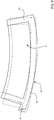
Figures 7 and 8 are schematic perspective views of a detail of the MEMS angular actuator ofFigure 2 , at rest and in use, respectively; -
Figure 9 is a schematic top view of the detail ofFigure 8 , wherein the rest position is identified by a dashed line; -
Figure 10 is a schematic top view of the detail ofFigure 4 , in use, wherein the rotation with respect to the rest position is identified by a dashed line; -
Figure 11 is a simplified perspective view of an optical shutter incorporating the present MEMS angular actuator, at rest; -
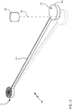
Figure 12 is a simplified perspective view of the optical shutter ofFigure 11 , in use; and -
Figures 13-18 are schematic cross-sections of the present MEMS angular actuator in successive manufacturing steps. - Described hereinbelow is an angular actuator 10 (also hereinafter referred to as actuator 10) made by thin-piezoelectric-film MEMS technology, capable of exerting a torque about an axis Z of a Cartesian reference system XYZ.
- As illustrated in
Figure 1 , theactuator 10 comprises asubstrate 11 of semiconductor material, for example silicon, and alayered structure 13 formed by a stack oflayers 17. - In detail, in this embodiment and as illustrated in
Figures 5 and6 , the stack oflayers 17 is formed by the succession, along the axis Z and from beneath upwards, of: a firstinsulating layer 20, for example of silicon oxide or tetraethyl orthosilicate (TEOS); astructural layer 21, of semiconductor material, for example silicon, having a large thickness, comprised, for example, between 50 µm and 500 µm (e.g. of approximately 300 pm); a secondinsulating layer 22, for example of silicon oxide or tetraethyl orthosilicate (TEOS); amembrane layer 23 of semiconductor material, for example polysilicon, having a thickness comprised, for example, between 0.2 µm and 50 µm (e.g. of approximately 0.7 pm); and a thirdinsulating layer 24, for example of silicon oxide or tetraethyl orthosilicate (TEOS). - The stack of
layers 17 is delimited at the top and at the bottom, respectively, by a top surface Stop and a bottom surface Sbot, which are formed, respectively, by the thirdinsulating layer 24 and the firstinsulating layer 20 and are parallel to the plane XY. - As illustrated in
Figures 2-4 , thelayered structure 13 is shaped, by agap 99, so as to form amain body 15, which comprises acentral portion 29A, having an approximately cylindrical shape, with axis OH parallel to the axis Z, and aperipheral portion 29B, which has a spiral shape and develops around thecentral portion 29A, and therefore about the axis OH. - As illustrated in
Figures 5 and6 , theactuator 10 further comprises apin 14, which extends underneath the bottom surface Sbot, and in particular underneath thecentral portion 29A, and has a cylindrical shape, with axis that coincides with the axis OH; moreover, thepin 14 has a first end bonded to thesubstrate 11 and a second end fixed to thecentral portion 29A. - In detail, the
pin 14 is formed by afirst portion 28A of semiconductor material, for example polysilicon, and asecond portion 28B of insulating material, such as silicon oxide or tetraethyl orthosilicate (TEOS). Thefirst portion 28A of thepin 14 is arranged underneath a portion of the firstinsulating layer 20 that forms thecentral portion 29A, in direct contact therewith; thesecond portion 28B of thepin 14 is arranged between thefirst portion 28A and thesubstrate 11, in direct contact therewith. - In practice, thanks to the presence of the
pin 14, theperipheral portion 29B of themain body 15 is suspended over thesubstrate 11, at a distance therefrom. - As mentioned previously, the
peripheral portion 29B of themain body 15 has a spiral shape, which comprises a plurality ofwindings 30 that extend in a concentric way from and around thecentral portion 29A, therefore about the axis OH. Themain body 15 has, at rest and in a direction parallel to the axis Y, a rest size D. In particular, assuming a cylindrical reference system centred on the axis OH and having a radial coordinate R and an angular coordinate θ, eachwinding 30 is formed by a corresponding part of theperipheral portion 29B of themain body 15 that has an extension equal to 360°, with respect to the angular coordinate θ. - Moreover, as described hereinafter in greater detail, the
windings 30 have, along the radial coordinate R, the same width; in addition, adjacent pairs of windings are set apart from one another by the same distance; in other words, theperipheral portion 29B of themain body 15 forms an Archimedean spiral. - In greater detail, the
windings 30 of theperipheral portion 29B of themain body 15 are formed by asupport structure 38* and by a plurality ofdeformable units 31 arranged in succession so as to form a single piece, starting from thecentral portion 29A, up to a finaldeformable unit 31A, which has the maximum distance (both in the radial direction and in the angular direction) from thecentral portion 29A. - Each
deformable unit 31 comprises amembrane 35, suspended over acorresponding cavity 37; arespective portion 38 of thesupport structure 38*; and a pair ofstiffening structures 39. - In greater detail, in each
deformable unit 31, themembrane 35 is formed by corresponding portions of the secondinsulating layer 22, of themembrane layer 23, and of the thirdinsulating layer 24. Moreover, thesupport structure 38* and thestiffening structures 39 are formed by corresponding portions of the firstinsulating layer 20 and of thestructural layer 21. - The
cavity 37 is delimited at the top by themembrane 35, is in part delimited laterally by therespective portion 38 of thesupport structure 38* and by thestiffening structures 39, is open at the bottom in the direction of theunderlying substrate 11 and laterally, in the direction of the axis OH, via a lateral opening AP (visible inFigure 7 ). - As illustrated in
Figure 5 , thesupport structure 38* is delimited laterally by an inner wall Pi, oriented towards the axis OH, and by an outer wall Pe, oriented outwards. - The inner wall Pi and the outer wall Pe wrap around the axis OH and are curved, with a single concavity oriented towards the axis OH. In addition, at each point of the inner wall Pi, the plane tangential to the inner wall Pi and passing through the point is parallel to the axis Z; the same consideration applies to the points of the outer wall Pe.
- To a first approximation, and at rest, the
portions 38 of thesupport structure 38* each have substantially, in top view, the shape of an annulus sector; therefore their sections perpendicular to the axis Z are invariant for translations along the axis Z. Furthermore, to a first approximation, the portions of outer wall Pe and inner wall Pi that delimit arespective portion 38 of thesupport structure 38* each have a respective single radius of curvature, the radius of curvature of the portion of outer wall Pe being greater than the radius of curvature of the portion of inner wall Pi. - The two
stiffening structures 39 have the same shape. In particular, eachstiffening structure 39 has the shape of a parallelepiped, which has a first end fixed to a respective end of therespective portion 38 of thesupport structure 38* (highlighted by a dashed line inFigure 6 ) and which extends therefrom, parallel to the direction of the radial coordinate and towards the axis OH, up to a second end. In other words, the second ends of thestiffening structures 39 are arranged at a shorter distance from the axis OH as compared to the corresponding first ends. - The
membranes 35 each overlie both therespective portion 38 of thesupport structure 38* and the respective pair ofstiffening structures 39, forming a single piece therewith. - Each
membrane 35 comprises afixed part 35A, fixed to the correspondingunderlying portion 38 of thesupport structure 38* and to the corresponding underlyingstiffening structures 39, and a suspendedpart 35B, which overlies therespective cavity 37. - In particular, as also visible in
Figure 7 , eachmembrane 35 has the shape, in top view, of a rectangle having curved long sides, whose two short sides and whose long side that is farther from the axis OH form thefixed part 35A and are fixed, respectively, to the twostiffening structures 39 and to thecorresponding portion 38 of thesupport structure 38*, whereas the long side closer to the axis OH is not constrained and forms anedge 36 that extends between the second ends of the correspondingstiffening structures 39, laterally delimiting the suspendedpart 35B of themembrane 35 and delimiting at the top the lateral opening AP of therespective cavity 37. - The
membranes 35 of thedeformable units 31 form a singleplanar structure 35*, without any discontinuity. - Without this implying any loss of generality, the
planar structure 35*, in addition to having a cross-section invariant with respect to translations along the axis Z, has a width, measured along the radial coordinate R, invariant with respect to the angular coordinate θ (and therefore also independent of the winding 30 considered), except for possible variations of width in the proximity of thecentral portion 29A, i.e. for values of θ lower, for example, than 270°. Moreover, theplanar structure 35* is laterally delimited by an inner surface Smi, oriented towards the axis OH, and an outer surface Sme, oriented outwards. The inner surface Smi and the outer surface Sme wrap around the axis OH. In addition, at each point of the inner surface Smi, the plane tangential to the inner surface Smi and passing through the point is parallel to the axis Z; the same consideration applies to the points of the outer surface Sme. - Each
membrane 35 is consequently formed by a portion of theplanar structure 35*. - In greater detail, the outer wall Pe is vertically aligned with the outer surface Sme of the
planar structure 35*. In other words, the outer wall Pe shares the generatrices with the outer surface Sme. - In addition, considering any pair formed by a first and a second winding 30 adjacent to one another, wherein the first winding 30 is arranged on the outside of the second winding 30, the portion of outer surface Sme of the second winding 30 and the portion of inner surface Smi of the first winding 30 are set apart from one another by a distance d (shown in
Figure 5 , for example equal to 145 µm) independent of the angular coordinate θ, and laterally delimit a corresponding portion of thegap 99, which, as mentioned previously, in top view, has a spiral shape and is arranged between pairs of adjacent windings. Furthermore, eachcavity 37 is laterally offset outwards with respect to the portion ofgap 99 that delimits thecorresponding membrane 35. All thecavities 37 are in fluid communication with thegap 99, since they are open laterally towards the axis OH. - The
deformable units 31 are arranged in succession, along a spiral profile, so as to form, as explained previously, thewindings 30 of themain body 15. - In detail, the pair of stiffening
structures 39 of the finaldeformable unit 31A comprises afinal stiffening structure 39A, having both angular and radial maximum distance with respect to the axis OH. - Moreover, as shown in
Figure 6 , and without this implying any loss of generality, the stiffeningstructures 39 have, in the radial direction, the same width, which, without this implying any loss of generality, is equal to the width of themembranes 35 and thus represents the width of thewindings 30. - A number of first units (e.g. nine in this embodiment) of the succession of
deformable units 31, arranged from thecentral portion 29A of themain body 15, may have shape and dimensions different from the remainingdeformable units 31. - In particular, in this embodiment, the
membrane 35 and the stiffeningstructures 39 of the first units of the succession ofdeformable units 31 have a smaller width with respect to the remainingdeformable units 31. - In addition, pairs of adjacent
deformable units 31 share acorresponding stiffening structure 39. - Again with reference to the
stiffening structures 39, and without this implying any loss of generality, at rest they are distributed angularly along twelve radial directions, angularly equally spaced, referred to hereinafter as the shared radial directions. In other words, except for the aforementioned firstdeformable units 31, the stiffeningstructures 39 of each winding 30 each extend along a respective shared radial direction. Consequently, the stiffeningstructures 39 may be grouped into groups, each group being associated to a corresponding shared radial direction and including, for each winding 30, the stiffeningstructure 39 of said winding 30 that extends in the corresponding shared radial direction. - The
actuator 10 further comprises a plurality ofactuation elements 40, each formed by a stack comprising abottom electrode 42 of metal material, for example platinum, anactuation region 43 of piezoelectric material, for example lead zirconate titanate (PZT), BaTiO3, KNN (sodium and potassium niobate), PbTiO2, or PbNb2O6 and having a thickness comprised between 1 µm and 3 µm, in particular of 2 µm, and atop electrode 44 of metal material, for example of a titanium-tungsten alloy; theactuation region 43 is arranged, in direct contact, between thebottom electrode 42 and thetop electrode 44. - Each
actuation element 40 is arranged on a respectivedeformable unit 31, and in particular on the portion of the third insulatinglayer 24 that forms the correspondingmembrane 35 so that therespective bottom electrode 42 contacts said portion of third insulatinglayer 24. Theactuation element 40 and the correspondingcavity 37 are therefore arranged on opposite sides of the correspondingmembrane 35. - In detail, without this implying any loss of generality, each
actuation element 40 overlies the suspendedpart 35B of therespective membrane 35. - Alternatively, embodiments (not illustrated) are possible wherein the
actuation elements 40 overlie also portions of thefixed part 35A of therespective membrane 35. - In greater detail, in this embodiment, only a part of the
deformable units 31 supports acorresponding actuation element 40. In particular, the aforementioned first units of the succession ofdeformable units 31 lack the correspondingactuation elements 40. However, embodiments are possible wherein all thedeformable units 31 supportrespective actuation elements 40. - Each
actuation element 40 is further coated by apassivation region 45 of insulating material, for example aluminium nitride, silicon nitride, undoped silicon glass (USG), hafnium oxide (HfO2), or dry polymeric film. - Alternatively, the
passivation region 45 may be formed by the superposition of a plurality of insulating layers. - In addition, the
top electrodes 44 of the plurality ofactuation elements 40 are connected together through a respective metal track, here not visible, which also enables the connection to contact pads, not visible, for the electrical connection to an external electrical biasi circuit. Likewise, thebottom electrodes 42 of the plurality ofactuation elements 40 are connected together through a respective metal track (here not visible), which also enables the connection to contact pads for the electrical connection to a suitable potential, for example to ground. - For instance, contact pads may be arranged on the
central portion 29A of themain body 15. - In use, a bias voltage is applied between the
top electrode 44 and thebottom electrode 42 of eachactuation element 40. In particular, the bias voltage may be a D.C. voltage or an A.C. voltage, according to the desired application. - The bias voltage causes, in each
actuation element 40, a deformation of thepiezoelectric region 43; consequently, eachmembrane 35, integral with respect to arespective actuation element 40, undergoes a deformation. - In particular, as may be seen in
Figure 8 (wherein the values of deformation have been amplified by a factor of one hundred for better clarity), starting from the portion offixed part 35A that overlies the correspondingportion 38 of thesupport structure 38* and moving along the radial direction towards the axis OH, the following occurs. The suspendedpart 35B of themembrane 35 initially curves towards thecavity 37, slightly below the corresponding rest position, so as to form a first concavity Cu facing upwards, and subsequently curves so as to rise markedly above the corresponding rest position, therefore in the direction opposite to thecavity 37, so as to form a second concavity CD facing downwards; in addition, theedge 36 curves and assumes a profile having a respective concavity, facing theunderlying cavity 37. - In detail, as may be seen in plan in
Figure 9 , wherein the rest position is highlighted by a dashed line and the deformed position by a solid line, the deformation of themembrane 35 is such as to cause a rototranslation, substantially in a direction parallel to the plane XY, of therespective stiffening structures 39 and of therespective portion 38 of thesupport structure 38*, the latter being also subject to a deformation. - In greater detail, the stiffening
structures 39 rotate, each about an own axis parallel to the axis Z, so that the second ends of the stiffeningstructures 39 of eachdeformable unit 31 move closer to each other; to a first approximation, such rotation is negligible. Furthermore, the stiffeningstructures 39 of eachdeformable unit 31 translate towards thecentral portion 29A of themain body 15. In addition, the stiffeningstructures 39 of eachdeformable unit 31 rotate, integrally to one another, around thecentral portion 29A of thecentral body 15, in the direction opposite to the winding direction of theperipheral portion 29B, said winding direction of theperipheral portion 29B being considered as starting from the finaldeformable unit 31A and in the direction of thecentral portion 29A. - The deformation of each
portion 38 of thesupport structure 38* is such that the curvature radiusesof the portions of the inner wall Pi and of the outer wall Pe that delimit eachportion 38 of thesupport structure 38* decrease as compared to the rest position. In other words, eachportion 38 of thesupport structure 38* increases, locally, its curvature, with consequent increase of the angular extension of thesupport structure 38*. - Each
deformable unit 31 thus undergoes a rotation, about the axis OH, the extent of such rotation increasing as the distance of thedeformable unit 31 from thecentral portion 29A increases; consequently, the finaldeformable unit 31A undergoes the rotation having maximum extent. - In particular, the
final stiffening structure 39A undergoes a maximum rotation, about the axis OH, with respect to the rest position. - Moreover, the
main body 15 undergoes a compression, parallel to the plane XY, so that themain body 15 assumes a work size D*, taken parallel to the axis Y, smaller than the rest size D. - In particular, the
final stiffening structure 39A may undergo a rotation, about the axis OH, by as much as 8° (as illustrated inFigure 10 by a dashed line with respect to the rest position), given a bias voltage of 40 V applied to theactuation elements 40. - In addition, the
main body 15, and in particular the finaldeformable unit 31A, undergoes a small out-of-plane displacement, parallel to the axis Z. In this embodiment, the out-of-plane displacement of thefinal stiffening structure 39A may be approximately 0.2% of its own displacement parallel to the plane XY, as verified by simulations made by the Applicant. In detail, such reduced out-of-plane displacement is obtained thanks to the large thickness of thesupport structure 38* and of the stiffeningstructures 39 with respect to the thickness of eachmembrane 35. - The
actuator 10 may be used in anoptical shutter 100, as shown inFigure 11 . - The
optical shutter 100 comprises, in addition to theactuator 10, anarm 101 and a blockingstructure 102. - The
arm 101 forms a single piece with the layeredstructure 13 and the blockingstructure 102 forms a single piece with thearm 101. Thearm 101 and the blockingstructure 102 are therefore formed by corresponding portions of the stack oflayers 17. - In detail, the
arm 101 has the shape of a parallelepiped having a thickness, along the axis Z, equal to the thickness of the stack oflayers 17 and a horizontal extension, parallel to the plane XY, that is relatively high, for example of the order of some millimetres. - The blocking
structure 102 here has a cylindrical shape, for example having a diameter of 1 mm and a thickness, parallel to the axis Z, equal to the thickness of the stack oflayers 17. - The blocking
structure 102 further comprises atop surface 104 coated with a material that absorbs or reflects electromagnetic radiation, such as a metal, for example gold or aluminium. - The
arm 101 is constrained, in this embodiment, at afirst end 101A, to thefinal stiffening structure 39A and to theportion 38 of thesupport structure 38* of the finaldeformable element 31A; moreover, asecond end 101B of thearm 101 is fixed to a portion of the lateral surface of the blockingstructure 102. - The
optical shutter 100 is arranged along an optical path of alight beam 105, for example of a laser type, generated by anoptical source 106. - Without this implying any loss of generality, the
optical shutter 100 is arranged so that, at rest, the blockingstructure 102 intercepts thelight beam 105, completely blocking the optical path. In particular, thelight beam 105 may be completely reflected or absorbed by thetop surface 104 of the blockingstructure 102. - In use, the bias voltage may cause a rotation of the
actuator 10, as previously discussed. - Consequently, as shown in
Figure 12 , the blockingstructure 102 moves with respect to the rest position (highlighted with a dashed line inFigure 12 ). - In particular, the blocking
structure 102 undergoes a rotation, whose arc has a linear length proportional to the rotation angle of thefinal stiffening structure 39A and to the length of thearm 101. - Therefore, the blocking
structure 102 frees the optical path of thelight beam 105. - The bias voltage may be applied so as to free the optical path of the
light beam 105 completely or partially, for example to modify the size and the intensity of thelight beam 105. - Alternatively, the bias voltage may have a frequency component that enables to modulate, in time, the intensity of the
light beam 105. - Advantageously, the
actuator 10 allows to obtain an optical shutter that has small dimensions, operates at low bias voltages, is efficient from the power consumption standpoint and has a small out-of-plane displacement of the blockingstructure 102. - Described hereinafter is the method for manufacturing the
actuator 10 ofFigure 1 . In particular, for clarity,Figures 13-18 show manufacturing steps regarding the cross-section taken along the line of section V-V. -
Figure 13 shows a cross-section of awafer 150 that has already undergone first manufacturing steps. In detail, thewafer 150 comprises a work substrate 151 (intended to form thestructural layer 21 of the stack of layers 17) of semiconductor material, for example silicon, having afirst surface 151A and asecond surface 151B. Thework substrate 151 has already undergone grinding and polishing, for example through chemical-mechanical polishing (CMP), so to obtain a thickness of, for example, 300 µm. - A first dielectric layer 152 (intended to form the second insulating
layer 22 of the stack of layers 17), for example of deposited tetraethyl orthosilicate (TEOS) and havinga thickness of, for example, at least 1 µm, here 1 µm, extends over thefirst surface 151A of thework substrate 151. - A passive layer 153 (intended to form the
membrane layer 22 of the stack of layers 17) of semiconductor material, for example polysilicon and here having a thickness of 700 nm, extends over thefirst dielectric layer 152. - A second dielectric layer 154 (intended to form the third insulating
layer 24 of the stack of layers 17), for example of deposited TEOS and having a thickness of, for example, 0.5 µm, extending over thepassive layer 153. - A first patterning layer 155 (intended to form the first insulating
layer 20 of the stack of layers 17), for example of TEOS and having a thickness of, for example, 1 µm, extends over thesecond surface 151B of thework substrate 151; abonding layer 156 of semiconductor material, for example polysilicon, and having a thickness of, for example, 50 µm extends underneath thefirst patterning layer 155, in direct contact therewith. - Next,
Figure 14 , afirst metal layer 160, for example of platinum, is deposited on thesecond dielectric layer 154; anactuation layer 161 of piezoelectric material, for example titanium lead-zirconate (PZT), BaTiO3, KNN (sodium and potassium niobate), PbTiO2, or PbNb2O6 and having a thickness comprised between 1 µm and 3 µm, in particular of 2 µm, is deposited on thefirst metal layer 160; asecond metal layer 162, for example of a tungsten-titanium alloy, is deposited on theactuation layer 161, forming a stack of actuation layers. - The stack of actuation layers thus obtained is defined by lithographic steps and selective chemical etching so as to form the plurality of
actuation elements 40. - In particular, for each
actuation element 40, thefirst metal layer 160 forms thebottom electrode 42, theactuation layer 161 forms theactuation region 43, and thesecond metal layer 162 forms thetop electrode 44. - In addition, the
first metal layer 160 also forms a respective metal track, here not illustrated, for the mutual electrical connection and the electrical connection with respective contact pads of eachbottom electrode 42 of theactuation elements 40. - In addition, a
passivation layer 163, of insulating material such as aluminium nitride, silicon nitride, undoped silicon glass (USG), hafnium oxide (HfO2), or dry polymeric film, is deposited so as to cover completely and surround theactuation elements 40 and is defined lithographically so as to form, for eachactuation element 40, thepassivation region 45. - Next, in a way not illustrated but known to the person skilled in the art, a via is formed in each
passivation region 45, and a further metal layer is deposited on theactuation elements 40 and defined so as to form a respective metal track, here not illustrated, for mutual electrical connection and electrical connection with respective contact pads, of eachtop electrode 44. - As illustrated in
Figure 15 , thewafer 150 then undergoes a sequence of selective chemical etchings from thesecond dielectric layer 154 and as far as thefirst surface 151A of thework substrate 151 so as to form atrench 165 and expose a part of thework substrate 151. Thetrench 165 extends, along the axis Z, through thesecond dielectric layer 154, thepassive layer 153 and thefirst dielectric layer 152, as far as thefirst surface 151A of thework substrate 151; in top view, thetrench 165 has a spiral shape and is designed to form thegap 99. In particular, as may be seen inFigure 15 , thetrench 165 is laterally offset with respect to eachactuation element 40. - Next, as illustrated in
Figure 16 , thebond layer 156 undergoes grinding and chemical-mechanical polishing, to obtain a thickness of, for example, 4 µm. - A
second patterning layer 170 is then deposited on thebond layer 156 and is defined lithographically so as to form awindow 171. Thewindow 171 extends through thepatterning layer 170 so as to expose part of thebond layer 156. From thesecond patterning layer 170, aportion 172 remains, which is shaped approximately like a cylinder having, as axis, the axis OH and is intended to form thesecond portion 28B of thepin 14. - Next,
Figure 17 , selective chemical etchings are performed on thesecond surface 151B of thework substrate 151, by using theportion 172 of thesecond patterning layer 170, so as to form thecavities 37 and themain body 15. - In detail, the
window 171 is used to selectively remove part of thebonding layer 156, of which a portion remains, arranged on top of theportion 172 of the second insulating layer, intended to form thefirst portion 28A of thepin 14. - Next, the
first patterning layer 155 is defined lithographically so as to form a portion arranged on top of the remaining portion of the bonding layer 156 (intended to form thesecond portion 28B of the pin 14), and a plurality ofportions 173 laterally offset, so as to leave exposed portions of thesecond surface 151B of thework substrate 151. Next, using theportion 172 of thesecond patterning layer 170 and the plurality ofportions 173 of thefirst patterning layer 155 as mask, portions of thework substrate 151 are removed selectively, from the exposed portions of thesecond surface 151B and as far as thefirst surface 151A of thework substrate 151 so as to form the correspondingcavities 37, which communicate with thetrench 165. - In this way, in addition to the
cavity 37, thepin 14, thesupport structure 38*, themembranes 35 and the stiffeningstructures 39 of eachdeformable unit 31 are formed. - Next,
Figure 18 , theportion 172 of thesecond patterning layer 170 is bonded to asupport wafer 180 of semiconductor material, for example silicon. - Finally, in a way not illustrated, the
group 200 formed by thewafer 150 and thesupport wafer 180 are diced so that, after per se known operations of packaging and electrical connection, each die forms theactuator 10 ofFigure 1 . In detail, thesupport wafer 180 forms thesubstrate 11. - The methods described herein may be extended, in a per se known manner to the person skilled in the art, for manufacturing, from the
wafer 150, also thearm 101 and the blockingstructure 102 of theoptical shutter 100. - Finally, it is clear that modifications and variations may be made to the
actuator 10, theoptical shutter 100, and the manufacturing method described and illustrated herein, without thereby departing from the scope of the present invention, as defined in the annexed claims. - For instance, the windings of the peripheral portion of the main body formed by the layered structure may be spaced apart by a variable distance, for example to form a logarithmic spiral. However, a variable distance between the windings may involve the use of a greater area of material given the same performance of the MEMS angular actuator.
- For instance, the number of windings, the size of the windings, the number of deformable units, the number of actuation elements and the thickness of each layer of the stack of layers may be modified and chosen based on the desired mechanical properties of the MEMS angular actuator.
- For instance, the stiffening structures may extend, starting outwards from the corresponding portion of the support structure, i.e. moving away from the central portion of the main body so that the cavities and the lateral openings of the deformable units are oriented outwards and not towards the central portion of the main body.
- For instance, the actuation elements may extend partially on the portion of the support structure and/or at least part of the pair of stiffening structures of each deformable unit.
- For instance, each deformable unit may have a respective pair of stiffening structures distinct from the pair of stiffening structures of an adjacent deformable unit.
- For instance, the arm of the shutter may be constrained to any stiffening structure or portion of support structure of any deformable unit.
- It will moreover be evident to the person skilled in the art that the peripheral portion of the central body may have portions, for small values of the angular coordinate θ and therefore in the proximity of the central portion of the main body, which have shapes and dimensions that differ from the shapes and dimensions of corresponding portions for higher values of the angular coordinate θ, on account of specific manufacturing requirements.
Claims (14)
- A MEMS actuator (10) comprising a main body (15) including a central portion (29A), couplable to a substrate (11), and a peripheral portion (29B), which, when said central portion (29A) is coupled to said substrate (11), is suspended over the substrate and comprises a deformable structure (35*), which at rest has a spiral planar shape, extends around the central portion (29A), and forms a plurality of membranes (35) arranged in succession;
said MEMS actuator (10) further comprising:- a plurality of bearing structures (38, 39), each bearing structure (38, 39) being fixed at the top to the deformable structure (35*) and laterally delimiting a corresponding cavity (37), which has a lateral opening (AP) facing the central portion (29A) of the main body (15) and is closed at the top by a corresponding membrane (35), said corresponding membrane (35) comprising a fixed part (35A), fixed to the underlying bearing structure (38, 39), and a suspended part (35B), which is laterally offset with respect to the underlying bearing structure (38, 39) and delimits at the top said lateral opening (AP) of the cavity (37);- for each bearing structure (38, 39), a corresponding piezoelectric actuator (40);and wherein the piezoelectric actuators (40) are electrically controllable so as to cause, each, a deformation of the corresponding membrane (35), the deformation comprising a curving upwards of a portion (36) of the suspended part (35B), the curvings of the portions (36) of the suspended parts (35B) of the membranes (35) causing a rotation of the bearing structures (38, 39) around the central portion (29A) of the main body (15). - The actuator according to claim 1, further comprising a support structure (38*), which has a spiral shape and extends underneath the deformable structure (35*); and wherein each bearing structure (38, 39) comprises:- a corresponding portion (38) of the support structure (38*); and- a pair of stiffening structures (39), which, at rest, extend from corresponding ends of the corresponding portion (38) of the support structure (38*), along corresponding radial directions, towards the central portion (29A) of the main body (15);and wherein the fixed part (35A) of each membrane (35) is fixed to the corresponding pair of stiffening structures (39) and to the corresponding portion (38) of the support structure (38*); and wherein the curvings of the portions (36) of the suspended parts (35B) of the membranes (35) cause an increase of the curvature of each portion (38) of the support structure (38*), with consequent increase of the angular extension of the support structure (38*) and rototranslation of the stiffening structures (39), said rototranslation comprising a rotation around the central portion (29A) of the main body (15).
- The actuator according to claim 2, wherein each stiffening structure (39) has a first end, integral with the corresponding portion (38) of support structure (38*) and a second end; and wherein the suspended part (35B) of each membrane (35) comprises a respective edge (36), which extends between the second ends of the corresponding stiffening structures (39) and overlies the corresponding lateral opening (AP), which is laterally delimited by the second ends of the corresponding stiffening structures (39); and wherein the curving of the portion (36) of the suspended part (35B) of each membrane (35) causes a curving upwards of the corresponding edge (36), with concavity facing downwards.
- The actuator according to claim 3, wherein the membranes (35) have a dimension along the radial direction that is angularly invariant.
- The actuator according to claim 3 or claim 4, wherein at least part of the support structure (38*) has a dimension along the radial direction that is angularly invariant.
- The actuator according to any of claims 2 to 5, wherein the deformable structure (35*) has a thickness smaller than the thickness of the stiffening structures (39) and of the support structure (38*).
- The actuator according to any of the preceding claims, wherein each piezoelectric actuator (40) comprises a piezoelectric region (43), which extends over the suspended part (35B) of the corresponding membrane (35).
- An optical shutter (100) comprising:- the MEMS actuator (10) according to any of the preceding claims;- an arm (101) having a first end (101A) and a second end (101B), the first end being constrained to one of said bearing structures (38, 39); and- a blocking structure (102) constrained to the second end (101B) of the arm (101) and configured to reflect or absorb electromagnetic radiation.
- The optical shutter (100) according to claim 8, wherein said arm (101) is constrained to the bearing structure (38, 39) which is the most distant from said central portion (29A) of the main body (15).
- A system comprising:- an optical shutter (100) according to claim 8 or claim 9; and- an optical source (106) configured to generate an optical beam (105);and wherein the optical shutter (100) is configured to operate alternatively in:- a first operating condition, wherein said optical beam (105) impinges upon said blocking structure (102); and- a second operating condition, wherein said optical beam (105) is at least partially offset laterally with respect to the blocking structure (102).
- A method for manufacturing a MEMS actuator (10) comprising the steps of:- forming a main body (15) including a central portion (29A), couplable to a substrate (11), and a peripheral portion (29B), which, when said central portion (29A) is coupled to said substrate (11), is suspended over the substrate and comprises a deformable structure (35*), which at rest has a spiral planar shape, extends around the central portion (29A) and forms a plurality of membranes (35) arranged in succession;- forming a plurality of bearing structures (38, 39), each bearing structure (38, 39) being fixed at the top of the deformable structure (35*) and laterally delimiting a corresponding cavity (37), which has a lateral opening (AP) facing the central portion (29A) of the main body (15) and is closed at the top by a corresponding membrane (35), said corresponding membrane (35) comprising a fixed part (35A), fixed to the underlying bearing structure (38, 39), and a suspended part (35B), which is laterally offset with respect to the underlying bearing structure (38, 39) and delimits at the top said lateral opening (AP) of the cavity (37); and- for each bearing structure (38, 39), forming a corresponding piezoelectric actuator (40), said piezoelectric actuators (40) being electrically controllable so as to cause, each, a deformation of the corresponding membrane (35), the deformation comprising a curving upwards of a portion (36) of the suspended part (35B), the curvings of the portions (36) of the suspended parts (35B) of the membranes (35) causing a rotation of the bearing structures (38, 39) around the central portion (29A) of the main body (15) .
- The manufacturing method according to claim 11, further comprising the step of:- forming a support structure (38*), which has a spiral shape and extends underneath the deformable structure (35*);and wherein said step of forming a plurality of bearing structures (38, 39) comprises:- forming each bearing structure (38, 39) so as to include a corresponding portion (38) of the support structure (38*); and- for each bearing structure (38, 39), forming a pair of stiffening structures (39), which, at rest, extend from corresponding ends of the corresponding portion (38) of the support structure (38*), along corresponding radial directions, towards the central portion (29A) of the main body (15);and wherein said step of forming a main body (15) is such that the fixed part (35A) of each membrane (35) is fixed to the corresponding pair of stiffening structures (39) and to the corresponding portion (38) of the support structure (38*), so that the curvings of the portions (36) of the suspended parts (35B) of the membranes (35) cause an increase of the curvature of each portion (38) of the support structure (38*), with consequent increase of the angular extension of the support structure (38*) and rototranslation of the stiffening structures (39), said rototranslation comprising a rotation around the central portion (29A) of the main body (15).
- The manufacturing method according to claim 12, wherein said step of forming a main body (15) comprises:- forming, on a semiconductor substrate (151) delimited by a front surface (151A) and by a rear face (151B), a multilayer dielectric structure (152, 153, 154), and subsequently performing said step of forming the piezoelectric actuators (40), on the multilayer dielectric structure (152, 153, 154);- selectively removing portions of the multilayer dielectric structure (152, 153, 154) laterally offset with respect to said piezoelectric actuators (40), so as to form a trench (165) of spiral shape, which faces the semiconductor substrate (151) and laterally delimits said deformable structure (35*);and wherein said step of forming a plurality of bearing structures (38, 39) comprises:- selectively removing portions of the semiconductor substrate (151), from the rear face (151B), so that said cavities (27) communicate with the trench (165).
- The manufacturing method according to claim 13, further comprising the step of:- after performing said step of selectively removing portions of the semiconductor substrate (151), fixing the central portion (29A) of the main body (15) to a semiconductor wafer (180), so that the peripheral portion (29B) of the main body (15) is suspended over the semiconductor wafer (180).
Applications Claiming Priority (1)
| Application Number | Priority Date | Filing Date | Title |
|---|---|---|---|
| IT102020000015775A IT202000015775A1 (en) | 2020-06-30 | 2020-06-30 | PIEZOELECTRIC ANGULAR ACTUATOR FOR A MEMS SHUTTER AND ITS MANUFACTURING METHOD |
Publications (2)
| Publication Number | Publication Date |
|---|---|
| EP3933460A1 true EP3933460A1 (en) | 2022-01-05 |
| EP3933460B1 EP3933460B1 (en) | 2023-04-19 |
Family
ID=72356425
Family Applications (1)
| Application Number | Title | Priority Date | Filing Date |
|---|---|---|---|
| EP21182607.8A Active EP3933460B1 (en) | 2020-06-30 | 2021-06-29 | Angular piezoelectric actuator for a mems shutter and manufacturing method thereof |
Country Status (3)
| Country | Link |
|---|---|
| US (1) | US12117605B2 (en) |
| EP (1) | EP3933460B1 (en) |
| IT (1) | IT202000015775A1 (en) |
Families Citing this family (4)
| Publication number | Priority date | Publication date | Assignee | Title |
|---|---|---|---|---|
| IT202000010264A1 (en) * | 2020-05-07 | 2021-11-07 | St Microelectronics Srl | PIEZOELECTRIC ACTUATOR HAVING A DEFORMATION SENSOR AND RELATED MANUFACTURING PROCEDURE |
| IT202000010261A1 (en) | 2020-05-07 | 2021-11-07 | St Microelectronics Srl | PIEZOELECTRIC ACTUATOR EQUIPPED WITH A DEFORMABLE STRUCTURE HAVING IMPROVED MECHANICAL PROPERTIES AND RELATED MANUFACTURING PROCEDURE |
| US11800297B2 (en) | 2020-12-16 | 2023-10-24 | Invensense, Inc. | Reduced light reflection package |
| CN116438807A (en) | 2020-12-16 | 2023-07-14 | 应美盛股份有限公司 | Light reflection reducing package |
Citations (1)
| Publication number | Priority date | Publication date | Assignee | Title |
|---|---|---|---|---|
| GB2379746A (en) * | 2001-09-18 | 2003-03-19 | Marconi Caswell Ltd | Shutter assembly for telecommunication networks |
Family Cites Families (3)
| Publication number | Priority date | Publication date | Assignee | Title |
|---|---|---|---|---|
| US7753491B2 (en) * | 1997-07-15 | 2010-07-13 | Silverbrook Research Pty Ltd | Printhead nozzle arrangement incorporating a corrugated electrode |
| SG10201407632UA (en) * | 2013-11-26 | 2015-06-29 | Agency Science Tech & Res | Transducer and method for forming the same |
| EP3754733B1 (en) * | 2019-06-19 | 2026-05-20 | Univ Freiburg Albert Ludwigs | Piezoelectric actuator and microfluidic device |
-
2020
- 2020-06-30 IT IT102020000015775A patent/IT202000015775A1/en unknown
-
2021
- 2021-06-23 US US17/355,861 patent/US12117605B2/en active Active
- 2021-06-29 EP EP21182607.8A patent/EP3933460B1/en active Active
Patent Citations (1)
| Publication number | Priority date | Publication date | Assignee | Title |
|---|---|---|---|---|
| GB2379746A (en) * | 2001-09-18 | 2003-03-19 | Marconi Caswell Ltd | Shutter assembly for telecommunication networks |
Non-Patent Citations (2)
| Title |
|---|
| SADAT S H ET AL: "Large-Deflection Spiral-Shaped Micromirror Actuator", JOURNAL OF MICROELECTROMECHANICAL SYSTEMS, IEEE SERVICE CENTER, US, vol. 18, no. 6, 1 December 2009 (2009-12-01), pages 1357 - 1364, XP011283834, ISSN: 1057-7157, DOI: 10.1109/JMEMS.2009.2031700 * |
| SADAT, S. H. ET AL.: "Journal of Microelectromechanical Systems", vol. 18, December 2009, IEEE SERVICE CENTER, article "Large-Deflection Spiral-Shaped Micromirror Actuator", pages: 1357 - 1364 |
Also Published As
| Publication number | Publication date |
|---|---|
| US12117605B2 (en) | 2024-10-15 |
| US20210405346A1 (en) | 2021-12-30 |
| IT202000015775A1 (en) | 2021-12-30 |
| EP3933460B1 (en) | 2023-04-19 |
Similar Documents
| Publication | Publication Date | Title |
|---|---|---|
| EP3933460B1 (en) | Angular piezoelectric actuator for a mems shutter and manufacturing method thereof | |
| US11807517B2 (en) | MEMS device comprising a membrane and an actuator | |
| US8691099B2 (en) | Process for fabricating MEMS devices | |
| US7872394B1 (en) | MEMS device with two axes comb drive actuators | |
| AU774240B2 (en) | Microelectromechanical optical switch and method of manufacture thereof | |
| US6686639B1 (en) | High performance MEMS device fabricatable with high yield | |
| US6995495B2 (en) | 2-D actuator and manufacturing method thereof | |
| TWI411064B (en) | Microelectromechanical system | |
| EP3236304B1 (en) | A scanning mirror device and a method for manufacturing it | |
| US20040060898A1 (en) | Process for high yield fabrication of MEMS devices | |
| CN101284642A (en) | Micromechanical Devices with Tilted Electrodes | |
| US7986073B2 (en) | Micro-electro mechanical system using snapping tabs, comb and parallel plate actuation | |
| JP2010525377A (en) | Micro mirror for micro electro mechanical system | |
| Hah et al. | A self-aligned vertical comb-drive actuator on an SOI wafer for a 2D scanning micromirror | |
| US6433390B1 (en) | Bonded substrate structures and method for fabricating bonded substrate structures | |
| JP2017211576A (en) | Optical deflector and manufacturing method therefor | |
| CN113860253B (en) | Angular piezoelectric actuator for MEMS shutter and manufacturing method thereof | |
| EP4187289A1 (en) | Micro-electro-mechanical optical shutter with rotating shielding structures and related manufacturing process | |
| KR20020086972A (en) | A micromirror actuator | |
| US6654155B2 (en) | Single-crystal-silicon ribbon hinges for micro-mirror and MEMS assembly on SOI material | |
| US9676609B2 (en) | Integrated MEMS device | |
| CN104167433A (en) | Device comprising a spring and an element suspended thereon, and method for manufacturing same | |
| Martini et al. | Andromeda: A Flexible MEMS Technology Platform for a Variety of Piezoelectrically Actuacted Micromirrors |
Legal Events
| Date | Code | Title | Description |
|---|---|---|---|
| PUAI | Public reference made under article 153(3) epc to a published international application that has entered the european phase |
Free format text: ORIGINAL CODE: 0009012 |
|
| STAA | Information on the status of an ep patent application or granted ep patent |
Free format text: STATUS: THE APPLICATION HAS BEEN PUBLISHED |
|
| AK | Designated contracting states |
Kind code of ref document: A1 Designated state(s): AL AT BE BG CH CY CZ DE DK EE ES FI FR GB GR HR HU IE IS IT LI LT LU LV MC MK MT NL NO PL PT RO RS SE SI SK SM TR |
|
| B565 | Issuance of search results under rule 164(2) epc |
Effective date: 20211129 |
|
| STAA | Information on the status of an ep patent application or granted ep patent |
Free format text: STATUS: REQUEST FOR EXAMINATION WAS MADE |
|
| 17P | Request for examination filed |
Effective date: 20220603 |
|
| RBV | Designated contracting states (corrected) |
Designated state(s): AL AT BE BG CH CY CZ DE DK EE ES FI FR GB GR HR HU IE IS IT LI LT LU LV MC MK MT NL NO PL PT RO RS SE SI SK SM TR |
|
| GRAP | Despatch of communication of intention to grant a patent |
Free format text: ORIGINAL CODE: EPIDOSNIGR1 |
|
| STAA | Information on the status of an ep patent application or granted ep patent |
Free format text: STATUS: GRANT OF PATENT IS INTENDED |
|
| RIC1 | Information provided on ipc code assigned before grant |
Ipc: G02B 26/04 20060101ALI20221010BHEP Ipc: G02B 26/02 20060101ALI20221010BHEP Ipc: G02B 5/00 20060101AFI20221010BHEP |
|
| INTG | Intention to grant announced |
Effective date: 20221110 |
|
| GRAS | Grant fee paid |
Free format text: ORIGINAL CODE: EPIDOSNIGR3 |
|
| GRAA | (expected) grant |
Free format text: ORIGINAL CODE: 0009210 |
|
| STAA | Information on the status of an ep patent application or granted ep patent |
Free format text: STATUS: THE PATENT HAS BEEN GRANTED |
|
| AK | Designated contracting states |
Kind code of ref document: B1 Designated state(s): AL AT BE BG CH CY CZ DE DK EE ES FI FR GB GR HR HU IE IS IT LI LT LU LV MC MK MT NL NO PL PT RO RS SE SI SK SM TR |
|
| REG | Reference to a national code |
Ref country code: GB Ref legal event code: FG4D |
|
| REG | Reference to a national code |
Ref country code: DE Ref legal event code: R096 Ref document number: 602021001947 Country of ref document: DE |
|
| REG | Reference to a national code |
Ref country code: CH Ref legal event code: EP |
|
| REG | Reference to a national code |
Ref country code: IE Ref legal event code: FG4D |
|
| REG | Reference to a national code |
Ref country code: AT Ref legal event code: REF Ref document number: 1561613 Country of ref document: AT Kind code of ref document: T Effective date: 20230515 |
|
| REG | Reference to a national code |
Ref country code: LT Ref legal event code: MG9D |
|
| REG | Reference to a national code |
Ref country code: NL Ref legal event code: MP Effective date: 20230419 |
|
| REG | Reference to a national code |
Ref country code: AT Ref legal event code: MK05 Ref document number: 1561613 Country of ref document: AT Kind code of ref document: T Effective date: 20230419 |
|
| PG25 | Lapsed in a contracting state [announced via postgrant information from national office to epo] |
Ref country code: NL Free format text: LAPSE BECAUSE OF FAILURE TO SUBMIT A TRANSLATION OF THE DESCRIPTION OR TO PAY THE FEE WITHIN THE PRESCRIBED TIME-LIMIT Effective date: 20230419 |
|
| PG25 | Lapsed in a contracting state [announced via postgrant information from national office to epo] |
Ref country code: SE Free format text: LAPSE BECAUSE OF FAILURE TO SUBMIT A TRANSLATION OF THE DESCRIPTION OR TO PAY THE FEE WITHIN THE PRESCRIBED TIME-LIMIT Effective date: 20230419 Ref country code: PT Free format text: LAPSE BECAUSE OF FAILURE TO SUBMIT A TRANSLATION OF THE DESCRIPTION OR TO PAY THE FEE WITHIN THE PRESCRIBED TIME-LIMIT Effective date: 20230821 Ref country code: NO Free format text: LAPSE BECAUSE OF FAILURE TO SUBMIT A TRANSLATION OF THE DESCRIPTION OR TO PAY THE FEE WITHIN THE PRESCRIBED TIME-LIMIT Effective date: 20230719 Ref country code: ES Free format text: LAPSE BECAUSE OF FAILURE TO SUBMIT A TRANSLATION OF THE DESCRIPTION OR TO PAY THE FEE WITHIN THE PRESCRIBED TIME-LIMIT Effective date: 20230419 Ref country code: AT Free format text: LAPSE BECAUSE OF FAILURE TO SUBMIT A TRANSLATION OF THE DESCRIPTION OR TO PAY THE FEE WITHIN THE PRESCRIBED TIME-LIMIT Effective date: 20230419 |
|
| PG25 | Lapsed in a contracting state [announced via postgrant information from national office to epo] |
Ref country code: RS Free format text: LAPSE BECAUSE OF FAILURE TO SUBMIT A TRANSLATION OF THE DESCRIPTION OR TO PAY THE FEE WITHIN THE PRESCRIBED TIME-LIMIT Effective date: 20230419 Ref country code: PL Free format text: LAPSE BECAUSE OF FAILURE TO SUBMIT A TRANSLATION OF THE DESCRIPTION OR TO PAY THE FEE WITHIN THE PRESCRIBED TIME-LIMIT Effective date: 20230419 Ref country code: LV Free format text: LAPSE BECAUSE OF FAILURE TO SUBMIT A TRANSLATION OF THE DESCRIPTION OR TO PAY THE FEE WITHIN THE PRESCRIBED TIME-LIMIT Effective date: 20230419 Ref country code: LT Free format text: LAPSE BECAUSE OF FAILURE TO SUBMIT A TRANSLATION OF THE DESCRIPTION OR TO PAY THE FEE WITHIN THE PRESCRIBED TIME-LIMIT Effective date: 20230419 Ref country code: IS Free format text: LAPSE BECAUSE OF FAILURE TO SUBMIT A TRANSLATION OF THE DESCRIPTION OR TO PAY THE FEE WITHIN THE PRESCRIBED TIME-LIMIT Effective date: 20230819 Ref country code: HR Free format text: LAPSE BECAUSE OF FAILURE TO SUBMIT A TRANSLATION OF THE DESCRIPTION OR TO PAY THE FEE WITHIN THE PRESCRIBED TIME-LIMIT Effective date: 20230419 Ref country code: GR Free format text: LAPSE BECAUSE OF FAILURE TO SUBMIT A TRANSLATION OF THE DESCRIPTION OR TO PAY THE FEE WITHIN THE PRESCRIBED TIME-LIMIT Effective date: 20230720 Ref country code: AL Free format text: LAPSE BECAUSE OF FAILURE TO SUBMIT A TRANSLATION OF THE DESCRIPTION OR TO PAY THE FEE WITHIN THE PRESCRIBED TIME-LIMIT Effective date: 20230419 |
|
| PG25 | Lapsed in a contracting state [announced via postgrant information from national office to epo] |
Ref country code: FI Free format text: LAPSE BECAUSE OF FAILURE TO SUBMIT A TRANSLATION OF THE DESCRIPTION OR TO PAY THE FEE WITHIN THE PRESCRIBED TIME-LIMIT Effective date: 20230419 |
|
| PG25 | Lapsed in a contracting state [announced via postgrant information from national office to epo] |
Ref country code: SK Free format text: LAPSE BECAUSE OF FAILURE TO SUBMIT A TRANSLATION OF THE DESCRIPTION OR TO PAY THE FEE WITHIN THE PRESCRIBED TIME-LIMIT Effective date: 20230419 |
|
| PG25 | Lapsed in a contracting state [announced via postgrant information from national office to epo] |
Ref country code: MC Free format text: LAPSE BECAUSE OF FAILURE TO SUBMIT A TRANSLATION OF THE DESCRIPTION OR TO PAY THE FEE WITHIN THE PRESCRIBED TIME-LIMIT Effective date: 20230419 |
|
| REG | Reference to a national code |
Ref country code: DE Ref legal event code: R097 Ref document number: 602021001947 Country of ref document: DE |
|
| PG25 | Lapsed in a contracting state [announced via postgrant information from national office to epo] |
Ref country code: SM Free format text: LAPSE BECAUSE OF FAILURE TO SUBMIT A TRANSLATION OF THE DESCRIPTION OR TO PAY THE FEE WITHIN THE PRESCRIBED TIME-LIMIT Effective date: 20230419 Ref country code: SK Free format text: LAPSE BECAUSE OF FAILURE TO SUBMIT A TRANSLATION OF THE DESCRIPTION OR TO PAY THE FEE WITHIN THE PRESCRIBED TIME-LIMIT Effective date: 20230419 Ref country code: RO Free format text: LAPSE BECAUSE OF FAILURE TO SUBMIT A TRANSLATION OF THE DESCRIPTION OR TO PAY THE FEE WITHIN THE PRESCRIBED TIME-LIMIT Effective date: 20230419 Ref country code: MC Free format text: LAPSE BECAUSE OF FAILURE TO SUBMIT A TRANSLATION OF THE DESCRIPTION OR TO PAY THE FEE WITHIN THE PRESCRIBED TIME-LIMIT Effective date: 20230419 Ref country code: EE Free format text: LAPSE BECAUSE OF FAILURE TO SUBMIT A TRANSLATION OF THE DESCRIPTION OR TO PAY THE FEE WITHIN THE PRESCRIBED TIME-LIMIT Effective date: 20230419 Ref country code: DK Free format text: LAPSE BECAUSE OF FAILURE TO SUBMIT A TRANSLATION OF THE DESCRIPTION OR TO PAY THE FEE WITHIN THE PRESCRIBED TIME-LIMIT Effective date: 20230419 Ref country code: CZ Free format text: LAPSE BECAUSE OF FAILURE TO SUBMIT A TRANSLATION OF THE DESCRIPTION OR TO PAY THE FEE WITHIN THE PRESCRIBED TIME-LIMIT Effective date: 20230419 |
|
| PLBE | No opposition filed within time limit |
Free format text: ORIGINAL CODE: 0009261 |
|
| STAA | Information on the status of an ep patent application or granted ep patent |
Free format text: STATUS: NO OPPOSITION FILED WITHIN TIME LIMIT |
|
| REG | Reference to a national code |
Ref country code: BE Ref legal event code: MM Effective date: 20230630 |
|
| PG25 | Lapsed in a contracting state [announced via postgrant information from national office to epo] |
Ref country code: LU Free format text: LAPSE BECAUSE OF NON-PAYMENT OF DUE FEES Effective date: 20230629 |
|
| 26N | No opposition filed |
Effective date: 20240122 |
|
| REG | Reference to a national code |
Ref country code: IE Ref legal event code: MM4A |
|
| PG25 | Lapsed in a contracting state [announced via postgrant information from national office to epo] |
Ref country code: LU Free format text: LAPSE BECAUSE OF NON-PAYMENT OF DUE FEES Effective date: 20230629 |
|
| PG25 | Lapsed in a contracting state [announced via postgrant information from national office to epo] |
Ref country code: IE Free format text: LAPSE BECAUSE OF NON-PAYMENT OF DUE FEES Effective date: 20230629 |
|
| PG25 | Lapsed in a contracting state [announced via postgrant information from national office to epo] |
Ref country code: IE Free format text: LAPSE BECAUSE OF NON-PAYMENT OF DUE FEES Effective date: 20230629 |
|
| PG25 | Lapsed in a contracting state [announced via postgrant information from national office to epo] |
Ref country code: SI Free format text: LAPSE BECAUSE OF FAILURE TO SUBMIT A TRANSLATION OF THE DESCRIPTION OR TO PAY THE FEE WITHIN THE PRESCRIBED TIME-LIMIT Effective date: 20230419 |
|
| PG25 | Lapsed in a contracting state [announced via postgrant information from national office to epo] |
Ref country code: SI Free format text: LAPSE BECAUSE OF FAILURE TO SUBMIT A TRANSLATION OF THE DESCRIPTION OR TO PAY THE FEE WITHIN THE PRESCRIBED TIME-LIMIT Effective date: 20230419 Ref country code: IT Free format text: LAPSE BECAUSE OF FAILURE TO SUBMIT A TRANSLATION OF THE DESCRIPTION OR TO PAY THE FEE WITHIN THE PRESCRIBED TIME-LIMIT Effective date: 20230419 Ref country code: FR Free format text: LAPSE BECAUSE OF NON-PAYMENT OF DUE FEES Effective date: 20230630 Ref country code: BE Free format text: LAPSE BECAUSE OF NON-PAYMENT OF DUE FEES Effective date: 20230630 |
|
| PG25 | Lapsed in a contracting state [announced via postgrant information from national office to epo] |
Ref country code: BG Free format text: LAPSE BECAUSE OF FAILURE TO SUBMIT A TRANSLATION OF THE DESCRIPTION OR TO PAY THE FEE WITHIN THE PRESCRIBED TIME-LIMIT Effective date: 20230419 |
|
| PG25 | Lapsed in a contracting state [announced via postgrant information from national office to epo] |
Ref country code: BG Free format text: LAPSE BECAUSE OF FAILURE TO SUBMIT A TRANSLATION OF THE DESCRIPTION OR TO PAY THE FEE WITHIN THE PRESCRIBED TIME-LIMIT Effective date: 20230419 |
|
| REG | Reference to a national code |
Ref country code: CH Ref legal event code: PL |
|
| PG25 | Lapsed in a contracting state [announced via postgrant information from national office to epo] |
Ref country code: CH Free format text: LAPSE BECAUSE OF NON-PAYMENT OF DUE FEES Effective date: 20240630 |
|
| PGFP | Annual fee paid to national office [announced via postgrant information from national office to epo] |
Ref country code: DE Payment date: 20250520 Year of fee payment: 5 |
|
| PG25 | Lapsed in a contracting state [announced via postgrant information from national office to epo] |
Ref country code: CY Free format text: LAPSE BECAUSE OF FAILURE TO SUBMIT A TRANSLATION OF THE DESCRIPTION OR TO PAY THE FEE WITHIN THE PRESCRIBED TIME-LIMIT; INVALID AB INITIO Effective date: 20210629 |
|
| PG25 | Lapsed in a contracting state [announced via postgrant information from national office to epo] |
Ref country code: HU Free format text: LAPSE BECAUSE OF FAILURE TO SUBMIT A TRANSLATION OF THE DESCRIPTION OR TO PAY THE FEE WITHIN THE PRESCRIBED TIME-LIMIT; INVALID AB INITIO Effective date: 20210629 |
|
| PG25 | Lapsed in a contracting state [announced via postgrant information from national office to epo] |
Ref country code: TR Free format text: LAPSE BECAUSE OF FAILURE TO SUBMIT A TRANSLATION OF THE DESCRIPTION OR TO PAY THE FEE WITHIN THE PRESCRIBED TIME-LIMIT Effective date: 20230419 |
|
| GBPC | Gb: european patent ceased through non-payment of renewal fee |
Effective date: 20250629 |
|
| PG25 | Lapsed in a contracting state [announced via postgrant information from national office to epo] |
Ref country code: GB Free format text: LAPSE BECAUSE OF NON-PAYMENT OF DUE FEES Effective date: 20250629 |