EP3933394A1 - Electrode and electrochemical measurement system - Google Patents
Electrode and electrochemical measurement system Download PDFInfo
- Publication number
- EP3933394A1 EP3933394A1 EP20763408.0A EP20763408A EP3933394A1 EP 3933394 A1 EP3933394 A1 EP 3933394A1 EP 20763408 A EP20763408 A EP 20763408A EP 3933394 A1 EP3933394 A1 EP 3933394A1
- Authority
- EP
- European Patent Office
- Prior art keywords
- electrode
- carbon
- substrate
- conductive carbon
- carbon layer
- Prior art date
- Legal status (The legal status is an assumption and is not a legal conclusion. Google has not performed a legal analysis and makes no representation as to the accuracy of the status listed.)
- Pending
Links
Images

Classifications
-
- G—PHYSICS
- G01—MEASURING; TESTING
- G01N—INVESTIGATING OR ANALYSING MATERIALS BY DETERMINING THEIR CHEMICAL OR PHYSICAL PROPERTIES
- G01N27/00—Investigating or analysing materials by the use of electric, electrochemical, or magnetic means
- G01N27/26—Investigating or analysing materials by the use of electric, electrochemical, or magnetic means by investigating electrochemical variables; by using electrolysis or electrophoresis
- G01N27/28—Electrolytic cell components
- G01N27/30—Electrodes, e.g. test electrodes; Half-cells
- G01N27/308—Electrodes, e.g. test electrodes; Half-cells at least partially made of carbon
-
- C—CHEMISTRY; METALLURGY
- C23—COATING METALLIC MATERIAL; COATING MATERIAL WITH METALLIC MATERIAL; CHEMICAL SURFACE TREATMENT; DIFFUSION TREATMENT OF METALLIC MATERIAL; COATING BY VACUUM EVAPORATION, BY SPUTTERING, BY ION IMPLANTATION OR BY CHEMICAL VAPOUR DEPOSITION, IN GENERAL; INHIBITING CORROSION OF METALLIC MATERIAL OR INCRUSTATION IN GENERAL
- C23C—COATING METALLIC MATERIAL; COATING MATERIAL WITH METALLIC MATERIAL; SURFACE TREATMENT OF METALLIC MATERIAL BY DIFFUSION INTO THE SURFACE, BY CHEMICAL CONVERSION OR SUBSTITUTION; COATING BY VACUUM EVAPORATION, BY SPUTTERING, BY ION IMPLANTATION OR BY CHEMICAL VAPOUR DEPOSITION, IN GENERAL
- C23C14/00—Coating by vacuum evaporation, by sputtering or by ion implantation of the coating forming material
- C23C14/06—Coating by vacuum evaporation, by sputtering or by ion implantation of the coating forming material characterised by the coating material
- C23C14/0605—Carbon
-
- C—CHEMISTRY; METALLURGY
- C23—COATING METALLIC MATERIAL; COATING MATERIAL WITH METALLIC MATERIAL; CHEMICAL SURFACE TREATMENT; DIFFUSION TREATMENT OF METALLIC MATERIAL; COATING BY VACUUM EVAPORATION, BY SPUTTERING, BY ION IMPLANTATION OR BY CHEMICAL VAPOUR DEPOSITION, IN GENERAL; INHIBITING CORROSION OF METALLIC MATERIAL OR INCRUSTATION IN GENERAL
- C23C—COATING METALLIC MATERIAL; COATING MATERIAL WITH METALLIC MATERIAL; SURFACE TREATMENT OF METALLIC MATERIAL BY DIFFUSION INTO THE SURFACE, BY CHEMICAL CONVERSION OR SUBSTITUTION; COATING BY VACUUM EVAPORATION, BY SPUTTERING, BY ION IMPLANTATION OR BY CHEMICAL VAPOUR DEPOSITION, IN GENERAL
- C23C14/00—Coating by vacuum evaporation, by sputtering or by ion implantation of the coating forming material
- C23C14/58—After-treatment
- C23C14/5846—Reactive treatment
- C23C14/5853—Oxidation
-
- C—CHEMISTRY; METALLURGY
- C23—COATING METALLIC MATERIAL; COATING MATERIAL WITH METALLIC MATERIAL; CHEMICAL SURFACE TREATMENT; DIFFUSION TREATMENT OF METALLIC MATERIAL; COATING BY VACUUM EVAPORATION, BY SPUTTERING, BY ION IMPLANTATION OR BY CHEMICAL VAPOUR DEPOSITION, IN GENERAL; INHIBITING CORROSION OF METALLIC MATERIAL OR INCRUSTATION IN GENERAL
- C23C—COATING METALLIC MATERIAL; COATING MATERIAL WITH METALLIC MATERIAL; SURFACE TREATMENT OF METALLIC MATERIAL BY DIFFUSION INTO THE SURFACE, BY CHEMICAL CONVERSION OR SUBSTITUTION; COATING BY VACUUM EVAPORATION, BY SPUTTERING, BY ION IMPLANTATION OR BY CHEMICAL VAPOUR DEPOSITION, IN GENERAL
- C23C14/00—Coating by vacuum evaporation, by sputtering or by ion implantation of the coating forming material
Definitions
- the electrochemical measurement system used for the electrochemical measurement method generally includes at least a working electrode and a reference electrode (or a counter electrode), and the object to be measured is detected at the working electrode.
- a working electrode for example, platinum, gold, glassy carbon, a boron-doped diamond are used.
- the noble metals such as platinum are scarce, and to produce glassy carbon and boron-doped diamonds require production at a very high temperatures.
- the substrate has a thickness of, for example, 2 ⁇ m or more, preferably 20 ⁇ m or more and, for example, 1000 ⁇ m or less, preferably 500 ⁇ m or less.
- the surface roughness Ra is less than the above-described upper limit, the noise of the current can be suppressed when the carbon electrode 1 is used as an electrode for an electrochemical measurement. Further, even when the concentration of the analytes to be measured is low, the response current can be detected without being buried in the background current. Thus, a measurement (electrochemical measurement) with good sensitivity can be carried out.
- Examples of the PVD method include a sputtering technique, a vacuum deposition method, a laser deposition method, and an ion plating method (such as an arc deposition method).
- a sputtering technique is used.
- the ratio of the number of sp 3 bonded atoms to the sum of the number of sp 3 bonded atoms and the number of sp 2 bonded atoms is, 0.35 or more.
- the concentration ratio of oxygen is 0.07 or more, namely, high, the extension of the potential window can be increased.
- the mechanism for extending the potential window when the above-described concentration ratio is high is inferred as follows.
- the present invention is not limited to the following inference. It is known that, in comparison between a graphite structure (sp 2 part) and a diamond structure (sp 3 part), the sp 3 bonded part has a wider potential window.
- oxygen is introduced to the sp 2 part by the oxidation treatment, and the sp 3 part on the surface of the conductive carbon layer is relatively increased, and thus the potential window is extended.
- a potential in a range between -2.4 V and +2.4 V was applied to the reference electrode of each of the electrochemical measurement systems at a scan rate of 0.1 V/s.
- the potential range in which the current value obtained in the potential application is between -500 ⁇ A/cm 2 and + 500 ⁇ A/cm 2 was defined as the range of the potential window.
- the anodic potential limit is summarized in Table 1 and Table 2.
Landscapes
- Chemical & Material Sciences (AREA)
- Health & Medical Sciences (AREA)
- Chemical Kinetics & Catalysis (AREA)
- Life Sciences & Earth Sciences (AREA)
- Electrochemistry (AREA)
- Biochemistry (AREA)
- Organic Chemistry (AREA)
- Mechanical Engineering (AREA)
- Materials Engineering (AREA)
- Molecular Biology (AREA)
- Engineering & Computer Science (AREA)
- Physics & Mathematics (AREA)
- Analytical Chemistry (AREA)
- Metallurgy (AREA)
- General Health & Medical Sciences (AREA)
- General Physics & Mathematics (AREA)
- Immunology (AREA)
- Pathology (AREA)
- Carbon And Carbon Compounds (AREA)
- Laminated Bodies (AREA)
- Electrolytic Production Of Metals (AREA)
- Secondary Cells (AREA)
Abstract
Description
- The present invention relates to an electrode, and an electrochemical measurement system including the electrode.
- There is a known electrochemical measurement method using an electrochemical reaction to carry out a qualitative analysis or a quantitative analysis of a trace amount of ions or residues in a solution. Examples of the electrochemical measurement method include a method of measuring the potential difference in a vessel and a method of measuring the current.
- The electrochemical measurement system used for the electrochemical measurement method generally includes at least a working electrode and a reference electrode (or a counter electrode), and the object to be measured is detected at the working electrode. As the working electrode, for example, platinum, gold, glassy carbon, a boron-doped diamond are used. However, the noble metals such as platinum are scarce, and to produce glassy carbon and boron-doped diamonds require production at a very high temperatures.
- In light of the foregoing, it has been considered to use a carbon electrode including a domain of sp2 bonded and sp3 bonded microcrystals as a working electrode (See Patent Document 1).
- A film of the carbon electrode of
Patent Document 1 can easily be produced at a relatively low temperature, and thus does not require a production facility for a high temperature process. In addition, the carbon electrode has a wide potential window, and thus can detect a variety of substances. - Patent Document 1:
Japanese Unexamined Patent Publication No. 2006-90875 - The wider the range of the potential window is, the more the variety of the substances to be detected is. Thus, the convenience is improved. Particularly, at high potential for anodic direction in the range of the potential window, for example, substances derived from RNA can be detected. Thus, the further extension of the potential window for anodic direction is anticipated.
- The present invention provides an electrode and an electrochemical measurement system with a potential window extended for anodic direction.
- The present invention [1] includes an electrode comprising: a substrate; and a conductive carbon layer disposed at one side in a thickness direction of the substrate and having an sp2 bond and an sp3 bond, wherein a concentration ratio of oxygen to carbon is 0.07 or more on a one-side surface in the thickness direction of the conductive carbon layer, and a ratio of a number of sp3 bonded carbon atoms to a sum of a number of sp2 bonded carbon atoms and the number of sp3 bonded carbon atoms is 0.35 or more.
- The present invention [2] includes the electrode described in [1] above, wherein the conductive carbon layer has a thickness of 5 nm or more and 200 nm or less.
- The present invention [3] includes the electrode described in [1] or [2] above, wherein the one-side surface in the thickness direction of the conductive carbon layer has a surface roughness Ra of 1.0 nm or less.
- The present invention [4] includes the electrode described in any one of the above-described [1] to [3], being an electrode for an electrochemical measurement.
- The present invention [5] includes an electrochemical measurement system comprising the electrode described in [4] above.
- In the electrode and electrochemical measurement system of the present invention, on the one-side surface in the thickness direction of the conductive carbon layer, the concentration ratio of oxygen to carbon is 0.07 or more, and the ratio of the number of sp3 bonded atoms to the sum of the number of sp2 bonded atoms and the number of sp3 bonded atoms is 0.35 or more. Thus, the potential window for anodic direction is extended. Accordingly, substances that are detected with high potential can be detected.
-
- [
FIG. 1] FIG. 1 is a cross-sectional view of an embodiment of the electrode of the present invention. - [
FIG. 2] FIG. 2 is a schematic view of an electrochemical system using the electrode ofFIG. 1 . - [
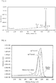
FIG. 3] FIG. 3 is a view of a spectrum obtained by measuring the upper surface of the electrode of Example 1 with X-ray photoelectron spectroscopy (a wide scan analysis). - [
FIG. 4] FIG. 4 is a view of the spectrum obtained by measuring the upper surface of the electrode of Example 1 with X-ray photoelectron spectroscopy (a narrow scan analysis). - With reference to
FIG. 1 , a carbon electrode that is an embodiment of the electrode of the present invention will be described. InFIG. 1 , the upper-lower direction of the paper sheet of the drawing is the upper-lower direction (the thickness direction, and the first direction). The upper side of the paper sheet is the upper side (the one side in the thickness direction, the one side in the first direction). The lower side of the paper sheet is the lower side (the other side in the thickness direction, the other side in the first direction). Meanwhile, the left-right direction and depth direction of the paper sheet are surface directions orthogonal to the upper-lower direction. Specifically, the directions conform to the direction arrows in each drawing. - A
carbon electrode 1 has a film shape (including a sheet shape) with a predetermined thickness, extends in a predetermined direction (surface direction) orthogonal to the thickness direction, and has a flat upper surface (a one-side surface in the thickness direction) and a flat lower surface (the other-side surface in the thickness direction). - Specifically, as illustrated in
FIG. 1 , thecarbon electrode 1 includes asubstrate 2, and aconductive carbon layer 3 disposed at an upper side (the one side in the thickness direction) of thesubstrate 2. In other words, thecarbon electrode 1 includes thesubstrate 2, and theconductive carbon layer 3 in the thickness direction. Preferably, thecarbon electrode 1 consists of thesubstrate 2 and theconductive carbon layer 3. Hereinafter, each of the layers will be described in detail. - The
substrate 2 is a substrate that supports theconductive carbon layer 3. Thesubstrate 2 is the lowest layer of thecarbon electrode 1, and disposed on an entire lower surface of theconductive carbon layer 3 so as to be in contact with a lower surface of theconductive carbon layer 3. - Examples of the
substrate 2 include an inorganic substrate and an organic substrate. - Examples of the inorganic substrate include a silicon substrate and a glass substrate.
- Examples of the organic substrate include polymer films. Examples of the material of the polymer film include polyester resins (such as polyethylene terephthalate, and polyethylene naphthalate), acetate resins, polyether sulfone resins, polycarbonate resins, polyamide resins, polyimide resins, polyolefin resins (such as polycycloolefin polymers), (meth)acrylic resins, polyvinyl chloride resins, polyvinylidene chloride resins, polystyrene resins, polyvinyl alcohol resins, polyarylate resins, and polyphenylenesulfide resins.
- The substrate has a thickness of, for example, 2 µm or more, preferably 20 µm or more and, for example, 1000 µm or less, preferably 500 µm or less.
- The
conductive carbon layer 3 is a layer that has electrode properties (such as a width of the potential window, and conductivity) and functions as an electrode. - The
conductive carbon layer 3 is formed of carbon having an sp2 bond and an sp3 bond. In other words, theconductive carbon layer 3 is a layer having a graphite structure and a diamond structure. In this manner, theconductive carbon layer 3 extends its potential window, and has good conductivity. Further, theconductive carbon layer 3 has excellent film-forming properties at a low temperature. - The ratio (sp3/sp3 + sp2) of the number of sp3 bonded atoms to the sum of the number of sp3 bonded atoms and the number of sp2 bonded atoms is, for example, 0.1 or more, preferably 0.2 or more, more preferably 0.25 or more, even more preferably 0.30 or more, particularly preferably 0.35 or more, particularly preferably 0.40 or more, particularly preferably 0.50 or more. Meanwhile, the ratio (sp3/sp3 + sp2) of the number of sp3 bonded atoms to the sum of the number of sp3 bonded atoms and the number of sp2 bonded atoms is, for example, 0.9 or less, preferably 0.5 or less.
- Where the ratio (sp3/sp3 + sp2) of the number of sp3 bonded atoms is the above-described lower limit or more, the potential window of the
carbon electrode 1 can be further extended for anodic direction when the concentration ratio (O/C) of oxygen to carbon is set in the range. In other words, where the ratio (sp3/sp3 + sp2) of the number of sp3 bonded atoms is less than the above-described lower limit, the potential window of thecarbon electrode 1 cannot further be extended for anodic direction even when the concentration ratio (O/C) of oxygen to carbon is set in the range. - To be more specific, there is a plurality of samples at the same ratio (sp3/sp3 + sp2) of the number of sp3 bonded atoms. The concentration ratio (O/C) of oxygen is 0.07 or more in a first sample, and the concentration ratio (O/C) of oxygen is less than 0.07 in a second sample. The potential window of the first sample for anodic direction is compared with the potential window of the second sample for anodic direction. As a result, the potential window of the first sample for anodic direction is wider than that of the second sample.
- On the other hand, when the ratio (sp3/sp3 + sp2) of the number of sp3 bonded atoms is the above-described upper limit or less, the conductivity of the
conductive carbon layer 3 decreases and the current signal becomes smaller. Thus, it is sometimes difficult to detect especially the signals in the low concentration region. - The above-described ratio can be calculated based on the peak intensity of the sp2 bond and the peak intensity of sp3 bond in the spectrum obtained by measuring the upper surface of the
conductive carbon layer 3 with X-ray photoelectron spectroscopy. The specific calculation will be described below in Examples. - On the upper surface of the
conductive carbon layer 3, the concentration ratio (O/C) of oxygen to carbon is, 0.07 or more, preferably 0.08 or more, more preferably 0.09 or more, particularly preferably 0.10 or more. When the above-described concentration ratio is the above-described lower limit or more, the potential window of thecarbon electrode 1 can be extended for anodic direction. Thus more compounds can be detected. - The upper limit of the above-described concentration ratio is not limited. However, to maintain the shape of the solid surface, the concentration ratio is, for example, 0.20 or less, preferably 0.15 or less.
- The above-described concentration ratio can be calculated based on the peak intensity of Cls and the peak intensity of O1s in the spectrum obtained by measuring the upper surface of the
conductive carbon layer 3 with X-ray photoelectron spectroscopy. The specific calculation will be described below in Examples. - The upper surface of the
conductive carbon layer 3 has a surface roughness Ra of, for example, 10 nm or less, preferably 5 nm or less, preferably 3 nm or less, preferably 1.0 nm or less, the most preferably 0.9 nm or less (or less than 1.0 nm). Meanwhile, the upper surface of theconductive carbon layer 3 has a surface roughness Ra of, for example, 0.01 nm or more, or 0.05 nm or more. - Where the surface roughness Ra is less than the above-described upper limit, the noise of the current can be suppressed when the
carbon electrode 1 is used as an electrode for an electrochemical measurement. Further, even when the concentration of the analytes to be measured is low, the response current can be detected without being buried in the background current. Thus, a measurement (electrochemical measurement) with good sensitivity can be carried out. - The surface roughness Ra of the upper surface of the
conductive carbon layer 3 can be measured by the observation of a 500 nm square of the upper surface of theconductive carbon layer 3 using an atom force microscope. - The upper surface of the
conductive carbon layer 3 has a surface resistance value of, for example, 1.0 × 10⁴Ω/□ or less, preferably 1.0 × 10³Ω/□ or less. The surface resistance value can be measured with a method with a four- probes method array in conformity with JIS K 7194. - The
conductive carbon layer 3 has a thickness of, for example, 5 nm or more, more preferably 10 nm or more and, for example, 200 nm or less, more preferably 100 nm or less. When the thickness of theconductive carbon layer 3 is the above-described lower limit or more, theconductive carbon layer 3 has excellent film-forming properties and thus can develop stable electrode properties. On the other hand, when the thickness of theconductive carbon layer 3 is the above-described upper limit or less, theconductive carbon layer 3 can be thinned and has excellent flexibility and thus is given good handleability. - The thickness of the
conductive carbon layer 3 can be calculated by the measurement of the X-ray reflectivity of theconductive carbon layer 3. The specific calculation will be described below in Examples. - The
conductive carbon layer 3 can contain another additive agent in addition to carbon. The conductive carbon layer can consist of a plurality of layers each having a different structure, composition, and additive agent concentration. Alternatively, theconductive carbon layer 3 can have a structure in which, for example, the structure, composition, and additive agent concentration gradually change (in gradations). - The
carbon electrode 1 is produced, for example, by a step of preparing thesubstrate 2, a step of providing thesubstrate 2 with a carbon thin film, and a step of an oxidation treatment of the carbon thin film. - First, a known or commercially
available substrate 2 is prepared. - Thereafter, for the adhesion of the
substrate 2 and theconductive carbon layer 3, as necessary, the upper surface of thesubstrate 2 can be subjected to a foundation process such as sputtering, a corona discharge, flames, ultraviolet light irradiation, electron beam irradiation, chemical conversion, or oxidation. Further, solvent cleaning or ultrasonic cleaning can be used to remove the dust and clean thesubstrate 2. - Next, the carbon thin film is provided on the upper surface of the
substrate 2. Preferably, a dry process is used to form theconductive carbon layer 3 on the upper surface of thesubstrate 2. - Examples of the dry process include a PVD method (physical vapor deposition method) and a CVD method (chemical vapor deposition method). Preferably, a PVD method is used.
- Examples of the PVD method include a sputtering technique, a vacuum deposition method, a laser deposition method, and an ion plating method (such as an arc deposition method). To reduce the hydrogen contained in the
conductive carbon layer 3 and surely form the film of theconductive carbon layer 3, preferably, a sputtering technique is used. - Examples of the sputtering technique include an unbalanced magnetron sputtering technique (UBM sputtering technique), a high-power pulsed sputtering technique, an electron cyclotron resonance sputtering technique, an RF sputtering technique, a DC sputtering technique (DC magnetron sputtering technique), a DC pulsed sputtering technique, an ion beam sputtering technique, and an ECR sputtering technique (electron cyclotron resonance sputtering technique).
- To easily form the film of the conductive carbon in a desired range of the ratio of sp3 bonds to sp2 bonds, to improve the film deposition rate and the adhesion to the substrate, to simplify the device structure, and to increase the ion irradiation, more preferably, a UBM sputtering technique is used.
- When a sputtering technique is used, the targeted material may be carbon (preferably, a sintered carbon). To adjust the film quality or stabilize the process, the targeted material may contain a known additive agent.
- Examples of the sputtering gas introduced into the film deposition chamber include inert gases such as Ar and Xe. To sputter the
conductive carbon layer 3, for example, an oxygen gas is not combined as a reactive gas. - The sputtering technique is carried out under vacuum. Specifically, to suppress the reduction in the sputtering rate and stabilize the electrical discharge, the atmospheric pressure at the sputtering is, for example, 1 Pa or less, preferably, 0.7 Pa or less.
- The film deposition temperature (the substrate temperature) is, for example, 200°C or less, preferably, 120°C or less and, for example, -40°C or more, preferably, 0°C or more.
- Further, to form the
conductive carbon layer 3 with a desired thickness, for example, the conditions for the targeted material or the sputtering can appropriately be set and the sputtering technique can be carried out several times. - In this manner, an intermediate including the
substrate 2 and the carbon thin film in the thickness direction is obtained. - Next, the carbon thin film of the intermediate is subjected to an oxidation treatment.
- As the oxidation treatment, any method that increases the oxygen atoms existing on the upper surface of the carbon thin film can be used. Examples of the oxidation treatment include a plasma treatment, and an electrochemical treatment. To simplify the production, preferably, an electrochemical treatment is used.
- In the electrochemical oxidation treatment, the intermediate is used as the working electrode for the electrochemical measurement. Then, a potential higher than the measurable potential limit (the maximum potential) is applied.
- For example, when the anodic potential limit, to the silver/silver chloride reference electrode is 1.9 V at the oxidation side in the potential window (measurement range)of the electrochemical measurement, a potential (for example, 2.3 V or higher) substantially exceeding 1.9 V is applied.
- The excessive potential is applied, for example, several times, specifically, twice or more, preferably, five times or more and, for example, 20 times or less.
- In this manner, the oxygen concentration on the upper surface of the carbon thin film increases, and the
conductive carbon layer 3 is formed. As a result, thecarbon electrode 1 including thesubstrate 2 and theconductive carbon layer 3 in the thickness direction is obtained. - The
carbon electrode 1 has a total thickness of, for example, 2 µm or more, preferably, 20 µm or more and, for example, 1000 µm or less, preferably 500 µm or less. - The
carbon electrode 1 can be used as various electrodes and, preferably, used as the electrode (preferably, the working electrode) for an electrochemical measurement. - When the
carbon electrode 1 is used as an electrode, an insulating layer patterned into a desired shape can be provided on the upper surface of the carbon electrode to adjust the exposed surface (electrode surface) of theconductive carbon layer 3. Alternatively, thecarbon electrode 1 or theconductive carbon layer 3 can entirely be pattered into a desired shape. Examples of the insulating layer include the polymer film in the above description of thesubstrate 2. - Examples of the electrochemical measurement method include techniques for measuring the potential difference such as a potential difference measurement method, and techniques for measuring the current such as an electrical conductivity measurement method, amperometry, voltammetry, and an alternating-current impedance method.
- In the electrochemical measurement system of the present invention, the
carbon electrode 1 is used as the working electrode. - Specifically, the electrochemical measurement system for a potential difference measurement technique includes the
carbon electrode 1, a reference electrode, a potentiometer that measures the electromotive force between the electrodes, and an electrolytic solution. Anelectrochemical measurement system 4 for a current measurement technique includes, as illustrated inFIG. 2 , thecarbon electrode 1, areference electrode 5, acounter electrode 6, apotentiostat 7 that controls the electrode potentials of the electrodes, an ammeter that measures the current flowing between thecarbon electrode 1 and the counter electrode 6 (the ammeter is not illustrated because being incorporated in the potentiostat), and an electrolytic solution 8 (seeFIG. 2 ). - Examples of the
reference electrode 5 include a silver/silver chloride electrode, a saturated calomel electrode, and a standard hydrogen electrode. Examples of the counter electrode6 include a platinum electrode, a gold electrode, and a nickel electrode. Examples of the electrolytic solution 8 include a phosphate buffered aqueous solution such as a sodium hydrogenphosphate aqueous solution, and a sulfuric acid aqueous solution. - When the threshold value of the current per unit area is 250 µA/cm2 in the
electrochemical measurement system 4, the anodic potential limit value of the potential window of, for example, the silver/silver chloride reference electrode is, for example, 1.8 V or more, preferably 1.9 V or more and, for example, 2.5 V or less. When the potential value is in the above-described range, compounds with a high potential such as uridylic acid, and inosine 5'-triphosphate can be detected. - Of the
carbon electrode 1 and theelectrochemical measurement system 4, theconductive carbon layer 3 has sp2 bonds and sp3 bonds, and the concentration ratio of oxygen to carbon is 0.07 or more on the upper surface (the one-side surface in the thickness direction) of theconductive carbon layer 3. Thus, the potential window extends for anodic direction. Hence, substances detected with high potential can be detected. For example, compounds such as uridylic acid, and inosine 5'-triphosphate can be detected. - Particularly, the ratio of the number of sp3 bonded atoms to the sum of the number of sp3 bonded atoms and the number of sp2 bonded atoms is, 0.35 or more. Thus, when the concentration ratio of oxygen is 0.07 or more, namely, high, the extension of the potential window can be increased.
- Especially, uridylic acid is included in RNA (such as uracil) as a partial structure. Thus, the
electrochemical measurement 1 can be used to quantify RNA. On the other hand, inosine 5'-triphosphate is a phosphate adduct of inosine and inosine is an intermediate to be formed into adenine or damaged adenine (deaminated adenine). Thus, for example, the metabolic pathway and damage of adenine can be evaluated. Especially, dephosphorylation is not required, and inosine can be quantified. In addition, these uridylic acid and inosine relate to umami ingredients in foods, and thus can be used to analyze the foods. - The mechanism for extending the potential window when the above-described concentration ratio is high is inferred as follows. However, the present invention is not limited to the following inference. It is known that, in comparison between a graphite structure (sp2 part) and a diamond structure (sp3 part), the sp3 bonded part has a wider potential window. Thus, it is presumed that, in the
conductive carbon layer 3 having an sp2 part and an sp3 part, oxygen is introduced to the sp2 part by the oxidation treatment, and the sp3 part on the surface of the conductive carbon layer is relatively increased, and thus the potential window is extended. These are presumed to cause the ratio of the number of sp3 bonded atoms to be 0.35 or higher. - The
carbon electrode 1 illustrated inFIG. 1 consists of thesubstrate 2 and theconductive carbon layer 3. However, for example, although not illustrated, one or 2 or more function layer(s) can be included between thesubstrate 2 and theconductive carbon layer 3 or at a lower side of thesubstrate 2. Examples of the function layer include a gas barrier layer, a conductive layer, an adhesive layer, a surface smoothing layer, and a hard coating layer. The function layer includes particles with a median size of 1.0 nm or less, or does not include a particle. In this manner, the upper surface of the function layer can be a flat surface. - The present invention will be more specifically described below with reference to Examples and Comparison Example. The present invention is not limited to any of the Examples and Comparison Example. The specific numeral values used in the description below, such as mixing ratios (contents), physical property values, and parameters can be replaced with the corresponding mixing ratios (contents), physical property values, parameters in the above-described "DESCRIPTION OF EMBODIMENTS", including the upper limit values (numeral values defined with "or less", and "less than") or the lower limit values (numeral values defined with "or more", and "more than").
- A silicon substrate with a thickness of 300 µm was prepared. Using a UBM sputtering technique, a carbon layer with a thickness of 35 nm was formed on an upper surface of the silicon substrate. For the conditions of the sputtering technique, a sintered carbon was used as the targeted material, the argon gas pressure was 0.6 Pa, the target power was 400 W, and the substrate temperature was 120°C or less. Meanwhile, a DC bias of 75 V was applied between the silicon substrate and the sintered carbon target (the targeted material). In this manner, a laminate including the substrate and the conductive carbon layer was produced.
- The laminate as the working electrode, a silver/silver chloride electrode as the reference electrode, and a platinum electrode as the counter electrode were connected to a potentiostat (manufactured by BAS Inc., the trade name of "CHI 802"), and thereby fabricating an electrochemical measurement system. As an electrolytic solution, 50 mmol/L of a phosphate buffer solution (a mixture solution of 50 mmol/L of an NaH2PO4 aqueous solution and 50 mmol/L of an Na2HPO4 aqueous solution, pH 7) was used.
- In the electrochemical measurement system, an applying potential of "0 V → 2.3 V → 0 V" was carried out 5 times to subject the surface of the laminate to an oxidation treatment, and thereafter the laminate was taken out. In this manner, a carbon electrode was produced.
- Except that the applying potential cycle was carried out 8 times, a carbon electrode was produced in the same manner as Example 1.
- Except that the applying potential cycle was carried out 15 times, a carbon electrode was produced in the same manner as Example 1.
- Except that the applying potential cycle was not carried out, a carbon electrode was produced in the same manner as Example 1.
- Except that an RF bias of 10 W was applied between the silicon substrate and the sintered carbon target (the targeted material) and the applying potential cycle was not carried out, a carbon electrode was produced in the same manner as Example 1.
- A carbon electrode was produced in the same manner as Example 1 except that the target power was changed from 400 W to 500 W, a DC bias was not applied between the silicon substrate and the sintered carbon target (the targeted material), and the applying potential cycle was not carried out. Thereafter, the surface of the electrode was subjected to UV irradiation by a UV/ozone device for 30 seconds while the distance between the UV lamp and the carbon electrode (the surface of the conductive carbon layer) was set to 5 mm, and thereby subjecting the conductive carbon layer to an oxidation treatment. Thereafter, the electrode was taken out. In this manner, the carbon electrode was produced.
- A carbon electrode was produced in the same manner as Example 1 except that a DC bias was not applied between the silicon substrate and the sintered carbon target (the targeted material), and the applying potential cycle was not carried out.
- Except that the applying potential cycle was not carried out and the surface was naturally oxidized, a carbon electrode was produced in the same manner as Comparative Example 4.
- Except that the target power was changed from 400 W to 300 W, the DC bias between the silicon substrate and the sintered carbon target (the targeted material) was changed from 75 V to 40 V, and the applying potential cycle was not carried out, a carbon electrode was produced in the same manner as Example 1.
- Except that the target power was changed from 500 W to 400 W, and the distance between the UV lamp and the carbon electrode (the surface of the conductive carbon layer) was set to 7 mm, a carbon electrode was produced in the same manner as Comparative Example 3.
- A carbon electrode was produced in the same manner as Example 1 except that the target power was changed from 400 W to 450 W, the DC bias between the silicon substrate and the sintered carbon target (the targeted material) was changed from 75 V to 50 V, and the applying potential cycle was not carried out.
- A carbon electrode was produced in the same manner as Example 1 except that the target power was changed from 400 W to 100 W, the DC bias between the silicon substrate and the sintered carbon target (the targeted material) was changed from 75 V to 100 V, and the applying potential cycle was not carried out.
- Except that the applying potential cycle was changed from "0 V → 2.3 V → 0 V" to "0 V → 2.2 V → 0 V", and the number of the times of the applying potential cycle was changed from 5 to 10, a carbon electrode was produced in the same manner as Comparative Example 8.
- Except that a PET substrate was used in place of the silicon substrate, a carbon electrode was produced in the same manner as Example 1.
- Except that a PET substrate was used in place of the silicon substrate and a hard coating layer with a thickness of 1.3 µm was disposed on the upper surface of the PET substrate, a laminate including the substrate, the hard coating layer, and the conductive carbon layer was produced in the same manner as Example 4. Subsequently, a carbon electrode was produced. The hard coating layer included particles with a median size of 15 nm.
- The arithmetic meant surface roughness Ra of the upper surface of each of the conductive carbon layers were measured in a range of 500 nm × 500 nm with an atomic force microscope (Digital Instruments, Inc., the trade name of "Nanoscope IV").
- Using X-ray reflectometry as the measurement principle, and a powder X ray diffractometer (manufactured by Rigaku Corporation, "RINT-2200"), under the following measurement conditions, the X-ray reflectivity was measured and the obtained measurement data was analyzed by an analytics software (manufactured by Rigaku Corporation, "GXRR3"), thereby calculating the film thickness. For the analysis, under the following <analysis conditions>, a two-layered model of an Si substrate and a two-layered model of the carbon film were used, and the targeted film thickness of the carbon film, the surface roughness of 0.5 nm, and the density of 1.95 g/cm3 were input as initial values, and thereafter Least Square fitting with the measured values was carried out, thereby analyzing the film thickness of the carbon film. The results are shown in Table 1 and Table 2.
-
- Measurement device: a powder X-ray diffractometer (manufactured by Rigaku Corporation, "RINT-2200")
- Light source: Cu-Kα rays (wavelength: 1,5418A), 40 kV, 40 mA
- Optical system: a parallel beam optical system
- Divergence slit: 0.05 mm
- Receiving slit: 0.05 mm
- Monochromatization-Paralellization: A multi-layered Goebel mirror was used.
- Measurement mode: θ/2θ scan mode
- Measurement range (2θ): 0.3-2.0°
-
- Analytics software: manufactured by Rigaku Corporation, "GXRR3"
- Analysis technique: Least squares fitting
- Analysis range: (2θ):2θ = 0.3-2.0°
- The upper surface of each of the conductive carbon layers was subjected to X-ray photoelectron spectroscopy under the following <Measurement conditions>. From the spectrum graph obtained from the measurement (see
FIG. 3 and FIG. 4 ), each peak area was obtained, thereby calculating the concentration ratio and the ratio of the number of carbon atoms. The concentration ratio (O/C) of oxygen to carbon is shown in Table 1 to Table 3. The ratio (sp3/sp3 + sp2) of the number of sp3 bonded carbon atoms to the sum of the number of sp2 bonded carbon atoms and the number of sp3 bonded carbon atoms is summarized in Table 1 to Table 3. -
- Measurement device: X-Ray Photoelectron Spectrometer (XPS) (manufactured by Shimadzu Corporation, the trade name of "AXIS Nova")
- X-ray source: AlKα (1486.6 eV) with a diameter 500 mm Rowland monochromator, 15 kV, 10 mA
- Photoelectron spectrometer: orbital radius 165 mm, a combination of a static double hemispherical analyzer/a spherical mirror analyzer
- Detector: a delay line detector (DLD) system
- Energy resolution: Ag3d5/2 photoelectron peak is the full width at half maximum of 0.48 eV or less.
- Charge neutralization: homogeneous low-energy electron irradiation
- An insulating tape having a hole with a
diameter 2 mm was adhered to the upper surface of each of the conductive carbon layers of Examples 4-7 and Comparative Examples 1-7, and the carbon electrode had an electrode area of 3.14 mm2. - The carbon electrode as the working electrode, the silver/silver chloride electrode as the reference electrode, the platinum electrode as the counter electrode were connected to the potentiostat (described above), thereby fabricating the electrochemical measurement system of each of Examples and Comparative Examples. As the electrolytic solution, 50 mmol/L of a sulfuric acid aqueous solution was used.
- A potential in a range between -2.4 V and +2.4 V was applied to the reference electrode of each of the electrochemical measurement systems at a scan rate of 0.1 V/s. The potential range in which the current value obtained in the potential application is between -500 µA/cm2 and + 500 µA/cm2 was defined as the range of the potential window. The anodic potential limit is summarized in Table 1 and Table 2.
- The electrode activities of the Ru complexes of Examples 1 to 3 were evaluated as ΔEp values. The results are summarized in Table 1. In the Table, the lower the ΔEp value is, the higher the the electrode activity is.
Table 1 Substrate Conductive carbon layer Potential window (V) [Anodic Potential limit] UMP Evaluation ITP Evaluation O/C ratio sp3 sp3+sp2 Film thickness (nm) Surface roughness Ra (nm) Example 1 Silicon 0.09 0.40 35 0.9 1.95 Good Good Example 2 0.09 0.40 5 0.8 1.94 Good Good Example 3 0.10 0.40 35 0.9 1.95 Good Good Comp. Ex. 1 0.03 0.40 35 0.9 1.73 Bad Bad Table 2 Substrate O/C ratio sp3 sp3+sp2 Potential window (V) [Anodic Potential limit] First sample / Second sample Comp. Ex. 2 Silicon 0.03 0.21 1.98 Second sample Comp. Ex. 3 Silicon 0.07 0.20 1.89 First sample Comp. Ex. 4 Silicon 0.03 0.23 2.02 Second sample Comp. Ex. 5 Silicon 0.08 0.22 2.02 First sample Comp. Ex. 6 Silicon 0.03 0.30 1.93 Second sample Comp. Ex. 7 Silicon 0.07 0.30 1.96 First sample Comp. Ex. 8 Silicon 0.03 0.41 2.06 Second sample Example 4 Silicon 0.08 0.40 2.32 First sample Comp. Ex. 9 Silicon 0.03 0.50 2.22 Second sample Example 5 Silicon 0.08 0.63 2.34 First sample Table 3 Substrate O/C ratio sp3 sp3+sp2 Ruthenium complex activity Δ Ep (V) Example 6 Silicon 0.08 0.48 79 Example 7 0.08 0.49 79 Example 8 0.10 0.53 85 - While the illustrative embodiments of the present invention are provided in the above description, such is for illustrative purpose only and it is not to be construed as limiting in any manner. Modification and variation of the present invention that will be obvious to those skilled in the art is to be covered by the following claims.
- The electrode is included, for example, in an electrochemical measurement system.
-
- 1
- carbon electrode
- 2
- substrate
- 3
- conductive carbon layer
- 4
- electrochemical measurement system
- 5
- reference electrode
- 6
- counter electrode
- 7
- potentiostat
- 8
- electrolytic solution
- Ra
- surface roughness of the upper surface of the conductive carbon layer
Claims (5)
- An electrode comprising:a substrate; anda conductive carbon layer disposed at one side in a thickness direction of the substrate and having an sp2 bond and an sp3 bond, whereina concentration ratio of oxygen to carbon is 0.07 or more on a one-side surface in the thickness direction of the conductive carbon layer, anda ratio of a number of sp3 bonded carbon atoms to a sum of a number of sp2 bonded carbon atoms and the number of sp3 bonded carbon atoms is 0.35 or more.
- The electrode according to Claim 1, wherein
the conductive carbon layer has a thickness of 5 nm or more and 200 nm or less. - The electrode according to Claim 1, wherein
the one-side surface in the thickness direction of the conductive carbon layer has a surface roughness Ra of 1.0 nm or less. - The electrode according to Claim 1, being an electrode for an electrochemical measurement.
- An electrochemical measurement system comprising the electrode according to Claim 4.
Applications Claiming Priority (3)
| Application Number | Priority Date | Filing Date | Title |
|---|---|---|---|
| JP2019036301 | 2019-02-28 | ||
| JP2020026156A JP6810330B2 (en) | 2019-02-28 | 2020-02-19 | Electrode and electrochemical measurement system |
| PCT/JP2020/007470 WO2020175471A1 (en) | 2019-02-28 | 2020-02-25 | Electrode and electrochemical measurement system |
Publications (2)
| Publication Number | Publication Date |
|---|---|
| EP3933394A1 true EP3933394A1 (en) | 2022-01-05 |
| EP3933394A4 EP3933394A4 (en) | 2022-11-09 |
Family
ID=72354022
Family Applications (1)
| Application Number | Title | Priority Date | Filing Date |
|---|---|---|---|
| EP20763408.0A Pending EP3933394A4 (en) | 2019-02-28 | 2020-02-25 | ELECTRODE FILM AND ELECTROCHEMICAL MEASUREMENT SYSTEM |
Country Status (5)
| Country | Link |
|---|---|
| EP (1) | EP3933394A4 (en) |
| JP (1) | JP6810330B2 (en) |
| KR (1) | KR20210129069A (en) |
| CN (1) | CN113474644B (en) |
| TW (1) | TWI821534B (en) |
Cited By (1)
| Publication number | Priority date | Publication date | Assignee | Title |
|---|---|---|---|---|
| EP4317958A4 (en) * | 2021-03-23 | 2025-03-26 | Nitto Denko Corporation | Electrode |
Families Citing this family (8)
| Publication number | Priority date | Publication date | Assignee | Title |
|---|---|---|---|---|
| WO2022202941A1 (en) * | 2021-03-23 | 2022-09-29 | 日東電工株式会社 | Electrode, and method for producing same |
| CN116997673A (en) * | 2021-03-23 | 2023-11-03 | 日东电工株式会社 | Electrode and manufacturing method |
| JPWO2022210176A1 (en) * | 2021-03-31 | 2022-10-06 | ||
| JP7277529B2 (en) * | 2021-09-14 | 2023-05-19 | 住友化学株式会社 | electrochemical sensor |
| US20250012753A1 (en) * | 2021-09-30 | 2025-01-09 | Nitto Denko Corporation | Electrode |
| JP7293413B1 (en) | 2022-01-26 | 2023-06-19 | 住友化学株式会社 | LAMINATED STRUCTURE FOR ELECTRODE AND METHOD FOR MANUFACTURING LAMINATED STRUCTURE FOR ELECTRODE |
| JP7821652B2 (en) * | 2022-03-24 | 2026-02-27 | 住友化学株式会社 | Electrode chip and electronic devices |
| WO2024232206A1 (en) * | 2023-05-11 | 2024-11-14 | 株式会社村田製作所 | Electrode and electrochemical measurement system |
Family Cites Families (7)
| Publication number | Priority date | Publication date | Assignee | Title |
|---|---|---|---|---|
| JP2005351677A (en) * | 2004-06-09 | 2005-12-22 | Matsushita Electric Ind Co Ltd | Electrodes and equipment for electrochemical testing and analysis |
| JP4513093B2 (en) * | 2004-09-24 | 2010-07-28 | 独立行政法人産業技術総合研究所 | Carbon electrode for electrochemical measurement and manufacturing method thereof |
| WO2010004690A1 (en) * | 2008-07-09 | 2010-01-14 | 日本電気株式会社 | Carbon electrode, electrochemical sensor, and carbon electrode manufacturing method |
| JP2013200260A (en) * | 2012-03-26 | 2013-10-03 | National Institute Of Advanced Industrial & Technology | Carbon electrode for electrochemical measurement and manufacturing method of the same |
| CN104280435A (en) * | 2014-09-28 | 2015-01-14 | 上海应用技术学院 | Graphene-modified glassy carbon electrode and preparation method and application of graphene-modified glassy carbon electrode |
| JP2018155728A (en) * | 2017-03-15 | 2018-10-04 | 学校法人東京理科大学 | Conductive diamond-like carbon microelectrode |
| JP6779820B2 (en) * | 2017-03-24 | 2020-11-04 | 株式会社東芝 | Electrodes, rechargeable batteries, battery packs and vehicles |
-
2020
- 2020-02-19 JP JP2020026156A patent/JP6810330B2/en active Active
- 2020-02-25 CN CN202080016483.8A patent/CN113474644B/en active Active
- 2020-02-25 KR KR1020217026829A patent/KR20210129069A/en not_active Ceased
- 2020-02-25 EP EP20763408.0A patent/EP3933394A4/en active Pending
- 2020-02-27 TW TW109106591A patent/TWI821534B/en active
Cited By (1)
| Publication number | Priority date | Publication date | Assignee | Title |
|---|---|---|---|---|
| EP4317958A4 (en) * | 2021-03-23 | 2025-03-26 | Nitto Denko Corporation | Electrode |
Also Published As
| Publication number | Publication date |
|---|---|
| JP6810330B2 (en) | 2021-01-06 |
| KR20210129069A (en) | 2021-10-27 |
| JP2020144116A (en) | 2020-09-10 |
| EP3933394A4 (en) | 2022-11-09 |
| TW202037911A (en) | 2020-10-16 |
| CN113474644A (en) | 2021-10-01 |
| CN113474644B (en) | 2024-04-12 |
| TWI821534B (en) | 2023-11-11 |
Similar Documents
| Publication | Publication Date | Title |
|---|---|---|
| TWI821534B (en) | Electrodes and electrochemical measurement systems | |
| EP3951375A1 (en) | Electrode and electrochemical measurement system | |
| EP3726207B1 (en) | Electrode film and electrochemical measurement system | |
| Pisonero et al. | Glow-discharge spectrometry for direct analysis of thin and ultra-thin solid films | |
| EP4130728A1 (en) | Electrode | |
| Protopopova et al. | Ultrathin undoped tetrahedral amorphous carbon films: thickness dependence of the electronic structure and implications for their electrochemical behaviour | |
| EP4650766A2 (en) | Electrode film and electrochemical measurement system | |
| US12159998B2 (en) | Electrode and electrochemical measurement system | |
| Shoja et al. | Microfabrication atomic layer deposited Pt NPs/TiN thin film on silicon as a nanostructure signal Transducer: Electrochemical characterization toward neurotransmitter sensing | |
| EP4224157A1 (en) | Electrode | |
| Jiwanti et al. | Modified Boron-Doped Diamond Electrodes for Sensors and Electroanalysis | |
| Svanberg‐Larsson et al. | A Comparison of Explicitly‐terminated Diamond Electrodes Decorated with Gold Nanoparticles | |
| TW202242911A (en) | electrode | |
| Bubert et al. | X‐Ray Photoelectron Spectroscopy (XPS) | |
| EP4624914A1 (en) | Electrode and electrochemical measurement system | |
| EP4597092A1 (en) | Electrode, and electrochemical measuring system | |
| EP4317521A1 (en) | Electrode, and method for producing same | |
| EP4597093A1 (en) | Electrode and electrochemical measurement system | |
| Guerreiro | LOW TOTAL ELECTRON YIELD N-DOPED GRAPHENE COATINGS PRODUCED BY ELECTROPHORETIC DEPOSITION | |
| Ito et al. | Electrochemical response and surface morphology of metal nanoparticles by pulsed laser deposition | |
| Corentin | ULB Faculty of Sciences Master in Chemistry | |
| Nunney | AVS2016 Session AS-TuP: Applied Surface Science Division Poster Session |
Legal Events
| Date | Code | Title | Description |
|---|---|---|---|
| STAA | Information on the status of an ep patent application or granted ep patent |
Free format text: STATUS: THE INTERNATIONAL PUBLICATION HAS BEEN MADE |
|
| PUAI | Public reference made under article 153(3) epc to a published international application that has entered the european phase |
Free format text: ORIGINAL CODE: 0009012 |
|
| STAA | Information on the status of an ep patent application or granted ep patent |
Free format text: STATUS: REQUEST FOR EXAMINATION WAS MADE |
|
| 17P | Request for examination filed |
Effective date: 20210826 |
|
| AK | Designated contracting states |
Kind code of ref document: A1 Designated state(s): AL AT BE BG CH CY CZ DE DK EE ES FI FR GB GR HR HU IE IS IT LI LT LU LV MC MK MT NL NO PL PT RO RS SE SI SK SM TR |
|
| DAV | Request for validation of the european patent (deleted) | ||
| DAX | Request for extension of the european patent (deleted) | ||
| A4 | Supplementary search report drawn up and despatched |
Effective date: 20221011 |
|
| RIC1 | Information provided on ipc code assigned before grant |
Ipc: C23C 14/58 20060101ALI20221005BHEP Ipc: C23C 14/06 20060101ALI20221005BHEP Ipc: G01N 27/30 20060101AFI20221005BHEP |
|
| STAA | Information on the status of an ep patent application or granted ep patent |
Free format text: STATUS: EXAMINATION IS IN PROGRESS |
|
| 17Q | First examination report despatched |
Effective date: 20241008 |
|
| GRAP | Despatch of communication of intention to grant a patent |
Free format text: ORIGINAL CODE: EPIDOSNIGR1 |
|
| STAA | Information on the status of an ep patent application or granted ep patent |
Free format text: STATUS: GRANT OF PATENT IS INTENDED |
|
| INTG | Intention to grant announced |
Effective date: 20260114 |
|
| GRAS | Grant fee paid |
Free format text: ORIGINAL CODE: EPIDOSNIGR3 |
|
| GRAA | (expected) grant |
Free format text: ORIGINAL CODE: 0009210 |
|
| STAA | Information on the status of an ep patent application or granted ep patent |
Free format text: STATUS: THE PATENT HAS BEEN GRANTED |