EP3932029B1 - Recuperation de phase d'horloge par usage des componsantes spectrales interieues - Google Patents
Recuperation de phase d'horloge par usage des componsantes spectrales interieues Download PDFInfo
- Publication number
- EP3932029B1 EP3932029B1 EP20789682.0A EP20789682A EP3932029B1 EP 3932029 B1 EP3932029 B1 EP 3932029B1 EP 20789682 A EP20789682 A EP 20789682A EP 3932029 B1 EP3932029 B1 EP 3932029B1
- Authority
- EP
- European Patent Office
- Prior art keywords
- values
- frequency
- signal
- results
- examples
- Prior art date
- Legal status (The legal status is an assumption and is not a legal conclusion. Google has not performed a legal analysis and makes no representation as to the accuracy of the status listed.)
- Active
Links
- 238000001514 detection method Methods 0.000 title description 14
- 230000003595 spectral effect Effects 0.000 title description 5
- 230000003287 optical effect Effects 0.000 claims description 76
- 238000004891 communication Methods 0.000 claims description 65
- 238000000034 method Methods 0.000 claims description 42
- 230000001419 dependent effect Effects 0.000 claims description 13
- 238000012886 linear function Methods 0.000 claims description 11
- 239000013598 vector Substances 0.000 description 58
- 238000011084 recovery Methods 0.000 description 33
- 238000001228 spectrum Methods 0.000 description 26
- 238000012545 processing Methods 0.000 description 19
- 230000000875 corresponding effect Effects 0.000 description 18
- 230000006870 function Effects 0.000 description 16
- 230000010287 polarization Effects 0.000 description 16
- 238000005070 sampling Methods 0.000 description 15
- 238000004364 calculation method Methods 0.000 description 9
- 238000005516 engineering process Methods 0.000 description 9
- 238000005259 measurement Methods 0.000 description 8
- 230000015556 catabolic process Effects 0.000 description 6
- 238000006731 degradation reaction Methods 0.000 description 6
- 239000006185 dispersion Substances 0.000 description 6
- 230000008569 process Effects 0.000 description 5
- 230000005540 biological transmission Effects 0.000 description 4
- 230000000694 effects Effects 0.000 description 4
- 238000003780 insertion Methods 0.000 description 4
- 230000037431 insertion Effects 0.000 description 4
- 230000010363 phase shift Effects 0.000 description 4
- 230000007704 transition Effects 0.000 description 4
- 238000001914 filtration Methods 0.000 description 3
- 230000004044 response Effects 0.000 description 3
- 238000012549 training Methods 0.000 description 3
- 230000003466 anti-cipated effect Effects 0.000 description 2
- 230000001427 coherent effect Effects 0.000 description 2
- 230000007423 decrease Effects 0.000 description 2
- 230000007246 mechanism Effects 0.000 description 2
- 230000000737 periodic effect Effects 0.000 description 2
- 238000013459 approach Methods 0.000 description 1
- 238000005311 autocorrelation function Methods 0.000 description 1
- 239000000969 carrier Substances 0.000 description 1
- 230000002596 correlated effect Effects 0.000 description 1
- 230000003247 decreasing effect Effects 0.000 description 1
- 238000013507 mapping Methods 0.000 description 1
- 239000013307 optical fiber Substances 0.000 description 1
- 230000001151 other effect Effects 0.000 description 1
- 238000000059 patterning Methods 0.000 description 1
- 230000009467 reduction Effects 0.000 description 1
- 238000007493 shaping process Methods 0.000 description 1
- 239000007787 solid Substances 0.000 description 1
- 230000002269 spontaneous effect Effects 0.000 description 1
- 230000001360 synchronised effect Effects 0.000 description 1
Images


Classifications
-
- G—PHYSICS
- G06—COMPUTING; CALCULATING OR COUNTING
- G06F—ELECTRIC DIGITAL DATA PROCESSING
- G06F1/00—Details not covered by groups G06F3/00 - G06F13/00 and G06F21/00
- G06F1/04—Generating or distributing clock signals or signals derived directly therefrom
- G06F1/12—Synchronisation of different clock signals provided by a plurality of clock generators
-
- H—ELECTRICITY
- H04—ELECTRIC COMMUNICATION TECHNIQUE
- H04L—TRANSMISSION OF DIGITAL INFORMATION, e.g. TELEGRAPHIC COMMUNICATION
- H04L7/00—Arrangements for synchronising receiver with transmitter
- H04L7/04—Speed or phase control by synchronisation signals
- H04L7/041—Speed or phase control by synchronisation signals using special codes as synchronising signal
- H04L7/042—Detectors therefor, e.g. correlators, state machines
-
- H—ELECTRICITY
- H03—ELECTRONIC CIRCUITRY
- H03L—AUTOMATIC CONTROL, STARTING, SYNCHRONISATION OR STABILISATION OF GENERATORS OF ELECTRONIC OSCILLATIONS OR PULSES
- H03L7/00—Automatic control of frequency or phase; Synchronisation
- H03L7/06—Automatic control of frequency or phase; Synchronisation using a reference signal applied to a frequency- or phase-locked loop
- H03L7/08—Details of the phase-locked loop
- H03L7/085—Details of the phase-locked loop concerning mainly the frequency- or phase-detection arrangement including the filtering or amplification of its output signal
- H03L7/087—Details of the phase-locked loop concerning mainly the frequency- or phase-detection arrangement including the filtering or amplification of its output signal using at least two phase detectors or a frequency and phase detector in the loop
-
- H—ELECTRICITY
- H04—ELECTRIC COMMUNICATION TECHNIQUE
- H04B—TRANSMISSION
- H04B10/00—Transmission systems employing electromagnetic waves other than radio-waves, e.g. infrared, visible or ultraviolet light, or employing corpuscular radiation, e.g. quantum communication
- H04B10/60—Receivers
- H04B10/66—Non-coherent receivers, e.g. using direct detection
- H04B10/69—Electrical arrangements in the receiver
- H04B10/695—Arrangements for optimizing the decision element in the receiver, e.g. by using automatic threshold control
-
- H—ELECTRICITY
- H04—ELECTRIC COMMUNICATION TECHNIQUE
- H04B—TRANSMISSION
- H04B10/00—Transmission systems employing electromagnetic waves other than radio-waves, e.g. infrared, visible or ultraviolet light, or employing corpuscular radiation, e.g. quantum communication
- H04B10/60—Receivers
- H04B10/66—Non-coherent receivers, e.g. using direct detection
- H04B10/69—Electrical arrangements in the receiver
- H04B10/697—Arrangements for reducing noise and distortion
-
- H—ELECTRICITY
- H04—ELECTRIC COMMUNICATION TECHNIQUE
- H04L—TRANSMISSION OF DIGITAL INFORMATION, e.g. TELEGRAPHIC COMMUNICATION
- H04L27/00—Modulated-carrier systems
- H04L27/26—Systems using multi-frequency codes
- H04L27/2601—Multicarrier modulation systems
- H04L27/2647—Arrangements specific to the receiver only
- H04L27/2655—Synchronisation arrangements
- H04L27/2662—Symbol synchronisation
- H04L27/2663—Coarse synchronisation, e.g. by correlation
-
- H—ELECTRICITY
- H04—ELECTRIC COMMUNICATION TECHNIQUE
- H04L—TRANSMISSION OF DIGITAL INFORMATION, e.g. TELEGRAPHIC COMMUNICATION
- H04L7/00—Arrangements for synchronising receiver with transmitter
- H04L7/0079—Receiver details
- H04L7/0087—Preprocessing of received signal for synchronisation, e.g. by code conversion, pulse generation or edge detection
-
- H—ELECTRICITY
- H04—ELECTRIC COMMUNICATION TECHNIQUE
- H04L—TRANSMISSION OF DIGITAL INFORMATION, e.g. TELEGRAPHIC COMMUNICATION
- H04L7/00—Arrangements for synchronising receiver with transmitter
- H04L7/0079—Receiver details
- H04L7/0083—Receiver details taking measures against momentary loss of synchronisation, e.g. inhibiting the synchronisation, using idle words or using redundant clocks
Definitions
- This document relates to the technical field of optical communications.
- an optical transmitter may transmit an optical signal over a communication channel to an optical receiver, where the signal is representative of digital information in the form of symbols or bits.
- the receiver may process the signal received over the communication channel to recover estimates of the symbols or bits.
- Various components of the optical communication network may contribute to signal degradation, such that the signal received at the receiver comprises a degraded version of the signal that was generated at the transmitter. Degradation or distortion may be caused by chromatic dispersion (CD), polarization mode dispersion (PMD), polarization dependent loss (PDL), and amplified spontaneous emission (ASE).
- CD chromatic dispersion
- PMD polarization mode dispersion
- PDL polarization dependent loss
- ASE amplified spontaneous emission
- the signal generated at the transmitter may be representative of a stream of symbols to be transmitted at a regular cadence according to times set by a symbol clock, where the frequency of the symbol clock is referred to as the symbol frequency or symbol rate or baud rate.
- estimates of the symbols may be recovered by sampling the received signal at times set by a sample clock, where the frequency of the sample clock is referred to as the sample frequency or sample rate.
- the accuracy of the symbol estimates depends on the precise timing of the samples in relation to the timing of the symbols in the received signal. Clock phase noise may result in jitter on the sample times relative to the symbol times, which in turn may reduce accuracy of the symbol estimates.
- the ability to achieve optimum sample timing at the receiver involves on a process referred to as clock recovery or timing recovery.
- US 2013/0039665 to Hauske describes a clock phase recovery apparatus configured to estimate clock signals based on an input signal.
- US 2012/0177156 to Hauske et al. describes a clock recovery apparatus configured to recover clock information from an input signal.
- a method is performed according to claim 1.
- the circuitry is also configured to implement the calculations performed as part of the method.
- the estimate of phase offset is calculated as a function of two or more results, that is, P ⁇ 2.
- the function is a non-linear function.
- the second sequence of values is identical to the first predefined sequence of values.
- each one of the P results is calculated by cross-correlating the first predefined sequence of values with a different portion of the representation.
- the estimate of the phase offset is calculated by multiplying one of the P results by the complex conjugate of another one of the P results.
- a complex value is calculated based on the P results, and the estimate of the phase offset is calculated from an angle of the complex value.
- a complex value is calculated based on the P results, and the estimate of the phase offset is calculated from an imaginary part of the complex value.
- calculating the P results comprises applying a frequency-dependent weight to the representation.
- the P results are calculated in the frequency domain.
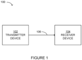
- FIG. 1 illustrates an example communication network 100, in accordance with some examples of the technology disclosed herein.
- the communication network 100 may comprise at least one transmitter device 102 and at least one receiver device 104, where the transmitter device 102 is capable of transmitting signals over a communication channel, such as a communication channel 106, and where the receiver device 104 is capable of receiving signals over a communication channel, such as the communication channel 106.
- the transmitter device 102 is also capable of receiving signals.
- the receiver device 104 is also capable of transmitting signals.
- the transceiver may comprise a modem.
- the communication network 100 may comprise additional elements not illustrated in FIG. 1 .
- the communication network 100 may comprise one or more additional transmitter devices, one or more additional receiver devices, one or more controller devices, and one or more other devices or elements involved in the communication of signals in the communication network 100.
- the signals that are transmitted and received in the communication network 100 may comprise any combination of electrical signals, optical signals, and wireless signals.
- the transmitter device 102 may comprise a first optical transceiver
- the receiver device 104 may comprise a second optical transceiver
- the communication channel 106 may comprise an optical communication channel.
- one or both of the first optical transceiver and the second optical transceiver may comprise a coherent modem.
- Each optical communication channel in the communication network 100 may include one or more links, where each link may comprise one or more spans, and each span may comprise a length of optical fiber and one or more optical amplifiers.
- the communication network 100 may comprise additional optical elements not illustrated in FIG. 1 , such as wavelength selective switches, optical multiplexers, optical de-multiplexers, optical filters, and the like.
- Frequency division multiplexing may be used to digitally divide up the modulated optical spectrum into a plurality of subcarriers, each with a different center frequency, such that each subcarrier may be used to transmit a signal that is representative of a different stream of symbols. In this manner, a plurality of symbol streams may be simultaneously communicated, in parallel, over the optical communication channel 106.
- FDM is possible when the frequencies of the subcarriers are sufficiently separated that the bandwidths of the signals do not significantly overlap.
- Each different subcarrier corresponds to a different FDM sub-band, also referred to as a FDM channel.
- FDM sub-band also referred to as a FDM channel.
- the use of Nyquist FDM sub-bands within one optical signal was described by Du et al. in "Optimizing the subcarrier granularity of coherent optical communications systems", Optics Express, Vol. 19, No. 9, pp. 8079-8084 (2011 ). It is also known to use a comb of optical tones that are precisely frequency locked as another way to achieve FDM within one optical signal.
- Wavelength division multiplexing may be used to transmit a plurality of data streams in parallel, over a respectively plurality of carriers, where each carrier is generated by a different laser.
- a signal received at the receiver device 104 may comprise a degraded version of a signal transmitted by the transmitter device 102.
- the signal transmitted by the transmitter device 102 may be degraded by optical amplifier noise, optical nonlinearity, polarization-dependent loss or gain (PDL or PDG), polarization mode dispersion (PMD), frequency-dependent loss, and other effects.
- the degree of signal degradation may be characterized by signal-to-noise ratio (SNR), or alternatively by noise-to-signal ratio (NSR).
- SNR signal-to-noise ratio
- NSR noise-to-signal ratio
- the signals transmitted in the communication network 100 may be representative of digital information in the form of symbols or bits.
- the signal generated at the transmitter device 102 may be representative of a stream of symbols to be transmitted at times set by a transmitter symbol clock, where the frequency of the transmitter symbol clock is set to be, for example, a certain ratio or fraction of a transmitter sampling frequency which may be set by a voltage controlled oscillator (VCO) and associated clocking circuits at the transmitter device 102.
- the frequency of the symbol clock at the transmitter device 102 may be referred to as the transmitter symbol frequency or symbol rate or baud rate.
- estimates of the symbols may be recovered by sampling the received signal at times set by a receiver sample clock, where the frequency of the receiver sample clock may be set by a VCO at the receiver device 104.
- the frequency of the sample clock at the receiver device 104 may be referred to as the receiver sample frequency or sample rate.
- the receiver sample rate may be selected to satisfy the Nyquist criterion for the highest anticipated transmitter symbol rate. For example, if the transmitter symbol rate is expected to be 10 GBaud, then the receiver sample rate may be set to 20 GHz.
- U.S. Pat. No. 7,701,842 to Roberts et al. describes using a fractional sample rate that is less than double the symbol rate.
- a symbol clock at the receiver device 104 may be set to be a certain ratio or fraction of the receiver sample rate and, after initial processing, the information stream may be resampled to a receiver symbol rate that is equal to the transmitter symbol rate.
- samples is generally used to refer to samples taken at the receiver symbol rate, or at some oversampling rate, depending upon the context.
- the accuracy of the symbol estimates depends on the precise timing of the samples in relation to the timing of the symbols in the received signal. For example, symbol sample points that are closer to transitions between different signals that are representative of adjacent symbols may provide noisier symbol estimates than symbol sample points that are centered between the transitions.
- the relationship between the symbol timing and the sample timing is constantly changing.
- the VCO at the transmitter device 102 may introduce phase noise and frequency deviations, such that a given symbol in the symbol stream may be transmitted at a time that is offset from the expected time defined by the symbol rate.
- the VCO at the receiver device 104 may also introduce phase noise and frequency errors, such that a given sample time may be offset from the desired sample time defined by the receiver symbol arrival times.
- Optimum sample timing at a receiver device may be achieved using a process known as clock recovery or timing recovery.
- clock recovery is implemented based on the measurements output by a clock phase detector.
- FIG. 2 illustrates an example transmitter device 200, in accordance with some examples of the technology disclosed herein.
- the transmitter device 200 is an example of the transmitter device 102.
- the transmitter device 200 is configured to transmit an optical signal 204 which is representative of information bits (also referred to as client bits) 202.
- the optical transmitter 200 employs polarization-division multiplexing (PDM).
- PDM polarization-division multiplexing
- generation of the optical signal 204 may involve alternative techniques, such as single polarization modulation, modulation of an unpolarized carrier, mode-division multiplexing, spatial-division multiplexing, Stokes-space modulation, polarization balanced modulation, and the like.
- a laser 214 is configured to generate a continuous wave (CW) optical carrier 212.
- a polarizing beam splitter 206 is configured to split the CW optical carrier 212 into polarized components 208 that are modulated by electrical-to-optical (E/O) modulators 218 to produce modulated polarized optical signals 216 that are combined by a beam combiner 210, thus yielding the optical signal 204.
- E/O electrical-to-optical
- the locations of the polarizing beam splitter 206 and the beam combiner 210 may be reversed.
- the polarizing beam splitter 206 and the beam combiner 210 may be replaced with simple power splitters and combiners. Together, elements such as the E/O modulators 218, the laser 214, the beam splitter 206, and the beam combiner 210 may form a communication interface configured to transmit optical signals to other devices in a communication network.
- the transmitter device 200 may comprise an application specific integrated circuit (ASIC) 222.
- ASIC application specific integrated circuit
- the ASIC 222 may be configured to apply FEC encoding 250 to the client bits 202 to generate FEC-encoded bits 248.
- the FEC-encoded bits 248 may be mapped to one or more streams of data symbols 244 according to a mapping 246.
- the symbols 244 may comprise a plurality of parallel streams of symbols where each stream corresponds to a different FDM subcarrier.
- the ASIC 222 may be configured to apply processing 232 to the one or more streams of symbols 244.
- the processing 232 may comprise digital up-sampling of the symbols 244.
- the processing 232 may further comprise operations that are subsequently applied to the sampled waveform, either in the time domain or the frequency domain. Such operations may include pulse shaping, FDM subcarrier multiplexing, chromatic dispersion precompensation, and distortion precompensation.
- the processing 232 may include the application of one or more filters, which may involve the application of one or more Fast Fourier Transforms (FFTs) and one or more corresponding inverse FFTs (IFFTs).
- FFTs Fast Fourier Transforms
- IFFTs corresponding inverse FFTs
- the processing 232 may further include the insertion of known symbols into the one or more streams of data symbols 244.
- known symbols For example, Huawei Technologies Co., Ltd. "FlexO-x-DTPC frame consideration," Standards Study Group 15, Geneva 25 Feb - 1 March 2019 describes the insertion of training symbols and pilot symbols for training receiver equalization and tracking carrier phase.
- digital drive signals 226, which comprise an electrical representation of the optical spectrum that is to be used in the transmission of the optical signal 204.
- the digital drive signals 226 may comprise four signals corresponding to the I and Q components of the X polarization and the I and Q components of the Y polarization.
- the transmitter device 200 comprises a plurality of digital-to-analog converters (DACs) 224 which may be used to convert the digital drive signals 226 into respective analog drive signals 220.
- the DACs 224 may be controlled by a signal 228 received from a VCO 230.
- the analog drive signals 220 are used to drive the E/O modulators 218, which ultimately results in the optical signal 204.
- the optical signal 204 is representative of the stream of symbols 244 (and any additional symbols inserted as a result of the processing 232).
- the symbol rate is dependent on the signal 228 generated by the VCO 230.
- imperfections in the operation of the VCO 230 may result in small variations in the symbol phase away from a constant symbol rate. These variations are one source of the jitter to be corrected by clock recovery at a receiver device.
- the DACs 224 or portions thereof may be separate from the ASIC 222.
- the transmitter device 200 may comprise additional components that are not described in this document.
- FIG. 3 illustrates an example receiver device 300, in accordance with some examples of the technology disclosed herein.
- the receiver device 300 is an example of the receiver device 104.
- the receiver device 300 is configured to recover corrected client bits 302 from a received optical signal 304.
- the received optical signal 304 may comprise a degraded version of an optical signal generated by a transmitter device, such as the transmitter device 102 or 200.
- a polarizing beam splitter 306 is configured to split the received optical signal 304 into polarized components 308.
- the polarized components 308 may comprise orthogonally polarized components corresponding to an X polarization and a Y polarization.
- An optical hybrid 310 is configured to process the components 308 with respect to an optical signal 312 produced by a laser 314, thereby resulting in optical signals 316.
- Photodetectors 318 are configured to convert the optical signals 316 output by the optical hybrid 310 to analog signals 320.
- the analog signals 320 may comprise four signals corresponding, respectively, to the dimensions XI , XQ , YI , YQ , where XI and XQ denote the in-phase and quadrature components of the X polarization, and YI and YQ denote the in-phase and quadrature components of the Y polarization.
- elements such as the beam splitter 306, the laser 314, the optical hybrid 310 and the photodetector 318 may form a communication interface configured to receive optical signals from other devices in a communication network.
- the receiver device 300 may comprise an ASIC 322.
- the ASIC 322 may comprise analog-to-digital converters (ADCs) 324 which are configured to sample the analog signals 320, and to generate respective digital signals 326.
- the ADCs 324 sample the analog signals 320 periodically at a sample rate that is based on a signal 328 received from a VCO 330. Similar to the VCO 230 at the transmitter device 200, imperfections in the operation of the VCO 330 at the receiver device 320 may result in small variations in the sample phase away from a constant sample rate. These variations are an additional source of jitter to be corrected by clock recovery.
- the ASIC 322 is configured to apply digital processing 332 to the digital signals 326.
- the processing 332 may comprise the application of one or more filters to the digital signals 326, which may involve the application of one or more FFTs and one or more corresponding IFFTs.
- the processing 332 may also include down-sampling, FDM subcarrier de-multiplexing, chromatic dispersion post-compensation, and distortion post-compensation.
- the processing 332 further comprises clock recovery 334.
- the clock recovery 334 may be implemented by circuitry which makes use of a clock phase detector 336.
- the clock phase detector 336 is configured to use the digital signals 326 to generate measurements of phase offset of the sample timing relative to the timing of the symbols represented by the analog signals 320.
- clock phase offset may be understood to refer to the phase offset of a clock which operates continuously (e.g., for minutes up to years) with respect to a signal stream, where the signal stream may carry on the order of gigabits to terabits per second across large distances (e.g., kilometers).
- the phase offset measurements output by the clock phase detector 336 may be used to achieve the clock recovery 334 in one or more ways.
- the clock recovery 334 may be implemented by sending a feedback signal 338 to the VCO 330 based on the phase offset measurements output by the clock phase detector 336.
- the feedback signal 338 may be generated by applying a low-pass filter to the phase offset measurement output by the clock phase detector 336.
- the feedback signal 338 may result in slight adjustments of the frequency of the VCO 330, which in turn will cause slight adjustments in the sample timing at the ADCs 324.
- This feedback technique for clock recovery is commonly known as a phase lock loop (PLL).
- the clock recovery 334 may be implemented by using the phase offset measurements output by the clock phase detector 336 to generate a phase shift in the signal 328 output by the VCO 330.
- clock phase shifter hardware (not shown) that is known in the art.
- the clock recovery 334 may be implemented by using the phase offset measurements output by the clock phase detector 336 to generate a phase shift in a downstream version of the digital signals 326.
- This mechanism for clock recovery would be implemented using data phase shifter hardware (not shown) that is known in the art, either in the time domain or in the frequency domain.
- the data phase shifter may be applied to a plurality of FDM sub-bands. Both the clock phase shifter and the data phase shifter may rely on a signal generated by applying a finite impulse response (FIR) filter or an infinite impulse response (IIR) filter to the phase offset measurement output by the clock phase detector 336.
- FIR finite impulse response
- IIR infinite impulse response
- processed digital signals 340 may undergo carrier recovery 342.
- the carrier recovery 342 may be used to recover symbol estimates 344, which may in turn undergo symbol-to-bit demapping 346 to recover bit estimates 348.
- the bit estimates 348 may further undergo FEC decoding 350 to recover the corrected client bits 302.
- the ADCs 324 or portions thereof may be separate from the ASIC 322.
- the receiver device 300 may comprise additional components that are not described in this document.
- an aim of the clock recovery 334 is to correct jitter caused by transmitter VCO 230 and receiver VCO 330.
- jitter may also arise from numerical noise or electrical noise in the PLL, or from noise or artifacts in the clock phase detector 336.
- the clock recovery 334 may address all of these sources of jitter for the purpose of achieving the optimum sample timing at the receiver device 300.
- the accuracy of the clock phase detector 336 may be reduced by various types of signal distortion or degradation, such as CD, PMD, PDL, and ASE. Optical filtering may also reduce the accuracy of the clock phase detector 336.
- U.S. Pat. No. 7,627,252 to Sun et al. describes a technique for clock recovery following dispersion compensation.
- U.S. Pat. No. 7,532,822 to Sun et al. describes a technique for clock recovery following compensation of polarization effects.
- U.S. Pat. No. 8,135,283 to Sun et al. describes a technique for clock recovery following compensation of inter-symbol interference (ISI) due to polarization effects.
- ISI inter-symbol interference
- a raised cosine filter to the signal in the frequency domain has the desirable effects of achieving zero ISI in the time domain and minimum noise bandwidth.
- a root-raised cosine filter at each device, also known as matched filters.
- the processing 232 applied at the transmitter device 200 may include a first raised-root cosine filter
- the processing 332 applied at the receiver device 300 may include a second raised-root cosine filter.
- the shape of the raised cosine achieved by the pair of matched filters is characterized by a roll-off factor ⁇ . As the value of the roll-off factor ⁇ approaches zero, the shape of the raised cosine becomes closer to a rectangle function in the frequency domain.
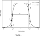
- FIG. 4 illustrates example frequency spectra of a received signal filtered using raised cosine filters having different roll-off factors, in accordance with some examples of the technology disclosed herein.
- the range of amplitude values, the range of frequency values, and the values of the roll-off factors are for illustrative purposes only and should not be considered necessarily limiting.
- the symbol rate is denoted by f s .
- a comparison of the two curves shows that decreasing the value of the roll-off factor ⁇ results in sharper roll-off regions and less energy extending beyond ⁇ f s /2.
- the method of clock phase detection described by Godard involves calculations which are performed on frequency components within the roll-off regions of the raised cosine spectrum.
- frequency components in one roll-off region are multiplied by the complex conjugate of frequency components in the other roll-off region and then summed. These counterpart frequency components are separated by the symbol rate f s .
- An example pair of counterpart frequency components, also referred to as a Godard pair is denoted by points A and B in FIG. 4 . It may be shown that the product of one component and the complex conjugate of another component contains clock phase information.
- the same operation may be applied to many different Godard pairs over a range of frequencies, and the results may be averaged to obtain an estimate of the clock phase offset.
- the roll-off factor ⁇ so as to limit the amount of signal excess bandwidth (i.e., bandwidth occupied beyond the symbol rate) as well as minimize the energy in the roll-off regions. Any unused portions of the spectrum beyond ⁇ f s /2 could be harvested for improved spectral efficiency. For example, sharper roll-off regions could allow for closer proximity between FDM sub-bands, or wavelength divisional multiplexing (WDM) bands, or both. Reducing the amount of energy in the roll-off regions may also avoid problems with optical filters cutting off the Godard band, which would result in clock failure.
- WDM wavelength divisional multiplexing
- the ability to reduce the value of the roll-off factor is limited by the fact that the Godard method is reliant on the signals in the roll-off regions.
- the products computed from the Godard pairs will become increasingly noisy as the frequency width over which the Godard method is applied decreases.
- clock phase detection using the Godard method may become less reliable, and may eventually result in clock failure.
- a sequence of symbols is often organized into frames, with F symbols per frame.
- the value of F is generally on the order of one thousand to one hundred thousand.
- U.S. Pat. No. 8,463,133 to Roberts describes using a correlation to periodic SYNC patterns to estimate probabilities of locations of such a frame. Finding frame is distinct from finding clock frequency and clock phase. In most systems with continuous streams of symbols, frame cannot be found until after the symbol clock frequency is stably tracked.
- a reference vector be defined which comprises a first predefined sequence of values.
- a receiver device is operable or configured to store the reference vector, for example, in a control processor or by defining the reference vector in circuitry of the receiver device.
- a transmitter device may be operable or configured to transmit a communications signal to the receiver device, wherein the communications signal conveys or is representative of a second predefined sequence of values.
- the second predefined sequence of values is related to the first predefined sequence of values. According to some examples, they could be partially or substantially correlated. According to some examples, they could be rotated in the available dimensions or scaled.
- the first sequence of values could have a different sampling rate or phase than the second sequence of values.
- the second predefined sequence of values may be identical to the first predefined sequence of values.
- the second predefined sequence of values may be transmitted at a rate which is related to a symbol rate of the communications signal.
- the rate of the values in the second predefined sequence may be substantially equal to the symbol rate, or may be related to the symbol rate by an integer ratio.
- the receiver device may be operable or configured to receive the communications signal via a communication interface and to extract a representation of the received communications.
- the receiver device is operable or configured to calculate P results from a cross-correlation of the first sequence of values with at least a portion of the representation, where P is a positive integer.
- the receiver device may further be operable or configured to calculate an estimate of a clock phase offset as a function of the P results.
- the function may be a linear function or a non-linear function. Examples of the function are provided in Equations 12, 13, 15, 16, 18, 19, and 20.
- the estimate of the clock phase offset may be used for clock recovery, for example, as described with respect to FIG. 3 .
- the values in the first sequence and the second sequence may comprise known values, which may represent or comprise known symbols.
- the first sequence of values and the second sequence of values may comprise a synchronization (SYNC) pattern.
- the values may be repeated at a constant interval, or may follow a known pattern such as a pseudo-random pattern that determines location in time-sequence and values.
- the values may produce a relatively white spectrum.
- the communications signal may comprise information-bearing symbols
- the transmitter device may be configured to insert the first sequence of values into the communications signal at time locations where there are no information-bearing symbols.
- the values in the first sequence may add or multiply or otherwise modify the stream of information-bearing symbols in the communications signal.
- the receiver device may be configured to extract the representation of the optical signal by converting the optical signal into an electrical analog signal, converting the analog signal into a digital signal by digitally sampling the analog signal at a sample rate, and generating a signal vector based on the digital signal, where the signal vector is the representation of the communications signal.
- the sample rate may be equal to or greater than the symbol rate.
- the predefined sequence of symbols would be represented by signal values S 1 , S 2 , S 3 , S 4 at positions p 1 , p 2 , p 3 , p 4 , respectively.
- the time-domain reference vector r [ n ] would be defined as S 1 , S 2 , S 3 , S 4 , 0, 0, 0.
- N L.
- a FFT operation may be applied to the time-domain reference vector r [ n ] to obtain a corresponding frequency-domain reference vector R [ n ], as provided by Equation 2:
- R n FFT r n
- the frequency-domain reference vector R [n] consists of N values.
- an up-sampling operation may be applied to the frequency-domain reference vector R [n] to obtain a corresponding up-sampled frequency-domain reference vector R ⁇ [ f ], as provided by Equation 3:
- the up-sampling operation may be implemented by copying a portion of one or both sides of the spectrum to the corresponding other side of the spectrum.
- the up-sampling ratio may be an integer fraction that is at least 1, and at most 2.
- R ⁇ [ f ] provided by Equation 3 represents a reference vector comprising a first predefined sequence of values.
- This reference vector may be stored at the receiver device.
- the reference vector may be stored in a control processor and loaded into a register.
- the reference vector may be defined in circuitry of the receiver device.
- the receiver device may extract a representation of the communications signal.
- the receiver device may calculate P results by cross-correlating the first predefined sequence of values with at least a portion of the representation, where P is a positive integer. To understand how these results may be used to estimate a clock phase offset at the receiver device, the anticipated properties of the representation extracted at the receiver device will be derived from the communications signal transmitted by the transmitter device.
- the communications signal generated at the transmitter device conveys a second predefined sequence of values which is related to the first predefined sequence of values.
- the second predefined sequence of values may be periodically inserted into client data symbols using the processing 232.
- the communications signal is assumed to be an optical signal.
- the examples involve a single carrier communications signal conveying a single sequence of values in a single polarization.
- the sequence or signal may span various dimensions, polarizations, wavelengths, or carrier frequencies.
- the optical signal may comprise K FDM sub-bands, where K ⁇ 1.
- the predefined sequence of known symbols may be periodically inserted into client data symbols, for example, by the processing 232.
- Each predefined sequence of known symbols may be inserted as a block of consecutive symbols, or alternatively, may be interspersed with the client data symbols.
- the predefined sequence of known symbols may have an auto-correlation function that is as close as possible to a Dirac delta function.
- a FFT operation may be applied to each time-domain signal vector x k [ m ] to obtain a corresponding frequency-domain signal vector X k [ m ], as provided by Equation 5:
- X k m FFT x k m
- the k th frequency-domain signal vector X k [ m ] consists of N values.
- an up-sampling operation may be applied to each frequency-domain signal vector X k [ m ] to obtain a corresponding up-sampled frequency-domain signal vector X ⁇ k [ r ], as provided by Equation 6:
- the up-sampled frequency-domain signal vectors X ⁇ k [ r ] may be concatenated to form a single larger up-sampled frequency-domain signal vector X ⁇ [ f ] .
- X ⁇ f : X ⁇ 1 r , X ⁇ 2 r , ... , X ⁇ K r
- f 1.. KN u .
- K 1, X ⁇ [ f ] simplifies to X ⁇ 1 [ r ].
- the transmitter device may convert the signal vector X ⁇ [ f ] into an optical signal which may be transmitted to the receiver device.
- the receiver device is expected to receive a degraded version of the optical signal that was transmitted by the transmitter device.
- the differences between the received signal vector ⁇ [ f ] and the original signal vector X ⁇ [ f ] may be modeled by assuming a specific frequency-dependent noise distribution, and also by assuming a specific value of clock phase offset for the values in a time-domain vector that corresponds to the frequency-domain vector ⁇ [ f ] .
- the amount of correlation between the reference vector R ⁇ [ f ] provided by Equation 3 and the signal vector ⁇ [ f ] provided in Equation 8 may be used to estimate the clock phase offset T, based on the relationship defined by Equation 9.
- R ⁇ *[ f ] denotes the complex conjugate of R ⁇ [ f ].
- Equation 11 is only used to calculate cross-correlation values for the outer FDM sub-bands, thereby resulting in two cross-correlation values, C 1 and C 4 , corresponding to the lowest frequency FDM sub-band and the highest frequency FDM sub-band, respectively.
- each different cross-correlation value is calculated from a signal vector corresponding to a different FDM sub-band.
- each different cross-correlation value is calculated from a signal vector corresponding to a different portion of a single FDM sub-band.
- the signal vectors ⁇ k [ r ] instead of the signal vectors ⁇ k [ r ] corresponding to K different FDM sub-bands, they could correspond to K different portions of a single FDM sub-band.
- a single FDM sub-band could be divided into four quarters, as defined by Equation 14:
- Y ⁇ f : Y ⁇ NHB r , Y ⁇ NLB r , Y ⁇ PLB r , Y ⁇ PHB r
- ⁇ NHB [ r ] denotes the negative high-band portion of spectrum
- ⁇ NLB [ r ] denotes the negative low-band portion of spectrum
- ⁇ PLB [ r ] denotes the positive low-band portion of spectrum
- ⁇ PHB [ r ] denotes the positive high-band portion of spectrum.
- Equation 11 would result in four cross-correlation values C PHB , C PLB , C NLB , C NHB .
- Equations 12 and 13, used in Examples 1 and 2 respectively, may be modified to apply to the cross-correlation values C PHB , C PLB , C NLB , C NHB , as shown by Equations 15 and 16, respectively:
- the clock phase offset is estimated as a non-linear function of P cross-correlation results, where P ⁇ 2.
- Estimates of clock phase offset are calculated based on cross-correlation values that are weighted by a frequency-dependent weighting, as will be described in the following examples.
- Equation 9 may be approximated by replacing the exponent function with the first two terms of a Taylor series, according to Equation 17: Y ⁇ f ⁇ X ⁇ f 1 + j 2 ⁇ f ⁇ + Z f
- Imag( ) denotes the imaginary part of a complex value
- ⁇ denotes a constant that is independent from signal, noise, and clock jitter.
- R ⁇ * [ f ] f acts as a template to be applied to the signal vector ⁇ [ f ], where the template is weighted by the frequency f .
- the frequency f By using a frequency-dependent weight, it may be possible to achieve lower noise in the phase estimate when the higher frequencies have less noise.
- each different value of the frequency f produces a distinct result from the cross-correlation, and the clock phase offset ⁇ 3 is calculated as a linear function of these results.
- ⁇ denotes a constant that is independent from signal, noise, and clock jitter.
- R ⁇ *[ f ] sin(2 ⁇ f ) acts as a template to be applied to the signal vector ⁇ [ f ], where the template includes the frequency-dependent weighting sin(2 ⁇ f ).
- each different value of the frequency f produces a distinct result from the cross-correlation, and the clock phase offset ⁇ 4 , is calculated as a function of these results.
- the clock phase offset is calculated as a function of P results, where P ⁇ 2.
- the clock phase offset may be calculated as a function of a single cross-correlation result.
- the estimate of clock phase offset, ⁇ 5 may be noisy due to noise and data patterning, and consequently may need to be filtered in the time domain, or in the frequency domain, or via the control loop.
- FIG. 5 illustrates an example method 500 for clock phase detection in accordance with some examples of the technology disclosed herein.
- the method 500 may be performed at a receiver device, such as the receiver device 104 or 300.
- a first sequence of values is stored at the receiver device.
- the frequency-domain reference vector R ⁇ [ f ] defined by Equation 3 may be stored in a control processor of the receiver device and loaded into a register, or may be defined by circuitry of the receiver device.
- the first sequence of values stored at 502 may be defined in the time domain rather than the frequency domain.
- the time-domain reference vector r [ n ] defined by Equation 1 may be stored in a memory of the receiver device.
- a communications signal is received at the receiver device.
- the communications signal comprises a degraded version of a communications signal generated by a transmitter device.
- the communications signal may comprise a degraded version of the optical signal 204 transmitted by the transmitter device 200, where the optical signal 204 is representative of a stream of symbols transmitted at a symbol rate set by the VCO 230.
- the communications signal received at 504 conveys a second sequence of values, where the second sequence of values is related to the first sequence of values stored at 502. For example, as described with respect to FIG. 2 , the second sequence of symbols may be periodically inserted into the one or more streams of symbols 244 using the processing 232.
- a representation of the communications signal received at 504 is calculated.
- the received optical signal 304 may be split into the polarized components 308 by the beam splitter 306, the optical hybrid 310 may process the polarized components 308 with respect to the optical signal 312 produced by the laser 314, and the resulting optical signals 316 output by the optical hybrid 310 may be converted to the analog signals 320.
- the ADCs 324 may sample the analog signals 320 at the sample rate set by the VCO 330 to generate the respective digital signals 326.
- the representation may be based on the digital signals 326. Calculation of the representation may include the application of a FFT to the digital signals 326.
- the representation may comprise the frequency-domain signal vector ⁇ [ f ] defined by any one of Equations 8, 10, and 14.
- the representation calculated at 506 may comprise a time-domain signal vector, rather than a frequency-domain signal vector.
- the frequency-domain signal vector ⁇ [ f ] may comprise an up-sampled signal, as the ADC sampling rate is generally higher than the symbol rate in order to accommodate for signal energy present in the Godard band. Down-sampling of the frequency-domain signal vector ⁇ [ f ] may performed after estimating clock phase offset, as described with respect to step 510.
- P results are calculated by cross-correlating the first sequence of values stored at 502 with at least a portion of the representation calculated at 506, where P is a positive integer value.
- P a positive integer value.
- P ⁇ 2.
- the cross-correlation may be performed in the frequency domain or the time domain.
- the cross-correlation may be performed digitally with high-speed hardware, performed more slowly with a processor, or may be implemented as analog circuits such as matched filtering.
- Full cross-correlation may be performed, or partial cross-correlation may be performed, such as only for certain frequency terms or time locations, or an approximation to a correlation.
- a plurality of cross-correlation results may be calculated, such as the four cross-correlation results C 1 , C 2 , C 3 , C 4 calculated in Example 1, or the two cross-correlation results C 1 and C 4 calculated in Example 2, where each different cross-correlation result is calculated by cross-correlating the first sequence of values with a different portion of the representation of the communications signal.
- Each different portion of the representation may comprise a different FDM sub-band, or a different portion of a single FDM sub-band.
- cross-correlation results C PHB , C PLB , C NLB , C NHB may be calculated from a positive high-band portion of spectrum, a positive low-band portion of spectrum, a negative low-band portion of spectrum, and a negative high-band portion of spectrum, respectively.
- the different portions of the spectrum may comprise partially overlapping frequencies or disjoint frequencies.
- cross-correlation results may be calculated, for example, as described with respect to Examples 3 and 4, by cross-correlating the first sequence of values with the entire representation of the communications signal, together with a frequency-dependent weighting.
- a plurality of cross-correlation result may be calculated by applying the reference vector R ⁇ [ f ] to the entire signal vector ⁇ [ f ] with a weighting f or with a weighting sin(2 ⁇ f ).
- the P cross-correlation results calculated at 508 may represent the cross-correlation between the first sequence of values and the entire frequency spectrum of the representation, or substantially the entire frequency spectrum of the representation, or only portions of the frequency spectrum of the representation.
- an estimate of a clock phase offset between the symbol rate and the sample rate is calculated as a function of the P cross-correlation results calculated at 508.
- the function may comprise a non-linear function.
- the non-linear function may comprise a conjugate multiplication operation applied to pairs of spectral results.
- the non-linear function may comprise other time-domain or frequency-domain non-linear operations on two or more results.
- an estimate of the clock phase offset may be calculated from the angle of a complex value, where the complex value is based, for example, on four cross-correlation results according to Equation 12 or Equation 15, or based on two cross-correlation results according to Equation 13 or Equation 16.
- the clock phase offset may be estimated from by applying a function substantially equivalent to a complex-conjugate multiply of a pair of sub-band correlations.
- an estimate of the clock phase offset may be calculated from the imaginary part of a complex value, where the complex value is based on frequency-weighted cross-correlation results, for example, as provided in Equation 18 or Equation 19.
- an estimate of the clock phase offset may be calculated as a function of a single cross-correlation value, for example, as provided in Equation 20.
- the estimate of the clock phase offset calculated at 510 may have a range of possible values, where the range may substantially span a unit interval (UI), or the time interval occupied by one symbol.
- UI unit interval
- the estimate of the clock phase offset calculated at 510 may be used for clock recovery, as described with respect to FIG. 3 .
- the clock phase offset may be used to adjust the frequency of the VCO 330 as part of a PLL.
- the clock phase offset may be used to generate a phase shift in the signal output by the VCO 330.
- the clock phase offset may be used to generate a phase shift of a downstream version of the digital signals.
- clock phase detection circuit In optical transmission systems carrying hundreds of gigabits per second, it may be desirable to have a clock phase detection circuit that does not add significant heat or size to the receiver device, nor add significant delay to the continuous stream of bits being transmitted. This may be achieved, for example, via an ASIC implementation of the frequency-domain version of the methods described herein, where FFT hardware is already required for other signal processing functions.
- the clock of the digital circuitry implementing the clock phase detection may operate at a small fraction of the symbol rate, such as 1/128 or 3/256, for example.
Landscapes
- Engineering & Computer Science (AREA)
- Computer Networks & Wireless Communication (AREA)
- Signal Processing (AREA)
- Physics & Mathematics (AREA)
- Theoretical Computer Science (AREA)
- Electromagnetism (AREA)
- General Engineering & Computer Science (AREA)
- General Physics & Mathematics (AREA)
- Optical Communication System (AREA)
- Synchronisation In Digital Transmission Systems (AREA)
Claims (11)
- Procédé (500) exécuté au niveau d'un appareil récepteur (104, 300), le procédé comprenant : le stockage (502) d'une première séquence de valeurs prédéfinie ;la réception (504) d'un signal de communication optique (304), dans lequel le signal de communication optique transporte une seconde séquence de valeurs, la seconde séquence de valeurs étant liée à la première séquence de valeurs prédéfinie ;la calcul (506) d'une représentation du signal de communication optique ;le calcul (508) de P résultats à partir d'une corrélation croisée de la première séquence de valeurs prédéfinie avec au moins une partie de la représentation, dans lequel P est un entier positif ; etle calcul (510) d'une estimation d'un décalage de phase d'une horloge de symbole continue en fonction des P résultats,dans lequel le calcul des P résultats comprend l'application d'un poids dépendant de la fréquence à la représentation.
- Procédé selon la revendication 1, dans lequel la fonction est une fonction non linéaire.
- Procédé selon la revendication 1 ou la revendication 2, dans lequel la seconde séquence de valeurs est identique à la première séquence de valeurs prédéfinie.
- Procédé selon l'une quelconque des revendications 1 à 3, dans lequel P≥2.
- Procédé selon la revendication 4, comprenant en outre
le calcul de chaque résultat par corrélation croisée de la première séquence de valeurs prédéfinie avec une partie différente de la représentation. - Procédé selon la revendication 5, dans lequel chaque partie différente de la représentation comprend une sous-bande différente de multiplexage par répartition en fréquence, FDM.
- Procédé selon l'une quelconque des revendications 4 à 6, comprenant en outre
le calcul de l'estimation du décalage de phase en multipliant l'un des P résultats par le conjugué complexe d'un autre des P résultats. - Procédé selon l'une quelconque des revendications 1 à 7, comprenant en outrele calcul d'une valeur complexe sur la base des P résultats ; etle calcul de l'estimation du décalage de phase à partir d'un angle de la valeur complexe ou d'une partie imaginaire de la valeur complexe.
- Procédé selon l'une quelconque des revendications 1 à 8, dans lequel le poids dépendant de la fréquence comprend un terme de fréquence f ou de sin (2πf).
- Procédé selon l'une quelconque des revendications 1 à 9, comprenant en outre le calcul des P résultats dans le domaine fréquentiel.
- Appareil récepteur (104, 300) comprenant :une interface de communication optique (306, 310, 314, 318) configurée pour recevoir un signal de communication optique (304) ; etdes circuits (322) configurés pour stocker une première séquence de valeurs prédéfinie et pour exécuter le procédé selon l'une quelconque des revendications 1 à 10.
Applications Claiming Priority (2)
| Application Number | Priority Date | Filing Date | Title |
|---|---|---|---|
| US16/599,678 US11126219B2 (en) | 2019-10-11 | 2019-10-11 | Clock phase detection using interior spectral components |
| PCT/IB2020/059170 WO2021070015A1 (fr) | 2019-10-11 | 2020-09-30 | Détection de phase d'horloge à l'aide de composantes spectrales intérieures |
Publications (2)
| Publication Number | Publication Date |
|---|---|
| EP3932029A1 EP3932029A1 (fr) | 2022-01-05 |
| EP3932029B1 true EP3932029B1 (fr) | 2024-01-10 |
Family
ID=72826931
Family Applications (1)
| Application Number | Title | Priority Date | Filing Date |
|---|---|---|---|
| EP20789682.0A Active EP3932029B1 (fr) | 2019-10-11 | 2020-09-30 | Recuperation de phase d'horloge par usage des componsantes spectrales interieues |
Country Status (3)
| Country | Link |
|---|---|
| US (1) | US11126219B2 (fr) |
| EP (1) | EP3932029B1 (fr) |
| WO (1) | WO2021070015A1 (fr) |
Families Citing this family (5)
| Publication number | Priority date | Publication date | Assignee | Title |
|---|---|---|---|---|
| US11190277B1 (en) | 2021-05-28 | 2021-11-30 | Ciena Corporation | Blind estimation of residual chromatic dispersion and carrier frequency offset |
| US11451304B1 (en) | 2021-05-28 | 2022-09-20 | Ciena Corporation | Blind estimation of residual chromatic dispersion and carrier frequency offset |
| CN114142970B (zh) * | 2021-11-25 | 2024-04-19 | 无锡彼星半导体有限公司 | 一种用于二维阵列数据高速传输的容错传输方法 |
| US20230308254A1 (en) * | 2022-03-23 | 2023-09-28 | The Regents Of The University Of Michigan | Receiver synchronization for light communications |
| CN114726450B (zh) * | 2022-04-07 | 2023-10-20 | 中山大学 | 一种色散容忍的时钟恢复方法及系统 |
Family Cites Families (11)
| Publication number | Priority date | Publication date | Assignee | Title |
|---|---|---|---|---|
| US6363131B1 (en) | 1998-04-29 | 2002-03-26 | Hughes Electronics Corporation | Method and apparatus for joint timing synchronization and frequency offset estimation |
| US6486990B1 (en) | 1998-12-18 | 2002-11-26 | Nortel Networks Limited | Method and apparatus for communicating a clock signal in a soliton optical transmission system |
| US7627252B2 (en) | 2005-02-28 | 2009-12-01 | Nortel Networks Limited | Clock recovery from an optical signal with dispersion impairments |
| US7606498B1 (en) | 2005-10-21 | 2009-10-20 | Nortel Networks Limited | Carrier recovery in a coherent optical receiver |
| US7724833B2 (en) | 2006-07-25 | 2010-05-25 | Legend Silicon Corporation | Receiver for an LDPC based TDS-OFDM communication system |
| US7792202B2 (en) * | 2007-01-31 | 2010-09-07 | Samsung Electronics Co., Ltd. | Apparatus and method for estimating timing offset of OFDM symbol, and method of recovering symbol timing of OFDM symbol |
| US7701842B2 (en) | 2008-02-13 | 2010-04-20 | Nortel Networks Limited | Low conversion rate digital dispersion compensation |
| US8135283B2 (en) | 2009-04-07 | 2012-03-13 | Ciena Corporation | Clock recovery with channel coefficients |
| CN102405614B (zh) | 2009-08-24 | 2014-08-20 | 华为技术有限公司 | 时钟恢复设备 |
| CA2766492C (fr) | 2010-02-20 | 2016-04-12 | Huawei Technologies Co., Ltd. | Appareil de recuperation de phase d'horloge |
| KR102457566B1 (ko) | 2018-02-22 | 2022-10-21 | 한국전자통신연구원 | 데이터 패킷의 버스트의 길이에 기초하여 변복조를 수행하는 변복조기 및 상기 복조기가 수행하는 방법 |
-
2019
- 2019-10-11 US US16/599,678 patent/US11126219B2/en active Active
-
2020
- 2020-09-30 WO PCT/IB2020/059170 patent/WO2021070015A1/fr unknown
- 2020-09-30 EP EP20789682.0A patent/EP3932029B1/fr active Active
Also Published As
| Publication number | Publication date |
|---|---|
| WO2021070015A1 (fr) | 2021-04-15 |
| EP3932029A1 (fr) | 2022-01-05 |
| US20210109563A1 (en) | 2021-04-15 |
| US11126219B2 (en) | 2021-09-21 |
Similar Documents
| Publication | Publication Date | Title |
|---|---|---|
| EP3932029B1 (fr) | Recuperation de phase d'horloge par usage des componsantes spectrales interieues | |
| US11750298B2 (en) | Frequency deviation compensation scheme and frequency deviation compensation method | |
| US20100021179A1 (en) | Optical field receiver and optical transmission system | |
| US10819432B1 (en) | Fast estimation of chromatic dispersion | |
| JP5921757B2 (ja) | 超高密度wdmシステムのためのクロックリカバリ法 | |
| US11121769B2 (en) | Fast estimation of chromatic dispersion | |
| WO2009100526A1 (fr) | Compensation de dispersion numérique à faible rythme de conversion | |
| EP3926860B1 (fr) | Égalisation de canaux de correction aval assistée par l'apprentissage | |
| US11190277B1 (en) | Blind estimation of residual chromatic dispersion and carrier frequency offset | |
| US8953951B1 (en) | Fast chromatic dispersion estimation | |
| US9225431B1 (en) | Fast chromatic dispersion estimation | |
| US20220077961A1 (en) | Data synchronization in optical networks and devices | |
| US10505641B2 (en) | Clock recovery for band-limited optical channels | |
| Stojanovic et al. | Baud-rate timing phase detector for systems with severe bandwidth limitations | |
| US11451304B1 (en) | Blind estimation of residual chromatic dispersion and carrier frequency offset | |
| Sun et al. | Timing synchronization in coherent optical transmission systems |
Legal Events
| Date | Code | Title | Description |
|---|---|---|---|
| STAA | Information on the status of an ep patent application or granted ep patent |
Free format text: STATUS: UNKNOWN |
|
| STAA | Information on the status of an ep patent application or granted ep patent |
Free format text: STATUS: THE INTERNATIONAL PUBLICATION HAS BEEN MADE |
|
| PUAI | Public reference made under article 153(3) epc to a published international application that has entered the european phase |
Free format text: ORIGINAL CODE: 0009012 |
|
| STAA | Information on the status of an ep patent application or granted ep patent |
Free format text: STATUS: REQUEST FOR EXAMINATION WAS MADE |
|
| 17P | Request for examination filed |
Effective date: 20210928 |
|
| AK | Designated contracting states |
Kind code of ref document: A1 Designated state(s): AL AT BE BG CH CY CZ DE DK EE ES FI FR GB GR HR HU IE IS IT LI LT LU LV MC MK MT NL NO PL PT RO RS SE SI SK SM TR |
|
| DAV | Request for validation of the european patent (deleted) | ||
| DAX | Request for extension of the european patent (deleted) | ||
| STAA | Information on the status of an ep patent application or granted ep patent |
Free format text: STATUS: EXAMINATION IS IN PROGRESS |
|
| P01 | Opt-out of the competence of the unified patent court (upc) registered |
Effective date: 20230515 |
|
| 17Q | First examination report despatched |
Effective date: 20230525 |
|
| GRAP | Despatch of communication of intention to grant a patent |
Free format text: ORIGINAL CODE: EPIDOSNIGR1 |
|
| STAA | Information on the status of an ep patent application or granted ep patent |
Free format text: STATUS: GRANT OF PATENT IS INTENDED |
|
| GRAS | Grant fee paid |
Free format text: ORIGINAL CODE: EPIDOSNIGR3 |
|
| GRAA | (expected) grant |
Free format text: ORIGINAL CODE: 0009210 |
|
| STAA | Information on the status of an ep patent application or granted ep patent |
Free format text: STATUS: THE PATENT HAS BEEN GRANTED |
|
| INTG | Intention to grant announced |
Effective date: 20231114 |
|
| RIN1 | Information on inventor provided before grant (corrected) |
Inventor name: ROBERTS, KIM Inventor name: OVEIS GHARAN, SHAHAB |
|
| AK | Designated contracting states |
Kind code of ref document: B1 Designated state(s): AL AT BE BG CH CY CZ DE DK EE ES FI FR GB GR HR HU IE IS IT LI LT LU LV MC MK MT NL NO PL PT RO RS SE SI SK SM TR |
|
| REG | Reference to a national code |
Ref country code: GB Ref legal event code: FG4D |
|
| REG | Reference to a national code |
Ref country code: CH Ref legal event code: EP |
|
| REG | Reference to a national code |
Ref country code: DE Ref legal event code: R096 Ref document number: 602020024256 Country of ref document: DE |
|
| REG | Reference to a national code |
Ref country code: IE Ref legal event code: FG4D |
|
| REG | Reference to a national code |
Ref country code: NL Ref legal event code: FP |
|
| REG | Reference to a national code |
Ref country code: LT Ref legal event code: MG9D |