EP3930427A1 - Active gas generation device - Google Patents
Active gas generation device Download PDFInfo
- Publication number
- EP3930427A1 EP3930427A1 EP20921011.1A EP20921011A EP3930427A1 EP 3930427 A1 EP3930427 A1 EP 3930427A1 EP 20921011 A EP20921011 A EP 20921011A EP 3930427 A1 EP3930427 A1 EP 3930427A1
- Authority
- EP
- European Patent Office
- Prior art keywords
- electrode
- dielectric
- dielectric film
- film
- additional
- Prior art date
- Legal status (The legal status is an assumption and is not a legal conclusion. Google has not performed a legal analysis and makes no representation as to the accuracy of the status listed.)
- Granted
Links
Images



Classifications
-
- H—ELECTRICITY
- H05—ELECTRIC TECHNIQUES NOT OTHERWISE PROVIDED FOR
- H05H—PLASMA TECHNIQUE; PRODUCTION OF ACCELERATED ELECTRICALLY-CHARGED PARTICLES OR OF NEUTRONS; PRODUCTION OR ACCELERATION OF NEUTRAL MOLECULAR OR ATOMIC BEAMS
- H05H1/00—Generating plasma; Handling plasma
- H05H1/24—Generating plasma
- H05H1/2406—Generating plasma using dielectric barrier discharges, i.e. with a dielectric interposed between the electrodes
- H05H1/2418—Generating plasma using dielectric barrier discharges, i.e. with a dielectric interposed between the electrodes the electrodes being embedded in the dielectric
-
- H—ELECTRICITY
- H05—ELECTRIC TECHNIQUES NOT OTHERWISE PROVIDED FOR
- H05H—PLASMA TECHNIQUE; PRODUCTION OF ACCELERATED ELECTRICALLY-CHARGED PARTICLES OR OF NEUTRONS; PRODUCTION OR ACCELERATION OF NEUTRAL MOLECULAR OR ATOMIC BEAMS
- H05H1/00—Generating plasma; Handling plasma
- H05H1/24—Generating plasma
- H05H1/2406—Generating plasma using dielectric barrier discharges, i.e. with a dielectric interposed between the electrodes
- H05H1/2441—Generating plasma using dielectric barrier discharges, i.e. with a dielectric interposed between the electrodes characterised by the physical-chemical properties of the dielectric, e.g. porous dielectric
-
- H—ELECTRICITY
- H05—ELECTRIC TECHNIQUES NOT OTHERWISE PROVIDED FOR
- H05H—PLASMA TECHNIQUE; PRODUCTION OF ACCELERATED ELECTRICALLY-CHARGED PARTICLES OR OF NEUTRONS; PRODUCTION OR ACCELERATION OF NEUTRAL MOLECULAR OR ATOMIC BEAMS
- H05H1/00—Generating plasma; Handling plasma
- H05H1/24—Generating plasma
- H05H1/2406—Generating plasma using dielectric barrier discharges, i.e. with a dielectric interposed between the electrodes
- H05H1/2425—Generating plasma using dielectric barrier discharges, i.e. with a dielectric interposed between the electrodes the electrodes being flush with the dielectric
-
- H—ELECTRICITY
- H01—ELECTRIC ELEMENTS
- H01J—ELECTRIC DISCHARGE TUBES OR DISCHARGE LAMPS
- H01J37/00—Discharge tubes with provision for introducing objects or material to be exposed to the discharge, e.g. for the purpose of examination or processing thereof
- H01J37/32—Gas-filled discharge tubes
- H01J37/32009—Arrangements for generation of plasma specially adapted for examination or treatment of objects, e.g. plasma sources
- H01J37/32348—Dielectric barrier discharge
-
- H—ELECTRICITY
- H01—ELECTRIC ELEMENTS
- H01J—ELECTRIC DISCHARGE TUBES OR DISCHARGE LAMPS
- H01J37/00—Discharge tubes with provision for introducing objects or material to be exposed to the discharge, e.g. for the purpose of examination or processing thereof
- H01J37/32—Gas-filled discharge tubes
- H01J37/32431—Constructional details of the reactor
- H01J37/32532—Electrodes
- H01J37/32559—Protection means, e.g. coatings
-
- H—ELECTRICITY
- H01—ELECTRIC ELEMENTS
- H01J—ELECTRIC DISCHARGE TUBES OR DISCHARGE LAMPS
- H01J37/00—Discharge tubes with provision for introducing objects or material to be exposed to the discharge, e.g. for the purpose of examination or processing thereof
- H01J37/32—Gas-filled discharge tubes
- H01J37/32431—Constructional details of the reactor
- H01J37/32532—Electrodes
- H01J37/32568—Relative arrangement or disposition of electrodes; moving means
-
- H—ELECTRICITY
- H05—ELECTRIC TECHNIQUES NOT OTHERWISE PROVIDED FOR
- H05H—PLASMA TECHNIQUE; PRODUCTION OF ACCELERATED ELECTRICALLY-CHARGED PARTICLES OR OF NEUTRONS; PRODUCTION OR ACCELERATION OF NEUTRAL MOLECULAR OR ATOMIC BEAMS
- H05H1/00—Generating plasma; Handling plasma
- H05H1/24—Generating plasma
- H05H1/2406—Generating plasma using dielectric barrier discharges, i.e. with a dielectric interposed between the electrodes
- H05H1/2431—Generating plasma using dielectric barrier discharges, i.e. with a dielectric interposed between the electrodes using cylindrical electrodes, e.g. rotary drums
Definitions
- the present disclosure relates to an active gas generation apparatus including an electrode group of the parallel-plate type in which a first and a second electrode components face each other, and using a dielectric barrier discharge in the electrode group, and particularly to a structure of the electrode group.
- an active gas generation apparatus that activates a source gas supplied to a discharge space to generate an active gas
- the active gas generation apparatuses having an electrode group of parallel-plate type in which the first and the second electrode components face each other.
- the active gas generation apparatus causes a dielectric barrier discharge in the discharge space of the electrode group and activates the source gas supplied to the discharge space to generate the active gas.
- an active gas generation apparatus for example, there is a discharge plasma processing apparatus disclosed in Patent Document 1.
- FIG. 6 is an explanatory diagram illustrating a configuration of an active gas generation electrode group 59X of parallel-plate type used in a conventional active gas generation apparatus and the peripheral portion thereof.
- the XYZ rectangular coordinate system is illustrated in FIG. 6 .
- a high-voltage side electrode component 101 and a ground side electrode component 102 face each other.
- the ground side electrode component 102 is located below the high-voltage side electrode component 101.
- the high-voltage side electrode component 101 includes an electrode conductive film 110X and an electrode dielectric film 111
- the ground side electrode component 102 includes an electrode conductive film 120X and an electrode dielectric film 121.
- an electrode dielectric film 111 is provided on the lower surface of the electrode conductive film 110X.
- an electrode dielectric film 121 is provided on the upper surface of the electrode conductive film 120X.
- the electrode dielectric film 111 includes the whole electrode conductive film 110X in a plan view in the XY plane, and has a formation area sufficiently larger than the electrode conductive film 110X.
- the electrode dielectric film 121 includes the whole electrode conductive film 120X in a plan view in the XY plane, and has a formation area sufficiently larger than the electrode conductive film 120X.
- a discharge space 69X exists that includes a region where the electrode conductive film 110X and the electrode conductive film 120X overlap in a plan view in the XY plane in a main dielectric space where the electrode dielectric film 111 and the electrode dielectric film 121 face each other. Then, as illustrated in FIG. 6 , the space other than the discharge space 69X in the main dielectric space is a non-discharge space 79.
- a dielectric barrier discharge is caused in the discharge space 69X by applying an AC voltage between the electrode conductive film 110 and the electrode conductive film 120 from a high-frequency power source 109.
- Patent Document 1 Japanese Patent Application Laid-Open No. 2007-144244 Summary
- the surface of each of the electrode dielectric films 111 and 121 facing the discharge space 69X is heated by collisions of ions and electrons generated by the dielectric barrier discharge caused in the discharge space 69X.
- the surface of each of the electrode dielectric films 111 and 121 facing the non-discharge space 79 in which the dielectric barrier discharge is not caused is not heated because no collisions of ions and electrons occur.
- a dielectric having a relatively low thermal conductivity is typically used as a constituent material of the electrode dielectric films 111 and 121 forming the main dielectric space.
- a dielectric having a relatively low thermal conductivity is typically used as a constituent material of the electrode dielectric films 111 and 121 forming the main dielectric space.
- the state of the surface of each of the electrode dielectric films 111 and 121 facing the main dielectric space when the dielectric barrier discharge occurs will be considered.
- the thermal stress causes a problem of damage in that the electrode dielectric films 111 and 121 are broken near the boundary line between the non-discharge space 79 and the discharge space 69X.
- the electrode dielectric films 111 and 121 become conductive as the temperature becomes higher, and in the worst case, the dielectric barrier discharge stops occurring in the discharge space 69X, ending up deriving the phenomenon of causing of the arc discharge in the discharge space 69X.
- the phenomenon is referred to as "phenomenon of disabling dielectric barrier discharge”.
- FIG. 7 is an explanatory diagram illustrating a configuration of a conventional active gas generation electrode group 59Y of parallel-plate type and the peripheral portion thereof.
- the XYZ rectangular coordinate system is illustrated in FIG. 7 .
- the active gas generation electrode group 59Y will be described mainly on the points different from the active gas generation electrode group 59X.
- the high-voltage side electrode component 101 includes an electrode conductive film 110Y and an electrode dielectric film 111
- the ground side electrode component 102 includes an electrode conductive film 120Y and an electrode dielectric film 121.
- an electrode dielectric film 111 is provided on the lower surface of the electrode conductive film 110Y.
- an electrode dielectric film 121 is provided on the upper surface of the electrode conductive film 120Y.
- the electrode conductive film 110Y is formed in a shape that matches the electrode dielectric film 111 in a plan view in the XY plane
- the electrode conductive film 120Y is formed in a shape that matches the electrode dielectric film 121 in a plan view in the XY plane.
- a discharge space 69Y exists that includes a region where the electrode conductive film 110Y and the electrode conductive film 120Y overlap in a plan view in the XY plane in a main dielectric space where the electrode dielectric film 111 and the electrode dielectric film 121 face each other. And, the main dielectric space and the discharge space 69Y substantially match with each other; therefore, no non-discharge space substantially exists in the main dielectric space.
- each of the end surfaces of the electrode dielectric film 111 and the electrode conductive film 110Y matches with each other, and each of the end surfaces of the electrode dielectric film 121 and the electrode conductive film 120Y matches with each other.
- the electrode structure is adopted in which paths through which the processing gas flows are included in a laminated body in which the electrode conductive films (discharge electrodes) and electrode dielectric films (dielectrics) are alternately laminated and the electrode conductive films are formed to have uneven front and back surfaces as the above electrode conductive films. That is, the above discharge plasma processing apparatus adopts the electrode structure in which one plate dielectric is interposed between a pair of electrode conductive films (discharge electrodes), each of which has an uneven shape, facing each other.
- the electric field is prevented from concentrating at the portions being contact with the convex portions of the electrode conductive films in the electrode dielectric films by devising the shape of the electrode conductive films.
- the above discharge plasma processing apparatus prevents the phenomenon of disabling dielectric barrier discharge from deriving by suppressing the generation of a high temperature field due to electric field concentration in the electrode dielectric films.
- the electrode structure adopted in the above discharge plasma processing apparatus is mainly intended for the prevention of the above phenomenon of disabling dielectric barrier discharge, and is not intended for addressing the problem of the damage in the electrode dielectric films due to the generation of the thermal stress described in the active gas generation electrode group 59X in FIG. 6 .
- the electrode conductive films and the electrode dielectric films are alternately laminated.
- the electrode structure in which the discharge spaces 69X or 69Y is formed in the main dielectric space in where the two electrode dielectric films 111 and 121 face each other cannot be adopted.
- An object of the present disclosure is to solve the above problems and provide an active gas generation apparatus having an electrode structure that prevents the damaging phenomenon of the electrode dielectric films at a relatively moderate cost.
- An active gas generation apparatus configured to generate an active gas obtained by activating a source gas supplied to a discharge space.
- the active gas generation apparatus includes a first electrode component, and a second electrode component provided to face the first electrode component, in which the first electrode component includes a first electrode conductive film, the second electrode component includes a second electrode conductive film, the discharge space including a region where the first and the second electrode conductive films overlap in a plan view in a main dielectric space where the first and the second electrode components face each other, in which an AC voltage is applied between the first and the second electrode conductive films exists, the first electrode component further includes a first electrode main dielectric film provided, on a side of the discharge space with respect to the first electrode conductive film, adjacent to the first electrode conductive film, and a first additional electrode dielectric film provided, on a side of the discharge space with respect to the first electrode main dielectric film, at a first distance with respect to the first electrode main dielectric film, a first additional dielectric space is provided between the first electrode main
- the main dielectric space is provided between the first electrode additional dielectric film and the second electrode component.
- the discharge space exists in the main dielectric space.
- the first electrode additional dielectric film includes the first electrode conductive film in a plan view and has a formation area larger than the first electrode conductive film and smaller than the first electrode main dielectric film.
- the active gas generation apparatus of the present disclosure maintains the thermal stress at a low level because the first electrode additional dielectric film is heated in a relatively uniform manner due to the smaller formation area than the first electrode main dielectric film.
- the first electrode main dielectric film is located at a position at the first distance from the first electrode additional dielectric film; therefore, relatively less heat to be transmitted from the first electrode additional dielectric film to the first electrode main dielectric film.
- the damaging phenomenon due to thermal stress during the dielectric barrier discharge can be suppressed, with respect to the first electrode additional dielectric film and the first electrode main dielectric film.
- the first electrode main dielectric film includes the first electrode conductive film in a plan view and has a larger forming area than the first electrode conductive film and the first electrode additional dielectric film; therefore, the occurrence of creeping discharge at between the end portion of the first electrode conductive film and the end portion of the second electrode conductive film can be effectively suppressed.
- the active gas generation apparatus of the present disclosure ensures to maintain the unobstructed occurrence state of the dielectric barrier discharge.
- the electrode group adopted in the active gas generation apparatus of the present disclosure can be realized at a relatively moderate cost because all the first electrode conductive film, the first electrode main dielectric film, the first additional dielectric film, and the second electrode conductive film are not required to have an intricate structure.
- FIG. 1 is an explanatory diagram illustrating a structure of an active gas generation electrode group in an active gas generation apparatus according to Embodiment 1 of the present disclosure and the peripheral portion thereof.
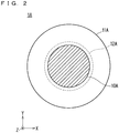
- FIG. 2 is a plan view illustrating a first mode of a high-voltage side electrode component 1 illustrated in FIG. 1 .
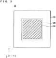
- FIG. 3 is a plan view illustrating a second mode of the high-voltage side electrode component 1 illustrated in FIG. 1 .
- the XYZ rectangular coordinate system is illustrated in each of FIGS. 1 to 3 .
- the high-voltage side electrode component 1 being a first electrode component and a ground side electrode component 2 being a second electrode component face each other.
- the ground side electrode component 2 is located below the high-voltage side electrode component 1.
- the high-voltage side electrode component 1 includes an electrode conductive film 10, an electrode main dielectric film 11 and an electrode additional dielectric film 12, and the ground side electrode component 2 includes an electrode conductive film 20, an electrode main dielectric film 21 and an electrode additional dielectric film 22.
- the electrode main dielectric film 11 is provided on the lower surface of the electrode conductive film 10, and the electrode additional dielectric film 12 is disposed below the electrode main dielectric film 11 at an upper main/additional inter-dielectric distance d21.
- the electrode main dielectric film 11 is provided, on the side of a discharge space 61 described later with respect to the electrode conductive film 10, adjacent to the electrode conductive film 10, and the electrode additional dielectric film 12 is provided, on the side of the discharge space 61 with respect to the electrode main dielectric film 11 at the upper main/additional inter-dielectric distance d21.
- the electrode conductive film 10 corresponds to a first electrode conductive film
- the electrode main dielectric film 11 corresponds to a first electrode main dielectric film
- the electrode additional dielectric film 12 corresponds to a first electrode additional dielectric film
- the upper main/additional inter-dielectric distance d21 corresponds to a first distance.
- a method of disposing the electrode additional dielectric film 12 below the electrode main dielectric film 11 for example, a method is adopted in which a gap being the upper main/additional inter-dielectric distance d21 between the electrode main dielectric film 11 and the electrode additional dielectric film 12 is provided with the use of a spacer or the like not illustrated.
- the electrode main dielectric film 21 is provided on the upper surface of the electrode conductive film 20, and the electrode additional dielectric film 22 is disposed above the electrode main dielectric film 21 at an lower main/additional inter-dielectric distance d22.
- the electrode main dielectric film 21 is provided, on the side of the discharge space 61 with respect to the electrode conductive film 20, adjacent to the electrode conductive film 20, and the electrode additional dielectric film 22 is provided, on the side of the discharge space 61 with respect to the electrode main dielectric film 21 at the lower main/additional inter-dielectric distance d22.
- the electrode conductive film 20 corresponds to a second electrode conductive film
- the electrode main dielectric film 21 corresponds to a second electrode main dielectric film
- the electrode additional dielectric film 22 corresponds to a second electrode additional dielectric film
- the lower main/additional inter-dielectric distance d22 corresponds to a second distance.
- a method of disposing the electrode additional dielectric film 22 above the electrode main dielectric film 21 for example, a method is adopted in which a gap being the lower main/additional inter-dielectric distance d22 between the electrode main dielectric film 21 and the electrode additional dielectric film 22 is provided with the use of a spacer or the like not illustrated.
- the electrode main dielectric film 11 (11A, 11B) includes the whole electrode conductive film 10 (10A, 10B) in a plan view in the XY plane, and has a formation area sufficiently larger than the electrode conductive film 10.
- the high-voltage side electrode component 1A includes a circular electrode conductive film 10A, an electrode main dielectric film 11A, and an electrode additional dielectric film 12A, each of which is circular in shape in a plan view.
- the center positions of the electrode conductive film 10A, the electrode main dielectric film 11A, and the electrode additional dielectric film 12A are aligned.
- the electrode main dielectric film 11A includes the whole electrode conductive film 10A in a plan view, and has a formation area larger than the electrode conductive film 10A.
- the high-voltage side electrode component 1B includes an electrode conductive film 10B, an electrode main dielectric film 11B, and an electrode additional dielectric film 12B, each of which is square in shape in a plan view.
- the center positions of the electrode conductive film 10B, the electrode main dielectric film 11B, and the electrode additional dielectric film 12B are aligned.
- the electrode main dielectric film 11B includes the whole electrode conductive film 10B in a plan view, and has a formation area larger than the electrode conductive film 10B.
- the electrode additional dielectric film 12 includes the electrode conductive film 10 in a plan view and has a formation area slightly larger than the electrode conductive film 10 and smaller than the electrode main dielectric film 11. In addition, it is desirable that the electrode additional dielectric film 12 has an area which is substantially the same as that of the electrode conductive film 10 in a plan view.
- the electrode additional dielectric film 12A includes the electrode conductive film 10A in a plan view and has a formation area slightly larger than the electrode conductive film 10A and smaller than the electrode main dielectric film 11A.
- the electrode additional dielectric film 12B includes the electrode conductive film 10B in a plan view and has a formation area slightly larger than the electrode conductive film 10B and smaller than the electrode main dielectric film 11B.
- the planar structure of the ground side electrode component 2 also has the following relationship as in the high-voltage side electrode component 1.
- the electrode main dielectric film 21 includes the whole electrode conductive film 20 in a plan view in the XY plane, and has a formation area larger than the electrode conductive film 20.
- the electrode additional dielectric film 22 includes the electrode conductive film 20 in a plan view and has a formation area slightly larger than the electrode conductive film 20 and smaller than the electrode main dielectric film 21. Note that it is desirable that the electrode additional dielectric film 22 has an area which is substantially the same as the electrode conductive film 20 in a plan view.
- the electrode main dielectric film 11 and the electrode main dielectric film 21 have substantially the same planar shape
- the electrode additional dielectric film 12 and the electrode additional dielectric film 22 have substantially the same planar shape
- the electrode conductive film 10 and the electrode conductive film 20 have substantially the same planar shape.
- the discharge space 61 exists that includes a region where the electrode conductive film 10 and the electrode conductive film 20 overlap in a plan view in the XY plane, in the main dielectric space where the electrode additional dielectric film 12 and the electrode additional dielectric film 22 face each other.
- the space defined by the upper main/additional inter-dielectric distance d21 between the electrode main dielectric film 11 and the electrode additional dielectric film 12 is an additional dielectric space 71.
- the additional dielectric space 71 corresponds to a first additional dielectric space.
- the space defined by the lower main/additional inter-dielectric distance d22 between the electrode main dielectric film 21 and the electrode additional dielectric film 22 is an additional dielectric space 72.
- the additional dielectric space 72 corresponds to a second additional dielectric space.
- a dielectric barrier discharge is caused in the discharge space 61 by applying an AC voltage between the electrode conductive film 10 and the electrode conductive film 20 from a high-frequency power source 9.
- the active gas generation apparatus of Embodiment 1 including the active gas generation electrode group 51 can activate the source gas supplied to the discharge space 61 to generate the active gas.
- the additional dielectric spaces 71 and 72 are set such that the dielectric barrier discharge is not caused in the respective additional dielectric spaces 71 and 72 when the dielectric barrier discharge is caused in the discharge space 61 in the main dielectric space.
- the active gas generation electrode group 51 satisfies the discharge classification requirements in which "no dielectric barrier discharge occurs in the respective additional dielectric spaces 71 and 72 when the dielectric barrier discharge is caused in the discharge space 61 in the main dielectric space".
- the main dielectric space is provided between the electrode main dielectric film 11 being the first electrode additional dielectric film and the electrode additional dielectric film 12 of the ground side electrode component 2 being the second electrode component.
- the discharge space 61 exists in the main dielectric space.
- the electrode additional dielectric film 12 includes the electrode conductive film 10 in a plan view and has a formation area larger than the electrode conductive film 10 and smaller than the electrode main dielectric film 11.
- the thermal stress in the electrode additional dielectric film 12 can be maintained at a low level because the electrode additional dielectric film 12 is heated in a relatively uniform manner due to the smaller formation area than the electrode main dielectric film 11.
- the electrode additional dielectric film 12 has almost the same forming area as the electrode conductive film 10, the electrode additional dielectric film 12 is heated almost uniformly when the dielectric barrier discharge occurs in the discharge space 61. And therefore, almost no thermal stress is occurred in the electrode additional dielectric film 12.
- the electrode main dielectric film 11 is located at a position at the upper main/additional inter-dielectric distance d21 from the electrode additional dielectric film 12; therefore, relatively less heat to be transmitted from the electrode additional dielectric film 12 to the electrode main dielectric film 11.
- the thermal conductivity of the gas is significantly lower than the thermal conductivity of the solid, and the upper main/additional inter-dielectric distance d21, which is the gap length of the additional dielectric space 71, is relatively short; therefore, it is presumed that the gas flow is small and the less heat is transmitted due to convection.
- the heat transmission form the discharge space 61 to the electrode main dielectric film 11 can be maintained at a low level by the addition of the electrode additional dielectric film 12, and the damage of the electrode main dielectric film 11 due to the thermal stress can be prevented.
- the heat transmission through the spacer can also reliably be suppressed.
- the damaging phenomenon due to thermal stress during the dielectric barrier discharge can be suppressed, with respect to the electrode additional dielectric film 12 and the electrode main dielectric film 11.
- the electrode main dielectric film 11 includes the electrode conductive film 10 in a plan view and has a larger forming area than the electrode conductive film 10 and the electrode additional dielectric film 12; therefore, the end portion of the electrode main dielectric film 11 and the end portion of the electrode conductive film 10 do not match. Therefore, occurrence of creeping discharge at the end portion of the high-voltage side electrode component 1 can be suppressed.
- the active gas generation apparatus of Embodiment 1 ensures to maintain the unobstructed occurrence state of the dielectric barrier discharge.
- the electrode conductive film 10 the electrode main dielectric film 11, the electrode additional dielectric film 12, the electrode conductive film 20, the electrode main dielectric film 21, and the electrode additional dielectric film 22 all adopt a flat plate structure. That is, the active gas generation electrode group 51 can be realized at a relatively moderate cost because an intricate structure is not required.
- the electrode additional dielectric film 22 includes the electrode conductive film 20 in a plan view and has a formation area slightly larger than the electrode conductive film 20 and smaller than the electrode main dielectric film 21.
- the thermal stress in the electrode additional dielectric film 22 can be maintained at a low level because the electrode additional dielectric film 22 is heated in a relatively uniform manner due to the smaller formation area than the electrode main dielectric film 21.
- the electrode additional dielectric film 22 has almost the same forming area as the electrode conductive film 20, the electrode additional dielectric film 22 is heated almost uniformly when the dielectric barrier discharge occurs. And therefore, almost no thermal stress is occurred in the electrode additional dielectric film 22.
- the electrode main dielectric film 21 is located at a position at the lower main/additional inter-dielectric distance d22 from the electrode additional dielectric film 22; therefore, relatively less heat to be transmitted from the electrode additional dielectric film 22 to the electrode main dielectric film 21.
- the damaging phenomenon due to thermal stress during the dielectric barrier discharge can be suppressed, with respect to the electrode additional dielectric film 22 and the electrode main dielectric film 21.
- the electrode main dielectric film 21 includes the electrode conductive film 20 in a plan view and has a larger forming area than the electrode conductive film 20; therefore, the end portion of the electrode conductive film 20 and the end portion of the electrode main dielectric film 21 do not match. Accordingly, the occurrence of creeping discharge at the end portion of the ground side electrode component 2 can further be suppressed.
- the active gas generation apparatus of Embodiment 1 ensures to maintain the unobstructed occurrence state of the dielectric barrier discharge.
- the active gas generation electrode group 51 of Embodiment 1 satisfies the discharge classification requirements in which "no dielectric barrier discharge occurs in the respective additional dielectric spaces 71 and 72 when the dielectric barrier discharge is caused in the discharge space 61 in the main dielectric space".
- parameters such as the upper main/additional inter-dielectric distance d21 and the lower main/additional inter-dielectric distance d22 are appropriately set so that the above discharge classification requirements can be satisfied.
- the above upper main/additional inter-dielectric distance d21 and the lower main/additional inter-dielectric distance d22 are setting target parameters to be set appropriately based on the discharge conditions.
- the discharge conditions include conditions such as the gas type, the atmospheric pressure of the discharge field (discharge space), and the material and thickness of the dielectric film.
- the setting target parameters are the upper main/additional inter-dielectric distance d21 and the lower main/additional inter-dielectric distance d22 as an example
- the setting processing for discharge restriction parameter will be described in detail which sets the value of the setting target parameter such that the above discharge classification requirements are satisfied.
- the relative permittivity and the film thickness of each of the electrode main dielectric films 11 and 21, the relative permittivity and the film thickness of each of the electrode additional dielectric films 12 and 22, and the gap length d61 of the discharge space 61, and the like are set in advance.
- ⁇ 11 being the main dielectric relative permittivity of the dielectric being a constituent material of the electrode main dielectric film 11 is set to "10", and the main dielectric film thickness is set to 1 mm.
- ⁇ 12 being the main dielectric relative permittivity of the dielectric being a constituent material of the electrode main dielectric film 21 is set to "10”, and the main dielectric film thickness t21 is set to 1 mm.
- ⁇ 1 being the additional dielectric relative permittivity of the dielectric being a constituent material of the electrode additional dielectric film 12 is set to "10”
- the additional dielectric film thickness t12 of the electrode additional dielectric film 12 is set to 0.5 mm
- ⁇ 22 being the additional dielectric relative permittivity of the dielectric being a constituent material of the electrode additional dielectric film 22 is set to "10”
- the additional dielectric film thickness t22 of the electrode additional dielectric film 22 is set to 0.5 mm.
- the film thicknesses of the electrode main dielectric films 11 and 21 and the electrode additional dielectric films 12 and 22 are uniform.
- the gap length d61 of the discharge space 61 is set to 1 mm
- the relative permittivity of the gas occupying the discharge space 61 and the additional dielectric spaces 71 and 72 is set to "1”
- the atmospheric pressure of the discharge space 61 is set to 760 torr.
- the voltage applied, by the high-frequency power source 9, between the electrode conductive film 10 and the electrode conductive film 20 is set to 10000 V.
- the upper main/additional inter-dielectric distances d21 and d22 are both set to 0.25 mm as the setting processing for discharge restriction parameters.
- the active gas generation electrode group 51 of Embodiment 1 satisfies the above discharge classification requirements. This point will be described in detail below.
- the voltage ratio applied to each of the electrode main dielectric film 11, the additional dielectric space 71, the electrode additional dielectric film 12, the discharge space 61, the electrode additional dielectric film 22, the additional dielectric space 72, and the electrode main dielectric film 21 can be calculated from the ratio of the respective capacitances.
- Capacitance is proportional to the (relative) permittivity divided by its thickness.
- the combined capacitance of the electrode main dielectric films 11 and 21 is C11
- the combined capacitance of the additional dielectric spaces 71 and 72 is C71
- the combined capacitance of the electrode additional dielectric films 12 and 22 is C12
- the capacitance of the discharge space 61 is C61.
- the values of the capacitances C11, C71, C12, and C61 are obtained from the following Equations (1) to (4).
- Equations (1) to (4) the capacitance C61 is set as the reference value "1".
- the voltage ratio ⁇ V11:V71:V12:V61 ⁇ over the four regions corresponding to the above-mentioned capacitances C11, C71, C12 and C61 is obtained as the reciprocal of the capacitance.
- the voltage value V11 indicates the voltage value applied to the combined region of the electrode main dielectric films 11 and 21, and the voltage value V71 indicates the voltage value applied to the combined region of the additional dielectric spaces 71 and 72. Further, the voltage value V12 indicates the voltage value applied to the combined region of the electrode additional dielectric films 12 and 22, and the voltage value V61 indicates the voltage value applied to the discharge space 61.
- V 11 : V 71 : V 12 : V 61 2 : 5 : 1 : 10
- Equation (5) the voltage value V12 is set as the reference value "1".
- the total voltage is dispersed in the additional dielectric spaces 71 and 72; therefore, the voltage ⁇ V71/2 ⁇ applied to each of the additional dielectric spaces 71 and 72 is about 1389 V.
- Embodiment 1 ensures the dielectric barrier discharge not to occur in the additional dielectric spaces 71 and 72, when 10000 V is applied between the electrode conductive films 10 and 20 to occur a dielectric barrier discharge in the discharge space 61.
- the above discharge classification requirements can be surely satisfied by performing the setting processing for discharge restriction parameter to set the upper main/additional inter-dielectric distance d21 and the lower main/additional inter-dielectric distance d22.
- the electrode conductive film 10, the electrode main dielectric film 11, the electrode additional dielectric film 12, and the upper main/additional inter-dielectric distance d21 are classed as a first electrode conductive film or the like, or "first group” and the electrode conductive film 20, the electrode main dielectric film 21, the electrode additional dielectric film 22, and the lower main/additional inter-dielectric distance d22 are classed as a second electrode conductive film or the like, or "second group”.
- first group and “second group” may be reversed. That is, the above-mentioned effect can be exhibited as it is if the electrode conductive film 10, the electrode main dielectric film 11, the electrode additional dielectric film 12, and the upper main/additional inter-dielectric distance d21 are classed as the "second group” and the electrode conductive film 20, the electrode main dielectric film 21, the electrode additional dielectric film 22, and the lower main/additional inter-dielectric distance d22 are classed as the "first group”.
- FIG. 4 is an explanatory diagram illustrating a structure of an active gas generation electrode group 52 in an active gas generation apparatus according to Embodiment 2 of the present disclosure and the peripheral portion thereof.
- the XYZ rectangular coordinate system is illustrated in FIG. 4 .
- the parts common to the active gas generation electrode group 51 described in Embodiment 1 are denoted by the same reference numerals and the description thereof will be omitted as appropriate, and the characteristics of the active gas generation electrode group 52 will be mainly described.
- the active gas generation electrode group 52 differs from the active gas generation electrode group 51 of Embodiment 1 in that the ground side electrode component 2 is replaced with the ground side electrode component 2X.
- the ground side electrode component 2X being the second electrode component includes only an electrode conductive film 20X being the second electrode conductive film.
- the electrode conductive film 20X has a planar shape similar to that of the electrode main dielectric film 11. That is, the electrode conductive film 20X includes the whole electrode additional dielectric film 12 in a plan view in the XY plane, and has a formation area larger than the electrode additional dielectric film 12.
- the electrode conductive film 20X may also have a planar shape similar to that of the electrode conductive film 10.
- the space between the electrode additional dielectric film 12 of the high-voltage side electrode component 1 and the electrode conductive film 20X of the ground side electrode component 2X is the main dielectric space, and a discharge space 62 exists in the main dielectric space.
- the discharge space 62 exists that includes a region where the electrode conductive film 10 and the electrode conductive film 20X overlap in a plan view in the XY plane in the main dielectric space where the electrode additional dielectric film 12 of the high-voltage side electrode constituent unit 1 and the electrode conductive film 20X of the ground side electrode constituent unit 2 face each other.
- the space defined by the upper main/additional inter-dielectric distance d21 between the electrode main dielectric film 11 and the electrode additional dielectric film 12 is an additional dielectric space 71 (the first additional dielectric space) in the active gas generation electrode group 52.
- the ground side electrode component 2X does not include a dielectric film corresponding to the electrode additional dielectric film 22; therefore, no second additional dielectric space exists.
- a dielectric barrier discharge is caused in the discharge space 62 by applying an AC voltage between the electrode conductive film 20X and the electrode conductive film 10 from a high-frequency power source 9.
- the active gas generation apparatus of Embodiment 2 including the active gas generation electrode group 52 can activate the source gas supplied to the discharge space 62 to generate the active gas.
- the active gas generation electrode group 52 is set to satisfy the discharge restriction requirements in that "the dielectric barrier discharge is not caused in the additional dielectric space 71 when the dielectric barrier discharge is caused in the discharge space 62 in the main dielectric space".
- Embodiment 2 the discharge classification requirements can be surely satisfied as is the same with Embodiment 1 by performing the setting processing for discharge restriction parameter.
- the principle of the setting processing for discharge restriction parameter is the same as that described in Embodiment 1: therefore, the specific description of the setting processing for discharge restriction parameter in Embodiment 2 will be omitted.
- the active gas generation electrode group 52 includes a high-voltage side electrode component 1 having the same structure as the active gas generation electrode group 51 of Embodiment 1; therefore, the same effect as Embodiment 1 is exhibited with the high-voltage side electrode component 1.
- the electrode conductive film 10 the electrode main dielectric film 11, the electrode additional dielectric film 12, and the electrode conductive film 20X all adopt a flat plate structure. That is, the active gas generation electrode group 52 can be realized at a relatively moderate cost because an intricate structure is not required.
- the space between the electrode additional dielectric film 12 and the electrode conductive film 20X is the main dielectric space, and the discharge space 62 exists in the main dielectric space.
- the damaging phenomenon due to thermal stress during the dielectric barrier discharge can be suppressed, with respect to the electrode main dielectric film 11 and the electrode additional dielectric film 12 as is the same with Embodiment 1.
- the ground side electrode component 2X is composed of only the electrode conductive film 20X.
- the damaging phenomenon due to thermal stress is suppressed, with respect the electrode conductive film 20X that is the discharge surface of the discharge space 62.
- FIG. 5 is an explanatory diagram illustrating a structure of an active gas generation electrode group 53 in an active gas generation apparatus according to Embodiment 3 of the present disclosure and the peripheral portion thereof.
- the XYZ rectangular coordinate system is illustrated in FIG. 5 .
- the parts common to the active gas generation electrode group 51 described in Embodiment 1 are denoted by the same reference numerals and the description thereof will be omitted as appropriate, and the characteristics of the active gas generation electrode group 53 will be mainly described.
- the active gas generation electrode group 53 differs from the active gas generation electrode group 51 of Embodiment 1 in that the ground side electrode component 2 is replaced with the ground side electrode component 2Y.
- the electrode additional dielectric film 22 being the second electrode additional dielectric film is provided, above the electrode conductive film 20Y being the second electrode conductive film, at a lower conductor/additional inter-dielectric distance d32 (the second distance) with respect to the electrode conductive film 20Y being the second electrode conductive film.
- the electrode conductive film 20Y has a planar shape similar to that of the electrode main dielectric film 11. That is, the electrode conductive film 20Y includes the whole electrode additional dielectric film 22 in a plan view in the XY plane, and has a formation area larger than the electrode additional dielectric film 22.
- the electrode additional dielectric film 12 and the electrode additional dielectric film 22 have substantially the same planar shape.
- the electrode conductive film 20Y may also have a planar shape similar to that of the electrode conductive film 10.
- a method of disposing the electrode additional dielectric film 22 above the electrode conductive film 20Y for example, it is conceivable to adopt a method in which a gap being the lower conductor/additional inter-dielectric distance d32 between the electrode conductive film 20Y and the electrode additional dielectric film 22 is provided with the use of a spacer or the like not illustrated.
- the space between the electrode additional dielectric film 12 of the high-voltage side electrode component 1 and the electrode additional dielectric film 22 of the ground side electrode component 2Y is the main dielectric space, and a discharge space 63 exists in the main dielectric space.
- the discharge space 63 exists that includes a region where the electrode conductive film 10 and the electrode conductive film 20Y overlap in a plan view in the XY plane in the main dielectric space where the electrode additional dielectric film 12 of the high-voltage side electrode constituent unit 1 and the electrode additional dielectric film 22 of the ground side electrode constituent unit 2 face each other.
- the space defined by the upper main/additional inter-dielectric distance d21 (the first distance) between the electrode main dielectric film 11 and the electrode additional dielectric film 12 is an additional dielectric space 71 (the first additional dielectric space) in the active gas generation electrode group 53.
- the space defined by the lower conductor/additional inter-dielectric distance d32 (the second distance) between the electrode conductive film 20Y and the electrode additional dielectric film 22 is an additional dielectric space 72C (the second additional dielectric space).
- a dielectric barrier discharge is caused in the discharge space 63 by applying an AC voltage between the electrode conductive film 10 and the electrode conductive film 20Y from a high-frequency power source 9.
- the active gas generation apparatus of Embodiment 3 including the active gas generation electrode group 53 can activate the source gas supplied to the discharge space 63 to generate the active gas.
- the active gas generation electrode group 53 is configured to satisfy the discharge restriction requirements in that "the dielectric barrier discharge is not caused in each of the additional dielectric spaces 71 and 72C when the dielectric barrier discharge is caused in the discharge space 63 in the main dielectric space".
- Embodiment 3 the discharge classification requirements can be surely satisfied as is the same with Embodiment 1 by performing the setting processing for discharge restriction parameter.
- the principle of the setting processing for discharge restriction parameter is the same as that described in Embodiment 1: therefore, the specific description of the setting processing for discharge restriction parameter in Embodiment 3 will be omitted.
- the active gas generation electrode group 53 includes a high-voltage side electrode component 1 having the same structure as the active gas generation electrode group 51 of Embodiment 1; therefore, the same effect as Embodiment 1 is exhibited with the high-voltage side electrode component 1 and the electrode additional dielectric film 22 of the ground side electrode component 2Y.
- the electrode conductive film 10 the electrode main dielectric film 11, the electrode additional dielectric film 12, the electrode conductive film 20Y, and the electrode additional dielectric film 22 all adopt a flat plate structure. That is, the active gas generation electrode group 53 can be realized at a relatively moderate cost because an intricate structure is not required.
- the electrode additional dielectric film 22 being the second electrode additional dielectric film is located at a position at the lower conductor/additional inter-dielectric distance d32 (the second distance) from the electrode conductive film 20Y being the second electrode conductive film.
- the electrode additional dielectric film 22 is disposed at the lower conductor/additional inter-dielectric distance d32 from the electrode conductive film 20Y without contacting the electrode conductive film 20Y; therefore, relatively less heat to be transmitted from the electrode conductive film 20Y to the electrode additional dielectric film 22.
- the damaging phenomenon due to thermal stress during the dielectric barrier discharge can be suppressed, with respect to the electrode additional dielectric film 22.
- discharge spaces 61 and 63 are formed between the electrode additional dielectric film 12 and the electrode additional dielectric film 22.
- the electrode main dielectric film 11 (and the electrode main dielectric film 21) that is not directly related with the discharge spaces 61 and 63 can have an arbitrary intricate shape by using a constituent material having good workability.
- a material having great sputtering resistance (typically a material that is hard and difficult to process into a complicated shape) is to be adoptable, or application of a substance having catalytic properties to the surfaces of the electrode additional dielectric films 12 and 22, or other treatments, is to be adoptable.
- An electrode structure may also be adopted in which a third electrode additional dielectric film which is subjected to the application of catalyst or other treatments, is further disposed in the discharge space 61 (63) between the electrode additional dielectric films 12 and 22 to raise the contact probability between the catalyst and the gas (source gas).
- each of the active gas generation electrode groups 51 to 53 even if the electrode additional dielectric film 12 (and 22) is damaged by the dielectric barrier discharge, the damage is restricted only to the electrode additional dielectric film 12. Therefore, by adopting a structure in which the replacement of the electrode additional dielectric film 12 is facilitated, an increase in the longevity of the active gas generation apparatus is achievable.
- the electrode main dielectric film 11 (and 21) requires a certain thickness (strength) because it is a structure, whereas the electrode additional dielectric film 12 (and 22) may be extremely thin.
- the electrode additional dielectric film 12 is produced using bulk ceramics as a constituent material, the difficulty lies in making it thinner; therefore, the constituent material of the electrode additional dielectric film 12 is limited. In addition, in some cases, a problem arises that impurities are contained in order to improve the workability of the electrode additional dielectric film 12.
- the electrode additional dielectric film 12 may be formed such that an insulating material (dielectric) is formed on a sheet-shaped metal film by a CVD method or a sputtering method so that the entire metal film is covered with the insulating material.
- an insulating material dielectric
- the electrode additional dielectric film 12 (and 22) there is an advantageous feature that products having various compositions and high purity can be produced as the electrode additional dielectric film 12 (and 22).
Landscapes
- Physics & Mathematics (AREA)
- Engineering & Computer Science (AREA)
- Plasma & Fusion (AREA)
- Spectroscopy & Molecular Physics (AREA)
- Chemical & Material Sciences (AREA)
- Analytical Chemistry (AREA)
- Plasma Technology (AREA)
Abstract
Description
- The present disclosure relates to an active gas generation apparatus including an electrode group of the parallel-plate type in which a first and a second electrode components face each other, and using a dielectric barrier discharge in the electrode group, and particularly to a structure of the electrode group.
- As an active gas generation apparatus that activates a source gas supplied to a discharge space to generate an active gas, there are the active gas generation apparatuses having an electrode group of parallel-plate type in which the first and the second electrode components face each other.
- The active gas generation apparatus causes a dielectric barrier discharge in the discharge space of the electrode group and activates the source gas supplied to the discharge space to generate the active gas. As such an active gas generation apparatus, for example, there is a discharge plasma processing apparatus disclosed in Patent Document 1.
-
FIG. 6 is an explanatory diagram illustrating a configuration of an active gasgeneration electrode group 59X of parallel-plate type used in a conventional active gas generation apparatus and the peripheral portion thereof. The XYZ rectangular coordinate system is illustrated inFIG. 6 . - As illustrated in
FIG. 6 , a high-voltageside electrode component 101 and a groundside electrode component 102 face each other. In the configuration illustrated inFIG. 6 , the groundside electrode component 102 is located below the high-voltageside electrode component 101. - The high-voltage
side electrode component 101 includes an electrode conductive film 110X and an electrodedielectric film 111, and the groundside electrode component 102 includes an electrodeconductive film 120X and an electrodedielectric film 121. - In the high-voltage
side electrode component 101, an electrodedielectric film 111 is provided on the lower surface of the electrode conductive film 110X. In the ground voltageside electrode component 102, an electrodedielectric film 121 is provided on the upper surface of the electrodeconductive film 120X. - The electrode
dielectric film 111 includes the whole electrode conductive film 110X in a plan view in the XY plane, and has a formation area sufficiently larger than the electrode conductive film 110X. - The electrode
dielectric film 121 includes the whole electrodeconductive film 120X in a plan view in the XY plane, and has a formation area sufficiently larger than the electrodeconductive film 120X. - In the active gas
generation electrode group 59X, adischarge space 69X exists that includes a region where the electrode conductive film 110X and the electrodeconductive film 120X overlap in a plan view in the XY plane in a main dielectric space where the electrodedielectric film 111 and the electrodedielectric film 121 face each other. Then, as illustrated inFIG. 6 , the space other than thedischarge space 69X in the main dielectric space is anon-discharge space 79. - For the active gas
generation electrode group 59X having such a configuration, a dielectric barrier discharge is caused in thedischarge space 69X by applying an AC voltage between the electrode conductive film 110 and the electrode conductive film 120 from a high-frequency power source 109. - [Patent Document 1]
Japanese Patent Application Laid-Open No. 2007-144244 - In the conventional active gas
generation electrode group 59X, the surface of each of the electrodedielectric films discharge space 69X is heated by collisions of ions and electrons generated by the dielectric barrier discharge caused in thedischarge space 69X. - Meanwhile, in the above main dielectric space, the surface of each of the electrode
dielectric films non-discharge space 79 in which the dielectric barrier discharge is not caused, is not heated because no collisions of ions and electrons occur. - As a constituent material of the electrode
dielectric films dielectric films - When the dielectric barrier discharge occurs, a large temperature difference occurs between the
non-discharge space 79 side and thedischarge space 69X side on the surfaces of the electrodedielectric films dielectric films - The thermal stress causes a problem of damage in that the electrode
dielectric films non-discharge space 79 and thedischarge space 69X. - Further, the electrode
dielectric films discharge space 69X, ending up deriving the phenomenon of causing of the arc discharge in thedischarge space 69X. Hereinafter, the phenomenon is referred to as "phenomenon of disabling dielectric barrier discharge". -
FIG. 7 is an explanatory diagram illustrating a configuration of a conventional active gasgeneration electrode group 59Y of parallel-plate type and the peripheral portion thereof. The XYZ rectangular coordinate system is illustrated inFIG. 7 . - Hereinafter, the active gas
generation electrode group 59Y will be described mainly on the points different from the active gasgeneration electrode group 59X. - The high-voltage
side electrode component 101 includes an electrodeconductive film 110Y and an electrodedielectric film 111, and the groundside electrode component 102 includes an electrodeconductive film 120Y and an electrodedielectric film 121. - In the high-voltage
side electrode component 101, an electrodedielectric film 111 is provided on the lower surface of the electrodeconductive film 110Y. In the ground voltageside electrode component 102, an electrodedielectric film 121 is provided on the upper surface of the electrodeconductive film 120Y. - The electrode
conductive film 110Y is formed in a shape that matches the electrodedielectric film 111 in a plan view in the XY plane, and the electrodeconductive film 120Y is formed in a shape that matches the electrodedielectric film 121 in a plan view in the XY plane. - In the active gas
generation electrode group 59Y, adischarge space 69Y exists that includes a region where the electrodeconductive film 110Y and the electrodeconductive film 120Y overlap in a plan view in the XY plane in a main dielectric space where the electrodedielectric film 111 and the electrodedielectric film 121 face each other. And, the main dielectric space and thedischarge space 69Y substantially match with each other; therefore, no non-discharge space substantially exists in the main dielectric space. - Consequently, unlike in the active gas
generation electrode group 59X, no temperature difference occurs in the electrodedielectric films generation electrode group 59Y; therefore, no thermal stress occurs in the electrodedielectric films - As a result, unlike the active gas
generation electrode group 59X, no damage of the electrodedielectric films generation electrode group 59Y. - However, in the active gas
generation electrode group 59Y, each of the end surfaces of the electrodedielectric film 111 and the electrodeconductive film 110Y matches with each other, and each of the end surfaces of the electrodedielectric film 121 and the electrodeconductive film 120Y matches with each other. - Therefore, a separate problem arises in that the maintenance of the dielectric discharge barrier is aborted in the
discharge space 69Y as a result of, if a creeping discharge CD is caused between the end portions of the high-voltageside electrode component 101 and the groundside electrode component 102 and the creeping discharge CD leads to arc discharge in some cases. - Meanwhile, in the discharge plasma processing apparatus disclosed in Patent Document 1, the electrode structure is adopted in which paths through which the processing gas flows are included in a laminated body in which the electrode conductive films (discharge electrodes) and electrode dielectric films (dielectrics) are alternately laminated and the electrode conductive films are formed to have uneven front and back surfaces as the above electrode conductive films. That is, the above discharge plasma processing apparatus adopts the electrode structure in which one plate dielectric is interposed between a pair of electrode conductive films (discharge electrodes), each of which has an uneven shape, facing each other.
- In this manner, in the above discharge plasma processing apparatus, the electric field is prevented from concentrating at the portions being contact with the convex portions of the electrode conductive films in the electrode dielectric films by devising the shape of the electrode conductive films.
- As a result, the above discharge plasma processing apparatus prevents the phenomenon of disabling dielectric barrier discharge from deriving by suppressing the generation of a high temperature field due to electric field concentration in the electrode dielectric films.
- However, the electrode structure adopted in the above discharge plasma processing apparatus is mainly intended for the prevention of the above phenomenon of disabling dielectric barrier discharge, and is not intended for addressing the problem of the damage in the electrode dielectric films due to the generation of the thermal stress described in the active gas
generation electrode group 59X inFIG. 6 . - In addition, the prerequisite for the above discharge plasma processing apparatus is that the electrode conductive films and the electrode dielectric films are alternately laminated. For this reason, unlike the active gas
generation electrode groups FIGS. 6 and7 , the electrode structure in which thedischarge spaces dielectric films - In addition, there has been a problem with the above discharge plasma processing apparatus in that an extra manufacturing cost is required since the structure of the electrode conductive films is provided with unevenness.
- An object of the present disclosure is to solve the above problems and provide an active gas generation apparatus having an electrode structure that prevents the damaging phenomenon of the electrode dielectric films at a relatively moderate cost. Means to Solve the Problem
- An active gas generation apparatus according to the present disclosure is an active gas generation apparatus configured to generate an active gas obtained by activating a source gas supplied to a discharge space. The active gas generation apparatus includes a first electrode component, and a second electrode component provided to face the first electrode component, in which the first electrode component includes a first electrode conductive film, the second electrode component includes a second electrode conductive film, the discharge space including a region where the first and the second electrode conductive films overlap in a plan view in a main dielectric space where the first and the second electrode components face each other, in which an AC voltage is applied between the first and the second electrode conductive films exists, the first electrode component further includes a first electrode main dielectric film provided, on a side of the discharge space with respect to the first electrode conductive film, adjacent to the first electrode conductive film, and a first additional electrode dielectric film provided, on a side of the discharge space with respect to the first electrode main dielectric film, at a first distance with respect to the first electrode main dielectric film, a first additional dielectric space is provided between the first electrode main dielectric film and the first electrode additional dielectric film, the main dielectric space is provided between the first electrode additional dielectric film and the second electrode component, the first additional dielectric space is set such that a dielectric barrier discharge is not caused in the first additional dielectric space when the dielectric barrier discharge is caused in the discharge space in the main dielectric space, the first electrode main dielectric film includes the first electrode conductive film in a plan view, and has a formation area larger than the first electrode conductive film, and the first electrode additional dielectric film includes the first electrode conductive film in a plan view, and has a formation area larger than the first electrode conductive film and smaller than the first electrode main dielectric film.
- In the present disclosure, the main dielectric space is provided between the first electrode additional dielectric film and the second electrode component. The discharge space exists in the main dielectric space.
- The first electrode additional dielectric film includes the first electrode conductive film in a plan view and has a formation area larger than the first electrode conductive film and smaller than the first electrode main dielectric film.
- Therefore, when the dielectric barrier discharge is caused in the discharge space, the active gas generation apparatus of the present disclosure maintains the thermal stress at a low level because the first electrode additional dielectric film is heated in a relatively uniform manner due to the smaller formation area than the first electrode main dielectric film.
- In addition, the first electrode main dielectric film is located at a position at the first distance from the first electrode additional dielectric film; therefore, relatively less heat to be transmitted from the first electrode additional dielectric film to the first electrode main dielectric film.
- As a result, in the active gas generation apparatus of the present disclosure, the damaging phenomenon due to thermal stress during the dielectric barrier discharge can be suppressed, with respect to the first electrode additional dielectric film and the first electrode main dielectric film.
- Further, the first electrode main dielectric film includes the first electrode conductive film in a plan view and has a larger forming area than the first electrode conductive film and the first electrode additional dielectric film; therefore, the occurrence of creeping discharge at between the end portion of the first electrode conductive film and the end portion of the second electrode conductive film can be effectively suppressed.
- Therefore, the active gas generation apparatus of the present disclosure ensures to maintain the unobstructed occurrence state of the dielectric barrier discharge.
- In addition, the electrode group adopted in the active gas generation apparatus of the present disclosure can be realized at a relatively moderate cost because all the first electrode conductive film, the first electrode main dielectric film, the first additional dielectric film, and the second electrode conductive film are not required to have an intricate structure.
- The explicit purpose, feature, phase, and advantage of the present invention will be described in detail hereunder with attached drawings.
-
- [
FIG. 1 ] An explanatory diagram illustrating a structure of an active gas generation electrode group in an active gas generation apparatus according to Embodiment 1. - [
FIG. 2 ] A plan view illustrating a first mode of a high-voltage side electrode component illustrated inFIG. 1 . - [
FIG. 3 ] A plan view illustrating a second mode of the high-voltage side electrode component illustrated inFIG. 1 . - [
FIG. 4 ] An explanatory diagram illustrating a structure of an active gas generation electrode group in an active gas generation apparatus according to Embodiment 2. - [
FIG. 5 ] An explanatory diagram illustrating a structure of an active gas generation electrode group in an active gas generation apparatus according to Embodiment 3. - [
FIG. 6 ] is an explanatory diagram illustrating a configuration of a conventional active gas generation electrode group of parallel-plate type (part 1). - [
FIG. 7 ] is an explanatory diagram illustrating a configuration of a conventional active gas generation electrode group of parallel-plate type (part 2). -
FIG. 1 is an explanatory diagram illustrating a structure of an active gas generation electrode group in an active gas generation apparatus according to Embodiment 1 of the present disclosure and the peripheral portion thereof.FIG. 2 is a plan view illustrating a first mode of a high-voltage side electrode component 1 illustrated inFIG. 1 .FIG. 3 is a plan view illustrating a second mode of the high-voltage side electrode component 1 illustrated inFIG. 1 . The XYZ rectangular coordinate system is illustrated in each ofFIGS. 1 to 3 . - As illustrated in
FIG. 1 , the high-voltage side electrode component 1 being a first electrode component and a ground side electrode component 2 being a second electrode component face each other. Specifically, the ground side electrode component 2 is located below the high-voltage side electrode component 1. - The high-voltage side electrode component 1 includes an electrode
conductive film 10, an electrode main dielectric film 11 and an electrodeadditional dielectric film 12, and the ground side electrode component 2 includes an electrode conductive film 20, an electrode main dielectric film 21 and an electrodeadditional dielectric film 22. - In the high-voltage side electrode component 1, the electrode main dielectric film 11 is provided on the lower surface of the electrode
conductive film 10, and the electrodeadditional dielectric film 12 is disposed below the electrode main dielectric film 11 at an upper main/additional inter-dielectric distance d21. - That is, the electrode main dielectric film 11 is provided, on the side of a
discharge space 61 described later with respect to the electrodeconductive film 10, adjacent to the electrodeconductive film 10, and the electrodeadditional dielectric film 12 is provided, on the side of thedischarge space 61 with respect to the electrode main dielectric film 11 at the upper main/additional inter-dielectric distance d21. - Here, the electrode
conductive film 10 corresponds to a first electrode conductive film, the electrode main dielectric film 11 corresponds to a first electrode main dielectric film, the electrodeadditional dielectric film 12 corresponds to a first electrode additional dielectric film, and the upper main/additional inter-dielectric distance d21 corresponds to a first distance. - As a method of disposing the electrode
additional dielectric film 12 below the electrode main dielectric film 11, for example, a method is adopted in which a gap being the upper main/additional inter-dielectric distance d21 between the electrode main dielectric film 11 and the electrodeadditional dielectric film 12 is provided with the use of a spacer or the like not illustrated. - In the ground side electrode component 2, the electrode main dielectric film 21 is provided on the upper surface of the electrode conductive film 20, and the electrode
additional dielectric film 22 is disposed above the electrode main dielectric film 21 at an lower main/additional inter-dielectric distance d22. - That is, the electrode main dielectric film 21 is provided, on the side of the
discharge space 61 with respect to the electrode conductive film 20, adjacent to the electrode conductive film 20, and the electrodeadditional dielectric film 22 is provided, on the side of thedischarge space 61 with respect to the electrode main dielectric film 21 at the lower main/additional inter-dielectric distance d22. - Here, the electrode conductive film 20 corresponds to a second electrode conductive film, the electrode main dielectric film 21 corresponds to a second electrode main dielectric film, the electrode
additional dielectric film 22 corresponds to a second electrode additional dielectric film, and the lower main/additional inter-dielectric distance d22 corresponds to a second distance. - As a method of disposing the electrode
additional dielectric film 22 above the electrode main dielectric film 21, for example, a method is adopted in which a gap being the lower main/additional inter-dielectric distance d22 between the electrode main dielectric film 21 and the electrodeadditional dielectric film 22 is provided with the use of a spacer or the like not illustrated. - The electrode main dielectric film 11 (11A, 11B) includes the whole electrode conductive film 10 (10A, 10B) in a plan view in the XY plane, and has a formation area sufficiently larger than the electrode
conductive film 10. - For example, in the first mode illustrated in
FIG. 2 , the high-voltageside electrode component 1A includes a circular electrodeconductive film 10A, an electrode maindielectric film 11A, and an electrode additionaldielectric film 12A, each of which is circular in shape in a plan view. When viewed in a plan view in the XY plane, the center positions of the electrodeconductive film 10A, the electrode maindielectric film 11A, and the electrode additionaldielectric film 12A are aligned. - And, the electrode main
dielectric film 11A includes the whole electrodeconductive film 10A in a plan view, and has a formation area larger than the electrodeconductive film 10A. - Further, in the second mode illustrated in
FIG. 3 , the high-voltageside electrode component 1B includes an electrodeconductive film 10B, an electrode maindielectric film 11B, and an electrode additionaldielectric film 12B, each of which is square in shape in a plan view. When viewed in a plan view in the XY plane, the center positions of the electrodeconductive film 10B, the electrode maindielectric film 11B, and the electrode additionaldielectric film 12B are aligned. - And, the electrode main
dielectric film 11B includes the whole electrodeconductive film 10B in a plan view, and has a formation area larger than the electrodeconductive film 10B. - Returning to
FIG. 1 , the electrodeadditional dielectric film 12 includes the electrodeconductive film 10 in a plan view and has a formation area slightly larger than the electrodeconductive film 10 and smaller than the electrode main dielectric film 11. In addition, it is desirable that the electrodeadditional dielectric film 12 has an area which is substantially the same as that of the electrodeconductive film 10 in a plan view. - For example, in the first mode illustrated in
FIG. 2 , the electrode additionaldielectric film 12A includes the electrodeconductive film 10A in a plan view and has a formation area slightly larger than the electrodeconductive film 10A and smaller than the electrode maindielectric film 11A. - Further, in the second mode illustrated in
FIG. 3 , the electrode additionaldielectric film 12B includes the electrodeconductive film 10B in a plan view and has a formation area slightly larger than the electrodeconductive film 10B and smaller than the electrode maindielectric film 11B. - The planar structure of the ground side electrode component 2 also has the following relationship as in the high-voltage side electrode component 1.
- The electrode main dielectric film 21 includes the whole electrode conductive film 20 in a plan view in the XY plane, and has a formation area larger than the electrode conductive film 20.
- The electrode
additional dielectric film 22 includes the electrode conductive film 20 in a plan view and has a formation area slightly larger than the electrode conductive film 20 and smaller than the electrode main dielectric film 21. Note that it is desirable that the electrodeadditional dielectric film 22 has an area which is substantially the same as the electrode conductive film 20 in a plan view. - Further, the electrode main dielectric film 11 and the electrode main dielectric film 21 have substantially the same planar shape, the electrode
additional dielectric film 12 and the electrodeadditional dielectric film 22 have substantially the same planar shape, and the electrodeconductive film 10 and the electrode conductive film 20 have substantially the same planar shape. - In such an active gas
generation electrode group 51, thedischarge space 61 exists that includes a region where the electrodeconductive film 10 and the electrode conductive film 20 overlap in a plan view in the XY plane, in the main dielectric space where the electrodeadditional dielectric film 12 and the electrodeadditional dielectric film 22 face each other. - The space defined by the upper main/additional inter-dielectric distance d21 between the electrode main dielectric film 11 and the electrode
additional dielectric film 12 is anadditional dielectric space 71. Theadditional dielectric space 71 corresponds to a first additional dielectric space. - The space defined by the lower main/additional inter-dielectric distance d22 between the electrode main dielectric film 21 and the electrode
additional dielectric film 22 is anadditional dielectric space 72. Theadditional dielectric space 72 corresponds to a second additional dielectric space. - For the active gas
generation electrode group 51 having such a configuration, a dielectric barrier discharge is caused in thedischarge space 61 by applying an AC voltage between the electrodeconductive film 10 and the electrode conductive film 20 from a high-frequency power source 9. - As a result, the active gas generation apparatus of Embodiment 1 including the active gas
generation electrode group 51 can activate the source gas supplied to thedischarge space 61 to generate the active gas. - Further, the additional
dielectric spaces dielectric spaces discharge space 61 in the main dielectric space. - That is, the active gas
generation electrode group 51 satisfies the discharge classification requirements in which "no dielectric barrier discharge occurs in the respective additionaldielectric spaces discharge space 61 in the main dielectric space". - In the active gas
generation electrode group 51 of Embodiment 1, the main dielectric space is provided between the electrode main dielectric film 11 being the first electrode additional dielectric film and the electrodeadditional dielectric film 12 of the ground side electrode component 2 being the second electrode component. Thedischarge space 61 exists in the main dielectric space. - The electrode
additional dielectric film 12 includes the electrodeconductive film 10 in a plan view and has a formation area larger than the electrodeconductive film 10 and smaller than the electrode main dielectric film 11. - Therefore, when the dielectric barrier discharge is caused in the
discharge space 61, the thermal stress in the electrodeadditional dielectric film 12 can be maintained at a low level because the electrodeadditional dielectric film 12 is heated in a relatively uniform manner due to the smaller formation area than the electrode main dielectric film 11. - For example, if the electrode
additional dielectric film 12 has almost the same forming area as the electrodeconductive film 10, the electrodeadditional dielectric film 12 is heated almost uniformly when the dielectric barrier discharge occurs in thedischarge space 61. And therefore, almost no thermal stress is occurred in the electrodeadditional dielectric film 12. - In addition, the electrode main dielectric film 11 is located at a position at the upper main/additional inter-dielectric distance d21 from the electrode
additional dielectric film 12; therefore, relatively less heat to be transmitted from the electrodeadditional dielectric film 12 to the electrode main dielectric film 11. - Furthermore, the thermal conductivity of the gas is significantly lower than the thermal conductivity of the solid, and the upper main/additional inter-dielectric distance d21, which is the gap length of the
additional dielectric space 71, is relatively short; therefore, it is presumed that the gas flow is small and the less heat is transmitted due to convection. - Accordingly, the heat transmission form the
discharge space 61 to the electrode main dielectric film 11 can be maintained at a low level by the addition of the electrodeadditional dielectric film 12, and the damage of the electrode main dielectric film 11 due to the thermal stress can be prevented. - Further, by adopting quartz having a relatively low thermal conductivity as a constituent material of the spacer that defines the upper main/additional inter-dielectric distance d21, the heat transmission through the spacer can also reliably be suppressed.
- As a result, in the active gas generation apparatus of Embodiment 1, the damaging phenomenon due to thermal stress during the dielectric barrier discharge can be suppressed, with respect to the electrode
additional dielectric film 12 and the electrode main dielectric film 11. - Further, the electrode main dielectric film 11 includes the electrode
conductive film 10 in a plan view and has a larger forming area than the electrodeconductive film 10 and the electrodeadditional dielectric film 12; therefore, the end portion of the electrode main dielectric film 11 and the end portion of the electrodeconductive film 10 do not match. Therefore, occurrence of creeping discharge at the end portion of the high-voltage side electrode component 1 can be suppressed. - Therefore, the active gas generation apparatus of Embodiment 1 ensures to maintain the unobstructed occurrence state of the dielectric barrier discharge.
- In addition, in the active gas
generation electrode group 51, the electrodeconductive film 10, the electrode main dielectric film 11, the electrodeadditional dielectric film 12, the electrode conductive film 20, the electrode main dielectric film 21, and the electrodeadditional dielectric film 22 all adopt a flat plate structure. That is, the active gasgeneration electrode group 51 can be realized at a relatively moderate cost because an intricate structure is not required. - In Embodiment 1, the electrode
additional dielectric film 22 includes the electrode conductive film 20 in a plan view and has a formation area slightly larger than the electrode conductive film 20 and smaller than the electrode main dielectric film 21. - Therefore, when the dielectric barrier discharge is caused in the
discharge space 61, the thermal stress in the electrodeadditional dielectric film 22 can be maintained at a low level because the electrodeadditional dielectric film 22 is heated in a relatively uniform manner due to the smaller formation area than the electrode main dielectric film 21. - For example, if the electrode
additional dielectric film 22 has almost the same forming area as the electrode conductive film 20, the electrodeadditional dielectric film 22 is heated almost uniformly when the dielectric barrier discharge occurs. And therefore, almost no thermal stress is occurred in the electrodeadditional dielectric film 22. - In addition, the electrode main dielectric film 21 is located at a position at the lower main/additional inter-dielectric distance d22 from the electrode
additional dielectric film 22; therefore, relatively less heat to be transmitted from the electrodeadditional dielectric film 22 to the electrode main dielectric film 21. - As a result, in the active gas generation apparatus of Embodiment 1, the damaging phenomenon due to thermal stress during the dielectric barrier discharge can be suppressed, with respect to the electrode
additional dielectric film 22 and the electrode main dielectric film 21. - Further, the electrode main dielectric film 21 includes the electrode conductive film 20 in a plan view and has a larger forming area than the electrode conductive film 20; therefore, the end portion of the electrode conductive film 20 and the end portion of the electrode main dielectric film 21 do not match. Accordingly, the occurrence of creeping discharge at the end portion of the ground side electrode component 2 can further be suppressed.
- Therefore, the active gas generation apparatus of Embodiment 1 ensures to maintain the unobstructed occurrence state of the dielectric barrier discharge.
- The active gas
generation electrode group 51 of Embodiment 1 satisfies the discharge classification requirements in which "no dielectric barrier discharge occurs in the respective additionaldielectric spaces discharge space 61 in the main dielectric space". - That is, in Embodiment 1, parameters, such as the upper main/additional inter-dielectric distance d21 and the lower main/additional inter-dielectric distance d22 are appropriately set so that the above discharge classification requirements can be satisfied.
- The above upper main/additional inter-dielectric distance d21 and the lower main/additional inter-dielectric distance d22 are setting target parameters to be set appropriately based on the discharge conditions. The discharge conditions include conditions such as the gas type, the atmospheric pressure of the discharge field (discharge space), and the material and thickness of the dielectric film.
- Here, taking the case where the setting target parameters are the upper main/additional inter-dielectric distance d21 and the lower main/additional inter-dielectric distance d22 as an example, the setting processing for discharge restriction parameter will be described in detail which sets the value of the setting target parameter such that the above discharge classification requirements are satisfied.
- In the above case, the relative permittivity and the film thickness of each of the electrode main dielectric films 11 and 21, the relative permittivity and the film thickness of each of the electrode additional
dielectric films discharge space 61, and the like are set in advance. - Here, in the active gas
generation electrode group 51 illustrated inFIG. 1 , ε11 being the main dielectric relative permittivity of the dielectric being a constituent material of the electrode main dielectric film 11 is set to "10", and the main dielectric film thickness is set to 1 mm. Likewise, ε12 being the main dielectric relative permittivity of the dielectric being a constituent material of the electrode main dielectric film 21 is set to "10", and the main dielectric film thickness t21 is set to 1 mm. - Further, ε1 being the additional dielectric relative permittivity of the dielectric being a constituent material of the electrode
additional dielectric film 12 is set to "10", and the additional dielectric film thickness t12 of the electrodeadditional dielectric film 12 is set to 0.5 mm. Further, ε22 being the additional dielectric relative permittivity of the dielectric being a constituent material of the electrodeadditional dielectric film 22 is set to "10", and the additional dielectric film thickness t22 of the electrodeadditional dielectric film 22 is set to 0.5 mm. - The film thicknesses of the electrode main dielectric films 11 and 21 and the electrode additional
dielectric films - In addition, the gap length d61 of the
discharge space 61 is set to 1 mm, the relative permittivity of the gas occupying thedischarge space 61 and the additionaldielectric spaces discharge space 61 is set to 760 torr. And, the voltage applied, by the high-frequency power source 9, between the electrodeconductive film 10 and the electrode conductive film 20 is set to 10000 V. - When the discharge conditions are set in advance as described above, for example, the upper main/additional inter-dielectric distances d21 and d22 are both set to 0.25 mm as the setting processing for discharge restriction parameters. As a result, the active gas
generation electrode group 51 of Embodiment 1 satisfies the above discharge classification requirements. This point will be described in detail below. - When taking no consideration of the effect of electric charge (wall charge) occurred on the surface of each of the electrode additional
dielectric films additional dielectric space 71, the electrodeadditional dielectric film 12, thedischarge space 61, the electrodeadditional dielectric film 22, theadditional dielectric space 72, and the electrode main dielectric film 21 can be calculated from the ratio of the respective capacitances. - Capacitance is proportional to the (relative) permittivity divided by its thickness. Here, the combined capacitance of the electrode main dielectric films 11 and 21 is C11, the combined capacitance of the additional
dielectric spaces dielectric films discharge space 61 is C61. In this case, the values of the capacitances C11, C71, C12, and C61 are obtained from the following Equations (1) to (4).



- In Equations (1) to (4), the capacitance C61 is set as the reference value "1".
- The voltage ratio {V11:V71:V12:V61} over the four regions corresponding to the above-mentioned capacitances C11, C71, C12 and C61 is obtained as the reciprocal of the capacitance.
- The voltage value V11 indicates the voltage value applied to the combined region of the electrode main dielectric films 11 and 21, and the voltage value V71 indicates the voltage value applied to the combined region of the additional
dielectric spaces dielectric films discharge space 61. - Under the voltage value setting described above, the voltage ratio {V11: V71:V12:V61} is calculated from the following Equation (5).

- In Equation (5), the voltage value V12 is set as the reference value "1".
- Therefore, when an AC voltage of 10000 V is applied, from the high-
frequency power supply 9, between the electrodeconductive films 10 and 20, the discharge voltage V61 applied to thedischarge space 61 is about 5556 V (=(10000•10/18) V). On the other hand, the total voltage applied to the additionaldielectric spaces dielectric spaces dielectric spaces - When calculating the presence or absence of occurrence of dielectric breakdown at the atmospheric pressure of 760 torr based on Paschen's law, it is necessary to apply a voltage of 5000 V for the
discharge space 61 and 1800 V for each of the additionaldielectric spaces - Therefore, Embodiment 1 ensures the dielectric barrier discharge not to occur in the additional
dielectric spaces conductive films 10 and 20 to occur a dielectric barrier discharge in thedischarge space 61. - Accordingly, the above discharge classification requirements can be surely satisfied by performing the setting processing for discharge restriction parameter to set the upper main/additional inter-dielectric distance d21 and the lower main/additional inter-dielectric distance d22.
- It should be noted that, in Embodiment 1, the electrode
conductive film 10, the electrode main dielectric film 11, the electrodeadditional dielectric film 12, and the upper main/additional inter-dielectric distance d21 are classed as a first electrode conductive film or the like, or "first group" and the electrode conductive film 20, the electrode main dielectric film 21, the electrodeadditional dielectric film 22, and the lower main/additional inter-dielectric distance d22 are classed as a second electrode conductive film or the like, or "second group". - However, the relationship between "first group" and "second group" may be reversed. That is, the above-mentioned effect can be exhibited as it is if the electrode
conductive film 10, the electrode main dielectric film 11, the electrodeadditional dielectric film 12, and the upper main/additional inter-dielectric distance d21 are classed as the "second group" and the electrode conductive film 20, the electrode main dielectric film 21, the electrodeadditional dielectric film 22, and the lower main/additional inter-dielectric distance d22 are classed as the "first group". -
FIG. 4 is an explanatory diagram illustrating a structure of an active gasgeneration electrode group 52 in an active gas generation apparatus according to Embodiment 2 of the present disclosure and the peripheral portion thereof. The XYZ rectangular coordinate system is illustrated inFIG. 4 . - Hereinafter, in the active gas
generation electrode group 52, the parts common to the active gasgeneration electrode group 51 described in Embodiment 1 are denoted by the same reference numerals and the description thereof will be omitted as appropriate, and the characteristics of the active gasgeneration electrode group 52 will be mainly described. - As illustrated in
FIG. 4 , the active gasgeneration electrode group 52 differs from the active gasgeneration electrode group 51 of Embodiment 1 in that the ground side electrode component 2 is replaced with the groundside electrode component 2X. - The ground
side electrode component 2X being the second electrode component includes only an electrodeconductive film 20X being the second electrode conductive film. - The electrode
conductive film 20X has a planar shape similar to that of the electrode main dielectric film 11. That is, the electrodeconductive film 20X includes the whole electrodeadditional dielectric film 12 in a plan view in the XY plane, and has a formation area larger than the electrodeadditional dielectric film 12. The electrodeconductive film 20X may also have a planar shape similar to that of the electrodeconductive film 10. - Therefore, in the active gas
generation electrode group 52, the space between the electrodeadditional dielectric film 12 of the high-voltage side electrode component 1 and the electrodeconductive film 20X of the groundside electrode component 2X is the main dielectric space, and adischarge space 62 exists in the main dielectric space. - That is, in the active gas
generation electrode group 52, thedischarge space 62 exists that includes a region where the electrodeconductive film 10 and the electrodeconductive film 20X overlap in a plan view in the XY plane in the main dielectric space where the electrodeadditional dielectric film 12 of the high-voltage side electrode constituent unit 1 and the electrodeconductive film 20X of the ground side electrode constituent unit 2 face each other. - As is the same with the active gas
generation electrode group 51, the space defined by the upper main/additional inter-dielectric distance d21 between the electrode main dielectric film 11 and the electrodeadditional dielectric film 12 is an additional dielectric space 71 (the first additional dielectric space) in the active gasgeneration electrode group 52. - On the other hand, the ground
side electrode component 2X does not include a dielectric film corresponding to the electrodeadditional dielectric film 22; therefore, no second additional dielectric space exists. - For the active gas
generation electrode group 52 having such a configuration, a dielectric barrier discharge is caused in thedischarge space 62 by applying an AC voltage between the electrodeconductive film 20X and the electrodeconductive film 10 from a high-frequency power source 9. - As a result, the active gas generation apparatus of Embodiment 2 including the active gas
generation electrode group 52 can activate the source gas supplied to thedischarge space 62 to generate the active gas. - Further, the active gas
generation electrode group 52 is set to satisfy the discharge restriction requirements in that "the dielectric barrier discharge is not caused in theadditional dielectric space 71 when the dielectric barrier discharge is caused in thedischarge space 62 in the main dielectric space". - That is, also in Embodiment 2, the discharge classification requirements can be surely satisfied as is the same with Embodiment 1 by performing the setting processing for discharge restriction parameter. It should be noted that, the principle of the setting processing for discharge restriction parameter is the same as that described in Embodiment 1: therefore, the specific description of the setting processing for discharge restriction parameter in Embodiment 2 will be omitted.
- The active gas
generation electrode group 52 includes a high-voltage side electrode component 1 having the same structure as the active gasgeneration electrode group 51 of Embodiment 1; therefore, the same effect as Embodiment 1 is exhibited with the high-voltage side electrode component 1. - In addition, in the active gas
generation electrode group 52, the electrodeconductive film 10, the electrode main dielectric film 11, the electrodeadditional dielectric film 12, and the electrodeconductive film 20X all adopt a flat plate structure. That is, the active gasgeneration electrode group 52 can be realized at a relatively moderate cost because an intricate structure is not required. - As described above, in the active gas
generation electrode group 52 included in the active gas generation apparatus of Embodiment 2, the space between the electrodeadditional dielectric film 12 and the electrodeconductive film 20X is the main dielectric space, and thedischarge space 62 exists in the main dielectric space. - Accordingly, in the active gas generation apparatus of Embodiment 2, the damaging phenomenon due to thermal stress during the dielectric barrier discharge can be suppressed, with respect to the electrode main dielectric film 11 and the electrode
additional dielectric film 12 as is the same with Embodiment 1. - In addition, the ground
side electrode component 2X is composed of only the electrodeconductive film 20X. By using a material that does not easily cause a damaging phenomenon due to thermal stress as a constituent material of the electrodeconductive film 20X, the damaging phenomenon due to thermal stress is suppressed, with respect the electrodeconductive film 20X that is the discharge surface of thedischarge space 62. -
FIG. 5 is an explanatory diagram illustrating a structure of an active gasgeneration electrode group 53 in an active gas generation apparatus according to Embodiment 3 of the present disclosure and the peripheral portion thereof. The XYZ rectangular coordinate system is illustrated inFIG. 5 . - Hereinafter, in the active gas
generation electrode group 53, the parts common to the active gasgeneration electrode group 51 described in Embodiment 1 are denoted by the same reference numerals and the description thereof will be omitted as appropriate, and the characteristics of the active gasgeneration electrode group 53 will be mainly described. - As illustrated in
FIG. 5 , the active gasgeneration electrode group 53 differs from the active gasgeneration electrode group 51 of Embodiment 1 in that the ground side electrode component 2 is replaced with the groundside electrode component 2Y. - In the ground side electrode component 2 being the second electrode component, the electrode
additional dielectric film 22 being the second electrode additional dielectric film is provided, above the electrodeconductive film 20Y being the second electrode conductive film, at a lower conductor/additional inter-dielectric distance d32 (the second distance) with respect to the electrodeconductive film 20Y being the second electrode conductive film. - The electrode
conductive film 20Y has a planar shape similar to that of the electrode main dielectric film 11. That is, the electrodeconductive film 20Y includes the whole electrodeadditional dielectric film 22 in a plan view in the XY plane, and has a formation area larger than the electrodeadditional dielectric film 22. - Further, the electrode
additional dielectric film 12 and the electrodeadditional dielectric film 22 have substantially the same planar shape. The electrodeconductive film 20Y may also have a planar shape similar to that of the electrodeconductive film 10. - As a method of disposing the electrode
additional dielectric film 22 above the electrodeconductive film 20Y, for example, it is conceivable to adopt a method in which a gap being the lower conductor/additional inter-dielectric distance d32 between the electrodeconductive film 20Y and the electrodeadditional dielectric film 22 is provided with the use of a spacer or the like not illustrated. - Therefore, in the active gas
generation electrode group 53, the space between the electrodeadditional dielectric film 12 of the high-voltage side electrode component 1 and the electrodeadditional dielectric film 22 of the groundside electrode component 2Y is the main dielectric space, and adischarge space 63 exists in the main dielectric space. - That is, in the active gas
generation electrode group 53, thedischarge space 63 exists that includes a region where the electrodeconductive film 10 and the electrodeconductive film 20Y overlap in a plan view in the XY plane in the main dielectric space where the electrodeadditional dielectric film 12 of the high-voltage side electrode constituent unit 1 and the electrodeadditional dielectric film 22 of the ground side electrode constituent unit 2 face each other. - As is the same with the active gas
generation electrode group 51, the space defined by the upper main/additional inter-dielectric distance d21 (the first distance) between the electrode main dielectric film 11 and the electrodeadditional dielectric film 12 is an additional dielectric space 71 (the first additional dielectric space) in the active gasgeneration electrode group 53. - And the space defined by the lower conductor/additional inter-dielectric distance d32 (the second distance) between the electrode
conductive film 20Y and the electrodeadditional dielectric film 22 is an additionaldielectric space 72C (the second additional dielectric space). - For the active gas
generation electrode group 53 having such a configuration, a dielectric barrier discharge is caused in thedischarge space 63 by applying an AC voltage between the electrodeconductive film 10 and the electrodeconductive film 20Y from a high-frequency power source 9. - As a result, the active gas generation apparatus of Embodiment 3 including the active gas
generation electrode group 53 can activate the source gas supplied to thedischarge space 63 to generate the active gas. - Further, the active gas
generation electrode group 53 is configured to satisfy the discharge restriction requirements in that "the dielectric barrier discharge is not caused in each of the additionaldielectric spaces discharge space 63 in the main dielectric space". - That is, also in Embodiment 3, the discharge classification requirements can be surely satisfied as is the same with Embodiment 1 by performing the setting processing for discharge restriction parameter. It should be noted that, the principle of the setting processing for discharge restriction parameter is the same as that described in Embodiment 1: therefore, the specific description of the setting processing for discharge restriction parameter in Embodiment 3 will be omitted.
- The active gas
generation electrode group 53 includes a high-voltage side electrode component 1 having the same structure as the active gasgeneration electrode group 51 of Embodiment 1; therefore, the same effect as Embodiment 1 is exhibited with the high-voltage side electrode component 1 and the electrodeadditional dielectric film 22 of the groundside electrode component 2Y. - In addition, in the active gas
generation electrode group 53, the electrodeconductive film 10, the electrode main dielectric film 11, the electrodeadditional dielectric film 12, the electrodeconductive film 20Y, and the electrodeadditional dielectric film 22 all adopt a flat plate structure. That is, the active gasgeneration electrode group 53 can be realized at a relatively moderate cost because an intricate structure is not required. - Further, in the active gas
generation electrode group 53, the electrodeadditional dielectric film 22 being the second electrode additional dielectric film is located at a position at the lower conductor/additional inter-dielectric distance d32 (the second distance) from the electrodeconductive film 20Y being the second electrode conductive film. - Accordingly, the electrode
additional dielectric film 22 is disposed at the lower conductor/additional inter-dielectric distance d32 from the electrodeconductive film 20Y without contacting the electrodeconductive film 20Y; therefore, relatively less heat to be transmitted from the electrodeconductive film 20Y to the electrodeadditional dielectric film 22. - As a result, in the active gas generation apparatus of Embodiment 3, the damaging phenomenon due to thermal stress during the dielectric barrier discharge can be suppressed, with respect to the electrode
additional dielectric film 22. - In all the active gas
generation electrode groups discharge spaces additional dielectric film 12 and the electrodeadditional dielectric film 22. - Therefore, the electrode main dielectric film 11 (and the electrode main dielectric film 21) that is not directly related with the
discharge spaces - On the other hand, as the constituent materials of the electrode additional
dielectric films dielectric films - An electrode structure may also be adopted in which a third electrode additional dielectric film which is subjected to the application of catalyst or other treatments, is further disposed in the discharge space 61 (63) between the electrode additional
dielectric films - Further, in each of the active gas
generation electrode groups 51 to 53, even if the electrode additional dielectric film 12 (and 22) is damaged by the dielectric barrier discharge, the damage is restricted only to the electrodeadditional dielectric film 12. Therefore, by adopting a structure in which the replacement of the electrodeadditional dielectric film 12 is facilitated, an increase in the longevity of the active gas generation apparatus is achievable. - Further, another advantageous feature is that, in the active gas
generation electrode groups 51 to 53, the electrode main dielectric film 11 (and 21) requires a certain thickness (strength) because it is a structure, whereas the electrode additional dielectric film 12 (and 22) may be extremely thin. - Meanwhile, when the electrode
additional dielectric film 12 is produced using bulk ceramics as a constituent material, the difficulty lies in making it thinner; therefore, the constituent material of the electrodeadditional dielectric film 12 is limited. In addition, in some cases, a problem arises that impurities are contained in order to improve the workability of the electrodeadditional dielectric film 12. - Taking the above points into consideration, for example, the electrode
additional dielectric film 12 may be formed such that an insulating material (dielectric) is formed on a sheet-shaped metal film by a CVD method or a sputtering method so that the entire metal film is covered with the insulating material. As described above, there is an advantageous feature that products having various compositions and high purity can be produced as the electrode additional dielectric film 12 (and 22). - It should be noted that Embodiments of the present invention can be arbitrarily combined and can be appropriately modified or omitted without departing from the scope of the invention.
-
- 1, 1A, 1B high-voltage side electrode component
- 2, 2X, 2Y ground side electrode component
- 9 high-frequency power source
- 10, 10A, 10B, 20, 20X, 20Y electrode conductive film
- 11, 11A, 11B, 21 electrode main dielectric film
- 12, 12A, 12B, 22 electrode additional dielectric film
- 61 to 63 discharge space
- 71, 72, 72C additional dielectric space
Claims (5)
- An active gas generation apparatus configured to generate an active gas obtained by activating a source gas supplied to a discharge space, the active gas generation apparatus comprising:a first electrode component; anda second electrode component provided to face said first electrode component, whereinsaid first electrode component includes a first electrode conductive film,said second electrode component includes a second electrode conductive film,said discharge space including a region where said first and said second electrode conductive films overlap in a plan view in a main dielectric space where said first and said second electrode components face each other, in which an AC voltage is applied between said first and said second electrode conductive films exists,said first electrode component further includesa first electrode main dielectric film provided, on a side of said discharge space with respect to said first electrode conductive film, adjacent to said first electrode conductive film, anda first additional electrode dielectric film provided, on a side of said discharge space with respect to said first electrode main dielectric film, at a first distance with respect to said first electrode main dielectric film,a first additional dielectric space is provided between said first electrode main dielectric film and said first electrode additional dielectric film,said main dielectric space is provided between said first electrode additional dielectric film and said second electrode component,said first additional dielectric space is set such that a dielectric barrier discharge is not caused in said first additional dielectric space when the dielectric barrier discharge is caused in said discharge space in said main dielectric space,said first electrode main dielectric film includes said first electrode conductive film in a plan view, and has a formation area larger than said first electrode conductive film, andsaid first electrode additional dielectric film includes said first electrode conductive film in a plan view, and has a formation area larger than said first electrode conductive film and smaller than said first electrode main dielectric film.
- The active gas generation apparatus according to claim 1, whereinsaid second electrode component further includes a second electrode additional dielectric film provided, on a side of said discharge space with respect to said second electrode conductive film, without contacting said second electrode conductive film, anda space between said first electrode additional dielectric film and said second electrode additional dielectric film is said main dielectric space.
- The active gas generation apparatus according to claim 2, whereinsaid second electrode component is provided below said first electrode component,in said first electrode component,said first electrode main dielectric film is provided on a lower surface of said first electrode conductive film, andsaid first additional electrode dielectric film is provided, below said first electrode main dielectric film, at said first distance with respect to said first electrode main dielectric film,said second electrode component further includes a second electrode main dielectric film provided on an upper surface of said second electrode conductive film,said second additional electrode dielectric film is provided, above said second electrode main dielectric film, at a second distance with respect to said second electrode main dielectric film,a second additional dielectric space is provided between said second electrode main dielectric film and said second electrode additional dielectric film,said second additional dielectric space is set such that a dielectric barrier discharge is not caused in said second additional dielectric space when the dielectric barrier discharge is caused in said discharge space in said main dielectric space,said second electrode main dielectric film includes said second electrode conductive film in a plan view, and has a formation area larger than said second electrode conductive film, andsaid second electrode additional dielectric film includes said second electrode conductive film in a plan view, and has a formation area larger than said second electrode conductive film and smaller than said second electrode main dielectric film.
- The active gas generation apparatus according to claim 2, whereinin said second electrode component,said second additional electrode dielectric film is provided, above said second electrode conductive film, at a second distance with respect to said second electrode conductive film, anda second additional dielectric space is provided between said second electrode conductive film and said second electrode additional dielectric film, andsaid second additional dielectric space is set such that a dielectric barrier discharge is not caused in said second additional dielectric space when the dielectric barrier discharge is caused in said discharge space in said main dielectric space.
- The active gas generation apparatus according to claim 1, whereinsaid second electrode component includes only said second electrode conductive film, anda space between said first electrode additional dielectric film and said second electrode conductive film is said main dielectric space.
Applications Claiming Priority (1)
| Application Number | Priority Date | Filing Date | Title |
|---|---|---|---|
| PCT/JP2020/007951 WO2021171462A1 (en) | 2020-02-27 | 2020-02-27 | Active gas generation device |
Publications (3)
| Publication Number | Publication Date |
|---|---|
| EP3930427A1 true EP3930427A1 (en) | 2021-12-29 |
| EP3930427A4 EP3930427A4 (en) | 2022-11-16 |
| EP3930427B1 EP3930427B1 (en) | 2023-12-06 |
Family
ID=77491068
Family Applications (1)
| Application Number | Title | Priority Date | Filing Date |
|---|---|---|---|
| EP20921011.1A Active EP3930427B1 (en) | 2020-02-27 | 2020-02-27 | Active gas generation apparatus |
Country Status (7)
| Country | Link |
|---|---|
| US (1) | US12295089B2 (en) |
| EP (1) | EP3930427B1 (en) |
| JP (1) | JP7004440B1 (en) |
| KR (1) | KR102656912B1 (en) |
| CN (1) | CN114128408B (en) |
| TW (1) | TWI764477B (en) |
| WO (1) | WO2021171462A1 (en) |
Families Citing this family (4)
| Publication number | Priority date | Publication date | Assignee | Title |
|---|---|---|---|---|
| WO2021095120A1 (en) | 2019-11-12 | 2021-05-20 | 東芝三菱電機産業システム株式会社 | Activated gas generation device |
| CN113179676B (en) * | 2019-11-27 | 2024-04-09 | 东芝三菱电机产业系统株式会社 | Active gas generator |
| KR102805775B1 (en) * | 2022-05-18 | 2025-05-14 | 가부시키가이샤 티마이크 | Active gas generator |
| WO2024084640A1 (en) * | 2022-10-20 | 2024-04-25 | 東芝三菱電機産業システム株式会社 | Active gas generation device |
Family Cites Families (16)
| Publication number | Priority date | Publication date | Assignee | Title |
|---|---|---|---|---|
| JP4094111B2 (en) * | 1998-04-15 | 2008-06-04 | 東芝三菱電機産業システム株式会社 | Dielectric barrier discharge device |
| JP2004103423A (en) * | 2002-09-10 | 2004-04-02 | Matsushita Electric Works Ltd | Plasma treatment method and plasma treatment device |
| JP2006319192A (en) * | 2005-05-13 | 2006-11-24 | Sharp Corp | Electrode and plasma processing apparatus using the electrode |
| KR100749406B1 (en) * | 2005-08-22 | 2007-08-14 | (주)에스이 플라즈마 | Atmospheric pressure plasma generator having an electrode structure for preventing indischarge discharge |
| JP2007144244A (en) | 2005-11-24 | 2007-06-14 | Mitsubishi Electric Corp | Discharge plasma processing equipment |
| CN100590781C (en) * | 2007-07-03 | 2010-02-17 | 西安工业大学 | Electrodeless planar dielectric barrier discharge fluorescent lamp and manufacturing method thereof |
| JP2009302134A (en) * | 2008-06-10 | 2009-12-24 | Sekisui Chem Co Ltd | Dielectric member of discharge treatment apparatus and its manufacturing method |
| JP5576738B2 (en) * | 2010-07-30 | 2014-08-20 | 株式会社東芝 | Plasma processing apparatus and plasma processing method |
| KR101596178B1 (en) * | 2011-10-04 | 2016-02-19 | 도시바 미쓰비시덴키 산교시스템 가부시키가이샤 | Ozone generation unit with less nitrogen added |
| EP2779803B1 (en) * | 2011-11-11 | 2020-01-08 | Saga University | Plasma generation device for suppressing localised discharges |
| CN102448239B (en) * | 2012-01-10 | 2013-06-05 | 中国科学院西安光学精密机械研究所 | Dielectric Barrier Discharge Enhanced Low Temperature Plasma Brush Generator |
| US9117616B2 (en) * | 2012-07-13 | 2015-08-25 | Sp Tech Co., Ltd. | Dielectric barrier discharge-type electrode structure for generating plasma having conductive body protrusion on electrodes |
| CN204014246U (en) * | 2014-09-02 | 2014-12-10 | 中国工程物理研究院流体物理研究所 | Multilayer dielectricity barrier discharge low-temperature plasma generation device |
| US10384939B2 (en) * | 2014-10-29 | 2019-08-20 | Toshiba Mitsubishi-Electric Industrial Systems Corporation | Ozone generation apparatus |
| KR20200106998A (en) * | 2015-12-08 | 2020-09-15 | 도시바 미쓰비시덴키 산교시스템 가부시키가이샤 | Ozone generating method |
| KR102421455B1 (en) * | 2017-09-06 | 2022-07-18 | 도시바 미쓰비시덴키 산교시스템 가부시키가이샤 | active gas generator |
-
2020
- 2020-02-27 EP EP20921011.1A patent/EP3930427B1/en active Active
- 2020-02-27 JP JP2020546189A patent/JP7004440B1/en active Active
- 2020-02-27 CN CN202080018521.3A patent/CN114128408B/en active Active
- 2020-02-27 US US17/442,136 patent/US12295089B2/en active Active
- 2020-02-27 WO PCT/JP2020/007951 patent/WO2021171462A1/en not_active Ceased
- 2020-02-27 KR KR1020217028450A patent/KR102656912B1/en active Active
- 2020-12-28 TW TW109146480A patent/TWI764477B/en active
Also Published As
| Publication number | Publication date |
|---|---|
| US20220174807A1 (en) | 2022-06-02 |
| EP3930427B1 (en) | 2023-12-06 |
| EP3930427A4 (en) | 2022-11-16 |
| CN114128408A (en) | 2022-03-01 |
| TW202139784A (en) | 2021-10-16 |
| JP7004440B1 (en) | 2022-01-21 |
| CN114128408B (en) | 2024-06-18 |
| TWI764477B (en) | 2022-05-11 |
| US12295089B2 (en) | 2025-05-06 |
| KR20210124393A (en) | 2021-10-14 |
| WO2021171462A1 (en) | 2021-09-02 |
| KR102656912B1 (en) | 2024-04-16 |
| JPWO2021171462A1 (en) | 2021-09-02 |
Similar Documents
| Publication | Publication Date | Title |
|---|---|---|
| EP3930427B1 (en) | Active gas generation apparatus | |
| US11532458B2 (en) | Active gas generation apparatus | |
| CN101646806B (en) | Method and apparatus for preventing plasma unconfined failures in a plasma processing chamber | |
| JP6728502B2 (en) | Active gas generator | |
| US11143882B2 (en) | Liquid crystal lens and display apparatus with liquid crystal lens | |
| CN101296549B (en) | Plasma processing apparatus | |
| US20120132368A1 (en) | Plasma treatment apparatus | |
| CN103187234B (en) | A kind of adjustable constraint device for plasma processing apparatus | |
| JP2010287404A (en) | Discharge electrode and method of manufacturing the discharge electrode | |
| CN101622687A (en) | Contoured electrodes for an electrostatic gas pump | |
| US11497110B2 (en) | Dielectric barrier discharge electrode and dielectric barrier discharge device | |
| US9299909B2 (en) | Piezoelectric multilayer component and method for producing the same | |
| CN111834030B (en) | flat wire | |
| KR100749406B1 (en) | Atmospheric pressure plasma generator having an electrode structure for preventing indischarge discharge | |
| Guangsup Cho et al. | Analysis of firing voltage in a plasma display panel of coplanar electrodes | |
| Pedersen et al. | Anomalous breakdown in uniform field gaps in SF6 | |
| JP3853803B2 (en) | Plasma processing apparatus and manufacturing method thereof | |
| CN102333409B (en) | Atmospheric plasma device and manufacturing method thereof | |
| WO2020031940A1 (en) | Metalized film and film capacitor | |
| KR101193380B1 (en) | plasma generator | |
| Buranov et al. | Spatial macroscopic structure of a pulsed microsecond discharge in barrier-metal gaps with a nonuniform electric field distribution | |
| Demidov et al. | Effect of anode material on the breakdown in low-pressure helium gas | |
| JPH04165074A (en) | Vacuum device for running strip members | |
| JP2005340018A (en) | Plasma processing method |
Legal Events
| Date | Code | Title | Description |
|---|---|---|---|
| STAA | Information on the status of an ep patent application or granted ep patent |
Free format text: STATUS: THE INTERNATIONAL PUBLICATION HAS BEEN MADE |
|
| PUAI | Public reference made under article 153(3) epc to a published international application that has entered the european phase |
Free format text: ORIGINAL CODE: 0009012 |
|
| STAA | Information on the status of an ep patent application or granted ep patent |
Free format text: STATUS: REQUEST FOR EXAMINATION WAS MADE |
|
| 17P | Request for examination filed |
Effective date: 20210921 |
|
| AK | Designated contracting states |
Kind code of ref document: A1 Designated state(s): AL AT BE BG CH CY CZ DE DK EE ES FI FR GB GR HR HU IE IS IT LI LT LU LV MC MK MT NL NO PL PT RO RS SE SI SK SM TR |
|
| A4 | Supplementary search report drawn up and despatched |
Effective date: 20221017 |
|
| RIC1 | Information provided on ipc code assigned before grant |
Ipc: H01J 37/32 20060101ALI20221011BHEP Ipc: H05H 1/24 20060101AFI20221011BHEP |
|
| DAV | Request for validation of the european patent (deleted) | ||
| DAX | Request for extension of the european patent (deleted) | ||
| GRAP | Despatch of communication of intention to grant a patent |
Free format text: ORIGINAL CODE: EPIDOSNIGR1 |
|
| STAA | Information on the status of an ep patent application or granted ep patent |
Free format text: STATUS: GRANT OF PATENT IS INTENDED |
|
| INTG | Intention to grant announced |
Effective date: 20230830 |
|
| GRAS | Grant fee paid |
Free format text: ORIGINAL CODE: EPIDOSNIGR3 |
|
| GRAA | (expected) grant |
Free format text: ORIGINAL CODE: 0009210 |
|
| STAA | Information on the status of an ep patent application or granted ep patent |
Free format text: STATUS: THE PATENT HAS BEEN GRANTED |
|
| AK | Designated contracting states |
Kind code of ref document: B1 Designated state(s): AL AT BE BG CH CY CZ DE DK EE ES FI FR GB GR HR HU IE IS IT LI LT LU LV MC MK MT NL NO PL PT RO RS SE SI SK SM TR |
|
| REG | Reference to a national code |
Ref country code: GB Ref legal event code: FG4D |
|
| REG | Reference to a national code |
Ref country code: CH Ref legal event code: EP |
|
| REG | Reference to a national code |
Ref country code: DE Ref legal event code: R096 Ref document number: 602020022507 Country of ref document: DE |
|
| REG | Reference to a national code |
Ref country code: IE Ref legal event code: FG4D |
|
| REG | Reference to a national code |
Ref country code: LT Ref legal event code: MG9D |
|
| PG25 | Lapsed in a contracting state [announced via postgrant information from national office to epo] |
Ref country code: GR Free format text: LAPSE BECAUSE OF FAILURE TO SUBMIT A TRANSLATION OF THE DESCRIPTION OR TO PAY THE FEE WITHIN THE PRESCRIBED TIME-LIMIT Effective date: 20240307 |
|
| REG | Reference to a national code |
Ref country code: NL Ref legal event code: MP Effective date: 20231206 |
|
| PG25 | Lapsed in a contracting state [announced via postgrant information from national office to epo] |
Ref country code: LT Free format text: LAPSE BECAUSE OF FAILURE TO SUBMIT A TRANSLATION OF THE DESCRIPTION OR TO PAY THE FEE WITHIN THE PRESCRIBED TIME-LIMIT Effective date: 20231206 |
|
| PG25 | Lapsed in a contracting state [announced via postgrant information from national office to epo] |
Ref country code: ES Free format text: LAPSE BECAUSE OF FAILURE TO SUBMIT A TRANSLATION OF THE DESCRIPTION OR TO PAY THE FEE WITHIN THE PRESCRIBED TIME-LIMIT Effective date: 20231206 |
|
| PG25 | Lapsed in a contracting state [announced via postgrant information from national office to epo] |
Ref country code: LT Free format text: LAPSE BECAUSE OF FAILURE TO SUBMIT A TRANSLATION OF THE DESCRIPTION OR TO PAY THE FEE WITHIN THE PRESCRIBED TIME-LIMIT Effective date: 20231206 Ref country code: GR Free format text: LAPSE BECAUSE OF FAILURE TO SUBMIT A TRANSLATION OF THE DESCRIPTION OR TO PAY THE FEE WITHIN THE PRESCRIBED TIME-LIMIT Effective date: 20240307 Ref country code: ES Free format text: LAPSE BECAUSE OF FAILURE TO SUBMIT A TRANSLATION OF THE DESCRIPTION OR TO PAY THE FEE WITHIN THE PRESCRIBED TIME-LIMIT Effective date: 20231206 Ref country code: BG Free format text: LAPSE BECAUSE OF FAILURE TO SUBMIT A TRANSLATION OF THE DESCRIPTION OR TO PAY THE FEE WITHIN THE PRESCRIBED TIME-LIMIT Effective date: 20240306 |
|
| REG | Reference to a national code |
Ref country code: AT Ref legal event code: MK05 Ref document number: 1639583 Country of ref document: AT Kind code of ref document: T Effective date: 20231206 |
|
| PG25 | Lapsed in a contracting state [announced via postgrant information from national office to epo] |
Ref country code: NL Free format text: LAPSE BECAUSE OF FAILURE TO SUBMIT A TRANSLATION OF THE DESCRIPTION OR TO PAY THE FEE WITHIN THE PRESCRIBED TIME-LIMIT Effective date: 20231206 |
|
| PG25 | Lapsed in a contracting state [announced via postgrant information from national office to epo] |
Ref country code: SE Free format text: LAPSE BECAUSE OF FAILURE TO SUBMIT A TRANSLATION OF THE DESCRIPTION OR TO PAY THE FEE WITHIN THE PRESCRIBED TIME-LIMIT Effective date: 20231206 Ref country code: RS Free format text: LAPSE BECAUSE OF FAILURE TO SUBMIT A TRANSLATION OF THE DESCRIPTION OR TO PAY THE FEE WITHIN THE PRESCRIBED TIME-LIMIT Effective date: 20231206 Ref country code: NO Free format text: LAPSE BECAUSE OF FAILURE TO SUBMIT A TRANSLATION OF THE DESCRIPTION OR TO PAY THE FEE WITHIN THE PRESCRIBED TIME-LIMIT Effective date: 20240306 Ref country code: NL Free format text: LAPSE BECAUSE OF FAILURE TO SUBMIT A TRANSLATION OF THE DESCRIPTION OR TO PAY THE FEE WITHIN THE PRESCRIBED TIME-LIMIT Effective date: 20231206 Ref country code: LV Free format text: LAPSE BECAUSE OF FAILURE TO SUBMIT A TRANSLATION OF THE DESCRIPTION OR TO PAY THE FEE WITHIN THE PRESCRIBED TIME-LIMIT Effective date: 20231206 Ref country code: HR Free format text: LAPSE BECAUSE OF FAILURE TO SUBMIT A TRANSLATION OF THE DESCRIPTION OR TO PAY THE FEE WITHIN THE PRESCRIBED TIME-LIMIT Effective date: 20231206 |
|
| PG25 | Lapsed in a contracting state [announced via postgrant information from national office to epo] |
Ref country code: IS Free format text: LAPSE BECAUSE OF FAILURE TO SUBMIT A TRANSLATION OF THE DESCRIPTION OR TO PAY THE FEE WITHIN THE PRESCRIBED TIME-LIMIT Effective date: 20240406 |
|
| PG25 | Lapsed in a contracting state [announced via postgrant information from national office to epo] |
Ref country code: CZ Free format text: LAPSE BECAUSE OF FAILURE TO SUBMIT A TRANSLATION OF THE DESCRIPTION OR TO PAY THE FEE WITHIN THE PRESCRIBED TIME-LIMIT Effective date: 20231206 Ref country code: AT Free format text: LAPSE BECAUSE OF FAILURE TO SUBMIT A TRANSLATION OF THE DESCRIPTION OR TO PAY THE FEE WITHIN THE PRESCRIBED TIME-LIMIT Effective date: 20231206 |
|
| PG25 | Lapsed in a contracting state [announced via postgrant information from national office to epo] |
Ref country code: SK Free format text: LAPSE BECAUSE OF FAILURE TO SUBMIT A TRANSLATION OF THE DESCRIPTION OR TO PAY THE FEE WITHIN THE PRESCRIBED TIME-LIMIT Effective date: 20231206 |
|
| PG25 | Lapsed in a contracting state [announced via postgrant information from national office to epo] |
Ref country code: SM Free format text: LAPSE BECAUSE OF FAILURE TO SUBMIT A TRANSLATION OF THE DESCRIPTION OR TO PAY THE FEE WITHIN THE PRESCRIBED TIME-LIMIT Effective date: 20231206 Ref country code: SK Free format text: LAPSE BECAUSE OF FAILURE TO SUBMIT A TRANSLATION OF THE DESCRIPTION OR TO PAY THE FEE WITHIN THE PRESCRIBED TIME-LIMIT Effective date: 20231206 Ref country code: RO Free format text: LAPSE BECAUSE OF FAILURE TO SUBMIT A TRANSLATION OF THE DESCRIPTION OR TO PAY THE FEE WITHIN THE PRESCRIBED TIME-LIMIT Effective date: 20231206 Ref country code: IT Free format text: LAPSE BECAUSE OF FAILURE TO SUBMIT A TRANSLATION OF THE DESCRIPTION OR TO PAY THE FEE WITHIN THE PRESCRIBED TIME-LIMIT Effective date: 20231206 Ref country code: IS Free format text: LAPSE BECAUSE OF FAILURE TO SUBMIT A TRANSLATION OF THE DESCRIPTION OR TO PAY THE FEE WITHIN THE PRESCRIBED TIME-LIMIT Effective date: 20240406 Ref country code: EE Free format text: LAPSE BECAUSE OF FAILURE TO SUBMIT A TRANSLATION OF THE DESCRIPTION OR TO PAY THE FEE WITHIN THE PRESCRIBED TIME-LIMIT Effective date: 20231206 Ref country code: CZ Free format text: LAPSE BECAUSE OF FAILURE TO SUBMIT A TRANSLATION OF THE DESCRIPTION OR TO PAY THE FEE WITHIN THE PRESCRIBED TIME-LIMIT Effective date: 20231206 Ref country code: AT Free format text: LAPSE BECAUSE OF FAILURE TO SUBMIT A TRANSLATION OF THE DESCRIPTION OR TO PAY THE FEE WITHIN THE PRESCRIBED TIME-LIMIT Effective date: 20231206 |
|
| PG25 | Lapsed in a contracting state [announced via postgrant information from national office to epo] |
Ref country code: PT Free format text: LAPSE BECAUSE OF FAILURE TO SUBMIT A TRANSLATION OF THE DESCRIPTION OR TO PAY THE FEE WITHIN THE PRESCRIBED TIME-LIMIT Effective date: 20240408 Ref country code: PL Free format text: LAPSE BECAUSE OF FAILURE TO SUBMIT A TRANSLATION OF THE DESCRIPTION OR TO PAY THE FEE WITHIN THE PRESCRIBED TIME-LIMIT Effective date: 20231206 |
|
| PG25 | Lapsed in a contracting state [announced via postgrant information from national office to epo] |
Ref country code: PT Free format text: LAPSE BECAUSE OF FAILURE TO SUBMIT A TRANSLATION OF THE DESCRIPTION OR TO PAY THE FEE WITHIN THE PRESCRIBED TIME-LIMIT Effective date: 20240408 Ref country code: PL Free format text: LAPSE BECAUSE OF FAILURE TO SUBMIT A TRANSLATION OF THE DESCRIPTION OR TO PAY THE FEE WITHIN THE PRESCRIBED TIME-LIMIT Effective date: 20231206 |
|
| REG | Reference to a national code |
Ref country code: DE Ref legal event code: R097 Ref document number: 602020022507 Country of ref document: DE |
|
| PG25 | Lapsed in a contracting state [announced via postgrant information from national office to epo] |
Ref country code: MC Free format text: LAPSE BECAUSE OF FAILURE TO SUBMIT A TRANSLATION OF THE DESCRIPTION OR TO PAY THE FEE WITHIN THE PRESCRIBED TIME-LIMIT Effective date: 20231206 |
|
| REG | Reference to a national code |
Ref country code: CH Ref legal event code: PL |
|
| PG25 | Lapsed in a contracting state [announced via postgrant information from national office to epo] |
Ref country code: DK Free format text: LAPSE BECAUSE OF FAILURE TO SUBMIT A TRANSLATION OF THE DESCRIPTION OR TO PAY THE FEE WITHIN THE PRESCRIBED TIME-LIMIT Effective date: 20231206 |
|
| PLBE | No opposition filed within time limit |
Free format text: ORIGINAL CODE: 0009261 |
|
| STAA | Information on the status of an ep patent application or granted ep patent |
Free format text: STATUS: NO OPPOSITION FILED WITHIN TIME LIMIT |
|
| PG25 | Lapsed in a contracting state [announced via postgrant information from national office to epo] |
Ref country code: LU Free format text: LAPSE BECAUSE OF NON-PAYMENT OF DUE FEES Effective date: 20240227 |
|
| PG25 | Lapsed in a contracting state [announced via postgrant information from national office to epo] |
Ref country code: CH Free format text: LAPSE BECAUSE OF NON-PAYMENT OF DUE FEES Effective date: 20240229 |
|
| PG25 | Lapsed in a contracting state [announced via postgrant information from national office to epo] |
Ref country code: SI Free format text: LAPSE BECAUSE OF FAILURE TO SUBMIT A TRANSLATION OF THE DESCRIPTION OR TO PAY THE FEE WITHIN THE PRESCRIBED TIME-LIMIT Effective date: 20231206 |
|
| PG25 | Lapsed in a contracting state [announced via postgrant information from national office to epo] |
Ref country code: SI Free format text: LAPSE BECAUSE OF FAILURE TO SUBMIT A TRANSLATION OF THE DESCRIPTION OR TO PAY THE FEE WITHIN THE PRESCRIBED TIME-LIMIT Effective date: 20231206 Ref country code: LU Free format text: LAPSE BECAUSE OF NON-PAYMENT OF DUE FEES Effective date: 20240227 Ref country code: DK Free format text: LAPSE BECAUSE OF FAILURE TO SUBMIT A TRANSLATION OF THE DESCRIPTION OR TO PAY THE FEE WITHIN THE PRESCRIBED TIME-LIMIT Effective date: 20231206 Ref country code: CH Free format text: LAPSE BECAUSE OF NON-PAYMENT OF DUE FEES Effective date: 20240229 |
|
| 26N | No opposition filed |
Effective date: 20240909 |
|
| GBPC | Gb: european patent ceased through non-payment of renewal fee |
Effective date: 20240306 |
|
| PG25 | Lapsed in a contracting state [announced via postgrant information from national office to epo] |
Ref country code: GB Free format text: LAPSE BECAUSE OF NON-PAYMENT OF DUE FEES Effective date: 20240306 |
|
| PG25 | Lapsed in a contracting state [announced via postgrant information from national office to epo] |
Ref country code: IE Free format text: LAPSE BECAUSE OF NON-PAYMENT OF DUE FEES Effective date: 20240227 |
|
| PG25 | Lapsed in a contracting state [announced via postgrant information from national office to epo] |
Ref country code: IE Free format text: LAPSE BECAUSE OF NON-PAYMENT OF DUE FEES Effective date: 20240227 Ref country code: GB Free format text: LAPSE BECAUSE OF NON-PAYMENT OF DUE FEES Effective date: 20240306 |
|
| PG25 | Lapsed in a contracting state [announced via postgrant information from national office to epo] |
Ref country code: CY Free format text: LAPSE BECAUSE OF FAILURE TO SUBMIT A TRANSLATION OF THE DESCRIPTION OR TO PAY THE FEE WITHIN THE PRESCRIBED TIME-LIMIT; INVALID AB INITIO Effective date: 20200227 |
|
| PG25 | Lapsed in a contracting state [announced via postgrant information from national office to epo] |
Ref country code: HU Free format text: LAPSE BECAUSE OF FAILURE TO SUBMIT A TRANSLATION OF THE DESCRIPTION OR TO PAY THE FEE WITHIN THE PRESCRIBED TIME-LIMIT; INVALID AB INITIO Effective date: 20200227 |
|
| PG25 | Lapsed in a contracting state [announced via postgrant information from national office to epo] |
Ref country code: FI Free format text: LAPSE BECAUSE OF FAILURE TO SUBMIT A TRANSLATION OF THE DESCRIPTION OR TO PAY THE FEE WITHIN THE PRESCRIBED TIME-LIMIT Effective date: 20231207 |
|
| PG25 | Lapsed in a contracting state [announced via postgrant information from national office to epo] |
Ref country code: TR Free format text: LAPSE BECAUSE OF FAILURE TO SUBMIT A TRANSLATION OF THE DESCRIPTION OR TO PAY THE FEE WITHIN THE PRESCRIBED TIME-LIMIT Effective date: 20231206 |
|
| PGFP | Annual fee paid to national office [announced via postgrant information from national office to epo] |
Ref country code: FR Payment date: 20251231 Year of fee payment: 7 |
|
| PGFP | Annual fee paid to national office [announced via postgrant information from national office to epo] |
Ref country code: DE Payment date: 20260102 Year of fee payment: 7 |
|
| PGFP | Annual fee paid to national office [announced via postgrant information from national office to epo] |
Ref country code: BE Payment date: 20260105 Year of fee payment: 7 |