EP3930192A1 - Power switch short circuit protection - Google Patents
Power switch short circuit protection Download PDFInfo
- Publication number
- EP3930192A1 EP3930192A1 EP21181754.9A EP21181754A EP3930192A1 EP 3930192 A1 EP3930192 A1 EP 3930192A1 EP 21181754 A EP21181754 A EP 21181754A EP 3930192 A1 EP3930192 A1 EP 3930192A1
- Authority
- EP
- European Patent Office
- Prior art keywords
- voltage
- short circuit
- circuit
- resistor
- trigger signal
- Prior art date
- Legal status (The legal status is an assumption and is not a legal conclusion. Google has not performed a legal analysis and makes no representation as to the accuracy of the status listed.)
- Withdrawn
Links
- 238000001514 detection method Methods 0.000 claims abstract description 49
- 239000003990 capacitor Substances 0.000 claims abstract description 31
- 238000000034 method Methods 0.000 claims abstract description 20
- 230000004044 response Effects 0.000 claims abstract description 14
- 230000003071 parasitic effect Effects 0.000 description 4
- 230000008901 benefit Effects 0.000 description 3
- 230000008878 coupling Effects 0.000 description 2
- 238000010168 coupling process Methods 0.000 description 2
- 238000005859 coupling reaction Methods 0.000 description 2
- 238000010586 diagram Methods 0.000 description 2
- 230000004048 modification Effects 0.000 description 2
- 238000012986 modification Methods 0.000 description 2
- 230000010355 oscillation Effects 0.000 description 2
- 230000001052 transient effect Effects 0.000 description 2
- JMASRVWKEDWRBT-UHFFFAOYSA-N Gallium nitride Chemical compound [Ga]#N JMASRVWKEDWRBT-UHFFFAOYSA-N 0.000 description 1
- 230000004075 alteration Effects 0.000 description 1
- 239000003985 ceramic capacitor Substances 0.000 description 1
- 238000004146 energy storage Methods 0.000 description 1
- 238000010248 power generation Methods 0.000 description 1
- 230000008569 process Effects 0.000 description 1
- 230000004043 responsiveness Effects 0.000 description 1
- 239000004065 semiconductor Substances 0.000 description 1
- HBMJWWWQQXIZIP-UHFFFAOYSA-N silicon carbide Chemical compound [Si+]#[C-] HBMJWWWQQXIZIP-UHFFFAOYSA-N 0.000 description 1
- 229910010271 silicon carbide Inorganic materials 0.000 description 1
Images


Classifications
-
- H—ELECTRICITY
- H03—ELECTRONIC CIRCUITRY
- H03K—PULSE TECHNIQUE
- H03K17/00—Electronic switching or gating, i.e. not by contact-making and –breaking
- H03K17/08—Modifications for protecting switching circuit against overcurrent or overvoltage
- H03K17/082—Modifications for protecting switching circuit against overcurrent or overvoltage by feedback from the output to the control circuit
- H03K17/0822—Modifications for protecting switching circuit against overcurrent or overvoltage by feedback from the output to the control circuit in field-effect transistor switches
-
- H—ELECTRICITY
- H03—ELECTRONIC CIRCUITRY
- H03K—PULSE TECHNIQUE
- H03K17/00—Electronic switching or gating, i.e. not by contact-making and –breaking
- H03K17/08—Modifications for protecting switching circuit against overcurrent or overvoltage
- H03K17/082—Modifications for protecting switching circuit against overcurrent or overvoltage by feedback from the output to the control circuit
-
- H—ELECTRICITY
- H02—GENERATION; CONVERSION OR DISTRIBUTION OF ELECTRIC POWER
- H02H—EMERGENCY PROTECTIVE CIRCUIT ARRANGEMENTS
- H02H7/00—Emergency protective circuit arrangements specially adapted for specific types of electric machines or apparatus or for sectionalised protection of cable or line systems, and effecting automatic switching in the event of an undesired change from normal working conditions
- H02H7/20—Emergency protective circuit arrangements specially adapted for specific types of electric machines or apparatus or for sectionalised protection of cable or line systems, and effecting automatic switching in the event of an undesired change from normal working conditions for electronic equipment
- H02H7/205—Emergency protective circuit arrangements specially adapted for specific types of electric machines or apparatus or for sectionalised protection of cable or line systems, and effecting automatic switching in the event of an undesired change from normal working conditions for electronic equipment for controlled semi-conductors which are not included in a specific circuit arrangement
-
- H—ELECTRICITY
- H02—GENERATION; CONVERSION OR DISTRIBUTION OF ELECTRIC POWER
- H02H—EMERGENCY PROTECTIVE CIRCUIT ARRANGEMENTS
- H02H7/00—Emergency protective circuit arrangements specially adapted for specific types of electric machines or apparatus or for sectionalised protection of cable or line systems, and effecting automatic switching in the event of an undesired change from normal working conditions
- H02H7/10—Emergency protective circuit arrangements specially adapted for specific types of electric machines or apparatus or for sectionalised protection of cable or line systems, and effecting automatic switching in the event of an undesired change from normal working conditions for converters; for rectifiers
- H02H7/12—Emergency protective circuit arrangements specially adapted for specific types of electric machines or apparatus or for sectionalised protection of cable or line systems, and effecting automatic switching in the event of an undesired change from normal working conditions for converters; for rectifiers for static converters or rectifiers
- H02H7/1213—Emergency protective circuit arrangements specially adapted for specific types of electric machines or apparatus or for sectionalised protection of cable or line systems, and effecting automatic switching in the event of an undesired change from normal working conditions for converters; for rectifiers for static converters or rectifiers for DC-DC converters
-
- H—ELECTRICITY
- H02—GENERATION; CONVERSION OR DISTRIBUTION OF ELECTRIC POWER
- H02M—APPARATUS FOR CONVERSION BETWEEN AC AND AC, BETWEEN AC AND DC, OR BETWEEN DC AND DC, AND FOR USE WITH MAINS OR SIMILAR POWER SUPPLY SYSTEMS; CONVERSION OF DC OR AC INPUT POWER INTO SURGE OUTPUT POWER; CONTROL OR REGULATION THEREOF
- H02M1/00—Details of apparatus for conversion
- H02M1/08—Circuits specially adapted for the generation of control voltages for semiconductor devices incorporated in static converters
- H02M1/088—Circuits specially adapted for the generation of control voltages for semiconductor devices incorporated in static converters for the simultaneous control of series or parallel connected semiconductor devices
-
- H—ELECTRICITY
- H03—ELECTRONIC CIRCUITRY
- H03K—PULSE TECHNIQUE
- H03K17/00—Electronic switching or gating, i.e. not by contact-making and –breaking
- H03K17/18—Modifications for indicating state of switch
-
- H—ELECTRICITY
- H03—ELECTRONIC CIRCUITRY
- H03K—PULSE TECHNIQUE
- H03K3/00—Circuits for generating electric pulses; Monostable, bistable or multistable circuits
- H03K3/02—Generators characterised by the type of circuit or by the means used for producing pulses
- H03K3/027—Generators characterised by the type of circuit or by the means used for producing pulses by the use of logic circuits, with internal or external positive feedback
- H03K3/037—Bistable circuits
-
- H—ELECTRICITY
- H03—ELECTRONIC CIRCUITRY
- H03K—PULSE TECHNIQUE
- H03K5/00—Manipulating of pulses not covered by one of the other main groups of this subclass
- H03K5/22—Circuits having more than one input and one output for comparing pulses or pulse trains with each other according to input signal characteristics, e.g. slope, integral
- H03K5/24—Circuits having more than one input and one output for comparing pulses or pulse trains with each other according to input signal characteristics, e.g. slope, integral the characteristic being amplitude
-
- H—ELECTRICITY
- H03—ELECTRONIC CIRCUITRY
- H03K—PULSE TECHNIQUE
- H03K2217/00—Indexing scheme related to electronic switching or gating, i.e. not by contact-making or -breaking covered by H03K17/00
- H03K2217/0027—Measuring means of, e.g. currents through or voltages across the switch
Definitions
- the present disclosure relates generally to power switch protection.
- Some recently developed types of semiconductor switches fail quickly when conducting short circuit current. For example, some wide-bandgap switches may fail after conducting short circuit current for as little as 600ns.
- Existing power switch protection systems suffer from a number of shortcomings and disadvantages. There remain unmet needs including increasing protection system responsiveness and reducing protection system power losses. For instance, some conventional protection systems, such as desaturation detection-based systems, do not respond quickly enough to protect wide-bandgap switches from short circuit current. Furthermore, some conventional protection systems monitor a shunt resistor inserted into the load current path, generating constant power losses. In view of these and other shortcomings in the art, there is a significant need for the apparatuses, methods, systems and techniques disclosed herein.
- Exemplary embodiments of the disclosure include systems, methods, techniques and apparatuses for power switch short circuit protection. Further embodiments, forms, objects, features, advantages, aspects and benefits of the disclosure shall become apparent from the following description and drawings.
- FIG. 1 there is illustrated an exemplary power system 100 including a power switch protection system 130.
- system 130 may be implemented in a variety of applications, including bi-level and multi-level power converters, to name but a few examples.
- topology of system 100 is illustrated for the purpose of explanation and is not intended as a limitation of the present disclosure unless otherwise specified.
- Power system 100 is structured to transmit power between an output terminal 121 and a power device 105.
- System 100 may be structured to transmit power unidirectionally from power device 105 to output terminal 121, transmit power unidirectionally from output terminal 121 to power device 105, or transmit power bi-directionally between output terminal 121 and power device 105.
- Output terminal 121 may receive or transmit alternating current (AC) or direct current (DC) power.
- Power device 105 is structured to transmit or receive DC power.
- Power system 100 includes a DC bus including a DC bus rail 101 and a DC bus rail 103. Four legs are coupled across the DC bus. Between the first leg and the second leg, the DC bus has a parasitic inductance 111. Between the second leg and third leg, the DC bus has a parasitic inductance 113. Between the third leg and the fourth leg, the DC bus has a parasitic inductance 115.
- the first leg includes a power switch 117 and a power switch 119 structured to convert or transmit power between output terminal 121 and power device 105.
- power switch 117 and power switch 119 may convert AC power received from output terminal 121 into DC power, or convert DC power received from the DC bus into AC power.
- Power switch 117 is coupled between DC bus rail 101 and output terminal 121
- power switch 119 is coupled between DC bus rail 103 and output terminal 121.
- Each power switch 117, 119 may include a wide-bandgap switch, such as an E-mode gallium nitride (GaN) switch, a cascode-mode GAN switch, or a silicon carbide switch, to name but a few examples.
- GaN E-mode gallium nitride
- GAN cascode-mode GAN switch
- silicon carbide switch silicon carbide switch
- the second leg includes a decoupling capacitor 109 and a resistor 131 coupled in series between DC bus rail 101 and DC bus rail 103.
- Decoupling capacitor 109 is structured to reduce electric noise generated by operation of power switches 117 and 119.
- decoupling capacitor 109 may be a ceramic capacitor or a film capacitor.
- the capacitance of decoupling capacitor may be between 100nF to 1uF, or may be 10-100 times the output capacitance of power switches 117 and 119.
- Resistor 131 may include an external resistor or an equivalent resistor.
- resistor 131 may include an external resistor having a resistance or a printed circuit board trace arrangement having an equivalent resistance.
- Resistor 131 is structured to have a small resistance R 131 .
- the resistance or equivalent resistance of resistor 131 may be between 200 microohms and 10 milliohms, or between 200 microohms and 800 microohms, to give but a few examples.
- the components of the first leg and the second leg form a high frequency loop 123 such that only transient current, such as noise from the operation of the power switches, flow through the second leg, including resistor 131. Therefore, power losses from resistor 131 of the second leg are negligible compared to placing a resistor with the same resistance in the current path of load current I 105 .
- resistor 131 induces an inductance L 131 .
- resistor 131 is located within 10mm of power switch 119.
- the short circuit threshold is a voltage greater than the voltage across resistor 131 generated by power switch toggling. In certain embodiments, the short circuit threshold is 3-5 times the peak nominal voltage across the resistor caused by power switch toggling. In certain embodiments, detection circuit 133 determines a short circuit is occurring within 50ns of the beginning of the short circuit.
- Circuit 200 is coupled to resistor 201 and structured to receive an electrical characteristic of resistor 201, determine whether a short circuit fault is occurring in a power system incorporating resistor 201 based on the received electrical characteristic, and output a fault trigger signal in response to determining a short circuit fault is occurring.
- Amplifier 215 includes a positive input terminal and a negative input terminal each coupled to resistor 201 such that amplifier 215 is coupled in parallel with resistor 201.
- Resistor 201 is coupled to the negative input terminal of amplifier 215 by way of a resistor 211 and coupled to the positive input terminal of amplifier 215 by way of resistor 213.
- the positive input terminal of amplifier 215 is also coupled to ground reference point 223 by way of resistor 214.
- the negative input terminal of amplifier 215 is also coupled to an output terminal of amplifier 215 by way of a resistor 219 and a capacitor 217 coupled in parallel between the negative input terminal and the output terminal.
- the resistances of the resistors 211, 213, 214, and 219 are each less than 10mOhm.
- Amplifier 215 is structured to receive an input signal at the negative and positive input terminals, the input signal corresponding to an electrical characteristic of resistor 201, such as the voltage across resistor 201. Amplifier 215 is structured to amplify the magnitude of the input signal, generating an amplified signal which is output at the output terminal of amplifier 215. By amplifying the input signal, amplifier 215 increases the accuracy of detection circuit 200.
- the high frequency loop 123 is structured to filter noise having a frequency greater than 1 MHz from amplifier 215.
- high frequency noise may be caused by the switching of switches 117 and 119.
- resistor 219 and capacitor 217 form a low pass filter structured to further filter high frequency noise.
- Comparator 227 is structured to compare the received amplified signal and the received threshold voltage and output a fault detection signal based on the comparison between the received amplified signal and the received threshold voltage.
- the received amplified signal is smaller than the received threshold voltage, and comparator 227 is structured to output a low fault detection signal indicating no short circuit is detected.
- the received amplified signal exceeds the received threshold voltage, and comparator 227 is structured to output a high fault detection signal indicating a short circuit fault has been detected.
- detection circuit 200 is structured to detect a short circuit within 100ns of the beginning of the short circuit beginning.
- detection circuit 200 may be structured to detect a short circuit within 50ns of the beginning of the short circuit. It shall be appreciated that any or all of the foregoing features of detection circuit 200 may also be present in the other detection circuits disclosed herein, such as detection circuit 133 of Fig. 1 .
- Gate driver circuit 300 is structured to turn on and turn off switch 307 based on a gate signal and a fault trigger signal.
- Switch 307 includes a gate terminal 301, a drain terminal 305, and a source terminal 303.
- Circuit 300 is coupled to gate terminal 301 and source terminal 303.
- Gate driver circuit 300 includes a digital isolator 306, an AND logic gate 319, a NOT logic gate 321, a gate driver integrated circuit 323, and a soft turn-off circuit 333.
- Digital isolator 306 includes a primary side and a secondary side.
- a primary voltage source 311, a ground 315, and a gate signal source 309 are coupled to the primary side of digital isolator 306.
- a secondary voltage source 313, a ground reference 317, and an output terminal 314 are coupled to the secondary side of digital isolator 306.
- Digital isolator 306 is structured to receive a gate signal from gate signal source 309 by way of an input terminal 312 and output an isolated gate signal corresponding to the received gate signal from output terminal 314.
- NOT logic gate 321 is structured to receive the fault trigger signal from an exemplary detection circuit, such as detection circuit 200 of Fig. 2 , invert the received signal, and output the inverted signal.
- AND logic gate 319 is coupled to voltage source 313, ground reference 317, output terminal 314, and NOT logic gate 321.
- AND logic gate 319 is structured to receive the inverted signal from NOT logic gate 321 and the isolated gate signal from output terminal 314, and output a signal to gate driver integrated circuit 323 based on the received signals. For example, if the received isolated gate signal is a high value, indicating switch 307 should be turned on, and the fault trigger signal is a low value, indicating there is no short circuit, logic gate 319 will output a signal indicating switch 307 should be turned on. In another example, if the received isolated gate signals a high value, but the fault trigger signal is also a high value, indicating there is a short circuit, logic gate 319 will output a signal indicating switch 307 should be turned off or remain off.
- Gate driver integrated circuit 323 is coupled to a power source 329, ground reference 317, and AND logic gate 319.
- Gate driver integrated circuit 323 includes a signal processor 327, a switch 325, and another switch 328.
- Gate driver integrated circuit 323 is structured to receive the signal output by logic gate 319, and generate an output signal using switches 325 and 328 based on the received signal. The output signal is output to gate terminal 301 of switch 307 by way of gate resistor 331.
- Soft turn-off circuit 333 is coupled between gate terminal 301 and source terminal 303. Soft turn-off circuit 333 is structured to receive a fault trigger signal indicating a short circuit and, in response, modify the signal output by gate driver integrated circuit 323 so that switch 307 is turned off at a zero current crossing. In certain embodiments, soft turn-off circuit 333 is structured to increase a gate resistance in order to reduce voltage and current oscillations in the gate signal. It shall be appreciated that any or all of the foregoing features of gate driver circuit 300 may also be present in the other gate driver circuits disclosed herein, such as gate driver circuits 135 and 137 of Fig. 1 .
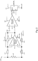
- a plurality of graphs 400 including graphs 410, 420, 430, 440, and 450.
- Graph 410 illustrates the magnitude of a gate voltage 411 applied to the gate of power switch 117.
- Graph 420 illustrates the magnitude of a gate voltage 421 applied to the gate of power switch 119.
- Graph 430 illustrates the magnitude of a voltage across switches 117 and 119 power device 105.
- Graph 440 illustrates the magnitude of current I 131 flowing through resistor 131.
- Graph 450 illustrates the magnitude of voltage V 131 across resistor 131.
- Each graph illustrates electrical characteristics of power system 100 over a time period including time instants t 1 -t 5 .
- switch 119 experiences a failure, causing an increasing gate signal to be applied to the gate of switch 119.
- the gate signal applied to switch 119 closes switch 119 causing power system 100 to begin conducting a short circuit current.
- detection circuit 133 determines a short circuit is occurring based on Voltage V 131 exceeding a voltage threshold.
- gate driver circuits 135 and 137 stop transmitting gate signals to switches 117 and 119 in response to determining the short circuit is occurring. The gate signals decrease until time instant ts when system 130 causes the opening of switches 117 and 119 in response to determining the short circuit is occurring.
- One embodiment is a protection system for a power switch comprising: a resistor coupled in series with a decoupling capacitor; and a detection circuit structured to receive a voltage of the resistor, determine a short circuit is occurring based on the received voltage, and transmit a fault trigger signal in response to determining the short circuit is occurring.
- the protection system comprises a gate driver circuit structured to receive the fault trigger signal and turn off the power switch at a zero current crossing in response to receiving the fault trigger signal.
- the gate driver circuit includes a NOT logic gate structured to receive the fault trigger signal, an AND logic gate coupled to the NOT logic gate, and a soft turn-off circuit structured to receive the fault trigger signal.
- the resistor includes a printed circuit board trace arrangement having an equivalent resistance. In certain forms, the equivalent resistance is between 200 microohms and 10 milliohms.
- the detection circuit comprises: an amplifier structured to receive the resistor voltage; a comparator structured to receive an amplified output from the amplifier and a short circuit voltage threshold; and a signal latch structured to receive a fault detection signal from the comparator and output the fault trigger signal to a gate driver circuit.
- the short circuit voltage threshold corresponds to a first resistor voltage greater than a second resistor voltage generated by a toggling of the power switch.
- the power switch is a wide-bandgap switch, wherein the detection circuit is structured to transmit the fault trigger signal within 50ns of a beginning of the short circuit, and wherein the fault trigger signal is configured to cause a gate driver to turn off the power switch.
- the detection circuit is structured to determine the short circuit is occurring by amplifying the received voltage, comparing the amplified voltage to a short circuit voltage threshold, and determining the amplified voltage is greater than the short circuit voltage threshold, wherein the short circuit voltage threshold is greater than a first resistor voltage generated by a current flowing through the decoupling capacitor during toggling of the power switch.
- the voltage across the resistor is generated by a high frequency current flowing through the decoupling capacitor.
- Another exemplary embodiment is a method for protecting a power switch comprising: receiving, with a detection circuit, a voltage of a resistor coupled in series with a decoupling capacitor; determining, with the detection circuit, a short circuit is occurring based on the received voltage; and transmitting, with the detection circuit, a fault trigger signal in response to determining the short circuit is occurring.
- determining the short circuit is occurring includes: amplifying the received voltage; comparing the amplified voltage to a short circuit voltage threshold; and determining the amplified voltage is greater than the short circuit voltage threshold, wherein the short circuit voltage threshold is based on a first resistor voltage generated by a current flowing through the decoupling capacitor during toggling of the power switch.
- the voltage is generated by a high frequency current flowing through the decoupling capacitor.
Landscapes
- Engineering & Computer Science (AREA)
- Power Engineering (AREA)
- Physics & Mathematics (AREA)
- Nonlinear Science (AREA)
- Emergency Protection Circuit Devices (AREA)
- Power Conversion In General (AREA)
Abstract
Description
- The present disclosure relates generally to power switch protection. Some recently developed types of semiconductor switches fail quickly when conducting short circuit current. For example, some wide-bandgap switches may fail after conducting short circuit current for as little as 600ns. Existing power switch protection systems suffer from a number of shortcomings and disadvantages. There remain unmet needs including increasing protection system responsiveness and reducing protection system power losses. For instance, some conventional protection systems, such as desaturation detection-based systems, do not respond quickly enough to protect wide-bandgap switches from short circuit current. Furthermore, some conventional protection systems monitor a shunt resistor inserted into the load current path, generating constant power losses. In view of these and other shortcomings in the art, there is a significant need for the apparatuses, methods, systems and techniques disclosed herein.
- For the purposes of clearly, concisely and exactly describing non-limiting exemplary embodiments of the disclosure, the manner and process of making and using the same, and to enable the practice, making and use of the same, reference will now be made to certain exemplary embodiments, including those illustrated in the figures, and specific language will be used to describe the same. It shall nevertheless be understood that no limitation of the scope of the present disclosure is thereby created, and that the present disclosure includes and protects such alterations, modifications, and further applications of the exemplary embodiments as would occur to one skilled in the art with the benefit of the present disclosure.
- Exemplary embodiments of the disclosure include systems, methods, techniques and apparatuses for power switch short circuit protection. Further embodiments, forms, objects, features, advantages, aspects and benefits of the disclosure shall become apparent from the following description and drawings.
-
-
Fig. 1 illustrates an exemplary power switch protection system. -
Fig. 2 illustrates an exemplary detection circuit. -
Fig. 3 illustrates an exemplary gate driver circuit. -
Fig. 4 is a plurality of graphs illustrating short circuit protection using the exemplary power switch protection system ofFig. 1 . - With reference to
Fig. 1 , there is illustrated anexemplary power system 100 including a powerswitch protection system 130. It shall be appreciated thatsystem 130 may be implemented in a variety of applications, including bi-level and multi-level power converters, to name but a few examples. It shall be also appreciated that the topology ofsystem 100 is illustrated for the purpose of explanation and is not intended as a limitation of the present disclosure unless otherwise specified. -
Power system 100 is structured to transmit power between anoutput terminal 121 and apower device 105.System 100 may be structured to transmit power unidirectionally frompower device 105 tooutput terminal 121, transmit power unidirectionally fromoutput terminal 121 topower device 105, or transmit power bi-directionally betweenoutput terminal 121 andpower device 105.Output terminal 121 may receive or transmit alternating current (AC) or direct current (DC) power.Power device 105 is structured to transmit or receive DC power. -
Power system 100 includes a DC bus including aDC bus rail 101 and aDC bus rail 103. Four legs are coupled across the DC bus. Between the first leg and the second leg, the DC bus has aparasitic inductance 111. Between the second leg and third leg, the DC bus has aparasitic inductance 113. Between the third leg and the fourth leg, the DC bus has aparasitic inductance 115. - The first leg includes a
power switch 117 and apower switch 119 structured to convert or transmit power betweenoutput terminal 121 andpower device 105. For example,power switch 117 andpower switch 119 may convert AC power received fromoutput terminal 121 into DC power, or convert DC power received from the DC bus into AC power.Power switch 117 is coupled betweenDC bus rail 101 andoutput terminal 121, andpower switch 119 is coupled betweenDC bus rail 103 andoutput terminal 121. Eachpower switch - The second leg includes a
decoupling capacitor 109 and aresistor 131 coupled in series betweenDC bus rail 101 andDC bus rail 103.Decoupling capacitor 109 is structured to reduce electric noise generated by operation ofpower switches decoupling capacitor 109 may be a ceramic capacitor or a film capacitor. In certain embodiments, the capacitance of decoupling capacitor may be between 100nF to 1uF, or may be 10-100 times the output capacitance ofpower switches -
Resistor 131 may include an external resistor or an equivalent resistor. For example,resistor 131 may include an external resistor having a resistance or a printed circuit board trace arrangement having an equivalent resistance.Resistor 131 is structured to have a small resistance R131. For example, the resistance or equivalent resistance ofresistor 131 may be between 200 microohms and 10 milliohms, or between 200 microohms and 800 microohms, to give but a few examples. - The components of the first leg and the second leg form a
high frequency loop 123 such that only transient current, such as noise from the operation of the power switches, flow through the second leg, includingresistor 131. Therefore, power losses fromresistor 131 of the second leg are negligible compared to placing a resistor with the same resistance in the current path of load current I105. By placingresistor 131 inhigh frequency loop 123,resistor 131 induces an inductance L131. In certain embodiments,resistor 131 is located within 10mm ofpower switch 119. - The third leg includes a
DC link capacitor 107 coupled betweenDC bus rail 101 andDC bus rail 103. In certain embodiments,DC link capacitor 107 includes a capacitance greater than the capacitance of the decoupling capacitor. For example, the capacitance ofDC link capacitor 107 may be 100 times greater than the capacitance of decouplingcapacitor 109.DC link capacitor 107 is also placed farther away fromswitches decoupling capacitor 109. For example, decoupling capacitor may be placed less than 10mm frompower switches - The fourth leg includes a
power device 105 coupled betweenDC bus rail 101 andDC bus rail 103. In the illustrated embodiment,power device 105 is an energy storage device structured to receive power from the DC bus, store energy, and provide power to the DC bus.Power device 105 may also be a power generation device, or another type of device structured to receive or transmit DC power. - Power
switch protection system 130 is structured to protectpower system 100 from short circuits occurring withinpower system 100. For example,system 130 may protectsystem 100 from phase-leg short circuits or phase-to-phase short circuits. Powerswitch protection system 130 includesresistor 131, adetection circuit 133, andgate driver circuits -
Detection circuit 133 is structured to measure a voltage V131 acrossresistor 131. When current flows throughhigh frequency loop 123, the current causes voltage V131 acrossresistor 131. During normal operation, transient current generated by power switch toggling flows throughresistor 131 due to decouplingcapacitor 109 absorbing changes in voltage caused by the toggling. While the power switch toggling may cause voltage oscillation in the DC bus,detection circuit 133 determines the voltage V131 acrossresistor 131 remains below a short circuit threshold. Once a short circuit occurs, short circuit current flows throughhigh frequency loop 123, causingdetection circuit 133 to determine voltage V131 acrossresistor 131 exceeds the short circuit threshold. - The short circuit threshold is a voltage greater than the voltage across
resistor 131 generated by power switch toggling. In certain embodiments, the short circuit threshold is 3-5 times the peak nominal voltage across the resistor caused by power switch toggling. In certain embodiments,detection circuit 133 determines a short circuit is occurring within 50ns of the beginning of the short circuit. -
Gate driver circuit 135 is structured to operatepower switch 119 andgate driver circuit 137 is structured to operatepower switch 117. As described in more detail below with respect togate driver circuit 300 ofFig. 3 ,gate driver circuits detection circuit 133 and, in response to receiving a fault trigger signal indicating a short circuit is occurring, turn offpower switches power system 100 may also be present in the other components disclosed herein. - With reference to
Fig. 2 , there is a circuit diagram illustrating anexemplary detection circuit 200, such asdetection circuit 133 ofpower system 100 inFig. 1 .Circuit 200 is coupled toresistor 201 and structured to receive an electrical characteristic ofresistor 201, determine whether a short circuit fault is occurring in a powersystem incorporating resistor 201 based on the received electrical characteristic, and output a fault trigger signal in response to determining a short circuit fault is occurring. -
Circuit 200 includes a high bandwidthdifferential amplifier 215, ahigh speed comparator 227, and asignal latch 229, each of which are coupled to a lowvoltage power source 221 and aground reference point 223. Lowvoltage power source 221 may output a voltage less than 10 V, to name but one example, and is structured to provide power toamplifier 215,comparator 227, andlatch 229. In certain embodiments, one or more ofamplifier 215,comparator 227, and latch 229 are coupled to different low voltage power sources. -
Amplifier 215 includes a positive input terminal and a negative input terminal each coupled toresistor 201 such thatamplifier 215 is coupled in parallel withresistor 201.Resistor 201 is coupled to the negative input terminal ofamplifier 215 by way of aresistor 211 and coupled to the positive input terminal ofamplifier 215 by way ofresistor 213. The positive input terminal ofamplifier 215 is also coupled toground reference point 223 by way ofresistor 214. The negative input terminal ofamplifier 215 is also coupled to an output terminal ofamplifier 215 by way of aresistor 219 and acapacitor 217 coupled in parallel between the negative input terminal and the output terminal. In certain embodiments, the resistances of theresistors -
Amplifier 215 is structured to receive an input signal at the negative and positive input terminals, the input signal corresponding to an electrical characteristic ofresistor 201, such as the voltage acrossresistor 201.Amplifier 215 is structured to amplify the magnitude of the input signal, generating an amplified signal which is output at the output terminal ofamplifier 215. By amplifying the input signal,amplifier 215 increases the accuracy ofdetection circuit 200. - It is important to note that
decoupling capacitor 109, resistance R131, inductance L131, andparasitic inductance 111 ofFig. 1 form an RLC circuit. Therefore, thehigh frequency loop 123 is structured to filter noise having a frequency greater than 1 MHz fromamplifier 215. For example, high frequency noise may be caused by the switching ofswitches resistor 219 andcapacitor 217 form a low pass filter structured to further filter high frequency noise. -
Comparator 227 is coupled to the output terminal ofamplifier 215 and structured to receive the amplified signal fromamplifier 215 at a positive input terminal ofcomparator 227.Comparator 227 is also coupled to apower source 226 at a negative input terminal ofcomparator 227 and structured to receive a voltage frompower source 226 corresponding to a threshold voltage. The threshold voltage corresponds to a minimum voltage acrossresistor 201 which indicates a short circuit. -
Comparator 227 is structured to compare the received amplified signal and the received threshold voltage and output a fault detection signal based on the comparison between the received amplified signal and the received threshold voltage. During normal operation of the monitored power system, the received amplified signal is smaller than the received threshold voltage, andcomparator 227 is structured to output a low fault detection signal indicating no short circuit is detected. During a short circuit, the received amplified signal exceeds the received threshold voltage, andcomparator 227 is structured to output a high fault detection signal indicating a short circuit fault has been detected. - In the illustrated
circuit 200,latch 229 is a D flip-flop. In other embodiments, latch 229 may be another type of signal latch.Latch 229 includes a clock terminal CLK, an input terminal D, and an output terminal Q. Clock terminal CLK is coupled to the output terminal ofcomparator 227 and is structured to receive the fault detection signal fromcomparator 227. Input terminal D is structured to receive a constant high fault detection signal from a power source. Output terminal Q is structured to output a fault trigger signal. Whenlatch 229 receives a high fault detection signal fromcomparator 227 indicating a short circuit fault has been detected, latch 229 outputs a fault trigger signal configured to cause gate driver circuits to respond to a detected short circuit fault. - In certain embodiments,
detection circuit 200 is structured to detect a short circuit within 100ns of the beginning of the short circuit beginning. For example,detection circuit 200 may be structured to detect a short circuit within 50ns of the beginning of the short circuit. It shall be appreciated that any or all of the foregoing features ofdetection circuit 200 may also be present in the other detection circuits disclosed herein, such asdetection circuit 133 ofFig. 1 . - With reference to
Fig. 3 , there is a circuit diagram illustrating an exemplarygate driver circuit 300 coupled to a wide-bandgap switch 307.Gate driver circuit 300 is structured to turn on and turn offswitch 307 based on a gate signal and a fault trigger signal.Switch 307 includes agate terminal 301, adrain terminal 305, and asource terminal 303.Circuit 300 is coupled togate terminal 301 andsource terminal 303.Gate driver circuit 300 includes a digital isolator 306, an ANDlogic gate 319, aNOT logic gate 321, a gate driver integratedcircuit 323, and a soft turn-off circuit 333. - Digital isolator 306 includes a primary side and a secondary side. A
primary voltage source 311, aground 315, and agate signal source 309 are coupled to the primary side of digital isolator 306. Asecondary voltage source 313, aground reference 317, and anoutput terminal 314 are coupled to the secondary side of digital isolator 306. Digital isolator 306 is structured to receive a gate signal fromgate signal source 309 by way of aninput terminal 312 and output an isolated gate signal corresponding to the received gate signal fromoutput terminal 314. -
NOT logic gate 321 is structured to receive the fault trigger signal from an exemplary detection circuit, such asdetection circuit 200 ofFig. 2 , invert the received signal, and output the inverted signal. ANDlogic gate 319 is coupled tovoltage source 313,ground reference 317,output terminal 314, andNOT logic gate 321. ANDlogic gate 319 is structured to receive the inverted signal fromNOT logic gate 321 and the isolated gate signal fromoutput terminal 314, and output a signal to gate driver integratedcircuit 323 based on the received signals. For example, if the received isolated gate signal is a high value, indicatingswitch 307 should be turned on, and the fault trigger signal is a low value, indicating there is no short circuit,logic gate 319 will output asignal indicating switch 307 should be turned on. In another example, if the received isolated gate signals a high value, but the fault trigger signal is also a high value, indicating there is a short circuit,logic gate 319 will output asignal indicating switch 307 should be turned off or remain off. - Gate driver integrated
circuit 323 is coupled to apower source 329,ground reference 317, and ANDlogic gate 319. Gate driver integratedcircuit 323 includes asignal processor 327, aswitch 325, and anotherswitch 328. Gate driver integratedcircuit 323 is structured to receive the signal output bylogic gate 319, and generate an outputsignal using switches gate terminal 301 ofswitch 307 by way ofgate resistor 331. - Soft turn-
off circuit 333 is coupled betweengate terminal 301 andsource terminal 303. Soft turn-off circuit 333 is structured to receive a fault trigger signal indicating a short circuit and, in response, modify the signal output by gate driver integratedcircuit 323 so thatswitch 307 is turned off at a zero current crossing. In certain embodiments, soft turn-off circuit 333 is structured to increase a gate resistance in order to reduce voltage and current oscillations in the gate signal. It shall be appreciated that any or all of the foregoing features ofgate driver circuit 300 may also be present in the other gate driver circuits disclosed herein, such asgate driver circuits Fig. 1 . - With reference to
Fig. 4 , there is illustrated a plurality ofgraphs 400 includinggraphs Graph 410 illustrates the magnitude of agate voltage 411 applied to the gate ofpower switch 117.Graph 420 illustrates the magnitude of agate voltage 421 applied to the gate ofpower switch 119.Graph 430 illustrates the magnitude of a voltage acrossswitches power device 105.Graph 440 illustrates the magnitude of current I131 flowing throughresistor 131.Graph 450 illustrates the magnitude of voltage V131 acrossresistor 131. - Each graph illustrates electrical characteristics of
power system 100 over a time period including time instants t1-t5. At time instant t1, switch 119 experiences a failure, causing an increasing gate signal to be applied to the gate ofswitch 119. At time instant t2, the gate signal applied to switch 119 closes switch 119 causingpower system 100 to begin conducting a short circuit current. At time instant t3,detection circuit 133 determines a short circuit is occurring based on Voltage V131 exceeding a voltage threshold. At time instant t4,gate driver circuits switches system 130 causes the opening ofswitches - Further written description of a number of exemplary embodiments shall now be provided. One embodiment is a protection system for a power switch comprising: a resistor coupled in series with a decoupling capacitor; and a detection circuit structured to receive a voltage of the resistor, determine a short circuit is occurring based on the received voltage, and transmit a fault trigger signal in response to determining the short circuit is occurring.
- In certain forms of the foregoing protection system, the protection system comprises a gate driver circuit structured to receive the fault trigger signal and turn off the power switch at a zero current crossing in response to receiving the fault trigger signal. In certain forms, the gate driver circuit includes a NOT logic gate structured to receive the fault trigger signal, an AND logic gate coupled to the NOT logic gate, and a soft turn-off circuit structured to receive the fault trigger signal. In certain forms, the resistor includes a printed circuit board trace arrangement having an equivalent resistance. In certain forms, the equivalent resistance is between 200 microohms and 10 milliohms. In certain forms, the detection circuit comprises: an amplifier structured to receive the resistor voltage; a comparator structured to receive an amplified output from the amplifier and a short circuit voltage threshold; and a signal latch structured to receive a fault detection signal from the comparator and output the fault trigger signal to a gate driver circuit. In certain forms, the short circuit voltage threshold corresponds to a first resistor voltage greater than a second resistor voltage generated by a toggling of the power switch. In certain forms, the power switch is a wide-bandgap switch, wherein the detection circuit is structured to transmit the fault trigger signal within 50ns of a beginning of the short circuit, and wherein the fault trigger signal is configured to cause a gate driver to turn off the power switch. In certain forms, the detection circuit is structured to determine the short circuit is occurring by amplifying the received voltage, comparing the amplified voltage to a short circuit voltage threshold, and determining the amplified voltage is greater than the short circuit voltage threshold, wherein the short circuit voltage threshold is greater than a first resistor voltage generated by a current flowing through the decoupling capacitor during toggling of the power switch. In certain forms, the voltage across the resistor is generated by a high frequency current flowing through the decoupling capacitor.
- Another exemplary embodiment is a method for protecting a power switch comprising: receiving, with a detection circuit, a voltage of a resistor coupled in series with a decoupling capacitor; determining, with the detection circuit, a short circuit is occurring based on the received voltage; and transmitting, with the detection circuit, a fault trigger signal in response to determining the short circuit is occurring.
- In certain forms of the foregoing method, the method comprises receiving, with a gate driver circuit, the fault trigger signal; and turning off, with the gate driver circuit, the power switch at a zero current crossing in response to receiving the fault trigger signal. In certain forms, receiving the fault trigger signal includes receiving the fault trigger signal with a NOT logic gate of the gate driver circuit and receiving the fault trigger signal with a soft turn-off circuit of the gate driver circuit, and wherein the method comprises receiving, with an AND logic gate, an inverted signal of the fault trigger signal from the NOT logic gate. In certain forms, the resistor includes a printed circuit board trace arrangement having an equivalent resistance. In certain forms, the equivalent resistance is between 200 microohms and 10 milliohms. In certain forms, the method comprises receiving, with a comparator of the detection circuit, an amplified output from an amplifier and a short circuit voltage threshold; receiving, with a signal latch, a fault detection signal from the comparator; and outputting, with the signal latch, the fault trigger signal to a gate driver circuit. In certain forms, the short circuit voltage threshold corresponds to a first resistor voltage greater than a second resistor voltage generated by a toggling of the power switch. In certain forms, the power switch is a wide-bandgap switch, wherein transmitting, with the detection circuit, the fault trigger signal occurs within 50ns of a beginning of the short circuit, and wherein the fault trigger signal is configured to cause a gate driver to turn off the power switch. In certain forms, determining the short circuit is occurring includes: amplifying the received voltage; comparing the amplified voltage to a short circuit voltage threshold; and determining the amplified voltage is greater than the short circuit voltage threshold, wherein the short circuit voltage threshold is based on a first resistor voltage generated by a current flowing through the decoupling capacitor during toggling of the power switch. In certain forms, the voltage is generated by a high frequency current flowing through the decoupling capacitor.
- While the present disclosure has been illustrated and described in detail in the drawings and foregoing description, the same is to be considered as illustrative and not restrictive in character, it being understood that only certain exemplary embodiments have been shown and described, and that all changes and modifications that come within the spirit of the present disclosure are desired to be protected. It should be understood that while the use of words such as "preferable," "preferably," "preferred" or "more preferred" utilized in the description above indicate that the feature so described may be more desirable, it nonetheless may not be necessary, and embodiments lacking the same may be contemplated as within the scope of the present disclosure, the scope being defined by the claims that follow. In reading the claims, it is intended that when words such as "a," "an," "at least one," or "at least one portion" are used there is no intention to limit the claim to only one item unless specifically stated to the contrary in the claim. The term "of' may connote an association with, or a connection to, another item, as well as a belonging to, or a connection with, the other item as informed by the context in which it is used. The terms "coupled to," "coupled with" and the like include indirect connection and coupling, and further include but do not require a direct coupling or connection unless expressly indicated to the contrary. When the language "at least a portion" and/or "a portion" is used, the item can include a portion and/or the entire item unless specifically stated to the contrary.
Claims (15)
- A protection system for a power switch comprising:a resistor coupled in series with a decoupling capacitor; anda detection circuit structured to receive a voltage of the resistor, determine a short circuit is occurring based on the received voltage, and transmit a fault trigger signal in response to determining the short circuit is occurring.
- The protection system of claim 1, comprising:a gate driver circuit structured to receive the fault trigger signal and turn off the power switch at a zero current crossing in response to receiving the fault trigger signal.
- The protection system of claim 2, wherein the gate driver circuit includes a NOT logic gate structured to receive the fault trigger signal, an AND logic gate coupled to the NOT logic gate, and a soft turn-off circuit structured to receive the fault trigger signal.
- The protection system of claim 1, wherein the resistor includes a printed circuit board trace arrangement having an equivalent resistance, preferably, wherein the equivalent resistance is between 200 microohms and 10 milliohms.
- The protection system of claim 1, wherein the detection circuit comprises:an amplifier structured to receive the resistor voltage;a comparator structured to receive an amplified output from the amplifier and a short circuit voltage threshold, preferably wherein the short circuit voltage threshold corresponds to a first resistor voltage greater than a second resistor voltage generated by a toggling of the power switch; anda signal latch structured to receive a fault detection signal from the comparator and output the fault trigger signal to a gate driver circuit.
- The protection system of claim 1, wherein the power switch is a wide-bandgap switch, wherein the detection circuit is structured to transmit the fault trigger signal within 50ns of a beginning of the short circuit, and wherein the fault trigger signal is configured to cause a gate driver to turn off the power switch.
- The protection system of claim 1, wherein the detection circuit is structured to determine the short circuit is occurring by amplifying the received voltage, comparing the amplified voltage to a short circuit voltage threshold, and determining the amplified voltage is greater than the short circuit voltage threshold, wherein the short circuit voltage threshold is greater than a first resistor voltage generated by a current flowing through the decoupling capacitor during toggling of the power switch.
- The protection system of claim 1, wherein the voltage across the resistor is generated by a high frequency current flowing through the decoupling capacitor.
- A method for protecting a power switch comprising:receiving, with a detection circuit, a voltage of a resistor coupled in series with a decoupling capacitor;determining, with the detection circuit, a short circuit is occurring based on the received voltage; andtransmitting, with the detection circuit, a fault trigger signal in response to determining the short circuit is occurring.
- The method of claim 9 comprising:receiving, with a gate driver circuit, the fault trigger signal; andturning off, with the gate driver circuit, the power switch at a zero current crossing in response to receiving the fault trigger signal.
- The method of claim 10, wherein receiving the fault trigger signal includes receiving the fault trigger signal with a NOT logic gate of the gate driver circuit and receiving the fault trigger signal with a soft turn-off circuit of the gate driver circuit, and wherein the method comprises receiving, with an AND logic gate, an inverted signal of the fault trigger signal from the NOT logic gate.
- The method of claim 9, wherein the resistor includes a printed circuit board trace arrangement having an equivalent resistance; or
wherein the equivalent resistance is between 200 microohms and 10 milliohms. - The method of claim 9, comprising:receiving, with a comparator of the detection circuit, an amplified output from an amplifier and a short circuit voltage threshold;receiving, with a signal latch, a fault detection signal from the comparator; andoutputting, with the signal latch, the fault trigger signal to a gate driver circuit.
- The method of claim 13, wherein the short circuit voltage threshold corresponds to a first resistor voltage greater than a second resistor voltage generated by a toggling of the power switch.
- The method of claim 9, wherein the power switch is a wide-bandgap switch, wherein transmitting, with the detection circuit, the fault trigger signal occurs within 50ns of a beginning of the short circuit, and wherein the fault trigger signal is configured to cause a gate driver to turn off the power switch; or
wherein determining the short circuit is occurring includes:amplifying the received voltage;comparing the amplified voltage to a short circuit voltage threshold; anddetermining the amplified voltage is greater than the short circuit voltage threshold,wherein the short circuit voltage threshold is based on a first resistor voltage generated by a current flowing through the decoupling capacitor during toggling of the power switch; orwherein the voltage is generated by a high frequency current flowing through the decoupling capacitor.
Applications Claiming Priority (1)
| Application Number | Priority Date | Filing Date | Title |
|---|---|---|---|
| US16/912,775 US20210409016A1 (en) | 2020-06-26 | 2020-06-26 | Power switch short circuit protection |
Publications (1)
| Publication Number | Publication Date |
|---|---|
| EP3930192A1 true EP3930192A1 (en) | 2021-12-29 |
Family
ID=76502685
Family Applications (1)
| Application Number | Title | Priority Date | Filing Date |
|---|---|---|---|
| EP21181754.9A Withdrawn EP3930192A1 (en) | 2020-06-26 | 2021-06-25 | Power switch short circuit protection |
Country Status (3)
| Country | Link |
|---|---|
| US (1) | US20210409016A1 (en) |
| EP (1) | EP3930192A1 (en) |
| CN (1) | CN113852048A (en) |
Families Citing this family (1)
| Publication number | Priority date | Publication date | Assignee | Title |
|---|---|---|---|---|
| EP4287510A1 (en) * | 2022-06-02 | 2023-12-06 | Airbus S.A.S. | Overcurrent protection circuit for fast switching semiconductors, and method of protecting fast switching semiconductors from overcurrents |
Citations (2)
| Publication number | Priority date | Publication date | Assignee | Title |
|---|---|---|---|---|
| JP2002291241A (en) * | 2001-03-23 | 2002-10-04 | Densei Lambda Kk | Switching power supply |
| US20110210713A1 (en) * | 2007-12-20 | 2011-09-01 | Shun Kazama | Power conversion apparatus and control method for power conversion apparatus |
Family Cites Families (11)
| Publication number | Priority date | Publication date | Assignee | Title |
|---|---|---|---|---|
| DE19619120A1 (en) * | 1996-05-11 | 1997-11-13 | Telefunken Microelectron | Power FET switching and short circuit recognition module |
| US7593200B2 (en) * | 2006-08-15 | 2009-09-22 | International Rectifier Corporation | Buck converter fault detection method |
| ITMI20071846A1 (en) * | 2007-09-25 | 2009-03-26 | St Microelectronics Srl | "PROTECTION DEVICE FOR ELECTRONIC CIRCUITS AGAINST MALFUNCTIONS" |
| JP2009303317A (en) * | 2008-06-11 | 2009-12-24 | Ricoh Co Ltd | Reference voltage generating circuit and dc-dc converter with that reference voltage generating circuit |
| US9955272B2 (en) * | 2015-06-04 | 2018-04-24 | Cirrus Logic, Inc. | Audio connector and circuitry |
| US10720846B2 (en) * | 2017-01-05 | 2020-07-21 | Dialog Semiconductor Inc. | Sense resistor short detection for switching power converters |
| US10712210B2 (en) * | 2017-12-29 | 2020-07-14 | Nxp Usa, Inc. | Self-referenced, high-accuracy temperature sensors |
| CN108508342B (en) * | 2018-05-28 | 2020-07-17 | 中国科学院上海微系统与信息技术研究所 | IGBT short circuit overcurrent detection circuit |
| US10992293B2 (en) * | 2018-09-20 | 2021-04-27 | Texas Instruments Incorporated | Device with isolation barrier and fault detection |
| CN109888739B (en) * | 2019-01-30 | 2023-12-15 | 上海拓为汽车技术有限公司 | MOSFET short-circuit protection circuit for drive axle |
| CN210806715U (en) * | 2019-07-24 | 2020-06-19 | 江苏赣锋动力科技有限公司 | Short-circuit protection circuit based on operational amplifier and triode |
-
2020
- 2020-06-26 US US16/912,775 patent/US20210409016A1/en not_active Abandoned
-
2021
- 2021-06-25 EP EP21181754.9A patent/EP3930192A1/en not_active Withdrawn
- 2021-06-28 CN CN202110719080.6A patent/CN113852048A/en active Pending
Patent Citations (2)
| Publication number | Priority date | Publication date | Assignee | Title |
|---|---|---|---|---|
| JP2002291241A (en) * | 2001-03-23 | 2002-10-04 | Densei Lambda Kk | Switching power supply |
| US20110210713A1 (en) * | 2007-12-20 | 2011-09-01 | Shun Kazama | Power conversion apparatus and control method for power conversion apparatus |
Also Published As
| Publication number | Publication date |
|---|---|
| CN113852048A (en) | 2021-12-28 |
| US20210409016A1 (en) | 2021-12-30 |
Similar Documents
| Publication | Publication Date | Title |
|---|---|---|
| US11683030B2 (en) | Protecting semiconductor switches in switched mode power converters | |
| US7463079B2 (en) | Short circuit protection by gate voltage sensing | |
| CN112838746A (en) | Gate driver with integrated miller clamp | |
| JP2007259533A (en) | Protective circuit for semiconductor element | |
| KR20080045927A (en) | System for fault protection in igbt | |
| Jones et al. | A fast overcurrent protection scheme for GaN GITs | |
| US10181847B2 (en) | Ring amplitude measurement and mitigation | |
| US10917081B1 (en) | Adjustable soft shutdown and current booster for gate driver | |
| CN113014234B (en) | Overcurrent protection and floating level shift circuit applied to half-bridge high-voltage drive | |
| Acuna et al. | Very fast short circuit protection for gallium-nitride power transistors based on printed circuit board integrated current sensor | |
| EP3930192A1 (en) | Power switch short circuit protection | |
| US11601054B2 (en) | Power semiconductor device protection circuit and power module | |
| Li et al. | An ultra-fast short circuit protection solution for E-mode GaN HEMTs | |
| Alemdar et al. | PCB layout based short-circuit protection scheme for GaN HEMTs | |
| US20200280308A1 (en) | Short-circuit protection of power semiconductor device by sensing current injection from drain to gate | |
| Lyu et al. | A reliable ultra-fast three step short circuit protection method for E-mode GaN HEMTs | |
| US11695405B2 (en) | Short circuit protection for semiconductor switches | |
| US6396674B1 (en) | System and method for monitoring the operation of a power converter | |
| KR20230173307A (en) | Threshold voltage level conversion type Short circuit protection circuit for power switch | |
| US8575974B2 (en) | Method and control circuit for controlling a power semiconductor component | |
| US11171559B2 (en) | Overcurrent protection detector with dynamic threshold for power conversion switch | |
| CN113474982B (en) | System and method for protecting power semiconductors of a half-bridge converter | |
| Liu et al. | A Comprehensive Short-Circuit Protection Scheme for Series-Connected SiC MOSFETs | |
| US20240019501A1 (en) | Method and apparatus for fast short circuit detection of a short circuit at a gate-controlled power switch | |
| US20240072530A1 (en) | Short-circuit detector for electronic fuse circuit |
Legal Events
| Date | Code | Title | Description |
|---|---|---|---|
| PUAI | Public reference made under article 153(3) epc to a published international application that has entered the european phase |
Free format text: ORIGINAL CODE: 0009012 |
|
| STAA | Information on the status of an ep patent application or granted ep patent |
Free format text: STATUS: THE APPLICATION HAS BEEN PUBLISHED |
|
| AK | Designated contracting states |
Kind code of ref document: A1 Designated state(s): AL AT BE BG CH CY CZ DE DK EE ES FI FR GB GR HR HU IE IS IT LI LT LU LV MC MK MT NL NO PL PT RO RS SE SI SK SM TR |
|
| B565 | Issuance of search results under rule 164(2) epc |
Effective date: 20211112 |
|
| STAA | Information on the status of an ep patent application or granted ep patent |
Free format text: STATUS: REQUEST FOR EXAMINATION WAS MADE |
|
| 17P | Request for examination filed |
Effective date: 20220629 |
|
| RBV | Designated contracting states (corrected) |
Designated state(s): AL AT BE BG CH CY CZ DE DK EE ES FI FR GB GR HR HU IE IS IT LI LT LU LV MC MK MT NL NO PL PT RO RS SE SI SK SM TR |
|
| STAA | Information on the status of an ep patent application or granted ep patent |
Free format text: STATUS: THE APPLICATION IS DEEMED TO BE WITHDRAWN |
|
| 18D | Application deemed to be withdrawn |
Effective date: 20240103 |