EP3930018A1 - Organic semiconductor device, method for manufacturing organic semiconductor single-crystal film, and method for manufacturing organic semiconductor device - Google Patents
Organic semiconductor device, method for manufacturing organic semiconductor single-crystal film, and method for manufacturing organic semiconductor device Download PDFInfo
- Publication number
- EP3930018A1 EP3930018A1 EP20759235.3A EP20759235A EP3930018A1 EP 3930018 A1 EP3930018 A1 EP 3930018A1 EP 20759235 A EP20759235 A EP 20759235A EP 3930018 A1 EP3930018 A1 EP 3930018A1
- Authority
- EP
- European Patent Office
- Prior art keywords
- organic semiconductor
- single crystal
- crystal film
- substrate
- semiconductor single
- Prior art date
- Legal status (The legal status is an assumption and is not a legal conclusion. Google has not performed a legal analysis and makes no representation as to the accuracy of the status listed.)
- Pending
Links
Images





Classifications
-
- H—ELECTRICITY
- H10—SEMICONDUCTOR DEVICES; ELECTRIC SOLID-STATE DEVICES NOT OTHERWISE PROVIDED FOR
- H10K—ORGANIC ELECTRIC SOLID-STATE DEVICES
- H10K10/00—Organic devices specially adapted for rectifying, amplifying, oscillating or switching; Organic capacitors or resistors having potential barriers
- H10K10/40—Organic transistors
- H10K10/46—Field-effect transistors, e.g. organic thin-film transistors [OTFT]
-
- H—ELECTRICITY
- H10—SEMICONDUCTOR DEVICES; ELECTRIC SOLID-STATE DEVICES NOT OTHERWISE PROVIDED FOR
- H10K—ORGANIC ELECTRIC SOLID-STATE DEVICES
- H10K10/00—Organic devices specially adapted for rectifying, amplifying, oscillating or switching; Organic capacitors or resistors having potential barriers
-
- H—ELECTRICITY
- H10—SEMICONDUCTOR DEVICES; ELECTRIC SOLID-STATE DEVICES NOT OTHERWISE PROVIDED FOR
- H10K—ORGANIC ELECTRIC SOLID-STATE DEVICES
- H10K71/00—Manufacture or treatment specially adapted for the organic devices covered by this subclass
- H10K71/10—Deposition of organic active material
- H10K71/12—Deposition of organic active material using liquid deposition, e.g. spin coating
-
- H—ELECTRICITY
- H10—SEMICONDUCTOR DEVICES; ELECTRIC SOLID-STATE DEVICES NOT OTHERWISE PROVIDED FOR
- H10K—ORGANIC ELECTRIC SOLID-STATE DEVICES
- H10K71/00—Manufacture or treatment specially adapted for the organic devices covered by this subclass
- H10K71/80—Manufacture or treatment specially adapted for the organic devices covered by this subclass using temporary substrates
-
- H—ELECTRICITY
- H10—SEMICONDUCTOR DEVICES; ELECTRIC SOLID-STATE DEVICES NOT OTHERWISE PROVIDED FOR
- H10K—ORGANIC ELECTRIC SOLID-STATE DEVICES
- H10K10/00—Organic devices specially adapted for rectifying, amplifying, oscillating or switching; Organic capacitors or resistors having potential barriers
- H10K10/40—Organic transistors
- H10K10/46—Field-effect transistors, e.g. organic thin-film transistors [OTFT]
- H10K10/462—Insulated gate field-effect transistors [IGFETs]
- H10K10/484—Insulated gate field-effect transistors [IGFETs] characterised by the channel regions
-
- H—ELECTRICITY
- H10—SEMICONDUCTOR DEVICES; ELECTRIC SOLID-STATE DEVICES NOT OTHERWISE PROVIDED FOR
- H10K—ORGANIC ELECTRIC SOLID-STATE DEVICES
- H10K85/00—Organic materials used in the body or electrodes of devices covered by this subclass
- H10K85/60—Organic compounds having low molecular weight
- H10K85/649—Aromatic compounds comprising a hetero atom
- H10K85/657—Polycyclic condensed heteroaromatic hydrocarbons
- H10K85/6576—Polycyclic condensed heteroaromatic hydrocarbons comprising only sulfur in the heteroaromatic polycondensed ring system, e.g. benzothiophene
-
- H—ELECTRICITY
- H10—SEMICONDUCTOR DEVICES; ELECTRIC SOLID-STATE DEVICES NOT OTHERWISE PROVIDED FOR
- H10K—ORGANIC ELECTRIC SOLID-STATE DEVICES
- H10K85/00—Organic materials used in the body or electrodes of devices covered by this subclass
- H10K85/701—Langmuir Blodgett films
Definitions
- an organic semiconductor film could not be formed on a hydrophobic substrate, such as a fluorine-based polymer insulating film.
- the organic semiconductor device of the present disclosure at least a part of the surface of the substrate in contact with the organic semiconductor single crystal film, preferably the entire surface of the substrate in contact with the organic semiconductor single crystal film, more preferably the entire substrate exhibits hydrophobicity in the above preferable range, whereby when a device is manufactured using an organic semiconductor single crystal film disposed on the hydrophobic substrate, moisture (adsorbed molecules) that can be attached to the substrate can be reduced or eliminated, and a device having favorable characteristics without influence of moisture can be manufactured.
- hydrophobic substrate examples include parylene (contact angle: about 80 to 90 degrees), CYTOP (registered trademark) (contact angle: 110 degrees) which is a fluorine-based polymer, and the like.
- the solvent soluble means substantially dissolving, decomposing, or swelling in an organic solvent, and means substantially dissolving, decomposing, or swelling with respect to an organic solvent conventionally used in a coating method, for example, toluene, dichlorobenzene, or the like.
- At least a part of the surface of the substrate in contact with the organic semiconductor single crystal film preferably the entire surface of the substrate in contact with the organic semiconductor single crystal film, more preferably the entire substrate may be non-heat resistant. Therefore, at least a part of the surface of the substrate in contact with the organic semiconductor single crystal film, preferably the entire surface of the substrate in contact with the organic semiconductor single crystal film, more preferably the entire substrate, may be a substrate having an electrode film of Au or the like modified with a self-assembled monolayer (SAM: self-assembled monolayer), such as pentafluorobenzene thiol (PFBT), for example.
- SAM self-assembled monolayer
- PFBT pentafluorobenzene thiol
- the organic semiconductor single crystal film can be disposed on such a modifying material having low heat resistance, such as PFBT or the like.
- each of R3, R4, R5 and R6 is independently a hydrogen atom or an alkyl group having 1 to 14 carbon atoms.
- the alkyl group may comprise a heteroatom (typically selected from an oxygen atom and a sulfur atom), and the hydrogen atom in the alkyl group may be substituted with a substituent, such as a halogen atom.
- an organic semiconductor single crystal film of the present disclosure it is possible to provide an organic semiconductor single crystal film that can be disposed on a desired substrate and has a thickness thinner than that of a conventional film.
- the first substrate is a hydrophilic substrate having a contact angle of water of preferably 20 degrees or less, more preferably 10 degrees or less.
- the first substrate is non-water-soluble and can be, for example, mica or glass. Since the first substrate is non-water-soluble, when water is applied to the interface between the first substrate and the organic semiconductor single crystal film, components of the first substrate are not eluted and do not adhere to or react with the organic semiconductor single crystal film, so that a high-purity organic semiconductor single crystal film can be obtained. Further, when applying water to the interface between the first substrate and the organic semiconductor single crystal film, in order to maintain the shape of the first substrate without collapsing, it is possible to separate the organic semiconductor single crystal film from the first substrate without distorting the shape of the organic semiconductor single crystal film.
- the non-water-soluble means that it does not substantially dissolve, decompose, or swell in water.
- the glass is preferably subjected to a hydrophilic treatment on the surface by UV-ozone treatment or a hydrophilic
- the method of applying water to the interface between the first substrate and the organic semiconductor single crystal film preferably comprises immersing the first substrate on which the organic semiconductor single crystal film is formed in water.
- the organic semiconductor single crystal film is separated from the first substrate in water, and an organic semiconductor single crystal film which is self-standing in water can be obtained.
- the self-standing organic semiconductor single crystal film can be disposed on any substrate, such as a hydrophobic substrate, a solvent-soluble substrate, a non-heat-resistant substrate, or a substrate having a concave portion, a convex portion, an uneven portion, or an electrode, or a mesh-shaped or grid-shaped substrate in the organic semiconductor device described above.
- the disposing the organic semiconductor single crystal film on the second substrate preferably comprises immersing the first substrate having the organic semiconductor single crystal film formed thereon in water, separating the organic semiconductor single crystal film from the first substrate in water to obtain a self-standing organic semiconductor single crystal film, and disposing the organic semiconductor single crystal film on the second substrate in water.
- the disposing the organic semiconductor single crystal film on the second substrate in water, by disposing a free-standing organic semiconductor single crystal film on the second substrate, it is possible to easily transfer the organic semiconductor single crystal film from the first substrate to the second substrate.
- FIG. 3 shows an electron diffraction pattern obtained by transmission electron microscopy (TEM) observation of the obtained organic semiconductor single crystal film. It was confirmed that the organic semiconductor single crystal film maintained single crystallinity even after the separation from the hydrophilic substrate.
- TEM transmission electron microscopy
- a CYTOP (registered trademark)/SiO 2 /Si substrate in which CYTOP (registered trademark)-809M was deposited was prepared.
- FIG. 4 is a schematic drawing illustrating a state of transferring the organic semiconductor single crystal film formed on the mica substrate onto the CYTOP (registered trademark)/SiO 2 /Si substrate.
- FIG. 5 shows a polarized light microscopic image obtained by observing the organic semiconductor single-crystal film disposed on the CYTOP (registered trademark) from the surface of the organic semiconductor single crystal film.
- FIG. 11 is a schematic drawing illustrating a state of transferring the organic semiconductor single crystal film formed on the mica substrate onto the parylene/SiO/Si substrate.
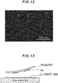
- FIG. 12 shows a polarized light microscope image obtained by observing the organic semiconductor single crystal film disposed on the parylene from the surface of the organic semiconductor single crystal film.
- FIG. 13 is a schematic drawing showing a state of transferring the organic semiconductor single crystal film formed on the mica substrate onto the PDMS/PET substrate having Au electrodes.
- FIG. 14 shows polarized light microscopic images obtained by observing the organic semiconductor single crystal film disposed on the Au and the PDMS/PET substrate from the surface of the organic semiconductor single crystal film.
- the parylene (diX-SR(registered trademark))/polyimide (PI) substrate with the Au electrodes (S/D electrode) modified by PFBT was arranged on the organic semiconductor single crystal film formed on the Eagle glass substrate so that the Au electrodes (S/D electrode) modified by PFBT were in contact with the organic semiconductor single crystal film, water was dropped at the interface between the Eagle glass substrate and the organic semiconductor single crystal film, the organic semiconductor single crystal film was separated from the Eagle glass substrate, and the organic semiconductor single crystal film was transferred onto the Au electrode and the parylene substrate modified by PFBT as shown in FIG. 16.
- FIG. 16 is a schematic cross-sectional drawing of the organic semiconductor single crystal film disposed on the parylene (diX-SR(registered trademark))/polyimide (PI) substrate with Au electrodes modified with PFBT.
- FIG. 17 is a schematic cross-sectional drawing of the TGBC type OFET.
- FIG. 18 shows a polarized light microscopic image observed from the top surface of the manufactured TGBC type OFET.
- FIG. 19 shows a graph of the transfer characteristics representing the relationship between the gate voltage and the drain current in the saturation region.
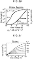
- FIG. 20 shows a graph of the transfer characteristics representing the relationship between the gate voltage and the drain current in the linear region.
- FIG. 21 shows a graph of the output characteristics representing the relationship between the drain voltage and the drain current depending on the gate voltage.
- the mobility in the saturated region was 3.2 cm 2 /V•s
- the mobility in the linear region was 4.1 cm 2 /V•s, indicating low hysteresis and relatively high mobility.
- An organic semiconductor single crystal film of the p-type organic semiconductor C 9 -DNBDT-NW of Formula (16) was formed in the same manner as in Example 1 except that an Eagle glass (manufactured by Corning) subjected to UV/ozone treatment was used as the hydrophilic substrate instead of the mica substrate.
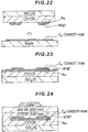
- FIG. 22 is a schematic drawing illustrating a state in which the organic semiconductor single crystal film formed on the Eagle glass substrate is transferred onto the CYTOP (registered trademark)/SiO 2 /Si substrate with the Au electrodes modified by the PFBT.
- FIG. 24 is a schematic cross-sectional drawing of a TGBC type OFET.
- FIG. 25 shows a polarized light microscopic image observed from the top surface of the fabricated TGBC type OFET.
- FIG. 26 shows a graph of the transfer characteristics representing the relationship between the gate voltage and the drain current in the saturation region.
- FIG. 27 shows a graph of the transfer characteristics representing the relationship between the gate voltage and the drain current in the linear region.
- FIG. 28 shows a graph of the output characteristics representing the relationship between the drain voltage and the drain current depending on the gate voltage.
- the mobility in the saturated region was 0.9 cm 2 /V s
- the mobility in the linear region was 1.9 cm 2 /V s
- a small hysteresis and a sharp subthreshold property were shown.
- An organic semiconductor single crystal film of the p-type organic semiconductor C 9 -DNBDT-NW of Formula (16) was formed in the same manner as in Example 1 except that an Eagle glass (manufactured by Corning) subjected to UV/ozone treatment was used as the hydrophilic substrate instead of the mica substrate.
- a CYTOP (registered trademark)/SiO 2 /Si substrate in which CYTOP (registered trademark)-809M was deposited was prepared.
Landscapes
- Engineering & Computer Science (AREA)
- Manufacturing & Machinery (AREA)
- Thin Film Transistor (AREA)
- Liquid Deposition Of Substances Of Which Semiconductor Devices Are Composed (AREA)
Abstract
Description
- The present disclosure relates to an organic semiconductor device, a method for manufacturing an organic semiconductor single crystal film, and a method for manufacturing an organic semiconductor device.
- In recent years, interest in organic semiconductors has been increasing. As features of organic semiconductors, unlike conventional inorganic semiconductors of amorphous silicon and polycrystalline silicon, it mentions that it is excellent in flexibility, that it can be inexpensively enlarged in area by roll to roll processing, etc., and applications of organic semiconductors as post-silicon semiconductors to electronic devices of the next generation type are examined.
- In particular, it is known that an organic semiconductor device having excellent characteristics can be manufactured by forming an organic semiconductor single crystal film on a hydrophobic substrate, such as a fluorine-based polymer insulating film.
- In addition, as a method for manufacturing an organic semiconductor device, a film forming method such as a coating method or a vapor phase growth method (PVT : Physical Vapor Transport) has been conventionally used (
Patent Literature 1 and Non-Patent Literature 1), and in particular, by using a coating method in a film forming method, an improvement in use efficiency of a material and a drastic cost reduction can be expected. - [PTL 1]
Japanese Unexamined Patent Publication No. 2015-185620 -
- [NPL 1] Balthasar Blulle, et al., Approaching the trap-free limit in organic single-crystal field-effect transistors, Physical Review Applied 1, 034006 (2014)
- [NPL 2] M. Kitamura et al., Work function of gold surfaces modified using substituted benzenethiols: Reaction time dependence and thermal stability, Appl. Phys. Express 7, 035701 (2014)
- However, conventionally, when using the vapor phase growth method, only the organic semiconductor single crystal film having a large thickness of about 2µm could be obtained, and it was difficult to obtain an organic semiconductor single crystal film with a thinner thickness.
- In addition, when a coating method is used, an organic semiconductor film could not be formed on a hydrophobic substrate, such as a fluorine-based polymer insulating film.
- Further, since an organic solvent is used in the coating method, it has not been possible to apply an organic semiconductor film on a solvent-soluble substrate. Therefore, for example, it has been difficult to form a pn junction structure composed of an organic semiconductor film by a coating method.
- Further, when an electrode film, such as Au, is provided on a substrate, a surface of the electrode film is modified with a self-assembled monolayer (SAM : Self-Assembled Monolayer), such as pentafluorobenzenethiol (PFBT) or 4-methylbenzenethiol (MBT), in order to control the work function of the electrode and to improve carrier implantation from the electrode to the organic semiconductor. However, PFBT film and the MBT film have low heat resistance, and the work function control effect is lowered at about 130 to 150 °C for PFBT and about 100 °C for the MBT (Non-Patent Literature 2). Since the coating method is often performed by heating the substrate to about 80 to 150° C, it is sometimes inappropriate to form an organic semiconductor on a substrate having an electrode film of Au or the like by the coating method.
- Thus, when using the vapor phase growth method, it has been impossible to obtain an organic semiconductor single crystal film having a thin film thickness, and when using the coating method, there has been a limitation on the substrate.
- Therefore, there has been a need for an organic semiconductor single crystal film that can be disposed on a desired substrate and that has a film thickness thinner than the conventional.
-
- (1) An organic semiconductor device comprising: a substrate; and an organic semiconductor single crystal film on the substrate, wherein an average film thickness of the organic semiconductor single crystal film is 2 to 100 nm, and at least a portion of a surface of the substrate in contact with the organic semiconductor single crystal film is hydrophobic, solvent soluble, non-heat resistant, or a combination thereof.
- (2) The organic semiconductor device according to (1) above, wherein an area of the organic semiconductor single crystal film is equal to or greater than 2 mm2.
- (3) A method for manufacturing an organic semiconductor single crystal film, comprising: forming an organic semiconductor single crystal film having an average film thickness of 2 to 100 nm on a hydrophilic and non-water-soluble first substrate using a coating method; and separating the organic semiconductor single crystal film from the first substrate by applying water to an interface between the first substrate and the organic semiconductor single crystal film.
- (4) The method for manufacturing an organic semiconductor single crystal film according to (3) above, wherein an area of the organic semiconductor single crystal film is equal to or greater than 2 mm2.
- (5) The method for manufacturing an organic semiconductor single crystal film according to (3) or (4) above, wherein a contact angle of the first substrate is smaller than a contact angle of the organic semiconductor single crystal film, and the difference in the contact angles between the first substrate and the organic semiconductor single crystal film is 80 degrees or more.
- (6) The method for manufacturing an organic semiconductor single crystal film according to any one of (3) to (5) above, wherein the applying water to the interface between the first substrate and the organic semiconductor single crystal film comprises immersing the first substrate on which the organic semiconductor single crystal film is formed in water.
- (7) A method for manufacturing an organic semiconductor device, comprising disposing the organic semiconductor single crystal film manufactured by the method for manufacturing an organic semiconductor single crystal film according to any one of (3) to (6) above on a second substrate, wherein at least a part of a surface of the second substrate in contact with the organic semiconductor single crystal film is hydrophobic, solvent soluble, non-heat resistant, or a combination thereof.
- (8) The method for manufacturing an organic semiconductor device according to (7) above, wherein the disposing the organic semiconductor single crystal film on the second substrate comprises disposing the second substrate so as to be in contact with the organic semiconductor single crystal film formed on the first substrate while applying water to the interface between the first substrate and the organic semiconductor single crystal film to separate the organic semiconductor single crystal film from the first substrate and dispose the organic semiconductor single crystal film on the second substrate.
- (9) The method for manufacturing an organic semiconductor device according to (7) or (8) above, wherein the at least a portion of the surface of the second substrate in contact with the organic semiconductor single crystal film has at least one of a concave portion, a convex portion, an uneven portion, and an electrode.
- According to the present disclosure, it is possible to obtain an organic semiconductor single crystal film that can be disposed on a desired substrate and has a thickness thinner than that of a conventional film.
-
-
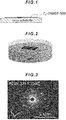
FIG. 1 is a cross-sectional schematic drawing of an organic semiconductor single crystal film formed on a mica substrate. -
FIG. 2 is a schematic drawing showing a state in which a hydrophilic substrate on which an organic semiconductor single crystal film is formed is immersed in water and the organic semiconductor single crystal film floats on a water surface. -
FIG. 3 is an electron diffraction pattern of a resulting organic semiconductor single crystal film obtained by transmission electron microscopy (TEM) observation. -
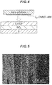
FIG. 4 is a schematic drawing illustrating a state of transferring an organic semiconductor single crystal film formed on a mica substrate onto a CYTOP (registered trademark)/SiO2/Si substrate. -
FIG. 5 is a polarized light microscopic image of an organic semiconductor single crystal film disposed on CYTOP (registered trademark) observed from the surface. -
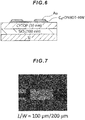
FIG. 6 is a cross-sectional schematic drawing of an organic semiconductor single crystal film and an Au electrode disposed on a CYTOP (registered trademark)/SiO2/Si substrate. -
FIG. 7 is a polarized light microscopic image of a fabricated BGTC type OFET observed from the top surface. -
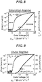
FIG. 8 is a graph of transfer characteristics showing the relationship between gate voltage and drain current in the saturation region. -
FIG. 9 is a graph of transfer characteristics showing the relationship between gate voltage and drain current in the linear region. -
FIG. 10 is a graph of output characteristics showing the relationship between drain voltage and drain current depending on the gate voltage. -
FIG. 11 is a schematic drawing illustrating a state in which an organic semiconductor single crystal film formed on a mica substrate is transferred onto a parylene/SiO2/Si substrate. -
FIG. 12 is a polarized light microscope image of an organic semiconductor single crystal film disposed on parylene, observed from the surface. -
FIG. 13 is a schematic drawing showing a state in which an organic semiconductor single crystal film formed on a mica substrate is transferred onto a PDMS/PET substrate having Au electrodes. -
FIG. 14 is a polarized light microscopic image of an organic semiconductor single crystal film disposed on an Au and a PDMS/PET substrate observed from the surface. -
FIG. 15 is a schematic drawing showing a state in which an organic semiconductor single crystal film formed on an Eagle glass substrate is transferred onto a parylene/polyimide substrate with Au electrodes. -
FIG. 16 is a schematic cross-sectional drawing of an organic semiconducting single crystal film disposed on a parylene (diX-SR(registered trademark))/polyimide (PI) substrate with Au electrodes modified with PFBT. -
FIG. 17 is a schematic cross-sectional drawing of a top-gate bottom-contact (TGBC)-type organic field-effect transistor (OFET). -
FIG. 18 is a polarized light microscopic image of a manufactured TGBC type OFET observed from the top surface. -
FIG. 19 is a graph showing the relationship between gate voltage and drain current in the saturation region. -
FIG. 20 is a graph showing the relationship between gate voltage and drain current in the linear region. -
FIG. 21 is a graph showing the relationship between drain voltage and drain current depending on the gate voltage. -
FIG. 22 is a schematic drawing illustrating a state in which an organic semiconducting single crystal film formed on an Eagle glass is transferred onto a CYTOP (registered trademark)/SiO2/Si substrate having Au electrodes modified by PFBT. -
FIG. 23 is a schematic cross-sectional drawing of an organic semiconductor single crystal film disposed on a CYTOP (registered trademark)/SiO2/Si substrate having Au electrodes modified with PFBT. -
FIG. 24 is a cross-sectional schematic drawing of a top-gate bottom-contact (TGBC) type organic field-effect transistor (OFET). -
FIG. 25 is a polarized light microscopic image observed from a top surface of a manufactured TGBC type OFET. -
FIG. 26 is a graph showing the relationship between gate voltage and drain current in the saturation region. -
FIG. 27 is a graph showing the relationship between gate voltage and drain current in the linear region. -
FIG. 28 is a graph showing the relationship between drain voltage and drain current depending on gate voltage. -
FIG. 29 is a confocal laser microscopic image of an organic semiconductor single crystal film, which is observed from the surface, formed on an Eagle glass substrate and transferred onto a CYTOP (registered trademark)/SiO2/Si substrate. -
FIG. 30 is a result obtained from a single crystal X-ray diffraction experiment of the obtained organic semiconductor single crystal film. - The present disclosure is directed to an organic semiconductor device comprising: a substrate; and an organic semiconductor single crystal film on the substrate, wherein an average film thickness of the organic semiconductor single crystal film is 2 to 100 nm, and at least a portion of a surface of the substrate in contact with the organic semiconductor single crystal film is hydrophobic, solvent soluble, non-heat resistant, or a combination thereof.
- The average film thickness of the organic semiconductor single crystal film in the organic semiconductor device of the present disclosure is 2 to 100 nm, preferably 4 to 20 nm. By having the average film thickness of the organic semiconductor single crystal film in the range, good device characteristics can be obtained. The average film thickness of the organic semiconductor single crystal film can be measured using a stylus type surface profile measuring instrument or an atomic force microscope.
- The organic semiconductor single crystal film in the organic semiconductor device of the present disclosure preferably has 1 molecular layer to 50 molecular layers, more preferably 1 molecular layer to 10 molecular layers, and still more preferably 1 molecular layer to 5 molecular layers in the thickness direction. The organic semiconductor single crystal film in the organic semiconductor device of the present disclosure most preferably has one molecular layer, but may have two or more molecular layers in the thickness direction. The number of molecular layers of the organic semiconductor single crystal film can be measured by an atomic force microscope.
- The thickness of one molecular layer of the organic semiconductor single crystal film in the organic semiconductor device of the present disclosure is preferably 2 to 6 nm, more preferably 2 to 4 nm. The thickness of one molecular layer of the organic semiconductor single crystal film can be measured by combining with single crystal X-ray structure analysis and atomic force microscope observation.
- The area of the organic semiconductor single crystal film in the organic semiconductor device of the present disclosure is preferably 2 mm2 or more, more preferably 10 mm2 or more, even more preferably 100 mm2 or more, even more preferably 1000 mm2 or more, and even more preferably 10000 mm2 or more. The upper limit of the area of the organic semiconductor single crystal film is not particularly limited, and may be limited by the size of the manufacturing facility and may be, for example, 10m2. Conventionally, when a vapor phase growth method is used, only an organic semiconductor single crystal film having an area of at most about 1 mm2 could be obtained, whereas the organic semiconductor device of the present disclosure can have a large area as described above.
- The organic semiconductor single crystal film in the organic semiconductor device of the present disclosure is composed of a single domain or multi-domain, and preferably is composed of a single domain. The domain of the organic semiconductor single crystal film can be measured by single crystal X-ray diffraction. The organic semiconductor single crystal film of the organic semiconductor device of the present disclosure preferably has a single domain with a contiguous area of 0.005 mm2 or more, more preferably 0.5 mm2 or more, and even more preferably 2.0 mm2 or more.
- The organic semiconductor single crystal film in the organic semiconductor device of the present disclosure exhibits a mobility of preferably 0.5 cm2/V•s or more, more favorably 3.0 cm2/V•s or more, more favorably 5.0cm2/V•s or more, more favorably 7.5 cm2/V•s or more, and more favorably 10 cm2/V•s or more. The mobility of the organic semiconductor single crystal film can be calculated from the measurement results of the organic field effect transistor.
- In the organic semiconductor device of the present disclosure, at least a portion of the surface of the substrate in contact with the organic semiconductor single crystal film has characteristics of hydrophobicity, solvent solubility, non-heat resistance, or a combination thereof. Preferably, the entire surface of the substrate in contact with the organic semiconductor single crystal film has the characteristics of hydrophobicity, solvent solubility, non-heat resistance, or a combination thereof, and more preferably, the entire substrate has the characteristics of hydrophobicity, solvent solubility, non-heat resistance, or a combination thereof.
- In the present application, hydrophobicity may have preferably a contact angle of 80 degrees or more, more preferably a contact angle of 90 degrees or more, still more preferably 100 degrees or more, still more preferably 110 degrees or more, and still more preferably 150 degrees or more.
- In the organic semiconductor device of the present disclosure, at least a part of the surface of the substrate in contact with the organic semiconductor single crystal film, preferably the entire surface of the substrate in contact with the organic semiconductor single crystal film, more preferably the entire substrate exhibits hydrophobicity in the above preferable range, whereby when a device is manufactured using an organic semiconductor single crystal film disposed on the hydrophobic substrate, moisture (adsorbed molecules) that can be attached to the substrate can be reduced or eliminated, and a device having favorable characteristics without influence of moisture can be manufactured.
- Examples of the hydrophobic substrate include parylene (contact angle: about 80 to 90 degrees), CYTOP (registered trademark) (contact angle: 110 degrees) which is a fluorine-based polymer, and the like.
- In the present application, the solvent soluble means substantially dissolving, decomposing, or swelling in an organic solvent, and means substantially dissolving, decomposing, or swelling with respect to an organic solvent conventionally used in a coating method, for example, toluene, dichlorobenzene, or the like.
- In the organic semiconductor device of the present disclosure, at least a part of the surface of the substrate in contact with the organic semiconductor single crystal film, preferably the entire surface of the substrate in contact with the organic semiconductor single crystal film, more preferably the entire substrate may be soluble in a solvent. Therefore, at least a part of the surface of the substrate in contact with the organic semiconductor single crystal film, preferably the entire surface of the substrate in contact with the organic semiconductor single crystal film, more preferably the entire substrate may be a p-type organic semiconductor film or an n-type organic semiconductor film, or may be a laminate comprising a p-type organic semiconductor film and an n-type organic semiconductor film. Therefore, the substrate in the electronic device of the present disclosure may include a pn junction structure, a pnp junction structure, or an npn junction structure formed of an organic semiconductor film.
- In the present application, the non-heat resistance preferably means that the glass transition point is 90 ° C or less, or sublimation, melting, or decomposition occurs at 90 ° C or less, and more preferably means that the glass transition point is 120 ° C or less, or sublimation, melting, or decomposition occurs at 120 ° C or less.
- In the organic semiconductor device of the present disclosure, at least a part of the surface of the substrate in contact with the organic semiconductor single crystal film, preferably the entire surface of the substrate in contact with the organic semiconductor single crystal film, more preferably the entire substrate may be non-heat resistant. Therefore, at least a part of the surface of the substrate in contact with the organic semiconductor single crystal film, preferably the entire surface of the substrate in contact with the organic semiconductor single crystal film, more preferably the entire substrate, may be a substrate having an electrode film of Au or the like modified with a self-assembled monolayer (SAM: self-assembled monolayer), such as pentafluorobenzene thiol (PFBT), for example. The organic semiconductor single crystal film can be disposed on such a modifying material having low heat resistance, such as PFBT or the like.
- The type of the organic semiconductor constituting the organic semiconductor single crystal film in the organic semiconductor device of the present disclosure is not particularly limited, and for example, a polycyclic aromatic compound of four or more rings, or a polycyclic compound of four or more rings formed of one or more unsaturated five-membered heterocyclic compounds and a plurality of benzene rings can be used.
- The organic semiconductor constituting the organic semiconductor single-crystal film in the organic semiconductor device of the present disclosure is preferably a material having a high self-aggregation ability, such as a p-type organic semiconductor Cn-DNBDT-NW of the following formula (1) exhibiting a high mobility.

- Other examples of the organic semiconductor constituting the organic semiconductor single crystal film in the organic semiconductor device of the present disclosure are shown in the following formulas (2) to (6).

- In the polythiophene semiconductor represented by Formula (2), R1 and R2 are each independently a hydrogen atom or an alkyl group having 4 to 10 carbon atoms. The alkyl group may comprise a heteroatom (typically selected from an oxygen atom and a sulfur atom). In addition, R1 and R2 together can form a ring. For reasons of self-aggregation ability, preferably, R1 and R2 are each independently a hydrogen atom or an alkyl group having 5 to 8 carbon atoms. More preferably, each of R1 and R2 is independently a hydrogen atom or a hexyl group.
- The n represents an integer of 5 to 100. The n indicates the average number of thiophene monomer units in the polythiophene semiconductor, i.e., the length of the polythiophene chain. From the viewpoint of forming the single crystal film, the n is preferably 50 or less.

- In Formula (3), each of R3, R4, R5 and R6 is independently a hydrogen atom or an alkyl group having 1 to 14 carbon atoms. The alkyl group may comprise a heteroatom (typically selected from an oxygen atom and a sulfur atom), and the hydrogen atom in the alkyl group may be substituted with a substituent, such as a halogen atom. For reasons of self-aggregation ability, R4=R5 is preferred, and R3=R6 is preferred. From the viewpoint of solubility, preferably, R4 and R5 are hydrogen atoms, and R3 and R6 are each independently an alkyl group having 1 to 14 carbon atoms, or R3 and R6 are hydrogen atoms, and R4 and R5 are each independently an alkyl group having 1 to 14 carbon atoms. More preferably, R3 and R6 are hydrogen atoms, and R4 and R5 are each independently an alkyl group having 1 to 14 carbon atoms. For reasons of self-aggregation ability, the carbon number of the alkyl group is preferably from 4 to 12, more preferably from 6 to 10.

- In Formula (4), each of R7, R8, R9 and R10 is independently a hydrogen atom or an alkyl group having 1 to 14 carbon atoms. The alkyl group may comprise a heteroatom (typically selected from an oxygen atom and a sulfur atom), and the hydrogen atom in the alkyl group may be substituted with a substituent, such as a halogen atom. For reasons of self-aggregation ability, R7=R9 is preferred, and R8=R10 is preferred. From the viewpoint of solubility, preferably, R7 and R9 are hydrogen atoms, and R8 and R10 are each independently an alkyl group having 1 to 14 carbon atoms, or R8 and R10 are hydrogen atoms, and R7 and R9 are each independently an alkyl group having 1 to 14 carbon atoms. More preferably, R8 and R10 are hydrogen atoms, and R7 and R9 are each independently an alkyl group having 1 to 14 carbon atoms. For reasons of self-aggregation ability, the carbon number of the alkyl group is preferably from 6 to 13, more preferably from 8 to 10.

- In Formula (5), each of R11, R12, R13 and R14 is independently a hydrogen atom or an alkyl group having 1 to 14 carbon atoms. The alkyl group may comprise a heteroatom (typically selected from an oxygen atom and a sulfur atom), and the hydrogen atom in the alkyl group may be substituted with a substituent, such as a halogen atom. For reasons of self-aggregation ability, R11=R13 is preferred, and R12=R14 is preferred. From the viewpoint of solubility, preferably, R11 and R13 are hydrogen atoms, and R12 and R14 are each independently an alkyl group having 1 to 14 carbon atoms, or R12 and R14 are hydrogen atoms, and R11 and R13 are each independently an alkyl group having 1 to 14 carbon atoms. More preferably, R12 and R14 are hydrogen atoms, and R11 and R13 are each independently an alkyl group having 1 to 14 carbon atoms. For reasons of self-aggregation ability, the number of carbon atoms of the alkyl group is preferably from 5 to 12, more preferably from 8 to 10.

- In formula (6), R15, R16, R17 and R18 are each independently a hydrogen atom or an alkyl group having 1 to 14 carbon atoms. The alkyl group may comprise a heteroatom (typically selected from an oxygen atom and a sulfur atom), and the hydrogen atom in the alkyl group may be substituted with a substituent, such as a halogen atom. For reasons of self-aggregation ability, R15=R17 is preferred, and R16=R18 is preferred. From the viewpoint of solubility, preferably, R16 and R18 are hydrogen atoms, and R15 and R17 are each independently an alkyl group having 1 to 14 carbon atoms, or R15 and R17 are hydrogen atoms, and R16 and R18 are each independently an alkyl group having 1 to 14 carbon atoms. More preferably, R16 and R18 are hydrogen atoms, and R15 and R17 are each independently an alkyl group having 1 to 14 carbon atoms. For reasons of self-aggregation ability, the number of carbon atoms of the alkyl group is preferably from 5 to 12, more preferably from 8 to 10.
- Yet another examples of the organic semiconductor constituting the organic semiconductor single crystal film in the organic semiconductor device of the present disclosure are shown in the following formulas (7) to (15). In Formula (7) to Formula (15), R may be linear alkyl, branched alkyl, fluorinated linear/branched alkyl, triisopropylsilylethynyl, phenyl, or the like.


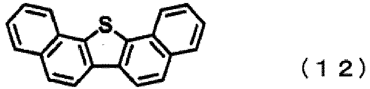


- The organic semiconductor single crystal film can be confirmed to be single crystal by observing the organic semiconductor single crystal film with a transmission electron microscope (TEM).
- The organic semiconductor device of the present disclosure can be an organic EL (electroluminescence) element, an organic solar cell element, an organic photoelectric conversion element, an organic transistor element, an organic field effect transistor element, or the like.
- The present disclosure is also directed to a method for manufacturing an organic semiconductor single crystal film, comprising: forming an organic semiconductor single crystal film having an average film thickness of 2 to 100 nm on a hydrophilic and non-water-soluble first substrate using a coating method, and separating the organic semiconductor single crystal film from the first substrate by applying water to an interface between the first substrate and the organic semiconductor single crystal film.
- According to the method for manufacturing an organic semiconductor single crystal film of the present disclosure, it is possible to provide an organic semiconductor single crystal film that can be disposed on a desired substrate and has a thickness thinner than that of a conventional film.
- In the method for manufacturing an organic semiconductor single crystal film of the present disclosure, an organic semiconductor single crystal film having an average film thickness of 2 to 100 nm is formed on a hydrophilic and non-water-soluble first substrate by a coating method. The coating method is a method in which an organic semiconductor is dissolved in an organic solvent to prepare an organic semiconductor solution, the organic semiconductor solution is applied on a substrate, and the organic solvent is evaporated to form a film. As the organic solvent, an organic solvent conventionally used in a coating method can be used, and for example, toluene, dichlorobenzene, or the like can be used.
- In the method for manufacturing an organic semiconductor single crystal film of the present disclosure, a method conventionally used can be used as a coating method, and for example, an edge casting method, a continuous edge casting method, a drop casting method, a spin coating method, a printing method (ink jet method or gravure printing method), a dispenser method, a spray method, a dip coating method, a die coater method, a roll coater method, a bar coater method, a blade coating method, or the like can be used.
- The first substrate is a hydrophilic substrate having a contact angle of water of preferably 20 degrees or less, more preferably 10 degrees or less. The first substrate is non-water-soluble and can be, for example, mica or glass. Since the first substrate is non-water-soluble, when water is applied to the interface between the first substrate and the organic semiconductor single crystal film, components of the first substrate are not eluted and do not adhere to or react with the organic semiconductor single crystal film, so that a high-purity organic semiconductor single crystal film can be obtained. Further, when applying water to the interface between the first substrate and the organic semiconductor single crystal film, in order to maintain the shape of the first substrate without collapsing, it is possible to separate the organic semiconductor single crystal film from the first substrate without distorting the shape of the organic semiconductor single crystal film. The non-water-soluble means that it does not substantially dissolve, decompose, or swell in water. The glass is preferably subjected to a hydrophilic treatment on the surface by UV-ozone treatment or a hydrophilic coating material or the like.
- Water is applied to the interface between the first substrate and the organic semiconductor single crystal film to separate the organic semiconductor single crystal film from the first substrate. Since a molecule of the organic semiconductor single crystal film applied to the first substrate is hydrophobic, water enters between the hydrophilic first substrate and the molecule of the hydrophobic organic semiconductor single crystal film, and the organic semiconductor single crystal film can be separated from the first substrate.
- The water contact angle of the hydrophilic first substrate is smaller than the water contact angle of the hydrophobic organic semiconductor single crystal film, and the difference in the water contact angle between the first substrate and the organic semiconductor single crystal film is preferably 80 degrees or more, more preferably 90 degrees or more. The contact angle of the organic semiconductor single crystal film is preferably 100 to 120 degrees. When the difference in the contact angle between the hydrophilic first substrate and the hydrophobic organic semiconductor single crystal film is within the preferable range, the organic semiconductor single crystal film can be more stably peeled off from the first substrate.
- The method of applying water to the interface between the first substrate and the organic semiconductor single crystal film is not particularly limited, and may include immersing the first substrate on which the organic semiconductor single crystal film is formed in water, dropping a dropper of water at the interface between the first substrate and the organic semiconductor single crystal film, or the like.
- The method of applying water to the interface between the first substrate and the organic semiconductor single crystal film preferably comprises immersing the first substrate on which the organic semiconductor single crystal film is formed in water. By immersing the first substrate on which the organic semiconductor single crystal film is formed in water, the organic semiconductor single crystal film is separated from the first substrate in water, and an organic semiconductor single crystal film which is self-standing in water can be obtained. The self-standing organic semiconductor single crystal film can be disposed on any substrate, such as a hydrophobic substrate, a solvent-soluble substrate, a non-heat-resistant substrate, or a substrate having a concave portion, a convex portion, an uneven portion, or an electrode, or a mesh-shaped or grid-shaped substrate in the organic semiconductor device described above.
- With respect to the average film thickness, molecular layer, area, domain, and mobility of the organic semiconductor single crystal film obtained by the method for manufacturing the organic semiconductor single crystal film of the present disclosure, the contents relating to the organic semiconductor single crystal film in the organic semiconductor device described above can be applied.
- The present disclosure is also directed to a method for manufacturing an organic semiconductor device, comprising disposing an organic semiconductor single crystal film manufactured by the method for manufacturing an organic semiconductor single crystal film described above on a second substrate, wherein at least a portion of a surface of the second substrate in contact with the organic semiconductor single crystal film is hydrophobic, solvent soluble, non-heat resistant, or a combination thereof.
- In the method for manufacturing an organic semiconductor device of the present disclosure, the organic semiconductor single crystal film separated from the first substrate by the method for manufacturing the organic semiconductor single crystal film described above is disposed on the second substrate.
- At least a portion of the surface of the second substrate on which the organic semiconductor single crystal film is disposed in contact with the organic semiconductor single crystal film has characteristics of hydrophobicity, solvent solubility, non-heat resistance, or a combination thereof. Preferably, the entire surface of the second substrate in contact with the organic semiconductor single crystal film has the characteristics of hydrophobicity, solvent solubility, non-heat resistance, or a combination thereof, and more preferably, the entire second substrate has the characteristics of hydrophobicity, solvent solubility, non-heat resistance, or a combination thereof.
- As for the contents relating to the hydrophobicity, the solvent solubility, and the non-heat resistance of the second substrate, the contents described in terms of the hydrophobicity, the solvent solubility, and the non-heat resistance of the substrate of the organic semiconductor device described above can be applied.
- The disposing the organic semiconductor single crystal film on the second substrate preferably comprises separating the organic semiconductor single crystal film from the first substrate by applying water to the interface between the first substrate and the organic semiconductor single crystal film while disposing the second substrate so as to be in contact with the organic semiconductor single crystal film formed on the first substrate, and disposing the organic semiconductor single crystal film on the second substrate. By thus separating the organic semiconductor single crystal film from the first substrate while disposing the second substrate so as to contact the organic semiconductor single crystal film, it is possible to transfer the organic semiconductor single crystal film directly from the first substrate to the second substrate.
- Alternatively, the disposing the organic semiconductor single crystal film on the second substrate preferably comprises immersing the first substrate having the organic semiconductor single crystal film formed thereon in water, separating the organic semiconductor single crystal film from the first substrate in water to obtain a self-standing organic semiconductor single crystal film, and disposing the organic semiconductor single crystal film on the second substrate in water. Thus, in water, by disposing a free-standing organic semiconductor single crystal film on the second substrate, it is possible to easily transfer the organic semiconductor single crystal film from the first substrate to the second substrate.
- More preferably, the disposing the organic semiconductor single crystal film on the second substrate comprises immersing the first substrate, the organic semiconductor single crystal film, and the second substrate in water while disposing the second substrate so as to be in contact with the organic semiconductor single crystal film formed on the first substrate, and transferring the organic semiconductor single crystal film from the first substrate to the second substrate. In this manner, by separating the organic semiconductor single crystal film from the first substrate while disposing the second substrate in contact with the organic semiconductor single crystal film in water, the organic semiconductor single crystal film can be more easily transferred from the first substrate to the second substrate.
- At least a portion of the surface in contact with the organic semiconductor single crystal film of the second substrate may have at least one of a concave portion, a convex portion, an uneven portion, and an electrode.
- Conventionally, when fabricating a transistor having a top gate structure by a coating method, it is necessary to apply an organic semiconductor on a substrate in which an electrode is arranged, due to the difference in surface energy between the electrode and the substrate, and the difference in step between the convex portion of the electrode and the concave portion of the substrate, the crystallinity and thickness of the organic semiconductor cannot be uniformly formed, making it difficult to obtain good transistor characteristics.
- According to the method for manufacturing an organic semiconductor of the present disclosure, even if the second substrate has an electrode, the organic semiconductor single crystal film peeled off from the first substrate is brought into contact with the second substrate, whereby the organic semiconductor single crystal film can be disposed with a uniform thickness on the second substrate having the electrode.
- The second substrate may have a concave portion, a convex portion, or an uneven portion, attributable to the electrode or not attributable to the electrode. The concave portion, convex portion, or an uneven portion can be rectangular in shape, curved in shape, or a combination thereof. The depth of the concave portion, the height of the convex portion, and the depth of the uneven portion (the distance in the thickness direction of the substrate between the lowest portion of the concave portion and the highest portion of the convex portion) on the second substrate are each preferably greater than 0 nm and equal to or less than 30 nm.
- A natural mica substrate was prepared as a hydrophilic substrate. As an organic semiconductor, a powder of p-type organic semiconductor C9-DNBDT-NW of the following formula (16), which shows high mobility, was prepared.

FIG. 1 was formed on the substrate. The water contact angle on the surface of the organic semiconductor single crystal film was 108 degrees.FIG. 1 is a cross-sectional schematic drawing of the organic semiconductor single crystal film formed on the mica substrate. - As shown in
FIG. 2 , the hydrophilic substrate on which the organic semiconductor single crystal film was formed was immersed in water, and the organic semiconductor single crystal film was peeled off from the hydrophilic substrate. The organic semiconductor single crystal film was in a free standing state at the water surface. The free standing state at the water surface means that the organic semiconductor single crystal film is floating on the water surface while maintaining the crystal structure without the supporting substrate.FIG. 2 is a schematic drawing showing a state in which a hydrophilic substrate on which an organic semiconductor single crystal film is formed is immersed in water. -
FIG. 3 shows an electron diffraction pattern obtained by transmission electron microscopy (TEM) observation of the obtained organic semiconductor single crystal film. It was confirmed that the organic semiconductor single crystal film maintained single crystallinity even after the separation from the hydrophilic substrate. - In the same manner as in Example 1, an organic semiconductor single crystal film of the p-type organic semiconductor C9-DNBDT-NW of Formula (16) was formed on a mica substrate.
- As a hydrophobic substrate, a CYTOP (registered trademark)/SiO2/Si substrate in which CYTOP (registered trademark)-809M was deposited was prepared.
- As shown in
FIG. 4 , the CYTOP (registered trademark)/SiO 2/Si substrate was arranged so that CYTOP (registered trademark) was in contact with the organic semiconductor single crystal film formed on the mica substrate, water was dropped at the interface between the mica substrate and the organic semiconductor single crystal film, and the organic semiconductor single crystal film was peeled from the mica substrate and transferred onto CYTOP (registered trademark).FIG. 4 is a schematic drawing illustrating a state of transferring the organic semiconductor single crystal film formed on the mica substrate onto the CYTOP (registered trademark)/SiO2/Si substrate.FIG. 5 shows a polarized light microscopic image obtained by observing the organic semiconductor single-crystal film disposed on the CYTOP (registered trademark) from the surface of the organic semiconductor single crystal film. - As shown in
FIG. 6 , Au electrodes having a length of 0.4 mm, a width of 2 mm, and a height of 40 nm were formed as an S/D electrode (source/drain electrode) on the organic semiconductor single crystal film of C9-DNBDT-NW disposed on the CYTOP (registered trademark)/SiO2/Si substrate by vacuum deposition using a metal mask, thereby fabricating a bottom gate top contact (BGTC) type organic field-effect transistor (OFET).FIG. 6 is a cross-sectional schematic drawing of the organic semiconductor single crystal film and the Au electrodes disposed on the CYTOP (registered trademark)/SiO2/Si substrate.FIG. 7 shows a polarized light microscopic image observed from the top surface of the fabricated BGTC type OFET. -
FIG. 8 shows a graph of the transfer characteristics representing the relationship between the gate voltage and the drain current in the saturation region.FIG. 9 shows a graph of the transfer characteristics representing the relationship between the gate voltage and the drain current in the linear region.FIG. 10 shows a graph of the output characteristics representing the relationship between the drain voltage and the drain current depending on the gate voltage. The mobility in the saturated region was 13 cm2/V·s, and the mobility in the linear region was 10 cm2/V·s, which were very large mobility. - In the same manner as in Example 1, an organic semiconductor single crystal film of the p-type organic semiconductor C9-DNBDT-NW of Formula (16) was formed on a mica substrate.
- As a hydrophobic substrate, a parylene/SiO 2/Si substrate in which parylene (diX-SR (registered trademark)) was deposited was prepared.
- As shown in
FIG. 11 , the parylene/SiO/Si substrate was positioned so that the parylene was in contact with the organic semiconductor single crystal film formed on the mica substrate, water was dropped at the interface between the mica substrate and the organic semiconductor single crystal film, and the organic semiconductor single crystal film was peeled from the mica substrate and transferred onto the parylene.FIG. 11 is a schematic drawing illustrating a state of transferring the organic semiconductor single crystal film formed on the mica substrate onto the parylene/SiO/Si substrate.FIG. 12 shows a polarized light microscope image obtained by observing the organic semiconductor single crystal film disposed on the parylene from the surface of the organic semiconductor single crystal film. - In the same manner as in Example 1, an organic semiconductor single crystal film of the p-type organic semiconductor C9-DNBDT-NW of Formula (16) was formed on a mica substrate.
- As a solvent-soluble substrate, as shown in
FIG. 13 , a polydimethylsiloxane (PDMS)/polyethylene terephthalate (PET) substrate on which Au electrodes having a length of 0.5 mm, a width of 0.5 mm, and a height of 30 nm were formed as S/D electrodes (source/drain electrodes) by vacuum deposition using a metal mask was prepared.FIG. 13 is a schematic drawing showing a state of transferring the organic semiconductor single crystal film formed on the mica substrate onto the PDMS/PET substrate having Au electrodes. - As shown in
FIG. 14 , the PDMS/PET substrate on which Au was vacuum-deposited as a source/drain (S/D) electrode was disposed so that the Au was in contact with the organic semiconductor single crystal film formed on the mica substrate, water was dropped at the interface between the mica substrate and the organic semiconductor single crystal film, and the organic semiconductor single crystal film was peeled off from the mica substrate and transferred onto the Au and the PDMS/PET substrate.FIG. 14 shows polarized light microscopic images obtained by observing the organic semiconductor single crystal film disposed on the Au and the PDMS/PET substrate from the surface of the organic semiconductor single crystal film. - An organic semiconductor single crystal film of the p-type organic semiconductor C9-DNBDT-NW of Formula (16) was formed in the same manner as in Example 1 except that an Eagle glass (manufactured by Corning) subjected to UV/ozone treatment was used as an hydrophilic substrate instead of the mica substrate.
- As a hydrophobic substrate, a parylene (diX-SR (registered trademark))/polyimide (PI) substrate with Au electrodes as S/D electrodes (source/drain electrodes) was prepared as shown in
FIG. 15 , wherein the Au electrode was formed by vacuum deposition using a metal mask, had a length of 0.4 mm, a width of 2 mm, and a height of 12 nm, and was modified with a self-assembled monolayer of pentafluorobenzenethiol (PFBT).FIG. 15 is a schematic drawing showing a state in which the organic semiconductor single crystal film formed on the Eagle glass substrate is transferred onto the parylene/polyimide substrate with the Au electrodes. - The parylene (diX-SR(registered trademark))/polyimide (PI) substrate with the Au electrodes (S/D electrode) modified by PFBT was arranged on the organic semiconductor single crystal film formed on the Eagle glass substrate so that the Au electrodes (S/D electrode) modified by PFBT were in contact with the organic semiconductor single crystal film, water was dropped at the interface between the Eagle glass substrate and the organic semiconductor single crystal film, the organic semiconductor single crystal film was separated from the Eagle glass substrate, and the organic semiconductor single crystal film was transferred onto the Au electrode and the parylene substrate modified by PFBT as shown in
FIG. 16. FIG. 16 is a schematic cross-sectional drawing of the organic semiconductor single crystal film disposed on the parylene (diX-SR(registered trademark))/polyimide (PI) substrate with Au electrodes modified with PFBT. - Further, as shown in
FIG. 17 , CYTOP (registered trademark), Parylene (diX-SR (registered trademark)), and gate electrodes were formed on C9-DNBDT-NW of the organic semiconductor single crystal film, and a top gate bottom contact (TGBC) type organic field-effect transistor (OFET) was manufactured.FIG. 17 is a schematic cross-sectional drawing of the TGBC type OFET.FIG. 18 shows a polarized light microscopic image observed from the top surface of the manufactured TGBC type OFET. -
FIG. 19 shows a graph of the transfer characteristics representing the relationship between the gate voltage and the drain current in the saturation region.FIG. 20 shows a graph of the transfer characteristics representing the relationship between the gate voltage and the drain current in the linear region.FIG. 21 shows a graph of the output characteristics representing the relationship between the drain voltage and the drain current depending on the gate voltage. The mobility in the saturated region was 3.2 cm2/V•s, and the mobility in the linear region was 4.1 cm2/V•s, indicating low hysteresis and relatively high mobility. - An organic semiconductor single crystal film of the p-type organic semiconductor C9-DNBDT-NW of Formula (16) was formed in the same manner as in Example 1 except that an Eagle glass (manufactured by Corning) subjected to UV/ozone treatment was used as the hydrophilic substrate instead of the mica substrate.
- As a hydrophobic substrate, a CYTOP (registered trademark)/SiO2/Si substrate with Au electrodes as S/D electrodes (source/drain electrodes) was prepared as shown in
FIG. 22 , wherein the Au electrode was formed by vacuum deposition using a metal mask, had a length of 0.4 mm, a width of 2 mm, and a height of 20 nm, and was modified with a self-assembled monolayer of pentafluorobenzenethiol (PFBT).FIG. 22 is a schematic drawing illustrating a state in which the organic semiconductor single crystal film formed on the Eagle glass substrate is transferred onto the CYTOP (registered trademark)/SiO2/Si substrate with the Au electrodes modified by the PFBT. - The Eagle glass with PFBT-modified Au electrodes (S/D electrodes) was placed so that the Au electrodes (S/D electrodes) modified with PFBT were in contact with the organic semiconductor single crystal film deposited on the Eagle glass substrate. Water was dropped at the interface between the Eagle glass substrate and the organic semiconductor single crystal film, the organic semiconductor single crystal film was peeled off from the Eagle glass substrate, and the organic semiconductor single crystal film was transferred to the Au electrode modified with PFBT and the CYTOP (registered trademark) substrate as shown in
FIG. 23. FIG. 23 is a schematic cross-sectional drawing of an organic semiconductor single-crystal film disposed on CYTOP (registered trademark)/SiO2/Si substrates having Au electrodes modified with PFBT. - Further, as shown in
FIG. 24 , CYTOP (registered trademark), parylene (diX-SR (registered trademark)), and gate electrodes were formed on C9-DNBDT-NW of the organic semiconductor single crystal film to fabricate a top gate bottom contact (TGBC) type organic field-effect transistor (OFET).FIG. 24 is a schematic cross-sectional drawing of a TGBC type OFET.FIG. 25 shows a polarized light microscopic image observed from the top surface of the fabricated TGBC type OFET. -
FIG. 26 shows a graph of the transfer characteristics representing the relationship between the gate voltage and the drain current in the saturation region.FIG. 27 shows a graph of the transfer characteristics representing the relationship between the gate voltage and the drain current in the linear region.FIG. 28 shows a graph of the output characteristics representing the relationship between the drain voltage and the drain current depending on the gate voltage. The mobility in the saturated region was 0.9 cm2/V s, the mobility in the linear region was 1.9 cm2/V s, and a small hysteresis and a sharp subthreshold property were shown. - An organic semiconductor single crystal film of the p-type organic semiconductor C9-DNBDT-NW of Formula (16) was formed in the same manner as in Example 1 except that an Eagle glass (manufactured by Corning) subjected to UV/ozone treatment was used as the hydrophilic substrate instead of the mica substrate.
- As a hydrophobic substrate, a CYTOP (registered trademark)/SiO2/Si substrate in which CYTOP (registered trademark)-809M was deposited was prepared.
- The CYTOP (registered trademark)/SiO2/Si substrate was arranged so that the CYTOP (registered trademark) was in contact with the organic semiconductor single crystal film formed on the Eagle glass subjected to the UV/ozone treatment, water was dropped at the interface between the Eagle glass and the organic semiconductor single crystal film, and the organic semiconductor single crystal film of 1.7 cm2 was peeled off from the Eagle glass substrate and transferred onto the CYTOP (registered trademark).
-
FIG. 29 shows a confocal laser microscopic image of the organic semiconductor single crystal film on the CYTOP (registered trademark)/SiO2/Si substrate from the surface of the organic semiconductor single crystal film. The obtained organic semiconductor single crystal film had a single domain having a contiguous area of 20 mm2. - Twenty-four organic field-effect transistors were fabricated using the obtained organic semiconductor single crystal film, and the mobility of the saturation region and the mobility of the linear region were measured. The average mobility of the saturation region was 10.8±1.8 cm2/V·s, and the average mobility of the linear region was 9.9±2.1 cm2/V•s.
- An organic semiconductor single crystal film of the p-type organic semiconductor C9-DNBDT-NW of Formula (16) was formed in the same manner as in Example 1 except that an Eagle glass (manufactured by Corning) subjected to UV/ozone treatment was used as the hydrophilic substrate instead of the mica substrate.
- A glass substrate with a thickness of 30µm was prepared for single crystal X-ray diffraction measurement. The glass substrate was placed so as to be in contact with the organic semiconductor single crystal film formed on the Eagle glass subjected to UV and ozone treatment, and water was dropped at the interface between the organic semiconductor single crystal film and the Eagle glass substrate, and the organic semiconductor single crystal film was peeled off from the Eagle glass substrate and transferred onto the glass substrate.
-
FIG. 30 shows the single crystal X-ray diffraction measurement results of the organic semiconductor single crystal film transferred on the glass substrate. c∗ corresponds to the crystal growth direction, and a portion surrounded by a white circle indicates a diffractive peak derived from the organic semiconductor single crystal film. Single spots were obtained from single crystal X-ray diffraction measurement, and it was found that the obtained organic semiconductor single crystal film was composed of a single domain in the area of 0.00795 mm2 irradiated with X-rays.
Claims (9)
- An organic semiconductor device comprising:a substrate; andan organic semiconductor single crystal film on the substrate,wherein an average film thickness of the organic semiconductor single crystal film is 2 to 100nm, andat least a portion of a surface of the substrate in contact with the organic semiconductor single crystal film is hydrophobic, solvent soluble, non-heat resistant, or a combination thereof.
- The organic semiconductor device according to claim 1, wherein an area of the organic semiconductor single crystal film is equal to or greater than 2 mm2.
- A method for manufacturing an organic semiconductor single crystal film, comprising:forming an organic semiconductor single crystal film having an average film thickness of 2 to 100 nm on a hydrophilic and non-water-soluble first substrate using a coating method; andseparating the organic semiconductor single crystal film from the first substrate by applying water to an interface between the first substrate and the organic semiconductor single crystal film.
- The method for manufacturing an organic semiconductor single crystal film according to claim 3, wherein an area of the organic semiconductor single crystal film is equal to or greater than 2 mm2.
- The method for manufacturing an organic semiconductor single crystal film according to claim 3 or 4, wherein a contact angle of the first substrate is smaller than a contact angle of the organic semiconductor single crystal film, and the difference in the contact angles between the first substrate and the organic semiconductor single crystal film is 80 degrees or more.
- The method for manufacturing an organic semiconductor single crystal film according to any one of claims 3 to 5, wherein the applying water to the interface between the first substrate and the organic semiconductor single crystal film comprises immersing the first substrate on which the organic semiconductor single crystal film is formed in water.
- A method for manufacturing an organic semiconductor device, comprising disposing an organic semiconductor single crystal film manufactured by the method for manufacturing an organic semiconductor single crystal film according to any one of claims 3 to 6 on a second substrate, wherein at least a portion of a surface of the second substrate in contact with the organic semiconductor single crystal film is hydrophobic, solvent soluble, non-heat resistant, or a combination thereof.
- The method for manufacturing an organic semiconductor device according to claim 7, wherein the disposing the organic semiconductor single crystal film on the second substrate comprises disposing the second substrate so as to be in contact with the organic semiconductor single crystal film formed on the first substrate while applying water to the interface between the first substrate and the organic semiconductor single crystal film to separate the organic semiconductor single crystal film from the first substrate and dispose the organic semiconductor single crystal film on the second substrate.
- The method for manufacturing an organic semiconductor device according to claim 7 or 8, wherein the at least a portion of the surface of the second substrate in contact with the organic semiconductor single crystal film has at least one of a concave portion, a convex portion, an uneven portion, and an electrode.
Applications Claiming Priority (2)
| Application Number | Priority Date | Filing Date | Title |
|---|---|---|---|
| JP2019030776 | 2019-02-22 | ||
| PCT/JP2020/006597 WO2020171131A1 (en) | 2019-02-22 | 2020-02-19 | Organic semiconductor device, method for manufacturing organic semiconductor single-crystal film, and method for manufacturing organic semiconductor device |
Publications (2)
| Publication Number | Publication Date |
|---|---|
| EP3930018A1 true EP3930018A1 (en) | 2021-12-29 |
| EP3930018A4 EP3930018A4 (en) | 2022-11-09 |
Family
ID=72144044
Family Applications (1)
| Application Number | Title | Priority Date | Filing Date |
|---|---|---|---|
| EP20759235.3A Pending EP3930018A4 (en) | 2019-02-22 | 2020-02-19 | ORGANIC SEMICONDUCTOR DEVICE, METHOD FOR MAKING ORGANIC SEMICONDUCTOR SINGLE CRYSTALLINE FILM, AND METHOD FOR MAKING ORGANIC SEMICONDUCTOR DEVICE |
Country Status (6)
| Country | Link |
|---|---|
| US (1) | US20220140265A1 (en) |
| EP (1) | EP3930018A4 (en) |
| JP (1) | JP7399499B2 (en) |
| KR (1) | KR102845024B1 (en) |
| CN (1) | CN113454800B (en) |
| WO (1) | WO2020171131A1 (en) |
Families Citing this family (2)
| Publication number | Priority date | Publication date | Assignee | Title |
|---|---|---|---|---|
| JP7672648B2 (en) * | 2021-02-25 | 2025-05-08 | 国立大学法人 東京大学 | Inorganic/organic hybrid complementary semiconductor device and method for manufacturing same |
| CN116546824A (en) * | 2022-05-07 | 2023-08-04 | 浙江大学 | Organic field effect transistor and preparation method thereof |
Family Cites Families (16)
| Publication number | Priority date | Publication date | Assignee | Title |
|---|---|---|---|---|
| JP2007112748A (en) * | 2005-10-20 | 2007-05-10 | Utsunomiya Univ | Chlorine-substituted porphyrin compound and method for producing chlorine-substituted porphyrin compound |
| JP2008053265A (en) | 2006-08-22 | 2008-03-06 | Postech Foundation | Method for producing single crystal conjugated polymer nanostructures by surface-induced self-assembly |
| JP2009260268A (en) * | 2008-03-25 | 2009-11-05 | Advanced Lcd Technologies Development Center Co Ltd | Method for dehydrogenation treatment and method for forming crystalline silicon film |
| KR101149677B1 (en) * | 2010-01-20 | 2012-07-11 | 주식회사 엘지실트론 | A manufacturing method for flexible device and flexible device, solar cell, LED manufactured by the same |
| WO2012023476A1 (en) * | 2010-08-18 | 2012-02-23 | 独立行政法人産業技術総合研究所 | Method of manufacturing organic semiconductor thin film and monocrystalline organic semiconductor thin film |
| US9537110B2 (en) * | 2012-02-22 | 2017-01-03 | Jnc Corporation | Chalcogen-containing organic compound and use thereof |
| JP5945379B2 (en) | 2012-02-23 | 2016-07-05 | 国立大学法人埼玉大学 | Method for forming organic thin film and solar cell formed using the same |
| JP2014049722A (en) | 2012-09-04 | 2014-03-17 | Nec Corp | Organic semiconductor transistor and manufacturing method of the same |
| JP5787038B2 (en) * | 2013-01-07 | 2015-09-30 | 富士電機株式会社 | Transparent organic thin film transistor and manufacturing method thereof |
| JP6128665B2 (en) | 2013-04-25 | 2017-05-17 | パイクリスタル株式会社 | Manufacturing method of organic semiconductor thin film |
| JP6229924B2 (en) * | 2013-04-26 | 2017-11-15 | 国立研究開発法人物質・材料研究機構 | Method for producing large area domain organic semiconductor crystal film and large area domain organic semiconductor crystal film |
| JP6590361B2 (en) | 2014-03-20 | 2019-10-16 | パイクリスタル株式会社 | Organic semiconductor film and manufacturing method thereof |
| CN104022221A (en) * | 2014-06-20 | 2014-09-03 | 国家纳米科学中心 | Method for preparing ultra-thin and large organic small molecule single crystal wafer layer and high-quality bottom grid top contact field effect transistor of ultra-thin and large organic small molecule single crystal wafer layer |
| KR101933813B1 (en) * | 2014-09-01 | 2018-12-28 | 후지필름 가부시키가이샤 | Composition for forming organic semiconductor film, organic semiconductor film and method for manufacturing same, organic semiconductor element and method for manufacturing same, and organic semiconductor compound |
| JP6116018B2 (en) | 2015-01-29 | 2017-04-19 | 国立大学法人 東京大学 | Organic semiconductor device |
| CN109844848A (en) * | 2016-10-19 | 2019-06-04 | 奥加诺电路股份有限公司 | Active matrix LED display |
-
2020
- 2020-02-19 KR KR1020217026268A patent/KR102845024B1/en active Active
- 2020-02-19 US US17/433,232 patent/US20220140265A1/en active Pending
- 2020-02-19 WO PCT/JP2020/006597 patent/WO2020171131A1/en not_active Ceased
- 2020-02-19 EP EP20759235.3A patent/EP3930018A4/en active Pending
- 2020-02-19 JP JP2021502099A patent/JP7399499B2/en active Active
- 2020-02-19 CN CN202080015814.6A patent/CN113454800B/en active Active
Also Published As
| Publication number | Publication date |
|---|---|
| US20220140265A1 (en) | 2022-05-05 |
| JPWO2020171131A1 (en) | 2020-08-27 |
| JP7399499B2 (en) | 2023-12-18 |
| EP3930018A4 (en) | 2022-11-09 |
| KR20210126020A (en) | 2021-10-19 |
| CN113454800B (en) | 2024-12-20 |
| KR102845024B1 (en) | 2025-08-11 |
| WO2020171131A1 (en) | 2020-08-27 |
| CN113454800A (en) | 2021-09-28 |
Similar Documents
| Publication | Publication Date | Title |
|---|---|---|
| Liu et al. | Self‐Assembled Monolayers of Phosphonic Acids with Enhanced Surface Energy for High‐Performance Solution‐Processed N‐Channel Organic Thin‐Film Transistors | |
| Pei et al. | Overestimation of carrier mobility in organic thin film transistors due to unaccounted fringe currents | |
| Xiao et al. | Metastable Copper‐Phthalocyanine Single‐Crystal Nanowires and Their Use in Fabricating High‐Performance Field‐Effect Transistors | |
| Breuer et al. | Exceptional dewetting of organic semiconductor films: the case of dinaphthothienothiophene (DNTT) at dielectric interfaces | |
| CN105122492A (en) | Organic semiconductor thin film production method | |
| US12575309B2 (en) | Production method for patterned organic film, production apparatus for patterned organic film, organic semiconductor device produced by same, and integrated circuit including organic semiconductor device | |
| Liu et al. | Large-scale fabrication of field-effect transistors based on solution-grown organic single crystals | |
| Bai et al. | Orientation control of solution-processed organic semiconductor crystals to improve out-of-plane charge mobility | |
| CN114808136A (en) | Method for preparing large-area organic single crystal array based on liquid bridge phenomenon | |
| CN107360720B (en) | Organic compound, organic semiconductor material, organic thin film and production method, organic semiconductor composition, organic semiconductor device | |
| Larsen et al. | On the fabrication of crystalline C60 nanorod transistors from solution | |
| Lin et al. | Fabrication of wafer-scale organic single-crystal films with uniform in-plane orientation via wetting-assisted in-air sublimation for high-performance transistor arrays | |
| JP2015029020A (en) | Liquid solution for organic semiconductor layer formation, organic semiconductor layer, and organic thin film transistor | |
| Deng et al. | Very facile fabrication of aligned organic nanowires based high-performance top-gate transistors on flexible, transparent substrate | |
| US20220140265A1 (en) | Organic semiconductor device, method for manufacturing organic semiconductor single crystal film, and method for manufacturing organic semiconductor device | |
| Nénon et al. | Shelf-life time test of p-and n-channel organic thin film transistors using copper phthalocyanines | |
| US8758508B2 (en) | Formation of a thin film of molecular organic semiconductor material | |
| US20140256085A1 (en) | Method of manufacturing an organic semiconductor thin film | |
| KR102820132B1 (en) | Electrodes for source/drain of organic semiconductor devices, organic semiconductor devices using the same, and methods for manufacturing the same | |
| Hawly et al. | Asymmetry matters: Structure elucidation and application potential of solution-processed monoalkylated BTBT thin films | |
| Ishiura et al. | Study on energy level bending at heterojunction of solution-processed phthalocyanine thin film and n-Si by Kelvin probe force microscopy | |
| US20190378979A1 (en) | Method of manufacturing organic semiconductor thin film using bar-coating process and method of fabricating flexible organic semiconductor transistor comprising the same | |
| Kafri et al. | Maskless device fabrication and laser-induced doping in MoS2 field effect transistors using a thermally activated cyclic polyphthalaldehyde resist | |
| Nagashima et al. | Organic field-effect transistors based on naphthyl end-capped divinylbenzene: Performance, stability and molecular packing | |
| JP6578645B2 (en) | Organic semiconductor layer forming solution, organic semiconductor layer, and organic thin film transistor |
Legal Events
| Date | Code | Title | Description |
|---|---|---|---|
| STAA | Information on the status of an ep patent application or granted ep patent |
Free format text: STATUS: THE INTERNATIONAL PUBLICATION HAS BEEN MADE |
|
| PUAI | Public reference made under article 153(3) epc to a published international application that has entered the european phase |
Free format text: ORIGINAL CODE: 0009012 |
|
| STAA | Information on the status of an ep patent application or granted ep patent |
Free format text: STATUS: REQUEST FOR EXAMINATION WAS MADE |
|
| 17P | Request for examination filed |
Effective date: 20210909 |
|
| AK | Designated contracting states |
Kind code of ref document: A1 Designated state(s): AL AT BE BG CH CY CZ DE DK EE ES FI FR GB GR HR HU IE IS IT LI LT LU LV MC MK MT NL NO PL PT RO RS SE SI SK SM TR |
|
| DAV | Request for validation of the european patent (deleted) | ||
| DAX | Request for extension of the european patent (deleted) | ||
| A4 | Supplementary search report drawn up and despatched |
Effective date: 20221007 |
|
| RIC1 | Information provided on ipc code assigned before grant |
Ipc: H01L 29/786 20060101ALI20220930BHEP Ipc: H01L 21/336 20060101ALI20220930BHEP Ipc: H01L 51/30 20060101ALI20220930BHEP Ipc: H01L 51/00 20060101ALI20220930BHEP Ipc: H01L 51/40 20060101AFI20220930BHEP |
|
| STAA | Information on the status of an ep patent application or granted ep patent |
Free format text: STATUS: EXAMINATION IS IN PROGRESS |
|
| 17Q | First examination report despatched |
Effective date: 20241007 |