EP3930007A1 - 4h-sic electronic device with improved short-circuit performances, and manufacturing method thereof - Google Patents
4h-sic electronic device with improved short-circuit performances, and manufacturing method thereof Download PDFInfo
- Publication number
- EP3930007A1 EP3930007A1 EP21180931.4A EP21180931A EP3930007A1 EP 3930007 A1 EP3930007 A1 EP 3930007A1 EP 21180931 A EP21180931 A EP 21180931A EP 3930007 A1 EP3930007 A1 EP 3930007A1
- Authority
- EP
- European Patent Office
- Prior art keywords
- sub
- region
- regions
- semiconductor body
- doping density
- Prior art date
- Legal status (The legal status is an assumption and is not a legal conclusion. Google has not performed a legal analysis and makes no representation as to the accuracy of the status listed.)
- Pending
Links
Images


Classifications
-
- H—ELECTRICITY
- H10—SEMICONDUCTOR DEVICES; ELECTRIC SOLID-STATE DEVICES NOT OTHERWISE PROVIDED FOR
- H10D—INORGANIC ELECTRIC SEMICONDUCTOR DEVICES
- H10D62/00—Semiconductor bodies, or regions thereof, of devices having potential barriers
- H10D62/10—Shapes, relative sizes or dispositions of the regions of the semiconductor bodies; Shapes of the semiconductor bodies
- H10D62/102—Constructional design considerations for preventing surface leakage or controlling electric field concentration
-
- H—ELECTRICITY
- H10—SEMICONDUCTOR DEVICES; ELECTRIC SOLID-STATE DEVICES NOT OTHERWISE PROVIDED FOR
- H10D—INORGANIC ELECTRIC SEMICONDUCTOR DEVICES
- H10D30/00—Field-effect transistors [FET]
- H10D30/01—Manufacture or treatment
- H10D30/021—Manufacture or treatment of FETs having insulated gates [IGFET]
- H10D30/025—Manufacture or treatment of FETs having insulated gates [IGFET] of vertical IGFETs
-
- H—ELECTRICITY
- H10—SEMICONDUCTOR DEVICES; ELECTRIC SOLID-STATE DEVICES NOT OTHERWISE PROVIDED FOR
- H10D—INORGANIC ELECTRIC SEMICONDUCTOR DEVICES
- H10D30/00—Field-effect transistors [FET]
- H10D30/60—Insulated-gate field-effect transistors [IGFET]
- H10D30/63—Vertical IGFETs
- H10D30/635—Vertical IGFETs having no inversion channels, e.g. vertical accumulation channel FETs [ACCUFET] or normally-on vertical IGFETs
-
- H—ELECTRICITY
- H10—SEMICONDUCTOR DEVICES; ELECTRIC SOLID-STATE DEVICES NOT OTHERWISE PROVIDED FOR
- H10D—INORGANIC ELECTRIC SEMICONDUCTOR DEVICES
- H10D62/00—Semiconductor bodies, or regions thereof, of devices having potential barriers
- H10D62/10—Shapes, relative sizes or dispositions of the regions of the semiconductor bodies; Shapes of the semiconductor bodies
- H10D62/124—Shapes, relative sizes or dispositions of the regions of semiconductor bodies or of junctions between the regions
- H10D62/126—Top-view geometrical layouts of the regions or the junctions
- H10D62/127—Top-view geometrical layouts of the regions or the junctions of cellular field-effect devices, e.g. multicellular DMOS transistors or IGBTs
-
- H—ELECTRICITY
- H10—SEMICONDUCTOR DEVICES; ELECTRIC SOLID-STATE DEVICES NOT OTHERWISE PROVIDED FOR
- H10D—INORGANIC ELECTRIC SEMICONDUCTOR DEVICES
- H10D62/00—Semiconductor bodies, or regions thereof, of devices having potential barriers
- H10D62/10—Shapes, relative sizes or dispositions of the regions of the semiconductor bodies; Shapes of the semiconductor bodies
- H10D62/17—Semiconductor regions connected to electrodes not carrying current to be rectified, amplified or switched, e.g. channel regions
- H10D62/213—Channel regions of field-effect devices
- H10D62/221—Channel regions of field-effect devices of FETs
- H10D62/235—Channel regions of field-effect devices of FETs of IGFETs
- H10D62/299—Channel regions of field-effect devices of FETs of IGFETs having lateral doping variations
-
- H—ELECTRICITY
- H10—SEMICONDUCTOR DEVICES; ELECTRIC SOLID-STATE DEVICES NOT OTHERWISE PROVIDED FOR
- H10D—INORGANIC ELECTRIC SEMICONDUCTOR DEVICES
- H10D62/00—Semiconductor bodies, or regions thereof, of devices having potential barriers
- H10D62/60—Impurity distributions or concentrations
-
- H—ELECTRICITY
- H10—SEMICONDUCTOR DEVICES; ELECTRIC SOLID-STATE DEVICES NOT OTHERWISE PROVIDED FOR
- H10D—INORGANIC ELECTRIC SEMICONDUCTOR DEVICES
- H10D62/00—Semiconductor bodies, or regions thereof, of devices having potential barriers
- H10D62/80—Semiconductor bodies, or regions thereof, of devices having potential barriers characterised by the materials
- H10D62/83—Semiconductor bodies, or regions thereof, of devices having potential barriers characterised by the materials being Group IV materials, e.g. B-doped Si or undoped Ge
- H10D62/832—Semiconductor bodies, or regions thereof, of devices having potential barriers characterised by the materials being Group IV materials, e.g. B-doped Si or undoped Ge being Group IV materials comprising two or more elements, e.g. SiGe
- H10D62/8325—Silicon carbide
Definitions
- the present invention relates to an electronic device and a manufacturing method thereof.
- the present invention refers to an electronic device provided with selective regions having different conduction threshold voltage or, alternatively, different saturation current.
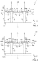
- Figure 1 shows a basic structure of a vertical MOSFET device 1, in lateral view and in a tri-axial reference system of orthogonal axis X, Y, Z.
- the MOSFET device 1 includes a plurality of these basic structures that work together, sharing a same drain terminal (D), with all gate terminals (G) connected together by a deposited polysilicon mesh (not shown), and all of the source terminals (S) electrically connected and linked by a top metal layer 10.
- the MOSFET device 1 comprises a semiconductor body 2, of semiconductor material (which includes a substrate and, optionally, one or more epitaxial layers), having a top surface 2a and a bottom surface 2b.
- the semiconductor body 2 is, e.g., N- doped.
- a drain region 4 is formed, e.g. by implanting dopant species of N-type (N+ doped).
- body regions 5 P doped
- Source regions 8 N+ doped.
- a respective insulating layer 9 covers the gate structures 6.
- the top metal layer 10 electrically contacts the source regions 8 and the body regions 5 at superficial portions 16 and 17 respectively, in order to bias, during use, the source regions 8 and the body regions 5 at a same biasing voltage.
- a P-well region (P+ doped) 14 is formed in some of the body regions 5 and facing the top surface 2a in a region corresponding to the superficial portion 17.
- a silicide interfacing layer (not shown) is formed at the superficial portion 17, to form an ohmic contact between the metal 10 and the implanted P-well region 14.
- the P-well region 14 is formed only where the metal layer 10 is designed to contact the body regions 5.
- the P-well region 14 is arranged between source regions 8, in a respective body region 5.
- the respective source region 8 extends continuously within the body region 5 which houses it, facing the top surface 2a at the superficial region 16. Further layers, to enhance the electrical contact between the metal 10 and the source 8 may be formed, in a per se known way and not shown.
- the PN junction is not a "perfect diode".
- the diode is the collector-base junction of a Bipolar Junction Transistor (BJT), also called the parasitic transistor, made by the N+ source 8, P/P+ body 5, and N+ drain 4, with the base shorted to the emitter by the metal layer 10.
- BJT Bipolar Junction Transistor
- the behavior of the same in failure mode at the short circuit event should be taken into account, where the simultaneous presence of high current and high voltage produces a thermal runaway, leading to the destruction of the device (e.g., typical case of event that occurs when an electric motor halts).
- silicon carbide As is known, some semiconductor materials are ideal for producing electronic components, such as diodes or transistors, in particular for power applications. These materials have wide forbidden band gap, in particular, have an energy value Eg of the forbidden band gap greater than 1.1 eV, low on-state resistance (R ON ), high value of thermal conductivity, high operating frequency, and high velocity saturation of charge carriers.
- a material having said characteristics, and designed to be used for manufacturing electronic components is silicon carbide (SiC).
- SiC silicon carbide
- silicon carbide in its different polytypes (e.g., 3C-SiC, 4H-SiC, 6H-SiC), is preferable to silicon as regards the properties listed previously.
- Electronic devices provided on a silicon-carbide substrate as compared to similar devices provided on a silicon substrate, present numerous advantageous characteristics, such as low output resistance in conduction, low leakage current, high working temperature, and high working frequencies.
- the resistance in ON-state is furthermore impacted, since the source resistance depends upon the doping value of the source region 8.
- the aim of the present invention is to provide an electronic device and a manufacturing method thereof, that overcome the drawbacks of the prior art.
- the aim of the present invention is to limit the thermal runaway, proposing a method that limits the saturation current and the power dissipated locally, with minimum impact on the output resistance of the device.
- an electronic device and a manufacturing method thereof are provided, as defined in the annexed claims.
- Figure 2 shows a portion of MOSFET device 100 according to an embodiment of the present invention.
- Figure 2 is a lateral cross-section view, in the same tri-axial reference system of orthogonal axis X, Y, Z of Figure 1 .
- the portion shown in Figure 2 may be a basic structure, or "cell”, that may be used to develop a MOSFET device 100 by replicating the basic structure a desired number of times; such basic structures work together, sharing a common drain terminal (D), a common gate terminal (G), and a common source terminal (S).
- D drain terminal
- G gate terminal
- S common source terminal
- the MOSFET device 100 comprises a semiconductor body 102, of semiconductor material (which includes, for example, a substrate and, optionally, one or more epitaxial layers), having a top surface 102a and a bottom surface 102b opposite to one another along axis Z.
- semiconductor material which includes, for example, a substrate and, optionally, one or more epitaxial layers
- the semiconductor body 102 is made of silicon carbide (SiC), more in particular 4H-SiC.
- the semiconductor body 102 is, in one embodiment, N- doped.
- a drain region 104 Facing the bottom surface 102b is a drain region 104, e.g. formed by implanted dopant species of N-type (N+ doped) .
- Body regions 105 are arranged at the top surface 102a.
- Source regions 108 are formed by implantation in the semiconductor body 102, within the body regions 105, facing the top surface 102a. Therefore, the body regions 105 surround respective source regions 108 formed therein.
- Gate structures 106 extend on the top surface 102a, and include a stack formed by a gate conductive layer 106a (e.g., of metal material) and a gate dielectric layer 106b (of insulating or dielectric material). A respective insulating layer 109 covers each gate structure 106, to electrically insulate the gate structures 106 from the metal layer 110.
- the gate structures 106 overlap in part the source regions 8; a respective channel region 118 is formed, during use, in the region of the semiconductor body 102 below the gate structures 106, between body regions 105/source regions 108, in a per se known way.
- the current path is pictured in Figure 2 with a dashed line 118 and goes from the source regions 108 towards the drain region 104 (vertical conduction).
- the active area of the MOSFET device 100 is the area where current conduction takes place and, in particular, where the channel is formed. Typically, the active area is surrounded, either completely or partially, by an edge termination region, not shown and per se known.
- the edge termination region is, e.g., an implanted region having a P conductivity type.
- all gate structures 106 are electrically connected together (e.g., by a polysilicon mesh), and all of the source regions 108 are electrically connected together.
- the top metal layer 110 is in electrical contact with the source regions 108 and the body regions 105 at respective contact zones, in order to bias, during use, the source regions 108 and the body regions 105 at a same biasing voltage.
- an electrical-contact interface (P+ doped) 114 is formed in one or more body regions 105, at the top surface 2a.
- each electrical-contact interface 114 includes a silicide interfacing layer (not shown), to form an ohmic contact between the top metal layer 110 and the respective electrical-contact interface 114.
- the electrical-contact interface 114 is formed where the metal layer 110 reaches the top surface 102a to contact the body regions 105.
- an electrical-contact interface 116 is also present between the top metal layer 110 and the region of the semiconductor body where, by design, it has been decided to form the contact between the top metal layer 110 and the source regions 108.
- the device 100 presents an implanted region 120 extending in proximity to, or directly facing, the top surface 102a, along the entire extension of the device 100.
- the implanted region 120 is of N-type and has the function of modulating the saturation current of the device 100.
- the saturation current is the maximum current that the device sustains at a given gate voltage Vg and remains almost constant exceeding a certain drain-source voltage V DS (knee voltage) once exceeded the linear region (where the on-state resistance R ON is identified).
- the saturation current value is limited by the switch-on voltage value of the device (Vth): a higher Vth corresponds to a lower saturation current.
- the implanted region 120 is designed so as to present at least a first sub-region 121 having a first N-type dopant value, and at least a second sub-region 123 having a second N-type dopant value, lower than the first value of the first sub-region 121.
- the implanted region 120 extends, facing the top surface 102a, within the body regions 105, the source regions 108, and in the zone below the gate dielectric 106b intended to house the conductive channel and in the drain regions 104.
- the implanted region 120 is in electrical contact with the body regions 105, the source regions 108 and the electrical-contact interfaces 114.
- the depth of the implanted region 120 in the semiconductor body 102 ranges from 10 nm to 0.1 ⁇ m, in particular from 20 nm to 50 nm.
- the threshold voltage Vth is lowered, i.e. the gate-source voltage value V GS necessary to generate, or switch on, the conductive channel with respect to the second sub-region 123, is reduced.
- the threshold voltage Vth is defined as the gate-source voltage V GS at which the drain-source current I DS is equal to 250 ⁇ A/mm 2 .
- the implant By localizing the implant in proximity to the top surface 102a (in particular at the interface between the semiconductor body 102 and the gate dielectric layer 106b) it is possible to influence the threshold voltage Vth in that specific zone of the device 100, as a consequence of the saturation of interface defects typically present in SiC (e.g., as demonstrated by I. Pintilie et al., "Analysis of electron traps at the 4H-SiC/SiO2 interface; influence by nitrogen implantation prior to wet oxidation", Journal of Applied Physics 108, 024503, 2010 ).
- the sub-region 121 switches on with a voltage V GS lower than the voltage V GS required for switching on the sub-region 123.
- V GS increases, a conductive channel is formed first in the sub-region 121 and, subsequently, in the sub-region 123.
- the voltage V GS is such to switch on both the channel in the sub-region 121 and in the sub-region 123, however, a higher current density is observed in the sub-region 121.
- the N-type dopant concentration in the first sub-region 121 is such that it exceeds the surface concentration of the body region 105 by a factor ranging from 5 to 20 times the concentration of the body region 105; the N-type dopant concentration in the second sub-region 123 is such that it exceeds the surface concentration of the body region 105 by a factor ranging from 2 to 10 times the concentration of the body region 105.
- the ratio Vth2/Vth1 between the threshold voltage Vth2 of the sub-region 123 and the threshold voltage Vth1 of the sub-region 121 ranges from 1.1 to 2.5 and is defined by the ratio of dopant concentration present in the two sub-regions.
- zones of the device 100 designed to carry a greater electric current with respect to other zones of the device 100 or, in other words, it is possible to design zones of the device 100 where the carried current is limited, limiting, as a result, the saturation current in these zones.
- Zones dedicated to the carriage of the highest electric current are chosen on the basis of design considerations, selecting them among the most robust device zones or distributing this current uniformly such that there is no excessive concentration in some zones with respect to others.
- Figures 3A and 3B show a portion of a semiconductor wafer limited to the features of the same that are useful to understand the present invention.
- Figures 3A and 3B illustrate exclusively manufacturing steps useful for the formation of the implanted region 120, while remaining process steps for starting and completing the manufacturing of the device 100 are not described or illustrated, as they are not part of the present invention.
- a first unmasked implant of N-type species e.g., Nitrogen or Phosphorus
- This first implant is carried out with implant energy in the range 10-100 keV.
- a protection layer 134 may be formed on the surface 102a in order to obviate any surface damage of the semiconductor body 102 deriving from the implant.
- the implantat step of Figure 3A forms, in particular, the second sub-region 123 described with reference to Figure 2 , and contributes to forming the first sub-region 121.
- a second masked implant of N-type species (for example, Nitrogen or Phosphorus) is carried out, in order to complete the formation of the first sub-region 121.
- N-type species for example, Nitrogen or Phosphorus
- This second implant (shown by means of arrows 136 in Figure 3B ) is carried out with implant energy in the range 10 - 100 keV.
- a mask 137 used for the second implant leaves exposed superficial portions of the semiconductor body 102 corresponding to the regions where only the first sub-region 121 is to be formed.
- the mask 137 may be formed as a hard mask, depositing a mask layer, for example of silicon oxide, on the surface 102a of the semiconductor body 102 and shaping this mask layer to expose the superficial regions of the semiconductor body 102 where it is desired to implant the sub-region 121.
- an annealing step is carried out, to favor the activation of all the implanted species of the sub-regions 121, 123.
- the annealing step is carried out at temperature in the range 1600 - 1800°C. This annealing step may be dedicated for the formation of the implanted region 120, or common to the implanted region 120 and to the body and/or source and/or drain regions.
- Figure 4A illustrates, purely by way of example, a top view of a portion of the device 100 limited to the body regions 105 and to the implants of the first sub-region 121 (as said, the sub-region 123 is considered to be uniformly present at all the surface 102a of the device 100 - not including portions of the surface 102a which do not belong to the device 100).
- a plurality of body regions 105 extend in the form of strips parallel to each other along the Y-axis direction; a plurality of first sub-regions 121 extend in the form of strips parallel to each other along the X-axis direction, overlapping the plurality of body regions 105.
- the first sub-regions 121 may cover a variable percentage of the body regions 105, i.e. cover a percentage ranging from 50% to 80% of the body regions 105.
- Figures 4B-4D illustrate, according to respective embodiments alternative to each other and to that of Figure 4A , respective top views of a portion of the device 100 limited to the body regions 105 and to the implants of the first sub-region 121.
- a plurality of body regions 105 extend in the form of strips parallel to each other along the Y-axis direction, similarly to Figure 4A ;
- a plurality of first sub-regions 121 extend in the form of strips parallel to each other along the same Y-axis direction, partially overlapping the plurality of body regions 105.
- the strips of the first sub-regions 121 may extend completely overlapping respective strips of the body regions 105 as illustrated in Figure 4B , or only partially overlapping them, as illustrated in Figures 4C and 4D .
- Figure 4B (and similarly Figure 4C ) illustrates first sub-regions 121 which extend to cover body regions 105 alternated to each other (one every two, i.e. the total area of the first sub-regions 121 is equal to 50% of the total area of the body regions 105).
- Figure 4C illustrates first sub-regions 121 which extend between strips arranged side by side and directly facing each other of the body regions 105, partially overlapping these body regions 105 arranged side by side.
- the total extension (or area) of the first sub-regions 121 is equal to 50% of the total area of the body regions 105.
- Figure 4D illustrates an implementation of the first "checkerboard" sub-regions 121, where the first sub-regions 121 extend along the body regions 105 discontinuously.
- inventions of the present invention have been found to increase the ruggedness during short-circuit tests.
- structure of Figure 2 (in the various described embodiments) allows to modulate the saturation current of the MOSFET device 100 at selected portions of the device 100, with a minimum impact on the output resistance of the device 100.
- the layout design is carried out so as to eliminate zones with high current density. For example, therefore at wires or clips, the saturation current is limited, to uniform the total current which circulates in the device and to avoid the destruction of the device in case of short circuit.
- the embodiments previously disclosed refer to a N-channel MOSFET.
- the present invention may be applied, as apparent to the skilled person, to a P-channel MOSFET as well.
Landscapes
- Electrodes Of Semiconductors (AREA)
- Insulated Gate Type Field-Effect Transistor (AREA)
- Ceramic Products (AREA)
- Internal Circuitry In Semiconductor Integrated Circuit Devices (AREA)
Abstract
Description
- The present invention relates to an electronic device and a manufacturing method thereof. In particular, the present invention refers to an electronic device provided with selective regions having different conduction threshold voltage or, alternatively, different saturation current.
-
Figure 1 shows a basic structure of avertical MOSFET device 1, in lateral view and in a tri-axial reference system of orthogonal axis X, Y, Z. In a typical embodiment, theMOSFET device 1 includes a plurality of these basic structures that work together, sharing a same drain terminal (D), with all gate terminals (G) connected together by a deposited polysilicon mesh (not shown), and all of the source terminals (S) electrically connected and linked by atop metal layer 10. - As depicted in
Figure 1 , theMOSFET device 1 comprises asemiconductor body 2, of semiconductor material (which includes a substrate and, optionally, one or more epitaxial layers), having atop surface 2a and abottom surface 2b. Thesemiconductor body 2 is, e.g., N- doped. At thebottom surface 2b, a drain region 4 is formed, e.g. by implanting dopant species of N-type (N+ doped). At thetop surface 2a body regions 5 (P doped) surround source regions 8 (N+ doped).Gate structures 6, including a stack formed by a gateconductive layer 6a and a gatedielectric layer 6b, extend on thetop surface 2a, overlapping in part thesource regions 8. A respectiveinsulating layer 9 covers thegate structures 6. - The
top metal layer 10 electrically contacts thesource regions 8 and thebody regions 5 atsuperficial portions source regions 8 and thebody regions 5 at a same biasing voltage. - To improve the electrical contact between the
top metal layer 10 and thebody regions 5, a P-well region (P+ doped) 14 is formed in some of thebody regions 5 and facing thetop surface 2a in a region corresponding to thesuperficial portion 17. Typically, a silicide interfacing layer (not shown) is formed at thesuperficial portion 17, to form an ohmic contact between themetal 10 and the implanted P-well region 14. The P-well region 14 is formed only where themetal layer 10 is designed to contact thebody regions 5. The P-well region 14 is arranged betweensource regions 8, in arespective body region 5. - Where, by design, it has been decided to form the contact between the
top metal layer 10 and the source regions 8 (i.e., at the superficial region 16), therespective source region 8 extends continuously within thebody region 5 which houses it, facing thetop surface 2a at thesuperficial region 16. Further layers, to enhance the electrical contact between themetal 10 and thesource 8 may be formed, in a per se known way and not shown. - During the ON state of the
MOSFET device 1, while gate-source voltage VGS is above threshold, a conduction current is localized in the drain region 4 and in the region of thesemiconductor body 2 below the gate structure 6 (current flow 18). During OFF state of theMOSFET device 1, the voltage drop across the drain D and source S is sustained by a PN junction at reverse bias, and a very small current (leakage) flows through the PN junction. If the voltage increases too much and the electrical field reaches a critical value, the PN junction goes into breakdown, and the current starts to flow through thebody region 5. If an overvoltage is applied to the PN junction, a current flows through it while theMOSFET device 1 limits the actual drain-source breakdown voltage (BVDS). The breakdown mechanism itself is not destructive for a PN junction. However, overheating caused by the high breakdown current and voltage damages the PN junction unless sufficient heat sinking is provided. - Considering the MOSFET structure in greater detail, one may see that the PN junction is not a "perfect diode". The diode is the collector-base junction of a Bipolar Junction Transistor (BJT), also called the parasitic transistor, made by the
N+ source 8, P/P+ body 5, and N+ drain 4, with the base shorted to the emitter by themetal layer 10. - When designing the device, the behavior of the same in failure mode at the short circuit event should be taken into account, where the simultaneous presence of high current and high voltage produces a thermal runaway, leading to the destruction of the device (e.g., typical case of event that occurs when an electric motor halts).
- As is known, some semiconductor materials are ideal for producing electronic components, such as diodes or transistors, in particular for power applications. These materials have wide forbidden band gap, in particular, have an energy value Eg of the forbidden band gap greater than 1.1 eV, low on-state resistance (RON), high value of thermal conductivity, high operating frequency, and high velocity saturation of charge carriers. A material having said characteristics, and designed to be used for manufacturing electronic components, is silicon carbide (SiC). In particular, silicon carbide, in its different polytypes (e.g., 3C-SiC, 4H-SiC, 6H-SiC), is preferable to silicon as regards the properties listed previously.
- Electronic devices provided on a silicon-carbide substrate, as compared to similar devices provided on a silicon substrate, present numerous advantageous characteristics, such as low output resistance in conduction, low leakage current, high working temperature, and high working frequencies.
- However, the above issues are not fully overcome by the use of SiC and, to improve the avalanche capability of the MOSFET device, common solutions foresee an edge structure having a much higher breakdown threshold with respect to the active area. However, due to limitation of efficiency at the edges of the device, this target is not always feasible.
- The resistance in ON-state is furthermore impacted, since the source resistance depends upon the doping value of the
source region 8. - The aim of the present invention is to provide an electronic device and a manufacturing method thereof, that overcome the drawbacks of the prior art. In particular, the aim of the present invention is to limit the thermal runaway, proposing a method that limits the saturation current and the power dissipated locally, with minimum impact on the output resistance of the device.
- According to the present invention, an electronic device and a manufacturing method thereof are provided, as defined in the annexed claims.
- For a better understanding of the present invention, preferred embodiments thereof are now described, purely by way of non-limiting example, with reference to the attached drawings, wherein:
-
Figure 1 shows a MOSFET device of a known type; -
Figure 2 shows a MOSFET device according to an embodiment of the present invention; -
Figures 3A and 3B show process steps to manufacture the MOSFET device ofFigure 2 ; and -
Figures 4A-4D show plan views of respective layouts of implanted regions of the MOSFET device ofFigure 2 , according to respective embodiments of the present invention. -
Figure 2 shows a portion ofMOSFET device 100 according to an embodiment of the present invention.Figure 2 is a lateral cross-section view, in the same tri-axial reference system of orthogonal axis X, Y, Z ofFigure 1 . - As already discussed with reference to
Figure 1 , the portion shown inFigure 2 may be a basic structure, or "cell", that may be used to develop aMOSFET device 100 by replicating the basic structure a desired number of times; such basic structures work together, sharing a common drain terminal (D), a common gate terminal (G), and a common source terminal (S). - It is apparent that, when replicating the portion of
Figure 2 , variations in the basic structure may be introduced, as apparent to the skilled person in the art, for example in order to comply with one or more among design requirements, area occupation, electrical requirements, manufacturing requirements, etc. - The
MOSFET device 100 comprises asemiconductor body 102, of semiconductor material (which includes, for example, a substrate and, optionally, one or more epitaxial layers), having atop surface 102a and abottom surface 102b opposite to one another along axis Z. - In particular, the
semiconductor body 102 is made of silicon carbide (SiC), more in particular 4H-SiC. Thesemiconductor body 102 is, in one embodiment, N- doped. - Facing the
bottom surface 102b is a drain region 104, e.g. formed by implanted dopant species of N-type (N+ doped) . Body regions 105 (P doped) are arranged at thetop surface 102a. - Source regions 108 (N+ doped) are formed by implantation in the
semiconductor body 102, within thebody regions 105, facing thetop surface 102a. Therefore, thebody regions 105 surroundrespective source regions 108 formed therein. -
Gate structures 106 extend on thetop surface 102a, and include a stack formed by a gateconductive layer 106a (e.g., of metal material) and a gatedielectric layer 106b (of insulating or dielectric material). A respectiveinsulating layer 109 covers eachgate structure 106, to electrically insulate thegate structures 106 from themetal layer 110. Thegate structures 106 overlap in part thesource regions 8; arespective channel region 118 is formed, during use, in the region of thesemiconductor body 102 below thegate structures 106, betweenbody regions 105/source regions 108, in a per se known way. The current path is pictured inFigure 2 with adashed line 118 and goes from thesource regions 108 towards the drain region 104 (vertical conduction). - The active area of the
MOSFET device 100 is the area where current conduction takes place and, in particular, where the channel is formed. Typically, the active area is surrounded, either completely or partially, by an edge termination region, not shown and per se known. The edge termination region is, e.g., an implanted region having a P conductivity type. - In a way which is not shown in detail and which is per se known, all
gate structures 106 are electrically connected together (e.g., by a polysilicon mesh), and all of thesource regions 108 are electrically connected together. - The
top metal layer 110 is in electrical contact with thesource regions 108 and thebody regions 105 at respective contact zones, in order to bias, during use, thesource regions 108 and thebody regions 105 at a same biasing voltage. - To improve the electrical contact between the
top metal layer 110 and thebody regions 105, an electrical-contact interface (P+ doped) 114 is formed in one ormore body regions 105, at thetop surface 2a. Typically, each electrical-contact interface 114 includes a silicide interfacing layer (not shown), to form an ohmic contact between thetop metal layer 110 and the respective electrical-contact interface 114. The electrical-contact interface 114 is formed where themetal layer 110 reaches thetop surface 102a to contact thebody regions 105. - According to an aspect of the present invention, an electrical-
contact interface 116 is also present between thetop metal layer 110 and the region of the semiconductor body where, by design, it has been decided to form the contact between thetop metal layer 110 and thesource regions 108. - According to an aspect of the present invention, the
device 100 presents an implantedregion 120 extending in proximity to, or directly facing, thetop surface 102a, along the entire extension of thedevice 100. The implantedregion 120 is of N-type and has the function of modulating the saturation current of thedevice 100. In this context, the saturation current is the maximum current that the device sustains at a given gate voltage Vg and remains almost constant exceeding a certain drain-source voltage VDS (knee voltage) once exceeded the linear region (where the on-state resistance RON is identified). The saturation current value is limited by the switch-on voltage value of the device (Vth): a higher Vth corresponds to a lower saturation current. - The implanted
region 120 is designed so as to present at least afirst sub-region 121 having a first N-type dopant value, and at least asecond sub-region 123 having a second N-type dopant value, lower than the first value of thefirst sub-region 121. - The implanted
region 120 extends, facing thetop surface 102a, within thebody regions 105, thesource regions 108, and in the zone below thegate dielectric 106b intended to house the conductive channel and in the drain regions 104. - Therefore, the implanted
region 120 is in electrical contact with thebody regions 105, thesource regions 108 and the electrical-contact interfaces 114. - The depth of the implanted
region 120 in thesemiconductor body 102, measured from thetop surface 102a along the Z direction, ranges from 10 nm to 0.1 µm, in particular from 20 nm to 50 nm. - Where the implant dose is increased (first sub-region 121), the threshold voltage Vth is lowered, i.e. the gate-source voltage value VGS necessary to generate, or switch on, the conductive channel with respect to the
second sub-region 123, is reduced. The threshold voltage Vth is defined as the gate-source voltage VGS at which the drain-source current IDS is equal to 250 µA/mm2. - By localizing the implant in proximity to the
top surface 102a (in particular at the interface between thesemiconductor body 102 and thegate dielectric layer 106b) it is possible to influence the threshold voltage Vth in that specific zone of thedevice 100, as a consequence of the saturation of interface defects typically present in SiC (e.g., as demonstrated by I. Pintilie et al., "Analysis of electron traps at the 4H-SiC/SiO2 interface; influence by nitrogen implantation prior to wet oxidation", Journal of ). - In this manner, during operation, the
sub-region 121, having higher dopant density, switches on with a voltage VGS lower than the voltage VGS required for switching on thesub-region 123. As a result, as the voltage VGS increases, a conductive channel is formed first in thesub-region 121 and, subsequently, in thesub-region 123. Furthermore, when the voltage VGS is such to switch on both the channel in thesub-region 121 and in thesub-region 123, however, a higher current density is observed in thesub-region 121. - The N-type dopant concentration in the
first sub-region 121 is such that it exceeds the surface concentration of thebody region 105 by a factor ranging from 5 to 20 times the concentration of thebody region 105; the N-type dopant concentration in thesecond sub-region 123 is such that it exceeds the surface concentration of thebody region 105 by a factor ranging from 2 to 10 times the concentration of thebody region 105. - The ratio Vth2/Vth1 between the threshold voltage Vth2 of the
sub-region 123 and the threshold voltage Vth1 of thesub-region 121 ranges from 1.1 to 2.5 and is defined by the ratio of dopant concentration present in the two sub-regions. - Thus, with an appropriate layout of the implanted
region 120, it is possible to define zones of thedevice 100 designed to carry a greater electric current with respect to other zones of thedevice 100 or, in other words, it is possible to design zones of thedevice 100 where the carried current is limited, limiting, as a result, the saturation current in these zones. Zones dedicated to the carriage of the highest electric current are chosen on the basis of design considerations, selecting them among the most robust device zones or distributing this current uniformly such that there is no excessive concentration in some zones with respect to others. - As to the manufacturing process of the implanted
region 120, reference is made toFigures 3A and 3B , which show a portion of a semiconductor wafer limited to the features of the same that are useful to understand the present invention.Figures 3A and 3B illustrate exclusively manufacturing steps useful for the formation of the implantedregion 120, while remaining process steps for starting and completing the manufacturing of thedevice 100 are not described or illustrated, as they are not part of the present invention. - With reference to
Figure 3A , after having formed thebody regions 105 through an implant of P doping species, and thesource regions 108 through an implant of N doping species, a first unmasked implant of N-type species (e.g., Nitrogen or Phosphorus) is carried out, in order to form a first implantedregion 130 in theinterface 102a. This first implant (shown by means of arrows inFigure 3A ) is carried out with implant energy in the range 10-100 keV. A protection layer 134 may be formed on thesurface 102a in order to obviate any surface damage of thesemiconductor body 102 deriving from the implant. - The implantat step of
Figure 3A forms, in particular, thesecond sub-region 123 described with reference toFigure 2 , and contributes to forming thefirst sub-region 121. - Then,
Figure 3B , a second masked implant of N-type species (for example, Nitrogen or Phosphorus) is carried out, in order to complete the formation of thefirst sub-region 121. - This second implant (shown by means of
arrows 136 inFigure 3B ) is carried out with implant energy in the range 10 - 100 keV. Amask 137 used for the second implant leaves exposed superficial portions of thesemiconductor body 102 corresponding to the regions where only thefirst sub-region 121 is to be formed. In one embodiment, themask 137 may be formed as a hard mask, depositing a mask layer, for example of silicon oxide, on thesurface 102a of thesemiconductor body 102 and shaping this mask layer to expose the superficial regions of thesemiconductor body 102 where it is desired to implant thesub-region 121. - Then, an annealing step is carried out, to favor the activation of all the implanted species of the
sub-regions region 120, or common to the implantedregion 120 and to the body and/or source and/or drain regions. -
Figure 4A illustrates, purely by way of example, a top view of a portion of thedevice 100 limited to thebody regions 105 and to the implants of the first sub-region 121 (as said, thesub-region 123 is considered to be uniformly present at all thesurface 102a of the device 100 - not including portions of thesurface 102a which do not belong to the device 100). As is noted, in this embodiment, a plurality ofbody regions 105 extend in the form of strips parallel to each other along the Y-axis direction; a plurality offirst sub-regions 121 extend in the form of strips parallel to each other along the X-axis direction, overlapping the plurality ofbody regions 105. At designer's choice, thefirst sub-regions 121 may cover a variable percentage of thebody regions 105, i.e. cover a percentage ranging from 50% to 80% of thebody regions 105. -
Figures 4B-4D illustrate, according to respective embodiments alternative to each other and to that ofFigure 4A , respective top views of a portion of thedevice 100 limited to thebody regions 105 and to the implants of thefirst sub-region 121. As is noted, in these embodiments, a plurality ofbody regions 105 extend in the form of strips parallel to each other along the Y-axis direction, similarly toFigure 4A ; a plurality offirst sub-regions 121 extend in the form of strips parallel to each other along the same Y-axis direction, partially overlapping the plurality ofbody regions 105. - The strips of the
first sub-regions 121 may extend completely overlapping respective strips of thebody regions 105 as illustrated inFigure 4B , or only partially overlapping them, as illustrated inFigures 4C and 4D . -
Figure 4B (and similarlyFigure 4C ) illustratesfirst sub-regions 121 which extend to coverbody regions 105 alternated to each other (one every two, i.e. the total area of thefirst sub-regions 121 is equal to 50% of the total area of the body regions 105). -
Figure 4C illustratesfirst sub-regions 121 which extend between strips arranged side by side and directly facing each other of thebody regions 105, partially overlapping thesebody regions 105 arranged side by side. As forFigure 4B , the total extension (or area) of thefirst sub-regions 121 is equal to 50% of the total area of thebody regions 105. -
Figure 4D illustrates an implementation of the first "checkerboard"sub-regions 121, where thefirst sub-regions 121 extend along thebody regions 105 discontinuously. - From what has been described, the advantages that the invention achieves are apparent.
- The embodiments of the present invention have been found to increase the ruggedness during short-circuit tests. In fact, the structure of
Figure 2 (in the various described embodiments) allows to modulate the saturation current of theMOSFET device 100 at selected portions of thedevice 100, with a minimum impact on the output resistance of thedevice 100. - The layout design is carried out so as to eliminate zones with high current density. For example, therefore at wires or clips, the saturation current is limited, to uniform the total current which circulates in the device and to avoid the destruction of the device in case of short circuit.
- Finally, it is clear that modifications and variations may be made to what has been described and illustrated herein, without thereby departing from the scope of the present invention, as defined in the annexed claims.
- For example, the embodiments previously disclosed refer to a N-channel MOSFET. However, the present invention may be applied, as apparent to the skilled person, to a P-channel MOSFET as well.
Claims (17)
- An electronic device (100) comprising:a semiconductor body (102) of silicon carbide, SiC, having a first (102a) and a second surface (102b), opposite to one another along a direction (Z);a body region (105), having a first conductivity (P), extending in the semiconductor body (102) at the first surface (102a);a source region (108), having a second conductivity (N) opposite to the first conductivity (P), extending in the body region (105) at the first surface (102a) of the semiconductor body (102); anda drain region (104), having the second conductivity (N), extending at the second surface (102b) of the semiconductor body (102),characterized in that it further comprises a doped region (120), having the second conductivity (N), extending continuously at the entire first surface (102a) of the semiconductor body (102), and including one or more first sub-regions (121) having a first doping density and one or more second sub-regions (123) having a second doping density lower than the first doping density.
- The device according to claim 1, wherein the first sub-regions (121) are alternated with the second sub-regions (123) so to form zones alternated to each other having different conduction threshold voltage (Vth1, Vth2) or, alternatively, different saturation current.
- The device according to claim 1 or 2, wherein each first sub-region (121) and each second sub-region (123) is designed in such a way that the ratio (Vth2/Vth1) between a conduction threshold voltage (Vth2) of each second sub-region (123) and a conduction threshold voltage (Vth1) of each first sub-region (121) ranges from 1.1 to 2.5.
- The device according to anyone of the preceding claims, wherein the first and the second sub-regions (121, 123) have a depth, in said semiconductor body from the surface (102a) ranging from 10 nm to 0.1 pm.
- The device according to anyone of the preceding claims, wherein the first doping density has a value ranging from 5 to 20 times a respective doping density value of the body region (105) and the second doping density has a respective value ranging from 2 to 10 times the doping density value of the body region (105).
- The device according to anyone of the preceding claims, wherein said first sub-regions (121) are contiguous to, and electrically connected to, respective second sub-regions (123).
- The device according to anyone of the preceding claims, wherein the second sub-regions (123) occupy a volume of the doped region (120) ranging from 50% to 80%.
- The device according to anyone of the preceding claims, further comprising a gate structure (106) on the first surface (102a) of the semiconductor body including: a gate dielectric layer (106b), a metal gate layer (106a) on the gate dielectric layer (106b), and an insulating layer surrounding the metal gate layer (106a),
said doped region (120) extending within the source regions, the body regions and below said gate structure (106) . - The device according to anyone of the preceding claims, wherein said semiconductor body (102) is of 4H-SiC.
- A method for manufacturing an electronic device (100), comprising the steps of:arranging a semiconductor body (102) of silicon carbide, SiC, having a first (102a) and a second surface (102b), opposite to one another along a direction (Z);forming a body region (105), having a first conductivity (P), in the semiconductor body (102) at the first surface (102a);forming a source region (108), having a second conductivity (N) opposite to the first conductivity (P), in the body region (105) at the first surface (102a) of the semiconductor body (102); andforming a drain region (104), having the second conductivity (N), at the second surface (102b),characterized in that it further comprises the step of forming a doped region (120), having the second conductivity (N), extending seamlessly at the entire first surface (102a) of the semiconductor body (102), including the sub-steps of:forming one or more first sub-regions (121) having a first doping density; andforming one or more second sub-regions (123) having a second doping density lower than the first doping density.
- The method according to claim 10, wherein the first sub-regions (121) are alternated with the second sub-regions (123) so to form zones alternated to each other having different conduction threshold voltage (Vth1, Vth2) or, alternatively, different saturation current.
- The method according to claim 10 or 11, wherein each first sub-region (121) and each second sub-region (123) is designed in such a way that the ratio (Vth2/Vth1) between a conduction threshold voltage (Vth2) of each second sub-region (123) and a conduction threshold voltage (Vth1) of each first sub-region (121) ranges from 1.1 to 2.5.
- The method according to anyone of claims 10-12, wherein the first and the second sub-regions (121, 123) have a depth, in said semiconductor body from the surface (102a) ranging from 10 nm to 0.1 µm.
- The method according to anyone of claims 10-13, wherein forming said doped region (120) comprises the steps of:carrying out an unmasked implant at the entire first surface (102a), thus forming a uniformly doped region having the second doping density;arranging an implant mask (137) on the first surface (102a), said implant mask (137) exposing superficial regions of the semiconductor body (102) at which it is desired to form the first sub-regions (121);carrying out a masked implant, using said implant mask (137), to form selectively doped regions having the first doping concentration.
- The method according to claim 14, wherein the first doping density has a value ranging from 5 to 20 times a respective doping density value of the body region (105) and the second doping density has a respective value ranging from 2 to 10 times the doping density value of the body region (105).
- The method according to anyone of claims 10-15, wherein said first sub-regions (121) are contiguous to, and electrically connected to, respective second sub-regions (123) .
- The method according to anyone of the preceding claims, wherein the second sub-regions (123) occupy a volume of the doped region (120) ranging from 50% to 80%.
Applications Claiming Priority (1)
| Application Number | Priority Date | Filing Date | Title |
|---|---|---|---|
| IT102020000015076A IT202000015076A1 (en) | 2020-06-23 | 2020-06-23 | ELECTRONIC DEVICE IN 4H-SIC WITH IMPROVED SHORT-CIRCUIT PERFORMANCE, AND RELATED MANUFACTURING METHOD |
Publications (1)
| Publication Number | Publication Date |
|---|---|
| EP3930007A1 true EP3930007A1 (en) | 2021-12-29 |
Family
ID=72473754
Family Applications (1)
| Application Number | Title | Priority Date | Filing Date |
|---|---|---|---|
| EP21180931.4A Pending EP3930007A1 (en) | 2020-06-23 | 2021-06-22 | 4h-sic electronic device with improved short-circuit performances, and manufacturing method thereof |
Country Status (4)
| Country | Link |
|---|---|
| US (1) | US11798981B2 (en) |
| EP (1) | EP3930007A1 (en) |
| JP (2) | JP7776941B2 (en) |
| IT (1) | IT202000015076A1 (en) |
Families Citing this family (3)
| Publication number | Priority date | Publication date | Assignee | Title |
|---|---|---|---|---|
| US11728422B2 (en) | 2019-11-14 | 2023-08-15 | Stmicroelectronics S.R.L. | Power MOSFET device having improved safe-operating area and on resistance, manufacturing process thereof and operating method thereof |
| CN215680697U (en) * | 2020-06-23 | 2022-01-28 | 意法半导体股份有限公司 | Electronic device and semiconductor device |
| CN116013905B (en) * | 2023-03-27 | 2023-06-23 | 通威微电子有限公司 | A kind of semiconductor device and its manufacturing method |
Citations (4)
| Publication number | Priority date | Publication date | Assignee | Title |
|---|---|---|---|---|
| US6573534B1 (en) * | 1995-09-06 | 2003-06-03 | Denso Corporation | Silicon carbide semiconductor device |
| JP4532853B2 (en) * | 2003-06-13 | 2010-08-25 | パナソニック株式会社 | Semiconductor device |
| US20120205739A1 (en) * | 2009-10-22 | 2012-08-16 | Panasonic Corporation | Semiconductor device and process for production thereof |
| WO2019123601A1 (en) * | 2017-12-21 | 2019-06-27 | 三菱電機株式会社 | Semiconductor device |
Family Cites Families (51)
| Publication number | Priority date | Publication date | Assignee | Title |
|---|---|---|---|---|
| US4374455A (en) | 1979-10-30 | 1983-02-22 | Rca Corporation | Method for manufacturing a vertical, grooved MOSFET |
| US4672407A (en) | 1984-05-30 | 1987-06-09 | Kabushiki Kaisha Toshiba | Conductivity modulated MOSFET |
| US5528058A (en) | 1986-03-21 | 1996-06-18 | Advanced Power Technology, Inc. | IGBT device with platinum lifetime control and reduced gaw |
| US4931408A (en) | 1989-10-13 | 1990-06-05 | Siliconix Incorporated | Method of fabricating a short-channel low voltage DMOS transistor |
| US5817546A (en) | 1994-06-23 | 1998-10-06 | Stmicroelectronics S.R.L. | Process of making a MOS-technology power device |
| JP3385938B2 (en) * | 1997-03-05 | 2003-03-10 | 株式会社デンソー | Silicon carbide semiconductor device and method of manufacturing the same |
| EP0772241B1 (en) | 1995-10-30 | 2004-06-09 | STMicroelectronics S.r.l. | High density MOS technology power device |
| US6228719B1 (en) | 1995-11-06 | 2001-05-08 | Stmicroelectronics S.R.L. | MOS technology power device with low output resistance and low capacitance, and related manufacturing process |
| KR100206555B1 (en) | 1995-12-30 | 1999-07-01 | 윤종용 | Power transistor |
| US5998834A (en) | 1996-05-22 | 1999-12-07 | Siliconix Incorporated | Long channel trench-gated power MOSFET having fully depleted body region |
| JP3077631B2 (en) * | 1997-06-06 | 2000-08-14 | 日本電気株式会社 | MOS semiconductor device for power drive with overheat protection function |
| US6114726A (en) | 1998-03-11 | 2000-09-05 | International Rectifier Corp. | Low voltage MOSFET |
| US7084456B2 (en) | 1999-05-25 | 2006-08-01 | Advanced Analogic Technologies, Inc. | Trench MOSFET with recessed clamping diode using graded doping |
| US6710403B2 (en) | 2002-07-30 | 2004-03-23 | Fairchild Semiconductor Corporation | Dual trench power MOSFET |
| US6853033B2 (en) | 2001-06-05 | 2005-02-08 | National University Of Singapore | Power MOSFET having enhanced breakdown voltage |
| JP3090132U (en) * | 2002-05-21 | 2002-11-29 | 船井電機株式会社 | MOS transistor and switching power supply |
| JP2004104003A (en) | 2002-09-12 | 2004-04-02 | Renesas Technology Corp | Semiconductor element |
| DE10250175B4 (en) | 2002-10-28 | 2005-02-17 | Infineon Technologies Ag | power transistor |
| GB0426412D0 (en) | 2004-12-02 | 2005-01-05 | Koninkl Philips Electronics Nv | Insulated gate field effect transistors |
| EP1791173A1 (en) | 2005-11-25 | 2007-05-30 | STMicroelectronics S.r.l. | Process for manufacturing a MOSFET and corresponding MOSFET |
| JP5048273B2 (en) | 2006-05-10 | 2012-10-17 | オンセミコンダクター・トレーディング・リミテッド | Insulated gate semiconductor device |
| US7598567B2 (en) * | 2006-11-03 | 2009-10-06 | Cree, Inc. | Power switching semiconductor devices including rectifying junction-shunts |
| WO2009050871A1 (en) | 2007-10-15 | 2009-04-23 | Panasonic Corporation | Semiconductor device and method for manufacturing the same |
| DE112009004595B4 (en) | 2009-03-24 | 2015-04-09 | Toyota Jidosha Kabushiki Kaisha | Semiconductor device |
| US8362557B2 (en) | 2009-12-02 | 2013-01-29 | Fairchild Semiconductor Corporation | Stepped-source LDMOS architecture |
| IT1401754B1 (en) | 2010-08-30 | 2013-08-02 | St Microelectronics Srl | INTEGRATED ELECTRONIC DEVICE AND ITS MANUFACTURING METHOD. |
| JP2012064873A (en) | 2010-09-17 | 2012-03-29 | Rohm Co Ltd | Semiconductor device and method of manufacturing the same |
| CN102668094B (en) * | 2010-10-29 | 2015-02-25 | 松下电器产业株式会社 | Semiconductor element and semiconductor device |
| IT1402879B1 (en) | 2010-11-19 | 2013-09-27 | St Microelectronics Srl | IGBT DEVICE WITH REGULATIONS OF BURIED EMITTERS |
| JP2013258333A (en) | 2012-06-13 | 2013-12-26 | Toshiba Corp | Power semiconductor device |
| ITTO20120742A1 (en) | 2012-08-24 | 2014-02-25 | St Microelectronics Srl | SEMICONDUCTOR DEVICE WITH IMPROVED LINEAR AND SWITCHING OPERATING MODES, METHOD OF MANUFACTURING THE SEMICONDUCTOR DEVICE, AND METHOD OF POLARIZATION OF THE SEMICONDUCTOR DEVICE |
| US9530844B2 (en) | 2012-12-28 | 2016-12-27 | Cree, Inc. | Transistor structures having reduced electrical field at the gate oxide and methods for making same |
| WO2014132582A1 (en) | 2013-02-28 | 2014-09-04 | 三菱電機株式会社 | Semiconductor device |
| US9224861B2 (en) | 2013-05-09 | 2015-12-29 | Freescale Semiconductor, Inc. | Semiconductor device with notched gate |
| DE102014111140B4 (en) | 2014-08-05 | 2019-08-14 | Infineon Technologies Austria Ag | Semiconductor device with field effect structures with different gate materials and method for the production thereof |
| US10186573B2 (en) | 2015-09-14 | 2019-01-22 | Maxpower Semiconductor, Inc. | Lateral power MOSFET with non-horizontal RESURF structure |
| US9837358B2 (en) | 2015-10-01 | 2017-12-05 | D3 Semiconductor LLC | Source-gate region architecture in a vertical power semiconductor device |
| JP6690198B2 (en) | 2015-11-16 | 2020-04-28 | 富士電機株式会社 | Method for manufacturing silicon carbide semiconductor device |
| DE102015121100B4 (en) | 2015-12-03 | 2022-01-20 | Infineon Technologies Ag | SEMICONDUCTOR DEVICE WITH TRENCH EDGE TERMINATION |
| JP2017168666A (en) | 2016-03-16 | 2017-09-21 | 株式会社東芝 | Semiconductor device |
| JP6726505B2 (en) | 2016-03-31 | 2020-07-22 | ローム株式会社 | Method of manufacturing semiconductor device |
| US9947787B2 (en) | 2016-05-06 | 2018-04-17 | Silicet, LLC | Devices and methods for a power transistor having a schottky or schottky-like contact |
| JP6574744B2 (en) | 2016-09-16 | 2019-09-11 | 株式会社東芝 | Semiconductor device |
| JP6728096B2 (en) | 2017-04-24 | 2020-07-22 | 株式会社東芝 | Semiconductor device, method of manufacturing semiconductor device, inverter circuit, drive device, vehicle, and elevator |
| CN110718452B (en) | 2018-07-12 | 2025-04-08 | 创能动力科技有限公司 | Silicon carbide device and method for manufacturing same |
| JP7529429B2 (en) | 2019-05-30 | 2024-08-06 | ローム株式会社 | Semiconductor Device |
| DE102019119020B4 (en) | 2019-07-12 | 2026-01-08 | Infineon Technologies Ag | SILICON CARBIDE DEVICE WITH COMPENSATION LAYER AND METHOD FOR MANUFACTURING IT |
| US10950695B1 (en) | 2019-11-05 | 2021-03-16 | Semiq Incorporated | Silicon carbide planar MOSFET with wave-shaped channel regions |
| US11728422B2 (en) | 2019-11-14 | 2023-08-15 | Stmicroelectronics S.R.L. | Power MOSFET device having improved safe-operating area and on resistance, manufacturing process thereof and operating method thereof |
| US10910478B1 (en) | 2020-03-04 | 2021-02-02 | Shuming Xu | Metal-oxide-semiconductor field-effect transistor having enhanced high-frequency performance |
| GB2607292B (en) | 2021-05-31 | 2023-08-30 | Mqsemi Ag | Semiconductor device |
-
2020
- 2020-06-23 IT IT102020000015076A patent/IT202000015076A1/en unknown
-
2021
- 2021-06-02 JP JP2021093095A patent/JP7776941B2/en active Active
- 2021-06-14 US US17/346,771 patent/US11798981B2/en active Active
- 2021-06-22 EP EP21180931.4A patent/EP3930007A1/en active Pending
-
2025
- 2025-11-14 JP JP2025195376A patent/JP2026027463A/en active Pending
Patent Citations (4)
| Publication number | Priority date | Publication date | Assignee | Title |
|---|---|---|---|---|
| US6573534B1 (en) * | 1995-09-06 | 2003-06-03 | Denso Corporation | Silicon carbide semiconductor device |
| JP4532853B2 (en) * | 2003-06-13 | 2010-08-25 | パナソニック株式会社 | Semiconductor device |
| US20120205739A1 (en) * | 2009-10-22 | 2012-08-16 | Panasonic Corporation | Semiconductor device and process for production thereof |
| WO2019123601A1 (en) * | 2017-12-21 | 2019-06-27 | 三菱電機株式会社 | Semiconductor device |
Non-Patent Citations (1)
| Title |
|---|
| I. PINTILIE ET AL.: "Analysis of electron traps at the 4H-SiC/Si0 interface; influence by nitrogen implantation prior to wet oxidation", JOURNAL OF APPLIED PHYSICS, vol. 108, 2010, pages 024503 |
Also Published As
| Publication number | Publication date |
|---|---|
| US20210399089A1 (en) | 2021-12-23 |
| US11798981B2 (en) | 2023-10-24 |
| IT202000015076A1 (en) | 2021-12-23 |
| JP2026027463A (en) | 2026-02-18 |
| JP7776941B2 (en) | 2025-11-27 |
| JP2022003683A (en) | 2022-01-11 |
Similar Documents
| Publication | Publication Date | Title |
|---|---|---|
| US9035375B2 (en) | Field-effect device and manufacturing method thereof | |
| EP2497116B1 (en) | Power semiconductor devices having selectively doped jfet regions and related methods of forming such devices | |
| JP2024511552A (en) | Trench power devices with improved reliability and continuity | |
| US8471333B2 (en) | Semiconductor device and manufacturing method of the same | |
| US11798981B2 (en) | 4H—SiC electronic device with improved short-circuit performances, and manufacturing method thereof | |
| JP7127389B2 (en) | Silicon carbide semiconductor device | |
| KR101530582B1 (en) | Semiconductor device and manufacturing method thereof | |
| CN117096190A (en) | Power switching device with high DV/DT capability and method of making such device | |
| JP2003218348A (en) | Double diffused MOSFET and semiconductor device using the same | |
| JP2016519428A (en) | SiC power vertical DMOS with expanded safe operating area | |
| US20250280573A1 (en) | 4h-sic electronic device with improved short-circuit performances, and manufacturing method thereof | |
| CN114823846A (en) | Guard ring for coupling of edge termination | |
| Zhu et al. | Implementation of high-side, high-voltage RESURF LDMOS in a sub-half micron smart power technology | |
| US12550366B2 (en) | Rugged LDMOS with reduced NSD in source | |
| US20220344467A1 (en) | 4h-sic mosfet device and manufacturing method thereof | |
| CN121986570A (en) | Gate trench power semiconductor devices with shaped deep support shields that reduce cell pitch and on-state resistance | |
| WO1997036329A1 (en) | Insulated gate bipolar transistor having a trench and a method for production thereof | |
| JP2017152579A (en) | Semiconductor device | |
| EP0890191A1 (en) | Insulated gate bipolar transistor having a trench and a method for production thereof |
Legal Events
| Date | Code | Title | Description |
|---|---|---|---|
| PUAI | Public reference made under article 153(3) epc to a published international application that has entered the european phase |
Free format text: ORIGINAL CODE: 0009012 |
|
| STAA | Information on the status of an ep patent application or granted ep patent |
Free format text: STATUS: THE APPLICATION HAS BEEN PUBLISHED |
|
| AK | Designated contracting states |
Kind code of ref document: A1 Designated state(s): AL AT BE BG CH CY CZ DE DK EE ES FI FR GB GR HR HU IE IS IT LI LT LU LV MC MK MT NL NO PL PT RO RS SE SI SK SM TR |
|
| B565 | Issuance of search results under rule 164(2) epc |
Effective date: 20211019 |
|
| STAA | Information on the status of an ep patent application or granted ep patent |
Free format text: STATUS: REQUEST FOR EXAMINATION WAS MADE |
|
| 17P | Request for examination filed |
Effective date: 20220512 |
|
| RBV | Designated contracting states (corrected) |
Designated state(s): AL AT BE BG CH CY CZ DE DK EE ES FI FR GB GR HR HU IE IS IT LI LT LU LV MC MK MT NL NO PL PT RO RS SE SI SK SM TR |
|
| STAA | Information on the status of an ep patent application or granted ep patent |
Free format text: STATUS: EXAMINATION IS IN PROGRESS |
|
| 17Q | First examination report despatched |
Effective date: 20231009 |