EP3929983A1 - Memory and forming method therefor - Google Patents
Memory and forming method therefor Download PDFInfo
- Publication number
- EP3929983A1 EP3929983A1 EP21762995.5A EP21762995A EP3929983A1 EP 3929983 A1 EP3929983 A1 EP 3929983A1 EP 21762995 A EP21762995 A EP 21762995A EP 3929983 A1 EP3929983 A1 EP 3929983A1
- Authority
- EP
- European Patent Office
- Prior art keywords
- word line
- partial
- partial word
- trench
- active regions
- Prior art date
- Legal status (The legal status is an assumption and is not a legal conclusion. Google has not performed a legal analysis and makes no representation as to the accuracy of the status listed.)
- Granted
Links
Images



Classifications
-
- H—ELECTRICITY
- H10—SEMICONDUCTOR DEVICES; ELECTRIC SOLID-STATE DEVICES NOT OTHERWISE PROVIDED FOR
- H10B—ELECTRONIC MEMORY DEVICES
- H10B12/00—Dynamic random access memory [DRAM] devices
- H10B12/30—DRAM devices comprising one-transistor - one-capacitor [1T-1C] memory cells
-
- H—ELECTRICITY
- H10—SEMICONDUCTOR DEVICES; ELECTRIC SOLID-STATE DEVICES NOT OTHERWISE PROVIDED FOR
- H10D—INORGANIC ELECTRIC SEMICONDUCTOR DEVICES
- H10D64/00—Electrodes of devices having potential barriers
- H10D64/01—Manufacture or treatment
- H10D64/025—Manufacture or treatment forming recessed gates, e.g. by using local oxidation
- H10D64/027—Manufacture or treatment forming recessed gates, e.g. by using local oxidation by etching at gate locations
-
- H—ELECTRICITY
- H10—SEMICONDUCTOR DEVICES; ELECTRIC SOLID-STATE DEVICES NOT OTHERWISE PROVIDED FOR
- H10B—ELECTRONIC MEMORY DEVICES
- H10B12/00—Dynamic random access memory [DRAM] devices
- H10B12/01—Manufacture or treatment
- H10B12/02—Manufacture or treatment for one transistor one-capacitor [1T-1C] memory cells
- H10B12/05—Making the transistor
- H10B12/053—Making the transistor the transistor being at least partially in a trench in the substrate
-
- H—ELECTRICITY
- H10—SEMICONDUCTOR DEVICES; ELECTRIC SOLID-STATE DEVICES NOT OTHERWISE PROVIDED FOR
- H10B—ELECTRONIC MEMORY DEVICES
- H10B12/00—Dynamic random access memory [DRAM] devices
- H10B12/30—DRAM devices comprising one-transistor - one-capacitor [1T-1C] memory cells
- H10B12/34—DRAM devices comprising one-transistor - one-capacitor [1T-1C] memory cells the transistor being at least partially in a trench in the substrate
-
- H—ELECTRICITY
- H10—SEMICONDUCTOR DEVICES; ELECTRIC SOLID-STATE DEVICES NOT OTHERWISE PROVIDED FOR
- H10B—ELECTRONIC MEMORY DEVICES
- H10B12/00—Dynamic random access memory [DRAM] devices
- H10B12/30—DRAM devices comprising one-transistor - one-capacitor [1T-1C] memory cells
- H10B12/48—Data lines or contacts therefor
- H10B12/488—Word lines
-
- H—ELECTRICITY
- H10—SEMICONDUCTOR DEVICES; ELECTRIC SOLID-STATE DEVICES NOT OTHERWISE PROVIDED FOR
- H10D—INORGANIC ELECTRIC SEMICONDUCTOR DEVICES
- H10D30/00—Field-effect transistors [FET]
- H10D30/01—Manufacture or treatment
- H10D30/021—Manufacture or treatment of FETs having insulated gates [IGFET]
- H10D30/028—Manufacture or treatment of FETs having insulated gates [IGFET] of double-diffused metal oxide semiconductor [DMOS] FETs
- H10D30/0291—Manufacture or treatment of FETs having insulated gates [IGFET] of double-diffused metal oxide semiconductor [DMOS] FETs of vertical DMOS [VDMOS] FETs
- H10D30/0297—Manufacture or treatment of FETs having insulated gates [IGFET] of double-diffused metal oxide semiconductor [DMOS] FETs of vertical DMOS [VDMOS] FETs using recessing of the gate electrodes, e.g. to form trench gate electrodes
-
- H—ELECTRICITY
- H10—SEMICONDUCTOR DEVICES; ELECTRIC SOLID-STATE DEVICES NOT OTHERWISE PROVIDED FOR
- H10D—INORGANIC ELECTRIC SEMICONDUCTOR DEVICES
- H10D30/00—Field-effect transistors [FET]
- H10D30/60—Insulated-gate field-effect transistors [IGFET]
- H10D30/64—Double-diffused metal-oxide semiconductor [DMOS] FETs
- H10D30/66—Vertical DMOS [VDMOS] FETs
- H10D30/668—Vertical DMOS [VDMOS] FETs having trench gate electrodes, e.g. UMOS transistors
-
- H—ELECTRICITY
- H10—SEMICONDUCTOR DEVICES; ELECTRIC SOLID-STATE DEVICES NOT OTHERWISE PROVIDED FOR
- H10D—INORGANIC ELECTRIC SEMICONDUCTOR DEVICES
- H10D64/00—Electrodes of devices having potential barriers
- H10D64/20—Electrodes characterised by their shapes, relative sizes or dispositions
- H10D64/27—Electrodes not carrying the current to be rectified, amplified, oscillated or switched, e.g. gates
- H10D64/311—Gate electrodes for field-effect devices
- H10D64/411—Gate electrodes for field-effect devices for FETs
- H10D64/511—Gate electrodes for field-effect devices for FETs for IGFETs
- H10D64/512—Disposition of the gate electrodes, e.g. buried gates
- H10D64/513—Disposition of the gate electrodes, e.g. buried gates within recesses in the substrate, e.g. trench gates, groove gates or buried gates
-
- H—ELECTRICITY
- H10—SEMICONDUCTOR DEVICES; ELECTRIC SOLID-STATE DEVICES NOT OTHERWISE PROVIDED FOR
- H10D—INORGANIC ELECTRIC SEMICONDUCTOR DEVICES
- H10D84/00—Integrated devices formed in or on semiconductor substrates that comprise only semiconducting layers, e.g. on Si wafers or on GaAs-on-Si wafers
- H10D84/01—Manufacture or treatment
- H10D84/0123—Integrating together multiple components covered by H10D12/00 or H10D30/00, e.g. integrating multiple IGBTs
- H10D84/0126—Integrating together multiple components covered by H10D12/00 or H10D30/00, e.g. integrating multiple IGBTs the components including insulated gates, e.g. IGFETs
- H10D84/0135—Manufacturing their gate conductors
-
- H—ELECTRICITY
- H10—SEMICONDUCTOR DEVICES; ELECTRIC SOLID-STATE DEVICES NOT OTHERWISE PROVIDED FOR
- H10D—INORGANIC ELECTRIC SEMICONDUCTOR DEVICES
- H10D84/00—Integrated devices formed in or on semiconductor substrates that comprise only semiconducting layers, e.g. on Si wafers or on GaAs-on-Si wafers
- H10D84/01—Manufacture or treatment
- H10D84/02—Manufacture or treatment characterised by using material-based technologies
- H10D84/03—Manufacture or treatment characterised by using material-based technologies using Group IV technology, e.g. silicon technology or silicon-carbide [SiC] technology
- H10D84/038—Manufacture or treatment characterised by using material-based technologies using Group IV technology, e.g. silicon technology or silicon-carbide [SiC] technology using silicon technology, e.g. SiGe
Definitions
- the disclosure relates to the field of memories, and in particular to a memory and a method for forming the same.
- a Dynamic Random Access Memory is a semiconductor memory device commonly used in computers, which is composed of a plurality of repeated memory units. Each of the memory units usually includes a capacitor and a transistor. A gate of the transistor is interconnected with a word line, a drain of the transistor is interconnected with a bit line, and a source of the transistor is interconnected with the capacitor. Voltage signals on the word line may control turn-on or turn-off of the transistor, so that data information stored in the capacitor may be read through the bit line, or data information may be written into the capacitor through the bit line for storage.
- the transistor in the DRAM usually uses a trench transistor structure.
- a specific structure of the trench transistor structure includes a semiconductor substrate, a trench located in the semiconductor substrate, a gate (or a word line structure) located in the trench, and a source region and a drain region located at two sides of the trench in the semiconductor substrate.
- the gate of the trench transistor is interconnected with the word line
- the drain region is interconnected with the bit line
- the source region is interconnected with the capacitor.
- the trench transistor of the conventional DRAM still has the problems of high threshold voltage, low switching speed, and low working current.
- the technical problem to be solved by the disclosure is how to reduce a high threshold voltage of a trench transistor of a DRAM and improve a switching speed and a working current.
- the disclosure provides a method for forming a memory, which may include:
- a forming process of the word line trench may include: forming a mask layer on the active regions and the isolation layer, where the mask layer may have a plurality of parallel openings, an extending direction of the openings and an extending direction of the active regions may form an angle, and both a partial surface of the active regions and a partial surface of the isolation layer may be exposed from each of the openings; and etching the active regions and the isolation layer along the openings, where lateral etching the isolation layer is added during the etching, to form the word line trench both in the active regions and the isolation layer.
- the etching may include: adding an isotropic dry plasma etching step in an anisotropic dry plasma etching step, where the isotropic dry plasma etching step may be used for laterally etching the isolation layer.
- an etching gas used in the anisotropic dry plasma etching step may include one or more selected from Cl 2 , HBr, CF 4 , or CHF 3
- an etching gas used in the isotropic dry plasma etching step may include one or more selected from CF 4 , CHF 3 , or CH 2 F 2 .
- the etching gas used in the anisotropic dry plasma etching step may further include one or more selected from helium or argon.
- a forming process of the word line trench may include: forming a mask layer on the active regions and the isolation layer, where the mask layer may have a plurality of parallel openings, an extending direction of the openings and an extending direction of the active regions may form an angle, each of the openings may include a plurality of first openings and a plurality of second openings which are arranged alternately and interconnected with each other, a width of each of the second openings may be greater than a width of each of the first openings, a partial surface of the active regions may be exposed from a bottom of the first opening, and a partial surface of the isolation layer between two adjacent ones of the active regions may be exposed from the second opening; etching the active regions and the isolation layer along the first openings and the second openings, to form the word line trench both in the active regions and the isolation layer.
- the etching the active regions and the isolation layer along the first openings and the second openings may be performed by using an anisotropic dry plasma etching process.
- the width of the first partial word line trench is 17-25 nm and the width of the second partial word line trench is 20-30 nm.
- the second partial word line trench is wider than the first partial word line trench by a width range of 6-9 nm, and the second partial word line trench is deeper than the first partial word line trench by a depth range of 3-5 nm.
- the active regions may be made of silicon and the isolation layer may be made of silicon oxide.
- the word line structure may include a gate dielectric layer located both on side walls and a bottom of the word line trench, and a metal electrode located on the gate dielectric layer for filling the word line trench.
- a forming process of the word line structure may include: forming a silicon oxide layer both on the side walls and a bottom surface of the word line trench; forming a barrier layer on the silicon oxide layer; forming a metal layer on the barrier layer; partially removing the metal layer and the barrier layer by flattening to form the word line structure; and removing the word line structure of a certain thickness by etching back, so that a top surface of the remaining word line structure is lower than a surface of the active regions.
- the top surface of the remaining word line structure is lower than the top surface of the active regions by a depth range of 60-75 nm.
- a protective layer may be formed to cover the remaining word line structure.
- the disclosure also provides a memory, which may include:
- the width of the first partial word line structure may be 17-25 nm and the width of the second partial word line structure may be 20-30 nm.
- the second partial word line structure is wider than the first partial word line structure by a width range of 6-9 nm, and the second partial word line structure is deeper than the first partial word line structure by a depth range of 3-5 nm.
- the top surface of the word line structure may be lower than the surface of the active region, and the word line structure may include a gate dielectric layer located both on side walls and a bottom of the word line trench, and a metal electrode located on the gate dielectric layer for filling the word line trench.
- the top surface of the remaining word line structure may be lower than the top surface of the active regions by a depth range of 60-75 nm.
- a word line trench is formed in active regions and an isolation layer.
- the formed word line trench includes a first partial word line trench located in the active regions and a second partial word line trench located in the isolation layer.
- the first partial word line trench is interconnected with the second partial word line trench.
- the width and depth of the second partial word line trench are greater than the corresponding width and depth of the first partial word line trench respectively. Therefore, when a word line structure is formed in the word line trench, the formed word line structure also includes a first partial word line structure located in the first partial word line trench and a second partial word line structure located in the second partial word line trench.
- the first partial word line structure is interconnected with the second partial word line structure.
- the width and depth of the second partial word line structure are both greater than the corresponding width and depth of the first partial word line structure.
- a "fin-type" word line structure across the active regions increases the contact area between the word line structure and the active regions, so that the control capability of the word line structure on a channel is improved, and the working frequency of a trench transistor is improved. Therefore, the working frequency of a memory (DRAM) is improved.
- the width of the channel of the trench transistor is increased, the working current of the trench transistor is increased, the threshold voltage of the trench transistor is reduced, and the performance of the memory (DRAM) is improved.
- the forming process of the word line trench includes: forming a mask layer on the active regions and the isolation layer, where the mask layer has a plurality of parallel openings, an extending direction of the openings and an extending direction of the active regions form an angle, each of the openings includes a plurality of first openings and a plurality of second openings which are arranged alternately and interconnected with each other, the width of each of the second openings is greater than the width of each of the first openings, a partial surface of the active regions is exposed from the bottom of the first opening, and a partial surface of the isolation layer between two adjacent ones of the active regions is exposed from the second opening; etching the active regions and the isolation layer along the first openings and the second openings, and forming the word line trench both in the active regions and the isolation layer, where the formed word line trench includes a first partial word line trench located in the active regions and a second partial word line trench located in the isolation layer, the first partial word line trench is interconnected with the second partial word line trench, and the width and the
- the foregoing word line trench with a specific shape may be formed simply and conveniently by only one patterning process of the mask layer and one etching process of the active regions and the isolation layer. Moreover, the positional and dimensional accuracy of the first partial word line trench and the second partial word line trench in the formed word line trench is high, and the performance of the subsequently formed word line structure is improved.
- a word line trench is provided in active regions and an isolation layer.
- the word line trench includes a first partial word line trench located in the active regions and a second partial word line trench located in the isolation layer.
- the first partial word line trench is interconnected with the second partial word line trench.
- the width and depth of the second partial word line trench are greater than the corresponding width and depth of the first partial word line trench respectively.
- the word line structure when a word line structure is provided in the word line trench, the word line structure also includes a first partial word line structure located in the first partial word line trench and a second partial word line structure located in the second partial word line trench.
- the first partial word line structure is interconnected with the second partial word line structure.
- the width and depth of the second partial word line structure are both greater than the corresponding width and depth of the first partial word line structure.
- a "fin-type" word line structure across the active regions increases the contact area between the word line structure and the active regions, so that the control capability of the word line structure on a channel is improved, and the working frequency of a trench transistor is improved. Therefore, the working frequency of a memory (DRAM) is improved.
- the width of the channel of the trench transistor is increased, the working current of the trench transistor is increased, the threshold voltage of the trench transistor is reduced, and the performance of the memory (DRAM) is improved.
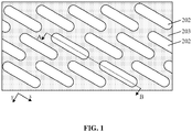
- FIG. 1-FIG. 12 are schematic structure diagrams of a memory forming process according to embodiments of the disclosure.
- a trench transistor of a memory still has the problems of high threshold voltage, low switching speed, and low working current.
- the threshold voltage, switching speed, and working current of the trench transistor of the memory are limited by the control capability of a word line and the width of a channel.
- the control capability of a word line is limited and the width of a channel is limited.
- a word line trench is formed in active regions and an isolation layer.
- the formed word line trench includes a first partial word line trench located in the active regions and a second partial word line trench located in the isolation layer.
- the first partial word line trench is interconnected with the second partial word line trench.
- a width and a depth of the second partial word line trench are greater than a width and a depth of the first partial word line trench respectively. Therefore, when a word line structure is formed in the word line trench, the formed word line structure accordingly includes a first partial word line structure located in the first partial word line trench and a second partial word line structure located in the second partial word line trench.
- the first partial word line structure is interconnected with the second partial word line structure.
- a width and a depth of the second partial word line structure are both greater than a width and a depth of the first partial word line structure.
- FIG. 1-FIG. 12 are schematic structure diagrams of a memory forming process according to embodiments of the disclosure.
- FIG. 2 is a schematic diagram showing a cross-sectional structure of FIG. 1 in a direction of a cutting line AB.
- a semiconductor substrate 201 is provided.
- a plurality of separate active regions 202 are formed on the semiconductor substrate 201.
- the plurality of active regions 202 are isolated through an isolation layer 203.
- the semiconductor substrate 201 may be made of silicon (Si), germanium (Ge), silicon germanium (GeSi), silicon carbide (SiC), silicon-on-insulator (SOI), germaniumon-insulator (GOI), or other materials, e.g. III-V group compounds such as gallium arsenide.
- the semiconductor substrate 201 is made of silicon in the present embodiment.
- Certain impurity ions are doped in the semiconductor substrate as required.
- the impurity ions may be N-type impurity ions or P-type impurity ions.
- the doping includes well region doping and source/drain region doping.
- a forming process of the active regions 202 and the isolation layer 203 is as follows.
- a first mask layer (not shown in the figure) is formed on the semiconductor substrate 201, where a plurality of first mask openings are arranged in parallel in the first mask layer.
- the semiconductor substrate 201 is etched along the first mask openings by taking the first mask layer as a mask, to form a plurality of separate strip-shaped active regions in the semiconductor substrate 201.
- a first trench is provided between every two adjacent strip-shaped active regions.
- the strip-shaped active regions are etched to form a plurality of second trenches in the strip-shaped active regions. Each of the strip-shaped active regions is divided into a plurality of active regions 202 by the second trenches.
- the isolation layer 203 may be made of silicon oxide or other suitable isolation materials.
- the first trench may be filled with an isolation material to form a first isolation layer
- the strip-shaped active regions are etched after the first isolation layer is formed, a plurality of second trenches are formed in the strip-shaped active regions, and then the second trench is filled with an isolation material to form a second isolation layer, where the first isolation layer and the second isolation layer form an isolation layer).
- the active regions 202 and the semiconductor substrate 201 are separated by a dashed line in order to conveniently identify the active regions 202 and the semiconductor substrate 201.
- the active regions 202 may be formed by an epitaxial process.
- an x-axis direction shown in FIG. 1 may be used as a row direction
- a y-axis direction shown in FIG. 1 may be used as a column direction
- the positions of the active regions 202 in adjacent rows may have a certain misalignment.
- FIG. 4 is a schematic diagram showing a cross-sectional structure of FIG. 3 in a direction of a cutting line AB.
- a mask layer 210 is formed on the active regions 202 and the isolation layer 203.
- the mask layer 210 is a hard mask layer.
- the mask layer 210 may be made of one or more of silicon oxide, silicon nitride, and silicon oxynitride.
- the mask layer 210 may be of a single-layer or multi-layer stacked structure.
- the mask layer 210 includes a silicon nitride layer, an amorphous carbon layer on the silicon nitride layer, an inorganic anti-reflective coating on the amorphous carbon layer, and a photoresist layer on the inorganic anti-reflective coating.
- the silicon nitride layer and the amorphous carbon layer are formed by a chemical vapor deposition process, and the inorganic anti-reflective coating and the photoresist layer are formed by a spin coating process.
- FIG. 6 is a schematic diagram showing a cross-sectional structure of FIG. 5 in a direction of a cutting line AB.
- a plurality of parallel openings 211 are formed in the mask layer 210.
- An extending direction of the openings 211 and an extending direction of the active regions 202 form an angle.
- Each of the openings 211 includes a plurality of first openings 211a and a plurality of second openings 211b which are arranged alternately.
- the first opening 211a is interconnected with the second opening 211b.
- the width of each of the second openings 211b is greater than the width of each of the first openings 211a.
- a partial surface of the active regions 202 is exposed from the bottom of the first opening 211a.
- a partial surface of the isolation layer 203 between two adjacent ones of the active regions 202 is exposed from the second opening 211b.
- the mask layer 210 is patterned to form the opening 211 in the mask layer 210. Specifically, the photoresist layer in the mask layer 210 is exposed and developed to pattern the photoresist. Then, the remaining mask layer 210 is etched by taking the patterned photoresist layer as a mask, to form the opening 211 in the mask layer 211.
- the remaining mask layer 210 is etched by using an anisotropic dry plasma etching process.
- the anisotropic dry plasma etching process includes a first dry plasma etching step, a second dry plasma etching step, a third dry plasma etching step, and a fourth dry plasma etching step.
- a photoresist base film is removed from the photoresist by using the first dry plasma etching step.
- a gas used in the first dry plasma etching step includes O 2 and Cl 2 .
- a flow range of O 2 is 5-15 sccm.
- a flow range of Cl 2 is 5-15 sccm.
- An etching time is 3-8 s.
- the inorganic anti-reflective coating is etched by using the second dry plasma etching step.
- a gas used in the second dry plasma etching step includes HBr and CF 4 .
- a flow range of HBr is 80-90 sccm.
- a flow range of CF 4 is 150-180 sccm.
- An etching time is 25-35 s.
- the amorphous carbon layer is etched by using the third dry plasma etching step.
- a gas used in the third dry plasma etching step includes O 2 and SO 2 .
- a flow range of O 2 is 80-90 sccm.
- a flow range of SO 2 is 150-180 sccm.
- An etching time is 70-90 s.
- the silicon nitride layer is etched by using the fourth dry plasma etching step.
- a gas used in the fourth dry plasma etching step includes CF 4 , CH 2 F 2 , and He.
- a flow range of CF 4 is 40-60 sccm.
- a flow range of CH 2 F 2 is 15-25 sccm.
- a flow range of He is 90-110 sccm.
- An etching time is 25-35 s.
- the mask layer 210 serves as a mask when the active regions 202 and the isolation layer 203 are subsequently etched to form the word line trench.
- the opening 211 formed in the mask layer 210 includes a plurality of first openings 211a and a plurality of second openings 211b which are arranged alternately.
- the first opening 211a is interconnected with the second opening 211b.
- the width of each of the second openings 211b is greater than the width of each of the first openings 211a.
- a partial surface of the active regions 202 is exposed from the bottom of the first opening 211a.
- a partial surface of the isolation layer 203 between two adjacent ones of the active regions 202 is exposed from the second opening 211b.
- the active regions 202 and the isolation layer 203 are etched along the first openings 211a and the second openings 211b by taking the mask layer 210 as a mask.
- the corresponding word line trench includes a first partial word line trench located in the active regions (corresponding to the width and position of the first opening 211a) and a second partial word line trench located in the isolation layer (corresponding to the width and position of the second opening 211b).
- the first partial word line trench is interconnected with the second partial word line trench, and the width and depth of the second partial word line trench are greater than the corresponding width and depth of the first partial word line trench respectively.
- the foregoing word line trench with a specific shape may be formed simply and conveniently by only one patterning process of the mask layer and one etching process of the active regions 202 and the isolation layer 203. Moreover, the positional and dimensional accuracy of the first partial word line trench and the second partial word line trench in the formed word line trench is high, and the performance of the subsequently formed word line structure is improved.
- FIG. 8 is a schematic diagram showing a cross-sectional structure of FIG. 7 in a direction of a cutting line AB.
- the active regions 202 and the isolation layer 203 are partially etched away by taking the mask layer 210 as a mask.
- a word line trench 204 is formed in the active regions 202 and the isolation layer 203.
- the word line trench 204 includes a first partial word line trench 204a located in the active regions 202 and a second partial word line trench 204b located in the isolation layer 203.
- the first partial word line trench 204a is interconnected with the second partial word line trench 204b.
- the width W1 and depth of the second partial word line trench 204b are greater than the corresponding width W2 and depth of the first partial word line trench 204a respectively.
- the formed word line trench 204 includes a first partial word line trench 204a located in the active regions 202 and a second partial word line trench 204b located in the isolation layer 203.
- the first partial word line trench 204a is interconnected with the second partial word line trench 204b.
- the width W1 and depth of the second partial word line trench 204b are both greater than the width W2 and depth of the first partial word line trench 204a. Therefore, when a word line structure is formed in the word line trench 204 subsequently, the formed word line structure also includes a first partial word line structure located in the first partial word line trench and a second partial word line structure located in the second partial word line trench.
- the first partial word line structure is interconnected with the second partial word line structure.
- the width and depth of the second partial word line structure are both greater than the corresponding width and depth of the first partial word line structure.
- a "fin-type" word line structure across the active regions increases the contact area between the word line structure and the active regions, so that the control capability of the word line structure on a channel is improved, and the working frequency of a trench transistor is improved. Therefore, the working frequency of a memory (DRAM) is improved.
- the width of the channel of the trench transistor is increased, the working current of the trench transistor is increased, the threshold voltage of the trench transistor is reduced, and the performance of the memory (DRAM) is improved.
- the active regions 202 and the isolation layer 203 are etched along the opening in the mask layer 210. Lateral etching the isolation layer 203 is added during the etching. Then, the word line trench 204 is formed in the active regions 202 and the isolation layer 203.
- the etching process includes: adding an isotropic dry plasma etching step in an anisotropic dry plasma etching step. The isotropic dry plasma etching step is used for laterally etching the isolation layer 203 (when the isotropic dry plasma etching step is performed, the etching rate of the isolation layer 203 is far greater than the etching rate of the active regions 202, i.e.
- an etching gas used in the anisotropic dry plasma etching step includes one or more selected from Cl 2 , HBr, CF 4 , CHF 3 .
- An etching gas used in the isotropic dry plasma etching step includes one or more selected from CF 4 , CHF 3 , CH 2 F 2 .
- the etching gas used in the anisotropic dry plasma etching step further includes one or more selected from helium or argon.
- the foregoing etching process for forming the word line trench 204 includes the following operations. Firstly, anisotropic dry plasma etching is performed to etch the active regions 202 and the isolation layer 203 by taking the mask layer 210 as a mask, such that a first etching trench in the active regions 202 and the isolation layer 203 is formed. The etching time is 15-25 s.
- the used etching gas includes Cl 2 , HBr, CF 4 , CHF 3 , and He.
- the flow range of Cl 2 is 15-20 sccm
- the flow range of HBr is 30-40 sccm
- the flow range of CF 4 is 110-130 sccm
- the flow range of CHF 3 is 90-110 sccm
- the flow range of He is 90-110 sccm.
- isotropic dry plasma etching is performed to etch the isolation layer 203 at two sides of the first etching trench (in the same etching chamber), so that the width and depth of the corresponding part of the first etching trench in the isolation layer 203 are increased.
- the etching time is 3-8 s.
- the used etching gas includes CF 4 and CH 2 F 2 .
- the flow range of CF 4 is 40-60 ccm, and the flow range of CH 2 F 2 is 18-33 sccm.
- the anisotropic dry plasma etching is performed again, so that the depth of the first etching trench is increased until the word line trench 204 is formed in the active regions 202 and the isolation layer 203.
- the etching time is 15-25 s.
- the used etching gas includes Cl 2 , HBr, CF 4 , CHF 3 , and He.
- the flow range of Cl 2 is 15-20 sccm
- the flow range of HBr is 30-40 sccm
- the flow range of CF 4 is 110-130 sccm
- the flow range of CHF 3 is 90-110 sccm
- the flow range of He is 90-110 sccm.
- the word line trench 204 is formed by combining the foregoing etching steps and the foregoing specific etching process parameters, so that the width and depth precision of the second partial word line trench 204b formed in the isolation layer 203 are further improved, the occurrence of electricity leakage can be better prevented, and smaller width and depth dimensions of the second partial word line trench 204b can be better controlled.
- the width W2 of the first partial word line trench 204a is 17-25 nm, and the width W1 of the second partial word line trench 204b is 20-30 nm.
- the second partial word line trench 204b is wider than the first partial word line trench 204a by a width range (W1-W2) of 6-9 nm.
- the second partial word line trench 204b is deeper than the first partial word line trench 204a by a depth range D1 of 3-5 nm.
- each active region 202 there are two word line trenches 204 in each active region 202 to facilitate the subsequent formation of a dual-trench transistor.
- the two word line trenches 204 divide each active region 202 into a drain located in the middle and two sources located at two sides of the drain respectively.
- the forming process of the word line trench includes the following operations.
- a mask layer is formed on the active regions and the isolation layer, where the mask layer has a plurality of parallel openings (the widths of different positions of the openings are uniform or substantially the same), an extending direction of the openings and an extending direction of the active regions form an angle, and both a partial surface of the active regions and a partial surface of the isolation layer are exposed from each of the openings.
- the active regions and the isolation layer are etched along the openings, and lateral etching the isolation layer is added during the etching process, such that the word line trench in the active regions and the isolation layer is formed.
- the formed word line trench includes a first partial word line trench located in the active regions and a second partial word line trench located in the isolation layer.
- the first partial word line trench is interconnected with the second partial word line trench.
- the width and depth of the second partial word line trench are greater than the corresponding width and depth of the first partial word line trench respectively.
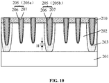
- FIG. 10 is a schematic diagram showing a cross-sectional structure of FIG. 9 in a direction of a cutting line AB.
- a word line structure 205 is formed in the word line trench 204 (referring to FIG. 7 ).
- the word line structure 205 includes a first partial word line structure 205a located in the first partial word line trench and a second partial word line structure 205b located in the second partial word line trench.
- the first partial word line structure 205a is interconnected with the second partial word line structure 205b.
- the width D1 and depth of the second partial word line structure 205b are greater than the width D2 and depth of the first partial word line structure 205a respectively.
- the word line structure 205 includes a gate dielectric layer 206 located both on the side walls and bottom surface of the word line trench, and a metal electrode 207 located on the gate dielectric layer 206 for filling the word line trench.
- the gate dielectric layer 205 may include a silicon oxide layer located on the sidewalls and bottom surface of the word line trench, and a barrier layer located on the silicon oxide layer.
- the metal electrode 207 may be made of tungsten (W) or other suitable metal materials, and the barrier layer may be made of TiN.
- the width of the first partial word line structure 205a is 17-25 nm.
- the width of the second partial word line structure 205b is 20-30 nm.
- the second partial word line structure 205b is wider than the first partial word line structure 205a by a width range of 6-9 nm.
- the second partial word line structure 205b is deeper than the first partial word line structure 205a by a depth range of 3-5 nm. In this way, the control capability of the word line structure on the channel is higher, and accordingly the working frequency of the memory (DRAM) can be higher, while the integration level of the memory (DRAM) is ensured.
- the forming process of the word line structure 205 includes the following operations.
- a silicon oxide layer is formed both on the side walls and bottom surface of the word line trench, in particular by a thermal oxidation process.
- a barrier layer is formed on the silicon oxide layer and the mask layer 210.
- a metal layer is formed on the barrier layer. The metal layer and the barrier layer, higher than the surface of the mask layer 210, are removed by flattening, to form the word line structure 205.
- FIG. 11 is performed on the basis of FIG. 10 .
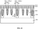
- the word line structure of a certain thickness is removed by etching back, so that the top surface of the remaining word line structure 205 is lower than the surface of the active regions 202 (referring to FIG. 11 ).
- the top of the remaining metal layer may be " ⁇ -shaped" (not shown in the figure).
- a protective layer 212 is formed to cover the remaining word line structure 205 and the mask layer 210.
- the top surface of the remaining word line structure 205 is lower than the top surface of the active regions 202 by a depth range D2 of 60-75 nm.
- the protective layer 212 may be used to prevent oxidation of the metal electrode 207 in the word line structure 205.
- the protective layer 212 is made of silicon nitride or other suitable materials.
- the method may further include: forming a bit line (not shown in the figure) connected with the drain region and a capacitor (not shown in the figure) connected with the two source regions respectively.
- the memory includes a semiconductor substrate 201, a word line trench, and a word line structure 205.
- the semiconductor substrate 201 has a plurality of separate active regions 202.
- the plurality of active regions 202 are isolated through an isolation layer 203.
- the word line trench is located in the active regions 202 and the isolation layer 203.
- the word line trench includes a first partial word line trench located in the active regions and a second partial word line trench located in the isolation layer.
- the first partial word line trench is interconnected with the second partial word line trench.
- the width and depth of the second partial word line trench are greater than the corresponding width and depth of the first partial word line trench respectively.
- the word line structure 205 is located in the word line trench.
- the word line structure 205 includes a first partial word line structure 205a located in the first partial word line trench and a second partial word line structure 205b located in the second partial word line trench.
- the first partial word line structure 205a is interconnected with the second partial word line structure 205b.
- the width D1 and depth of the second partial word line structure 205b are greater than the corresponding width D2 and depth of the first partial word line structure 205a respectively.
- the width of the first partial word line structure 205a is 17-25 nm.
- the width of the second partial word line structure 205b is 20-30 nm.
- the second partial word line structure 205b is wider than the first partial word line structure 205a by a width range of 6-9 nm.
- the second partial word line structure 205b is deeper than the first partial word line structure 205a by a depth range of 3-5 nm.
- a top surface of the word line structure 205 is lower than a surface of the active regions 202.
- the word line structure 205 includes a gate dielectric layer 206 located both on the side walls and bottom of the word line trench, and a metal electrode 207 located on the gate dielectric layer 206 for filling the word line trench.
- the top surface of the word line structure 205 is lower than the top surface of the active regions 202 by a depth range of 60-75 nm.
- Two separate word line trenches are formed in each active region 202.
- the two word line trenches divide each active region into a drain region located in the middle and two source regions located at two sides of the drain region.
- the two separate word line trenches have respective word line structures therein.
- a bit line connected with the drain region and a capacitor connected with the two source regions respectively are further included.
- DRAM memory
- DRAM dynamic random access memory
Landscapes
- Engineering & Computer Science (AREA)
- Manufacturing & Machinery (AREA)
- Semiconductor Memories (AREA)
Abstract
Description
- The present application claims priority to
Chinese patent application No. 202010242398.5, filed on March 31, 2020 - The disclosure relates to the field of memories, and in particular to a memory and a method for forming the same.
- A Dynamic Random Access Memory (DRAM) is a semiconductor memory device commonly used in computers, which is composed of a plurality of repeated memory units. Each of the memory units usually includes a capacitor and a transistor. A gate of the transistor is interconnected with a word line, a drain of the transistor is interconnected with a bit line, and a source of the transistor is interconnected with the capacitor. Voltage signals on the word line may control turn-on or turn-off of the transistor, so that data information stored in the capacitor may be read through the bit line, or data information may be written into the capacitor through the bit line for storage.
- In order to improve the integration level of a memory structure, the transistor in the DRAM usually uses a trench transistor structure. A specific structure of the trench transistor structure includes a semiconductor substrate, a trench located in the semiconductor substrate, a gate (or a word line structure) located in the trench, and a source region and a drain region located at two sides of the trench in the semiconductor substrate. The gate of the trench transistor is interconnected with the word line, the drain region is interconnected with the bit line, and the source region is interconnected with the capacitor.
- The trench transistor of the conventional DRAM still has the problems of high threshold voltage, low switching speed, and low working current.
- The technical problem to be solved by the disclosure is how to reduce a high threshold voltage of a trench transistor of a DRAM and improve a switching speed and a working current.
- To this end, the disclosure provides a method for forming a memory, which may include:
- providing a semiconductor substrate, where a plurality of separate active regions may be formed on the semiconductor substrate and isolated through an isolation layer;
- forming a word line trench both in the active regions and the isolation layer by etching, where the word line trench may include a first partial word line trench located in the active regions and a second partial word line trench located in the isolation layer, the first partial word line trench may be interconnected with the second partial word line trench, and a width and a depth of the second partial word line trench may be greater than a width and a depth of the first partial word line trench respectively; and
- forming a word line structure in the word line trench, where the word line structure may include a first partial word line structure located in the first partial word line trench and a second partial word line structure located in the second partial word line trench, the first partial word line structure may be interconnected with the second partial word line structure, and a width and a depth of the second partial word line structure may be greater than a width and a depth of the first partial word line structure respectively.
- Optionally, a forming process of the word line trench may include: forming a mask layer on the active regions and the isolation layer, where the mask layer may have a plurality of parallel openings, an extending direction of the openings and an extending direction of the active regions may form an angle, and both a partial surface of the active regions and a partial surface of the isolation layer may be exposed from each of the openings; and etching the active regions and the isolation layer along the openings, where lateral etching the isolation layer is added during the etching, to form the word line trench both in the active regions and the isolation layer.
- Optionally, the etching may include: adding an isotropic dry plasma etching step in an anisotropic dry plasma etching step, where the isotropic dry plasma etching step may be used for laterally etching the isolation layer.
- Optionally, an etching gas used in the anisotropic dry plasma etching step may include one or more selected from Cl2, HBr, CF4, or CHF3, and an etching gas used in the isotropic dry plasma etching step may include one or more selected from CF4, CHF3, or CH2F2.
- Optionally, the etching gas used in the anisotropic dry plasma etching step may further include one or more selected from helium or argon.
- Optionally, a forming process of the word line trench may include: forming a mask layer on the active regions and the isolation layer, where the mask layer may have a plurality of parallel openings, an extending direction of the openings and an extending direction of the active regions may form an angle, each of the openings may include a plurality of first openings and a plurality of second openings which are arranged alternately and interconnected with each other, a width of each of the second openings may be greater than a width of each of the first openings, a partial surface of the active regions may be exposed from a bottom of the first opening, and a partial surface of the isolation layer between two adjacent ones of the active regions may be exposed from the second opening; etching the active regions and the isolation layer along the first openings and the second openings, to form the word line trench both in the active regions and the isolation layer.
- Optionally, the etching the active regions and the isolation layer along the first openings and the second openings may be performed by using an anisotropic dry plasma etching process.
- Optionally, the width of the first partial word line trench is 17-25 nm and the width of the second partial word line trench is 20-30 nm.
- Optionally, the second partial word line trench is wider than the first partial word line trench by a width range of 6-9 nm, and the second partial word line trench is deeper than the first partial word line trench by a depth range of 3-5 nm.
- Optionally, the active regions may be made of silicon and the isolation layer may be made of silicon oxide.
- Optionally, the word line structure may include a gate dielectric layer located both on side walls and a bottom of the word line trench, and a metal electrode located on the gate dielectric layer for filling the word line trench.
- Optionally, a forming process of the word line structure may include: forming a silicon oxide layer both on the side walls and a bottom surface of the word line trench; forming a barrier layer on the silicon oxide layer; forming a metal layer on the barrier layer; partially removing the metal layer and the barrier layer by flattening to form the word line structure; and removing the word line structure of a certain thickness by etching back, so that a top surface of the remaining word line structure is lower than a surface of the active regions.
- Optionally, the top surface of the remaining word line structure is lower than the top surface of the active regions by a depth range of 60-75 nm.
- Optionally, a protective layer may be formed to cover the remaining word line structure.
- The disclosure also provides a memory, which may include:
- a semiconductor substrate, where the semiconductor substrate may have a plurality of separate active regions, which may be isolated through an isolation layer;
- a word line trench located in the active regions and the isolation layer, where the word line trench may include a first partial word line trench located in the active regions and a second partial word line trench located in the isolation layer, the first partial word line trench may be interconnected with the second partial word line trench, and a width and a depth of the second partial word line trench may be greater than a width and a depth of the first partial word line trench respectively; and
- a word line structure located in the word line trench, where the word line structure may include a first partial word line structure located in the first partial word line trench and a second partial word line structure located in the second partial word line trench, the first partial word line structure may be interconnected with the second partial word line structure, and a width and a depth of the second partial word line structure may be greater than a width and a depth of the first partial word line structure respectively.
- Optionally, the width of the first partial word line structure may be 17-25 nm and the width of the second partial word line structure may be 20-30 nm.
- Optionally, the second partial word line structure is wider than the first partial word line structure by a width range of 6-9 nm, and the second partial word line structure is deeper than the first partial word line structure by a depth range of 3-5 nm.
- Optionally, the top surface of the word line structure may be lower than the surface of the active region, and the word line structure may include a gate dielectric layer located both on side walls and a bottom of the word line trench, and a metal electrode located on the gate dielectric layer for filling the word line trench.
- Optionally, the top surface of the remaining word line structure may be lower than the top surface of the active regions by a depth range of 60-75 nm.
- Compared with the prior art, the technical solution of the disclosure has the following advantages.
- According to the method for forming a memory of the disclosure, a word line trench is formed in active regions and an isolation layer. The formed word line trench includes a first partial word line trench located in the active regions and a second partial word line trench located in the isolation layer. The first partial word line trench is interconnected with the second partial word line trench. The width and depth of the second partial word line trench are greater than the corresponding width and depth of the first partial word line trench respectively. Therefore, when a word line structure is formed in the word line trench, the formed word line structure also includes a first partial word line structure located in the first partial word line trench and a second partial word line structure located in the second partial word line trench. The first partial word line structure is interconnected with the second partial word line structure. The width and depth of the second partial word line structure are both greater than the corresponding width and depth of the first partial word line structure. Indeed, such a "fin-type" word line structure across the active regions increases the contact area between the word line structure and the active regions, so that the control capability of the word line structure on a channel is improved, and the working frequency of a trench transistor is improved. Therefore, the working frequency of a memory (DRAM) is improved. Furthermore, by means of such a structure, the width of the channel of the trench transistor is increased, the working current of the trench transistor is increased, the threshold voltage of the trench transistor is reduced, and the performance of the memory (DRAM) is improved.
- Further, the forming process of the word line trench includes: forming a mask layer on the active regions and the isolation layer, where the mask layer has a plurality of parallel openings, an extending direction of the openings and an extending direction of the active regions form an angle, each of the openings includes a plurality of first openings and a plurality of second openings which are arranged alternately and interconnected with each other, the width of each of the second openings is greater than the width of each of the first openings, a partial surface of the active regions is exposed from the bottom of the first opening, and a partial surface of the isolation layer between two adjacent ones of the active regions is exposed from the second opening; etching the active regions and the isolation layer along the first openings and the second openings, and forming the word line trench both in the active regions and the isolation layer, where the formed word line trench includes a first partial word line trench located in the active regions and a second partial word line trench located in the isolation layer, the first partial word line trench is interconnected with the second partial word line trench, and the width and depth of the second partial word line trench are greater than the corresponding width and depth of the first partial word line trench respectively. According to the foregoing method, the foregoing word line trench with a specific shape may be formed simply and conveniently by only one patterning process of the mask layer and one etching process of the active regions and the isolation layer. Moreover, the positional and dimensional accuracy of the first partial word line trench and the second partial word line trench in the formed word line trench is high, and the performance of the subsequently formed word line structure is improved.
- According to the memory of the disclosure, a word line trench is provided in active regions and an isolation layer. The word line trench includes a first partial word line trench located in the active regions and a second partial word line trench located in the isolation layer. The first partial word line trench is interconnected with the second partial word line trench. The width and depth of the second partial word line trench are greater than the corresponding width and depth of the first partial word line trench respectively. Correspondingly, when a word line structure is provided in the word line trench, the word line structure also includes a first partial word line structure located in the first partial word line trench and a second partial word line structure located in the second partial word line trench. The first partial word line structure is interconnected with the second partial word line structure. The width and depth of the second partial word line structure are both greater than the corresponding width and depth of the first partial word line structure. Indeed, such a "fin-type" word line structure across the active regions increases the contact area between the word line structure and the active regions, so that the control capability of the word line structure on a channel is improved, and the working frequency of a trench transistor is improved. Therefore, the working frequency of a memory (DRAM) is improved. Furthermore, by means of such a structure, the width of the channel of the trench transistor is increased, the working current of the trench transistor is increased, the threshold voltage of the trench transistor is reduced, and the performance of the memory (DRAM) is improved.
-
FIG. 1-FIG. 12 are schematic structure diagrams of a memory forming process according to embodiments of the disclosure. - As described in BACKGROUND, a trench transistor of a memory (DRAM) still has the problems of high threshold voltage, low switching speed, and low working current.
- It has been found that the threshold voltage, switching speed, and working current of the trench transistor of the memory (DRAM) are limited by the control capability of a word line and the width of a channel. In a conventional memory (DRAM), the control capability of a word line is limited and the width of a channel is limited.
- To this end, the disclosure provides a memory and a method for forming the memory. According to the method, a word line trench is formed in active regions and an isolation layer. The formed word line trench includes a first partial word line trench located in the active regions and a second partial word line trench located in the isolation layer. The first partial word line trench is interconnected with the second partial word line trench. A width and a depth of the second partial word line trench are greater than a width and a depth of the first partial word line trench respectively. Therefore, when a word line structure is formed in the word line trench, the formed word line structure accordingly includes a first partial word line structure located in the first partial word line trench and a second partial word line structure located in the second partial word line trench. The first partial word line structure is interconnected with the second partial word line structure. A width and a depth of the second partial word line structure are both greater than a width and a depth of the first partial word line structure. Indeed, such a "fin-type" word line structure across the active regions increases the contact area between the word line structure and the active regions, so that the control capability of the word line structure on a channel is improved, and the working frequency of a trench transistor is improved. Therefore, the working frequency of a memory (DRAM) is improved. Furthermore, by means of such a structure, the width of the channel of the trench transistor is increased, the working current of the trench transistor is increased, the threshold voltage of the trench transistor is reduced, and the performance of the memory (DRAM) is improved.
- In order that the above objects, features, and advantages of the disclosure can be more readily understood, specific implementations of the disclosure will now be described in detail with reference to the accompanying drawings. In the detailed description of the embodiments of the disclosure, for convenience of description, the schematic diagram will be partially enlarged but not to scale, and the schematic diagram is only illustrative, which should not be construed as limitations to the protection scope of the disclosure. In addition, three-dimensional space dimensions of length, width, and depth should be included in actual production.
-
FIG. 1-FIG. 12 are schematic structure diagrams of a memory forming process according to embodiments of the disclosure. - Referring to
FIG. 1-FIG. 2 ,FIG. 2 is a schematic diagram showing a cross-sectional structure ofFIG. 1 in a direction of a cutting line AB. Asemiconductor substrate 201 is provided. A plurality of separateactive regions 202 are formed on thesemiconductor substrate 201. The plurality ofactive regions 202 are isolated through anisolation layer 203. - The
semiconductor substrate 201 may be made of silicon (Si), germanium (Ge), silicon germanium (GeSi), silicon carbide (SiC), silicon-on-insulator (SOI), germaniumon-insulator (GOI), or other materials, e.g. III-V group compounds such as gallium arsenide. Thesemiconductor substrate 201 is made of silicon in the present embodiment. Certain impurity ions are doped in the semiconductor substrate as required. The impurity ions may be N-type impurity ions or P-type impurity ions. In one embodiment, the doping includes well region doping and source/drain region doping. - A forming process of the
active regions 202 and theisolation layer 203 is as follows. A first mask layer (not shown in the figure) is formed on thesemiconductor substrate 201, where a plurality of first mask openings are arranged in parallel in the first mask layer. Thesemiconductor substrate 201 is etched along the first mask openings by taking the first mask layer as a mask, to form a plurality of separate strip-shaped active regions in thesemiconductor substrate 201. A first trench is provided between every two adjacent strip-shaped active regions. The strip-shaped active regions are etched to form a plurality of second trenches in the strip-shaped active regions. Each of the strip-shaped active regions is divided into a plurality ofactive regions 202 by the second trenches. An isolation material is filled in the first trench and the second trench to form anisolation layer 203. Theisolation layer 203 may be made of silicon oxide or other suitable isolation materials. (In other embodiments, the first trench may be filled with an isolation material to form a first isolation layer, the strip-shaped active regions are etched after the first isolation layer is formed, a plurality of second trenches are formed in the strip-shaped active regions, and then the second trench is filled with an isolation material to form a second isolation layer, where the first isolation layer and the second isolation layer form an isolation layer). It is to be noted that theactive regions 202 and thesemiconductor substrate 201 are separated by a dashed line in order to conveniently identify theactive regions 202 and thesemiconductor substrate 201. - In other embodiments, the
active regions 202 may be formed by an epitaxial process. - In the present embodiment, an x-axis direction shown in
FIG. 1 may be used as a row direction, a y-axis direction shown inFIG. 1 may be used as a column direction, and the positions of theactive regions 202 in adjacent rows may have a certain misalignment. - Referring to
FIG. 3 andFIG. 4, FIG. 4 is a schematic diagram showing a cross-sectional structure ofFIG. 3 in a direction of a cutting line AB. Amask layer 210 is formed on theactive regions 202 and theisolation layer 203. - The
mask layer 210 is a hard mask layer. Themask layer 210 may be made of one or more of silicon oxide, silicon nitride, and silicon oxynitride. Themask layer 210 may be of a single-layer or multi-layer stacked structure. - In the present embodiment, the
mask layer 210 includes a silicon nitride layer, an amorphous carbon layer on the silicon nitride layer, an inorganic anti-reflective coating on the amorphous carbon layer, and a photoresist layer on the inorganic anti-reflective coating. The silicon nitride layer and the amorphous carbon layer are formed by a chemical vapor deposition process, and the inorganic anti-reflective coating and the photoresist layer are formed by a spin coating process. - Referring to
FIG. 5 andFIG. 6, FIG. 6 is a schematic diagram showing a cross-sectional structure ofFIG. 5 in a direction of a cutting line AB. A plurality ofparallel openings 211 are formed in themask layer 210. An extending direction of theopenings 211 and an extending direction of theactive regions 202 form an angle. Each of theopenings 211 includes a plurality offirst openings 211a and a plurality ofsecond openings 211b which are arranged alternately. Thefirst opening 211a is interconnected with thesecond opening 211b. The width of each of thesecond openings 211b is greater than the width of each of thefirst openings 211a. A partial surface of theactive regions 202 is exposed from the bottom of thefirst opening 211a. A partial surface of theisolation layer 203 between two adjacent ones of theactive regions 202 is exposed from thesecond opening 211b. - The
mask layer 210 is patterned to form theopening 211 in themask layer 210. Specifically, the photoresist layer in themask layer 210 is exposed and developed to pattern the photoresist. Then, the remainingmask layer 210 is etched by taking the patterned photoresist layer as a mask, to form theopening 211 in themask layer 211. - In the present embodiment, the remaining
mask layer 210 is etched by using an anisotropic dry plasma etching process. The anisotropic dry plasma etching process includes a first dry plasma etching step, a second dry plasma etching step, a third dry plasma etching step, and a fourth dry plasma etching step. Specifically, a photoresist base film is removed from the photoresist by using the first dry plasma etching step. A gas used in the first dry plasma etching step includes O2 and Cl2. A flow range of O2 is 5-15 sccm. A flow range of Cl2 is 5-15 sccm. An etching time is 3-8 s. The inorganic anti-reflective coating is etched by using the second dry plasma etching step. A gas used in the second dry plasma etching step includes HBr and CF4. A flow range of HBr is 80-90 sccm. A flow range of CF4 is 150-180 sccm. An etching time is 25-35 s. The amorphous carbon layer is etched by using the third dry plasma etching step. A gas used in the third dry plasma etching step includes O2 and SO2. A flow range of O2 is 80-90 sccm. A flow range of SO2 is 150-180 sccm. An etching time is 70-90 s. The silicon nitride layer is etched by using the fourth dry plasma etching step. A gas used in the fourth dry plasma etching step includes CF4, CH2F2, and He. A flow range of CF4 is 40-60 sccm. A flow range of CH2F2 is 15-25 sccm. A flow range of He is 90-110 sccm. An etching time is 25-35 s. - The
mask layer 210 serves as a mask when theactive regions 202 and theisolation layer 203 are subsequently etched to form the word line trench. In the present embodiment, theopening 211 formed in themask layer 210 includes a plurality offirst openings 211a and a plurality ofsecond openings 211b which are arranged alternately. Thefirst opening 211a is interconnected with thesecond opening 211b. The width of each of thesecond openings 211b is greater than the width of each of thefirst openings 211a. A partial surface of theactive regions 202 is exposed from the bottom of thefirst opening 211a. A partial surface of theisolation layer 203 between two adjacent ones of theactive regions 202 is exposed from thesecond opening 211b. Subsequently, theactive regions 202 and theisolation layer 203 are etched along thefirst openings 211a and thesecond openings 211b by taking themask layer 210 as a mask. When a word line trench is formed in theactive regions 202 and theisolation layer 203, the corresponding word line trench includes a first partial word line trench located in the active regions (corresponding to the width and position of thefirst opening 211a) and a second partial word line trench located in the isolation layer (corresponding to the width and position of thesecond opening 211b). The first partial word line trench is interconnected with the second partial word line trench, and the width and depth of the second partial word line trench are greater than the corresponding width and depth of the first partial word line trench respectively. Therefore, according to the foregoing method, the foregoing word line trench with a specific shape may be formed simply and conveniently by only one patterning process of the mask layer and one etching process of theactive regions 202 and theisolation layer 203. Moreover, the positional and dimensional accuracy of the first partial word line trench and the second partial word line trench in the formed word line trench is high, and the performance of the subsequently formed word line structure is improved. - Referring to
FIG. 7 andFIG. 8, FIG. 8 is a schematic diagram showing a cross-sectional structure ofFIG. 7 in a direction of a cutting line AB. Theactive regions 202 and theisolation layer 203 are partially etched away by taking themask layer 210 as a mask. Aword line trench 204 is formed in theactive regions 202 and theisolation layer 203. Theword line trench 204 includes a first partialword line trench 204a located in theactive regions 202 and a second partialword line trench 204b located in theisolation layer 203. The first partialword line trench 204a is interconnected with the second partialword line trench 204b. The width W1 and depth of the second partialword line trench 204b are greater than the corresponding width W2 and depth of the first partialword line trench 204a respectively. - The formed
word line trench 204 includes a first partialword line trench 204a located in theactive regions 202 and a second partialword line trench 204b located in theisolation layer 203. The first partialword line trench 204a is interconnected with the second partialword line trench 204b. The width W1 and depth of the second partialword line trench 204b are both greater than the width W2 and depth of the first partialword line trench 204a. Therefore, when a word line structure is formed in theword line trench 204 subsequently, the formed word line structure also includes a first partial word line structure located in the first partial word line trench and a second partial word line structure located in the second partial word line trench. The first partial word line structure is interconnected with the second partial word line structure. The width and depth of the second partial word line structure are both greater than the corresponding width and depth of the first partial word line structure. Indeed, such a "fin-type" word line structure across the active regions increases the contact area between the word line structure and the active regions, so that the control capability of the word line structure on a channel is improved, and the working frequency of a trench transistor is improved. Therefore, the working frequency of a memory (DRAM) is improved. Furthermore, by means of such a structure, the width of the channel of the trench transistor is increased, the working current of the trench transistor is increased, the threshold voltage of the trench transistor is reduced, and the performance of the memory (DRAM) is improved. - In the present embodiment, the
active regions 202 and theisolation layer 203 are etched along the opening in themask layer 210. Lateral etching theisolation layer 203 is added during the etching. Then, theword line trench 204 is formed in theactive regions 202 and theisolation layer 203. In one embodiment, the etching process includes: adding an isotropic dry plasma etching step in an anisotropic dry plasma etching step. The isotropic dry plasma etching step is used for laterally etching the isolation layer 203 (when the isotropic dry plasma etching step is performed, the etching rate of theisolation layer 203 is far greater than the etching rate of theactive regions 202, i.e. the etching amount of theactive regions 202 is little or negligible). By the foregoing process, the width and depth of the second partialword line trench 204b formed in theisolation layer 203 can be accurately controlled to prevent the occurrence of electricity leakage, and the control of smaller width and depth dimensions of the second partialword line trench 204b can be realized. In one embodiment, an etching gas used in the anisotropic dry plasma etching step includes one or more selected from Cl2, HBr, CF4, CHF3. An etching gas used in the isotropic dry plasma etching step includes one or more selected from CF4, CHF3, CH2F2. In one embodiment, the etching gas used in the anisotropic dry plasma etching step further includes one or more selected from helium or argon. - In a specific embodiment, the foregoing etching process for forming the
word line trench 204 includes the following operations. Firstly, anisotropic dry plasma etching is performed to etch theactive regions 202 and theisolation layer 203 by taking themask layer 210 as a mask, such that a first etching trench in theactive regions 202 and theisolation layer 203 is formed. The etching time is 15-25 s. The used etching gas includes Cl2, HBr, CF4, CHF3, and He. The flow range of Cl2 is 15-20 sccm, the flow range of HBr is 30-40 sccm, the flow range of CF4 is 110-130 sccm, the flow range of CHF3 is 90-110 sccm, and the flow range of He is 90-110 sccm. Then, isotropic dry plasma etching is performed to etch theisolation layer 203 at two sides of the first etching trench (in the same etching chamber), so that the width and depth of the corresponding part of the first etching trench in theisolation layer 203 are increased. The etching time is 3-8 s. The used etching gas includes CF4 and CH2F2. The flow range of CF4 is 40-60 ccm, and the flow range of CH2F2 is 18-33 sccm. Next, the anisotropic dry plasma etching is performed again, so that the depth of the first etching trench is increased until theword line trench 204 is formed in theactive regions 202 and theisolation layer 203. The etching time is 15-25 s. The used etching gas includes Cl2, HBr, CF4, CHF3, and He. The flow range of Cl2 is 15-20 sccm, the flow range of HBr is 30-40 sccm, the flow range of CF4 is 110-130 sccm, the flow range of CHF3 is 90-110 sccm, and the flow range of He is 90-110 sccm. In the present embodiment, theword line trench 204 is formed by combining the foregoing etching steps and the foregoing specific etching process parameters, so that the width and depth precision of the second partialword line trench 204b formed in theisolation layer 203 are further improved, the occurrence of electricity leakage can be better prevented, and smaller width and depth dimensions of the second partialword line trench 204b can be better controlled. - In a specific embodiment, the width W2 of the first partial
word line trench 204a is 17-25 nm, and the width W1 of the second partialword line trench 204b is 20-30 nm. The second partialword line trench 204b is wider than the first partialword line trench 204a by a width range (W1-W2) of 6-9 nm. The second partialword line trench 204b is deeper than the first partialword line trench 204a by a depth range D1 of 3-5 nm. - In the present embodiment, there are two
word line trenches 204 in eachactive region 202 to facilitate the subsequent formation of a dual-trench transistor. Specifically, the twoword line trenches 204 divide eachactive region 202 into a drain located in the middle and two sources located at two sides of the drain respectively. - In other embodiments, the forming process of the word line trench includes the following operations. A mask layer is formed on the active regions and the isolation layer, where the mask layer has a plurality of parallel openings (the widths of different positions of the openings are uniform or substantially the same), an extending direction of the openings and an extending direction of the active regions form an angle, and both a partial surface of the active regions and a partial surface of the isolation layer are exposed from each of the openings. The active regions and the isolation layer are etched along the openings, and lateral etching the isolation layer is added during the etching process, such that the word line trench in the active regions and the isolation layer is formed. The formed word line trench includes a first partial word line trench located in the active regions and a second partial word line trench located in the isolation layer. The first partial word line trench is interconnected with the second partial word line trench. Moreover, the width and depth of the second partial word line trench are greater than the corresponding width and depth of the first partial word line trench respectively.
- Referring to
FIG. 9 andFIG. 10, FIG. 10 is a schematic diagram showing a cross-sectional structure ofFIG. 9 in a direction of a cutting line AB. Aword line structure 205 is formed in the word line trench 204 (referring toFIG. 7 ). Theword line structure 205 includes a first partialword line structure 205a located in the first partial word line trench and a second partialword line structure 205b located in the second partial word line trench. The first partialword line structure 205a is interconnected with the second partialword line structure 205b. The width D1 and depth of the second partialword line structure 205b are greater than the width D2 and depth of the first partialword line structure 205a respectively. - In one embodiment, the
word line structure 205 includes agate dielectric layer 206 located both on the side walls and bottom surface of the word line trench, and ametal electrode 207 located on thegate dielectric layer 206 for filling the word line trench. - In a specific embodiment, the
gate dielectric layer 205 may include a silicon oxide layer located on the sidewalls and bottom surface of the word line trench, and a barrier layer located on the silicon oxide layer. - The
metal electrode 207 may be made of tungsten (W) or other suitable metal materials, and the barrier layer may be made of TiN. - In one embodiment, the width of the first partial
word line structure 205a is 17-25 nm. The width of the second partialword line structure 205b is 20-30 nm. The second partialword line structure 205b is wider than the first partialword line structure 205a by a width range of 6-9 nm. The second partialword line structure 205b is deeper than the first partialword line structure 205a by a depth range of 3-5 nm. In this way, the control capability of the word line structure on the channel is higher, and accordingly the working frequency of the memory (DRAM) can be higher, while the integration level of the memory (DRAM) is ensured. - In one embodiment, the forming process of the
word line structure 205 includes the following operations. A silicon oxide layer is formed both on the side walls and bottom surface of the word line trench, in particular by a thermal oxidation process. A barrier layer is formed on the silicon oxide layer and themask layer 210. A metal layer is formed on the barrier layer. The metal layer and the barrier layer, higher than the surface of themask layer 210, are removed by flattening, to form theword line structure 205. - Referring to
FIG. 11 andFIG. 12 ,FIG. 11 is performed on the basis ofFIG. 10 . The word line structure of a certain thickness is removed by etching back, so that the top surface of the remainingword line structure 205 is lower than the surface of the active regions 202 (referring toFIG. 11 ). The top of the remaining metal layer may be "Ω-shaped" (not shown in the figure). Aprotective layer 212 is formed to cover the remainingword line structure 205 and themask layer 210. - The top surface of the remaining
word line structure 205 is lower than the top surface of theactive regions 202 by a depth range D2 of 60-75 nm. - The
protective layer 212 may be used to prevent oxidation of themetal electrode 207 in theword line structure 205. Theprotective layer 212 is made of silicon nitride or other suitable materials. - After the protective layer is formed, the method may further include: forming a bit line (not shown in the figure) connected with the drain region and a capacitor (not shown in the figure) connected with the two source regions respectively.
- Another embodiment of the disclosure provides a memory (DRAM). Referring to
FIG. 9 ,FIG. 10 , andFIG. 12 . The memory includes asemiconductor substrate 201, a word line trench, and aword line structure 205. - The
semiconductor substrate 201 has a plurality of separateactive regions 202. The plurality ofactive regions 202 are isolated through anisolation layer 203. - The word line trench is located in the
active regions 202 and theisolation layer 203. The word line trench includes a first partial word line trench located in the active regions and a second partial word line trench located in the isolation layer. The first partial word line trench is interconnected with the second partial word line trench. The width and depth of the second partial word line trench are greater than the corresponding width and depth of the first partial word line trench respectively. - The
word line structure 205 is located in the word line trench. Theword line structure 205 includes a first partialword line structure 205a located in the first partial word line trench and a second partialword line structure 205b located in the second partial word line trench. The first partialword line structure 205a is interconnected with the second partialword line structure 205b. The width D1 and depth of the second partialword line structure 205b are greater than the corresponding width D2 and depth of the first partialword line structure 205a respectively. - In one embodiment, the width of the first partial
word line structure 205a is 17-25 nm. The width of the second partialword line structure 205b is 20-30 nm. The second partialword line structure 205b is wider than the first partialword line structure 205a by a width range of 6-9 nm. The second partialword line structure 205b is deeper than the first partialword line structure 205a by a depth range of 3-5 nm. - In one embodiment, referring to
FIG. 12 , a top surface of theword line structure 205 is lower than a surface of theactive regions 202. Theword line structure 205 includes agate dielectric layer 206 located both on the side walls and bottom of the word line trench, and ametal electrode 207 located on thegate dielectric layer 206 for filling the word line trench. The top surface of theword line structure 205 is lower than the top surface of theactive regions 202 by a depth range of 60-75 nm. - Two separate word line trenches are formed in each
active region 202. The two word line trenches divide each active region into a drain region located in the middle and two source regions located at two sides of the drain region. The two separate word line trenches have respective word line structures therein. A bit line connected with the drain region and a capacitor connected with the two source regions respectively are further included. - It is to be noted that other definitions or descriptions of the memory (DRAM) in the present embodiment will be omitted, and reference may be made to the corresponding definitions or descriptions in the embodiments of the foregoing memory (DRAM) forming process.
- Although the disclosure has been disclosed as above in preferred embodiments, they are not used to limit the disclosure. Any person skilled in the art may make possible variations and modifications on the technical solution of the disclosure by using the above-disclosed method and technical content without departing from the spirit and scope of the disclosure. Therefore, any simple modifications, equivalent variations and modifications made on the above embodiments according to the technical essence of the disclosure without departing from the content of the technical solution of the disclosure fall within the scope of protection of the technical solution of the disclosure.
Claims (19)
- A method for forming a memory, comprising:providing a semiconductor substrate, wherein a plurality of separate active regions are formed on the semiconductor substrate and isolated through an isolation layer;forming a word line trench in the active regions and the isolation layer by etching, wherein the word line trench comprises a first partial word line trench located in the active regions and a second partial word line trench located in the isolation layer, the first partial word line trench is interconnected with the second partial word line trench, and a width and a depth of the second partial word line trench are greater than a width and a depth of the first partial word line trench respectively; andforming a word line structure in the word line trench, wherein the word line structure comprises a first partial word line structure located in the first partial word line trench and a second partial word line structure located in the second partial word line trench, the first partial word line structure is interconnected with the second partial word line structure, and a width and a depth of the second partial word line structure are greater than a width and a depth of the first partial word line structure respectively.
- The method for forming a memory of claim 1, wherein a forming process of the word line trench comprises:forming a mask layer on the active regions and the isolation layer, wherein the mask layer has a plurality of parallel openings, an extending direction of the openings and an extending direction of the active regions form an angle, and both a partial surface of the active regions and a partial surface of the isolation layer are exposed from each of the openings; andetching the active regions and the isolation layer along the openings, wherein lateral etching the isolation layer is added during the etching, to form the word line trench both in the active regions and the isolation layer.
- The method for forming a memory of claim 2, wherein the etching comprises: adding an isotropic dry plasma etching step in an anisotropic dry plasma etching step, wherein the isotropic dry plasma etching step is used for laterally etching the isolation layer.
- The method for forming a memory of claim 3, wherein an etching gas used in the anisotropic dry plasma etching step comprises one or more selected from Cl2, HBr, CF4, or CHF3, and an etching gas used in the isotropic dry plasma etching step comprises one or more selected from CF4, CHF3, or CH2F2.
- The method for forming a memory of claim 4, wherein the etching gas used in the anisotropic dry plasma etching step further comprises one or more selected from helium or argon.
- The method for forming a memory of claim 1, wherein a forming process of the word line trench comprises:forming a mask layer on the active regions and the isolation layer, wherein the mask layer has a plurality of parallel openings, an extending direction of the openings and an extending direction of the active regions form an angle, each of the openings comprises a plurality of first openings and a plurality of second openings which are arranged alternately and interconnected with each other, a width of each of the second openings is greater than a width of each of the first openings, a partial surface of the active regions is exposed from a bottom of the first opening, and a partial surface of the isolation layer between two adjacent ones of the active regions is exposed from the second opening;etching the active regions and the isolation layer along the first openings and the second openings, to form the word line trench both in the active regions and the isolation layer.
- The method for forming a memory of claim 6, wherein the etching the active regions and the isolation layer along the first openings and the second openings is performed by using an anisotropic dry plasma etching process.
- The method for forming a memory of claim 1, wherein the width of the first partial word line trench is 17-25 nm and the width of the second partial word line trench is 20-30 nm.
- The method for forming a memory of claim 1, wherein the second partial word line trench is wider than the first partial word line trench by a width range of 6-9 nm, and the second partial word line trench is deeper than the first partial word line trench by a depth range of 3-5 nm.
- The method for forming a memory of claim 1, wherein the active regions are made of silicon and the isolation layer is made of silicon oxide.
- The method for forming a memory of claim 1, wherein the word line structure comprises a gate dielectric layer located both on side walls and a bottom of the word line trench, and a metal layer located on the gate dielectric layer for filling the word line trench.
- The method for forming a memory of claim 11, wherein a forming process of the word line structure comprises:forming the gate dielectric layer both on the side walls and a bottom surface of the word line trench;forming a barrier layer on the gate dielectric layer;forming a metal material layer on the barrier layer; andetching back the metal material layer to form the metal layer, wherein a top surface of the metal layer is lower than a top surface of the active regions.
- The method for forming a memory of claim 12, wherein the top surface of the metal layer is lower than the top surface of the active regions by a depth range of 60-75 nm.
- The method for forming a memory of claim 12, further comprising: forming a protective layer to cover the word line structure.
- A memory, comprising:a semiconductor substrate, wherein the semiconductor substrate has a plurality of separate active regions, which are isolated through an isolation layer;a word line trench located in the active regions and the isolation layer, wherein the word line trench comprises a first partial word line trench located in the active regions and a second partial word line trench located in the isolation layer, the first partial word line trench is interconnected with the second partial word line trench, and a width and a depth of the second partial word line trench are greater than a width and a depth of the first partial word line trench respectively; anda word line structure located in the word line trench, wherein the word line structure comprises a first partial word line structure located in the first partial word line trench and a second partial word line structure located in the second partial word line trench, the first partial word line structure is interconnected with the second partial word line structure, and a width and a depth of the second partial word line structure are greater than a width and a depth of the first partial word line structure respectively.
- The memory of claim 15, wherein the width of the first partial word line structure is 17-25 nm and the width of the second partial word line structure is 20-30 nm.
- The memory of claim 15, wherein the second partial word line structure is wider than the first partial word line structure by a width range of 6-9 nm, and the second partial word line structure is deeper than the first partial word line structure by a depth range of 3-5 nm.
- The memory of claim 15, wherein the word line structure comprises a gate dielectric layer located both on side walls and a bottom of the word line trench, and a metal layer located on the gate dielectric layer for filling the word line trench.
- The memory of claim 18, wherein a top surface of the metal layer is lower than a top surface of the active regions by a depth range of 60-75 nm.
Applications Claiming Priority (2)
| Application Number | Priority Date | Filing Date | Title |
|---|---|---|---|
| CN202010242398.5A CN113471200B (en) | 2020-03-31 | 2020-03-31 | Memory and method of forming it |
| PCT/CN2021/080783 WO2021197039A1 (en) | 2020-03-31 | 2021-03-15 | Memory and forming method therefor |
Publications (3)
| Publication Number | Publication Date |
|---|---|
| EP3929983A1 true EP3929983A1 (en) | 2021-12-29 |
| EP3929983A4 EP3929983A4 (en) | 2022-06-15 |
| EP3929983B1 EP3929983B1 (en) | 2024-08-21 |
Family
ID=77865302
Family Applications (1)
| Application Number | Title | Priority Date | Filing Date |
|---|---|---|---|
| EP21762995.5A Active EP3929983B1 (en) | 2020-03-31 | 2021-03-15 | Memory and forming method therefor |
Country Status (4)
| Country | Link |
|---|---|
| US (1) | US12089393B2 (en) |
| EP (1) | EP3929983B1 (en) |
| CN (1) | CN113471200B (en) |
| WO (1) | WO2021197039A1 (en) |
Families Citing this family (7)
| Publication number | Priority date | Publication date | Assignee | Title |
|---|---|---|---|---|
| CN115346984A (en) * | 2022-06-17 | 2022-11-15 | 芯盟科技有限公司 | Semiconductor structure and preparation method thereof |
| KR20240115670A (en) * | 2023-01-19 | 2024-07-26 | 삼성전자주식회사 | Semiconductor device and method of forming the same |
| CN118695579A (en) * | 2023-03-24 | 2024-09-24 | 华为技术有限公司 | Storage device and manufacturing method thereof, and electronic device |
| CN119255595B (en) * | 2023-06-25 | 2025-10-03 | 长鑫存储技术有限公司 | Semiconductor structure and method for forming the same |
| US20250016997A1 (en) * | 2023-07-05 | 2025-01-09 | Nanya Technology Corporation | Semiconductor structure and method of manufacturing the same |
| US20250157923A1 (en) * | 2023-11-14 | 2025-05-15 | Nanya Technology Corporation | Cutting structure, semiconductor device comprising the same, and method for fabricating the same |
| CN118540944A (en) * | 2024-05-30 | 2024-08-23 | 福建省晋华集成电路有限公司 | Semiconductor Devices |
Family Cites Families (13)
| Publication number | Priority date | Publication date | Assignee | Title |
|---|---|---|---|---|
| JP4860022B2 (en) * | 2000-01-25 | 2012-01-25 | エルピーダメモリ株式会社 | Manufacturing method of semiconductor integrated circuit device |
| JP2007158269A (en) | 2005-12-08 | 2007-06-21 | Elpida Memory Inc | Semiconductor device and manufacturing method thereof |
| KR100825796B1 (en) * | 2006-12-14 | 2008-04-28 | 삼성전자주식회사 | Method for manufacturing semiconductor device with buried gate |
| KR101075490B1 (en) * | 2009-01-30 | 2011-10-21 | 주식회사 하이닉스반도체 | Semiconductor device with buried gate and method for fabricating the same |
| US20150371895A1 (en) * | 2013-02-08 | 2015-12-24 | Masahiro Yokomichi | Method for manufacturing smeiconductor device |
| KR102482061B1 (en) * | 2016-12-16 | 2022-12-27 | 삼성전자주식회사 | Semiconductor device and method for fabricating the same |
| CN108962892B (en) | 2017-05-26 | 2021-02-26 | 联华电子股份有限公司 | Semiconductor element and manufacturing method thereof |
| CN108172579B (en) * | 2017-12-27 | 2019-03-01 | 长鑫存储技术有限公司 | Semiconductor memory device structure and manufacturing method thereof |
| US10347639B1 (en) * | 2018-04-19 | 2019-07-09 | Micron Technology, Inc. | Integrated assemblies, and methods of forming integrated assemblies |
| CN209087842U (en) * | 2018-09-26 | 2019-07-09 | 长鑫存储技术有限公司 | A kind of semiconductor structure |
| KR102819962B1 (en) * | 2019-07-29 | 2025-06-12 | 삼성전자주식회사 | Semiconductor memory devices and method for manufacturing the same |
| CN111640745A (en) * | 2019-09-04 | 2020-09-08 | 福建省晋华集成电路有限公司 | Memory and method of forming the same |
| KR102686881B1 (en) * | 2019-10-24 | 2024-07-18 | 삼성전자주식회사 | Semiconductor device and method of manufacturing the semiconductor device |
-
2020
- 2020-03-31 CN CN202010242398.5A patent/CN113471200B/en active Active
-
2021
- 2021-03-15 WO PCT/CN2021/080783 patent/WO2021197039A1/en not_active Ceased
- 2021-03-15 EP EP21762995.5A patent/EP3929983B1/en active Active
- 2021-07-26 US US17/385,043 patent/US12089393B2/en active Active
Also Published As
| Publication number | Publication date |
|---|---|
| WO2021197039A1 (en) | 2021-10-07 |
| EP3929983B1 (en) | 2024-08-21 |
| US20210351189A1 (en) | 2021-11-11 |
| US12089393B2 (en) | 2024-09-10 |
| CN113471200A (en) | 2021-10-01 |
| CN113471200B (en) | 2023-12-12 |
| EP3929983A4 (en) | 2022-06-15 |
Similar Documents
| Publication | Publication Date | Title |
|---|---|---|
| EP3929983B1 (en) | Memory and forming method therefor | |
| TWI478290B (en) | Double gate 4F2 dynamic random access memory CHC unit and manufacturing method thereof | |
| US11049973B2 (en) | Semiconductor device and fabrication method thereof | |
| CN113707612B (en) | Memory device and method of forming same | |
| US11217593B2 (en) | Memory structure and its formation method | |
| WO2023082497A1 (en) | Semiconductor device and forming method therefor | |
| CN112447605B (en) | DRAM memory and method of forming the same | |
| EP3955296B1 (en) | Semiconductor structure and method for forming same | |
| CN114005791B (en) | Memory device and method of forming the same | |
| CN210272310U (en) | DRAM memory | |
| US20230079234A1 (en) | Method for forming semiconductor structure and semiconductor structure | |
| US12598791B2 (en) | Storage device, method for manufacturing the same, and electronic apparatus including storage device | |
| US11189624B2 (en) | Memory structure and its formation method | |
| US12225714B2 (en) | Semiconductor structure and manufacturing method thereof | |
| EP4280257A1 (en) | Semiconductor structure and manufacturing method therefor | |
| CN116600564A (en) | Manufacturing method of semiconductor structure and semiconductor structure | |
| CN210272357U (en) | Memory structure | |
| US12597460B2 (en) | Storage device, method for manufacturing the same, and electronic device including storage device | |
| CN108074974B (en) | Method for forming semiconductor device | |
| CN210272356U (en) | Memory structure | |
| TWI871702B (en) | Semiconductor structure and method of manufacturing semiconductor structure | |
| CN117832089A (en) | Semiconductor structure and method of forming the same | |
| KR20070109484A (en) | Method of forming a semiconductor device |
Legal Events
| Date | Code | Title | Description |
|---|---|---|---|
| STAA | Information on the status of an ep patent application or granted ep patent |
Free format text: STATUS: UNKNOWN |
|
| STAA | Information on the status of an ep patent application or granted ep patent |
Free format text: STATUS: THE INTERNATIONAL PUBLICATION HAS BEEN MADE |
|
| PUAI | Public reference made under article 153(3) epc to a published international application that has entered the european phase |
Free format text: ORIGINAL CODE: 0009012 |
|
| STAA | Information on the status of an ep patent application or granted ep patent |
Free format text: STATUS: REQUEST FOR EXAMINATION WAS MADE |
|
| 17P | Request for examination filed |
Effective date: 20210909 |
|
| AK | Designated contracting states |
Kind code of ref document: A1 Designated state(s): AL AT BE BG CH CY CZ DE DK EE ES FI FR GB GR HR HU IE IS IT LI LT LU LV MC MK MT NL NO PL PT RO RS SE SI SK SM TR |
|
| A4 | Supplementary search report drawn up and despatched |
Effective date: 20220513 |
|
| RIC1 | Information provided on ipc code assigned before grant |
Ipc: H01L 29/66 20060101ALI20220509BHEP Ipc: H01L 29/423 20060101ALI20220509BHEP Ipc: H01L 27/108 20060101AFI20220509BHEP |
|
| STAA | Information on the status of an ep patent application or granted ep patent |
Free format text: STATUS: EXAMINATION IS IN PROGRESS |
|
| 17Q | First examination report despatched |
Effective date: 20230217 |
|
| DAV | Request for validation of the european patent (deleted) | ||
| DAX | Request for extension of the european patent (deleted) | ||
| REG | Reference to a national code |
Ref country code: DE Ref country code: DE Ref legal event code: R079 Ref document number: 602021017610 Country of ref document: DE Free format text: PREVIOUS MAIN CLASS: H01L0027108000 Ipc: H01L0029423000 |
|
| GRAP | Despatch of communication of intention to grant a patent |
Free format text: ORIGINAL CODE: EPIDOSNIGR1 |
|
| STAA | Information on the status of an ep patent application or granted ep patent |
Free format text: STATUS: GRANT OF PATENT IS INTENDED |
|
| RIC1 | Information provided on ipc code assigned before grant |
Ipc: H10B 12/00 20230101ALI20240305BHEP Ipc: H01L 29/66 20060101ALI20240305BHEP Ipc: H01L 29/423 20060101AFI20240305BHEP |
|
| INTG | Intention to grant announced |
Effective date: 20240321 |
|
| P01 | Opt-out of the competence of the unified patent court (upc) registered |
Effective date: 20240405 |
|
| GRAS | Grant fee paid |
Free format text: ORIGINAL CODE: EPIDOSNIGR3 |
|
| GRAA | (expected) grant |
Free format text: ORIGINAL CODE: 0009210 |
|
| STAA | Information on the status of an ep patent application or granted ep patent |
Free format text: STATUS: THE PATENT HAS BEEN GRANTED |
|
| AK | Designated contracting states |
Kind code of ref document: B1 Designated state(s): AL AT BE BG CH CY CZ DE DK EE ES FI FR GB GR HR HU IE IS IT LI LT LU LV MC MK MT NL NO PL PT RO RS SE SI SK SM TR |
|
| REG | Reference to a national code |
Ref country code: GB Ref legal event code: FG4D |
|
| REG | Reference to a national code |
Ref country code: CH Ref legal event code: EP |
|
| REG | Reference to a national code |
Ref country code: IE Ref legal event code: FG4D |
|
| REG | Reference to a national code |
Ref country code: DE Ref legal event code: R096 Ref document number: 602021017610 Country of ref document: DE |
|
| REG | Reference to a national code |
Ref country code: DE Ref legal event code: R079 Ref document number: 602021017610 Country of ref document: DE Free format text: PREVIOUS MAIN CLASS: H01L0029423000 Ipc: H10D0064270000 |
|
| REG | Reference to a national code |
Ref country code: LT Ref legal event code: MG9D |
|
| REG | Reference to a national code |
Ref country code: NL Ref legal event code: MP Effective date: 20240821 |
|
| PG25 | Lapsed in a contracting state [announced via postgrant information from national office to epo] |
Ref country code: NO Free format text: LAPSE BECAUSE OF FAILURE TO SUBMIT A TRANSLATION OF THE DESCRIPTION OR TO PAY THE FEE WITHIN THE PRESCRIBED TIME-LIMIT Effective date: 20241121 |
|
| REG | Reference to a national code |
Ref country code: AT Ref legal event code: MK05 Ref document number: 1716402 Country of ref document: AT Kind code of ref document: T Effective date: 20240821 |
|
| PG25 | Lapsed in a contracting state [announced via postgrant information from national office to epo] |
Ref country code: NL Free format text: LAPSE BECAUSE OF FAILURE TO SUBMIT A TRANSLATION OF THE DESCRIPTION OR TO PAY THE FEE WITHIN THE PRESCRIBED TIME-LIMIT Effective date: 20240821 Ref country code: FI Free format text: LAPSE BECAUSE OF FAILURE TO SUBMIT A TRANSLATION OF THE DESCRIPTION OR TO PAY THE FEE WITHIN THE PRESCRIBED TIME-LIMIT Effective date: 20240821 Ref country code: PT Free format text: LAPSE BECAUSE OF FAILURE TO SUBMIT A TRANSLATION OF THE DESCRIPTION OR TO PAY THE FEE WITHIN THE PRESCRIBED TIME-LIMIT Effective date: 20241223 Ref country code: PL Free format text: LAPSE BECAUSE OF FAILURE TO SUBMIT A TRANSLATION OF THE DESCRIPTION OR TO PAY THE FEE WITHIN THE PRESCRIBED TIME-LIMIT Effective date: 20240821 Ref country code: GR Free format text: LAPSE BECAUSE OF FAILURE TO SUBMIT A TRANSLATION OF THE DESCRIPTION OR TO PAY THE FEE WITHIN THE PRESCRIBED TIME-LIMIT Effective date: 20241122 |
|
| PG25 | Lapsed in a contracting state [announced via postgrant information from national office to epo] |
Ref country code: BG Free format text: LAPSE BECAUSE OF FAILURE TO SUBMIT A TRANSLATION OF THE DESCRIPTION OR TO PAY THE FEE WITHIN THE PRESCRIBED TIME-LIMIT Effective date: 20240821 |
|
| PG25 | Lapsed in a contracting state [announced via postgrant information from national office to epo] |
Ref country code: LV Free format text: LAPSE BECAUSE OF FAILURE TO SUBMIT A TRANSLATION OF THE DESCRIPTION OR TO PAY THE FEE WITHIN THE PRESCRIBED TIME-LIMIT Effective date: 20240821 |
|
| PG25 | Lapsed in a contracting state [announced via postgrant information from national office to epo] |
Ref country code: AT Free format text: LAPSE BECAUSE OF FAILURE TO SUBMIT A TRANSLATION OF THE DESCRIPTION OR TO PAY THE FEE WITHIN THE PRESCRIBED TIME-LIMIT Effective date: 20240821 Ref country code: IS Free format text: LAPSE BECAUSE OF FAILURE TO SUBMIT A TRANSLATION OF THE DESCRIPTION OR TO PAY THE FEE WITHIN THE PRESCRIBED TIME-LIMIT Effective date: 20241221 |
|
| PG25 | Lapsed in a contracting state [announced via postgrant information from national office to epo] |
Ref country code: HR Free format text: LAPSE BECAUSE OF FAILURE TO SUBMIT A TRANSLATION OF THE DESCRIPTION OR TO PAY THE FEE WITHIN THE PRESCRIBED TIME-LIMIT Effective date: 20240821 |
|
| PG25 | Lapsed in a contracting state [announced via postgrant information from national office to epo] |
Ref country code: ES Free format text: LAPSE BECAUSE OF FAILURE TO SUBMIT A TRANSLATION OF THE DESCRIPTION OR TO PAY THE FEE WITHIN THE PRESCRIBED TIME-LIMIT Effective date: 20240821 Ref country code: RS Free format text: LAPSE BECAUSE OF FAILURE TO SUBMIT A TRANSLATION OF THE DESCRIPTION OR TO PAY THE FEE WITHIN THE PRESCRIBED TIME-LIMIT Effective date: 20241121 |
|
| PG25 | Lapsed in a contracting state [announced via postgrant information from national office to epo] |
Ref country code: RS Free format text: LAPSE BECAUSE OF FAILURE TO SUBMIT A TRANSLATION OF THE DESCRIPTION OR TO PAY THE FEE WITHIN THE PRESCRIBED TIME-LIMIT Effective date: 20241121 Ref country code: PT Free format text: LAPSE BECAUSE OF FAILURE TO SUBMIT A TRANSLATION OF THE DESCRIPTION OR TO PAY THE FEE WITHIN THE PRESCRIBED TIME-LIMIT Effective date: 20241223 Ref country code: PL Free format text: LAPSE BECAUSE OF FAILURE TO SUBMIT A TRANSLATION OF THE DESCRIPTION OR TO PAY THE FEE WITHIN THE PRESCRIBED TIME-LIMIT Effective date: 20240821 Ref country code: NO Free format text: LAPSE BECAUSE OF FAILURE TO SUBMIT A TRANSLATION OF THE DESCRIPTION OR TO PAY THE FEE WITHIN THE PRESCRIBED TIME-LIMIT Effective date: 20241121 Ref country code: NL Free format text: LAPSE BECAUSE OF FAILURE TO SUBMIT A TRANSLATION OF THE DESCRIPTION OR TO PAY THE FEE WITHIN THE PRESCRIBED TIME-LIMIT Effective date: 20240821 Ref country code: LV Free format text: LAPSE BECAUSE OF FAILURE TO SUBMIT A TRANSLATION OF THE DESCRIPTION OR TO PAY THE FEE WITHIN THE PRESCRIBED TIME-LIMIT Effective date: 20240821 Ref country code: IS Free format text: LAPSE BECAUSE OF FAILURE TO SUBMIT A TRANSLATION OF THE DESCRIPTION OR TO PAY THE FEE WITHIN THE PRESCRIBED TIME-LIMIT Effective date: 20241221 Ref country code: HR Free format text: LAPSE BECAUSE OF FAILURE TO SUBMIT A TRANSLATION OF THE DESCRIPTION OR TO PAY THE FEE WITHIN THE PRESCRIBED TIME-LIMIT Effective date: 20240821 Ref country code: GR Free format text: LAPSE BECAUSE OF FAILURE TO SUBMIT A TRANSLATION OF THE DESCRIPTION OR TO PAY THE FEE WITHIN THE PRESCRIBED TIME-LIMIT Effective date: 20241122 Ref country code: FI Free format text: LAPSE BECAUSE OF FAILURE TO SUBMIT A TRANSLATION OF THE DESCRIPTION OR TO PAY THE FEE WITHIN THE PRESCRIBED TIME-LIMIT Effective date: 20240821 Ref country code: ES Free format text: LAPSE BECAUSE OF FAILURE TO SUBMIT A TRANSLATION OF THE DESCRIPTION OR TO PAY THE FEE WITHIN THE PRESCRIBED TIME-LIMIT Effective date: 20240821 Ref country code: BG Free format text: LAPSE BECAUSE OF FAILURE TO SUBMIT A TRANSLATION OF THE DESCRIPTION OR TO PAY THE FEE WITHIN THE PRESCRIBED TIME-LIMIT Effective date: 20240821 Ref country code: AT Free format text: LAPSE BECAUSE OF FAILURE TO SUBMIT A TRANSLATION OF THE DESCRIPTION OR TO PAY THE FEE WITHIN THE PRESCRIBED TIME-LIMIT Effective date: 20240821 |
|
| PG25 | Lapsed in a contracting state [announced via postgrant information from national office to epo] |
Ref country code: SM Free format text: LAPSE BECAUSE OF FAILURE TO SUBMIT A TRANSLATION OF THE DESCRIPTION OR TO PAY THE FEE WITHIN THE PRESCRIBED TIME-LIMIT Effective date: 20240821 Ref country code: RO Free format text: LAPSE BECAUSE OF FAILURE TO SUBMIT A TRANSLATION OF THE DESCRIPTION OR TO PAY THE FEE WITHIN THE PRESCRIBED TIME-LIMIT Effective date: 20240821 Ref country code: DK Free format text: LAPSE BECAUSE OF FAILURE TO SUBMIT A TRANSLATION OF THE DESCRIPTION OR TO PAY THE FEE WITHIN THE PRESCRIBED TIME-LIMIT Effective date: 20240821 |
|
| PG25 | Lapsed in a contracting state [announced via postgrant information from national office to epo] |
Ref country code: EE Free format text: LAPSE BECAUSE OF FAILURE TO SUBMIT A TRANSLATION OF THE DESCRIPTION OR TO PAY THE FEE WITHIN THE PRESCRIBED TIME-LIMIT Effective date: 20240821 |
|
| PG25 | Lapsed in a contracting state [announced via postgrant information from national office to epo] |
Ref country code: CZ Free format text: LAPSE BECAUSE OF FAILURE TO SUBMIT A TRANSLATION OF THE DESCRIPTION OR TO PAY THE FEE WITHIN THE PRESCRIBED TIME-LIMIT Effective date: 20240821 |
|
| PG25 | Lapsed in a contracting state [announced via postgrant information from national office to epo] |
Ref country code: IT Free format text: LAPSE BECAUSE OF FAILURE TO SUBMIT A TRANSLATION OF THE DESCRIPTION OR TO PAY THE FEE WITHIN THE PRESCRIBED TIME-LIMIT Effective date: 20240821 Ref country code: SK Free format text: LAPSE BECAUSE OF FAILURE TO SUBMIT A TRANSLATION OF THE DESCRIPTION OR TO PAY THE FEE WITHIN THE PRESCRIBED TIME-LIMIT Effective date: 20240821 |
|
| REG | Reference to a national code |
Ref country code: DE Ref legal event code: R097 Ref document number: 602021017610 Country of ref document: DE |
|
| PLBE | No opposition filed within time limit |
Free format text: ORIGINAL CODE: 0009261 |
|
| STAA | Information on the status of an ep patent application or granted ep patent |
Free format text: STATUS: NO OPPOSITION FILED WITHIN TIME LIMIT |
|
| 26N | No opposition filed |
Effective date: 20250522 |
|
| PG25 | Lapsed in a contracting state [announced via postgrant information from national office to epo] |
Ref country code: SE Free format text: LAPSE BECAUSE OF FAILURE TO SUBMIT A TRANSLATION OF THE DESCRIPTION OR TO PAY THE FEE WITHIN THE PRESCRIBED TIME-LIMIT Effective date: 20240821 |
|
| PG25 | Lapsed in a contracting state [announced via postgrant information from national office to epo] |
Ref country code: MC Free format text: LAPSE BECAUSE OF FAILURE TO SUBMIT A TRANSLATION OF THE DESCRIPTION OR TO PAY THE FEE WITHIN THE PRESCRIBED TIME-LIMIT Effective date: 20240821 |
|
| REG | Reference to a national code |
Ref country code: CH Ref legal event code: H13 Free format text: ST27 STATUS EVENT CODE: U-0-0-H10-H13 (AS PROVIDED BY THE NATIONAL OFFICE) Effective date: 20251023 |
|
| PG25 | Lapsed in a contracting state [announced via postgrant information from national office to epo] |
Ref country code: LU Free format text: LAPSE BECAUSE OF NON-PAYMENT OF DUE FEES Effective date: 20250315 |
|
| GBPC | Gb: european patent ceased through non-payment of renewal fee |
Effective date: 20250315 |
|
| REG | Reference to a national code |
Ref country code: BE Ref legal event code: MM Effective date: 20250331 |
|
| PG25 | Lapsed in a contracting state [announced via postgrant information from national office to epo] |
Ref country code: GB Free format text: LAPSE BECAUSE OF NON-PAYMENT OF DUE FEES Effective date: 20250315 |
|
| PG25 | Lapsed in a contracting state [announced via postgrant information from national office to epo] |
Ref country code: FR Free format text: LAPSE BECAUSE OF NON-PAYMENT OF DUE FEES Effective date: 20250331 |
|
| PG25 | Lapsed in a contracting state [announced via postgrant information from national office to epo] |
Ref country code: BE Free format text: LAPSE BECAUSE OF NON-PAYMENT OF DUE FEES Effective date: 20250331 |
|
| PG25 | Lapsed in a contracting state [announced via postgrant information from national office to epo] |
Ref country code: CH Free format text: LAPSE BECAUSE OF NON-PAYMENT OF DUE FEES Effective date: 20250331 |
|
| PG25 | Lapsed in a contracting state [announced via postgrant information from national office to epo] |
Ref country code: IE Free format text: LAPSE BECAUSE OF NON-PAYMENT OF DUE FEES Effective date: 20250315 |
|
| PGFP | Annual fee paid to national office [announced via postgrant information from national office to epo] |
Ref country code: DE Payment date: 20260319 Year of fee payment: 6 |