EP3929636A1 - Method for manufacturing polarizing plate - Google Patents
Method for manufacturing polarizing plate Download PDFInfo
- Publication number
- EP3929636A1 EP3929636A1 EP20758475.6A EP20758475A EP3929636A1 EP 3929636 A1 EP3929636 A1 EP 3929636A1 EP 20758475 A EP20758475 A EP 20758475A EP 3929636 A1 EP3929636 A1 EP 3929636A1
- Authority
- EP
- European Patent Office
- Prior art keywords
- base film
- adhesive layer
- layer
- liquid crystal
- polarizing plate
- Prior art date
- Legal status (The legal status is an assumption and is not a legal conclusion. Google has not performed a legal analysis and makes no representation as to the accuracy of the status listed.)
- Pending
Links
- 238000000034 method Methods 0.000 title claims abstract description 38
- 238000004519 manufacturing process Methods 0.000 title claims abstract description 12
- 239000010410 layer Substances 0.000 claims description 101
- 239000004973 liquid crystal related substance Substances 0.000 claims description 65
- 239000012790 adhesive layer Substances 0.000 claims description 58
- 239000006185 dispersion Substances 0.000 claims description 47
- 239000000853 adhesive Substances 0.000 claims description 46
- 230000001070 adhesive effect Effects 0.000 claims description 46
- XLYOFNOQVPJJNP-UHFFFAOYSA-N water Substances O XLYOFNOQVPJJNP-UHFFFAOYSA-N 0.000 claims description 29
- 230000003287 optical effect Effects 0.000 claims description 21
- 238000002834 transmittance Methods 0.000 claims description 20
- 239000003504 photosensitizing agent Substances 0.000 claims description 18
- 239000004820 Pressure-sensitive adhesive Substances 0.000 claims description 12
- 238000006243 chemical reaction Methods 0.000 claims description 9
- 239000011347 resin Substances 0.000 claims description 9
- 229920005989 resin Polymers 0.000 claims description 9
- 230000001678 irradiating effect Effects 0.000 claims description 7
- 239000006097 ultraviolet radiation absorber Substances 0.000 claims description 5
- 230000000977 initiatory effect Effects 0.000 claims description 2
- 239000000758 substrate Substances 0.000 abstract description 10
- 230000003667 anti-reflective effect Effects 0.000 abstract 1
- 238000004078 waterproofing Methods 0.000 abstract 1
- 239000010408 film Substances 0.000 description 82
- 230000004888 barrier function Effects 0.000 description 29
- 150000001875 compounds Chemical class 0.000 description 22
- 238000001723 curing Methods 0.000 description 20
- 239000000463 material Substances 0.000 description 15
- 230000000052 comparative effect Effects 0.000 description 11
- 230000005540 biological transmission Effects 0.000 description 9
- 229910020286 SiOxNy Inorganic materials 0.000 description 7
- -1 polyethylene Polymers 0.000 description 7
- 239000004372 Polyvinyl alcohol Substances 0.000 description 6
- 238000011156 evaluation Methods 0.000 description 6
- 229920002451 polyvinyl alcohol Polymers 0.000 description 6
- 230000000007 visual effect Effects 0.000 description 6
- 239000002335 surface treatment layer Substances 0.000 description 5
- 239000004593 Epoxy Substances 0.000 description 4
- 238000010521 absorption reaction Methods 0.000 description 4
- 230000007423 decrease Effects 0.000 description 4
- 238000005538 encapsulation Methods 0.000 description 4
- 230000001747 exhibiting effect Effects 0.000 description 4
- 229920001709 polysilazane Polymers 0.000 description 4
- 229920000089 Cyclic olefin copolymer Polymers 0.000 description 3
- PXHVJJICTQNCMI-UHFFFAOYSA-N Nickel Chemical compound [Ni] PXHVJJICTQNCMI-UHFFFAOYSA-N 0.000 description 3
- 238000003848 UV Light-Curing Methods 0.000 description 3
- 230000000903 blocking effect Effects 0.000 description 3
- 239000004020 conductor Substances 0.000 description 3
- 238000005259 measurement Methods 0.000 description 3
- 229920000642 polymer Polymers 0.000 description 3
- 229920006254 polymer film Polymers 0.000 description 3
- BTJPUDCSZVCXFQ-UHFFFAOYSA-N 2,4-diethylthioxanthen-9-one Chemical compound C1=CC=C2C(=O)C3=CC(CC)=CC(CC)=C3SC2=C1 BTJPUDCSZVCXFQ-UHFFFAOYSA-N 0.000 description 2
- NJWGQARXZDRHCD-UHFFFAOYSA-N 2-methylanthraquinone Chemical compound C1=CC=C2C(=O)C3=CC(C)=CC=C3C(=O)C2=C1 NJWGQARXZDRHCD-UHFFFAOYSA-N 0.000 description 2
- VVBLNCFGVYUYGU-UHFFFAOYSA-N 4,4'-Bis(dimethylamino)benzophenone Chemical compound C1=CC(N(C)C)=CC=C1C(=O)C1=CC=C(N(C)C)C=C1 VVBLNCFGVYUYGU-UHFFFAOYSA-N 0.000 description 2
- IJGRMHOSHXDMSA-UHFFFAOYSA-N Atomic nitrogen Chemical compound N#N IJGRMHOSHXDMSA-UHFFFAOYSA-N 0.000 description 2
- 239000004696 Poly ether ether ketone Substances 0.000 description 2
- 239000004695 Polyether sulfone Substances 0.000 description 2
- 239000004697 Polyetherimide Substances 0.000 description 2
- 239000004698 Polyethylene Substances 0.000 description 2
- 229920000491 Polyphenylsulfone Polymers 0.000 description 2
- 239000004743 Polypropylene Substances 0.000 description 2
- 239000011575 calcium Substances 0.000 description 2
- 230000006866 deterioration Effects 0.000 description 2
- 229920005994 diacetyl cellulose Polymers 0.000 description 2
- 238000010586 diagram Methods 0.000 description 2
- 239000000975 dye Substances 0.000 description 2
- 125000000524 functional group Chemical group 0.000 description 2
- 230000001965 increasing effect Effects 0.000 description 2
- 150000002484 inorganic compounds Chemical class 0.000 description 2
- 229910010272 inorganic material Inorganic materials 0.000 description 2
- 239000007788 liquid Substances 0.000 description 2
- 239000011777 magnesium Substances 0.000 description 2
- 239000011368 organic material Substances 0.000 description 2
- 125000004430 oxygen atom Chemical group O* 0.000 description 2
- 239000002985 plastic film Substances 0.000 description 2
- 229920006255 plastic film Polymers 0.000 description 2
- 229920003229 poly(methyl methacrylate) Polymers 0.000 description 2
- 229920002492 poly(sulfone) Polymers 0.000 description 2
- 229920001230 polyarylate Polymers 0.000 description 2
- 239000004417 polycarbonate Substances 0.000 description 2
- 229920006393 polyether sulfone Polymers 0.000 description 2
- 229920002530 polyetherether ketone Polymers 0.000 description 2
- 229920001601 polyetherimide Polymers 0.000 description 2
- 229920000139 polyethylene terephthalate Polymers 0.000 description 2
- 229920001296 polysiloxane Polymers 0.000 description 2
- 230000008569 process Effects 0.000 description 2
- 238000005096 rolling process Methods 0.000 description 2
- 239000011734 sodium Substances 0.000 description 2
- 239000000126 substance Substances 0.000 description 2
- 229920001187 thermosetting polymer Polymers 0.000 description 2
- 239000010409 thin film Substances 0.000 description 2
- 239000010936 titanium Substances 0.000 description 2
- 230000037303 wrinkles Effects 0.000 description 2
- VLTYTTRXESKBKI-UHFFFAOYSA-N (2,4-dichlorophenyl)-phenylmethanone Chemical compound ClC1=CC(Cl)=CC=C1C(=O)C1=CC=CC=C1 VLTYTTRXESKBKI-UHFFFAOYSA-N 0.000 description 1
- FPKCTSIVDAWGFA-UHFFFAOYSA-N 2-chloroanthracene-9,10-dione Chemical compound C1=CC=C2C(=O)C3=CC(Cl)=CC=C3C(=O)C2=C1 FPKCTSIVDAWGFA-UHFFFAOYSA-N 0.000 description 1
- ZCDADJXRUCOCJE-UHFFFAOYSA-N 2-chlorothioxanthen-9-one Chemical compound C1=CC=C2C(=O)C3=CC(Cl)=CC=C3SC2=C1 ZCDADJXRUCOCJE-UHFFFAOYSA-N 0.000 description 1
- KTALPKYXQZGAEG-UHFFFAOYSA-N 2-propan-2-ylthioxanthen-9-one Chemical compound C1=CC=C2C(=O)C3=CC(C(C)C)=CC=C3SC2=C1 KTALPKYXQZGAEG-UHFFFAOYSA-N 0.000 description 1
- ZCYVEMRRCGMTRW-UHFFFAOYSA-N 7553-56-2 Chemical compound [I] ZCYVEMRRCGMTRW-UHFFFAOYSA-N 0.000 description 1
- 239000004925 Acrylic resin Substances 0.000 description 1
- 229920000178 Acrylic resin Polymers 0.000 description 1
- ZOXJGFHDIHLPTG-UHFFFAOYSA-N Boron Chemical compound [B] ZOXJGFHDIHLPTG-UHFFFAOYSA-N 0.000 description 1
- OYPRJOBELJOOCE-UHFFFAOYSA-N Calcium Chemical compound [Ca] OYPRJOBELJOOCE-UHFFFAOYSA-N 0.000 description 1
- JOYRKODLDBILNP-UHFFFAOYSA-N Ethyl urethane Chemical compound CCOC(N)=O JOYRKODLDBILNP-UHFFFAOYSA-N 0.000 description 1
- DGAQECJNVWCQMB-PUAWFVPOSA-M Ilexoside XXIX Chemical compound C[C@@H]1CC[C@@]2(CC[C@@]3(C(=CC[C@H]4[C@]3(CC[C@@H]5[C@@]4(CC[C@@H](C5(C)C)OS(=O)(=O)[O-])C)C)[C@@H]2[C@]1(C)O)C)C(=O)O[C@H]6[C@@H]([C@H]([C@@H]([C@H](O6)CO)O)O)O.[Na+] DGAQECJNVWCQMB-PUAWFVPOSA-M 0.000 description 1
- FYYHWMGAXLPEAU-UHFFFAOYSA-N Magnesium Chemical compound [Mg] FYYHWMGAXLPEAU-UHFFFAOYSA-N 0.000 description 1
- NQSMEZJWJJVYOI-UHFFFAOYSA-N Methyl 2-benzoylbenzoate Chemical compound COC(=O)C1=CC=CC=C1C(=O)C1=CC=CC=C1 NQSMEZJWJJVYOI-UHFFFAOYSA-N 0.000 description 1
- AFCARXCZXQIEQB-UHFFFAOYSA-N N-[3-oxo-3-(2,4,6,7-tetrahydrotriazolo[4,5-c]pyridin-5-yl)propyl]-2-[[3-(trifluoromethoxy)phenyl]methylamino]pyrimidine-5-carboxamide Chemical compound O=C(CCNC(=O)C=1C=NC(=NC=1)NCC1=CC(=CC=C1)OC(F)(F)F)N1CC2=C(CC1)NN=N2 AFCARXCZXQIEQB-UHFFFAOYSA-N 0.000 description 1
- 239000004642 Polyimide Substances 0.000 description 1
- ZLMJMSJWJFRBEC-UHFFFAOYSA-N Potassium Chemical compound [K] ZLMJMSJWJFRBEC-UHFFFAOYSA-N 0.000 description 1
- 229910007991 Si-N Inorganic materials 0.000 description 1
- XUIMIQQOPSSXEZ-UHFFFAOYSA-N Silicon Chemical compound [Si] XUIMIQQOPSSXEZ-UHFFFAOYSA-N 0.000 description 1
- 229910006294 Si—N Inorganic materials 0.000 description 1
- ATJFFYVFTNAWJD-UHFFFAOYSA-N Tin Chemical compound [Sn] ATJFFYVFTNAWJD-UHFFFAOYSA-N 0.000 description 1
- RTAQQCXQSZGOHL-UHFFFAOYSA-N Titanium Chemical compound [Ti] RTAQQCXQSZGOHL-UHFFFAOYSA-N 0.000 description 1
- 235000010724 Wisteria floribunda Nutrition 0.000 description 1
- 238000000862 absorption spectrum Methods 0.000 description 1
- 125000003647 acryloyl group Chemical group O=C([*])C([H])=C([H])[H] 0.000 description 1
- 125000003342 alkenyl group Chemical group 0.000 description 1
- 229910052782 aluminium Inorganic materials 0.000 description 1
- XAGFODPZIPBFFR-UHFFFAOYSA-N aluminium Chemical compound [Al] XAGFODPZIPBFFR-UHFFFAOYSA-N 0.000 description 1
- PYKYMHQGRFAEBM-UHFFFAOYSA-N anthraquinone Natural products CCC(=O)c1c(O)c2C(=O)C3C(C=CC=C3O)C(=O)c2cc1CC(=O)OC PYKYMHQGRFAEBM-UHFFFAOYSA-N 0.000 description 1
- 150000004056 anthraquinones Chemical class 0.000 description 1
- 230000003373 anti-fouling effect Effects 0.000 description 1
- QVGXLLKOCUKJST-UHFFFAOYSA-N atomic oxygen Chemical compound [O] QVGXLLKOCUKJST-UHFFFAOYSA-N 0.000 description 1
- 125000000751 azo group Chemical group [*]N=N[*] 0.000 description 1
- 230000008901 benefit Effects 0.000 description 1
- 150000008366 benzophenones Chemical class 0.000 description 1
- 230000015572 biosynthetic process Effects 0.000 description 1
- VYHBFRJRBHMIQZ-UHFFFAOYSA-N bis[4-(diethylamino)phenyl]methanone Chemical compound C1=CC(N(CC)CC)=CC=C1C(=O)C1=CC=C(N(CC)CC)C=C1 VYHBFRJRBHMIQZ-UHFFFAOYSA-N 0.000 description 1
- 229910052796 boron Inorganic materials 0.000 description 1
- 229910052791 calcium Inorganic materials 0.000 description 1
- 150000001728 carbonyl compounds Chemical class 0.000 description 1
- 125000003178 carboxy group Chemical group [H]OC(*)=O 0.000 description 1
- 239000003054 catalyst Substances 0.000 description 1
- 230000008859 change Effects 0.000 description 1
- 239000011248 coating agent Substances 0.000 description 1
- 239000011247 coating layer Substances 0.000 description 1
- 238000000576 coating method Methods 0.000 description 1
- 239000002131 composite material Chemical class 0.000 description 1
- 150000008049 diazo compounds Chemical class 0.000 description 1
- 230000000694 effects Effects 0.000 description 1
- 238000000295 emission spectrum Methods 0.000 description 1
- 230000002708 enhancing effect Effects 0.000 description 1
- 125000003700 epoxy group Chemical group 0.000 description 1
- 238000005187 foaming Methods 0.000 description 1
- 239000011521 glass Substances 0.000 description 1
- 150000002366 halogen compounds Chemical class 0.000 description 1
- 150000004678 hydrides Chemical class 0.000 description 1
- 125000004435 hydrogen atom Chemical group [H]* 0.000 description 1
- AMGQUBHHOARCQH-UHFFFAOYSA-N indium;oxotin Chemical compound [In].[Sn]=O AMGQUBHHOARCQH-UHFFFAOYSA-N 0.000 description 1
- 239000003999 initiator Substances 0.000 description 1
- 229910052740 iodine Inorganic materials 0.000 description 1
- 239000011630 iodine Substances 0.000 description 1
- 230000031700 light absorption Effects 0.000 description 1
- 229910052749 magnesium Inorganic materials 0.000 description 1
- 229910052751 metal Inorganic materials 0.000 description 1
- 239000002184 metal Substances 0.000 description 1
- 230000004048 modification Effects 0.000 description 1
- 238000012986 modification Methods 0.000 description 1
- 229910052759 nickel Inorganic materials 0.000 description 1
- 150000004767 nitrides Chemical class 0.000 description 1
- 229910052757 nitrogen Inorganic materials 0.000 description 1
- 150000002898 organic sulfur compounds Chemical class 0.000 description 1
- 229910052760 oxygen Inorganic materials 0.000 description 1
- 239000001301 oxygen Substances 0.000 description 1
- 238000006552 photochemical reaction Methods 0.000 description 1
- 230000000704 physical effect Effects 0.000 description 1
- 238000009832 plasma treatment Methods 0.000 description 1
- 229920000058 polyacrylate Polymers 0.000 description 1
- 229920000515 polycarbonate Polymers 0.000 description 1
- 229920000573 polyethylene Polymers 0.000 description 1
- 229920001721 polyimide Polymers 0.000 description 1
- 239000004926 polymethyl methacrylate Substances 0.000 description 1
- 229920001155 polypropylene Polymers 0.000 description 1
- 239000011591 potassium Substances 0.000 description 1
- 229910052700 potassium Inorganic materials 0.000 description 1
- 230000001681 protective effect Effects 0.000 description 1
- VSZWPYCFIRKVQL-UHFFFAOYSA-N selanylidenegallium;selenium Chemical compound [Se].[Se]=[Ga].[Se]=[Ga] VSZWPYCFIRKVQL-UHFFFAOYSA-N 0.000 description 1
- 229910052710 silicon Inorganic materials 0.000 description 1
- 239000010703 silicon Substances 0.000 description 1
- 229910052708 sodium Inorganic materials 0.000 description 1
- 125000001424 substituent group Chemical group 0.000 description 1
- JBQYATWDVHIOAR-UHFFFAOYSA-N tellanylidenegermanium Chemical compound [Te]=[Ge] JBQYATWDVHIOAR-UHFFFAOYSA-N 0.000 description 1
- YRHRIQCWCFGUEQ-UHFFFAOYSA-N thioxanthen-9-one Chemical class C1=CC=C2C(=O)C3=CC=CC=C3SC2=C1 YRHRIQCWCFGUEQ-UHFFFAOYSA-N 0.000 description 1
- 229910052719 titanium Inorganic materials 0.000 description 1
- 238000009281 ultraviolet germicidal irradiation Methods 0.000 description 1
- 229910052727 yttrium Inorganic materials 0.000 description 1
- VWQVUPCCIRVNHF-UHFFFAOYSA-N yttrium atom Chemical compound [Y] VWQVUPCCIRVNHF-UHFFFAOYSA-N 0.000 description 1
- YVTHLONGBIQYBO-UHFFFAOYSA-N zinc indium(3+) oxygen(2-) Chemical compound [O--].[Zn++].[In+3] YVTHLONGBIQYBO-UHFFFAOYSA-N 0.000 description 1
Images
Classifications
-
- G—PHYSICS
- G02—OPTICS
- G02B—OPTICAL ELEMENTS, SYSTEMS OR APPARATUS
- G02B5/00—Optical elements other than lenses
- G02B5/30—Polarising elements
-
- B—PERFORMING OPERATIONS; TRANSPORTING
- B29—WORKING OF PLASTICS; WORKING OF SUBSTANCES IN A PLASTIC STATE IN GENERAL
- B29D—PRODUCING PARTICULAR ARTICLES FROM PLASTICS OR FROM SUBSTANCES IN A PLASTIC STATE
- B29D11/00—Producing optical elements, e.g. lenses or prisms
- B29D11/00634—Production of filters
- B29D11/00644—Production of filters polarizing
-
- B—PERFORMING OPERATIONS; TRANSPORTING
- B29—WORKING OF PLASTICS; WORKING OF SUBSTANCES IN A PLASTIC STATE IN GENERAL
- B29D—PRODUCING PARTICULAR ARTICLES FROM PLASTICS OR FROM SUBSTANCES IN A PLASTIC STATE
- B29D11/00—Producing optical elements, e.g. lenses or prisms
- B29D11/0073—Optical laminates
-
- G—PHYSICS
- G02—OPTICS
- G02B—OPTICAL ELEMENTS, SYSTEMS OR APPARATUS
- G02B5/00—Optical elements other than lenses
- G02B5/30—Polarising elements
- G02B5/3016—Polarising elements involving passive liquid crystal elements
-
- G—PHYSICS
- G02—OPTICS
- G02B—OPTICAL ELEMENTS, SYSTEMS OR APPARATUS
- G02B5/00—Optical elements other than lenses
- G02B5/30—Polarising elements
- G02B5/3025—Polarisers, i.e. arrangements capable of producing a definite output polarisation state from an unpolarised input state
- G02B5/3075—Polarisers, i.e. arrangements capable of producing a definite output polarisation state from an unpolarised input state for use in the UV
Definitions
- the present application relates to a method for manufacturing a polarizing plate.
- OLED (organic light emitting device) panels have high external reflection due to electrode exposure, whereby polarizers are used for anti-reflection functions.
- the polarizing plate implementing anti-reflection functions basically requires linear and circular polarizers in the structure. At this time, since the panel black visual appreciation depends on the material characteristics of the circular polarizer, the selection of the circular polarizer is a very important factor in the polarizing plate.
- the use of reverse dispersion materials is required so that the circular polarizer has a ⁇ /4 phase difference at all wavelengths of visible light.
- Patent Document 1 Korean Laid-Open Patent Publication No. 2009-0122138 ).
- the present application provides a method for manufacturing a polarizing plate, which can exhibit excellent anti-reflection functions within a wide visible light range, can exhibit sufficient adhesive force between a base film and a linear polarizer, has excellent water resistance and is capable of thinning and rolling, and a use of the polarizing plate.
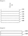
- FIG. 1 is an exemplary diagram illustrating the method.
- the method can comprise a step of irradiating an optical laminate including a first base film (101), a first adhesive layer (201), a linear polarizer (300), a second adhesive layer (202), a second base film (102) and a reverse dispersion liquid crystal layer (400) sequentially with ultraviolet rays (UV).
- a first base film 101
- a first adhesive layer 201
- a linear polarizer 300
- second adhesive layer 202
- second base film 102
- a reverse dispersion liquid crystal layer 400
- an object comprising the first adhesive layer and the second adhesive layer in an uncured state before the ultraviolet ray irradiation can be referred to as an optical laminate
- an object comprising the first adhesive layer and the second adhesive layer in a cured state can be referred to as a polarizing plate. That is, the object in which the first adhesive layer and the second adhesive layer are cured by irradiating the optical laminate with ultraviolet rays can be referred to as a polarizing plate.
- the reverse dispersion liquid crystal layer can have low transmittance for ultraviolet rays due to the inherent characteristics of the reverse dispersion liquid crystals.
- the second base film on which the reverse dispersion liquid crystal layer is formed can have lower transmittance at a wavelength of 400nm, as compared to the first base film.
- the ultraviolet rays having a main emission wavelength band of 380nm to 410nm are irradiated in the direction of the first base film, and thus the ultraviolet rays are irradiated to the opposite side with higher transmittance in the wavelength band than the reverse dispersion liquid crystal layer, whereby it can be advantageous in terms of securing sufficient adhesive force between the base film and the linear polarizer because the first adhesive and the second adhesive can be cured.
- the ultraviolet rays can be irradiated in the direction of the first base film in the optical laminate.
- the main emission wavelength band of the ultraviolet can be a wavelength band of 380nm to 410nm.
- the fact that the main emission wavelength band is a wavelength band of 380nm to 410nm can mean that the energy of light emitted in the entire emission spectrum (200nm to 450nm) for the wavelength is 150W (watt) or more in the wavelength band of the relevant range.
- the first adhesive layer and the second adhesive layer can each comprise a photosensitizer to initiate a curing reaction in a wavelength band of 350nm to 410nm.
- a photosensitizer initiates a curing reaction in a wavelength band of 350nm to 410nm can mean that in the entire absorption spectrum of the photosensitizer, it has at least one absorption maximum wavelength (peak) in the wavelength band of the relevant range.
- polarizer means a film, sheet or element itself having a polarizing function
- polarizing plate means an object comprising the polarizer and another element laminated on one or both sides of the polarizer.
- another element can be exemplified by a protective film of a polarizer, an antireflection film, a retardation film, a pressure-sensitive adhesive layer, an adhesive layer, a surface treatment layer, a liquid crystal layer, a retardation layer or a barrier film, and the like.
- the linear polarizer can be an absorbing polarizer.
- the absorbing polarizer means an element exhibiting selective transmission and absorption characteristics with respect to incident light.
- the absorbing polarizer can transmit light that vibrates in one direction from incident light that vibrates in various directions, and absorb light that vibrates in the other directions.
- the linear polarizer means a case where the selectively transmitting light is linearly polarized light that vibrates in any one direction, and the selectively absorbing light is linearly polarized light that vibrates in a direction orthogonal to the vibration direction of the linearly polarized light.
- the linear polarizer can be a polymer film comprising a dichroic material.
- the dichroic material can be iodine or a dichroic dye.
- As the polymer film a polyvinyl alcohol-based film can be used.
- the dichroic material can be included in the polymer film in an oriented state.
- the linear polarizer and the first base film can be attached via a first adhesive layer. At this time, one side of the first adhesive layer can contact the first base film and the other side can contact the linear polarizer.
- the linear polarizer and the second base film can be attached via a second adhesive layer. At this time, one side of the second adhesive layer can contact the second base film and the other side can contact the linear polarizer.
- the first adhesive layer and the second adhesive layer can be an ultraviolet curable adhesive.
- the ultraviolet curable adhesive can mean an adhesive capable of exhibiting adhesiveness by initiating a curing reaction by irradiation of ultraviolet rays.
- the ultraviolet rays can mean light having a wavelength in the range of about 380nm to 410nm.
- the first adhesive layer and the second adhesive layer can be cured through ultraviolet irradiation.
- the photosensitizer included in each of the first adhesive layer and the second adhesive layer can initiate a curing reaction in a wavelength band of 350nm to 410nm. That is, the photosensitizer can serve as a photoinitiator. Through this, the first adhesive layer and the second adhesive layer can be each cured in the wavelength band of 350nm to 410nm.
- the photosensitizer absorbs light in the wavelength range of 350nm to 410nm, and is a kind of catalyst in a photochemical reaction.
- the photosensitizer can absorb the light having a predetermined wavelength to be in an exited state, and then cause a reaction on a substrate.
- the photosensitizer can include carbonyl compounds, organic sulfur compounds, persulfides, redox compounds, azo and diazo compounds, halogen compounds and photoreducing dyes, and the like, and more specifically, can include benzophenone derivatives such as 2,4-dichlorobenzophenone, methyl o-benzoylbenzoate, 4,4'-bis(dimethylamino)benzophenone and 4,4'-bis(diethylamino)benzophenone; thioxanthone derivatives such as 2-chlorothioxanthone and 2-isopropyl thioxanthone; anthraquinone derivatives such as 2-chloroanthraquinone and 2-methylanthraquinone, and the like.
- benzophenone derivatives such as 2,4-dichlorobenzophenone, methyl o-benzoylbenzoate, 4,4'-bis(dimethylamino)benzophenone and 4,4'-
- the first adhesive layer and the second adhesive layer can each comprise an ultraviolet curable resin.
- the ultraviolet curable resin can include an epoxy-based resin or an acrylic resin. According to one example of the present application, an epoxy-based resin can be used as the ultraviolet curable resin.
- the first adhesive layer and the second adhesive layer can each comprise the photosensitizer in a ratio within a range of 1wt% to 5wt%. If the content of the photosensitizer is too small, it may not be cured, whereas if it is too large, the photosensitizer can be precipitated, thereby resulting in poor appearance in the state of the polarizing plate and causing color change of the polarizing plate to be manufactured, and thus the content of the photosensitizer can be appropriately within the above range.
- the thicknesses of the first adhesive layer and the second adhesive layer can be each in a range of 1 ⁇ m to 5 ⁇ m. If the thickness of the adhesive layer is too thin, the thickness of the coating surface can be uneven, thereby resulting in adhesive-uncoated areas and adhesive force deterioration in certain areas, whereas if it is too thick, the adhesive may not be sufficiently cured and can be vulnerable to durability, and thus the thicknesses of the first adhesive layer and the second adhesive layer can be appropriately in the above range.
- a plastic film can be used for rollable characteristics.
- the plastic film for example, PA (polyacrylate); COP (cyclo olefin polymer); PMMA (poly(methyl methacrylate)); PC (polycarbonate); PE (polyethylene); PP (polypropylene); PVA (polyvinyl alcohol); DAC (diacetyl cellulose); PES (polyethersulfone); PEEK (polyetheretherketone); PPS (polyphenylsulfone), PEI (polyetherimide); PEN (polyethylenemaphthatlate); PET (polyethyleneterephtalate); PI (polyimide); PSF (polysulfone); PAR (polyarylate), and the like can be used.
- PA polyacrylate
- COP cyclo olefin polymer
- PMMA poly(methyl methacrylate)
- PC polycarbonate
- PE polyethylene
- PP polypropylene
- PVA polyviny
- the first base film and the second base film can each exhibit optical isotropy.
- absolute values of a planar phase difference value and a thickness direction phase difference value of the base film can be each 10 nm or less.
- the polarizing plate can prevent external light reflection of external light due to the ⁇ /4 phase delay characteristics of the reverse dispersion liquid crystal layer. It is advantageous that the base film exhibits optical isotropy so as not to impair such performance.
- the planar phase difference (Rin) value and the thickness direction phase difference (Rth) value of the base film, the retardation layer, the liquid crystal layer, the retardation film or the like can be calculated by the following Equations 1 and 2, respectively.
- Rin d ⁇ nx ⁇ ny
- Rth d ⁇ nz ⁇ ny
- nx, ny and nz mean refractive indexes in the x-axis, y-axis and z-axis directions of the base film, the retardation layer, the liquid crystal layer, the retardation film or the like, respectively, and d means the thickness of the base film, the retardation layer, the liquid crystal layer, the retardation film or the like.
- the x-axis means the direction parallel to the in-plane slow axis
- the y-axis means the direction parallel to the in-plane fast axis
- the z-axis means the thickness direction.
- the x and y axes can be perpendicular to each other in the plane.
- the Rin value, the Rth value and the refractive index are described, they mean the Rin value, the Rth value and the refractive index for light having a wavelength of about 550 nm, unless otherwise specified.
- the first base film can have an ultraviolet blocking function.
- the first base film can comprise an ultraviolet absorber.
- the first base film has an ultraviolet blocking function, it is possible to prevent deterioration of an element due to ultraviolet rays.
- the first base film on the side irradiated with ultraviolet rays comprises an ultraviolet absorber, the light in the ultraviolet wavelength band can be blocked partly by the ultraviolet absorber, but as compared to irradiating the reverse dispersion liquid crystal layer side of the second base film with ultraviolet rays, it has higher transmittance for ultraviolet rays in the wavelength band of 380nm to 410nm, so that it can be advantageous in terms of curing of the first adhesive layer and the second adhesive layer.
- the first base film can have transmittance of 65% or more at a wavelength of 400nm. As the wavelength decreases, the transmittance decreases rapidly, which can be less than 10% at a wavelength of 380nm.
- the upper limit of the transmittance of the first base film at a wavelength of 400nm can be, for example, less than 90%. Such transmittance characteristics can be attributable to characteristics of an ultraviolet blocker to be described below.
- the second base film on which the reverse dispersion liquid crystal layer is formed can have transmittance of less than 40% at a wavelength of 400nm. As the wavelength decreases, the transmittance decreases rapidly, which can be less than 3% at a wavelength of 380nm. This transmittance characteristics are attributable to the inherent characteristics of the reverse dispersion liquid crystal.
- the thickness of the first base film and/or the second base film can be, for example, 10 ⁇ m to 100 ⁇ m.
- the thickness of the base film is within the above range, it can be advantageous for the thinning of the polarizing plate and the implementation of rollable characteristics.
- the reverse dispersion liquid crystal layer can be in contact with the opposite side on which the second adhesive layer of the second base film exists.
- the reverse dispersion liquid crystal layer can mean a liquid crystal layer satisfying the following equation 3.
- the desired phase delay characteristics can be exhibited in a wide visible light range, so that it can be advantageous to exhibit antireflection performance in a wide visible light range.
- R ( ⁇ ) is the planar phase difference value of the liquid crystal layer for a wavelength of ⁇ nm.
- the reverse dispersion liquid crystal layer can comprise a reverse dispersion liquid crystal compound.
- the reverse dispersion liquid crystal compound can mean a liquid crystal compound in which the liquid crystal layer formed by curing the liquid crystal compound alone shows reverse dispersibility of Equation 3 above.
- the liquid crystal compound can be a polymerizable liquid crystal compound.
- the term "polymerizable liquid crystal compound” can mean a compound containing a site capable of exhibiting liquid crystallinity, for example, a mesogen skeleton or the like, and also containing one or more polymerizable functional groups.
- the polymerizable functional group can be, for example, an alkenyl group, an epoxy group, a carboxyl group, an acryloyl group, a methacryloyl group, an acryloyloxy group or a methacryloyloxy group, but is not limited thereto.
- wavelength dispersibility and phase difference values can mean wavelength dispersibility and phase difference values with respect to the liquid crystal layer formed by curing the liquid crystal compound in a state where the orientation is made on the xy plane, unless otherwise specified.
- the R (450)/R (550) value of the reverse dispersion liquid crystal layer can be, for example, 0.99 or less. In one example, the R (450)/R (550) can be in a range of 0.6 to 0.99.
- the reverse dispersion liquid crystal layer can have an R (650)/R (550) value of 1.01 or more. In one example, the R (650) / R (550) value can be in the range of 1.01 to 1.30.
- the liquid crystal compound having the R (450)/R (550) and/or R (650)/R (550) values is not particularly limited.
- liquid crystal compounds having R (450)/R (550) and/or R (650)/R (550) in the above ranges as liquid crystal compounds having reverse dispersibility are known, and such liquid crystal compounds can be selected and used.
- the phase difference value of the reverse dispersion liquid crystal layer can be appropriately adjusted in consideration of the use that the polarizing plate is applied.
- the planar phase difference value of the reverse dispersion liquid crystal layer for a wavelength of 550nm can be in a range of 100nm to 200nm, 100nm to 180nm, 100nm to 150nm or 130nm to 150nm.
- the angle formed by the slow axis of the reverse dispersion liquid crystal layer and the absorption axis of the linear polarizer can be appropriately adjusted in consideration of the use to which the polarizer is applied.
- the angle formed by the slow axis of the reverse dispersion liquid crystal layer and the absorption axis of the linear polarizer can be in a range of 40 degrees to 50 degrees.
- the optical laminate or the polarizing plate can further comprise a +C plate formed on one side of the reverse dispersion liquid crystal layer.
- the +C plate can mean a retardation layer satisfying the refractive index relationship of Equation 4 below.
- nx, ny and nz mean refractive indexes for a wavelength of 550 nm in the x-axis, y-axis, and z-axis directions of the retardation layer, respectively, and the definitions of the directions of the x-axis, y-axis and z-axis are as described above.
- the polarizing plate manufactured according to the method of the present application can be applied, for example, to rollable OLED panels.
- the rollable OLED panel can exhibit the same phase difference as a -C plate due to the characteristics of the base material, and thus when the optical laminate further comprises a +C plate, it can compensate for the phase difference of the -C plate, so that it can be more advantageous for improving visual appreciation characteristics.
- the thickness direction phase difference value of the +C plate can be, for example, more than 0nm.
- the thickness direction phase difference value of the +C plate can be specifically in a range of 90nm to 110nm. It can be more advantageous to improve the visual appreciation characteristics of the OLED panel within such a thickness direction phase difference value range.
- the ultraviolet light can be irradiated to the first base film side of the optical laminate.
- the ultraviolet rays are irradiated to the second base film side where the reverse dispersion liquid crystal layer is present, most of the light in the ultraviolet long wavelength band is blocked by the reverse dispersion liquid crystal layer so that the adhesive is not cured, and even if it is cured by increasing the ultraviolet intensity, appearance wrinkles are severely generated, whereby there is a problem of difficult commercialization.
- the wavelength of the ultraviolet rays irradiated on the optical laminate can be in the range of 380nm to 410nm.
- the first base film and the second base film block most of the ultraviolet rays, whereby the initiator does not participate in the curing reaction, and when it exceeds the above range, the wavelength light is absorbed into the films as the thermal energy to be capable of applying physical deformation thereto. Therefore, it can be preferable that the ultraviolet wavelength band is adjusted within the above range.
- the light quantity of ultraviolet rays irradiated on the optical laminate can be in a range of 200 mJ to 400 mJ or 250 mJ to 400 mJ.
- the light quantity of ultraviolet rays is adjusted within the above range.
- the method for manufacturing a polarizing plate of the present application can further comprise a step of irradiating the optical laminate with ultraviolet rays and then forming a pressure-sensitive adhesive layer on the reverse dispersion liquid crystal layer side.
- the pressure-sensitive adhesive layer can perform a function of attaching a polarizing plate to an OLED panel.
- a known pressure-sensitive adhesive such as an acryl-based pressure-sensitive adhesive, a silicone-based pressure-sensitive adhesive, a rubber-based pressure-sensitive adhesive and a urethane pressure-sensitive adhesive can be used without any particular limitation.
- the polarizing plate manufactured by the manufacturing method can have excellent water resistance.
- the polarizing plate can have an adhesive force of IN or more as immediately measured after submerging it in water at a temperature of 60°C for 6 hours and then taking it out.
- the term "immediately” can mean within about 3 minutes.
- the polarizing plate can further comprise a surface treatment layer.
- the surface treatment layer can be located on the opposite side where the linear polarizer of the first base film exists.
- the surface treatment layer can include an anti-fog layer, a self-healing layer, an anti-reflection layer, an anti-finger layer, an anti-fouling layer, an anti-glare layer, a mirror layer or a hardness enhancement layer.
- the hardness enhancing layer is also commonly referred to as a "hard coating layer.”
- the material, the formation method, the physical properties, and the like of the surface treatment layer are not particularly limited and the contents known in the art can be applied.
- the polarizing plate can further comprise a barrier film.
- the barrier film can be located on the opposite side where the second base film of the reverse dispersion liquid crystal layer exists.
- the barrier film can comprise a third base film and a barrier layer laminated on the third base film.
- the reverse dispersion liquid crystal layer and the barrier film can be attached via a pressure-sensitive adhesive layer.
- the polarizing plate further comprises a barrier film, it can have excellent barrier performance against external environments such as moisture.
- the third base film can have a water vapor transmission rate in a range of 1 g/m 2 ⁇ day to 100 g/m 2 ⁇ day.
- the first and second base films as mentioned above can be used.
- an acryl-based film or a COP-based film can be used as the third base film.
- the use of such a base film can be advantageous in terms of exhibiting the water vapor transmission rate within the above range.
- the barrier film As the barrier film is formed in a multilayer structure in which a first barrier layer and a second barrier layer are laminated, it can improve barrier performance against external environments such as moisture.
- the water vapor transmission rate of the first barrier layer and the second barrier layer can be 10 -4 g/m 2 ⁇ day to 10 -6 g/m 2 ⁇ day.
- the moisture vapor transmission rate can be a value measured in a state where the first barrier layer and the second barrier layer are laminated.
- the water vapor transmission rate of the first and second barrier layers satisfies the above range, it is possible to effectively protect an OLED element from moisture.
- the water vapor transmission rate exceeds the above range, the moisture can penetrate into the OLED element to cause damage to the OLED element, thereby causing deteriorated black spots.
- the first barrier layer and the second barrier layer can be each an inorganic thin film layer.
- the inorganic thin film layer can comprise, for example, at least one inorganic compound selected from the group consisting of oxides, nitrides, hydrides and composite compounds.
- the element constituting the inorganic compound can be exemplified by silicon (Si), nitrogen (N), aluminum (Al), magnesium (Mg), calcium (Ca), potassium (K), zinc (Zn), tin (Sn), nickel (Ni), sodium (Na), boron (B), titanium (Ti), lead (Pb), zirconium (Zr) or yttrium (Y), and the like.
- the first and second barrier layers can each comprise a SiOxNy compound.
- the SiOxNy compound can be suitable as a material such that the first barrier layer and the second barrier layer exhibit a water vapor transmission rate within the above range.
- the first and second barrier layers can each comprise a SiOxNy compound as a main component.
- the first and second barrier layers can each comprise a SiOxNy compound in a ratio of 80 wt% or more, 85 wt% or more, 90 wt% or more, or 95 wt% or more.
- the SiOxNy compound can be a polysilazane.
- the polysilazane is a kind of silicone compound, which can mean a polymer having a skeleton of Si-N bonds.
- the polysilazane can be a polymer comprising "-(SiR 1 R 2 -NR 3 )-" as a repeating unit.
- the R 1 , R 2 and R 3 can be each independently a hydrogen atom, an oxygen atom or an organic substituent.
- one or more of R 1 , R 2 and R 3 can comprise an oxygen atom.
- the first and second barrier layers can each comprise a SiOxNy compound, which is subjected to modification treatment, for example, plasma treatment, as described below.
- the first barrier layer and the second barrier layer can each have a thickness in a range of 50nm to 200nm.
- the thicknesses of the first barrier layer and the second barrier layer are within the above range, it can be advantageous to implement water vapor transmission rate within the above range, thinning of the polarizing plate, and rollable characteristics.
- the present application relates to a use of the polarizing plate.
- the polarizer can be applied to an organic light emitting display device.
- FIG 2 illustratively shows an organic light emitting display device to which the polarizing plate is applied.
- the organic light emitting display device can comprise an organic light emitting display panel (1000) and the polarizing plate (2000) arranged on one side of the organic light emitting display panel (1000).
- the reverse dispersion liquid crystal layer can be arranged closer to the organic light emitting display panel as compared to the linear polarizer of the polarizing plate.
- the organic light emitting display panel can comprise a base substrate, a lower electrode, a light emitting layer including an organic material, and an upper electrode. If necessary, an encapsulation substrate can be further formed on the upper electrode.
- the anode is an electrode to which holes are injected, which can be made of a conductive material having a high work function
- the cathode is an electrode to which electrons are injected, which can be made of a conductive material having a low work function.
- At least one can be made of a transparent conductive material through which the emitted light can be emitted to the outside, in which the material can be, for example, ITO (indium tin oxide) or IZO (indium zinc oxide).
- the organic light emitting layer can comprise an organic material capable of emitting light when a voltage has been applied to the lower electrode and the upper electrode.
- Sub-layers can be further included between the lower electrode and the organic light emitting layer and between the upper electrode and the organic light emitting layer.
- the sublayer can include a hole transporting layer, a hole injecting layer, an electron injecting layer and/or an electron transporting layer for balancing electrons and holes, but is not limited thereto.
- the encapsulation substrate can be made of glass, a metal and/or a polymer, and can encapsulate the lower electrode layer, the organic light emitting layer and the upper electrode layer to prevent moisture and/or oxygen from being introduced from the outside.
- the polarizing plate can be arranged on the side where light is emitted from the organic light emitting display panel.
- a bottom emission structure in which light is emitted toward the base substrate it can be arranged outside the base substrate
- a top emission structure in which light is emitted toward the encapsulation substrate it can be arranged outside the encapsulation substrate.
- the polarizing plate manufactured according to the method of the present application can exhibit excellent anti-reflection functions within a wide visible light range, can exhibit sufficient adhesive force between the base film and the linear polarizer, has excellent water resistance, and can be thinned and rolled.
- Such a polarizing plate can be applied to an organic light emitting display device, thereby improving black visual appreciation, improving durability, miniaturizing the device, and implementing a rollable device.
- the present application provides a method for manufacturing a polarizing plate, which can exhibit excellent anti-reflection functions within a wide visible light range, can exhibit sufficient adhesive force between a base film and a linear polarizer, has excellent water resistance and is capable of thinning and rolling.
- the polarizing plate can be applied to an organic light emitting display device, thereby improving black visual appreciation, improving durability, miniaturizing the device, and implementing a rollable device.
- a PVA-based linear polarizer was manufactured by a wet stretching method (using the product name M6000L base material from Nippon gosei).
- a first adhesive layer having a thickness of 2 ⁇ m in an uncured state was formed on one side of a first base film (UZ TAC, Fuji product) having a thickness of 60 ⁇ m.
- the first base film comprises an ultraviolet absorber and has transmittance of about 77% at a wavelength of 400nm and transmittance of about 4% at a wavelength of 380nm.
- the first adhesive comprises a photosensitizer (DETX-S manufacturer: IHT), which initiates a curing reaction in a wavelength band of 350 nm to 410 nm to an epoxy-based UV curable resin, in an amount of 2wt%.
- Reverse dispersion liquid crystals (LG Chemical) were coated on one side of a second base film (Zero Retardation TAC, Konica product) having a thickness of 40 ⁇ m to form a reverse dispersion liquid crystal layer having a planar phase difference value of 142nm for a wavelength of 550nm.
- the second base film on which the reverse dispersion liquid crystal layer has been formed has transmittance of about 27% at a wavelength of 400nm and transmittance of about 0.7% at a wavelength of 380nm.
- a second adhesive layer having a thickness of 2 ⁇ m in an uncured state was formed on the opposite side of the second base film on which the reverse dispersion liquid crystal layer was formed.
- the second adhesive comprises a photosensitizer (DETX-S manufacturer: IHT), which initiates a curing reaction in a wavelength band of 350nm to 410nm to an epoxy-based UV curable resin, in an amount of 2wt%.
- the first base film was attached to one side of the linear polarizer via the first adhesive layer.
- the second base film on which the reverse dispersion liquid crystal layer was formed was attached to the side of the linear polarizer to which the first base film was not attached via the second adhesive layer. At this time, they were attached such that the angle formed by the light absorption axis of the linear polarizer and the slow axis of the reverse dispersion liquid crystal layer was 45 degrees.
- an optical laminate comprising the first base film, the first adhesive layer, the linear polarizer, the second adhesive layer, the second base film and the reverse dispersion liquid crystal layer sequentially was provided.
- a polarizing plate was manufactured by irradiating the first base film side of the optical laminate with ultraviolet rays having a main emission wavelength of 380 nm to 410 nm at a light quantity of 250 mJ by using ultraviolet light emitting equipment (electrodeless type UV curing machine) and curing the first adhesive and the second adhesive.
- a polarizing plate was manufactured in the same manner as in Example 1, except that the first adhesive layer and the second adhesive layer were cured by the following method.
- adhesive layers having a thickness of 100nm in an uncured state were formed by using a water-based adhesive (product name: Z3, manufacturer: LG Chemical) containing a polyvinyl alcohol resin (there was no photosensitizer in the water-based adhesive), and cured by a thermosetting method (90°C, 2 minutes).
- a polarizing plate was manufactured in the same manner as in Example 1, except that the ultraviolet rays were irradiated to the reverse dispersion liquid crystal layer side instead of the first base film side in Example 1.
- a polarizing plate was manufactured in the same manner as in Example 1, except that the ultraviolet rays were irradiated to the reverse dispersion liquid crystal layer side instead of the first base film side in Example 1, and the light quantity of ultraviolet rays was changed to 900 mJ.
- the manufactured polarizing plate sample was cut to a size of 20mm ⁇ 150mm and the surface to be peeled is placed down and attached to the peeling machine substrate without foaming with a double-sided tape, and then the film opposite to the PVA was peeled off by 90 degrees at a rate of 300 mm/min to measure the adhesive force (unit N/20mm).
- the adhesive force measurement equipment was a TA.XT texture analyzer.
- the initial adhesive force means the adhesive force measured at a temperature of 25°C.
- the manufactured polarizing plate was submerged in water at 60°C for 6 hours and then taken out, and the adhesive force was immediately measured to evaluate water resistance.
- the cured adhesive surface was rubbed by hand, and the curing degree was evaluated based on the following criteria.
- the initial adhesive force is in the same level as IN or more, but in the water resistance evaluation, the adhesive force of Comparative Example 1 is reduced to less than IN, so that it can be seen that it is vulnerable to water resistance.
- the bottom base material surface (ZRT + liquid crystal) of Comparative Example 2 has been irradiated with UV rays and the adhesive has not been sufficiently cured due to the low transmittance of the bottom base material surface in the wavelength range of 400nm or less as compared to the top base material surface, and as shown in Comparative Example 3, even if the light quantity of UV rays is increased 3 times or more as compared to Example 1, it can be seen that the adhesive force is reduced due to incomplete curing.
- first base film 102 second base film 201: first adhesive layer 202: second adhesive layer 300: linear polarizer 400: reverse dispersion liquid crystal layer 1000: organic light emitting display panel 2000: polarizing plate
Landscapes
- Physics & Mathematics (AREA)
- Engineering & Computer Science (AREA)
- General Physics & Mathematics (AREA)
- Optics & Photonics (AREA)
- Health & Medical Sciences (AREA)
- Manufacturing & Machinery (AREA)
- Ophthalmology & Optometry (AREA)
- Mechanical Engineering (AREA)
- Chemical & Material Sciences (AREA)
- Crystallography & Structural Chemistry (AREA)
- Polarising Elements (AREA)
- Electroluminescent Light Sources (AREA)
- Laminated Bodies (AREA)
- Adhesive Tapes (AREA)
- Adhesives Or Adhesive Processes (AREA)
Abstract
Description
- The present application relates to a method for manufacturing a polarizing plate.
- The present application claims the benefit of priority based on
Korean Patent Application No. 10-2019-0019179 filed on February 19, 2019 - OLED (organic light emitting device) panels have high external reflection due to electrode exposure, whereby polarizers are used for anti-reflection functions. The polarizing plate implementing anti-reflection functions basically requires linear and circular polarizers in the structure. At this time, since the panel black visual appreciation depends on the material characteristics of the circular polarizer, the selection of the circular polarizer is a very important factor in the polarizing plate.
- For example, in order to implement the perfect black visual appreciation, the use of reverse dispersion materials is required so that the circular polarizer has a λ/4 phase difference at all wavelengths of visible light.
- In attaching the reverse dispersion liquid crystal type polarizer to the linear polarizer, when an ultraviolet curable adhesive is used, it can be advantageous in terms of the water resistance of the polarizing plate, but the curing does not sufficiently occur by blocking the transmissive ultraviolet rays due to the inherent characteristics of the reverse dispersion liquid crystals, so that there is a problem that the adhesive force is lowered.
- As an alternative, it can be considered to use a water-based adhesive, but when the water-based adhesive is used, there is a problem that it has weak water resistance and is vulnerable to high-humidity external environments. As another alternative, a method of attaching the reverse dispersion liquid crystal type circular polarizer to a general polarizing plate with a pressure-sensitive adhesive can be considered, but there is a disadvantage that the thickness becomes thick and the number of processes increases (Patent Document 1:
Korean Laid-Open Patent Publication No. 2009-0122138 - The present application provides a method for manufacturing a polarizing plate, which can exhibit excellent anti-reflection functions within a wide visible light range, can exhibit sufficient adhesive force between a base film and a linear polarizer, has excellent water resistance and is capable of thinning and rolling, and a use of the polarizing plate.
- The present application relates to a method for manufacturing a polarizing plate.
Figure 1 is an exemplary diagram illustrating the method. As shown inFigure 1 , the method can comprise a step of irradiating an optical laminate including a first base film (101), a first adhesive layer (201), a linear polarizer (300), a second adhesive layer (202), a second base film (102) and a reverse dispersion liquid crystal layer (400) sequentially with ultraviolet rays (UV). - In this specification, in order to distinguish objects before and after the ultraviolet rays are irradiated, an object comprising the first adhesive layer and the second adhesive layer in an uncured state before the ultraviolet ray irradiation can be referred to as an optical laminate, and an object comprising the first adhesive layer and the second adhesive layer in a cured state can be referred to as a polarizing plate. That is, the object in which the first adhesive layer and the second adhesive layer are cured by irradiating the optical laminate with ultraviolet rays can be referred to as a polarizing plate.
- The reverse dispersion liquid crystal layer can have low transmittance for ultraviolet rays due to the inherent characteristics of the reverse dispersion liquid crystals. In one example, the second base film on which the reverse dispersion liquid crystal layer is formed can have lower transmittance at a wavelength of 400nm, as compared to the first base film. According to the present application, the ultraviolet rays having a main emission wavelength band of 380nm to 410nm are irradiated in the direction of the first base film, and thus the ultraviolet rays are irradiated to the opposite side with higher transmittance in the wavelength band than the reverse dispersion liquid crystal layer, whereby it can be advantageous in terms of securing sufficient adhesive force between the base film and the linear polarizer because the first adhesive and the second adhesive can be cured.
- Hereinafter, the method for manufacturing a polarizing plate of the present application will be described in detail.
- The ultraviolet rays can be irradiated in the direction of the first base film in the optical laminate. The main emission wavelength band of the ultraviolet can be a wavelength band of 380nm to 410nm. In this specification, the fact that the main emission wavelength band is a wavelength band of 380nm to 410nm can mean that the energy of light emitted in the entire emission spectrum (200nm to 450nm) for the wavelength is 150W (watt) or more in the wavelength band of the relevant range.
- The first adhesive layer and the second adhesive layer can each comprise a photosensitizer to initiate a curing reaction in a wavelength band of 350nm to 410nm. In this specification, the fact that a photosensitizer initiates a curing reaction in a wavelength band of 350nm to 410nm can mean that in the entire absorption spectrum of the photosensitizer, it has at least one absorption maximum wavelength (peak) in the wavelength band of the relevant range.
- In this specification, the terms, polarizer and polarizing plate, refer to objects that are distinguished from each other. The term polarizer means a film, sheet or element itself having a polarizing function, and the term polarizing plate means an object comprising the polarizer and another element laminated on one or both sides of the polarizer. Here, another element can be exemplified by a protective film of a polarizer, an antireflection film, a retardation film, a pressure-sensitive adhesive layer, an adhesive layer, a surface treatment layer, a liquid crystal layer, a retardation layer or a barrier film, and the like.
- The linear polarizer can be an absorbing polarizer. In this specification, the absorbing polarizer means an element exhibiting selective transmission and absorption characteristics with respect to incident light. For example, the absorbing polarizer can transmit light that vibrates in one direction from incident light that vibrates in various directions, and absorb light that vibrates in the other directions.
- In this specification, the linear polarizer means a case where the selectively transmitting light is linearly polarized light that vibrates in any one direction, and the selectively absorbing light is linearly polarized light that vibrates in a direction orthogonal to the vibration direction of the linearly polarized light.
- The linear polarizer can be a polymer film comprising a dichroic material. The dichroic material can be iodine or a dichroic dye. As the polymer film, a polyvinyl alcohol-based film can be used. The dichroic material can be included in the polymer film in an oriented state.
- In the optical laminate, the linear polarizer and the first base film can be attached via a first adhesive layer. At this time, one side of the first adhesive layer can contact the first base film and the other side can contact the linear polarizer.
- In the optical laminate, the linear polarizer and the second base film can be attached via a second adhesive layer. At this time, one side of the second adhesive layer can contact the second base film and the other side can contact the linear polarizer.
- The first adhesive layer and the second adhesive layer can be an ultraviolet curable adhesive. In this specification, the ultraviolet curable adhesive can mean an adhesive capable of exhibiting adhesiveness by initiating a curing reaction by irradiation of ultraviolet rays. In this specification, the ultraviolet rays can mean light having a wavelength in the range of about 380nm to 410nm. In one example, the first adhesive layer and the second adhesive layer can be cured through ultraviolet irradiation. In the present application, it is possible to secure excellent water resistance by using the ultraviolet curable adhesive instead of the water-based adhesive. Therefore, the polarizing plate manufactured according to the method of the present application can exhibit excellent durability even in high-humidity external environments.
- As described above, the photosensitizer included in each of the first adhesive layer and the second adhesive layer can initiate a curing reaction in a wavelength band of 350nm to 410nm. That is, the photosensitizer can serve as a photoinitiator. Through this, the first adhesive layer and the second adhesive layer can be each cured in the wavelength band of 350nm to 410nm.
- The photosensitizer absorbs light in the wavelength range of 350nm to 410nm, and is a kind of catalyst in a photochemical reaction. The photosensitizer can absorb the light having a predetermined wavelength to be in an exited state, and then cause a reaction on a substrate.
- An example of the photosensitizer can include carbonyl compounds, organic sulfur compounds, persulfides, redox compounds, azo and diazo compounds, halogen compounds and photoreducing dyes, and the like, and more specifically, can include benzophenone derivatives such as 2,4-dichlorobenzophenone, methyl o-benzoylbenzoate, 4,4'-bis(dimethylamino)benzophenone and 4,4'-bis(diethylamino)benzophenone; thioxanthone derivatives such as 2-chlorothioxanthone and 2-isopropyl thioxanthone; anthraquinone derivatives such as 2-chloroanthraquinone and 2-methylanthraquinone, and the like.
- The first adhesive layer and the second adhesive layer can each comprise an ultraviolet curable resin. The ultraviolet curable resin can include an epoxy-based resin or an acrylic resin. According to one example of the present application, an epoxy-based resin can be used as the ultraviolet curable resin.
- The first adhesive layer and the second adhesive layer can each comprise the photosensitizer in a ratio within a range of 1wt% to 5wt%. If the content of the photosensitizer is too small, it may not be cured, whereas if it is too large, the photosensitizer can be precipitated, thereby resulting in poor appearance in the state of the polarizing plate and causing color change of the polarizing plate to be manufactured, and thus the content of the photosensitizer can be appropriately within the above range.
- The thicknesses of the first adhesive layer and the second adhesive layer can be each in a range of 1µm to 5µm. If the thickness of the adhesive layer is too thin, the thickness of the coating surface can be uneven, thereby resulting in adhesive-uncoated areas and adhesive force deterioration in certain areas, whereas if it is too thick, the adhesive may not be sufficiently cured and can be vulnerable to durability, and thus the thicknesses of the first adhesive layer and the second adhesive layer can be appropriately in the above range.
- As the first base film and/or the second base film, a plastic film can be used for rollable characteristics. As the plastic film, for example, PA (polyacrylate); COP (cyclo olefin polymer); PMMA (poly(methyl methacrylate)); PC (polycarbonate); PE (polyethylene); PP (polypropylene); PVA (polyvinyl alcohol); DAC (diacetyl cellulose); PES (polyethersulfone); PEEK (polyetheretherketone); PPS (polyphenylsulfone), PEI (polyetherimide); PEN (polyethylenemaphthatlate); PET (polyethyleneterephtalate); PI (polyimide); PSF (polysulfone); PAR (polyarylate), and the like can be used.
- The first base film and the second base film can each exhibit optical isotropy. In one example, absolute values of a planar phase difference value and a thickness direction phase difference value of the base film can be each 10 nm or less. As described below, the polarizing plate can prevent external light reflection of external light due to the λ/4 phase delay characteristics of the reverse dispersion liquid crystal layer. It is advantageous that the base film exhibits optical isotropy so as not to impair such performance.
- In this specification, the planar phase difference (Rin) value and the thickness direction phase difference (Rth) value of the base film, the retardation layer, the liquid crystal layer, the retardation film or the like can be calculated by the following Equations 1 and 2, respectively.


- In Equations 1 and 2, nx, ny and nz mean refractive indexes in the x-axis, y-axis and z-axis directions of the base film, the retardation layer, the liquid crystal layer, the retardation film or the like, respectively, and d means the thickness of the base film, the retardation layer, the liquid crystal layer, the retardation film or the like. The x-axis means the direction parallel to the in-plane slow axis, the y-axis means the direction parallel to the in-plane fast axis, and the z-axis means the thickness direction. The x and y axes can be perpendicular to each other in the plane. In this specification, while the Rin value, the Rth value and the refractive index are described, they mean the Rin value, the Rth value and the refractive index for light having a wavelength of about 550 nm, unless otherwise specified.
- The first base film can have an ultraviolet blocking function. The first base film can comprise an ultraviolet absorber. When the first base film has an ultraviolet blocking function, it is possible to prevent deterioration of an element due to ultraviolet rays. When the first base film on the side irradiated with ultraviolet rays comprises an ultraviolet absorber, the light in the ultraviolet wavelength band can be blocked partly by the ultraviolet absorber, but as compared to irradiating the reverse dispersion liquid crystal layer side of the second base film with ultraviolet rays, it has higher transmittance for ultraviolet rays in the wavelength band of 380nm to 410nm, so that it can be advantageous in terms of curing of the first adhesive layer and the second adhesive layer.
- The first base film can have transmittance of 65% or more at a wavelength of 400nm. As the wavelength decreases, the transmittance decreases rapidly, which can be less than 10% at a wavelength of 380nm. The upper limit of the transmittance of the first base film at a wavelength of 400nm can be, for example, less than 90%. Such transmittance characteristics can be attributable to characteristics of an ultraviolet blocker to be described below.
- The second base film on which the reverse dispersion liquid crystal layer is formed can have transmittance of less than 40% at a wavelength of 400nm. As the wavelength decreases, the transmittance decreases rapidly, which can be less than 3% at a wavelength of 380nm. This transmittance characteristics are attributable to the inherent characteristics of the reverse dispersion liquid crystal.
- The thickness of the first base film and/or the second base film can be, for example, 10µm to 100µm. When the thickness of the base film is within the above range, it can be advantageous for the thinning of the polarizing plate and the implementation of rollable characteristics.
- The reverse dispersion liquid crystal layer can be in contact with the opposite side on which the second adhesive layer of the second base film exists. In this specification, the reverse dispersion liquid crystal layer can mean a liquid crystal layer satisfying the following equation 3. In the case of using the reverse dispersion liquid crystal layer, the desired phase delay characteristics can be exhibited in a wide visible light range, so that it can be advantageous to exhibit antireflection performance in a wide visible light range.

- In Equation 3, R (λ) is the planar phase difference value of the liquid crystal layer for a wavelength of λnm.
- The reverse dispersion liquid crystal layer can comprise a reverse dispersion liquid crystal compound. In this specification, the reverse dispersion liquid crystal compound can mean a liquid crystal compound in which the liquid crystal layer formed by curing the liquid crystal compound alone shows reverse dispersibility of Equation 3 above.
- In one example, the liquid crystal compound can be a polymerizable liquid crystal compound. In this specification, the term "polymerizable liquid crystal compound" can mean a compound containing a site capable of exhibiting liquid crystallinity, for example, a mesogen skeleton or the like, and also containing one or more polymerizable functional groups. The polymerizable functional group can be, for example, an alkenyl group, an epoxy group, a carboxyl group, an acryloyl group, a methacryloyl group, an acryloyloxy group or a methacryloyloxy group, but is not limited thereto.
- In this specification, while the wavelength dispersibility and phase difference values are described, they can mean wavelength dispersibility and phase difference values with respect to the liquid crystal layer formed by curing the liquid crystal compound in a state where the orientation is made on the xy plane, unless otherwise specified.
- The R (450)/R (550) value of the reverse dispersion liquid crystal layer can be, for example, 0.99 or less. In one example, the R (450)/R (550) can be in a range of 0.6 to 0.99. The reverse dispersion liquid crystal layer can have an R (650)/R (550) value of 1.01 or more. In one example, the R (650) / R (550) value can be in the range of 1.01 to 1.30.
- The liquid crystal compound having the R (450)/R (550) and/or R (650)/R (550) values is not particularly limited. In this field, liquid crystal compounds having R (450)/R (550) and/or R (650)/R (550) in the above ranges as liquid crystal compounds having reverse dispersibility are known, and such liquid crystal compounds can be selected and used.
- The phase difference value of the reverse dispersion liquid crystal layer can be appropriately adjusted in consideration of the use that the polarizing plate is applied. The planar phase difference value of the reverse dispersion liquid crystal layer for a wavelength of 550nm can be in a range of 100nm to 200nm, 100nm to 180nm, 100nm to 150nm or 130nm to 150nm.
- The angle formed by the slow axis of the reverse dispersion liquid crystal layer and the absorption axis of the linear polarizer can be appropriately adjusted in consideration of the use to which the polarizer is applied. The angle formed by the slow axis of the reverse dispersion liquid crystal layer and the absorption axis of the linear polarizer can be in a range of 40 degrees to 50 degrees.
- The optical laminate or the polarizing plate can further comprise a +C plate formed on one side of the reverse dispersion liquid crystal layer. In this specification, the +C plate can mean a retardation layer satisfying the refractive index relationship of Equation 4 below.

- In Equation 4, nx, ny and nz mean refractive indexes for a wavelength of 550 nm in the x-axis, y-axis, and z-axis directions of the retardation layer, respectively, and the definitions of the directions of the x-axis, y-axis and z-axis are as described above.
- The polarizing plate manufactured according to the method of the present application can be applied, for example, to rollable OLED panels. The rollable OLED panel can exhibit the same phase difference as a -C plate due to the characteristics of the base material, and thus when the optical laminate further comprises a +C plate, it can compensate for the phase difference of the -C plate, so that it can be more advantageous for improving visual appreciation characteristics.
- The thickness direction phase difference value of the +C plate can be, for example, more than 0nm. The thickness direction phase difference value of the +C plate can be specifically in a range of 90nm to 110nm. It can be more advantageous to improve the visual appreciation characteristics of the OLED panel within such a thickness direction phase difference value range.
- As described above, the ultraviolet light can be irradiated to the first base film side of the optical laminate. When the ultraviolet rays are irradiated to the second base film side where the reverse dispersion liquid crystal layer is present, most of the light in the ultraviolet long wavelength band is blocked by the reverse dispersion liquid crystal layer so that the adhesive is not cured, and even if it is cured by increasing the ultraviolet intensity, appearance wrinkles are severely generated, whereby there is a problem of difficult commercialization.
- The wavelength of the ultraviolet rays irradiated on the optical laminate can be in the range of 380nm to 410nm. When the ultraviolet wavelength is less than the above range, the first base film and the second base film block most of the ultraviolet rays, whereby the initiator does not participate in the curing reaction, and when it exceeds the above range, the wavelength light is absorbed into the films as the thermal energy to be capable of applying physical deformation thereto. Therefore, it can be preferable that the ultraviolet wavelength band is adjusted within the above range.
- The light quantity of ultraviolet rays irradiated on the optical laminate can be in a range of 200 mJ to 400 mJ or 250 mJ to 400 mJ. When the light quantity of ultraviolet rays is too small, the curing may not occur sufficiently, and when the light quantity of ultraviolet rays is too large, physical deformation is caused in the polarizing plate and wrinkles are severely generated in appearance, whereby the commercialization can be difficult. Therefore, it can be preferable that the light quantity of ultraviolet rays is adjusted within the above range.
- The method for manufacturing a polarizing plate of the present application can further comprise a step of irradiating the optical laminate with ultraviolet rays and then forming a pressure-sensitive adhesive layer on the reverse dispersion liquid crystal layer side. The pressure-sensitive adhesive layer can perform a function of attaching a polarizing plate to an OLED panel. As the pressure-sensitive adhesive layer, a known pressure-sensitive adhesive such as an acryl-based pressure-sensitive adhesive, a silicone-based pressure-sensitive adhesive, a rubber-based pressure-sensitive adhesive and a urethane pressure-sensitive adhesive can be used without any particular limitation.
- The polarizing plate manufactured by the manufacturing method can have excellent water resistance. In one example, the polarizing plate can have an adhesive force of IN or more as immediately measured after submerging it in water at a temperature of 60°C for 6 hours and then taking it out. In this specification, the term "immediately" can mean within about 3 minutes.
- The polarizing plate can further comprise a surface treatment layer. The surface treatment layer can be located on the opposite side where the linear polarizer of the first base film exists. The surface treatment layer can include an anti-fog layer, a self-healing layer, an anti-reflection layer, an anti-finger layer, an anti-fouling layer, an anti-glare layer, a mirror layer or a hardness enhancement layer. In the art, the hardness enhancing layer is also commonly referred to as a "hard coating layer." The material, the formation method, the physical properties, and the like of the surface treatment layer are not particularly limited and the contents known in the art can be applied.
- The polarizing plate can further comprise a barrier film. The barrier film can be located on the opposite side where the second base film of the reverse dispersion liquid crystal layer exists. The barrier film can comprise a third base film and a barrier layer laminated on the third base film. The reverse dispersion liquid crystal layer and the barrier film can be attached via a pressure-sensitive adhesive layer. When the polarizing plate further comprises a barrier film, it can have excellent barrier performance against external environments such as moisture.
- The third base film can have a water vapor transmission rate in a range of 1 g/m2·day to 100 g/m2·day. As the third base film, the first and second base films as mentioned above can be used. In one specific example, an acryl-based film or a COP-based film can be used as the third base film. The use of such a base film can be advantageous in terms of exhibiting the water vapor transmission rate within the above range.
- As the barrier film is formed in a multilayer structure in which a first barrier layer and a second barrier layer are laminated, it can improve barrier performance against external environments such as moisture. In one example, the water vapor transmission rate of the first barrier layer and the second barrier layer can be 10-4 g/m2·day to 10-6 g/m2·day. The moisture vapor transmission rate can be a value measured in a state where the first barrier layer and the second barrier layer are laminated. When the water vapor transmission rate of the first and second barrier layers satisfies the above range, it is possible to effectively protect an OLED element from moisture. When the water vapor transmission rate exceeds the above range, the moisture can penetrate into the OLED element to cause damage to the OLED element, thereby causing deteriorated black spots.
- The first barrier layer and the second barrier layer can be each an inorganic thin film layer. The inorganic thin film layer can comprise, for example, at least one inorganic compound selected from the group consisting of oxides, nitrides, hydrides and composite compounds. The element constituting the inorganic compound can be exemplified by silicon (Si), nitrogen (N), aluminum (Al), magnesium (Mg), calcium (Ca), potassium (K), zinc (Zn), tin (Sn), nickel (Ni), sodium (Na), boron (B), titanium (Ti), lead (Pb), zirconium (Zr) or yttrium (Y), and the like.
- In one example, the first and second barrier layers can each comprise a SiOxNy compound. The SiOxNy compound can be suitable as a material such that the first barrier layer and the second barrier layer exhibit a water vapor transmission rate within the above range. In SiOxNy, x and y are x+y = 1, which can satisfy 0 ≤ x ≤ 1 or 0 ≤ y ≤ 1.
- The first and second barrier layers can each comprise a SiOxNy compound as a main component. For example, the first and second barrier layers can each comprise a SiOxNy compound in a ratio of 80 wt% or more, 85 wt% or more, 90 wt% or more, or 95 wt% or more.
- In one example, the SiOxNy compound can be a polysilazane. The polysilazane is a kind of silicone compound, which can mean a polymer having a skeleton of Si-N bonds. Specifically, the polysilazane can be a polymer comprising "-(SiR1R2-NR3)-" as a repeating unit. The R1, R2 and R3 can be each independently a hydrogen atom, an oxygen atom or an organic substituent. In one example, in the polysilazane, one or more of R1, R2 and R3 can comprise an oxygen atom. In one example, the first and second barrier layers can each comprise a SiOxNy compound, which is subjected to modification treatment, for example, plasma treatment, as described below.
- The first barrier layer and the second barrier layer can each have a thickness in a range of 50nm to 200nm. When the thicknesses of the first barrier layer and the second barrier layer are within the above range, it can be advantageous to implement water vapor transmission rate within the above range, thinning of the polarizing plate, and rollable characteristics.
- The present application relates to a use of the polarizing plate. In one example, the polarizer can be applied to an organic light emitting display device.
-
Figure 2 illustratively shows an organic light emitting display device to which the polarizing plate is applied. As shown inFigure 2 , the organic light emitting display device can comprise an organic light emitting display panel (1000) and the polarizing plate (2000) arranged on one side of the organic light emitting display panel (1000). At this time, the reverse dispersion liquid crystal layer can be arranged closer to the organic light emitting display panel as compared to the linear polarizer of the polarizing plate. - The organic light emitting display panel can comprise a base substrate, a lower electrode, a light emitting layer including an organic material, and an upper electrode. If necessary, an encapsulation substrate can be further formed on the upper electrode. In the lower electrode and the upper electrode, one can be an anode and the other can be a cathode. The anode is an electrode to which holes are injected, which can be made of a conductive material having a high work function, and the cathode is an electrode to which electrons are injected, which can be made of a conductive material having a low work function. In the lower electrode and the upper electrode, at least one can be made of a transparent conductive material through which the emitted light can be emitted to the outside, in which the material can be, for example, ITO (indium tin oxide) or IZO (indium zinc oxide). The organic light emitting layer can comprise an organic material capable of emitting light when a voltage has been applied to the lower electrode and the upper electrode.
- Sub-layers can be further included between the lower electrode and the organic light emitting layer and between the upper electrode and the organic light emitting layer. The sublayer can include a hole transporting layer, a hole injecting layer, an electron injecting layer and/or an electron transporting layer for balancing electrons and holes, but is not limited thereto. The encapsulation substrate can be made of glass, a metal and/or a polymer, and can encapsulate the lower electrode layer, the organic light emitting layer and the upper electrode layer to prevent moisture and/or oxygen from being introduced from the outside.
- The polarizing plate can be arranged on the side where light is emitted from the organic light emitting display panel. For example, in the case of a bottom emission structure in which light is emitted toward the base substrate, it can be arranged outside the base substrate, and in the case of a top emission structure in which light is emitted toward the encapsulation substrate, it can be arranged outside the encapsulation substrate.
- The polarizing plate manufactured according to the method of the present application can exhibit excellent anti-reflection functions within a wide visible light range, can exhibit sufficient adhesive force between the base film and the linear polarizer, has excellent water resistance, and can be thinned and rolled. Such a polarizing plate can be applied to an organic light emitting display device, thereby improving black visual appreciation, improving durability, miniaturizing the device, and implementing a rollable device.
- The present application provides a method for manufacturing a polarizing plate, which can exhibit excellent anti-reflection functions within a wide visible light range, can exhibit sufficient adhesive force between a base film and a linear polarizer, has excellent water resistance and is capable of thinning and rolling. The polarizing plate can be applied to an organic light emitting display device, thereby improving black visual appreciation, improving durability, miniaturizing the device, and implementing a rollable device.
-
-
Figure 1 is a diagram for explaining a method for manufacturing a polarizing plate of the present application. -
Figure 2 illustratively shows an organic light emitting display device. - Hereinafter, the present application will be described in detail through examples according to the present application and comparative examples not according to the present application, but the scope of the present application is not limited to the examples given below.
- A PVA-based linear polarizer was manufactured by a wet stretching method (using the product name M6000L base material from Nippon gosei).
- A first adhesive layer having a thickness of 2µm in an uncured state was formed on one side of a first base film (UZ TAC, Fuji product) having a thickness of 60µm. The first base film comprises an ultraviolet absorber and has transmittance of about 77% at a wavelength of 400nm and transmittance of about 4% at a wavelength of 380nm. The first adhesive comprises a photosensitizer (DETX-S manufacturer: IHT), which initiates a curing reaction in a wavelength band of 350 nm to 410 nm to an epoxy-based UV curable resin, in an amount of 2wt%.
- Reverse dispersion liquid crystals (LG Chemical) were coated on one side of a second base film (Zero Retardation TAC, Konica product) having a thickness of 40µm to form a reverse dispersion liquid crystal layer having a planar phase difference value of 142nm for a wavelength of 550nm. The second base film on which the reverse dispersion liquid crystal layer has been formed has transmittance of about 27% at a wavelength of 400nm and transmittance of about 0.7% at a wavelength of 380nm. A second adhesive layer having a thickness of 2µm in an uncured state was formed on the opposite side of the second base film on which the reverse dispersion liquid crystal layer was formed. The second adhesive comprises a photosensitizer (DETX-S manufacturer: IHT), which initiates a curing reaction in a wavelength band of 350nm to 410nm to an epoxy-based UV curable resin, in an amount of 2wt%.
- The first base film was attached to one side of the linear polarizer via the first adhesive layer. The second base film on which the reverse dispersion liquid crystal layer was formed was attached to the side of the linear polarizer to which the first base film was not attached via the second adhesive layer. At this time, they were attached such that the angle formed by the light absorption axis of the linear polarizer and the slow axis of the reverse dispersion liquid crystal layer was 45 degrees.
- Through the above process, an optical laminate comprising the first base film, the first adhesive layer, the linear polarizer, the second adhesive layer, the second base film and the reverse dispersion liquid crystal layer sequentially was provided. A polarizing plate was manufactured by irradiating the first base film side of the optical laminate with ultraviolet rays having a main emission wavelength of 380 nm to 410 nm at a light quantity of 250 mJ by using ultraviolet light emitting equipment (electrodeless type UV curing machine) and curing the first adhesive and the second adhesive.
- A polarizing plate was manufactured in the same manner as in Example 1, except that the first adhesive layer and the second adhesive layer were cured by the following method. With regard to the first adhesive layer and the second adhesive layer of Comparative Example 1, adhesive layers having a thickness of 100nm in an uncured state were formed by using a water-based adhesive (product name: Z3, manufacturer: LG Chemical) containing a polyvinyl alcohol resin (there was no photosensitizer in the water-based adhesive), and cured by a thermosetting method (90°C, 2 minutes).
- A polarizing plate was manufactured in the same manner as in Example 1, except that the ultraviolet rays were irradiated to the reverse dispersion liquid crystal layer side instead of the first base film side in Example 1.
- A polarizing plate was manufactured in the same manner as in Example 1, except that the ultraviolet rays were irradiated to the reverse dispersion liquid crystal layer side instead of the first base film side in Example 1, and the light quantity of ultraviolet rays was changed to 900 mJ.
- The manufactured polarizing plate sample was cut to a size of 20mm × 150mm and the surface to be peeled is placed down and attached to the peeling machine substrate without foaming with a double-sided tape, and then the film opposite to the PVA was peeled off by 90 degrees at a rate of 300 mm/min to measure the adhesive force (unit N/20mm). The adhesive force measurement equipment was a TA.XT texture analyzer. In Table 1, the initial adhesive force means the adhesive force measured at a temperature of 25°C.
- The manufactured polarizing plate was submerged in water at 60°C for 6 hours and then taken out, and the adhesive force was immediately measured to evaluate water resistance.
- For the manufactured polarizing plate, the cured adhesive surface was rubbed by hand, and the curing degree was evaluated based on the following criteria.
- ⊙: instant curing (state where adhesive is completely cured and solidified)
- Δ: incomplete curing (state where adhesive is not completely cured and sticky)
- X: uncured (state where adhesive is not cured and flows down into the liquid)
- As a result of the evaluation, in both of the UV adhesion and the water-based adhesion for Example 1 and Comparative Example 1, the initial adhesive force is in the same level as IN or more, but in the water resistance evaluation, the adhesive force of Comparative Example 1 is reduced to less than IN, so that it can be seen that it is vulnerable to water resistance.
- With respect to Example 1 and Comparative Example 2, the bottom base material surface (ZRT + liquid crystal) of Comparative Example 2 has been irradiated with UV rays and the adhesive has not been sufficiently cured due to the low transmittance of the bottom base material surface in the wavelength range of 400nm or less as compared to the top base material surface, and as shown in Comparative Example 3, even if the light quantity of UV rays is increased 3 times or more as compared to Example 1, it can be seen that the adhesive force is reduced due to incomplete curing.
-
101: first base film 102: second base film 201: first adhesive layer 202: second adhesive layer 300: linear polarizer 400: reverse dispersion liquid crystal layer 1000: organic light emitting display panel 2000: polarizing plate
| Classification | Example 1 | Comparative Example | |||
| 1 | 2 | 3 | |||
| Curing method | UV curing | Thermosetting | UV curing | ||
| Adhesive | UV adhesive | Water-based adhesive | UV adhesive | ||
| UV light quantity | 250mJ | - | 250mJ | 900mJ | |
| UV irradiation surface | Upper base material (UZ) | - | Lower base material (ZRT surface) | ||
| Curing degree | ⊙ | ⊙ | X | Δ | |
| Adhesive force (Initial) | Top (UZ surface) | 3.0 | 2.7 | Not measured due to uncured | 0.2 |
| Bottom (ZRT surface) | 3.8 | 3.6 | 0.3 | ||
| Adhesive force (Water resistance) | Top (UZ surface) | 4.8 | 0.3 | - | - |
| Bottom (ZRT surface) | 5.7 | 0.4 | - | - | |
Claims (15)
- A method for manufacturing a polarizing plate, comprising a step of irradiating an optical laminate with ultraviolet rays having an emission wavelength band of 380nm to 410nm, wherein:the optical laminate sequentially comprises a first base film, a first adhesive layer, a linear polarizer, a second adhesive layer, a second base film and a reverse dispersion liquid crystal layer;the first adhesive layer and the second adhesive layer each comprise a photosensitizer for initiating a curing reaction in a wavelength band of 350nm to 410nm; andthe ultraviolet rays are irradiated on the first base film side of the optical laminate.
- The method according to claim 1, wherein one side of the first adhesive layer is in contact with the first base film and the other side is in contact with the linear polarizer.
- The method according to claim 1, wherein one side of the second adhesive layer is in contact with the second base film and the other side is in contact with the linear polarizer.
- The method according to claim 1, wherein the photosensitizer absorbs light in a wavelength band of 350nm to 410nm.
- The method according to claim 1, wherein the first adhesive layer and the second adhesive layer each comprise an ultraviolet curable resin, and the photosensitizer is included in a ratio within a range of 1 wt% to 5 wt%.
- The method according to claim 1, wherein the first adhesive layer and the second adhesive layer are cured by irradiation with the ultraviolet rays.
- The method according to claim 1, wherein the first base film comprises an ultraviolet absorber.
- The method according to claim 7, wherein the first base film has transmittance of 65% or more at a wavelength of 400nm.
- The method according to claim 7, wherein the first base film has transmittance of less than 10% at a wavelength of 380nm.
- The method according to claim 1, wherein the second base film, on which the reverse dispersion liquid crystal layer is formed, has transmittance of less than 40% at a wavelength of 400nm.
- The method according to claim 1, wherein the second base film, on which the reverse dispersion liquid crystal layer is formed, has transmittance of less than 3% at a wavelength of 380nm.
- The method according to claim 1, wherein the polarizing plate further comprises a +C plate formed on one side of the reverse dispersion liquid crystal layer.
- The method according to claim 1, wherein the light quantity of the ultraviolet rays irradiated on the optical laminate is in a range of 200mJ to 400mJ.
- The method according to claim 1, further comprising a step of forming a pressure-sensitive adhesive layer on the reverse dispersion liquid crystal layer side after irradiating the optical laminate with ultraviolet rays.
- The method according to claim 1, wherein the polarizing plate manufactured by the method has an adhesive force of IN or more as immediately measured after submerging it in water at a temperature of 60°C for 6 hours and then taking it out.
Applications Claiming Priority (2)
| Application Number | Priority Date | Filing Date | Title |
|---|---|---|---|
| KR1020190019179A KR102522253B1 (en) | 2019-02-19 | 2019-02-19 | Preparation Method for Polarizing Plate |
| PCT/KR2020/001893 WO2020171458A1 (en) | 2019-02-19 | 2020-02-11 | Method for manufacturing polarizing plate |
Publications (2)
| Publication Number | Publication Date |
|---|---|
| EP3929636A1 true EP3929636A1 (en) | 2021-12-29 |
| EP3929636A4 EP3929636A4 (en) | 2022-04-06 |
Family
ID=72144339
Family Applications (1)
| Application Number | Title | Priority Date | Filing Date |
|---|---|---|---|
| EP20758475.6A Pending EP3929636A4 (en) | 2019-02-19 | 2020-02-11 | Method for manufacturing polarizing plate |
Country Status (7)
| Country | Link |
|---|---|
| US (1) | US11975500B2 (en) |
| EP (1) | EP3929636A4 (en) |
| JP (1) | JP7391338B2 (en) |
| KR (1) | KR102522253B1 (en) |
| CN (1) | CN112823298B (en) |
| TW (2) | TWI807167B (en) |
| WO (1) | WO2020171458A1 (en) |
Families Citing this family (5)
| Publication number | Priority date | Publication date | Assignee | Title |
|---|---|---|---|---|
| KR20220080761A (en) | 2020-12-07 | 2022-06-15 | 삼성디스플레이 주식회사 | Display device |
| JP2022167759A (en) * | 2021-04-22 | 2022-11-04 | 住友化学株式会社 | Laminate and its manufacturing method |
| KR20230172504A (en) * | 2021-04-22 | 2023-12-22 | 스미또모 가가꾸 가부시키가이샤 | Laminate and its manufacturing method |
| JP7808270B2 (en) * | 2021-11-09 | 2026-01-29 | 大日本印刷株式会社 | Optical film and display device |
| KR20240175578A (en) * | 2023-06-13 | 2024-12-20 | 동우 화인켐 주식회사 | Hardcoating film and image displaying apparatus including the same |
Family Cites Families (32)
| Publication number | Priority date | Publication date | Assignee | Title |
|---|---|---|---|---|
| CN1209667C (en) | 2000-05-22 | 2005-07-06 | 日本化药株式会社 | Methods of Improving the Contrast of LCD Projectors |
| JP4813900B2 (en) | 2005-03-31 | 2011-11-09 | 株式会社イーテック | UV-curable adhesive / adhesive composition having UV shielding properties |
| JP5090695B2 (en) | 2006-09-08 | 2012-12-05 | 大倉工業株式会社 | Manufacturing method of polarizing plate |
| KR101106294B1 (en) | 2008-05-22 | 2012-01-18 | 주식회사 엘지화학 | Brightness Enhancing Polarizer for Organic Light Emitting Diode |
| JP5566884B2 (en) | 2008-06-13 | 2014-08-06 | 大阪有機化学工業株式会社 | Optically anisotropic thin film material and optically anisotropic thin film |
| JP5402419B2 (en) * | 2009-09-04 | 2014-01-29 | 東洋インキScホールディングス株式会社 | Ultraviolet curable composition, polarizing plate using the same, and method for producing the same |
| WO2013140472A1 (en) | 2012-03-21 | 2013-09-26 | 日本化薬株式会社 | Optical member, and ultraviolet-ray-curable adhesive agent for use in production of same |
| KR102215376B1 (en) | 2012-10-11 | 2021-02-10 | 스미또모 가가꾸 가부시끼가이샤 | Photocurable adhesive composition, polarizer and process for producing same, optical member, and liquid-crystal display device |
| KR20140118595A (en) * | 2013-03-29 | 2014-10-08 | 제일모직주식회사 | Polarizing plate for oled and optical display apparatus comprising the same |
| JP2014206702A (en) * | 2013-04-16 | 2014-10-30 | 富士フイルム株式会社 | Polarizing plate and image display device |
| JP6122337B2 (en) * | 2013-04-26 | 2017-04-26 | 日東電工株式会社 | Polarizing film and method for manufacturing the same, optical film and image display device |
| KR101436441B1 (en) | 2013-07-23 | 2014-09-02 | 동우 화인켐 주식회사 | Antireflective polarizing plate and image display apparatus comprising the same |
| KR102175729B1 (en) * | 2013-08-09 | 2020-11-06 | 스미또모 가가꾸 가부시키가이샤 | Optical film |
| KR101482878B1 (en) | 2013-09-02 | 2015-01-26 | 전북대학교산학협력단 | Composition for negative dispersion film and negative dispersion film using the same |
| JP6348291B2 (en) * | 2014-02-04 | 2018-06-27 | 住友化学株式会社 | Polarizing plate and display device |
| KR101748409B1 (en) | 2014-07-30 | 2017-06-16 | 주식회사 엘지화학 | Resin composition for polarizer protecting film, polarizer protecting film and polarizer plate comprising the same |
| CN105739003B (en) | 2014-12-26 | 2019-12-24 | 住友化学株式会社 | polarizing plate |
| KR101990057B1 (en) | 2015-03-06 | 2019-06-17 | 주식회사 엘지화학 | Compounds having negative optical dispersion, negative optical dispersion composition comprising the compounds, and optically anisotropic body comprising the composition |
| US10919870B2 (en) * | 2015-11-09 | 2021-02-16 | Dic Corporation | Polymerizable compound and optically anisotropic body |
| CN108369304A (en) | 2015-11-30 | 2018-08-03 | 富士胶片株式会社 | Phase difference film and its manufacturing method, the polarizing film and liquid crystal display device that have phase difference film |
| JP6389198B2 (en) | 2016-02-22 | 2018-09-12 | リンテック株式会社 | Adhesive sheet, display body, and production method thereof |
| JP6560999B2 (en) * | 2016-03-09 | 2019-08-14 | 日東電工株式会社 | Curable resin composition, polarizing film and method for producing the same, optical film, and image display device |
| JP6868343B2 (en) * | 2016-04-20 | 2021-05-12 | 日東電工株式会社 | Polarizing film and its manufacturing method, optical film and image display device |
| JP6857451B2 (en) | 2016-04-20 | 2021-04-14 | 日東電工株式会社 | Active energy ray-curable adhesive composition, laminated polarizing film and its manufacturing method, laminated optical film and image display device |
| EP3264147B1 (en) * | 2016-06-30 | 2024-05-08 | LG Display Co., Ltd. | Method of fabricating a polarizer |
| EP3462803B1 (en) | 2016-06-30 | 2023-07-26 | Huawei Technologies Co., Ltd. | Method for managing bluetooth connection and master bluetooth device |
| CN109477929A (en) | 2016-07-28 | 2019-03-15 | 住友化学株式会社 | polarizing plate |
| KR102757144B1 (en) | 2016-09-06 | 2025-01-21 | 스미또모 가가꾸 가부시키가이샤 | Polarizing plate and method for producing same |
| WO2018186472A1 (en) * | 2017-04-05 | 2018-10-11 | 大日本印刷株式会社 | Phase difference film, circularly polarizing plate or elliptically polarizing plate, display panel, liquid crystal display panel, organic el display panel, display device, liquid crystal display device, and organic el display device |
| JP7255975B2 (en) * | 2017-06-09 | 2023-04-11 | 住友化学株式会社 | Polymerizable liquid crystal composition and retardation plate |
| US11314007B2 (en) | 2017-07-10 | 2022-04-26 | Lg Chem, Ltd. | Circularly polarizing plate |
| KR102084118B1 (en) | 2017-09-29 | 2020-03-03 | 삼성에스디아이 주식회사 | Polarizing plate for oled and optical display apparatus comprising the same |
-
2019
- 2019-02-19 KR KR1020190019179A patent/KR102522253B1/en active Active
-
2020
- 2020-02-11 US US17/293,419 patent/US11975500B2/en active Active
- 2020-02-11 WO PCT/KR2020/001893 patent/WO2020171458A1/en not_active Ceased
- 2020-02-11 CN CN202080005531.3A patent/CN112823298B/en active Active
- 2020-02-11 EP EP20758475.6A patent/EP3929636A4/en active Pending
- 2020-02-11 JP JP2021519700A patent/JP7391338B2/en active Active
- 2020-02-12 TW TW109104349A patent/TWI807167B/en active
- 2020-02-12 TW TW112109162A patent/TWI864635B/en active
Also Published As
| Publication number | Publication date |
|---|---|
| TW202332744A (en) | 2023-08-16 |
| US20210402722A1 (en) | 2021-12-30 |
| KR20200101037A (en) | 2020-08-27 |
| TW202031827A (en) | 2020-09-01 |
| EP3929636A4 (en) | 2022-04-06 |
| TWI807167B (en) | 2023-07-01 |
| TWI864635B (en) | 2024-12-01 |
| CN112823298B (en) | 2024-03-08 |
| KR102522253B1 (en) | 2023-04-17 |
| US11975500B2 (en) | 2024-05-07 |
| WO2020171458A1 (en) | 2020-08-27 |
| JP7391338B2 (en) | 2023-12-05 |
| CN112823298A (en) | 2021-05-18 |
| JP2022504598A (en) | 2022-01-13 |
Similar Documents
| Publication | Publication Date | Title |
|---|---|---|
| EP3929636A1 (en) | Method for manufacturing polarizing plate | |
| CN100356208C (en) | Polarization plate with pressure-sensitive adhesive type optical compensation layer and image display | |
| TWI509297B (en) | Thin type polarizer and a display used thereof | |
| JP6893904B2 (en) | Polarizer | |
| CN101398501B (en) | Polarizing plate, method for producing same, optical film, and image display device | |
| KR102038372B1 (en) | Optical laminate for front surface of in-cell touch panel liquid crystal element and in-cell touch panel liquid crystal display device using same | |
| KR100830392B1 (en) | Production method for polarization plate, polarization plate and image display unit using it | |
| CN1316266C (en) | Method for manufacturing polaroid, polaroid and image display device using the same | |
| CN114839711B (en) | Polarizing film laminate for power running vehicle, and optical display panel using the polarizing film laminate | |
| KR102840742B1 (en) | Optical laminate and production method therefor, front panel , and image display device | |
| CN106023822B (en) | OLED display device and manufacturing method thereof | |
| KR102437157B1 (en) | Polarizing Plate | |
| TW202113404A (en) | Polarizing plate , organic light-emitting display device and display device | |
| KR102060795B1 (en) | Anti-reflection layer and anti-mirroring layer-attached polarizing plate and manufacturing method thereof | |
| JP2008197310A (en) | Thin polarizing plate, composite polarizing plate, image display device, and manufacturing method of composite polarizing plate | |
| CN113466983A (en) | Polarizing laminate and image display device comprising same | |
| TW201727283A (en) | Polarizing plate, anti-reflective laminate, and image display system | |
| JP2005326831A (en) | Optical member, method for manufacturing the same, and image display device using the same | |
| TW202223441A (en) | Polarizing plate provided with antireflective layer, and image display device | |
| TW202321742A (en) | Optical laminate and image display device | |
| KR102908870B1 (en) | Optical laminates and image display devices | |
| JP2004021145A (en) | Polarizing plate with anti-reflection function and image display device | |
| JP2003344656A (en) | Polarizing plate with anti-reflection function and liquid crystal display | |
| KR20240127366A (en) | Circular polarizing plate and organic EL display device | |
| TW202346919A (en) | Polarizing film, laminated polarizing film, image display panel, and image display device |
Legal Events
| Date | Code | Title | Description |
|---|---|---|---|
| STAA | Information on the status of an ep patent application or granted ep patent |
Free format text: STATUS: THE INTERNATIONAL PUBLICATION HAS BEEN MADE |
|
| PUAI | Public reference made under article 153(3) epc to a published international application that has entered the european phase |
Free format text: ORIGINAL CODE: 0009012 |
|
| STAA | Information on the status of an ep patent application or granted ep patent |
Free format text: STATUS: REQUEST FOR EXAMINATION WAS MADE |
|
| 17P | Request for examination filed |
Effective date: 20210329 |
|
| AK | Designated contracting states |
Kind code of ref document: A1 Designated state(s): AL AT BE BG CH CY CZ DE DK EE ES FI FR GB GR HR HU IE IS IT LI LT LU LV MC MK MT NL NO PL PT RO RS SE SI SK SM TR |
|
| A4 | Supplementary search report drawn up and despatched |
Effective date: 20220307 |
|
| RIC1 | Information provided on ipc code assigned before grant |
Ipc: B32B 7/023 20190101ALI20220301BHEP Ipc: G02B 5/22 20060101ALI20220301BHEP Ipc: G02B 5/30 20060101AFI20220301BHEP |
|
| DAV | Request for validation of the european patent (deleted) | ||
| DAX | Request for extension of the european patent (deleted) | ||
| STAA | Information on the status of an ep patent application or granted ep patent |
Free format text: STATUS: EXAMINATION IS IN PROGRESS |
|
| 17Q | First examination report despatched |
Effective date: 20240110 |
|
| RAP1 | Party data changed (applicant data changed or rights of an application transferred) |
Owner name: SHANJIN OPTOELECTRONICS (SUZHOU) CO., LTD. |