EP3929027B1 - Charging pile system management method and charging pile system - Google Patents
Charging pile system management method and charging pile system Download PDFInfo
- Publication number
- EP3929027B1 EP3929027B1 EP20835403.5A EP20835403A EP3929027B1 EP 3929027 B1 EP3929027 B1 EP 3929027B1 EP 20835403 A EP20835403 A EP 20835403A EP 3929027 B1 EP3929027 B1 EP 3929027B1
- Authority
- EP
- European Patent Office
- Prior art keywords
- power
- module
- charged device
- nee
- charging
- Prior art date
- Legal status (The legal status is an assumption and is not a legal conclusion. Google has not performed a legal analysis and makes no representation as to the accuracy of the status listed.)
- Active
Links
- 238000007726 management method Methods 0.000 title 1
- 238000000034 method Methods 0.000 claims description 97
- 238000001514 detection method Methods 0.000 claims description 66
- 238000010586 diagram Methods 0.000 description 19
- 230000005540 biological transmission Effects 0.000 description 14
- 230000008054 signal transmission Effects 0.000 description 8
- 238000002955 isolation Methods 0.000 description 5
- 238000004891 communication Methods 0.000 description 2
- 238000003491 array Methods 0.000 description 1
- 230000001419 dependent effect Effects 0.000 description 1
- 230000000694 effects Effects 0.000 description 1
- 238000005516 engineering process Methods 0.000 description 1
- 238000012806 monitoring device Methods 0.000 description 1
Images


Classifications
-
- B—PERFORMING OPERATIONS; TRANSPORTING
- B60—VEHICLES IN GENERAL
- B60L—PROPULSION OF ELECTRICALLY-PROPELLED VEHICLES; SUPPLYING ELECTRIC POWER FOR AUXILIARY EQUIPMENT OF ELECTRICALLY-PROPELLED VEHICLES; ELECTRODYNAMIC BRAKE SYSTEMS FOR VEHICLES IN GENERAL; MAGNETIC SUSPENSION OR LEVITATION FOR VEHICLES; MONITORING OPERATING VARIABLES OF ELECTRICALLY-PROPELLED VEHICLES; ELECTRIC SAFETY DEVICES FOR ELECTRICALLY-PROPELLED VEHICLES
- B60L53/00—Methods of charging batteries, specially adapted for electric vehicles; Charging stations or on-board charging equipment therefor; Exchange of energy storage elements in electric vehicles
- B60L53/30—Constructional details of charging stations
- B60L53/31—Charging columns specially adapted for electric vehicles
-
- B—PERFORMING OPERATIONS; TRANSPORTING
- B60—VEHICLES IN GENERAL
- B60L—PROPULSION OF ELECTRICALLY-PROPELLED VEHICLES; SUPPLYING ELECTRIC POWER FOR AUXILIARY EQUIPMENT OF ELECTRICALLY-PROPELLED VEHICLES; ELECTRODYNAMIC BRAKE SYSTEMS FOR VEHICLES IN GENERAL; MAGNETIC SUSPENSION OR LEVITATION FOR VEHICLES; MONITORING OPERATING VARIABLES OF ELECTRICALLY-PROPELLED VEHICLES; ELECTRIC SAFETY DEVICES FOR ELECTRICALLY-PROPELLED VEHICLES
- B60L53/00—Methods of charging batteries, specially adapted for electric vehicles; Charging stations or on-board charging equipment therefor; Exchange of energy storage elements in electric vehicles
- B60L53/60—Monitoring or controlling charging stations
-
- H—ELECTRICITY
- H02—GENERATION; CONVERSION OR DISTRIBUTION OF ELECTRIC POWER
- H02J—CIRCUIT ARRANGEMENTS OR SYSTEMS FOR SUPPLYING OR DISTRIBUTING ELECTRIC POWER; SYSTEMS FOR STORING ELECTRIC ENERGY
- H02J3/00—Circuit arrangements for ac mains or ac distribution networks
- H02J3/28—Arrangements for balancing of the load in a network by storage of energy
- H02J3/32—Arrangements for balancing of the load in a network by storage of energy using batteries with converting means
- H02J3/322—Arrangements for balancing of the load in a network by storage of energy using batteries with converting means the battery being on-board an electric or hybrid vehicle, e.g. vehicle to grid arrangements [V2G], power aggregation, use of the battery for network load balancing, coordinated or cooperative battery charging
-
- H02J7/0027—
-
- H—ELECTRICITY
- H02—GENERATION; CONVERSION OR DISTRIBUTION OF ELECTRIC POWER
- H02J—CIRCUIT ARRANGEMENTS OR SYSTEMS FOR SUPPLYING OR DISTRIBUTING ELECTRIC POWER; SYSTEMS FOR STORING ELECTRIC ENERGY
- H02J7/00—Circuit arrangements for charging or depolarising batteries or for supplying loads from batteries
- H02J7/007—Regulation of charging or discharging current or voltage
- H02J7/0071—Regulation of charging or discharging current or voltage with a programmable schedule
-
- H—ELECTRICITY
- H02—GENERATION; CONVERSION OR DISTRIBUTION OF ELECTRIC POWER
- H02J—CIRCUIT ARRANGEMENTS OR SYSTEMS FOR SUPPLYING OR DISTRIBUTING ELECTRIC POWER; SYSTEMS FOR STORING ELECTRIC ENERGY
- H02J7/00—Circuit arrangements for charging or depolarising batteries or for supplying loads from batteries
- H02J7/34—Parallel operation in networks using both storage and other dc sources, e.g. providing buffering
-
- Y—GENERAL TAGGING OF NEW TECHNOLOGICAL DEVELOPMENTS; GENERAL TAGGING OF CROSS-SECTIONAL TECHNOLOGIES SPANNING OVER SEVERAL SECTIONS OF THE IPC; TECHNICAL SUBJECTS COVERED BY FORMER USPC CROSS-REFERENCE ART COLLECTIONS [XRACs] AND DIGESTS
- Y02—TECHNOLOGIES OR APPLICATIONS FOR MITIGATION OR ADAPTATION AGAINST CLIMATE CHANGE
- Y02T—CLIMATE CHANGE MITIGATION TECHNOLOGIES RELATED TO TRANSPORTATION
- Y02T10/00—Road transport of goods or passengers
- Y02T10/60—Other road transportation technologies with climate change mitigation effect
- Y02T10/70—Energy storage systems for electromobility, e.g. batteries
-
- Y—GENERAL TAGGING OF NEW TECHNOLOGICAL DEVELOPMENTS; GENERAL TAGGING OF CROSS-SECTIONAL TECHNOLOGIES SPANNING OVER SEVERAL SECTIONS OF THE IPC; TECHNICAL SUBJECTS COVERED BY FORMER USPC CROSS-REFERENCE ART COLLECTIONS [XRACs] AND DIGESTS
- Y02—TECHNOLOGIES OR APPLICATIONS FOR MITIGATION OR ADAPTATION AGAINST CLIMATE CHANGE
- Y02T—CLIMATE CHANGE MITIGATION TECHNOLOGIES RELATED TO TRANSPORTATION
- Y02T10/00—Road transport of goods or passengers
- Y02T10/60—Other road transportation technologies with climate change mitigation effect
- Y02T10/7072—Electromobility specific charging systems or methods for batteries, ultracapacitors, supercapacitors or double-layer capacitors
-
- Y—GENERAL TAGGING OF NEW TECHNOLOGICAL DEVELOPMENTS; GENERAL TAGGING OF CROSS-SECTIONAL TECHNOLOGIES SPANNING OVER SEVERAL SECTIONS OF THE IPC; TECHNICAL SUBJECTS COVERED BY FORMER USPC CROSS-REFERENCE ART COLLECTIONS [XRACs] AND DIGESTS
- Y02—TECHNOLOGIES OR APPLICATIONS FOR MITIGATION OR ADAPTATION AGAINST CLIMATE CHANGE
- Y02T—CLIMATE CHANGE MITIGATION TECHNOLOGIES RELATED TO TRANSPORTATION
- Y02T90/00—Enabling technologies or technologies with a potential or indirect contribution to GHG emissions mitigation
- Y02T90/10—Technologies relating to charging of electric vehicles
- Y02T90/12—Electric charging stations
Definitions
- This application relates to the field of electric vehicle charging technologies, and in particular, to a method for managing a charging pile system and a charging pile system.
- a charging pile system is used to convert electrical energy of a power grid into direct currents of different voltages and different currents, to directly charge a battery of an electric vehicle by using a charging connection apparatus.
- a conventional direct-current charging pile system includes an input bus, a plurality of charging modules, a plurality of switch components, and a plurality of charging terminals.
- the input bus is configured to connect an input power supply to the plurality of charging modules.
- the charging module is configured to convert electrical energy of the input bus into a direct current of a specification needed by the electric vehicle.
- the plurality of charging modules are configured in parallel and then configured for one charging terminal, to charge the battery of the electric vehicle by using the charging terminal.
- CN107492941A refers to an airport ground power supply based charging pile device, has power supply input module fixedly connected with power supply module through bus, and control module controls power supply input module to charge charging pile module.
- CN105896690B refers to a mixed energy system for electric vehicle charging and monitoring device, has solar energy controller provided with multiple solar energy arrays, and DC-DC inverter controller whose output end is connected to direct current charging connector.
- Embodiments of this application provide a method for managing a charging pile system and a charging pile system.
- the charging pile system can accurately meet a charging requirement of a to-be-charged device.
- an embodiment of this application provides a method for managing a charging pile system.
- the charging pile system includes at least one alternating current/direct current (Alternating Current/Direct Current, AC/DC) module, a bus module, a power scheduling module, a plurality of direct current/direct current (Direct Current/Direct Current, DC/DC) modules, and a plurality of charging terminals that are connected to the plurality of DC/DC modules in a one-to-one correspondence.
- the AC/DC module is configured to convert an alternating current of a power supply into a direct current.
- the AC/DC module is configured to convert a high-voltage alternating current into a high-voltage direct current.
- a voltage of the high-voltage direct current is in a range of 500 volts to 1500 volts.
- a cable diameter of a conducting wire connected between the AC/DC module and the bus module is relatively small, and costs are also relatively low.
- the bus module is configured to combine high-voltage direct currents converted by all AC/DC modules, and is configured to distribute a combined high-voltage direct current to each DC/DC module.
- Output ends of a plurality of AC/DC modules are connected to input ends of the plurality of DC/DC modules by using the bus module.
- the bus module may be but is not limited to a conducting wire.
- the bus module may alternatively be a combiner box.
- the power scheduling module is configured to: determine a signal transmitted by each AC/DC module and a signal transmitted by each DC/DC module, and control output power on each DC/DC module.
- the power scheduling module is connected to the bus module. It may be understood that the power scheduling module may be used as an independent part, or may be integrated into one or more modules in the AC/DC module, the bus module, and the DC/DC module. In other words, the power scheduling module is a component in one or more modules in the plurality of AC/DC modules, the bus module, and the plurality of DC/DC modules.
- the DC/DC module is configured to convert a direct current into a direct current.
- the DC/DC module is configured to convert a high-voltage direct current into a low-voltage direct current.
- a voltage of the low-voltage direct current is in a range of 300 volts to 400 volts.
- a voltage range of the low-voltage direct current can meet a voltage requirement of a to-be-charged device.
- the to-be-charged device is an electric vehicle.
- the charging terminal is configured to charge the to-be-charged device based on transmit power determined by the corresponding DC/DC module. In other words, when the DC/DC module determines transmit power transmitted by the power scheduling module, the DC/DC module charges the to-be-charged device by using the charging terminal.
- the to-be-charged device when a to-be-charged device is connected to the charging terminal, the to-be-charged device has not entered a charging state.
- the to-be-charged device is defined as a first to-be-charged device, a charging terminal connected to the to-be-charged device is a first charging terminal, and a DC/DC module connected to the first charging terminal is a first DC/DC module.
- a to-be-charged device in the charging state is defined as a second to-be-charged device.
- a charging terminal connected to the second to-be-charged device is a second charging terminal.
- a DC/DC module connected to the second charging terminal is a second DC/DC module.
- the method includes: when the first charging terminal in the plurality of charging terminals is connected to the first to-be-charged device, the power scheduling module determines first needed power P nee/1 transmitted by the first DC/DC module that is correspondingly connected to the first charging terminal.
- the first to-be-charged device has a charging port, and the first charging terminal may be connected to the charging port by using a charging wire.
- the first to-be-charged device may be charged by using the charging port, and may also transmit a communication signal through the charging port.
- the power scheduling module receives an electrical signal transmitted by the first to-be-charged device, and determines that the electrical signal is the first needed power P nee/1 .
- the first to-be-charged device may alternatively be communicatively connected to the first DC/DC module by using a radio signal.
- the power scheduling module determines total surplus power transmitted by the at least one AC/DC modules.
- transmitted power of the AC/DC module is 0.
- transmitted power is calculated based on a product of a value of a transmitted voltage and a value of a transmitted current.
- the power scheduling module transmits first transmit power P tra/1 to the first DC/DC module based on a value relationship between the first needed power P nee/1 and the total surplus power P AC/DC/TSur .
- the first DC/DC module charges the first to-be-charged device based on the first transmit power P tra/1 .
- the first to-be-charged device obtains charging power whose value is the first transmit power P tra/1 . It may be understood that, because the power scheduling module can transmit the first transmit power P tra/1 based on the value relationship between the first needed power P nee/1 and the total surplus power P AC/DC/TSur , a granularity of allocated power of the charging pile system is relatively small.
- a ratio of the first transmit power P tra/1 to the first needed power P nee/1 falls within a preset range.
- the first DC/DC module charges the first to-be-charged device based on the first transmit power P tra/1 .
- the first to-be-charged device obtains charging power whose value is the first needed power P nee/1 .
- currents may alternatively be output to the first DC/DC module by using some AC/DC modules. Specifically, this is flexibly set based on a condition.
- the preset range is a value range [a, b] that is prestored on the power scheduling module.
- [0.9, 1.1] is all values from 0.9 to 1.1.
- the power scheduling module may directly invoke the preset range.
- the power scheduling module can transmit the first transmit power P tra/1 to the first DC/DC module, and the first transmit power P tra/1 is close to the first needed power P nee/1 , to control the first DC/DC module to output the first transmit power P tra/1 that meets a charging requirement of the first to-be-charged device.
- the first to-be-charged device can obtain charging power whose value is the first needed power P nee/1 . Therefore, power that can be obtained by the first to-be-charged device is close to needed power of the first to-be-charged device, so that usability of the charging pile system can be significantly improved.
- a ratio of the first transmit power P tra/1 to the total surplus power P AC/DC/TSur falls within a preset range.
- the power scheduling module controls the DC/DC module to output the total surplus power P AC/DC/TSur to the first to-be-charged device.
- the total surplus power P AC/DC/TSur is closer to the charging requirement of the first to-be-charged device. This improves user experience of the charging pile system 100.
- the power scheduling module receives electrical signals transmitted by all the second DC/DC modules in the plurality of DC/DC modules, and determines the second needed power P nee/2 from the electrical signals.
- the second DC/DC module determines the second needed power P nee/2 in a plurality of manners.
- the second DC/DC module calculates the second needed power P nee/2 based on the second needed voltage and the second needed current.
- the power scheduling module determines the second needed power P nee/2 transmitted by the second DC/DC module.
- the second DC/DC module receives an electrical signal of the second to-be-charged device through the second charging terminal, and determines the second needed power P nee/2 from the electrical signal.
- the power scheduling module determines the second needed power P nee/2 includes: the power scheduling module presets a transmission period in which the second DC/DC module transmits the second needed power P nee/2 .
- the period is 10 minutes.
- the power scheduling module determines, based on the transmission period, the second needed power P nee/2 transmitted by the second DC/DC module. For example, the power scheduling module determines, once every 10 minutes, the second needed power P nee/2 transmitted by the second DC/DC module. Therefore, the second needed power P nee/2 determined by the power scheduling module is closer to power actually needed by the second to-be-charged device, to avoid a case in which power allocated by the AC/DC module is greater than the power actually needed by the second to-be-charged device, so that the charging pile system can accurately provide a power requirement for the second to-be-charged device.
- the power scheduling module determines total rated power transmitted by the at least one AC/DC modules.
- the power scheduling module receives an electrical signal of rated power transmitted by each AC/DC module, and determines the rated power from the electrical signal. In this case, the power scheduling module determines the total rated power transmitted by the at least one AC/DC modules.
- the power scheduling module calculates the total rated power P Trat based on a sum of all the determined rated power, and calculates the total needed power P Tnee based on a sum of the determined second needed power P nee/2 and the determined first needed power P nee/1 .
- the power scheduling module calculates the output power ratio k 1 based on the calculated total rated power P Trat and the calculated total needed power P Tnee .
- the power scheduling module calculates the first output power P put/1 based on the output power ratio k 1 .
- the power scheduling module controls the first DC/DC module to output the first output power P put/1 to the first to-be-charged device, so that the first to-be-charged device starts to be charged.
- the total rated power P Trat is allocated to the first to-be-charged device and the second to-be-charged device in proportion. Therefore, the first output power P put/1 received by the first to-be-charged device is not equal to 0, to ensure that the first to-be-charged device can be "immediately charged after arriving".
- the first DC/DC module can charge the first to-be-charged device by using the first charging terminal, to avoid a case in which a user gives up charging the first to-be-charged device because the user needs to wait for excessively long charging time and consequently a user quantity of the charging pile system is reduced.
- the power scheduling module allocates the total rated power P Trat to the first to-be-charged device in proportion, the first to-be-charged device can obtain the first transmit power P tra/1 in a relatively equitable manner.
- the power scheduling module transmits third transmit power P tra/3 to the second DC/DC module, so that the second DC/DC module charges the second to-be-charged device based on the third transmit power P tra/3 by using the second charging terminal.
- the power scheduling module calculates the third transmit power P tra/3 based on an output power ratio k 1 .
- the power scheduling module transmits the third transmit power P tra/3 to the second DC/DC module, to control the second DC/DC module to output the third transmit power P tra/3 that meets a charging requirement of the second to-be-charged device.
- the second to-be-charged device can obtain charging power whose value is the third transmit power P tra/3 . Therefore, the first to-be-charged device can obtain more accurate needed power, so that usability of the charging pile system can be significantly improved.
- the power scheduling module allocates the total rated power P Trat to the second to-be-charged device in proportion, the second to-be-charged device can obtain the third transmit power P tra/3 in a relatively equitable manner.
- the power scheduling module determines a priority of the first to-be-charged device.
- the power scheduling module receives identification information sent by the first to-be-charged device.
- the identification information may include but is not limited to a license plate number, an identity card number of the user, or a name of the user, and may even be a recognizable photo of the user.
- the power scheduling module invokes a prestored priority database, and determines the priority of the first to-be-charged device from the priority database based on the identification information.
- the power scheduling module determines the first transmit power P tra/1 based on a relationship between the priority of the first to-be-charged device and a priority of the second to-be-charged device, where a DC/DC module corresponding to a second charging terminal in the plurality of charging terminals is a second DC/DC module, and a charging terminal connected to the second to-be-charged device in the charging state is the second charging terminal.
- a to-be-charged device of a higher priority can be preferentially charged, to better meet a charging requirement of the to-be-charged device of the higher priority.
- the method further includes: when the priority of the first to-be-charged device is higher than a priority of one or more second to-be-charged devices, the power scheduling module determines third needed power P nee/3 of a type-1 to-be-charged device, where the type-1 to-be-charged device is a second to-be-charged device whose priority is lower than the priority of the first to-be-charged device.
- the power scheduling module presets a transmission period in which the third needed power P nee/3 is transmitted to the type-1 to-be-charged device.
- the transmission period is 10 minutes.
- the power scheduling module determines, based on the transmission period, the third needed power P nee/3 transmitted by the second DC/DC module. Therefore, the third needed power P nee/3 transmitted by the second DC/DC module is determined once every 10 minutes by using the power scheduling module, so that the third needed power P nee/3 determined by the power scheduling module is closer to power actually needed by the type-1 to-be-charged device 621. In other words, power allocated by the AC/DC module to the type-1 to-be-charged device is avoided from being greater than the actually needed power.
- the power scheduling module determines the first transmit power P tra/1 based on a value relationship between the first needed power P nee/1 and allocatable power P allo , and the allocatable power P allo is equal to a sum of the total surplus power P AC/DC/TSur and third needed power P nee/3 of all type-1 to-be-charged devices.
- the priority of the first to-be-charged device is higher than the priority of the one or more second to-be-charged devices, a charging requirement of the first to-be-charged device of a higher priority is better met by using the value relationship between the first needed power and the allocatable power.
- a ratio of the first transmit power P tra/1 to the allocatable power P allo falls within a preset range.
- the allocatable power P allo cannot meet or exactly meets the charging requirement of the first to-be-charged device.
- the first transmit power P tra/1 transmitted to the first DC/DC module by using the power scheduling module is close to the allocatable power P allo , so that the charging requirement of the first to-be-charged device can be better met. This ensures that charging of the first to-be-charged device can be more quickly completed.
- the method further includes: the power scheduling module transmits fourth transmit power P tra/4 to a second DC/DC module corresponding to the type-1 to-be-charged device, where the fourth transmit power P tra/4 is equal to 0.
- the second charging terminal stops charging the type-1 to-be-charged device.
- the type-1 to-be-charged device can be motivated to develop towards a higher priority.
- a ratio of the first transmit power P tra/1 to the first needed power P nee/1 falls within a preset range.
- the allocatable power P allo can meet the charging requirement of the first to-be-charged device.
- the first transmit power P tra/1 transmitted by using the power scheduling module is close to the first needed power P nee/1 .
- the first DC/DC module can accurately provide needed power for the first to-be-charged device, to better meet the charging requirement of the first to-be-charged device.
- the power scheduling module transmits the first output power P put/1 to a second DC/DC module corresponding to a type-1 to-be-charged device whose priority is i, so that the second DC/DC module charges, based on the first output power P put/1 by using the second charging terminal, the type-1 to-be-charged device whose priority is i.
- a ratio of the first output power P put/1 to i th surplus power P Sur/i falls within a preset range.
- the first needed power P nee/1 is less than the i th power P i
- the allocatable power P allo is equal to the sum of the total surplus power P AC/DC/TSur and the third needed power P nee/3 of all the type-1 to-be-charged devices
- the first needed power P nee/1 is also obviously less than the allocatable power P allo .
- the power scheduling module transmits fifth transmit power P tra/5 to second DC/DC modules corresponding to all type-1 to-be-charged devices whose priorities are lower than i, and the fifth transmit power P tra/5 is 0.
- the i th surplus power P Sur/i is equal to a difference between the i th power P i and the first needed power P nee/1 .
- the power scheduling module calculates the i th power P i based on a sum of the total surplus power P AC/DC/TSur and third needed power P nee/3 of all type-1 to-be-charged devices whose priorities are lower than or equal to i.
- the power scheduling module calculates the (i+1) th power Pi+i based on a sum of the total surplus power P AC/DC/TSur and third needed power P nee/3 of all type-1 to-be-charged devices whose priorities are lower than or equal to i+1.
- the power scheduling module calculates the i th surplus power P Sur/i based on a difference between the i th power P i and the first needed power P nee/1 .
- the power scheduling module reallocates, to the first to-be-charged device of the higher priority, a part of power allocated to the type-1 to-be-charged device, the power allocated to the type-1 to-be-charged device still has another surplus part.
- the power scheduling module allocates the another surplus part of power to the second to-be-charged device of a highest priority in the type-1 to-be-charged device, so that charging of a type-1 to-be-charged device of a higher priority can be quickly completed, to better meet a charging requirement of the to-be-charged device of the higher priority.
- the priority of the first to-be-charged device when the priority of the first to-be-charged device is lower than or equal to a priority of any second to-be-charged device, power transmitted by the power scheduling module to the first DC/DC module is 0. In this case, the first DC/DC module does not charge the first to-be-charged device. Therefore, in this method, the first to-be-charged device of a relatively low priority can be motivated to develop towards to a higher priority.
- the first to-be-charged device can be "immediately charged after arriving".
- the first DC/DC module can charge the first to-be-charged device by using the first charging terminal, to avoid a case in which a user gives up charging the first to-be-charged device because the user needs to wait for excessively long charging time and consequently a user quantity of the charging pile system is reduced.
- the priority of the first to-be-charged device is higher than the priority of the one or more second to-be-charged devices, the first to-be-charged device of the higher priority can also be preferentially charged by using the foregoing method.
- the allocatable power P allo is allocated to the first to-be-charged device in proportion, power allocated to the first to-be-charged device is also relatively equitable.
- the power scheduling module 30 calculates the fourth output power P put/4 based on a product of the output power ratio k 2 and the third needed power P nee/3 .
- the allocatable power P allo is allocated to the first to-be-charged device and the type-1 to-be-charged device in proportion, to equitably allocate power to the first to-be-charged device and the type-1 to-be-charged device.
- the priority of the first to-be-charged device is higher than the priority of the one or more second to-be-charged devices, the first to-be-charged device arrives later than the type-1 to-be-charged device. Therefore, the allocatable power P allo is allocated to the first to-be-charged device and the type-1 to-be-charged device in proportion, so that it is ensured that the first to-be-charged device of the higher priority can be preferentially charged, and the type-1 to-be-charged device can also continue to be charged.
- the charging pile system may further include a detection module.
- the detection module is configured to detect whether a circuit fault occurs between the bus module and the DC/DC module, so that when one charging circuit is faulty, the faulty charging circuit does not affect another charging circuit.
- the detection module is configured to detect whether a circuit fault occurs between the bus module and the DC/DC module.
- the power scheduling module controls the detection module, so that the bus module and the first DC/DC module are in an open-circuit state.
- the detection module connected between the bus module and the first DC/DC module is a first detection module.
- the first detection module is configured to detect whether a circuit fault occurs between the bus module and the first DC/DC module.
- the detection module connected between the bus module and the second DC/DC module is a second detection module.
- the second detection module is configured to detect whether a circuit fault occurs between the bus module and the second DC/DC module.
- the power scheduling module controls the first detection module, so that the bus module and the first DC/DC module are in an open-circuit state.
- the detection module prestores the preset load current threshold, or the detection module prestores the preset leakage current threshold.
- the load current threshold may be preset based on a bearing capacity of a conducting wire between the bus module and the first DC/DC module.
- An embodiment of this application further provides a charging pile system.
- the charging pile system includes at least one AC/DC module, a bus module, a power scheduling module, a plurality of DC/DC modules, and a plurality of charging terminals that are connected to the plurality of DC/DC modules in a one-to-one correspondence, an output end of the at least one AC/DC module is connected to input ends of the plurality of DC/DC modules by using the bus module, the power scheduling module is connected to the bus module, and the charging terminal is configured to charge a to-be-charged device based on transmit power determined by the corresponding DC/DC module.
- the power scheduling module is configured to: when a first charging terminal in the plurality of charging terminals is connected to a first to-be-charged device, determine first needed power P nee/1 transmitted by a first DC/DC module correspondingly connected to the first charging terminal, where the first needed power P nee/1 is needed power of the first to-be-charged device.
- the power scheduling module is further configured to: determine total surplus power P AC/DC/TSur transmitted by the at least one AC/DC modules, and transmit first transmit power P tra/1 to the first DC/DC module based on a value relationship between the first needed power P nee/1 and the total surplus power P AC/DC/TSur , where the total surplus power P AC/DC/TSur is a difference between total rated power of the at least one AC/DC modules and transmitted power.
- the first DC/DC module charges the first to-be-charged device based on the first transmit power P tra/1 .
- the first to-be-charged device obtains charging power whose value is the first transmit power P tra/1 . It may be understood that, because the power scheduling module can transmit the first transmit power P tra/1 based on a value relationship between the first needed power P nee/1 and the total surplus power P AC/DC/TSur , a granularity of allocated power of the charging pile system is relatively small.
- a ratio of the first transmit power P tra/1 to the first needed power P nee/1 falls within a preset range.
- the power scheduling module can transmit the first transmit power P tra/1 to the first DC/DC module, where the first transmit power P tra/1 is close to the first needed power P nee/1 , to control the first DC/DC module to output first transmit power P tra/1 that meets a charging requirement of the first to-be-charged device.
- the first to-be-charged device can obtain charging power whose value is the first needed power P nee/1 . Therefore, power that can be obtained by the first to-be-charged device is close to needed power of the first to-be-charged device, so that usability of the charging pile system can be significantly improved.
- a ratio of the first transmit power P tra/1 to the total surplus power P AC/DC/TSur falls within a preset range.
- the power scheduling module controls the DC/DC module to output the total surplus power P AC/DC/TSur to the first to-be-charged device.
- the total surplus power P AC/DC/TSur is closer to the charging requirement of the first to-be-charged device. This improves user experience of the charging pile system 100.
- the power scheduling module is further configured to: determine total rated power P Trat transmitted by the AC/DC modules, and determine second needed power P nee/2 transmitted by all second DC/DC modules in the plurality of DC/DC modules.
- the power scheduling module allocates the total rated power P Trat to the first to-be-charged device in proportion, the first to-be-charged device can obtain the first transmit power P tra/1 in a relatively equitable manner.
- the power scheduling module is further configured to: determine a priority of the first to-be-charged device, and when the first needed power P nee/1 is greater than the total surplus power P AC/DC/TSur , transmit the first transmit power P tra/1 to the first DC/DC module based on a relationship between the priority of the first to-be-charged device and a priority of a second to-be-charged device.
- a to-be-charged device of a higher priority in the charging pile system, can be preferentially charged, to better meet a charging requirement of the to-be-charged device of the higher priority.
- the power scheduling module is further configured to: determine third needed power P nee/3 of a type-1 to-be-charged device, and when the priority of the first to-be-charged device is higher than a priority of one or more second to-be-charged devices, transmit the first transmit power P tra/1 to the first DC/DC module based on a value relationship between the first needed power P nee/1 and allocatable power P allo , where the type-1 to-be-charged device is a second to-be-charged device whose priority is lower than the priority of the first to-be-charged device, and the allocatable power P allo is equal to a sum of the total surplus power P AC/DC/TSur and third needed power P nee/3 of all type-1 to-be-charged devices.
- the priority of the first to-be-charged device is higher than the priority of the one or more second to-be-charged devices, a charging requirement of the first to-be-charged device of a higher priority is better met based on the value relationship between the first needed power and the allocatable power.
- the first transmit power P tra/1 is 0.
- the first DC/DC module does not charge the first to-be-charged device. Therefore, in the charging pile system, the first to-be-charged device of a relatively low priority can be motivated to develop towards a higher priority.
- the charging pile system further includes a plurality of detection modules, and the plurality of detection modules are connected between the bus module and the plurality of DC/DC modules in a one-to-one correspondence.
- the power scheduling module is further configured to control the first detection module, so that the bus module and the first DC/DC module are in an open-circuit state.
- the first detection module is connected between the bus module and the first DC/DC module.
- the charging pile system in a process of charging the first to-be-charged device, a case in which the entire charging pile system cannot run because a load current of a charging circuit of the first to-be-charged device is greater than or equal to the preset load current threshold or a leakage current is greater than or equal to the preset leakage current threshold is avoided.
- the charging circuit of the first to-be-charged device when the charging circuit of the first to-be-charged device is faulty, the charging circuit of the first to-be-charged device does not affect a charging circuit of the second to-be-charged device.
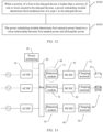
- FIG. 1 and FIG. 2 a structure of a charging pile system 100 in the embodiments and connection relationships and functions of modules of the charging pile system 100 are described by using FIG. 1 and FIG. 2 .
- FIG. 1 is a schematic structural diagram of a charging pile system 100 in an implementation according to an embodiment of this application.
- the charging pile system 100 includes at least one alternating current/direct current (Alternating Current/Direct Current, AC/DC) module 10, a bus module 20, a power scheduling module 30, a plurality of direct current/direct current (Direct Current/Direct Current, DC/DC) modules 40, and a plurality of charging terminals 50 that are connected to the plurality of DC/DC modules 40 in a one-to-one correspondence. It may be understood that there may be one or more AC/DC modules 10.
- FIG. 1 only shows a plurality of AC/DC modules 10.
- the charging pile system 100 may be applied to charging of another electronic device such as an electric vehicle, a mobile phone, or an ipad. This application sets no specific limitation.
- a to-be-charged device 60 in FIG. 1 in this embodiment is described by using an electric vehicle as an example.
- the AC/DC module 10 is configured to convert an alternating current of a power supply into a direct current.
- the AC/DC module 10 is configured to convert a high-voltage alternating current into a high-voltage direct current.
- a voltage of the high-voltage direct current is in a range of 500 volts to 1500 volts.
- a cable diameter of a conducting wire connected between the AC/DC module 10 and the bus module 20 is relatively small, and costs are also relatively low.
- the bus module 20 is configured to combine high-voltage direct currents converted by all AC/DC modules 10, and is configured to distribute a combined high-voltage direct current to each DC/DC module 40. Output ends of a plurality of AC/DC modules 10 are connected to input ends of the plurality of DC/DC modules 40 by using the bus module 20.
- the bus module 20 may be but is not limited to a conducting wire.
- the bus module 20 may alternatively be a combiner box.
- the power scheduling module 30 is configured to: determine a signal transmitted by each AC/DC module 10 and a signal transmitted by each DC/DC module 40, and control output power on each DC/DC module 40.
- the power scheduling module 30 is connected to the bus module 20. It may be understood that the power scheduling module 30 may be used as an independent part, or may be integrated into one or more modules in the plurality of AC/DC modules 10, the bus module 20, and the plurality of DC/DC modules 40. In other words, the power scheduling module 30 is a component in one or more modules in the plurality of AC/DC modules 10, the bus module 20, and the plurality of DC/DC modules 40.
- FIG. 2 is a schematic structural diagram of a charging pile system 100 in another implementation according to an embodiment of this application.
- the power scheduling module 30 is integrated into the bus module 20.
- the power scheduling module 30 is communicatively connected to all AC/DC modules 10 and all DC/DC modules 40. It may be understood that the power scheduling module 30 may be connected to all the AC/DC modules 10 and all the DC/DC modules 40 by using a radio signal, or may be connected to all the AC/DC modules 10 and all the DC/DC modules 40 in a wired manner.
- the power scheduling module 30 may alternatively be used as an independent part.
- the power scheduling module 30 is communicatively connected to all the AC/DC modules 10 and all the DC/DC modules 40.
- the power scheduling module 30 is integrated into the AC/DC module 10. It may be understood that when there is one AC/DC module 10, the power scheduling module 30 is integrated into the AC/DC module 10.
- the power scheduling module 30 is communicatively connected to all the DC/DC modules 40.
- the power scheduling module 30 may be integrated into one AC/DC module 10, or may be integrated into two or more AC/DC modules 10.
- the power scheduling module 30 is communicatively connected to another AC/DC module 10 and all the DC/DC modules 40.
- the power scheduling module 30 is communicatively connected to another DC/DC module 40 and all AC/DC modules 10.
- the power scheduling module 30 may be communicatively connected to another DC/DC module 40 and all the AC/DC modules 10.
- the DC/DC module 40 is configured to convert a direct current into a direct current.
- the DC/DC module 40 is configured to convert a high-voltage direct current into a low-voltage direct current.
- a voltage of the low-voltage direct current is in a range of 300 volts to 400 volts.
- a voltage range of the low-voltage direct current can meet a voltage requirement of a to-be-charged device.
- the to-be-charged device is an electric vehicle.
- the charging terminal 50 is configured to charge a to-be-charged device 60 based on transmit power determined by the corresponding DC/DC module 40. In other words, when the DC/DC module 40 determines transmit power transmitted by the power scheduling module 30, the DC/DC module 40 charges the to-be-charged device 60 by using the charging terminal 50.
- the charging terminal 50 is a connection end for charging the to-be-charged device 60.
- the to-be-charged device 60 when a to-be-charged device 60 is connected to the charging terminal 50, the to-be-charged device 60 has not entered a charging state.
- the to-be-charged device 60 is defined as a first to-be-charged device 61
- the charging terminal 50 connected to the first to-be-charged device 61 is a first charging terminal 51
- a DC/DC module 40 connected to the first charging terminal 51 is a first DC/DC module 41.
- a to-be-charged device 60 in the charging state is defined as a second to-be-charged device 62.
- a charging terminal 50 connected to the second to-be-charged device 62 is a second charging terminal 52.
- a DC/DC module 40 connected to the second charging terminal 52 is a second DC/DC module 42.
- the power scheduling module 30 can accurately control a value of output power of the first DC/DC module 41, to avoid a case in which another to-be-charged device 60 cannot be charged because too much power is allocated, and also to avoid a case in which a charging requirement of the to-be-charged device 60 cannot be met because too little power is allocated, so that utilization of the charging pile system 100 is improved.
- FIG. 3 is a schematic flowchart of an implementation of a method for managing the charging pile system 100 shown in FIG. 1 .
- FIG. 4 is a schematic diagram of a signal transmission path in the method for managing the charging pile system 100 shown in FIG. 3 .
- FIG. 5 is a schematic diagram of a current transmission path in the method for managing the charging pile system shown in FIG. 3 .
- FIG. 5 is only a schematic diagram of a current transmission path when the first to-be-charged device 61 is being charged.
- the method for managing the charging pile system 100 is described with reference to FIG. 3 to FIG. 5 .
- the method is performed by the power scheduling module 30 in FIG. 1 .
- the method includes but is not limited to S100, S200, and S300.
- a ranking of S100 and a ranking of S200 may alternatively be exchanged. This application sets no specific limitation.
- the power scheduling module 30 determines first needed power P nee/1 transmitted by the first DC/DC module 41 that is correspondingly connected to the first charging terminal 51.
- the first to-be-charged device 61 has a charging port, and the first charging terminal 51 may be connected to the charging port by using a charging wire.
- the first to-be-charged device 61 may be charged by using the charging port, and may also transmit a communication signal through the charging port.
- the power scheduling module 30 receives an electrical signal transmitted by the first to-be-charged device 61, and determines that the electrical signal is the first needed power P nee/1 .
- the first to-be-charged device 61 may alternatively be communicatively connected to the first DC/DC module 41 by using a radio signal.
- the power scheduling module 30 determines total surplus power P AC/DC/TSur transmitted by all AC/DC modules 10.
- the power scheduling module 30 determines, based on electrical signals transmitted by all the AC/DC modules 10, that the total surplus power P AC/DC/TSur is 2 kilowatts.
- the power scheduling module 30 receives an electrical signal transmitted by each AC/DC module 10, and determines surplus power of each AC/DC module 10 from the electrical signal.
- the power scheduling module 30 determines the total surplus power P AC/DC/TSur of all the AC/DC modules 10 based on the surplus power of each AC/DC module 10.
- transmitted power of the AC/DC module 10 is 0.
- transmitted power is calculated based on a product of a value of a transmitted voltage and a value of a transmitted current.
- the power scheduling module 30 transmits first transmit power P tra/1 to the first DC/DC module 41 based on a value relationship between the first needed power P nee/1 and the total surplus power P AC/DC/TSur . It may be understood that the power scheduling module 30 transmits an electrical signal to the first DC/DC module 41, so that the first DC/DC module 41 determines the first transmit power P tra/1 from the electrical signal. As shown in FIG. 5 , when the first DC/DC module 41 receives the first transmit power P tra/1 , the AC/DC module 10 starts to charge the first to-be-charged device 61. FIG. 5 shows output currents of all the AC/DC modules 10 to the first DC/DC module 41. In another implementation, currents may alternatively be output to the first DC/DC module 41 by using some AC/DC modules 10. Specifically, this is flexibly set based on a condition.
- the power scheduling module 30 when the power scheduling module 30 transmits the first transmit power P tra/1 to the first DC/DC module 41 by using S100, S200, and S300, the first DC/DC module 41 charges the first to-be-charged device 61 based on the first transmit power P tra/1 . In this case, the first to-be-charged device 61 obtains charging power whose value is the first transmit power P tra/1 . It may be understood that, because the power scheduling module 30 can transmit the first transmit power P tra/1 based on the value relationship between the first needed power P nee/1 and the total surplus power P AC/DC/TSur , a granularity of allocated power of the charging pile system 100 is relatively small.
- the power scheduling module 30 may control the DC/DC module to output any power such as 11 kilowatts, 13 kilowatts, or 33 kilowatts, and may even be accurate to a decimal point, for example, 11.1 kilowatts.
- a manner of combining closing and disconnection of a plurality of switch components is used, so that a plurality of charging modules are connected in parallel and then configured for one charging terminal.
- a granularity of allocated power of the charging pile system is relatively large.
- rated power of the AC/DC module 10 is 10 kilowatts.
- a power requirement that can be obtained by the to-be-charged device is power of a multiple of 10, such as 10 kilowatts, 20 kilowatts, or 30 kilowatts.
- the power scheduling module 30 can accurately control a value of output power of the first DC/DC module 41, to avoid a case in which another to-be-charged device 60 cannot be charged because too much power is allocated, and also to avoid a case in which a charging requirement of the to-be-charged device 60 cannot be met because too little power is allocated, so that utilization of the charging pile system 100 is improved.
- the conventional charging pile system significantly increases investment costs, and also significantly improves structural complexity of a charging pile.
- the newly added charging terminal 50 needs to be connected to the DC/DC module 40, and the DC/DC module 40 is communicatively connected to the power scheduling module 30. Therefore, the charging pile system 100 in this embodiment eliminates disposing of the plurality of switch components, and is relatively low in costs investment and is relatively simple in structure.
- the first transmit power P tra/1 is transmitted to the first DC/DC module 41 by using the power scheduling module 30, and the first transmit power P tra/1 is close to the first needed power P nee/1 .
- the DC/DC module 40 can accurately provide needed power for the first to-be-charged device 61, to better meet a charging requirement of the first to-be-charged device 61.
- the power scheduling module 30 transmits the first transmit power P tra/1 to the first DC/DC module 41.
- a ratio of the first transmit power P tra/1 to the first needed power P nee/1 falls within a preset range.
- the preset range is a value range [a, b] that is prestored on the power scheduling module 30.
- [0.9, 1.1] is all values from 0.9 to 1.1.
- the power scheduling module 30 may directly invoke the preset range.
- the power scheduling module 30 can transmit the first transmit power P tra/1 to the first DC/DC module 41, and the first transmit power P tra/1 is close to the first needed power P nee/1 , to control the first DC/DC module 41 to output the first transmit power P tra/1 that meets the charging requirement of the first to-be-charged device 61.
- the first to-be-charged device 61 can obtain charging power whose value is the first needed power P nee/1 . Therefore, power that can be obtained by the first to-be-charged device 61 is close to needed power of the first to-be-charged device 61, so that usability of the charging pile system 100 can be significantly improved.
- the power scheduling module 30 transmits the first transmit power P tra/1 to the first DC/DC module 41 by using the following several policy implementations, to allocate power to the first to-be-charged device 61.
- first come first served.
- the surplus power of all the AC/DC modules is transmitted to the first to-be-charged device 61, to better meet the charging requirement of the first to-be-charged device 61.
- some technical content that is of the method for managing the charging pile system 100 in this embodiment and that is the same as the method for managing the charging pile system 100 in the foregoing embodiment is not described again.
- a ratio of the first transmit power P tra/1 to the total surplus power P AC/DC/TSur falls within a preset range.
- the power scheduling module 30 controls the DC/DC module 40 to output the total surplus power P AC/DC/TSur to the first to-be-charged device 61.
- the total surplus power P AC/DC/TSur is closer to the charging requirement of the first to-be-charged device 61. This improves user experience of the charging pile system 100.
- power is equally allocated in proportion.
- the power scheduling module 30 allocates the total rated power P Trat to the first to-be-charged device 61 and the second to-be-charged device 62 in proportion, so that both the first to-be-charged device 61 and the second to-be-charged device 62 can obtain a part of needed power, to equitably allocate power to each to-be-charged device 60.
- FIG. 6 is a partial schematic flowchart of an implementation of a method for managing the charging pile system shown in FIG. 3 .
- FIG. 7 is a schematic diagram of a signal transmission path in the method for managing the charging pile system 100 shown in FIG. 6 .
- the method for managing the charging pile system 100 further includes but is not limited to S400 and S410.
- S400 and S410 may be exchanged.
- S400 and S410 are optional steps after S100, S200, and S300. To avoid excessive repetition, FIG. 6 provides only S400 and S410.
- some technical content that is of the method for managing the charging pile system 100 in this embodiment and that is the same as the method for managing the charging pile system 100 in the foregoing embodiment is not described again. Specific descriptions of S400 and S410 are as follows:
- the power scheduling module 30 determines second needed power P nee/2 transmitted by all second DC/DC modules 42 in the plurality of DC/DC modules 40.
- the power scheduling module 30 receives electrical signals transmitted by all the second DC/DC modules 42 in the plurality of DC/DC modules 40, and determines the second needed power P nee/2 from the electrical signals.
- the second DC/DC module 42 determines the second needed power P nee/2 in a plurality of manners.
- the second DC/DC module 42 determines a second needed voltage and a second needed current from the electrical signal.
- the second DC/DC module 42 calculates the second needed power P nee/2 based on the second needed voltage and the second needed current.
- the power scheduling module 30 receives the second needed power P nee/2 transmitted by the second DC/DC module 42.
- the second DC/DC module 42 receives an electrical signal of the second to-be-charged device 62 through the second charging terminal 52, and directly determines the second needed power P nee/2 from the electrical signal.
- the power scheduling module 30 determines second needed power P nee/2 includes: the power scheduling module 30 presets a transmission period in which the second DC/DC module 42 transmits the second needed power P nee/2 .
- the period is 10 minutes.
- the power scheduling module 30 determines, based on the transmission period, the second needed power P nee/2 transmitted by the second DC/DC module 42. For example, the power scheduling module 30 determines, once every 10 minutes, the second needed power P nee/2 transmitted by the second DC/DC module 42. Therefore, the second needed power P nee/2 determined by the power scheduling module 30 is closer to power actually needed by the second to-be-charged device 62, to avoid a case in which power allocated by the AC/DC module 10 is greater than the power actually needed by the second to-be-charged device 62, so that the charging pile system 100 can accurately provide a power requirement for the second to-be-charged device 62.
- the power scheduling module 30 determines total rated power P Trat transmitted by all AC/DC modules 10.
- the power scheduling module 30 receives an electrical signal transmitted by each AC/DC module 10, and determines rated power of each AC/DC module 10 from the electrical signal.
- the power scheduling module 30 determines the total rated power P Trat of all the AC/DC modules 10 based on the rated power of each AC/DC module 10.
- the power scheduling module 30 calculates the total rated power P Trat based on a sum of all the determined rated power, and calculates the total needed power P Tnee based on a sum of the determined second needed power P nee/2 and the determined first needed power P nee/1 .
- the power scheduling module 30 calculates an output power ratio k 1 based on the calculated total rated power P Trat and the calculated total needed power P Tnee .
- the power scheduling module 30 calculates the first output power P put/1 based on the output power ratio k 1 .
- the power scheduling module 30 controls the first DC/DC module 41 to output the first output power P put/1 to the first to-be-charged device 61, so that the first to-be-charged device 61 starts to be charged.
- the total rated power P Trat is allocated to the first to-be-charged device 61 and the second to-be-charged device 62 in proportion. Therefore, the first output power P put/1 received by the first to-be-charged device 61 is not equal to 0, to ensure that the first to-be-charged device 61 can be "immediately charged after arriving".
- the first DC/DC module 41 can charge the first to-be-charged device 61 by using the first charging terminal 51, to avoid a case in which a user gives up charging the first to-be-charged device 61 because the user needs to wait for excessively long charging time and consequently a user quantity of the charging pile system 100 is reduced.
- the power scheduling module 30 allocates the total rated power P Trat to the first to-be-charged device 61 in proportion, the first to-be-charged device 61 can obtain the first output power P put/1 in a relatively equitable manner.
- the output power ratio k 1 is 0.5. It is assumed that first needed power P nee/1 of the first to-be-charged device 61 is 20 kilowatts. In this case, power allocated to the first to-be-charged device 61 is 10 kilowatts. It may be understood that this allocation manner is relatively equitable, to be specific, when the total rated power P Trat is not enough to be allocated, specific power can also be allocated to the first to-be-charged device 61, to be used for charging.
- the total rated power P Trat is allocated to the first to-be-charged device 61 in proportion in the foregoing embodiment, the total rated power P Trat still has some surplus power.
- the surplus power is allocated to the second to-be-charged device 62 in the following S420, so that the second to-be-charged device 62 can obtain third transmit power P tra/3 in a relatively equitable manner.
- FIG. 8 is a partial schematic flowchart of another implementation of a method for managing the charging pile system shown in FIG. 3 .
- FIG. 9 is a schematic diagram of a signal transmission path in the method for managing the charging pile system 100 shown in FIG. 8 .
- the method for managing the charging pile system 100 further includes but is not limited to S420.
- S420 is an optional step after S400 and S410. To avoid excessive repetition, FIG. 8 provides only S420.
- S420 is an optional step after S400 and S410. To avoid excessive repetition, FIG. 8 provides only S420.
- S420 is an optional step after S400 and S410.
- FIG. 8 provides only S420.
- some technical content that is of the method for managing the charging pile system 100 in this embodiment and that is the same as the method for managing the charging pile system 100 in the foregoing embodiment is not described again. Specific descriptions of S420 are as follows:
- the power scheduling module 30 transmits third transmit power P tra/3 to the second DC/DC module 42, so that the second DC/DC module 42 charges the second to-be-charged device 62 based on the third transmit power P tra/3 by using the second charging terminal 52.
- the power scheduling module 30 calculates the third transmit power P tra/3 based on an output power ratio k 1 .
- the power scheduling module 30 transmits the third transmit power P tra/3 to the second DC/DC module 42, to control the second DC/DC module 42 to output the third transmit power P tra/3 that meets a charging requirement of the second to-be-charged device 62.
- the second to-be-charged device 62 can obtain charging power whose value is the third transmit power P tra/3 . Therefore, the first to-be-charged device 61 can obtain more accurate needed power, so that usability of the charging pile system 100 can be significantly improved.
- the power scheduling module 30 allocates the total rated power P Trat to the second to-be-charged device 62 in proportion, the second to-be-charged device 62 can obtain the third transmit power P tra/3 in a relatively equitable manner.
- the output power ratio k 1 is 0.5.
- second needed power P nee/2 of one second to-be-charged device 62 is 4 kilowatts.
- power allocated to the second to-be-charged device 62 is 2 kilowatts. It may be understood that this allocation manner is relatively equitable, to be specific, when the total rated power P Trat is not enough to be allocated, specific power can also be allocated to the second to-be-charged device 62, to be used for charging.
- power is allocated based on priorities.
- the power scheduling module 30 transmits the first transmit power P tra/1 to the first DC/DC module based on a relationship between a priority of the first to-be-charged device 61 and a priority of the second to-be-charged device 62, to better meet a charging requirement of a to-be-charged device 60 of a higher priority.
- FIG. 10 is a partial schematic flowchart of still another implementation of a method for managing the charging pile system shown in FIG. 3 .
- FIG. 11 is a schematic diagram of a signal transmission path in the method for managing the charging pile system 100 shown in FIG. 10 .
- the method for managing the charging pile system 100 further includes but is not limited to S500 and S510.
- S500 and S510 are optional steps after S100, S200, and S300.
- FIG. 10 provides only S500 and S510.
- some technical content that is of the method for managing the charging pile system 100 in this embodiment and that is the same as the methods for managing the charging pile system 100 in all the foregoing embodiments is not described again. Specific descriptions of S500 and S510 are as follows:
- the power scheduling module 30 receives identification information sent by the first to-be-charged device 61.
- the identification information may include but is not limited to a license plate number, an identity card number of a user, or a name of the user, and may even be a recognizable photo of the user.
- the power scheduling module 30 invokes a prestored priority database, and determines the priority of the first to-be-charged device 61 from the priority database based on the identification information.
- a priority of a to-be-charged device 60 has different levels in different time periods. For example, in an earlier period in which the charging pile system 100 is just put into use, priorities of different to-be-charged devices 60 may be distinguished based on a quantity of use times, to be specific, a higher quantity of use times leads to a higher priority. In this case, when the priorities of different to-be-charged devices 60 are distinguished based on the quantity of use times, the user can be effectively motivated to charge the to-be-charged devices 60 by using the charging pile system 100, to increase a quantity of charging times, thereby effectively popularizing use of the charging pile system 100 to increase a quantity of to-be-charged devices 60 that use the charging pile system 100.
- the priorities of different to-be-charged devices 60 may be distinguished based on an investment contribution of the charging pile system 100 or a credit score during use. Certainly, in another embodiment, the priority may alternatively be set in another manner. This application sets no specific limitation.
- the power scheduling module 30 determines the first transmit power P tra/1 based on a value relationship between the priority of the first to-be-charged device 61 and a priority of the second to-be-charged device 62.
- a to-be-charged device 60 of a higher priority can be preferentially charged, to better meet a charging requirement of the to-be-charged device 60 of the higher priority.
- FIG. 12 is a partial schematic flowchart of still another implementation of a method for managing the charging pile system shown in FIG. 3 .
- the method for managing the charging pile system 100 further includes but is not limited to S520 and S530.
- S520 and S530 are optional steps in S500 and S510.
- FIG. 11 provides only S520 and S530.
- S520 and S530 are as follows:
- the method may further include the following:
- the power scheduling module 30 determines priorities of all second to-be-charged devices 62. Specifically, the power scheduling module 30 invokes a prestored priority database, and determines the priorities of the second to-be-charged devices 62 from the priority database based on identification information of the second to-be-charged devices 62.
- the power scheduling module 30 sorts the priorities of the first to-be-charged device 61 and all the second to-be-charged devices 62. For example, the first to-be-charged device 61 or the second to-be-charged device 62 of a high priority is ranked first. A to-be-charged device of a low priority is deduced by analogy.
- the method may alternatively further include the following:
- the power scheduling module 30 invokes a ranking sequence of the priorities of all the second to-be-charged devices 62. Specifically, when each second to-be-charged device 62 is connected to the second charging terminal 52, the power scheduling module 30 immediately sorts, based on a prestored priority database, a priority of a newly connected second to-be-charged device 62 and a priority of a second to-be-charged device 62 that is being charged, to form the sorting sequence. In this case, when the first to-be-charged device 61 is connected to the first charging terminal 51, the power scheduling module 30 needs to invoke only the sorting sequence of the priorities of the second to-be-charged devices 62.
- the power scheduling module 30 determines a position of the priority of the first to-be-charged device 61 in the sorting sequence of the priorities of the second to-be-charged devices 62.
- the power scheduling module 30 places the priority of the first to-be-charged device 61 in the sorting sequence of the priorities of the second to-be-charged devices 62 through "bubble sort". For example, the priority of the first to-be-charged device 61 is first compared with a lowest level in the sorting sequence. When the priority of the first to-be-charged device 61 is higher than the lowest level, the priority of the first to-be-charged device 61 is then compared with a second lowest level in the sorting sequence. When the priority of the first to-be-charged device 61 is lower than the second lowest level, the priority of the first to-be-charged device 61 is placed between the lowest level and the second lowest level.
- the power scheduling module 30 presets a transmission period in which the third needed power P nee/3 is transmitted to the type-1 to-be-charged device 621.
- the transmission period is 10 minutes.
- the power scheduling module 30 determines, based on the transmission period, the third needed power P nee/3 transmitted by the second DC/DC module 42. For example, the power scheduling module 30 determines, once every 10 minutes, the third needed power P nee/3 transmitted by the second DC/DC module 42. It may be understood that the third needed power P nee/3 changes after the type-1 to-be-charged device 621 has been charged for a period of time. Therefore, the third needed power P nee/3 transmitted by the second DC/DC module 42 is determined once every 10 minutes by using the power scheduling module 30, so that the third needed power P nee/3 determined by the power scheduling module 30 is closer to power actually needed by the type-1 to-be-charged device 621. In other words, power allocated by the AC/DC module 10 to the type-1 to-be-charged device 621 is avoided from being greater than the actually needed power.
- the power scheduling module 30 determines the first transmit power P tra/1 based on a value relationship between the first needed power P nee/1 and allocatable power P allo .
- the priority of the first to-be-charged device 61 is higher than a priority of one or more second to-be-charged devices 62, a charging requirement of the first to-be-charged device 61 of a higher priority is better met based on the value relationship between the first needed power P nee/1 and the allocatable power P allo .
- a ratio of the first transmit power P tra/1 to the allocatable power P allo falls within a preset range.
- the power scheduling module 30 calculates the allocatable power P allo based on a sum of the total surplus power P AC/DC/TSur and third needed power P nee/3 of all type-1 to-be-charged devices 621.
- the allocatable power P allo cannot meet or exactly meets the charging requirement of the first to-be-charged device 61.
- the first transmit power P tra/1 transmitted to the first DC/DC module 41 by using the power scheduling module 30 is close to the allocatable power P allo , so that the charging requirement of the first to-be-charged device 61 can be better met. This ensures that charging of the first to-be-charged device 61 can be more quickly completed.
- the first transmit power P tra/1 cannot be equal to 0.
- the first to-be-charged device 61 can be "immediately charged after arriving".
- the first DC/DC module 41 can charge the first to-be-charged device 61 by using the first charging terminal 51, to avoid a case in which a user gives up charging the first to-be-charged device 61 because the user needs to wait for excessively long charging time and consequently a user quantity of the charging pile system 100 is reduced.
- the third needed power P nee/3 allocated to all the type-1 to-be-charged devices 621 is reallocated to the first to-be-charged device 61 of a higher priority, to better meet the charging requirement of the first to-be-charged device 61 of the higher priority. This facilitates development of a to-be-charged device 60 of a relatively low priority toward a higher priority.
- the first transmit power P tra/1 obtained by the first to-be-charged device 61 is close to the allocatable power P allo . Therefore, a part of power obtained by the first to-be-charged device 61 comes from power that has been allocated to the type-1 to-be-charged device 621.
- the power scheduling module 30 controls the second DC/DC module 42 to transmit fourth transmit power P tra/4 to the type-1 to-be-charged device 621.
- the power scheduling module 30 transmits the fourth transmit power P tra/4 to a second DC/DC module 42 corresponding to the type-1 to-be-charged device 621.
- the fourth transmit power P tra/4 is equal to 0. It may be understood that because the fourth transmit power P tra/4 is equal to 0, the second charging terminal 52 stops charging the type-1 to-be-charged device 621. In this case, by using the foregoing method, the type-1 to-be-charged device 621 can develop towards a higher priority.
- the power scheduling module 30 transmits the first transmit power P tra/1 to the first DC/DC module 41 when the first needed power P nee/1 is greater than or equal to the allocatable power P allo is provided above. That the power scheduling module 30 transmits the first transmit power P tra/1 to the first DC/DC module 41 by using the following policy when the first needed power P nee/1 is less than the allocatable power P allo is provided below.
- the first DC/DC module 41 charges the first to-be-charged device 61 based on the first transmit power P tra/1 by using the first charging terminal 51, so that the first to-be-charged device 61 starts to be charged.
- the allocatable power P allo can meet the charging requirement of the first to-be-charged device 61.
- the first transmit power P tra/1 transmitted by using the power scheduling module 30 is close to the first needed power P nee/1 .
- the first DC/DC module 41 can accurately provide needed power for the first to-be-charged device 61, to better meet the charging requirement of the first to-be-charged device 61.
- second transmit power P tra/2 obtained by the first to-be-charged device 61 is close to the first needed power P nee/1 , and the first needed power P nee/1 is less than the allocatable power P all . Therefore, a part of power obtained by the first to-be-charged device 61 comes from power that has been allocated to the type-1 to-be-charged device 621. In this case, power is allocated to the type-1 to-be-charged device 621 by using the following method.
- the power scheduling module 30 can reallocate a part of the allocatable power P allo to a type-1 to-be-charged device 621 of a higher priority, so that a charging requirement of the type-1 to-be-charged device 621 of the higher priority is met to a relatively large extent.
- the power scheduling module 30 transmits first output power P put/1 to a second DC/DC module 42 corresponding to a type-1 to-be-charged device 621 whose priority is i, so that the second DC/DC module 42 charges, based on the first output power P put/1 by using the second charging terminal 52, the type-1 to-be-charged device 621 whose priority is i.
- a ratio of the first output power P put/1 to the i th surplus power P Sur/i falls within a preset range.
- the first needed power P nee/1 is less than the i th power P i
- the allocatable power P allo is equal to the sum of the total surplus power P AC/DC/TSur and third needed power P nee/3 of all type-1 to-be-charged devices 621
- the first needed power P nee/1 is also obviously less than the allocatable power P allo .
- the power scheduling module 30 transmits fifth transmit power P tra/5 to second DC/DC modules 42 corresponding to all type-1 to-be-charged devices 621 whose priorities are lower than i, and the fifth transmit power P tra/5 is 0.
- the i th surplus power P Sur/i is equal to a difference between the i th power P i and the first needed power P nee/1 .
- a quantity of type-1 to-be-charged devices is 3, and i is equal to 2.
- second power P 2 is equal to a sum of the total surplus power P AC/DC/TSur , third needed power P nee/3 of a type-1 to-be-charged device 621 whose priority is 3, and third needed power P nee/3 of a type-1 to-be-charged device 621 whose priority is 2.
- Third power P 3 is equal to a sum of the total surplus power P AC/DC/TSur and the third needed power P nee/3 of the type-1 to-be-charged device 621 whose priority is 3.
- the power scheduling module 30 transmits the first output power P put/1 to a second DC/DC module 42 corresponding to the type-1 to-be-charged device 621 whose priority is 2, so that the second DC/DC module 42 charges, based on the first output power P put/1 by using the second charging terminal 52, the type-1 to-be-charged device 621 whose priority is 2.
- the power scheduling module 30 stops charging the to-be-charged device 621 whose priority is 3.
- the third needed power P nee/3 that has been allocated to the type-1 to-be-charged device 621 whose priority is 3 is reallocated to the first to-be-charged device 61.
- first needed power P nee/1 is less than or equal to the second power P 2
- a part of third needed power P nee/3 that has been allocated to the type-1 to-be-charged device 621 whose priority is 2 is reallocated to the first to-be-charged device 61, to meet the charging requirement of the first to-be-charged device 61 to a relatively large extent.
- the power scheduling module 30 calculates the i th power P; based on a sum of the total surplus power P AC/DC/TSur and third needed power P nee/3 of all type-1 to-be-charged devices 621 whose priorities are lower than or equal to i.
- the power scheduling module 30 calculates the (i+1) th power P i+1 based on a sum of the total surplus power P AC/DC/TSur and third needed power P nee/3 of all type-1 to-be-charged devices whose priorities are lower than or equal to i+1.
- the power scheduling module 30 calculates the i th surplus power P Sur/i based on a difference between the i th power P i and the first needed power P nee/1 .
- the power scheduling module 30 reallocates, to the first to-be-charged device 61 of a higher priority, a part of power allocated to the type-1 to-be-charged device 621, the power allocated to the type-1 to-be-charged device 621 still has another surplus part.
- the power scheduling module 30 allocates the another surplus part of power to a second to-be-charged device 62 of a highest priority in the type-1 to-be-charged device 621, so that charging of a type-1 to-be-charged device 621 of a higher priority can be quickly completed, to meet a charging requirement of a to-be-charged device 60 of a higher priority to a relatively large extent.
- All the foregoing allocation manners are power allocation manners for transmitting power to the first DC/DC module 41 when the priority of the first to-be-charged device 61 is higher than the priority of the one or more second to-be-charged devices 62.
- a power allocation manner used when the priority of the first to-be-charged device 61 is lower than or equal to a priority of any second to-be-charged device 62 is provided below.
- the priority of the first to-be-charged device 61 when the priority of the first to-be-charged device 61 is lower than or equal to the priority of any second to-be-charged device 62, power transmitted by the power scheduling module 30 to the first DC/DC module 41 is 0. In this case, the first DC/DC module 41 does not charge the first to-be-charged device 61. Therefore, in this method, the first to-be-charged device 61 of a relatively low priority can be motivated to develop towards to a higher priority.
- power is allocated equally in proportion based on priorities.
- the allocatable power P allo is allocated to the first to-be-charged device 61 and the type-1 to-be-charged device 621 based on an output power ratio, so that power can be allocated to both the first to-be-charged device 61 and the type-1 to-be-charged device 621, thereby ensuring equitable power allocation.
- this embodiment also includes steps such as S500, S510, S520, and S530. Different technical content is specifically described below in detail.
- the first DC/DC module 41 charges the first to-be-charged device 61 based on the first transmit power P tra/1 by using the first charging terminal 51.
- the first to-be-charged device 61 can be "immediately charged after arriving".
- the first DC/DC module 41 can charge the first to-be-charged device 61 by using the first charging terminal 51, to avoid a case in which a user gives up charging the first to-be-charged device 61 because the user needs to wait for excessively long charging time and consequently a user quantity of the charging pile system 100 is reduced.
- the priority of the first to-be-charged device 61 is higher than a priority of one or more second to-be-charged devices 62, the first to-be-charged device 61 of a higher priority can also be preferentially charged by using the foregoing method.
- the allocatable power P allo is allocated to the first to-be-charged device 61 based on the output power ratio k 2 , power allocated to the first to-be-charged device 61 is also relatively equitable. It may be understood that, when the allocatable power P allo is not enough to be allocated, specific power can also be allocated to the first to-be-charged device 61, to be used for charging.
- the allocatable power P allo is allocated to the first to-be-charged device 61 in proportion in the foregoing embodiment, the allocatable power P allo still has some surplus power.
- the surplus power is allocated to the type-1 to-be-charged device 621 by using the following method, so that the type-1 to-be-charged device 621 can obtain sixth transmit power in a relatively equitable manner.
- the power scheduling module 30 calculates the fourth output power P put/4 based on a product of the output power ratio k 2 and the third needed power P nee/3 .
- the allocatable power P allo is allocated to the first to-be-charged device 61 and the type-1 to-be-charged device 621 based on the output power ratio k 2 , to relatively equitably allocate power to the first to-be-charged device 61 and the type-1 to-be-charged device 621.
- a case in which use experience of the user is affected because some to-be-charged devices 60 are not charged and some to-be-charged devices 60 are being charged due to a power allocation imbalance.
- the priority of the first to-be-charged device 61 is higher than the priority of the one or more second to-be-charged devices 62, the first to-be-charged device 61 is connected to the charging terminal 50 later than the type-1 to-be-charged device 621. Therefore, the allocatable power P allo is allocated to the first to-be-charged device 61 and the type-1 to-be-charged device 621 based on the output power ratio k 2 , so that it is ensured that the first to-be-charged device 61 of the higher priority can be preferentially charged, and the type-1 to-be-charged device can also continue to be charged.
- All the foregoing allocation manners are power allocation manners in which the power scheduling module 30 allocates power to the first DC/DC module 41 when the priority of the first to-be-charged device 61 is higher than the priority of the one or more second to-be-charged devices 62.
- a power allocation manner used when the priority of the first to-be-charged device 61 is lower than or equal to a priority of any second to-be-charged device 62 is provided below.
- the charging pile system 100 may further include a detection module 70.
- the detection module 70 is configured to detect whether a circuit fault occurs between the bus module 20 and the DC/DC module 40, so that when one charging circuit is faulty, the faulty charging circuit does not affect another charging circuit.
- a structure of the charging pile system 100 in this embodiment and a function of the detection module 70 in the charging circuit are described by using FIG. 13 and FIG. 14 .
- FIG. 13 is a schematic structural diagram of a charging pile system 100 in still another implementation according to an embodiment of this application.
- the charging pile system 100 includes a plurality of detection modules 70.
- the plurality of detection modules 70 are connected between the bus module 20 and the plurality of DC/DC modules 40 in a one-to-one correspondence.
- the detection module 70 is configured to detect whether a circuit fault occurs between the bus module 20 and the DC/DC module 40.
- the power scheduling module 30 controls the detection module 70, so that the bus module 20 and the first DC/DC module 41 are in an open-circuit state.
- the detection module 70 connected between the bus module 20 and the first DC/DC module 41 is a first detection module 71.
- the first detection module 71 is configured to detect whether a circuit fault occurs between the bus module 20 and the first DC/DC module 41.
- a detection module 70 connected between the bus module 20 and the second DC/DC module 42 is a second detection module 72.
- the second detection module 72 is configured to detect whether a circuit fault occurs between the bus module 20 and the second DC/DC module 42.
- FIG. 14 is a schematic structural diagram of the detection module 70 in the charging pile system 100 shown in FIG. 13 .
- the detection module 70 includes a load current detection part 71, a leakage current detection part 72, and a controllable switch part 73.
- the load current detection part 71, the leakage current detection part 72, and the controllable switch part 73 are connected in series.
- the load current detection part 71 may also be connected in parallel to the leakage current detection part 72, and then connected in series to the controllable switch part 73. It may be understood that the load current detection part 71 is configured to detect whether a load current between the bus module 20 and the DC/DC module 40 is greater than or equal to a preset load current threshold.
- the leakage current detection part 72 is configured to detect whether a leakage current between the bus module 20 and the DC/DC module 40 is greater than or equal to a preset leakage current threshold.
- the controllable switch part 73 is configured to disconnect a connection between the bus module 20 and the DC/DC module 40.
- the detection module 70 further includes a fault isolation controller 74.
- the fault isolation controller 74 is communicatively connected to the power scheduling module 30.
- the fault isolation controller 74 is sequentially connected to the load current detection part 71, the leakage current detection part 72, and the controllable switch part 73.
- the fault isolation controller 74 may control detection of the load current detection part 71 and the leakage current detection part 72 based on a signal of the power scheduling module 30, and may further control closing and disconnection of the controllable switch part 73.
- the power scheduling module 30 may be integrated into the fault isolation controller 74.
- the charging circuit of the first to-be-charged device 61 does not affect a charging circuit of the second to-be-charged device 62.
- FIG. 15 is a schematic flowchart of a method for managing the charging pile system 100 shown in FIG. 13 .
- the method for managing the charging pile system 100 further includes but is not limited to S600.
- S600 may be an optional step after any step in the methods for managing the charging pile system in the foregoing embodiments. To avoid excessive repetition, FIG. 15 provides only S600.
- S600 some technical content that is of the method for managing the charging pile system 100 in this embodiment and that is the same as the method for managing the charging pile system 100 in the foregoing embodiment is not described again. Specific descriptions of S600 are as follows:
- the power scheduling module 30 controls the first detection module 71, so that the bus module 20 and the first DC/DC module 41 are in an open-circuit state.
- the power scheduling module 30 controls the first detection module 71, so that the bus module 20 and the first DC/DC module 41 are in an open-circuit state.
- the preset load current threshold is 50 amperes
- the preset leakage current threshold is 30 amperes.
- the power scheduling module 30 controls the first detection module 71, so that the bus module 20 and the first DC/DC module 41 are in an open-circuit state.
- the power detection module 70 prestores the preset load current threshold, or the power detection module 70 prestores the preset leakage current threshold.
- the load current threshold may be preset based on a bearing capacity of a conducting wire between the bus module 20 and the first DC/DC module 41.
- This application further provides a charging pile system corresponding to the methods for managing the charging pile system in the foregoing embodiments.
- the power scheduling module in the charging pile system is configured to perform the methods for managing the charging pile system in the foregoing embodiments.
Description
- This application relates to the field of electric vehicle charging technologies, and in particular, to a method for managing a charging pile system and a charging pile system.
- A charging pile system is used to convert electrical energy of a power grid into direct currents of different voltages and different currents, to directly charge a battery of an electric vehicle by using a charging connection apparatus. A conventional direct-current charging pile system includes an input bus, a plurality of charging modules, a plurality of switch components, and a plurality of charging terminals. The input bus is configured to connect an input power supply to the plurality of charging modules. The charging module is configured to convert electrical energy of the input bus into a direct current of a specification needed by the electric vehicle. In addition, in a manner of combining closing and disconnection of the plurality of switch components, the plurality of charging modules are configured in parallel and then configured for one charging terminal, to charge the battery of the electric vehicle by using the charging terminal. However, power configured by the plurality of charging modules connected in parallel for the electric vehicle cannot accurately meet needed power of the electric vehicle, and consequently usability of the charging pile system is poor.
CN107492941A refers to an airport ground power supply based charging pile device, has power supply input module fixedly connected with power supply module through bus, and control module controls power supply input module to charge charging pile module. -
CN105896690B refers to a mixed energy system for electric vehicle charging and monitoring device, has solar energy controller provided with multiple solar energy arrays, and DC-DC inverter controller whose output end is connected to direct current charging connector. - Embodiments of this application provide a method for managing a charging pile system and a charging pile system. By using the method for managing a charging pile system, the charging pile system can accurately meet a charging requirement of a to-be-charged device. These effects are achieved by the subject matter of the independent claims. Further implementation forms are provided in the dependent claims.
- According to a first aspect, an embodiment of this application provides a method for managing a charging pile system. The charging pile system includes at least one alternating current/direct current (Alternating Current/Direct Current, AC/DC) module, a bus module, a power scheduling module, a plurality of direct current/direct current (Direct Current/Direct Current, DC/DC) modules, and a plurality of charging terminals that are connected to the plurality of DC/DC modules in a one-to-one correspondence.
- The AC/DC module is configured to convert an alternating current of a power supply into a direct current. Optionally, the AC/DC module is configured to convert a high-voltage alternating current into a high-voltage direct current. A voltage of the high-voltage direct current is in a range of 500 volts to 1500 volts. In this case, a cable diameter of a conducting wire connected between the AC/DC module and the bus module is relatively small, and costs are also relatively low.
- The bus module is configured to combine high-voltage direct currents converted by all AC/DC modules, and is configured to distribute a combined high-voltage direct current to each DC/DC module. Output ends of a plurality of AC/DC modules are connected to input ends of the plurality of DC/DC modules by using the bus module. Optionally, the bus module may be but is not limited to a conducting wire. For example, the bus module may alternatively be a combiner box.
- The power scheduling module is configured to: determine a signal transmitted by each AC/DC module and a signal transmitted by each DC/DC module, and control output power on each DC/DC module. In addition, the power scheduling module is connected to the bus module. It may be understood that the power scheduling module may be used as an independent part, or may be integrated into one or more modules in the AC/DC module, the bus module, and the DC/DC module. In other words, the power scheduling module is a component in one or more modules in the plurality of AC/DC modules, the bus module, and the plurality of DC/DC modules.
- The DC/DC module is configured to convert a direct current into a direct current. Optionally, the DC/DC module is configured to convert a high-voltage direct current into a low-voltage direct current. A voltage of the low-voltage direct current is in a range of 300 volts to 400 volts. In this case, a voltage range of the low-voltage direct current can meet a voltage requirement of a to-be-charged device. For example, the to-be-charged device is an electric vehicle.
- The charging terminal is configured to charge the to-be-charged device based on transmit power determined by the corresponding DC/DC module. In other words, when the DC/DC module determines transmit power transmitted by the power scheduling module, the DC/DC module charges the to-be-charged device by using the charging terminal.
- In this application, when a to-be-charged device is connected to the charging terminal, the to-be-charged device has not entered a charging state. In this case, in this embodiment, the to-be-charged device is defined as a first to-be-charged device, a charging terminal connected to the to-be-charged device is a first charging terminal, and a DC/DC module connected to the first charging terminal is a first DC/DC module.
- In addition, a to-be-charged device in the charging state is defined as a second to-be-charged device. A charging terminal connected to the second to-be-charged device is a second charging terminal. A DC/DC module connected to the second charging terminal is a second DC/DC module.
- The method includes:
when the first charging terminal in the plurality of charging terminals is connected to the first to-be-charged device, the power scheduling module determines first needed power Pnee/1 transmitted by the first DC/DC module that is correspondingly connected to the first charging terminal. - It may be understood that the first to-be-charged device has a charging port, and the first charging terminal may be connected to the charging port by using a charging wire. The first to-be-charged device may be charged by using the charging port, and may also transmit a communication signal through the charging port. In this case, the power scheduling module receives an electrical signal transmitted by the first to-be-charged device, and determines that the electrical signal is the first needed power Pnee/1. In another implementation, when the first charging terminal is connected to the first to-be-charged device, the first to-be-charged device may alternatively be communicatively connected to the first DC/DC module by using a radio signal.
- The power scheduling module determines total surplus power transmitted by the at least one AC/DC modules.
- It may be understood that, when the AC/DC module does not transmit a current to the DC/DC module, transmitted power of the AC/DC module is 0. When the AC/DC module transmits a current to the DC/DC module, transmitted power is calculated based on a product of a value of a transmitted voltage and a value of a transmitted current.
- The power scheduling module transmits first transmit power Ptra/1 to the first DC/DC module based on a value relationship between the first needed power Pnee/1 and the total surplus power PAC/DC/TSur.
- In this embodiment, when the power scheduling module transmits the first transmit power Ptra/1 to the first DC/DC module, the first DC/DC module charges the first to-be-charged device based on the first transmit power Ptra/1. In this case, the first to-be-charged device obtains charging power whose value is the first transmit power Ptra/1. It may be understood that, because the power scheduling module can transmit the first transmit power Ptra/1 based on the value relationship between the first needed power Pnee/1 and the total surplus power PAC/DC/TSur, a granularity of allocated power of the charging pile system is relatively small.
- In an embodiment, when the first needed power Pnee/1 is less than or equal to the total surplus power PAC/DC/TSur, a ratio of the first transmit power Ptra/1 to the first needed power Pnee/1 falls within a preset range.
- It may be understood that, when the power scheduling module transmits the first transmit power Ptra/1 to the first DC/DC module, the first DC/DC module charges the first to-be-charged device based on the first transmit power Ptra/1. In this case, the first to-be-charged device obtains charging power whose value is the first needed power Pnee/1. In another implementation, currents may alternatively be output to the first DC/DC module by using some AC/DC modules. Specifically, this is flexibly set based on a condition.
- In addition, the preset range is a value range [a, b] that is prestored on the power scheduling module. Optionally, [0.9, 1.1] is all values from 0.9 to 1.1. When the power scheduling module needs to use the preset range, the power scheduling module may directly invoke the preset range.
- In this embodiment, in the foregoing method, when the first needed power Pnee/1 is less than or equal to the total surplus power PAC/DC/TSur, the power scheduling module can transmit the first transmit power Ptra/1 to the first DC/DC module, and the first transmit power Ptra/1 is close to the first needed power Pnee/1, to control the first DC/DC module to output the first transmit power Ptra/1 that meets a charging requirement of the first to-be-charged device. In this case, the first to-be-charged device can obtain charging power whose value is the first needed power Pnee/1. Therefore, power that can be obtained by the first to-be-charged device is close to needed power of the first to-be-charged device, so that usability of the charging pile system can be significantly improved.
- In an embodiment, when the first needed power Pnee/1 is greater than the total surplus power PAC/DC/TSur, a ratio of the first transmit power Ptra/1 to the total surplus power PAC/DC/TSur falls within a preset range.
- In this embodiment, when the first needed power Pnee/1 is greater than the total surplus power PAC/DC/TSur, the power scheduling module controls the DC/DC module to output the total surplus power PAC/DC/TSur to the first to-be-charged device. In this case, the total surplus power PAC/DC/TSur is closer to the charging requirement of the first to-be-charged device. This improves user experience of the
charging pile system 100. - In an embodiment, when the first needed power Pnee/1 is greater than the total surplus power PAC/DC/TSur, a ratio of the first transmit power Ptra/1 to first output power Pput/1 falls within a preset range, where Pput/1=k1×Pnee/1; and k1=PTrat/PTnee; where k1 is an output power ratio, PTrat is total rated power of all the AC/DC modules, PTnee is a sum of all second needed power Pnee/2 and the first needed power Pnee/1, and the second needed power Pnee/2 is needed power of a second to-be-charged device corresponding to the second DC/DC module, where a charging terminal connected to the second to-be-charged device in the charging state is the second charging terminal, and a DC/DC module corresponding to the second charging terminal in the plurality of charging terminals is the second DC/DC module; and
the method further includes:
the power scheduling module determines second needed power Pnee/2 transmitted by all second DC/DC modules in the plurality of DC/DC modules. - It may be understood that, the power scheduling module receives electrical signals transmitted by all the second DC/DC modules in the plurality of DC/DC modules, and determines the second needed power Pnee/2 from the electrical signals.
- The second DC/DC module determines the second needed power Pnee/2 in a plurality of manners.
- In an implementation, after the second DC/DC module receives an electrical signal of the second to-be-charged device through the second charging terminal, and determines a second needed voltage and a second needed current from the electrical signal, the second DC/DC module calculates the second needed power Pnee/2 based on the second needed voltage and the second needed current. The power scheduling module determines the second needed power Pnee/2 transmitted by the second DC/DC module.
- In another implementation, the second DC/DC module receives an electrical signal of the second to-be-charged device through the second charging terminal, and determines the second needed power Pnee/2 from the electrical signal.
- Optionally, that the power scheduling module determines the second needed power Pnee/2 includes:
the power scheduling module presets a transmission period in which the second DC/DC module transmits the second needed power Pnee/2. For example, the period is 10 minutes. - The power scheduling module determines, based on the transmission period, the second needed power Pnee/2 transmitted by the second DC/DC module. For example, the power scheduling module determines, once every 10 minutes, the second needed power Pnee/2 transmitted by the second DC/DC module. Therefore, the second needed power Pnee/2 determined by the power scheduling module is closer to power actually needed by the second to-be-charged device, to avoid a case in which power allocated by the AC/DC module is greater than the power actually needed by the second to-be-charged device, so that the charging pile system can accurately provide a power requirement for the second to-be-charged device.
- The power scheduling module determines total rated power transmitted by the at least one AC/DC modules. Optionally, the power scheduling module receives an electrical signal of rated power transmitted by each AC/DC module, and determines the rated power from the electrical signal. In this case, the power scheduling module determines the total rated power transmitted by the at least one AC/DC modules.
- Optionally, the power scheduling module calculates the total rated power PTrat based on a sum of all the determined rated power, and calculates the total needed power PTnee based on a sum of the determined second needed power Pnee/2 and the determined first needed power Pnee/1. In addition, the power scheduling module calculates the output power ratio k1 based on the calculated total rated power PTrat and the calculated total needed power PTnee. Finally, the power scheduling module calculates the first output power Pput/1 based on the output power ratio k1.
- In this embodiment, in the foregoing method, when the first needed power Pnee/1 is greater than the total surplus power PAC/DC/TSur, the power scheduling module controls the first DC/DC module to output the first output power Pput/1 to the first to-be-charged device, so that the first to-be-charged device starts to be charged.
- It may be understood that, in this implementation, the total rated power PTrat is allocated to the first to-be-charged device and the second to-be-charged device in proportion. Therefore, the first output power Pput/1 received by the first to-be-charged device is not equal to 0, to ensure that the first to-be-charged device can be "immediately charged after arriving". In other words, once the first to-be-charged device is connected to the first charging terminal, the first DC/DC module can charge the first to-be-charged device by using the first charging terminal, to avoid a case in which a user gives up charging the first to-be-charged device because the user needs to wait for excessively long charging time and consequently a user quantity of the charging pile system is reduced.
- In addition, because the power scheduling module allocates the total rated power PTrat to the first to-be-charged device in proportion, the first to-be-charged device can obtain the first transmit power Ptra/1 in a relatively equitable manner.
- In an embodiment, when the first needed power Pnee/1 is greater than the total surplus power PAC/DC/TSur, the power scheduling module transmits third transmit power Ptra/3 to the second DC/DC module, so that the second DC/DC module charges the second to-be-charged device based on the third transmit power Ptra/3 by using the second charging terminal. A ratio of the third transmit power Ptra/3 to second output power Pput/2 falls within a preset range, where
Pput/2=k1×Pnee/2.
- Optionally, the power scheduling module calculates the third transmit power Ptra/3 based on an output power ratio k1.
- In this embodiment, in the foregoing method, when the first needed power Pnee/1 is greater than the total surplus power PAC/DC/TSur, the power scheduling module transmits the third transmit power Ptra/3 to the second DC/DC module, to control the second DC/DC module to output the third transmit power Ptra/3 that meets a charging requirement of the second to-be-charged device. In this case, the second to-be-charged device can obtain charging power whose value is the third transmit power Ptra/3. Therefore, the first to-be-charged device can obtain more accurate needed power, so that usability of the charging pile system can be significantly improved.
- In addition, because the power scheduling module allocates the total rated power PTrat to the second to-be-charged device in proportion, the second to-be-charged device can obtain the third transmit power Ptra/3 in a relatively equitable manner.
- In an embodiment, when the first needed power Pnee/1 is greater than the total surplus power PAC/DC/TSur, the power scheduling module determines a priority of the first to-be-charged device.
- Optionally, when the first charging terminal in the plurality of charging terminals is connected to the first to-be-charged device, the power scheduling module receives identification information sent by the first to-be-charged device. The identification information may include but is not limited to a license plate number, an identity card number of the user, or a name of the user, and may even be a recognizable photo of the user.
- The power scheduling module invokes a prestored priority database, and determines the priority of the first to-be-charged device from the priority database based on the identification information.
- The power scheduling module determines the first transmit power Ptra/1 based on a relationship between the priority of the first to-be-charged device and a priority of the second to-be-charged device, where a DC/DC module corresponding to a second charging terminal in the plurality of charging terminals is a second DC/DC module, and a charging terminal connected to the second to-be-charged device in the charging state is the second charging terminal.
- In this implementation, in the foregoing method, a to-be-charged device of a higher priority can be preferentially charged, to better meet a charging requirement of the to-be-charged device of the higher priority.
- Further, the method further includes:
when the priority of the first to-be-charged device is higher than a priority of one or more second to-be-charged devices, the power scheduling module determines third needed power Pnee/3 of a type-1 to-be-charged device, where the type-1 to-be-charged device is a second to-be-charged device whose priority is lower than the priority of the first to-be-charged device. - Optionally, the power scheduling module presets a transmission period in which the third needed power Pnee/3 is transmitted to the type-1 to-be-charged device. For example, the transmission period is 10 minutes.
- The power scheduling module determines, based on the transmission period, the third needed power Pnee/3 transmitted by the second DC/DC module. Therefore, the third needed power Pnee/3 transmitted by the second DC/DC module is determined once every 10 minutes by using the power scheduling module, so that the third needed power Pnee/3 determined by the power scheduling module is closer to power actually needed by the type-1 to-
be-charged device 621. In other words, power allocated by the AC/DC module to the type-1 to-be-charged device is avoided from being greater than the actually needed power. - The power scheduling module determines the first transmit power Ptra/1 based on a value relationship between the first needed power Pnee/1 and allocatable power Pallo, and the allocatable power Pallo is equal to a sum of the total surplus power PAC/DC/TSur and third needed power Pnee/3 of all type-1 to-be-charged devices.
- In this embodiment, because the priority of the first to-be-charged device is higher than the priority of the one or more second to-be-charged devices, a charging requirement of the first to-be-charged device of a higher priority is better met by using the value relationship between the first needed power and the allocatable power.
- In an implementation, when the first needed power Pnee/1 is greater than or equal to the allocatable power Pallo, a ratio of the first transmit power Ptra/1 to the allocatable power Pallo falls within a preset range.
- In this implementation, because the first needed power Pnee/1 is greater than or equal to the allocatable power Pallo, the allocatable power Pallo cannot meet or exactly meets the charging requirement of the first to-be-charged device. In this case, the first transmit power Ptra/1 transmitted to the first DC/DC module by using the power scheduling module is close to the allocatable power Pallo, so that the charging requirement of the first to-be-charged device can be better met. This ensures that charging of the first to-be-charged device can be more quickly completed.
- The method further includes:
the power scheduling module transmits fourth transmit power Ptra/4 to a second DC/DC module corresponding to the type-1 to-be-charged device, where the fourth transmit power Ptra/4 is equal to 0. - It may be understood that, because the fourth transmit power Ptra/4 is equal to 0, the second charging terminal stops charging the type-1 to-be-charged device. In this case, in the foregoing method, the type-1 to-be-charged device can be motivated to develop towards a higher priority.
- In an embodiment, when the first needed power Pnee/1 is less than the allocatable power Pallo, a ratio of the first transmit power Ptra/1 to the first needed power Pnee/1 falls within a preset range.
- Because the first needed power Pnee/1 is less than the allocatable power Pallo, the allocatable power Pallo can meet the charging requirement of the first to-be-charged device. In this case, the first transmit power Ptra/1 transmitted by using the power scheduling module is close to the first needed power Pnee/1. In this case, the first DC/DC module can accurately provide needed power for the first to-be-charged device, to better meet the charging requirement of the first to-be-charged device.
- In an embodiment, when the first needed power Pnee/1 is greater than (i+1)th power Pi+1 and the first needed power Pnee/1 is less than or equal to ith power Pi, the power scheduling module transmits the first output power Pput/1 to a second DC/DC module corresponding to a type-1 to-be-charged device whose priority is i, so that the second DC/DC module charges, based on the first output power Pput/1 by using the second charging terminal, the type-1 to-be-charged device whose priority is i. A ratio of the first output power Pput/1 to ith surplus power PSur/i falls within a preset range.
- It may be understood that, because the first needed power Pnee/1 is less than the ith power Pi, and the allocatable power Pallo is equal to the sum of the total surplus power PAC/DC/TSur and the third needed power Pnee/3 of all the type-1 to-be-charged devices, the first needed power Pnee/1 is also obviously less than the allocatable power Pallo.
- The power scheduling module transmits fifth transmit power Ptra/5 to second DC/DC modules corresponding to all type-1 to-be-charged devices whose priorities are lower than i, and the fifth transmit power Ptra/5 is 0. In this case, the second charging terminal stops charging all the type-1 to-be-charged devices whose priorities are lower than i; where PSur/i=Pi-Pnee/1.
- In other words, the ith surplus power PSur/i is equal to a difference between the ith power Pi and the first needed power Pnee/1.
- Optionally, the power scheduling module calculates the ith power Pi based on a sum of the total surplus power PAC/DC/TSur and third needed power Pnee/3 of all type-1 to-be-charged devices whose priorities are lower than or equal to i.
- The power scheduling module calculates the (i+1)th power Pi+i based on a sum of the total surplus power PAC/DC/TSur and third needed power Pnee/3 of all type-1 to-be-charged devices whose priorities are lower than or equal to i+1.
- The power scheduling module calculates the ith surplus power PSur/i based on a difference between the ith power Pi and the first needed power Pnee/1.
- In this implementation, because the power scheduling module reallocates, to the first to-be-charged device of the higher priority, a part of power allocated to the type-1 to-be-charged device, the power allocated to the type-1 to-be-charged device still has another surplus part. In this case, the power scheduling module allocates the another surplus part of power to the second to-be-charged device of a highest priority in the type-1 to-be-charged device, so that charging of a type-1 to-be-charged device of a higher priority can be quickly completed, to better meet a charging requirement of the to-be-charged device of the higher priority.
- In an embodiment, when the priority of the first to-be-charged device is lower than or equal to a priority of any second to-be-charged device, power transmitted by the power scheduling module to the first DC/DC module is 0. In this case, the first DC/DC module does not charge the first to-be-charged device. Therefore, in this method, the first to-be-charged device of a relatively low priority can be motivated to develop towards to a higher priority.
- In an embodiment, when the first needed power Pnee/1 is greater than or equal to the allocatable power Pallo, a ratio of the first transmit power Ptra/1 to third output power Pput/3 falls within a preset range, where Pput/3=k2×Pnee/1; k2=Pallo/PTnee; and PTnee=Pallo+Pnee/1; where k2 is an output power ratio, and PTnee is total needed power.
- In this embodiment, because the third output power Pput/3 cannot be 0, the first to-be-charged device can be "immediately charged after arriving". In other words, once the first to-be-charged device is connected to the first charging terminal, the first DC/DC module can charge the first to-be-charged device by using the first charging terminal, to avoid a case in which a user gives up charging the first to-be-charged device because the user needs to wait for excessively long charging time and consequently a user quantity of the charging pile system is reduced.
- In addition, because the priority of the first to-be-charged device is higher than the priority of the one or more second to-be-charged devices, the first to-be-charged device of the higher priority can also be preferentially charged by using the foregoing method.
- In addition, because in the method in this embodiment, the allocatable power Pallo is allocated to the first to-be-charged device in proportion, power allocated to the first to-be-charged device is also relatively equitable.
- In an embodiment, when the first needed power Pnee/1 is greater than or equal to the allocatable power Pallo, the power scheduling module transmits sixth transmit power Ptra/6 to a second DC/DC module corresponding to the type-1 to-be-charged device, where a ratio of the sixth transmit power Ptra/6 to fourth output power Pput/4 falls within a preset range; where Pput/4=k2×Pnee/3.
- Optionally, the
power scheduling module 30 calculates the fourth output power Pput/4 based on a product of the output power ratio k2 and the third needed power Pnee/3. - In addition, in the method in this embodiment, the allocatable power Pallo is allocated to the first to-be-charged device and the type-1 to-be-charged device in proportion, to equitably allocate power to the first to-be-charged device and the type-1 to-be-charged device. In other words, a case in which use experience of the user is affected because some to-be-charged devices are not charged and some to-be-charged devices are being charged.
- In addition, although the priority of the first to-be-charged device is higher than the priority of the one or more second to-be-charged devices, the first to-be-charged device arrives later than the type-1 to-be-charged device. Therefore, the allocatable power Pallo is allocated to the first to-be-charged device and the type-1 to-be-charged device in proportion, so that it is ensured that the first to-be-charged device of the higher priority can be preferentially charged, and the type-1 to-be-charged device can also continue to be charged.
- In some embodiments, the charging pile system may further include a detection module. The detection module is configured to detect whether a circuit fault occurs between the bus module and the DC/DC module, so that when one charging circuit is faulty, the faulty charging circuit does not affect another charging circuit.
- The detection module is configured to detect whether a circuit fault occurs between the bus module and the DC/DC module. When the circuit fault occurs between the bus module and the DC/DC module, the power scheduling module controls the detection module, so that the bus module and the first DC/DC module are in an open-circuit state. It may be understood that the detection module connected between the bus module and the first DC/DC module is a first detection module. The first detection module is configured to detect whether a circuit fault occurs between the bus module and the first DC/DC module. The detection module connected between the bus module and the second DC/DC module is a second detection module. The second detection module is configured to detect whether a circuit fault occurs between the bus module and the second DC/DC module.
- In an embodiment, when the first detection module detects that a load current between the bus module and the first DC/DC module is greater than or equal to a preset load current threshold, and/or a leakage current between the bus module and the first DC/DC module is greater than or equal to a preset leakage current threshold, the power scheduling module controls the first detection module, so that the bus module and the first DC/DC module are in an open-circuit state.
- Optionally, before the first detection module detects that the load current between the bus module and the first DC/DC module is greater than or equal to the preset load current threshold, and/or the leakage current between the bus module and the first DC/DC module is greater than or equal to the preset leakage current threshold, the detection module prestores the preset load current threshold, or the detection module prestores the preset leakage current threshold. The load current threshold may be preset based on a bearing capacity of a conducting wire between the bus module and the first DC/DC module.
- In this embodiment, in the foregoing method, in a process of charging the first to-be-charged device, a case in which the entire charging pile system cannot run because a load current of a charging circuit of the first to-be-charged device is greater than or equal to the preset load current threshold or a leakage current is greater than or equal to the preset leakage current threshold is avoided. In other words, when the charging circuit of the first to-be-charged device is faulty, the charging circuit of the first to-be-charged device does not affect a charging circuit of the second to-be-charged device.
- An embodiment of this application further provides a charging pile system. The charging pile system includes at least one AC/DC module, a bus module, a power scheduling module, a plurality of DC/DC modules, and a plurality of charging terminals that are connected to the plurality of DC/DC modules in a one-to-one correspondence, an output end of the at least one AC/DC module is connected to input ends of the plurality of DC/DC modules by using the bus module, the power scheduling module is connected to the bus module, and the charging terminal is configured to charge a to-be-charged device based on transmit power determined by the corresponding DC/DC module.
- The power scheduling module is configured to: when a first charging terminal in the plurality of charging terminals is connected to a first to-be-charged device, determine first needed power Pnee/1 transmitted by a first DC/DC module correspondingly connected to the first charging terminal, where the first needed power Pnee/1 is needed power of the first to-be-charged device.
- The power scheduling module is further configured to: determine total surplus power PAC/DC/TSur transmitted by the at least one AC/DC modules, and transmit first transmit power Ptra/1 to the first DC/DC module based on a value relationship between the first needed power Pnee/1 and the total surplus power PAC/DC/TSur, where the total surplus power PAC/DC/TSur is a difference between total rated power of the at least one AC/DC modules and transmitted power.
- In this embodiment, when the power scheduling module transmits the first transmit power Ptra/1 to the first DC/DC module, the first DC/DC module charges the first to-be-charged device based on the first transmit power Ptra/1. In this case, the first to-be-charged device obtains charging power whose value is the first transmit power Ptra/1. It may be understood that, because the power scheduling module can transmit the first transmit power Ptra/1 based on a value relationship between the first needed power Pnee/1 and the total surplus power PAC/DC/TSur, a granularity of allocated power of the charging pile system is relatively small.
- In an embodiment, when the first needed power Pnee/1 is less than or equal to the total surplus power PAC/DC/TSur, a ratio of the first transmit power Ptra/1 to the first needed power Pnee/1 falls within a preset range.
- In this embodiment, the power scheduling module can transmit the first transmit power Ptra/1 to the first DC/DC module, where the first transmit power Ptra/1 is close to the first needed power Pnee/1, to control the first DC/DC module to output first transmit power Ptra/1 that meets a charging requirement of the first to-be-charged device. In this case, the first to-be-charged device can obtain charging power whose value is the first needed power Pnee/1. Therefore, power that can be obtained by the first to-be-charged device is close to needed power of the first to-be-charged device, so that usability of the charging pile system can be significantly improved.
- In an embodiment, when the first needed power Pnee/1 is greater than the total surplus power PAC/DC/TSur, a ratio of the first transmit power Ptra/1 to the total surplus power PAC/DC/TSur falls within a preset range.
- In this embodiment, when the first needed power Pnee/1 is greater than the total surplus power PAC/DC/TSur, the power scheduling module controls the DC/DC module to output the total surplus power PAC/DC/TSur to the first to-be-charged device. In this case, the total surplus power PAC/DC/TSur is closer to the charging requirement of the first to-be-charged device. This improves user experience of the charging
pile system 100. - In an embodiment, when the first needed power Pnee/1 is greater than the total surplus power PAC/DC/TSur, a ratio of the first transmit power Ptra/1 to first output power Pput/1 falls within a preset range, where Pput/1=k1×Pnee/1; and k1=PTrat/PTnee; where k1 is an output power ratio, PTrat is total rated power of the at least one AC/DC modules, PTnee is a sum of all second needed power Pnee/2 and the first needed power Pnee/1, and the second needed power Pnee/2 is needed power of a second to-be-charged device corresponding to a second DC/DC module, where a charging terminal connected to the second to-be-charged device in a charging state is a second charging terminal, and a DC/DC module corresponding to the second charging terminal in the plurality of charging terminals is the second DC/DC module.
- The power scheduling module is further configured to: determine total rated power PTrat transmitted by the AC/DC modules, and determine second needed power Pnee/2 transmitted by all second DC/DC modules in the plurality of DC/DC modules.
- In this embodiment, because the power scheduling module allocates the total rated power PTrat to the first to-be-charged device in proportion, the first to-be-charged device can obtain the first transmit power Ptra/1 in a relatively equitable manner.
- In an embodiment, the power scheduling module is further configured to: determine a priority of the first to-be-charged device, and when the first needed power Pnee/1 is greater than the total surplus power PAC/DC/TSur, transmit the first transmit power Ptra/1 to the first DC/DC module based on a relationship between the priority of the first to-be-charged device and a priority of a second to-be-charged device.
- In this embodiment, in the charging pile system, a to-be-charged device of a higher priority can be preferentially charged, to better meet a charging requirement of the to-be-charged device of the higher priority.
- In an embodiment, the power scheduling module is further configured to: determine third needed power Pnee/3 of a type-1 to-be-charged device, and when the priority of the first to-be-charged device is higher than a priority of one or more second to-be-charged devices, transmit the first transmit power Ptra/1 to the first DC/DC module based on a value relationship between the first needed power Pnee/1 and allocatable power Pallo, where the type-1 to-be-charged device is a second to-be-charged device whose priority is lower than the priority of the first to-be-charged device, and the allocatable power Pallo is equal to a sum of the total surplus power PAC/DC/TSur and third needed power Pnee/3 of all type-1 to-be-charged devices.
- In this embodiment, because the priority of the first to-be-charged device is higher than the priority of the one or more second to-be-charged devices, a charging requirement of the first to-be-charged device of a higher priority is better met based on the value relationship between the first needed power and the allocatable power.
- In an embodiment, when the priority of the first to-be-charged device is lower than or equal to a priority of any second to-be-charged device, the first transmit power Ptra/1 is 0. In this case, the first DC/DC module does not charge the first to-be-charged device. Therefore, in the charging pile system, the first to-be-charged device of a relatively low priority can be motivated to develop towards a higher priority.
- In an embodiment, the charging pile system further includes a plurality of detection modules, and the plurality of detection modules are connected between the bus module and the plurality of DC/DC modules in a one-to-one correspondence.
- When a first detection module detects that a load current between the bus module and the first DC/DC module is greater than or equal to a preset load current threshold, and/or a leakage current between the bus module and the first DC/DC module is greater than or equal to a preset leakage current threshold, the power scheduling module is further configured to control the first detection module, so that the bus module and the first DC/DC module are in an open-circuit state. The first detection module is connected between the bus module and the first DC/DC module.
- In this embodiment, in the charging pile system, in a process of charging the first to-be-charged device, a case in which the entire charging pile system cannot run because a load current of a charging circuit of the first to-be-charged device is greater than or equal to the preset load current threshold or a leakage current is greater than or equal to the preset leakage current threshold is avoided. In other words, when the charging circuit of the first to-be-charged device is faulty, the charging circuit of the first to-be-charged device does not affect a charging circuit of the second to-be-charged device.
-
-
FIG. 1 is a schematic structural diagram of a charging pile system in an implementation according to an embodiment of this application; -
FIG. 2 is a schematic structural diagram of a charging pile system in another implementation according to an embodiment of this application; -
FIG. 3 is a schematic flowchart of an implementation of a method for managing the charging pile system shown inFIG. 1 ; -
FIG. 4 is a schematic diagram of a signal transmission path in the method for managing the charging pile system shown inFIG. 3 ; -
FIG. 5 is a schematic diagram of a current transmission path in the method for managing the charging pile system shown inFIG. 3 ; -
FIG. 6 is a partial schematic flowchart of an implementation of the method for managing the charging pile system shown inFIG. 3 ; -
FIG. 7 is a schematic diagram of a signal transmission path in the method for managing the charging pile system shown inFIG. 6 ; -
FIG. 8 is a partial schematic flowchart of another implementation of the method for managing the charging pile system shown inFIG. 3 ; -
FIG. 9 is a schematic diagram of a signal transmission path in the method for managing the charging pile system shown inFIG. 8 ; -
FIG. 10 is a partial schematic flowchart of still another implementation of the method for managing the charging pile system shown inFIG. 3 ; -
FIG. 11 is a schematic diagram of a signal transmission path in the method for managing the charging pile system shown inFIG. 10 ; -
FIG. 12 is a partial schematic flowchart of still another implementation of the method for managing the charging pile system shown inFIG. 3 ; -
FIG. 13 is a schematic structural diagram of a charging pile system in still another implementation according to an embodiment of this application; -
FIG. 14 is a schematic structural diagram of a detection module in the charging pile system shown inFIG. 13 ; and -
FIG. 15 is a schematic flowchart of a method for managing the charging pile system shown inFIG. 13 . - In the embodiments, a structure of a charging
pile system 100 in the embodiments and connection relationships and functions of modules of the chargingpile system 100 are described by usingFIG. 1 andFIG. 2 . -
FIG. 1 is a schematic structural diagram of a chargingpile system 100 in an implementation according to an embodiment of this application. The chargingpile system 100 includes at least one alternating current/direct current (Alternating Current/Direct Current, AC/DC)module 10, abus module 20, apower scheduling module 30, a plurality of direct current/direct current (Direct Current/Direct Current, DC/DC)modules 40, and a plurality of chargingterminals 50 that are connected to the plurality of DC/DC modules 40 in a one-to-one correspondence. It may be understood that there may be one or more AC/DC modules 10.FIG. 1 only shows a plurality of AC/DC modules 10. The chargingpile system 100 may be applied to charging of another electronic device such as an electric vehicle, a mobile phone, or an ipad. This application sets no specific limitation. In addition, a to-be-charged device 60 inFIG. 1 in this embodiment is described by using an electric vehicle as an example. - The AC/
DC module 10 is configured to convert an alternating current of a power supply into a direct current. Optionally, the AC/DC module 10 is configured to convert a high-voltage alternating current into a high-voltage direct current. A voltage of the high-voltage direct current is in a range of 500 volts to 1500 volts. In this case, a cable diameter of a conducting wire connected between the AC/DC module 10 and thebus module 20 is relatively small, and costs are also relatively low. - The
bus module 20 is configured to combine high-voltage direct currents converted by all AC/DC modules 10, and is configured to distribute a combined high-voltage direct current to each DC/DC module 40. Output ends of a plurality of AC/DC modules 10 are connected to input ends of the plurality of DC/DC modules 40 by using thebus module 20. Optionally, thebus module 20 may be but is not limited to a conducting wire. For example, thebus module 20 may alternatively be a combiner box. - The
power scheduling module 30 is configured to: determine a signal transmitted by each AC/DC module 10 and a signal transmitted by each DC/DC module 40, and control output power on each DC/DC module 40. In addition, thepower scheduling module 30 is connected to thebus module 20. It may be understood that thepower scheduling module 30 may be used as an independent part, or may be integrated into one or more modules in the plurality of AC/DC modules 10, thebus module 20, and the plurality of DC/DC modules 40. In other words, thepower scheduling module 30 is a component in one or more modules in the plurality of AC/DC modules 10, thebus module 20, and the plurality of DC/DC modules 40. - Optionally,
FIG. 2 is a schematic structural diagram of a chargingpile system 100 in another implementation according to an embodiment of this application. As shown inFIG. 2 , thepower scheduling module 30 is integrated into thebus module 20. In this case, thepower scheduling module 30 is communicatively connected to all AC/DC modules 10 and all DC/DC modules 40. It may be understood that thepower scheduling module 30 may be connected to all the AC/DC modules 10 and all the DC/DC modules 40 by using a radio signal, or may be connected to all the AC/DC modules 10 and all the DC/DC modules 40 in a wired manner. - Optionally, the
power scheduling module 30 may alternatively be used as an independent part. Thepower scheduling module 30 is communicatively connected to all the AC/DC modules 10 and all the DC/DC modules 40. - Optionally, the
power scheduling module 30 is integrated into the AC/DC module 10. It may be understood that when there is one AC/DC module 10, thepower scheduling module 30 is integrated into the AC/DC module 10. Thepower scheduling module 30 is communicatively connected to all the DC/DC modules 40. When there are a plurality of AC/DC modules 10, thepower scheduling module 30 may be integrated into one AC/DC module 10, or may be integrated into two or more AC/DC modules 10. Thepower scheduling module 30 is communicatively connected to another AC/DC module 10 and all the DC/DC modules 40. When thepower scheduling module 30 is integrated into at least one DC/DC module 40, thepower scheduling module 30 is communicatively connected to another DC/DC module 40 and all AC/DC modules 10. Thepower scheduling module 30 may be communicatively connected to another DC/DC module 40 and all the AC/DC modules 10. - The DC/
DC module 40 is configured to convert a direct current into a direct current. Optionally, the DC/DC module 40 is configured to convert a high-voltage direct current into a low-voltage direct current. A voltage of the low-voltage direct current is in a range of 300 volts to 400 volts. In this case, a voltage range of the low-voltage direct current can meet a voltage requirement of a to-be-charged device. For example, the to-be-charged device is an electric vehicle. - The charging
terminal 50 is configured to charge a to-be-charged device 60 based on transmit power determined by the corresponding DC/DC module 40. In other words, when the DC/DC module 40 determines transmit power transmitted by thepower scheduling module 30, the DC/DC module 40 charges the to-be-charged device 60 by using the chargingterminal 50. Optionally, the chargingterminal 50 is a connection end for charging the to-be-charged device 60. - In this application, when a to-
be-charged device 60 is connected to the chargingterminal 50, the to-be-charged device 60 has not entered a charging state. In this case, in this embodiment, the to-be-charged device 60 is defined as a first to-be-charged device 61, the chargingterminal 50 connected to the first to-be-charged device 61 is a first chargingterminal 51, and a DC/DC module 40 connected to the first chargingterminal 51 is a first DC/DC module 41. - In addition, a to-
be-charged device 60 in the charging state is defined as a second to-be-charged device 62. A chargingterminal 50 connected to the second to-be-charged device 62 is asecond charging terminal 52. A DC/DC module 40 connected to thesecond charging terminal 52 is a second DC/DC module 42. - In the following embodiments, a method for managing a charging pile system provided in an embodiment of this application is specifically described based on the structure of the charging pile system shown in
FIG. 1 . - In an embodiment, by using the following S100, S200, and S300, the
power scheduling module 30 can accurately control a value of output power of the first DC/DC module 41, to avoid a case in which another to-be-charged device 60 cannot be charged because too much power is allocated, and also to avoid a case in which a charging requirement of the to-be-charged device 60 cannot be met because too little power is allocated, so that utilization of the chargingpile system 100 is improved. - Power concepts involved in this embodiment are described first.
- (1) First needed power Pnee/1 is needed power of the first to-
be-charged device 61. - (2) Total surplus power PAC/DC/TSur: When there is one AC/
DC module 10, the total surplus power PAC/DC/TSur is surplus power of the AC/DC module 10, to be specific, a difference between rated power of the AC/DC module 10 and transmitted power. When there is more than one AC/DC module 10, the total surplus power PAC/DC/TSur is a sum of surplus power of all AC/DC modules 10, to be specific, the total surplus power PAC/DC/TSur is a difference between total rated power of all the AC/DC modules 10 and transmitted power. - (3) First transmit power Ptra/1 is power transmitted by the
power scheduling module 30 to the first DC/DC module 41. - Refer to
FIG. 3 to FIG. 5 .FIG. 3 is a schematic flowchart of an implementation of a method for managing the chargingpile system 100 shown inFIG. 1 .FIG. 4 is a schematic diagram of a signal transmission path in the method for managing the chargingpile system 100 shown inFIG. 3 .FIG. 5 is a schematic diagram of a current transmission path in the method for managing the charging pile system shown inFIG. 3 . When the first to-be-charged device 61 starts to be charged, to clearly indicate a current transmission path,FIG. 5 is only a schematic diagram of a current transmission path when the first to-be-charged device 61 is being charged. However, it may be understood that when the first to-be-charged device 61 starts to be charged, a current transmitted by the AC/DC module also flows to another chargingterminal 50. In addition, the method for managing the chargingpile system 100 according to an embodiment of this application is described with reference toFIG. 3 to FIG. 5 . The method is performed by thepower scheduling module 30 inFIG. 1 . The method includes but is not limited to S100, S200, and S300. In addition, a ranking of S100 and a ranking of S200 may alternatively be exchanged. This application sets no specific limitation. - S100: When the first charging
terminal 51 in the plurality of chargingterminals 50 is connected to the first to-be-charged device 61, thepower scheduling module 30 determines first needed power Pnee/1 transmitted by the first DC/DC module 41 that is correspondingly connected to the first chargingterminal 51. - It may be understood that the first to-
be-charged device 61 has a charging port, and the first chargingterminal 51 may be connected to the charging port by using a charging wire. The first to-be-charged device 61 may be charged by using the charging port, and may also transmit a communication signal through the charging port. In this case, thepower scheduling module 30 receives an electrical signal transmitted by the first to-be-charged device 61, and determines that the electrical signal is the first needed power Pnee/1. In another implementation, when the first chargingterminal 51 is connected to the first to-be-charged device 61, the first to-be-charged device 61 may alternatively be communicatively connected to the first DC/DC module 41 by using a radio signal. - Two implementations in which the first DC/
DC module 41 determines the first needed power Pnee/1 are provided below. Specific descriptions are as follows: - Optionally, when the first charging
terminal 51 is connected to the first to-be-charged device 61, the first DC/DC module 41 receives an electrical signal through the first chargingterminal 51, and determines a first needed voltage and a first needed current of the first to-be-charged device 61 from the electrical signal, and the first DC/DC module 41 calculates the first needed power Pnee/1 based on a product of the first needed voltage and the first needed current. For example, the first needed voltage is 500 volts, the first needed current is 40 amperes, and the first needed power Pnee/1 is 20 kilowatts. In this case, thepower scheduling module 30 determines that the first needed power Pnee/1 transmitted by the first DC/DC module 41 is 20 kilowatts. - Optionally, when the first charging
terminal 51 is connected to the first to-be-charged device 61, the first DC/DC module 41 receives an electrical signal of the first to-be-charged device 61 through the first chargingterminal 51, and determines the first needed power Pnee/1 from the electrical signal. - S200: The
power scheduling module 30 determines total surplus power PAC/DC/TSur transmitted by all AC/DC modules 10. - For example, total rated power of all the AC/
DC modules 10 is 10 kilowatts, and transmitted power of all the AC/DC modules 10 is 8 kilowatts. In this case, the total surplus power PAC/DC/TSur of all the AC/DC modules 10 is 2 kilowatts. Therefore, thepower scheduling module 30 determines, based on electrical signals transmitted by all the AC/DC modules 10, that the total surplus power PAC/DC/TSur is 2 kilowatts. - Optionally, when there is more than one AC/
DC module 10, thepower scheduling module 30 receives an electrical signal transmitted by each AC/DC module 10, and determines surplus power of each AC/DC module 10 from the electrical signal. Thepower scheduling module 30 determines the total surplus power PAC/DC/TSur of all the AC/DC modules 10 based on the surplus power of each AC/DC module 10. - It may be understood that when the AC/
DC module 10 does not transmit a current to the DC/DC module 40, transmitted power of the AC/DC module 10 is 0. When the AC/DC module 10 transmits a current to the DC/DC module 40, transmitted power is calculated based on a product of a value of a transmitted voltage and a value of a transmitted current. - S300: The
power scheduling module 30 transmits first transmit power Ptra/1 to the first DC/DC module 41 based on a value relationship between the first needed power Pnee/1 and the total surplus power PAC/DC/TSur. It may be understood that thepower scheduling module 30 transmits an electrical signal to the first DC/DC module 41, so that the first DC/DC module 41 determines the first transmit power Ptra/1 from the electrical signal. As shown inFIG. 5 , when the first DC/DC module 41 receives the first transmit power Ptra/1, the AC/DC module 10 starts to charge the first to-be-charged device 61.FIG. 5 shows output currents of all the AC/DC modules 10 to the first DC/DC module 41. In another implementation, currents may alternatively be output to the first DC/DC module 41 by using some AC/DC modules 10. Specifically, this is flexibly set based on a condition. - In this embodiment, when the
power scheduling module 30 transmits the first transmit power Ptra/1 to the first DC/DC module 41 by using S100, S200, and S300, the first DC/DC module 41 charges the first to-be-charged device 61 based on the first transmit power Ptra/1. In this case, the first to-be-charged device 61 obtains charging power whose value is the first transmit power Ptra/1. It may be understood that, because thepower scheduling module 30 can transmit the first transmit power Ptra/1 based on the value relationship between the first needed power Pnee/1 and the total surplus power PAC/DC/TSur, a granularity of allocated power of the chargingpile system 100 is relatively small. - For example, the
power scheduling module 30 may control the DC/DC module to output any power such as 11 kilowatts, 13 kilowatts, or 33 kilowatts, and may even be accurate to a decimal point, for example, 11.1 kilowatts. In a conventional charging pile system, a manner of combining closing and disconnection of a plurality of switch components is used, so that a plurality of charging modules are connected in parallel and then configured for one charging terminal. In this case, a granularity of allocated power of the charging pile system is relatively large. For example, rated power of the AC/DC module 10 is 10 kilowatts. In this case, a power requirement that can be obtained by the to-be-charged device is power of a multiple of 10, such as 10 kilowatts, 20 kilowatts, or 30 kilowatts. - In summary, compared with that a plurality of charging modules are connected in parallel and then configured for one charging terminal in the manner of combining closing and disconnection of the plurality of switch components, to charge a to-be-charged device, in this embodiment, the
power scheduling module 30 can accurately control a value of output power of the first DC/DC module 41, to avoid a case in which another to-be-charged device 60 cannot be charged because too much power is allocated, and also to avoid a case in which a charging requirement of the to-be-charged device 60 cannot be met because too little power is allocated, so that utilization of the chargingpile system 100 is improved. - In addition, when a corresponding quantity of charging
terminals 50 need to be added to the chargingpile system 100, a plurality of switch components need to be additionally added to the conventional charging pile system, so that the plurality of charging modules are connected in parallel and then configured for the newly added charging terminal in the manner of combining closing and disconnection of the plurality of switch components. In this case, the conventional charging pile system significantly increases investment costs, and also significantly improves structural complexity of a charging pile. In this embodiment, in the chargingpile system 100 that has the method for managing the chargingpile system 100, the newly added chargingterminal 50 needs to be connected to the DC/DC module 40, and the DC/DC module 40 is communicatively connected to thepower scheduling module 30. Therefore, the chargingpile system 100 in this embodiment eliminates disposing of the plurality of switch components, and is relatively low in costs investment and is relatively simple in structure. - How to determine a specific value of the first transmit power Ptra/1 by using the value relationship between the first needed power Pnee/1 and the total surplus power PAC/DC/TSur is specifically described below by using various embodiments.
- In an embodiment, when the first needed power Pnee/1 is less than or equal to the total surplus power PAC/DC/TSur, the first transmit power Ptra/1 is transmitted to the first DC/
DC module 41 by using thepower scheduling module 30, and the first transmit power Ptra/1 is close to the first needed power Pnee/1. In this case, the DC/DC module 40 can accurately provide needed power for the first to-be-charged device 61, to better meet a charging requirement of the first to-be-charged device 61. - Specifically, when the first needed power Pnee/1 is less than or equal to the total surplus power PAC/DC/TSur, the
power scheduling module 30 transmits the first transmit power Ptra/1 to the first DC/DC module 41. A ratio of the first transmit power Ptra/1 to the first needed power Pnee/1 falls within a preset range. It may be understood that the preset range is a value range [a, b] that is prestored on thepower scheduling module 30. Optionally, [0.9, 1.1] is all values from 0.9 to 1.1. When thepower scheduling module 30 needs to use the preset range, thepower scheduling module 30 may directly invoke the preset range. - In this embodiment, when the first needed power Pnee/1 is less than or equal to the total surplus power PAC/DC/TSur, the
power scheduling module 30 can transmit the first transmit power Ptra/1 to the first DC/DC module 41, and the first transmit power Ptra/1 is close to the first needed power Pnee/1, to control the first DC/DC module 41 to output the first transmit power Ptra/1 that meets the charging requirement of the first to-be-charged device 61. In this case, the first to-be-charged device 61 can obtain charging power whose value is the first needed power Pnee/1. Therefore, power that can be obtained by the first to-be-charged device 61 is close to needed power of the first to-be-charged device 61, so that usability of the chargingpile system 100 can be significantly improved. - In an embodiment, when the first needed power Pnee/1 is greater than the total surplus power PAC/DC/TSur, the
power scheduling module 30 transmits the first transmit power Ptra/1 to the first DC/DC module 41 by using the following several policy implementations, to allocate power to the first to-be-charged device 61. - (1) First come, first served. When the first charging
terminal 51 is connected to the first to-be-charged device 61, thepower scheduling module 30 controls the DC/DC module 40 to output power whose value is the total surplus power PAC/DC/TSur. In other words, after a charging requirement of the second to-be-charged device 62 is preferentially met, all surplus power of all AC/DC modules is transmitted to the first to-be-charged device 61, to better meet the charging requirement of the first to-be-charged device 61. - (2) Power is equally allocated in proportion. When the first charging
terminal 51 is connected to the first to-be-charged device 61, thepower scheduling module 30 allocates total rated power PTrat to the first to-be-charged device 61 and the second to-be-charged device 62 in proportion, so that the charging requirement of the first to-be-charged device 61 can be better met when it is ensured that power allocated to each to-be-charged device 60 is relatively equitable. - (3) Power is allocated based on priorities. When the first charging
terminal 51 is connected to the first to-be-charged device 61, thepower scheduling module 30 determines a priority of the first to-be-charged device 61 and a priority of the second to-be-charged device 62, and transmits the first transmit power Ptra/1 to the first DC/DC module based on a relationship between the priority of the first to-be-charged device 61 and the priority of the second to-be-charged device 62, to better meet a charging requirement of a to-be-charged device 60 of a higher priority. - (4) Power is allocated equally in proportion based on priorities. When the first charging
terminal 51 is connected to the first to-be-charged device 61, thepower scheduling module 30 determines a priority of the first to-be-charged device 61 and a priority of the second to-be-charged device 62. When the priority of the first to-be-charged device 61 is higher than a priority of one or more second to-be-charged devices 62, thepower scheduling module 30 allocates allocatable power Pallo to the first to-be-charged device 61 and a type-1 to-be-charged device 621 based on an output power ratio, to ensure that power is relatively equitably allocated to the first to-be-charged device 61 and the type-1 to-be-charged device 621. The allocatable power Pallo is equal to a sum of the total surplus power and needed power of the type-1 to-be-charged device 621. - The following separately describes in detail the foregoing four policies used by the power scheduling module to transmit the first transmit power Ptra/1 to the first DC/
DC module 41, to allocate power to the first to-be-charged device 61. - In a first embodiment, first come, first served.
- In this embodiment, after the charging requirement of the second to-
be-charged device 62 is preferentially met, the surplus power of all the AC/DC modules is transmitted to the first to-be-charged device 61, to better meet the charging requirement of the first to-be-charged device 61. In addition, some technical content that is of the method for managing the chargingpile system 100 in this embodiment and that is the same as the method for managing the chargingpile system 100 in the foregoing embodiment is not described again. - Specifically, when the first needed power Pnee/1 is greater than the total surplus power PAC/DC/TSur, a ratio of the first transmit power Ptra/1 to the total surplus power PAC/DC/TSur falls within a preset range.
- It may be understood that, when the first needed power Pnee/1 is greater than the total surplus power PAC/DC/TSur, the
power scheduling module 30 controls the DC/DC module 40 to output the total surplus power PAC/DC/TSur to the first to-be-charged device 61. In this case, the total surplus power PAC/DC/TSur is closer to the charging requirement of the first to-be-charged device 61. This improves user experience of the chargingpile system 100. - In a second embodiment, power is equally allocated in proportion.
- In this embodiment, by using the following S400 and S410, when the first needed power Pnee/1 is greater than the total surplus power PAC/DC/TSur, the
power scheduling module 30 allocates the total rated power PTrat to the first to-be-charged device 61 and the second to-be-charged device 62 in proportion, so that both the first to-be-charged device 61 and the second to-be-charged device 62 can obtain a part of needed power, to equitably allocate power to each to-be-charged device 60. - Power concepts involved in this embodiment are described first.
- (1) Second needed power Pnee/2 is needed power of the second to-
be-charged device 62. - (2) Rated power of the AC/
DC module 10 is maximum power that can be transmitted by the AC/DC module 10 to the DC/DC module 40. - (3) The total rated power PTrat is equal to total rated power of the AC/
DC module 10. It may be understood that, when there is one AC/DC module 10, the total rated power PTrat is equal to rated power of the AC/DC module 10, and when there is more than one AC/DC module 10, the total rated power PTrat is equal to a sum of rated power of all AC/DC modules 10. - (4) Total needed power PTnee is equal to a sum of all second needed power Pnee/2 and the first needed power Pnee/1.
- (5) An output power ratio k1 is equal to a ratio of the total rated power PTrat to the total needed power PTnee.
- Refer to
FIG. 6 andFIG. 7 .FIG. 6 is a partial schematic flowchart of an implementation of a method for managing the charging pile system shown inFIG. 3 .FIG. 7 is a schematic diagram of a signal transmission path in the method for managing the chargingpile system 100 shown inFIG. 6 . The method for managing the chargingpile system 100 further includes but is not limited to S400 and S410. In addition, S400 and S410 may be exchanged. S400 and S410 are optional steps after S100, S200, and S300. To avoid excessive repetition,FIG. 6 provides only S400 and S410. In addition, some technical content that is of the method for managing the chargingpile system 100 in this embodiment and that is the same as the method for managing the chargingpile system 100 in the foregoing embodiment is not described again. Specific descriptions of S400 and S410 are as follows: - S400: The
power scheduling module 30 determines second needed power Pnee/2 transmitted by all second DC/DC modules 42 in the plurality of DC/DC modules 40. - It may be understood that, the
power scheduling module 30 receives electrical signals transmitted by all the second DC/DC modules 42 in the plurality of DC/DC modules 40, and determines the second needed power Pnee/2 from the electrical signals. - The second DC/
DC module 42 determines the second needed power Pnee/2 in a plurality of manners. - In an implementation, after receiving an electrical signal of the second to-
be-charged device 62 through thesecond charging terminal 52, the second DC/DC module 42 determines a second needed voltage and a second needed current from the electrical signal. The second DC/DC module 42 calculates the second needed power Pnee/2 based on the second needed voltage and the second needed current. Thepower scheduling module 30 receives the second needed power Pnee/2 transmitted by the second DC/DC module 42. - In another implementation, the second DC/
DC module 42 receives an electrical signal of the second to-be-charged device 62 through thesecond charging terminal 52, and directly determines the second needed power Pnee/2 from the electrical signal. - Optionally, that the
power scheduling module 30 determines second needed power Pnee/2 includes:
thepower scheduling module 30 presets a transmission period in which the second DC/DC module 42 transmits the second needed power Pnee/2. For example, the period is 10 minutes. - The
power scheduling module 30 determines, based on the transmission period, the second needed power Pnee/2 transmitted by the second DC/DC module 42. For example, thepower scheduling module 30 determines, once every 10 minutes, the second needed power Pnee/2 transmitted by the second DC/DC module 42. Therefore, the second needed power Pnee/2 determined by thepower scheduling module 30 is closer to power actually needed by the second to-be-charged device 62, to avoid a case in which power allocated by the AC/DC module 10 is greater than the power actually needed by the second to-be-charged device 62, so that the chargingpile system 100 can accurately provide a power requirement for the second to-be-charged device 62. - S410: The
power scheduling module 30 determines total rated power PTrat transmitted by all AC/DC modules 10. - Optionally, when there is more than one AC/
DC module 10, thepower scheduling module 30 receives an electrical signal transmitted by each AC/DC module 10, and determines rated power of each AC/DC module 10 from the electrical signal. Thepower scheduling module 30 determines the total rated power PTrat of all the AC/DC modules 10 based on the rated power of each AC/DC module 10. - In this case, a ratio of the first transmit power Ptra/1 to first output power Pput/1 falls within a preset range; where Pput/1=k1×Pnee/1; and k1=PTrat/PTnee.
- Optionally, the
power scheduling module 30 calculates the total rated power PTrat based on a sum of all the determined rated power, and calculates the total needed power PTnee based on a sum of the determined second needed power Pnee/2 and the determined first needed power Pnee/1. In addition, thepower scheduling module 30 calculates an output power ratio k1 based on the calculated total rated power PTrat and the calculated total needed power PTnee. Finally, thepower scheduling module 30 calculates the first output power Pput/1 based on the output power ratio k1. - In this implementation, by using S400 and S410, when the first needed power Pnee/1 is greater than the total surplus power PAC/DC/TSur, the
power scheduling module 30 controls the first DC/DC module 41 to output the first output power Pput/1 to the first to-be-charged device 61, so that the first to-be-charged device 61 starts to be charged. - It may be understood that, in this implementation, the total rated power PTrat is allocated to the first to-
be-charged device 61 and the second to-be-charged device 62 in proportion. Therefore, the first output power Pput/1 received by the first to-be-charged device 61 is not equal to 0, to ensure that the first to-be-charged device 61 can be "immediately charged after arriving". In other words, once the first to-be-charged device 61 is connected to the first chargingterminal 51, the first DC/DC module 41 can charge the first to-be-charged device 61 by using the first chargingterminal 51, to avoid a case in which a user gives up charging the first to-be-charged device 61 because the user needs to wait for excessively long charging time and consequently a user quantity of the chargingpile system 100 is reduced. - In addition, because the
power scheduling module 30 allocates the total rated power PTrat to the first to-be-charged device 61 in proportion, the first to-be-charged device 61 can obtain the first output power Pput/1 in a relatively equitable manner. - For example, when the total rated power PTrat is 100 kilowatts, and the total needed power is 200 kilowatts, the output power ratio k1 is 0.5. It is assumed that first needed power Pnee/1 of the first to-
be-charged device 61 is 20 kilowatts. In this case, power allocated to the first to-be-charged device 61 is 10 kilowatts. It may be understood that this allocation manner is relatively equitable, to be specific, when the total rated power PTrat is not enough to be allocated, specific power can also be allocated to the first to-be-charged device 61, to be used for charging. - Because the total rated power PTrat is allocated to the first to-
be-charged device 61 in proportion in the foregoing embodiment, the total rated power PTrat still has some surplus power. In this case, the surplus power is allocated to the second to-be-charged device 62 in the following S420, so that the second to-be-charged device 62 can obtain third transmit power Ptra/3 in a relatively equitable manner. - Refer to
FIG. 8 and FIG. 9. FIG. 8 is a partial schematic flowchart of another implementation of a method for managing the charging pile system shown inFIG. 3 .FIG. 9 is a schematic diagram of a signal transmission path in the method for managing the chargingpile system 100 shown inFIG. 8 . The method for managing the chargingpile system 100 further includes but is not limited to S420. S420 is an optional step after S400 and S410. To avoid excessive repetition,FIG. 8 provides only S420. In addition, some technical content that is of the method for managing the chargingpile system 100 in this embodiment and that is the same as the method for managing the chargingpile system 100 in the foregoing embodiment is not described again. Specific descriptions of S420 are as follows: - S420: The
power scheduling module 30 transmits third transmit power Ptra/3 to the second DC/DC module 42, so that the second DC/DC module 42 charges the second to-be-charged device 62 based on the third transmit power Ptra/3 by using thesecond charging terminal 52. A ratio of the third transmit power Ptra/3 to second output power Pput/2 falls within a preset range, where Pput/2=k1×Pnee/2. - Optionally, the
power scheduling module 30 calculates the third transmit power Ptra/3 based on an output power ratio k1. - In this embodiment, by using S420, when the first needed power Pnee/1 is greater than the total surplus power PAC/DC/TSur, the
power scheduling module 30 transmits the third transmit power Ptra/3 to the second DC/DC module 42, to control the second DC/DC module 42 to output the third transmit power Ptra/3 that meets a charging requirement of the second to-be-charged device 62. In this case, the second to-be-charged device 62 can obtain charging power whose value is the third transmit power Ptra/3. Therefore, the first to-be-charged device 61 can obtain more accurate needed power, so that usability of the chargingpile system 100 can be significantly improved. - In addition, because the
power scheduling module 30 allocates the total rated power PTrat to the second to-be-charged device 62 in proportion, the second to-be-charged device 62 can obtain the third transmit power Ptra/3 in a relatively equitable manner. - For example, when the total rated power PTrat is 100 kilowatts, and the total needed power is 200 kilowatts, the output power ratio k1 is 0.5. It is assumed that second needed power Pnee/2 of one second to-
be-charged device 62 is 4 kilowatts. In this case, power allocated to the second to-be-charged device 62 is 2 kilowatts. It may be understood that this allocation manner is relatively equitable, to be specific, when the total rated power PTrat is not enough to be allocated, specific power can also be allocated to the second to-be-charged device 62, to be used for charging. - In a third embodiment, power is allocated based on priorities.
- In this implementation, by using S500 and S510, when the first needed power Pnee/1 is greater than the total surplus power PAC/DC/TSur, the
power scheduling module 30 transmits the first transmit power Ptra/1 to the first DC/DC module based on a relationship between a priority of the first to-be-charged device 61 and a priority of the second to-be-charged device 62, to better meet a charging requirement of a to-be-charged device 60 of a higher priority. - Power concepts involved in this implementation are described first.
- (1) A priority is an agreement. A device of a higher priority is processed before a device of a lower priority. In other words, when a priority of a to-
be-charged device 60 is high, the to-be-charged device 60 can be preferentially charged. - (2) A type-1 to-
be-charged device 621 is a second to-be-charged device 62 whose priority is lower than the priority of the first to-be-charged device 61. - (3) Third needed power Pnee/3 is needed power of the type-1 to-
be-charged device 621. - (4) Allocatable power Pallo is equal to a sum of the total surplus power PAC/DC/TSur and third needed power Pnee/3 of all type-1 to-
be-charged devices 621. - Refer to
FIG. 10 andFIG. 11 .FIG. 10 is a partial schematic flowchart of still another implementation of a method for managing the charging pile system shown inFIG. 3 .FIG. 11 is a schematic diagram of a signal transmission path in the method for managing the chargingpile system 100 shown inFIG. 10 . The method for managing the chargingpile system 100 further includes but is not limited to S500 and S510. S500 and S510 are optional steps after S100, S200, and S300. To avoid excessive repetition,FIG. 10 provides only S500 and S510. In addition, some technical content that is of the method for managing the chargingpile system 100 in this embodiment and that is the same as the methods for managing the chargingpile system 100 in all the foregoing embodiments is not described again. Specific descriptions of S500 and S510 are as follows: - S500: When the first needed power Pnee/1 is greater than the total surplus power PAC/DC/TSur, the
power scheduling module 30 determines a priority of the first to-be-charged device 61. - Optionally, when the first charging
terminal 51 in the plurality of chargingterminals 50 is connected to the first to-be-charged device 61, thepower scheduling module 30 receives identification information sent by the first to-be-charged device 61. The identification information may include but is not limited to a license plate number, an identity card number of a user, or a name of the user, and may even be a recognizable photo of the user. - The
power scheduling module 30 invokes a prestored priority database, and determines the priority of the first to-be-charged device 61 from the priority database based on the identification information. - Optionally, a priority of a to-
be-charged device 60 has different levels in different time periods. For example, in an earlier period in which the chargingpile system 100 is just put into use, priorities of different to-be-charged devices 60 may be distinguished based on a quantity of use times, to be specific, a higher quantity of use times leads to a higher priority. In this case, when the priorities of different to-be-charged devices 60 are distinguished based on the quantity of use times, the user can be effectively motivated to charge the to-be-charged devices 60 by using the chargingpile system 100, to increase a quantity of charging times, thereby effectively popularizing use of the chargingpile system 100 to increase a quantity of to-be-charged devices 60 that use the chargingpile system 100. During a medium term of use of the chargingpile system 100, when the chargingpile system 100 fails to meet a charging requirement of the to-be-charged device 60, the priorities of different to-be-charged devices 60 may be distinguished based on an investment contribution of the chargingpile system 100 or a credit score during use. Certainly, in another embodiment, the priority may alternatively be set in another manner. This application sets no specific limitation. - S510: The
power scheduling module 30 determines the first transmit power Ptra/1 based on a value relationship between the priority of the first to-be-charged device 61 and a priority of the second to-be-charged device 62. - In this implementation, by using S500 and S510, a to-
be-charged device 60 of a higher priority can be preferentially charged, to better meet a charging requirement of the to-be-charged device 60 of the higher priority. - Further,
FIG. 12 is a partial schematic flowchart of still another implementation of a method for managing the charging pile system shown inFIG. 3 . The method for managing the chargingpile system 100 further includes but is not limited to S520 and S530. S520 and S530 are optional steps in S500 and S510. To avoid excessive repetition,FIG. 11 provides only S520 and S530. In addition, some technical content that is of the method for managing the chargingpile system 100 in this embodiment and that is the same as the method for managing the chargingpile system 100 in the foregoing embodiment is not described again. Specific descriptions of S520 and S530 are as follows: - S520: When the priority of the first to-
be-charged device 61 is higher than a priority of one or more second to-be-charged devices 62, thepower scheduling module 30 determines third needed power Pnee/3 of a type-1 to-be-charged device 621. - Optionally, before the
power scheduling module 30 determines that the priority of the first to-be-charged device 61 is higher than the priority of the one or more second to-be-charged devices 62, the method may further include the following: - The
power scheduling module 30 determines priorities of all second to-be-charged devices 62. Specifically, thepower scheduling module 30 invokes a prestored priority database, and determines the priorities of the second to-be-charged devices 62 from the priority database based on identification information of the second to-be-charged devices 62. - The
power scheduling module 30 sorts the priorities of the first to-be-charged device 61 and all the second to-be-charged devices 62. For example, the first to-be-charged device 61 or the second to-be-charged device 62 of a high priority is ranked first. A to-be-charged device of a low priority is deduced by analogy. - Optionally, before the
power scheduling module 30 determines that the priority of the first to-be-charged device 61 is higher than the priority of the one or more second to-be-charged devices 62, the method may alternatively further include the following: - The
power scheduling module 30 invokes a ranking sequence of the priorities of all the second to-be-charged devices 62. Specifically, when each second to-be-charged device 62 is connected to thesecond charging terminal 52, thepower scheduling module 30 immediately sorts, based on a prestored priority database, a priority of a newly connected second to-be-charged device 62 and a priority of a second to-be-charged device 62 that is being charged, to form the sorting sequence. In this case, when the first to-be-charged device 61 is connected to the first chargingterminal 51, thepower scheduling module 30 needs to invoke only the sorting sequence of the priorities of the second to-be-charged devices 62. - The
power scheduling module 30 determines a position of the priority of the first to-be-charged device 61 in the sorting sequence of the priorities of the second to-be-charged devices 62. Optionally, thepower scheduling module 30 places the priority of the first to-be-charged device 61 in the sorting sequence of the priorities of the second to-be-charged devices 62 through "bubble sort". For example, the priority of the first to-be-charged device 61 is first compared with a lowest level in the sorting sequence. When the priority of the first to-be-charged device 61 is higher than the lowest level, the priority of the first to-be-charged device 61 is then compared with a second lowest level in the sorting sequence. When the priority of the first to-be-charged device 61 is lower than the second lowest level, the priority of the first to-be-charged device 61 is placed between the lowest level and the second lowest level. - Optionally, the
power scheduling module 30 presets a transmission period in which the third needed power Pnee/3 is transmitted to the type-1 to-be-charged device 621. For example, the transmission period is 10 minutes. - The
power scheduling module 30 determines, based on the transmission period, the third needed power Pnee/3 transmitted by the second DC/DC module 42. For example, thepower scheduling module 30 determines, once every 10 minutes, the third needed power Pnee/3 transmitted by the second DC/DC module 42. It may be understood that the third needed power Pnee/3 changes after the type-1 to-be-charged device 621 has been charged for a period of time. Therefore, the third needed power Pnee/3 transmitted by the second DC/DC module 42 is determined once every 10 minutes by using thepower scheduling module 30, so that the third needed power Pnee/3 determined by thepower scheduling module 30 is closer to power actually needed by the type-1 to-be-charged device 621. In other words, power allocated by the AC/DC module 10 to the type-1 to-be-charged device 621 is avoided from being greater than the actually needed power. - S530: The
power scheduling module 30 determines the first transmit power Ptra/1 based on a value relationship between the first needed power Pnee/1 and allocatable power Pallo. - In this embodiment, because the priority of the first to-
be-charged device 61 is higher than a priority of one or more second to-be-charged devices 62, a charging requirement of the first to-be-charged device 61 of a higher priority is better met based on the value relationship between the first needed power Pnee/1 and the allocatable power Pallo. - In an implementation, when the first needed power Pnee/1 is greater than or equal to the allocatable power Pallo, a ratio of the first transmit power Ptra/1 to the allocatable power Pallo falls within a preset range.
- Optionally, the
power scheduling module 30 calculates the allocatable power Pallo based on a sum of the total surplus power PAC/DC/TSur and third needed power Pnee/3 of all type-1 to-be-charged devices 621. - In this implementation, because the first needed power Pnee/1 is greater than or equal to the allocatable power Pallo, the allocatable power Pallo cannot meet or exactly meets the charging requirement of the first to-
be-charged device 61. In this case, the first transmit power Ptra/1 transmitted to the first DC/DC module 41 by using thepower scheduling module 30 is close to the allocatable power Pallo, so that the charging requirement of the first to-be-charged device 61 can be better met. This ensures that charging of the first to-be-charged device 61 can be more quickly completed. - In addition, because the allocatable power Pallo cannot be equal to 0, the first transmit power Ptra/1 cannot be equal to 0. In this case, the first to-
be-charged device 61 can be "immediately charged after arriving". In other words, once the first to-be-charged device 61 is connected to the first chargingterminal 51, the first DC/DC module 41 can charge the first to-be-charged device 61 by using the first chargingterminal 51, to avoid a case in which a user gives up charging the first to-be-charged device 61 because the user needs to wait for excessively long charging time and consequently a user quantity of the chargingpile system 100 is reduced. - It may be understood that, because the priority of the first to-
be-charged device 61 is higher than a priority of the type-1 to-be-charged device 621, in the method in this embodiment, the third needed power Pnee/3 allocated to all the type-1 to-be-charged devices 621 is reallocated to the first to-be-charged device 61 of a higher priority, to better meet the charging requirement of the first to-be-charged device 61 of the higher priority. This facilitates development of a to-be-charged device 60 of a relatively low priority toward a higher priority. - In the foregoing power allocation process, the first transmit power Ptra/1 obtained by the first to-
be-charged device 61 is close to the allocatable power Pallo. Therefore, a part of power obtained by the first to-be-charged device 61 comes from power that has been allocated to the type-1 to-be-charged device 621. In this case, in the following method, thepower scheduling module 30 controls the second DC/DC module 42 to transmit fourth transmit power Ptra/4 to the type-1 to-be-charged device 621. - Specifically, the
power scheduling module 30 transmits the fourth transmit power Ptra/4 to a second DC/DC module 42 corresponding to the type-1 to-be-charged device 621. The fourth transmit power Ptra/4 is equal to 0. It may be understood that because the fourth transmit power Ptra/4 is equal to 0, thesecond charging terminal 52 stops charging the type-1 to-be-charged device 621. In this case, by using the foregoing method, the type-1 to-be-charged device 621 can develop towards a higher priority. - It may be understood that, that the
power scheduling module 30 transmits the first transmit power Ptra/1 to the first DC/DC module 41 when the first needed power Pnee/1 is greater than or equal to the allocatable power Pallo is provided above. That thepower scheduling module 30 transmits the first transmit power Ptra/1 to the first DC/DC module 41 by using the following policy when the first needed power Pnee/1 is less than the allocatable power Pallo is provided below. - Specifically, when the first needed power Pnee/1 is less than the allocatable power Pallo, a ratio of the first transmit power Ptra/1 to the first needed power Pnee/1 falls within a preset range. In this case, the first DC/
DC module 41 charges the first to-be-charged device 61 based on the first transmit power Ptra/1 by using the first chargingterminal 51, so that the first to-be-charged device 61 starts to be charged. - In addition, because the first needed power Pnee/1 is less than the allocatable power Pallo, the allocatable power Pallo can meet the charging requirement of the first to-
be-charged device 61. In this case, the first transmit power Ptra/1 transmitted by using thepower scheduling module 30 is close to the first needed power Pnee/1. In this case, the first DC/DC module 41 can accurately provide needed power for the first to-be-charged device 61, to better meet the charging requirement of the first to-be-charged device 61. - In the foregoing power allocation process, second transmit power Ptra/2 obtained by the first to-
be-charged device 61 is close to the first needed power Pnee/1, and the first needed power Pnee/1 is less than the allocatable power Pall. Therefore, a part of power obtained by the first to-be-charged device 61 comes from power that has been allocated to the type-1 to-be-charged device 621. In this case, power is allocated to the type-1 to-be-charged device 621 by using the following method. - In this implementation, by using the following method, the
power scheduling module 30 can reallocate a part of the allocatable power Pallo to a type-1 to-be-charged device 621 of a higher priority, so that a charging requirement of the type-1 to-be-charged device 621 of the higher priority is met to a relatively large extent. - Power concepts involved in this implementation are described first.
- (1) i is an integer greater than or equal to 1.
- (2) A to-
be-charged device 60 whose priority is i is an ith to-be-charged device 60 that is preferentially charged. Therefore, a smaller value of i indicates a higher priority. For example, a priority of a to-be-charged device whose priority is 1 is the highest. - (3) (i+1)th power Pi+1 is equal to a sum of the total surplus power PAC/DC/TSur and third needed power Pnee/3 of all type-1 to-be-charged devices whose priorities are lower than or equal to i+1.
- (4) ith power Pi is equal to a sum of the total surplus power PAC/DC/TSur and third needed power Pnee/3 of all type-1 to-
be-charged devices 621 whose priorities are lower than or equal to i. - (5) ith surplus power PSur/i is equal to a difference between the ith power Pi and the first needed power Pnee/1.
- When the first needed power Pnee/1 is greater than the (i+1)th power Pi+1 and is less than or equal to the ith power Pi, the
power scheduling module 30 transmits first output power Pput/1 to a second DC/DC module 42 corresponding to a type-1 to-be-charged device 621 whose priority is i, so that the second DC/DC module 42 charges, based on the first output power Pput/1 by using thesecond charging terminal 52, the type-1 to-be-charged device 621 whose priority is i. A ratio of the first output power Pput/1 to the ith surplus power PSur/i falls within a preset range. - It may be understood that because the first needed power Pnee/1 is less than the ith power Pi, and the allocatable power Pallo is equal to the sum of the total surplus power PAC/DC/TSur and third needed power Pnee/3 of all type-1 to-
be-charged devices 621, the first needed power Pnee/1 is also obviously less than the allocatable power Pallo. - The
power scheduling module 30 transmits fifth transmit power Ptra/5 to second DC/DC modules 42 corresponding to all type-1 to-be-charged devices 621 whose priorities are lower than i, and the fifth transmit power Ptra/5 is 0. In this case, thesecond charging terminal 52 stops charging all the type-1 to-be-charged devices 621 whose priorities are lower than i; where PSur/i=Pi-Pnee/1. - In other words, the ith surplus power PSur/i is equal to a difference between the ith power Pi and the first needed power Pnee/1.
- For example, a quantity of type-1 to-be-charged devices is 3, and i is equal to 2. In this case, second power P2 is equal to a sum of the total surplus power PAC/DC/TSur, third needed power Pnee/3 of a type-1 to-
be-charged device 621 whose priority is 3, and third needed power Pnee/3 of a type-1 to-be-charged device 621 whose priority is 2. Third power P3 is equal to a sum of the total surplus power PAC/DC/TSur and the third needed power Pnee/3 of the type-1 to-be-charged device 621 whose priority is 3. - When the first needed power Pnee/1 is greater than the third power P3 and is less than or equal to the second power P2, the
power scheduling module 30 transmits the first output power Pput/1 to a second DC/DC module 42 corresponding to the type-1 to-be-charged device 621 whose priority is 2, so that the second DC/DC module 42 charges, based on the first output power Pput/1 by using thesecond charging terminal 52, the type-1 to-be-charged device 621 whose priority is 2. Thepower scheduling module 30 stops charging the to-be-charged device 621 whose priority is 3. - It may be understood that, because the first needed power Pnee/1 is greater than the third power P3, the sum of the total surplus power PAC/DC/TSur and the third needed power Pnee/3 of the type-1 to-
be-charged device 621 whose priority is 3 cannot meet the charging requirement of the first to-be-charged device 61. In this case, the third needed power Pnee/3 that has been allocated to the type-1 to-be-charged device 621 whose priority is 3 is reallocated to the first to-be-charged device 61. In addition, because the first needed power Pnee/1 is less than or equal to the second power P2, a part of third needed power Pnee/3 that has been allocated to the type-1 to-be-charged device 621 whose priority is 2 is reallocated to the first to-be-charged device 61, to meet the charging requirement of the first to-be-charged device 61 to a relatively large extent. - Optionally, the
power scheduling module 30 calculates the ith power P; based on a sum of the total surplus power PAC/DC/TSur and third needed power Pnee/3 of all type-1 to-be-charged devices 621 whose priorities are lower than or equal to i. - The
power scheduling module 30 calculates the (i+1)th power Pi+1 based on a sum of the total surplus power PAC/DC/TSur and third needed power Pnee/3 of all type-1 to-be-charged devices whose priorities are lower than or equal to i+1. - The
power scheduling module 30 calculates the ith surplus power PSur/i based on a difference between the ith power Pi and the first needed power Pnee/1. - In this implementation, because the
power scheduling module 30 reallocates, to the first to-be-charged device 61 of a higher priority, a part of power allocated to the type-1 to-be-charged device 621, the power allocated to the type-1 to-be-charged device 621 still has another surplus part. In this case, thepower scheduling module 30 allocates the another surplus part of power to a second to-be-charged device 62 of a highest priority in the type-1 to-be-charged device 621, so that charging of a type-1 to-be-charged device 621 of a higher priority can be quickly completed, to meet a charging requirement of a to-be-charged device 60 of a higher priority to a relatively large extent. - All the foregoing allocation manners are power allocation manners for transmitting power to the first DC/
DC module 41 when the priority of the first to-be-charged device 61 is higher than the priority of the one or more second to-be-charged devices 62. A power allocation manner used when the priority of the first to-be-charged device 61 is lower than or equal to a priority of any second to-be-charged device 62 is provided below. - In an implementation, when the priority of the first to-
be-charged device 61 is lower than or equal to the priority of any second to-be-charged device 62, power transmitted by thepower scheduling module 30 to the first DC/DC module 41 is 0. In this case, the first DC/DC module 41 does not charge the first to-be-charged device 61. Therefore, in this method, the first to-be-charged device 61 of a relatively low priority can be motivated to develop towards to a higher priority. - In a fourth embodiment, power is allocated equally in proportion based on priorities.
- In this embodiment, the allocatable power Pallo is allocated to the first to-
be-charged device 61 and the type-1 to-be-charged device 621 based on an output power ratio, so that power can be allocated to both the first to-be-charged device 61 and the type-1 to-be-charged device 621, thereby ensuring equitable power allocation. - Power concepts involved in this implementation are described first.
- (1) Allocatable power Pallo is equal to a sum of the total surplus power PAC/DC/TSur and fourth needed power Pnee/4 of all type-1 to-
be-charged devices 621. - (2) Total needed power PTnee is equal to a sum of the first needed power Pnee/1 and the allocatable power Pallo.
- (3) An output power ratio k2 is equal to a ratio of the allocatable power Pallo to the total needed power PTnee.
- (4) First output power Pput/1 is equal to a product of the output power ratio k2 and the first needed power Pnee/1.
- In this embodiment, technical content that is the same as that in the third embodiment is not described again. For example, this embodiment also includes steps such as S500, S510, S520, and S530. Different technical content is specifically described below in detail.
- Specifically, when the first needed power Pnee/1 is greater than or equal to the allocatable power Pallo, a ratio of the first transmit power Ptra/1 to third output power Pput/3 falls within a preset range, where Pput/3=k2×Pnee/1; k2=Pallo/PTnee; and PTnee=Pallo+Pnee/1; where k2 is the output power ratio, and PTnee is the total needed power.
- It may be understood that the first DC/
DC module 41 charges the first to-be-charged device 61 based on the first transmit power Ptra/1 by using the first chargingterminal 51. - In this embodiment, because the allocatable power Pallo cannot be 0, the first output power Pput/1 cannot be 0. In this case, the first to-
be-charged device 61 can be "immediately charged after arriving". In other words, once the first to-be-charged device 61 is connected to the first chargingterminal 51, the first DC/DC module 41 can charge the first to-be-charged device 61 by using the first chargingterminal 51, to avoid a case in which a user gives up charging the first to-be-charged device 61 because the user needs to wait for excessively long charging time and consequently a user quantity of the chargingpile system 100 is reduced. - In addition, because the priority of the first to-
be-charged device 61 is higher than a priority of one or more second to-be-charged devices 62, the first to-be-charged device 61 of a higher priority can also be preferentially charged by using the foregoing method. - In addition, because in the method in this implementation, the allocatable power Pallo is allocated to the first to-
be-charged device 61 based on the output power ratio k2, power allocated to the first to-be-charged device 61 is also relatively equitable. It may be understood that, when the allocatable power Pallo is not enough to be allocated, specific power can also be allocated to the first to-be-charged device 61, to be used for charging. - Because the allocatable power Pallo is allocated to the first to-
be-charged device 61 in proportion in the foregoing embodiment, the allocatable power Pallo still has some surplus power. In this case, the surplus power is allocated to the type-1 to-be-charged device 621 by using the following method, so that the type-1 to-be-charged device 621 can obtain sixth transmit power in a relatively equitable manner. - In this implementation, the
power scheduling module 30 transmits sixth transmit power Ptra/6 to a second DC/DC module 42 corresponding to the type-1 to-be-charged device 621, where a ratio of the sixth transmit power Ptra/6 to fourth output power Pput/4 falls within a preset range; where Pput/4=k2×Pnee/3. - Optionally, the
power scheduling module 30 calculates the fourth output power Pput/4 based on a product of the output power ratio k2 and the third needed power Pnee/3. - In addition, because in the method in this embodiment, the allocatable power Pallo is allocated to the first to-
be-charged device 61 and the type-1 to-be-charged device 621 based on the output power ratio k2, to relatively equitably allocate power to the first to-be-charged device 61 and the type-1 to-be-charged device 621. In other words, a case in which use experience of the user is affected because some to-be-charged devices 60 are not charged and some to-be-charged devices 60 are being charged due to a power allocation imbalance. - In addition, although the priority of the first to-
be-charged device 61 is higher than the priority of the one or more second to-be-charged devices 62, the first to-be-charged device 61 is connected to the chargingterminal 50 later than the type-1 to-be-charged device 621. Therefore, the allocatable power Pallo is allocated to the first to-be-charged device 61 and the type-1 to-be-charged device 621 based on the output power ratio k2, so that it is ensured that the first to-be-charged device 61 of the higher priority can be preferentially charged, and the type-1 to-be-charged device can also continue to be charged. - All the foregoing allocation manners are power allocation manners in which the
power scheduling module 30 allocates power to the first DC/DC module 41 when the priority of the first to-be-charged device 61 is higher than the priority of the one or more second to-be-charged devices 62. A power allocation manner used when the priority of the first to-be-charged device 61 is lower than or equal to a priority of any second to-be-charged device 62 is provided below. - In some embodiments, the charging
pile system 100 may further include adetection module 70. Thedetection module 70 is configured to detect whether a circuit fault occurs between thebus module 20 and the DC/DC module 40, so that when one charging circuit is faulty, the faulty charging circuit does not affect another charging circuit. In this embodiment, a structure of the chargingpile system 100 in this embodiment and a function of thedetection module 70 in the charging circuit are described by usingFIG. 13 andFIG. 14 . -
FIG. 13 is a schematic structural diagram of a chargingpile system 100 in still another implementation according to an embodiment of this application. The chargingpile system 100 includes a plurality ofdetection modules 70. The plurality ofdetection modules 70 are connected between thebus module 20 and the plurality of DC/DC modules 40 in a one-to-one correspondence. - The
detection module 70 is configured to detect whether a circuit fault occurs between thebus module 20 and the DC/DC module 40. When the circuit fault occurs between thebus module 20 and the DC/DC module 40, thepower scheduling module 30 controls thedetection module 70, so that thebus module 20 and the first DC/DC module 41 are in an open-circuit state. It may be understood that thedetection module 70 connected between thebus module 20 and the first DC/DC module 41 is afirst detection module 71. Thefirst detection module 71 is configured to detect whether a circuit fault occurs between thebus module 20 and the first DC/DC module 41. Adetection module 70 connected between thebus module 20 and the second DC/DC module 42 is asecond detection module 72. Thesecond detection module 72 is configured to detect whether a circuit fault occurs between thebus module 20 and the second DC/DC module 42. -
FIG. 14 is a schematic structural diagram of thedetection module 70 in the chargingpile system 100 shown inFIG. 13 . Thedetection module 70 includes a loadcurrent detection part 71, a leakagecurrent detection part 72, and acontrollable switch part 73. The loadcurrent detection part 71, the leakagecurrent detection part 72, and thecontrollable switch part 73 are connected in series. Certainly, the loadcurrent detection part 71 may also be connected in parallel to the leakagecurrent detection part 72, and then connected in series to thecontrollable switch part 73. It may be understood that the loadcurrent detection part 71 is configured to detect whether a load current between thebus module 20 and the DC/DC module 40 is greater than or equal to a preset load current threshold. The leakagecurrent detection part 72 is configured to detect whether a leakage current between thebus module 20 and the DC/DC module 40 is greater than or equal to a preset leakage current threshold. Thecontrollable switch part 73 is configured to disconnect a connection between thebus module 20 and the DC/DC module 40. - In another embodiment, the
detection module 70 further includes afault isolation controller 74. Thefault isolation controller 74 is communicatively connected to thepower scheduling module 30. Thefault isolation controller 74 is sequentially connected to the loadcurrent detection part 71, the leakagecurrent detection part 72, and thecontrollable switch part 73. Thefault isolation controller 74 may control detection of the loadcurrent detection part 71 and the leakagecurrent detection part 72 based on a signal of thepower scheduling module 30, and may further control closing and disconnection of thecontrollable switch part 73. In another embodiment, thepower scheduling module 30 may be integrated into thefault isolation controller 74. - In the following embodiments, a method for managing a charging pile system provided in an embodiment of this application is described based on the structures of the charging pile system shown in
FIG. 13 andFIG. 14 . - In an embodiment, by using the following S600, when a charging circuit of the first to-
be-charged device 61 is faulty, the charging circuit of the first to-be-charged device 61 does not affect a charging circuit of the second to-be-charged device 62. -
FIG. 15 is a schematic flowchart of a method for managing the chargingpile system 100 shown inFIG. 13 . The method for managing the chargingpile system 100 further includes but is not limited to S600. S600 may be an optional step after any step in the methods for managing the charging pile system in the foregoing embodiments. To avoid excessive repetition,FIG. 15 provides only S600. In addition, some technical content that is of the method for managing the chargingpile system 100 in this embodiment and that is the same as the method for managing the chargingpile system 100 in the foregoing embodiment is not described again. Specific descriptions of S600 are as follows: - S600: When the
first detection module 71 detects that a load current between thebus module 20 and the first DC/DC module 41 is greater than or equal to a preset load current threshold, and/or a leakage current between thebus module 20 and the first DC/DC module 41 is greater than or equal to a preset leakage current threshold, thepower scheduling module 30 controls thefirst detection module 71, so that thebus module 20 and the first DC/DC module 41 are in an open-circuit state. - It may be understood that, that when the
first detection module 71 detects that the load current between thebus module 20 and the first DC/DC module 41 is greater than or equal to the preset load current threshold or the leakage current between thebus module 20 and the first DC/DC module 41 is greater than or equal to the preset leakage current threshold means that when the load current between thebus module 20 and the first DC/DC module 41 is greater than or equal to the preset load current threshold and the leakage current between thebus module 20 and the first DC/DC module 41 is greater than or equal to the preset leakage current threshold, thepower scheduling module 30 controls thefirst detection module 71, so that thebus module 20 and the first DC/DC module 41 are in an open-circuit state. - For example, the preset load current threshold is 50 amperes, and the preset leakage current threshold is 30 amperes. In this case, when the load current between the
bus module 20 and the first DC/DC module 41 exceeds 50 amperes, or the leakage current exceeds 30 amperes, or the load current exceeds 50 amperes and the leakage current exceeds 30 amperes, thepower scheduling module 30 controls thefirst detection module 71, so that thebus module 20 and the first DC/DC module 41 are in an open-circuit state. - Optionally, before the
first detection module 71 detects that the load current between thebus module 20 and the first DC/DC module 41 is greater than or equal to the preset load current threshold, and/or the leakage current between thebus module 20 and the first DC/DC module 41 is greater than or equal to the preset leakage current threshold, thepower detection module 70 prestores the preset load current threshold, or thepower detection module 70 prestores the preset leakage current threshold. The load current threshold may be preset based on a bearing capacity of a conducting wire between thebus module 20 and the first DC/DC module 41. - In this embodiment, by using S600, in a process of charging the first to-
be-charged device 61, a case in which the entire chargingpile system 100 cannot run because a load current of a charging circuit of the first to-be-charged device 61 is greater than or equal to the preset load current threshold or a leakage current is greater than or equal to the preset leakage current threshold is avoided. In other words, when the charging circuit of the first to-be-charged device 61 is faulty, the charging circuit of the first to-be-charged device 61 does not affect a charging circuit of the second to-be-charged device 62. - This application further provides a charging pile system corresponding to the methods for managing the charging pile system in the foregoing embodiments. The power scheduling module in the charging pile system is configured to perform the methods for managing the charging pile system in the foregoing embodiments. For specific descriptions of the charging pile system, refer to the foregoing embodiments. Details are not described herein.
- The foregoing descriptions are merely specific implementations of the present invention, but are not intended to limit the protection scope of the present invention. Any variation or replacement readily figured out by a person skilled in the art within the technical scope disclosed in the present invention shall fall within the protection scope of the present invention. Therefore, the protection scope of the present invention shall be subject to the protection scope of the claims.
Claims (8)
- A method for managing a charging pile system, wherein the charging pile system comprises at least one AC/DC module (10), a bus module (20), a power scheduling module (30), a plurality of DC/DC modules (40), a plurality of charging terminals (50) that are connected to the plurality of DC/DC modules (40) in a one-to-one correspondence, and a plurality of detection modules (70), wherein the plurality of detection modules (70) are connected between the bus module (20) and the plurality of DC/DC modules (40) in a one-to-one correspondence, wherein an output end of the at least one AC/DC module (10) is connected to input ends of the plurality of DC/DC modules (40) by using the bus module, the power scheduling module (30) is connected to the bus module (20), and each charging terminal among the plurality of charging terminals is configured to charge a to-be-charged device based on transmit power determined by the corresponding DC/DC module; andthe method comprises:• when a first charging terminal in the plurality of charging terminals (50) is connected to a first to-be-charged device, determining, by the power scheduling module (30), first needed power Pnee/1 transmitted by a first DC/DC module correspondingly connected to the first charging terminal, wherein the first needed power Pnee/1 is needed power of the first to-be-charged device;• determining, by the power scheduling module (30), total surplus power PAC/DC/TSur transmitted by the at least one AC/DC module (10), wherein the total surplus power PAC/DC/TSur is a difference between total rated power of the at least one AC/DC module (10) and transmitted power; and• transmitting, by the power scheduling module (30), first transmit power Ptra/1 to the first DC/DC module, the first transmit power Ptra/1 being based on a value relationship between the first needed power Pnee/1 and the total surplus power PAC/DC/Tsur,wherein the method further comprises:• when a first detection module among the plurality of detection modules (70) detects that a load current between the bus module (20) and the first DC/DC module is greater than or equal to a preset load current threshold, and/or a leakage current between the bus module (20) and the first DC/DC module is greater than or equal to a preset leakage current threshold, controlling, by the power scheduling module (30), the first detection module, so that the bus module (20) and the first DC/DC module are in an open-circuit state, wherein the first detection module is connected between the bus module (20) and the first DC/DC module.
- The method for managing the charging pile system according to claim 1, wherein when the first needed power Pnee/1 is less than or equal to the total surplus power PAC/DC/TSur, a ratio of the first transmit power Ptra/1 to the first needed power Pnee/1 falls within a first preset range; or when the first needed power Pnee/1 is greater than the total surplus power PAC/DC/TSur, a ratio of the first transmit power Ptra/1 to the total surplus power PAC/DC/TSur falls within a second preset range.
- The method for managing the charging pile system according to claim 1, wherein when the first needed power Pnee/1 is greater than the total surplus power PAC/DC/TSur, a ratio of the first transmit power Ptra/1 to first output power Pput/1 falls within a third preset range; Pput/1=k1×Pnee/1; and k1=PTrat/PTnee; wherein k1 is an output power ratio, PTrat is the total rated power of the at least one AC/DC module, PTnee is a sum of all second needed power Pnee/2 and the first needed power Pnee/1, and the second needed power Pnee/2 is needed power of a second to-be-charged device corresponding to a second DC/DC module, wherein a charging terminal connected to the second to-be-charged device in a charging state is a second charging terminal, and a DC/DC module corresponding to the second charging terminal in the plurality of charging terminals is the second DC/DC module; and
the method further comprises:determining, by the power scheduling module, second needed power Pnee/2 transmitted by all second DC/DC modules in the plurality of DC/DC modules; anddetermining, by the power scheduling module, total rated power PTrat transmitted by the at least one AC/DC modules. - The method for managing the charging pile system according to claim 3, wherein the method further comprises: transmitting, by the power scheduling module, third transmit power Ptra/3 to the second DC/DC module, wherein a ratio of the third transmit power Ptra/3 to second output power Pput/2 falls within a preset range, and Pput/2=k1×Pnee/2.
- The method for managing the charging pile system according to claim 1, wherein the method further comprises:when the first needed power Pnee/1 is greater than the total surplus power PAC/DC/TSur, determining, by the power scheduling module, a priority of the first to-be-charged device; anddetermining, by the power scheduling module, the first transmit power Ptra/1 based on a relationship between the priority of the first to-be-charged device and a priority of a second to-be-charged device, wherein a DC/DC module corresponding to a second charging terminal in the plurality of charging terminals is a second DC/DC module, and a charging terminal connected to the second to-be-charged device in a charging state is the second charging terminal.
- The method for managing the charging pile system according to claim 5, wherein the method further comprises:when the priority of the first to-be-charged device is higher than a priority of one or more second to-be-charged devices, determining, by the power scheduling module, third needed power Pnee/3 of a type-1 to-be-charged device, wherein the type-1 to-be-charged device is a second to-be-charged device whose priority is lower than the priority of the first to-be-charged device; anddetermining, by the power scheduling module, the first transmit power Ptra/1 based on a value relationship between the first needed power Pnee/1 and allocatable power Pallo, wherein the allocatable power Pallo is equal to a sum of the total surplus power PAC/DC/TSur and third needed power Pnee/3 of all type-1 to-be-charged devices.
- The method for managing the charging pile system according to claim 6, wherein when the first needed power Pnee/1 is greater than or equal to the allocatable power Pallo, a ratio of the first transmit power Ptra/1 to the allocatable power Pallo falls within a forth preset range.
- A charging pile system comprising at least one AC/DC module (10), a bus module (20), a power scheduling module (30), a plurality of DC/DC modules (40), a plurality of charging terminals (50) that are connected to the plurality of DC/DC modules (40) in a one-to-one correspondence, and a plurality of detection modules (70), wherein the plurality of detection modules (70) are connected between the bus module (20) and the plurality of DC/DC modules (40) in a one-to-one correspondence, wherein an output end of the at least one AC/DC module (10) is connected to input ends of the plurality of DC/DC modules (40) by using the bus module, the power scheduling module (30) is connected to the bus module (20), and each charging terminal among the plurality of charging terminals (50) is configured to charge a to-be-charged device based on transmit power determined by the corresponding DC/DC module, wherein the charging pile system is configured to perform any of the methods according to claims 1 - 7.
Applications Claiming Priority (2)
| Application Number | Priority Date | Filing Date | Title |
|---|---|---|---|
| CN201910581393.2A CN110303929B (en) | 2019-06-29 | 2019-06-29 | Charging pile system management method and charging pile system |
| PCT/CN2020/092725 WO2021000669A1 (en) | 2019-06-29 | 2020-05-27 | Charging pile system management method and charging pile system |
Publications (3)
| Publication Number | Publication Date |
|---|---|
| EP3929027A1 EP3929027A1 (en) | 2021-12-29 |
| EP3929027A4 EP3929027A4 (en) | 2022-05-04 |
| EP3929027B1 true EP3929027B1 (en) | 2023-03-01 |
Family
ID=68078095
Family Applications (1)
| Application Number | Title | Priority Date | Filing Date |
|---|---|---|---|
| EP20835403.5A Active EP3929027B1 (en) | 2019-06-29 | 2020-05-27 | Charging pile system management method and charging pile system |
Country Status (3)
| Country | Link |
|---|---|
| EP (1) | EP3929027B1 (en) |
| CN (1) | CN110303929B (en) |
| WO (1) | WO2021000669A1 (en) |
Families Citing this family (14)
| Publication number | Priority date | Publication date | Assignee | Title |
|---|---|---|---|---|
| CN110303929B (en) * | 2019-06-29 | 2023-04-18 | 华为数字能源技术有限公司 | Charging pile system management method and charging pile system |
| CN110901471B (en) * | 2019-11-19 | 2021-09-03 | 广州东方电科自动化有限公司 | Rapidly-extensible electric automobile flexible direct-current charging system |
| CN111016722A (en) * | 2019-12-27 | 2020-04-17 | 重庆国翰能源发展有限公司 | Four-pile charging pile system and charging method |
| CN111071095A (en) * | 2020-01-20 | 2020-04-28 | 重庆国翰能源发展有限公司 | Charging pile interconnection system |
| CN111313422B (en) * | 2020-05-08 | 2020-09-18 | 深圳市丁旺科技有限公司 | Intelligent charging energy routing system and implementation method thereof |
| CN111987763B (en) * | 2020-08-12 | 2022-06-10 | 深圳Tcl新技术有限公司 | Intelligent charging method and device, intelligent equipment and storage medium |
| CN112510735B (en) * | 2020-09-24 | 2023-06-20 | 葛炽昌 | Power dispatching system and power dispatching method |
| CN112319293B (en) * | 2020-10-10 | 2022-09-27 | 浙江晨泰科技股份有限公司 | Control method for autonomous coordination power between charging piles |
| CN113291190A (en) * | 2021-06-29 | 2021-08-24 | 广东省万谷能源技术有限公司 | Intelligent charging method and system for electric vehicle |
| CN115817254A (en) * | 2021-09-17 | 2023-03-21 | 台达电子企业管理(上海)有限公司 | Charging pile cluster power sharing control method, system and device |
| CN114643895A (en) * | 2022-04-11 | 2022-06-21 | 广州万城万充新能源科技有限公司 | Charging pile charging power adaptation system based on LMS adaptive algorithm |
| CN115782667B (en) * | 2023-02-08 | 2023-04-28 | 云南丁旺科技有限公司 | Method and system for distributing capacitance for charging pile |
| CN116317057B (en) * | 2023-05-12 | 2023-09-19 | 合肥联宝信息技术有限公司 | Control method and electronic equipment |
| CN117233664B (en) * | 2023-11-13 | 2024-02-02 | 成都创科升电子科技有限责任公司 | Open circuit detection method and system for micro-current circuit |
Family Cites Families (15)
| Publication number | Priority date | Publication date | Assignee | Title |
|---|---|---|---|---|
| JP5874268B2 (en) * | 2011-09-22 | 2016-03-02 | 日産自動車株式会社 | Charging apparatus and charging method |
| US8384359B2 (en) * | 2011-10-21 | 2013-02-26 | General Electric Company | System, charging device, and method of charging a power storage device |
| NL2008058C2 (en) * | 2011-12-29 | 2013-07-03 | Epyon B V | Method, system and charger for charging a battery of an electric vehicle. |
| CN105896690B (en) * | 2015-01-26 | 2019-05-10 | 维谛技术有限公司 | A kind of energy mix system and its monitoring device for electric car charging |
| CN205610301U (en) * | 2016-05-23 | 2016-09-28 | 深圳市科华恒盛科技有限公司 | Flexible charging system of common bus intelligence |
| CN106143198B (en) * | 2016-07-20 | 2018-04-17 | 深圳英宝莱科技有限公司 | A kind of electric automobile direct-current charging post and control method with multiple charging ports |
| CN106915267B (en) * | 2017-02-17 | 2019-07-09 | 西安特锐德智能充电科技有限公司 | The power distribution method and monitoring unit of one population charging system |
| CN107492941A (en) * | 2017-10-16 | 2017-12-19 | 四川航电微能源有限公司 | Charging pile device based on airport ground power supply |
| CN208411434U (en) * | 2018-05-25 | 2019-01-22 | 西安特锐德智能充电科技有限公司 | A kind of powerful group fills charging system |
| CN109177772A (en) * | 2018-10-12 | 2019-01-11 | 博众精工科技股份有限公司 | A kind of power shared system and control method for electric charging station |
| CN109455106B (en) * | 2018-10-17 | 2022-07-26 | 国网浙江省电力有限公司杭州供电公司 | Intelligent charging station for electric automobile |
| CN109435756A (en) * | 2018-12-03 | 2019-03-08 | 上海上汽安悦充电科技有限公司 | A kind of charging method |
| CN109606180B (en) * | 2019-01-18 | 2021-12-14 | 广东天创同工大数据应用有限公司 | Intelligent dynamic power allocation charging method |
| JP6615399B1 (en) * | 2019-03-08 | 2019-12-04 | 株式会社日立パワーソリューションズ | Electric mobile charging system |
| CN110303929B (en) * | 2019-06-29 | 2023-04-18 | 华为数字能源技术有限公司 | Charging pile system management method and charging pile system |
-
2019
- 2019-06-29 CN CN201910581393.2A patent/CN110303929B/en active Active
-
2020
- 2020-05-27 EP EP20835403.5A patent/EP3929027B1/en active Active
- 2020-05-27 WO PCT/CN2020/092725 patent/WO2021000669A1/en unknown
Also Published As
| Publication number | Publication date |
|---|---|
| WO2021000669A1 (en) | 2021-01-07 |
| EP3929027A4 (en) | 2022-05-04 |
| CN110303929B (en) | 2023-04-18 |
| CN110303929A (en) | 2019-10-08 |
| EP3929027A1 (en) | 2021-12-29 |
Similar Documents
| Publication | Publication Date | Title |
|---|---|---|
| EP3929027B1 (en) | Charging pile system management method and charging pile system | |
| US11260763B2 (en) | Charging pile system of parallel charging piles and method | |
| DK2496436T3 (en) | ELECTRIC VEHICLE CHARGING SYSTEM | |
| CN102842731B (en) | Battery capacity grading and forming system | |
| RU2553617C2 (en) | Charger for accumulator, network of several chargers and method of their operation | |
| EP3537568B1 (en) | Modular ups and operation method thereof | |
| US20130088084A1 (en) | Networklized DC Power System | |
| CN107303825A (en) | For the charging system of electric vehicle and for the method to electric vehicle charging | |
| CN112311242A (en) | Bidirectional direct current wall box for electric vehicle | |
| AU2015323230B2 (en) | Electrical storage system, control apparatus, and control method | |
| EP3309922B1 (en) | Power storage system, power storage device, and operation method for power storage device | |
| CN207984589U (en) | Matrixing network formula charger system | |
| CN114771301A (en) | Converging charging device and charging pile energy scheduling method | |
| EP2937243A1 (en) | Method for power management in electrical installations | |
| US20230406137A1 (en) | Charge control device, charge system, charge control method, and program | |
| CN203193348U (en) | Charger and charging system | |
| CN107688363B (en) | Power supply control method and device for communication network | |
| CN115675161A (en) | Parallel charging pile, parallel charging pile group and interconnection method | |
| US20200185959A1 (en) | Bus transfer for a flight test system | |
| CN114435180B (en) | Energy supply system, method for operating an energy supply system and vehicle | |
| CN208955679U (en) | A kind of device preventing the over-charging of battery in energy routing system | |
| CN108718100A (en) | A kind of centralization quick-charging circuit and system | |
| RU2778134C1 (en) | Charging station for electric cars | |
| WO2023043371A2 (en) | A power controller | |
| CN111030214B (en) | Charging device and charging current control method thereof |
Legal Events
| Date | Code | Title | Description |
|---|---|---|---|
| STAA | Information on the status of an ep patent application or granted ep patent |
Free format text: STATUS: THE INTERNATIONAL PUBLICATION HAS BEEN MADE |
|
| PUAI | Public reference made under article 153(3) epc to a published international application that has entered the european phase |
Free format text: ORIGINAL CODE: 0009012 |
|
| STAA | Information on the status of an ep patent application or granted ep patent |
Free format text: STATUS: REQUEST FOR EXAMINATION WAS MADE |
|
| 17P | Request for examination filed |
Effective date: 20210921 |
|
| AK | Designated contracting states |
Kind code of ref document: A1 Designated state(s): AL AT BE BG CH CY CZ DE DK EE ES FI FR GB GR HR HU IE IS IT LI LT LU LV MC MK MT NL NO PL PT RO RS SE SI SK SM TR |
|
| RAP1 | Party data changed (applicant data changed or rights of an application transferred) |
Owner name: HUAWEI DIGITAL POWER TECHNOLOGIES CO., LTD. |
|
| A4 | Supplementary search report drawn up and despatched |
Effective date: 20220404 |
|
| RIC1 | Information provided on ipc code assigned before grant |
Ipc: H02J 7/00 20060101ALI20220328BHEP Ipc: B60L 53/31 20190101ALI20220328BHEP Ipc: B60L 53/60 20190101AFI20220328BHEP |
|
| DAV | Request for validation of the european patent (deleted) | ||
| DAX | Request for extension of the european patent (deleted) | ||
| GRAP | Despatch of communication of intention to grant a patent |
Free format text: ORIGINAL CODE: EPIDOSNIGR1 |
|
| STAA | Information on the status of an ep patent application or granted ep patent |
Free format text: STATUS: GRANT OF PATENT IS INTENDED |
|
| INTG | Intention to grant announced |
Effective date: 20221031 |
|
| GRAS | Grant fee paid |
Free format text: ORIGINAL CODE: EPIDOSNIGR3 |
|
| GRAA | (expected) grant |
Free format text: ORIGINAL CODE: 0009210 |
|
| STAA | Information on the status of an ep patent application or granted ep patent |
Free format text: STATUS: THE PATENT HAS BEEN GRANTED |
|
| AK | Designated contracting states |
Kind code of ref document: B1 Designated state(s): AL AT BE BG CH CY CZ DE DK EE ES FI FR GB GR HR HU IE IS IT LI LT LU LV MC MK MT NL NO PL PT RO RS SE SI SK SM TR |
|
| REG | Reference to a national code |
Ref country code: GB Ref legal event code: FG4D |
|
| REG | Reference to a national code |
Ref country code: CH Ref legal event code: EP Ref country code: AT Ref legal event code: REF Ref document number: 1550752 Country of ref document: AT Kind code of ref document: T Effective date: 20230315 |
|
| REG | Reference to a national code |
Ref country code: DE Ref legal event code: R096 Ref document number: 602020008573 Country of ref document: DE |
|
| REG | Reference to a national code |
Ref country code: NL Ref legal event code: FP |
|
| REG | Reference to a national code |
Ref country code: IE Ref legal event code: FG4D |
|
| REG | Reference to a national code |
Ref country code: LT Ref legal event code: MG9D |
|
| P01 | Opt-out of the competence of the unified patent court (upc) registered |
Effective date: 20230524 |
|
| PGFP | Annual fee paid to national office [announced via postgrant information from national office to epo] |
Ref country code: NL Payment date: 20230417 Year of fee payment: 4 |
|
| PG25 | Lapsed in a contracting state [announced via postgrant information from national office to epo] |
Ref country code: RS Free format text: LAPSE BECAUSE OF FAILURE TO SUBMIT A TRANSLATION OF THE DESCRIPTION OR TO PAY THE FEE WITHIN THE PRESCRIBED TIME-LIMIT Effective date: 20230301 Ref country code: NO Free format text: LAPSE BECAUSE OF FAILURE TO SUBMIT A TRANSLATION OF THE DESCRIPTION OR TO PAY THE FEE WITHIN THE PRESCRIBED TIME-LIMIT Effective date: 20230601 Ref country code: LV Free format text: LAPSE BECAUSE OF FAILURE TO SUBMIT A TRANSLATION OF THE DESCRIPTION OR TO PAY THE FEE WITHIN THE PRESCRIBED TIME-LIMIT Effective date: 20230301 Ref country code: LT Free format text: LAPSE BECAUSE OF FAILURE TO SUBMIT A TRANSLATION OF THE DESCRIPTION OR TO PAY THE FEE WITHIN THE PRESCRIBED TIME-LIMIT Effective date: 20230301 Ref country code: HR Free format text: LAPSE BECAUSE OF FAILURE TO SUBMIT A TRANSLATION OF THE DESCRIPTION OR TO PAY THE FEE WITHIN THE PRESCRIBED TIME-LIMIT Effective date: 20230301 Ref country code: ES Free format text: LAPSE BECAUSE OF FAILURE TO SUBMIT A TRANSLATION OF THE DESCRIPTION OR TO PAY THE FEE WITHIN THE PRESCRIBED TIME-LIMIT Effective date: 20230301 |
|
| PGFP | Annual fee paid to national office [announced via postgrant information from national office to epo] |
Ref country code: FR Payment date: 20230411 Year of fee payment: 4 Ref country code: DE Payment date: 20230404 Year of fee payment: 4 |
|
| REG | Reference to a national code |
Ref country code: AT Ref legal event code: MK05 Ref document number: 1550752 Country of ref document: AT Kind code of ref document: T Effective date: 20230301 |
|
| PG25 | Lapsed in a contracting state [announced via postgrant information from national office to epo] |
Ref country code: SE Free format text: LAPSE BECAUSE OF FAILURE TO SUBMIT A TRANSLATION OF THE DESCRIPTION OR TO PAY THE FEE WITHIN THE PRESCRIBED TIME-LIMIT Effective date: 20230301 Ref country code: PL Free format text: LAPSE BECAUSE OF FAILURE TO SUBMIT A TRANSLATION OF THE DESCRIPTION OR TO PAY THE FEE WITHIN THE PRESCRIBED TIME-LIMIT Effective date: 20230301 Ref country code: GR Free format text: LAPSE BECAUSE OF FAILURE TO SUBMIT A TRANSLATION OF THE DESCRIPTION OR TO PAY THE FEE WITHIN THE PRESCRIBED TIME-LIMIT Effective date: 20230602 Ref country code: FI Free format text: LAPSE BECAUSE OF FAILURE TO SUBMIT A TRANSLATION OF THE DESCRIPTION OR TO PAY THE FEE WITHIN THE PRESCRIBED TIME-LIMIT Effective date: 20230301 |
|
| PG25 | Lapsed in a contracting state [announced via postgrant information from national office to epo] |
Ref country code: SM Free format text: LAPSE BECAUSE OF FAILURE TO SUBMIT A TRANSLATION OF THE DESCRIPTION OR TO PAY THE FEE WITHIN THE PRESCRIBED TIME-LIMIT Effective date: 20230301 Ref country code: RO Free format text: LAPSE BECAUSE OF FAILURE TO SUBMIT A TRANSLATION OF THE DESCRIPTION OR TO PAY THE FEE WITHIN THE PRESCRIBED TIME-LIMIT Effective date: 20230301 Ref country code: PT Free format text: LAPSE BECAUSE OF FAILURE TO SUBMIT A TRANSLATION OF THE DESCRIPTION OR TO PAY THE FEE WITHIN THE PRESCRIBED TIME-LIMIT Effective date: 20230703 Ref country code: EE Free format text: LAPSE BECAUSE OF FAILURE TO SUBMIT A TRANSLATION OF THE DESCRIPTION OR TO PAY THE FEE WITHIN THE PRESCRIBED TIME-LIMIT Effective date: 20230301 Ref country code: CZ Free format text: LAPSE BECAUSE OF FAILURE TO SUBMIT A TRANSLATION OF THE DESCRIPTION OR TO PAY THE FEE WITHIN THE PRESCRIBED TIME-LIMIT Effective date: 20230301 Ref country code: AT Free format text: LAPSE BECAUSE OF FAILURE TO SUBMIT A TRANSLATION OF THE DESCRIPTION OR TO PAY THE FEE WITHIN THE PRESCRIBED TIME-LIMIT Effective date: 20230301 |
|
| PG25 | Lapsed in a contracting state [announced via postgrant information from national office to epo] |
Ref country code: SK Free format text: LAPSE BECAUSE OF FAILURE TO SUBMIT A TRANSLATION OF THE DESCRIPTION OR TO PAY THE FEE WITHIN THE PRESCRIBED TIME-LIMIT Effective date: 20230301 Ref country code: IS Free format text: LAPSE BECAUSE OF FAILURE TO SUBMIT A TRANSLATION OF THE DESCRIPTION OR TO PAY THE FEE WITHIN THE PRESCRIBED TIME-LIMIT Effective date: 20230701 |
|
| REG | Reference to a national code |
Ref country code: DE Ref legal event code: R097 Ref document number: 602020008573 Country of ref document: DE |
|
| REG | Reference to a national code |
Ref country code: CH Ref legal event code: PL |
|
| PLBE | No opposition filed within time limit |
Free format text: ORIGINAL CODE: 0009261 |
|
| STAA | Information on the status of an ep patent application or granted ep patent |
Free format text: STATUS: NO OPPOSITION FILED WITHIN TIME LIMIT |
|
| PG25 | Lapsed in a contracting state [announced via postgrant information from national office to epo] |
Ref country code: MC Free format text: LAPSE BECAUSE OF FAILURE TO SUBMIT A TRANSLATION OF THE DESCRIPTION OR TO PAY THE FEE WITHIN THE PRESCRIBED TIME-LIMIT Effective date: 20230301 |
|
| REG | Reference to a national code |
Ref country code: BE Ref legal event code: MM Effective date: 20230531 |
|
| PG25 | Lapsed in a contracting state [announced via postgrant information from national office to epo] |
Ref country code: SI Free format text: LAPSE BECAUSE OF FAILURE TO SUBMIT A TRANSLATION OF THE DESCRIPTION OR TO PAY THE FEE WITHIN THE PRESCRIBED TIME-LIMIT Effective date: 20230301 Ref country code: MC Free format text: LAPSE BECAUSE OF FAILURE TO SUBMIT A TRANSLATION OF THE DESCRIPTION OR TO PAY THE FEE WITHIN THE PRESCRIBED TIME-LIMIT Effective date: 20230301 Ref country code: LU Free format text: LAPSE BECAUSE OF NON-PAYMENT OF DUE FEES Effective date: 20230527 Ref country code: LI Free format text: LAPSE BECAUSE OF NON-PAYMENT OF DUE FEES Effective date: 20230531 Ref country code: DK Free format text: LAPSE BECAUSE OF FAILURE TO SUBMIT A TRANSLATION OF THE DESCRIPTION OR TO PAY THE FEE WITHIN THE PRESCRIBED TIME-LIMIT Effective date: 20230301 Ref country code: CH Free format text: LAPSE BECAUSE OF NON-PAYMENT OF DUE FEES Effective date: 20230531 |
|
| 26N | No opposition filed |
Effective date: 20231204 |
|
| REG | Reference to a national code |
Ref country code: IE Ref legal event code: MM4A |
|
| PG25 | Lapsed in a contracting state [announced via postgrant information from national office to epo] |
Ref country code: IE Free format text: LAPSE BECAUSE OF NON-PAYMENT OF DUE FEES Effective date: 20230527 |