EP3926394A1 - Display assembly, terminal device, and manufacturing method of display assembly - Google Patents
Display assembly, terminal device, and manufacturing method of display assembly Download PDFInfo
- Publication number
- EP3926394A1 EP3926394A1 EP21151773.5A EP21151773A EP3926394A1 EP 3926394 A1 EP3926394 A1 EP 3926394A1 EP 21151773 A EP21151773 A EP 21151773A EP 3926394 A1 EP3926394 A1 EP 3926394A1
- Authority
- EP
- European Patent Office
- Prior art keywords
- liquid crystal
- crystal panel
- diffusion plate
- film structure
- glass diffusion
- Prior art date
- Legal status (The legal status is an assumption and is not a legal conclusion. Google has not performed a legal analysis and makes no representation as to the accuracy of the status listed.)
- Pending
Links
Images


Classifications
-
- G—PHYSICS
- G02—OPTICS
- G02F—OPTICAL DEVICES OR ARRANGEMENTS FOR THE CONTROL OF LIGHT BY MODIFICATION OF THE OPTICAL PROPERTIES OF THE MEDIA OF THE ELEMENTS INVOLVED THEREIN; NON-LINEAR OPTICS; FREQUENCY-CHANGING OF LIGHT; OPTICAL LOGIC ELEMENTS; OPTICAL ANALOGUE/DIGITAL CONVERTERS
- G02F1/00—Devices or arrangements for the control of the intensity, colour, phase, polarisation or direction of light arriving from an independent light source, e.g. switching, gating or modulating; Non-linear optics
- G02F1/01—Devices or arrangements for the control of the intensity, colour, phase, polarisation or direction of light arriving from an independent light source, e.g. switching, gating or modulating; Non-linear optics for the control of the intensity, phase, polarisation or colour
- G02F1/13—Devices or arrangements for the control of the intensity, colour, phase, polarisation or direction of light arriving from an independent light source, e.g. switching, gating or modulating; Non-linear optics for the control of the intensity, phase, polarisation or colour based on liquid crystals, e.g. single liquid crystal display cells
- G02F1/133—Constructional arrangements; Operation of liquid crystal cells; Circuit arrangements
- G02F1/1333—Constructional arrangements; Manufacturing methods
- G02F1/133308—Support structures for LCD panels, e.g. frames or bezels
- G02F1/133325—Assembling processes
-
- G—PHYSICS
- G02—OPTICS
- G02F—OPTICAL DEVICES OR ARRANGEMENTS FOR THE CONTROL OF LIGHT BY MODIFICATION OF THE OPTICAL PROPERTIES OF THE MEDIA OF THE ELEMENTS INVOLVED THEREIN; NON-LINEAR OPTICS; FREQUENCY-CHANGING OF LIGHT; OPTICAL LOGIC ELEMENTS; OPTICAL ANALOGUE/DIGITAL CONVERTERS
- G02F1/00—Devices or arrangements for the control of the intensity, colour, phase, polarisation or direction of light arriving from an independent light source, e.g. switching, gating or modulating; Non-linear optics
- G02F1/01—Devices or arrangements for the control of the intensity, colour, phase, polarisation or direction of light arriving from an independent light source, e.g. switching, gating or modulating; Non-linear optics for the control of the intensity, phase, polarisation or colour
- G02F1/13—Devices or arrangements for the control of the intensity, colour, phase, polarisation or direction of light arriving from an independent light source, e.g. switching, gating or modulating; Non-linear optics for the control of the intensity, phase, polarisation or colour based on liquid crystals, e.g. single liquid crystal display cells
- G02F1/133—Constructional arrangements; Operation of liquid crystal cells; Circuit arrangements
- G02F1/1333—Constructional arrangements; Manufacturing methods
- G02F1/133308—Support structures for LCD panels, e.g. frames or bezels
-
- G—PHYSICS
- G02—OPTICS
- G02F—OPTICAL DEVICES OR ARRANGEMENTS FOR THE CONTROL OF LIGHT BY MODIFICATION OF THE OPTICAL PROPERTIES OF THE MEDIA OF THE ELEMENTS INVOLVED THEREIN; NON-LINEAR OPTICS; FREQUENCY-CHANGING OF LIGHT; OPTICAL LOGIC ELEMENTS; OPTICAL ANALOGUE/DIGITAL CONVERTERS
- G02F1/00—Devices or arrangements for the control of the intensity, colour, phase, polarisation or direction of light arriving from an independent light source, e.g. switching, gating or modulating; Non-linear optics
- G02F1/01—Devices or arrangements for the control of the intensity, colour, phase, polarisation or direction of light arriving from an independent light source, e.g. switching, gating or modulating; Non-linear optics for the control of the intensity, phase, polarisation or colour
- G02F1/13—Devices or arrangements for the control of the intensity, colour, phase, polarisation or direction of light arriving from an independent light source, e.g. switching, gating or modulating; Non-linear optics for the control of the intensity, phase, polarisation or colour based on liquid crystals, e.g. single liquid crystal display cells
- G02F1/1303—Apparatus specially adapted to the manufacture of LCDs
-
- G—PHYSICS
- G02—OPTICS
- G02F—OPTICAL DEVICES OR ARRANGEMENTS FOR THE CONTROL OF LIGHT BY MODIFICATION OF THE OPTICAL PROPERTIES OF THE MEDIA OF THE ELEMENTS INVOLVED THEREIN; NON-LINEAR OPTICS; FREQUENCY-CHANGING OF LIGHT; OPTICAL LOGIC ELEMENTS; OPTICAL ANALOGUE/DIGITAL CONVERTERS
- G02F1/00—Devices or arrangements for the control of the intensity, colour, phase, polarisation or direction of light arriving from an independent light source, e.g. switching, gating or modulating; Non-linear optics
- G02F1/01—Devices or arrangements for the control of the intensity, colour, phase, polarisation or direction of light arriving from an independent light source, e.g. switching, gating or modulating; Non-linear optics for the control of the intensity, phase, polarisation or colour
- G02F1/13—Devices or arrangements for the control of the intensity, colour, phase, polarisation or direction of light arriving from an independent light source, e.g. switching, gating or modulating; Non-linear optics for the control of the intensity, phase, polarisation or colour based on liquid crystals, e.g. single liquid crystal display cells
- G02F1/133—Constructional arrangements; Operation of liquid crystal cells; Circuit arrangements
- G02F1/1333—Constructional arrangements; Manufacturing methods
- G02F1/133308—Support structures for LCD panels, e.g. frames or bezels
- G02F1/133314—Back frames
-
- G—PHYSICS
- G02—OPTICS
- G02F—OPTICAL DEVICES OR ARRANGEMENTS FOR THE CONTROL OF LIGHT BY MODIFICATION OF THE OPTICAL PROPERTIES OF THE MEDIA OF THE ELEMENTS INVOLVED THEREIN; NON-LINEAR OPTICS; FREQUENCY-CHANGING OF LIGHT; OPTICAL LOGIC ELEMENTS; OPTICAL ANALOGUE/DIGITAL CONVERTERS
- G02F1/00—Devices or arrangements for the control of the intensity, colour, phase, polarisation or direction of light arriving from an independent light source, e.g. switching, gating or modulating; Non-linear optics
- G02F1/01—Devices or arrangements for the control of the intensity, colour, phase, polarisation or direction of light arriving from an independent light source, e.g. switching, gating or modulating; Non-linear optics for the control of the intensity, phase, polarisation or colour
- G02F1/13—Devices or arrangements for the control of the intensity, colour, phase, polarisation or direction of light arriving from an independent light source, e.g. switching, gating or modulating; Non-linear optics for the control of the intensity, phase, polarisation or colour based on liquid crystals, e.g. single liquid crystal display cells
- G02F1/133—Constructional arrangements; Operation of liquid crystal cells; Circuit arrangements
- G02F1/1333—Constructional arrangements; Manufacturing methods
- G02F1/133308—Support structures for LCD panels, e.g. frames or bezels
- G02F1/133317—Intermediate frames, e.g. between backlight housing and front frame
-
- G—PHYSICS
- G02—OPTICS
- G02F—OPTICAL DEVICES OR ARRANGEMENTS FOR THE CONTROL OF LIGHT BY MODIFICATION OF THE OPTICAL PROPERTIES OF THE MEDIA OF THE ELEMENTS INVOLVED THEREIN; NON-LINEAR OPTICS; FREQUENCY-CHANGING OF LIGHT; OPTICAL LOGIC ELEMENTS; OPTICAL ANALOGUE/DIGITAL CONVERTERS
- G02F1/00—Devices or arrangements for the control of the intensity, colour, phase, polarisation or direction of light arriving from an independent light source, e.g. switching, gating or modulating; Non-linear optics
- G02F1/01—Devices or arrangements for the control of the intensity, colour, phase, polarisation or direction of light arriving from an independent light source, e.g. switching, gating or modulating; Non-linear optics for the control of the intensity, phase, polarisation or colour
- G02F1/13—Devices or arrangements for the control of the intensity, colour, phase, polarisation or direction of light arriving from an independent light source, e.g. switching, gating or modulating; Non-linear optics for the control of the intensity, phase, polarisation or colour based on liquid crystals, e.g. single liquid crystal display cells
- G02F1/133—Constructional arrangements; Operation of liquid crystal cells; Circuit arrangements
- G02F1/1333—Constructional arrangements; Manufacturing methods
- G02F1/1335—Structural association of cells with optical devices, e.g. polarisers or reflectors
- G02F1/133504—Diffusing, scattering, diffracting elements
-
- G—PHYSICS
- G02—OPTICS
- G02F—OPTICAL DEVICES OR ARRANGEMENTS FOR THE CONTROL OF LIGHT BY MODIFICATION OF THE OPTICAL PROPERTIES OF THE MEDIA OF THE ELEMENTS INVOLVED THEREIN; NON-LINEAR OPTICS; FREQUENCY-CHANGING OF LIGHT; OPTICAL LOGIC ELEMENTS; OPTICAL ANALOGUE/DIGITAL CONVERTERS
- G02F1/00—Devices or arrangements for the control of the intensity, colour, phase, polarisation or direction of light arriving from an independent light source, e.g. switching, gating or modulating; Non-linear optics
- G02F1/01—Devices or arrangements for the control of the intensity, colour, phase, polarisation or direction of light arriving from an independent light source, e.g. switching, gating or modulating; Non-linear optics for the control of the intensity, phase, polarisation or colour
- G02F1/13—Devices or arrangements for the control of the intensity, colour, phase, polarisation or direction of light arriving from an independent light source, e.g. switching, gating or modulating; Non-linear optics for the control of the intensity, phase, polarisation or colour based on liquid crystals, e.g. single liquid crystal display cells
- G02F1/133—Constructional arrangements; Operation of liquid crystal cells; Circuit arrangements
- G02F1/1333—Constructional arrangements; Manufacturing methods
- G02F1/1335—Structural association of cells with optical devices, e.g. polarisers or reflectors
- G02F1/133509—Filters, e.g. light shielding masks
- G02F1/133512—Light shielding layers, e.g. black matrix
-
- G—PHYSICS
- G02—OPTICS
- G02F—OPTICAL DEVICES OR ARRANGEMENTS FOR THE CONTROL OF LIGHT BY MODIFICATION OF THE OPTICAL PROPERTIES OF THE MEDIA OF THE ELEMENTS INVOLVED THEREIN; NON-LINEAR OPTICS; FREQUENCY-CHANGING OF LIGHT; OPTICAL LOGIC ELEMENTS; OPTICAL ANALOGUE/DIGITAL CONVERTERS
- G02F1/00—Devices or arrangements for the control of the intensity, colour, phase, polarisation or direction of light arriving from an independent light source, e.g. switching, gating or modulating; Non-linear optics
- G02F1/01—Devices or arrangements for the control of the intensity, colour, phase, polarisation or direction of light arriving from an independent light source, e.g. switching, gating or modulating; Non-linear optics for the control of the intensity, phase, polarisation or colour
- G02F1/13—Devices or arrangements for the control of the intensity, colour, phase, polarisation or direction of light arriving from an independent light source, e.g. switching, gating or modulating; Non-linear optics for the control of the intensity, phase, polarisation or colour based on liquid crystals, e.g. single liquid crystal display cells
- G02F1/133—Constructional arrangements; Operation of liquid crystal cells; Circuit arrangements
- G02F1/1333—Constructional arrangements; Manufacturing methods
- G02F1/1335—Structural association of cells with optical devices, e.g. polarisers or reflectors
- G02F1/1336—Illuminating devices
- G02F1/133602—Direct backlight
- G02F1/133603—Direct backlight with LEDs
-
- G—PHYSICS
- G02—OPTICS
- G02F—OPTICAL DEVICES OR ARRANGEMENTS FOR THE CONTROL OF LIGHT BY MODIFICATION OF THE OPTICAL PROPERTIES OF THE MEDIA OF THE ELEMENTS INVOLVED THEREIN; NON-LINEAR OPTICS; FREQUENCY-CHANGING OF LIGHT; OPTICAL LOGIC ELEMENTS; OPTICAL ANALOGUE/DIGITAL CONVERTERS
- G02F1/00—Devices or arrangements for the control of the intensity, colour, phase, polarisation or direction of light arriving from an independent light source, e.g. switching, gating or modulating; Non-linear optics
- G02F1/01—Devices or arrangements for the control of the intensity, colour, phase, polarisation or direction of light arriving from an independent light source, e.g. switching, gating or modulating; Non-linear optics for the control of the intensity, phase, polarisation or colour
- G02F1/13—Devices or arrangements for the control of the intensity, colour, phase, polarisation or direction of light arriving from an independent light source, e.g. switching, gating or modulating; Non-linear optics for the control of the intensity, phase, polarisation or colour based on liquid crystals, e.g. single liquid crystal display cells
- G02F1/133—Constructional arrangements; Operation of liquid crystal cells; Circuit arrangements
- G02F1/1333—Constructional arrangements; Manufacturing methods
- G02F1/1335—Structural association of cells with optical devices, e.g. polarisers or reflectors
- G02F1/1336—Illuminating devices
- G02F1/133602—Direct backlight
- G02F1/133606—Direct backlight including a specially adapted diffusing, scattering or light controlling members
-
- G—PHYSICS
- G02—OPTICS
- G02F—OPTICAL DEVICES OR ARRANGEMENTS FOR THE CONTROL OF LIGHT BY MODIFICATION OF THE OPTICAL PROPERTIES OF THE MEDIA OF THE ELEMENTS INVOLVED THEREIN; NON-LINEAR OPTICS; FREQUENCY-CHANGING OF LIGHT; OPTICAL LOGIC ELEMENTS; OPTICAL ANALOGUE/DIGITAL CONVERTERS
- G02F1/00—Devices or arrangements for the control of the intensity, colour, phase, polarisation or direction of light arriving from an independent light source, e.g. switching, gating or modulating; Non-linear optics
- G02F1/01—Devices or arrangements for the control of the intensity, colour, phase, polarisation or direction of light arriving from an independent light source, e.g. switching, gating or modulating; Non-linear optics for the control of the intensity, phase, polarisation or colour
- G02F1/13—Devices or arrangements for the control of the intensity, colour, phase, polarisation or direction of light arriving from an independent light source, e.g. switching, gating or modulating; Non-linear optics for the control of the intensity, phase, polarisation or colour based on liquid crystals, e.g. single liquid crystal display cells
- G02F1/133—Constructional arrangements; Operation of liquid crystal cells; Circuit arrangements
- G02F1/1333—Constructional arrangements; Manufacturing methods
- G02F1/1335—Structural association of cells with optical devices, e.g. polarisers or reflectors
- G02F1/1336—Illuminating devices
- G02F1/133602—Direct backlight
- G02F1/133608—Direct backlight including particular frames or supporting means
-
- G—PHYSICS
- G02—OPTICS
- G02F—OPTICAL DEVICES OR ARRANGEMENTS FOR THE CONTROL OF LIGHT BY MODIFICATION OF THE OPTICAL PROPERTIES OF THE MEDIA OF THE ELEMENTS INVOLVED THEREIN; NON-LINEAR OPTICS; FREQUENCY-CHANGING OF LIGHT; OPTICAL LOGIC ELEMENTS; OPTICAL ANALOGUE/DIGITAL CONVERTERS
- G02F1/00—Devices or arrangements for the control of the intensity, colour, phase, polarisation or direction of light arriving from an independent light source, e.g. switching, gating or modulating; Non-linear optics
- G02F1/01—Devices or arrangements for the control of the intensity, colour, phase, polarisation or direction of light arriving from an independent light source, e.g. switching, gating or modulating; Non-linear optics for the control of the intensity, phase, polarisation or colour
- G02F1/13—Devices or arrangements for the control of the intensity, colour, phase, polarisation or direction of light arriving from an independent light source, e.g. switching, gating or modulating; Non-linear optics for the control of the intensity, phase, polarisation or colour based on liquid crystals, e.g. single liquid crystal display cells
- G02F1/133—Constructional arrangements; Operation of liquid crystal cells; Circuit arrangements
- G02F1/1333—Constructional arrangements; Manufacturing methods
- G02F1/1335—Structural association of cells with optical devices, e.g. polarisers or reflectors
- G02F1/1336—Illuminating devices
- G02F1/133602—Direct backlight
-
- G—PHYSICS
- G02—OPTICS
- G02F—OPTICAL DEVICES OR ARRANGEMENTS FOR THE CONTROL OF LIGHT BY MODIFICATION OF THE OPTICAL PROPERTIES OF THE MEDIA OF THE ELEMENTS INVOLVED THEREIN; NON-LINEAR OPTICS; FREQUENCY-CHANGING OF LIGHT; OPTICAL LOGIC ELEMENTS; OPTICAL ANALOGUE/DIGITAL CONVERTERS
- G02F2202/00—Materials and properties
- G02F2202/28—Adhesive materials or arrangements
Definitions
- the application relates to the field of electronic devices, and particularly relates to a display assembly, a terminal device, and a manufacturing method of the display assembly.
- a width of a black region of a liquid crystal panel on an existing terminal device may be 6.5 mm, and the black region may be directly supported by a frame to complete an assembly of the liquid crystal panel.
- the width of the black region of the liquid crystal panel is shortened from 6.5 mm to 0.9 mm, the assembly of the liquid crystal panel by supporting the black region may have reduced assembly reliability of the liquid crystal panel.
- the application provides a display assembly, a terminal device, and a manufacturing method of the display assembly.
- a display assembly comprising:
- a transparent first attaching layer is disposed between the liquid crystal panel and the film structure, and the first attaching layer is configured to completely attach the film structure to the light incident surface of the liquid crystal panel; and a transparent second attaching layer is disposed between the film structure and the glass diffusion plate, and the second attaching layer is configured to completely attach the glass diffusion plate to the light incident surface of the film structure.
- the display assembly may further comprise: a bonding agent located on an inner side of the frame and configured to bond side surfaces of the glass diffusion plate, the film structure and the liquid crystal panel to the frame.
- the bonding agent is coated on the frame through an adhesive dispensing process.
- a lug boss extending toward an inside of the frame is formed on the frame; and an edge of the glass diffusion plate is carried on the lug boss.
- a black region is formed on the liquid crystal panel; the black region is located at the edge of the liquid crystal panel; and a projection of the lug boss onto the liquid crystal panel is located in the black region.
- the display assembly may further comprise:
- a gap is formed between the light source component and the glass diffusion plate.
- a gap is formed between the frame and a side edge of the light source component.
- a terminal device comprises the display assembly in the above first aspect.
- a manufacturing method of a display assembly is provided, the display assembly is the display assembly described in the above first aspect, and the manufacturing method comprises the following steps:
- the step that the liquid crystal panel, the glass diffusion plate and the film structure which are attached together are installed in the frame comprises the following operations:
- the step that the film structure is attached to the light incident surface of the liquid crystal panel comprises the following operation:
- the manufacturing method may further comprise the following steps:
- the manufacturing method may further comprise the following step: the projection of the lug boss onto the liquid crystal panel is disposed in the black region of the liquid crystal panel.
- the manufacturing method may further comprise the following step:
- the technical solutions provided by the embodiments of the application may have the following beneficial effects:
- the glass diffusion plate is attached to the light incident surface of the liquid crystal panel, and the film structure is attached between the liquid crystal panel and the glass diffusion plate.
- the black region is no longer directly supported and fixed through the frame to realize the assembly of the liquid crystal panel.
- the whole liquid crystal panel is indirectly supported through the glass diffusion plate to realize the assembly of the liquid crystal panel. In this way, the support area may be increased, and the reliability of assembly of the display assembly may be improved.
- the assembly manner of the liquid crystal panel may adapt to the trend of narrowing of the black region of the liquid crystal panel, so that the screen-to-body ratio of a display screen may be further improved so as to enable the assembly of the liquid crystal panel to have universality.
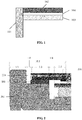
- FIG 1 is a first schematic diagram of a display assembly according to an exemplary embodiment. As shown in FIG 1 , the display assembly comprises:
- the display assembly may be applied to terminal devices.
- the terminal devices comprise mobile terminals and fixed terminals.
- the mobile terminals comprise, but are not limited to, mobile phones, tablet computers, notebook computers, and the like.
- the fixed terminals comprise, but are not limited to, television devices, desktop computers, and the like.
- the frame is a frame body that surrounds a terminal device and is exposed outside.
- the frame may be a frame body made of metals, plastics, or synthetic materials containing glass and plastics.
- a width of the frame may be 3.3 mm or 0.6 mm, which is not limited by the embodiments of the application.
- the liquid crystal panel is configured to display information.
- the frame may form an accommodating space, and the liquid crystal panel is embedded in the accommodating space.
- the glass diffusion plate is configured to diffuse light, so that transmitted light are evenly dispersed.
- the glass diffusion plate is attached to the light incident surface of the liquid crystal panel.
- the light incident surface of the liquid crystal panel is an opposite surface of the light exiting surface of the liquid crystal panel.
- the glass diffusion plate has high strength and is not easy to be deformed.
- the glass diffusion plate may also be configured to support the liquid crystal panel.
- the glass diffusion plate made of glass materials in the embodiments of the application has high strength and is not easy to be deformed, which may reduce the situation that the expansion gap inside the glass diffusion plate is large due to environmental changes, and may realize better support for the liquid crystal panel.
- the film structure is attached between the liquid crystal panel and the glass diffusion plate, for brightening the display effect of the display assembly.
- the film structure comprises, but is not limited to, a brightness enhancement film and a diffusion film.
- the brightness enhancement film comprises, but is not limited to, a lens or a light converging sheet.
- the light incident surface is a surface through which light enters
- the light exiting surface is a surface from which light exits.
- the light incident surface of the liquid crystal panel is a surface through which light enters the liquid crystal panel
- the light incident surface of the film structure is a surface through which light enters the film structure
- the light exiting surface of the film structure is a surface from which light exits the film structure.
- each of the liquid crystal panel, the glass diffusion plate and the film structure is oppositely arranged surfaces.
- the width of the frame is 3.3 mm
- a width of the black region of the liquid crystal panel is 6.5 mm
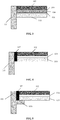
- a gap 204 between the liquid crystal panel 201 and the frame 202 is 1 mm.
- the black region part of the liquid crystal panel 201 is adhered on the frame 202 through an adhesive tape 203 to fix the liquid crystal panel 201.
- An adhering width between the black region and the frame is 3.3 mm.
- the width of the black region of the liquid crystal panel is shortened from 6.5 mm to 0.9 mm
- a width of a non-display region outside a display region is up to 10.8 mm, so that there is a problem of low screen-to-body ratio.
- the embodiments of the application provide a display assembly.
- the width of the frame may be 0.6 mm, and the width of the black region of the liquid crystal panel may be 0.9 mm.
- the width of the non-display region outside the display region in the display assembly may approach 1.5 mm, so that the screen-to-body ratio may be increased through the embodiments of the application.
- the film structure is attached to the surface of the liquid crystal panel, and the glass diffusion plate is attached to the surface of the film structure.
- the black region is not directly supported through the frame to realize the assembly of the liquid crystal panel.
- the whole liquid crystal panel is indirectly supported through the glass diffusion plate to realize the assembly of the liquid crystal panel.
- the assembly manner of the liquid crystal panel may adapt to the trend of narrowing of the black region of the liquid crystal panel, so that the screen-to-body ratio of a display screen may be further improved, and the assembly of the liquid crystal panel has universality.
- a transparent first attaching layer 105 is disposed between the liquid crystal panel 102 and the film structure 104, and the first attaching layer 105 is configured to completely attach the film structure 104 to the light incident surface of the liquid crystal panel 102; and a transparent second attaching layer 106 is disposed between the film structure 104 and the glass diffusion plate 103, and the second attaching layer 106 is configured to completely attach the glass diffusion plate 103 to the light incident surface of the film structure 104.
- the film structure is attached to the light incident surface of the liquid crystal panel through the first attaching layer
- the glass diffusion plate is attached to the light incident surface of the film structure through the second attaching layer.
- Both the first attaching layer and the second attaching layer may be made of transparent adhesives.
- the transparent adhesives comprise, but are not limited to, optical adhesive.
- the attaching region comprises a middle region and an edge region, and the edge region is located at a periphery of the middle region.
- the complete attaching may comprise attaching to each region, that is, attaching to the middle region and the edge region, rather than only to the edge region.
- an area of a first attaching layer is greater than a preset first area threshold and less than or equal to a first area of the film structure facing the surface of the liquid crystal panel; and an area of a second attaching layer is greater than a preset second area threshold and less than or equal to a second area of the film structure facing the surface of the glass diffusion plate.
- the first area threshold may be greater than or equal to a half of the first area; and the second area threshold may be greater than or equal to a half of the second area.
- the liquid crystal panel, the film structure and the glass diffusion plate are completely attached.
- the glass diffusion plate is not easy to be deformed, the possibility of deformation of the film structure between the liquid crystal panel and the glass diffusion plate due to environmental influences may be reduced, so that the assembly reliability of the liquid crystal panel is higher.
- the display assembly further comprises: a bonding agent 107 located on an inner side of the frame 101 and configured to bind the side surfaces of the glass diffusion plate 103, the film structure 104 and the liquid crystal panel 102 to the frame 101.
- the step that the glass diffusion plate, the film structure and the liquid crystal panel are attached to the frame comprises the following operations: firstly, the liquid crystal panel, the glass diffusion plate and the film structure are attached; and then, the liquid crystal panel, the glass diffusion plate and the film structure which are attached together are bonded to the frame through the bonding agent.
- the bonding agent is made of adhesives.
- a bonding width of the bonding agent is positively related to a bonding strength of the bonding agent. Situations with a high requirement for bonding strength may be met by increasing the bonding width of the bonding agent.
- the bonding width of the bonding agent may be between 0.4 mm and 0.8 mm, which is not limited by the embodiments of the application.
- the bonding agent is coated on the frame through an adhesive dispensing process.
- a projection region of the attached liquid crystal panel, glass diffusion plate and film structure onto the frame can be applied with the adhesive through an adhesive dispensing machine.
- a length of the projection region on the frame is greater than or equal to a sum of a thickness of each of the liquid crystal panel, the film structure and the glass diffusion plate.
- coating the bonding agent through the adhesive dispensing process may realize precise dispensing to improve the assembly reliability of the display assembly.
- the bonding agent is a waterproof bonding agent.
- the waterproof bonding agent to fix the liquid crystal panel, the glass diffusion plate and the film structure, the water resistance of the display assembly may be improved.
- a lug boss 101a is formed on the frame 101 in a direction extending toward an inside of the frame; and the edge of the glass diffusion plate 103 is carried on the lug boss 101a.
- the edge of the glass diffusion plate is carried on the lug boss, and the glass diffusion plate may be supported through the lug boss, so that the glass diffusion plate can better support the liquid crystal panel, so as to improve the assembly strength of the liquid crystal panel.
- a black region 102a is formed on the liquid crystal panel 102; the black region 102a is located at the edge of the liquid crystal panel 102; and the projection of the lug boss 101a onto the liquid crystal panel 102 is located in the black region 102a.
- the black region is located at the edge of the liquid crystal panel and is configured to shield light so as to reduce light leakage at the edge of the liquid crystal panel.
- the black region may be formed by a black matrix, and the black region surrounds the edge region of the liquid crystal panel to form a closed ring.
- the display assembly further comprises:
- the liquid crystal panel is a liquid crystal-liquid crystal panel
- a backlight source adopted by the liquid crystal-liquid crystal panel can provide display light for the liquid crystal-liquid crystal panel through the light source component on the back plate.
- the back plate and the glass diffusion plate are respectively located on two opposite sides of the lug boss, and the light source component is located between the back plate and the glass diffusion plate.
- the back plate, the light source component, the glass diffusion plate, the film structure and the liquid crystal panel are assembled in a laminated manner to form a display assembly.
- the glass diffusion plate is configured to diffuse the display light generated by the light source component, so that the display light may be evenly dispersed.
- the light source component comprises: a plurality of point light sources (such as Light Emitting Diode (LED)) or a plurality of line light sources (such as Cold Cathode Fluorescent Lamp (CCFL)).
- a plurality of point light sources such as Light Emitting Diode (LED)
- a plurality of line light sources such as Cold Cathode Fluorescent Lamp (CCFL)
- the light source component is located below the liquid crystal panel instead of on the side, so the display assembly is a direct below display assembly.
- a light emitting surface of the light source component faces the glass diffusion plate, and there is no other optical film between the light source component and the glass diffusion plate.
- the other optical films comprise: a light guide sheet and/or a diffusion sheet.
- the display assembly further comprises: a diffusion sheet; the diffusion sheet is completely attached to the glass diffusion plate; and the film structure is completely attached to the glass diffusion plate, in which the diffusion sheet is located between the film structure and the glass diffusion plate.
- the display light may be further evenly dispersed, so that the display effect of the display assembly may be improved.
- a gap is formed between the light source component and the glass diffusion plate.
- the gap between the light source component and the glass diffusion plate is configured to provide a tolerance space for process errors of the light source component and the glass diffusion plate. Therefore, the assembly of the light source component and the glass diffusion plate may be facilitated.
- a gap is formed between the frame and the side edge of the light source component.
- the gap between the frame and the side edge of the light source component is configured to provide a tolerance space for process errors of the light source component and the frame. Therefore, the assembly of the light source component and the glass diffusion plate may be facilitated.
- the embodiments of the application further provide a terminal device.
- the terminal device comprises the display assembly in one or more of the above embodiments.
- the terminal device may be a wearable electronic device and a mobile terminal, the mobile terminal comprises a mobile phone, a notebook computer and a tablet computer, the wearable electronic device comprises a smart watch. They are not limited by the embodiments of the application.
- the glass diffusion plate is attached to the light incident surface of the liquid crystal panel, and the film structure is attached between the liquid crystal panel and the glass diffusion plate.
- the black region is no longer directly supported through the frame to realize the assembly of the liquid crystal panel.
- the whole liquid crystal panel is indirectly supported through the glass diffusion plate to realize the assembly of the liquid crystal panel.
- the assembly manner of the liquid crystal panel may adapt to the trend of narrowing of the black region of the liquid crystal panel, so that the assembly of the liquid crystal panel has universality.
- the embodiments of the application further provide a manufacturing method of a display assembly.
- the display assembly is a display assembly in one or more of the above embodiments, and the manufacturing method comprises the following steps:
- the film structure is attached to the light incident surface of the liquid crystal panel
- the glass diffusion plate is attached to the light incident surface of the film structure.
- the black region is not directly supported through the frame to realize the assembly of the liquid crystal panel.
- the whole liquid crystal panel is indirectly supported through the glass diffusion plate to realize the assembly of the liquid crystal panel.
- the support area may be increased, and the reliability of assembly of the display assembly may be improved.
- the assembly manner of the liquid crystal panel may adapt to the trend of narrowing of the black region of the liquid crystal panel, so that the assembly of the liquid crystal panel has universality.
- the step that the liquid crystal panel, the glass diffusion plate and the film structure which are attached together are installed in the frame comprises the following operations:
- the step that the film structure is attached to the light incident surface of the liquid crystal panel comprises the following operation: the film structure is completely attached to the light incident surface of the liquid crystal panel through a first bonding layer.
- the step that the glass diffusion plate is attached to the light incident surface of the film structure comprises the following operation: the glass diffusion plate is completely attached to the light incident surface of the film structure through a second bonding layer.
- the manufacturing method further comprises the following steps:
- the manufacturing method further comprises the following step: a projection of the lug boss onto the liquid crystal panel is disposed in a black region of the liquid crystal panel.
- the manufacturing method further comprises the following step: before the liquid crystal panel, the glass diffusion plate and the film structure which are attached together are installed, a back plate provided with a light source component is installed below the lug boss on the frame.
- the step that the liquid crystal panel, the glass diffusion plate and the film structure which are attached together are installed in the frame comprises the following operation: the liquid crystal panel, the glass diffusion plate and the film structure which are attached together are installed in the frame above the light source component.
- the step that the back plate provided with the light source component is installed below the lug boss on the frame comprises the following operations:
- the manufacturing method further comprises the following step: the light source component and the glass diffusion plate are adjusted to form a first gap between the light source component and the glass diffusion plate.
- FIG 9 is a block diagram of a terminal device according to an exemplary embodiment.
- the terminal device may be a mobile phone, a computer, a digital broadcast terminal, a messaging device, a game console, a tablet device, a medical device, a fitness device, a personal digital assistant, and the like.
- the terminal device may comprise one or more of the following components: a processing component 802, a memory 804, a power component 806, a multimedia component 808, an audio component 810, an Input/Output (I/O) interface 812, a sensor component 814, and a communication component 816.
- a processing component 802 a memory 804
- a power component 806 a multimedia component 808, an audio component 810, an Input/Output (I/O) interface 812, a sensor component 814, and a communication component 816.
- I/O Input/Output
- the processing component 802 typically controls overall operations of the terminal device, such as the operations associated with display, telephone calls, data communications, camera operations, and recording operations.
- the processing component 802 may comprise one or more processors 820 to execute instructions to perform all or part of the steps in the above method.
- the processing component 802 may comprise one or more assemblies to facilitate the interaction between the processing component 802 and other components.
- the processing component 802 may comprise a multimedia assembly to facilitate the interaction between the multimedia component 808 and the processing component 802.
- the memory 804 is configured to store various types of data to support the operation on the terminal device. Examples of such data comprise instructions for any applications or methods operated on the terminal device, contact data, phone book data, messages, pictures, videos, etc.
- the memory 804 may be implemented using any type of volatile or non-volatile memory devices, or a combination thereof, such as a Static Random Access Memory (SRAM), an Electrically Erasable Programmable Read-Only Memory (EEPROM), an Erasable Programmable Read-Only Memory (EPROM), a Programmable Read-Only Memory (PROM), a Read-Only Memory (ROM), a magnetic memory, a flash memory, a magnetic disk or an optical disk.
- SRAM Static Random Access Memory
- EEPROM Electrically Erasable Programmable Read-Only Memory
- EPROM Erasable Programmable Read-Only Memory
- PROM Programmable Read-Only Memory
- ROM Read-Only Memory
- the power component 806 provides power to various components of the terminal device.
- the power component 806 may comprise a power management system, one or more power sources, and any other components associated with the generation, management, and distribution of power in the terminal device.
- the multimedia component 808 comprises a display panel providing an output interface between the terminal device and a user.
- the display panel may comprise a Liquid Crystal Display (LCD) and a Touch Panel (TP). If the display panel comprises the TP, the display panel may be implemented as a touch screen to receive input signals from the user.
- the TP comprises one or more touch sensors to sense touches, slides, and gestures on the TP. The touch sensors may not only sense a boundary of a touch or slide action, but also sense a period of time and a pressure associated with the touch or slide action.
- the multimedia component 808 comprises a front camera and/or a rear camera. The front camera and/or the rear camera may receive external multimedia data while the terminal device is in an operation mode, such as a photographing mode or a video mode. Each of the front camera and the rear camera may be a fixed optical lens system or may have focus and optical zoom capabilities.
- the audio component 810 is configured to output and/or input audio signals.
- the audio component 810 comprises a microphone (MIC) configured to receive external audio signals when the terminal device is in an operation mode, such as a call mode, a recording mode, and a voice recognition mode.
- the received audio signals may be further stored in the memory 804 or transmitted via the communication component 816.
- the audio component 810 further comprises a speaker configured to output audio signals.
- the I/O interface 812 provides an interface between the processing component 802 and peripheral interface assemblies such as a keyboard, a click wheel, and buttons. These buttons may comprise, but are not limited to, a home button, a volume button, a starting button, and a locking button.
- the sensor component 814 comprises one or more sensors to provide status assessments of various aspects of the terminal device. For instance, the sensor component 814 may detect an open/closed status of the terminal device, relative positioning of components such as a display and a keypad of the terminal device, a change in position of the terminal device or a component of the terminal device, a presence or absence of user contact with the terminal device, an orientation or an acceleration/deceleration of the terminal device, and a change in temperature of the terminal device.
- the sensor component 814 may comprise a proximity sensor configured to detect the presence of nearby objects without any physical contact.
- the sensor component 814 may also comprise a light sensor, such as a CMOS or CCD image sensor, for use in imaging applications.
- the sensor component 814 may also comprise an acceleration sensor, a gyroscope sensor, a magnetic sensor, a pressure sensor, or a temperature sensor.
- the communication component 816 is configured to facilitate wired or wireless communication between the terminal device and other devices.
- the terminal device may access a wireless network based on a communication standard, such as WiFi, 2G or 3G, or a combination thereof.
- the communication component 816 receives broadcast signals or broadcast associated information from an external broadcast management system via a broadcast channel.
- the communication component 816 further comprises a Near Field Communication (NFC) assembly to facilitate short-range communications.
- NFC assembly may be implemented based on a Radio Frequency Identification (RFID) technology, an Infrared Data Association (IrDA) technology, an Ultra-Wideband (UWB) technology, a Bluetooth (BT) technology, and other technologies.
- RFID Radio Frequency Identification
- IrDA Infrared Data Association
- UWB Ultra-Wideband
- BT Bluetooth
- the terminal device may be implemented with one or more of an Application Specific Integrated Circuit (ASIC), a Digital Signal Processor (DSP), a Digital Signal Processing Device (DSPD), a Programmable Logic Device (PLD), a Field Programmable Gate Array (FPGA), a controller, a micro-controller, a micro-processor, or other electronic components, for performing the above method.
- ASIC Application Specific Integrated Circuit
- DSP Digital Signal Processor
- DSPD Digital Signal Processing Device
- PLD Programmable Logic Device
- FPGA Field Programmable Gate Array
- controller a micro-controller, a micro-processor, or other electronic components, for performing the above method.
Landscapes
- Physics & Mathematics (AREA)
- Nonlinear Science (AREA)
- Chemical & Material Sciences (AREA)
- Crystallography & Structural Chemistry (AREA)
- General Physics & Mathematics (AREA)
- Optics & Photonics (AREA)
- Mathematical Physics (AREA)
- Engineering & Computer Science (AREA)
- Manufacturing & Machinery (AREA)
- Devices For Indicating Variable Information By Combining Individual Elements (AREA)
- Liquid Crystal (AREA)
Abstract
Description
- The application relates to the field of electronic devices, and particularly relates to a display assembly, a terminal device, and a manufacturing method of the display assembly.
- With the continuous development of terminal devices and the continuous improvement of user needs, the terminal devices, such as television devices and smart phones are developing in the direction of a high screen-to-body ratio. A width of a black region of a liquid crystal panel on an existing terminal device may be 6.5 mm, and the black region may be directly supported by a frame to complete an assembly of the liquid crystal panel. However, as the width of the black region of the liquid crystal panel is shortened from 6.5 mm to 0.9 mm, the assembly of the liquid crystal panel by supporting the black region may have reduced assembly reliability of the liquid crystal panel.
- The application provides a display assembly, a terminal device, and a manufacturing method of the display assembly.
- According to a first aspect of the invention, a display assembly is provided, and the display assembly comprises:
- a frame (bezel);
- a liquid crystal panel installed in the frame;
- a glass diffusion plate attached to a light incident surface of the liquid crystal panel; and
- a film structure including one or more optical films and attached between the liquid crystal panel and the glass diffusion plate, in which a light incident surface of the film structure faces the glass diffusion plate, a light exiting surface of the film structure faces the light incident surface of the liquid crystal panel, and the liquid crystal panel, the glass diffusion plate and the film structure are attached together to form an integrated structure.
- In some embodiments, a transparent first attaching layer is disposed between the liquid crystal panel and the film structure, and the first attaching layer is configured to completely attach the film structure to the light incident surface of the liquid crystal panel; and
a transparent second attaching layer is disposed between the film structure and the glass diffusion plate, and the second attaching layer is configured to completely attach the glass diffusion plate to the light incident surface of the film structure. - In some embodiments, the display assembly may further comprise:
a bonding agent located on an inner side of the frame and configured to bond side surfaces of the glass diffusion plate, the film structure and the liquid crystal panel to the frame. - In some embodiments, the bonding agent is coated on the frame through an adhesive dispensing process.
- In some embodiments, a lug boss extending toward an inside of the frame is formed on the frame; and
an edge of the glass diffusion plate is carried on the lug boss. - In some embodiments, a black region is formed on the liquid crystal panel;
the black region is located at the edge of the liquid crystal panel; and
a projection of the lug boss onto the liquid crystal panel is located in the black region. - In some embodiments, the display assembly may further comprise:
- a back plate located below the lug boss; and
- a light source component installed on the back plate and located between a back surface of the glass diffusion plate and the back plate.
- In some embodiments, a gap is formed between the light source component and the glass diffusion plate.
- In some embodiments, a gap is formed between the frame and a side edge of the light source component.
- According to a second aspect of the invention, a terminal device is provided, and the terminal device comprises the display assembly in the above first aspect.
- According to a third aspect of the invention, a manufacturing method of a display assembly is provided, the display assembly is the display assembly described in the above first aspect, and the manufacturing method comprises the following steps:
- a film structure is attached to a light incident surface of a liquid crystal panel;
- a glass diffusion plate is attached to a light incident surface of the film structure, in which the film structure is located between the liquid crystal panel and the glass diffusion plate, and a light exiting surface of the film structure faces the light incident surface of the liquid crystal panel; and
- the liquid crystal panel, the glass diffusion plate and the film structure which are attached together are installed in a frame.
- In some embodiments, the step that the liquid crystal panel, the glass diffusion plate and the film structure which are attached together are installed in the frame comprises the following operations:
- a bonding agent is coated on the frame through an adhesive dispensing process; and
- side surfaces of the liquid crystal panel, the glass diffusion plate and the film structure which are attached together are bonded in the frame through the bonding agent.
- In some embodiments, the step that the film structure is attached to the light incident surface of the liquid crystal panel comprises the following operation:
- the film structure is completely attached to the light incident surface of the liquid crystal panel through a first bonding layer;
- and the step that the glass diffusion plate is attached to the light incident surface of the film structure comprises the following operation:
the glass diffusion plate is completely attached to the light incident surface of the film structure through a second bonding layer. - In some embodiments, the manufacturing method may further comprise the following steps:
- a lug boss extending toward an inside of the frame is formed on the frame; and
- the edge of the glass diffusion plate is disposed between the lug boss and the liquid crystal panel so as to enable the lug boss to support the glass diffusion plate.
- In some embodiments, the manufacturing method may further comprise the following step:
the projection of the lug boss onto the liquid crystal panel is disposed in the black region of the liquid crystal panel. - In some embodiments, the manufacturing method may further comprise the following step:
- before the liquid crystal panel, the glass diffusion plate and the film structure which are attached together are installed, a back plate provided with a light source component is installed below the lug boss on the frame;
- and the step that the liquid crystal panel, the glass diffusion plate and the film structure which are attached together are installed in the frame comprises the following operation:
- the liquid crystal panel, the glass diffusion plate and the film structure which are attached together are installed in the frame above the light source component.
- The technical solutions provided by the embodiments of the application may have the following beneficial effects:
In the embodiments of the application, the glass diffusion plate is attached to the light incident surface of the liquid crystal panel, and the film structure is attached between the liquid crystal panel and the glass diffusion plate. In other words, in the embodiments of the application, the black region is no longer directly supported and fixed through the frame to realize the assembly of the liquid crystal panel. Instead, the whole liquid crystal panel is indirectly supported through the glass diffusion plate to realize the assembly of the liquid crystal panel. In this way, the support area may be increased, and the reliability of assembly of the display assembly may be improved. Furthermore, in the embodiments of the application, the assembly manner of the liquid crystal panel may adapt to the trend of narrowing of the black region of the liquid crystal panel, so that the screen-to-body ratio of a display screen may be further improved so as to enable the assembly of the liquid crystal panel to have universality. - It should be understood that the above general description and the following detailed description are merely exemplary and explanatory.
- The accompanying drawings, which are incorporated in and constitute a part of this specification, illustrate embodiments consistent with the application and, together with the description, serve to explain the principles of the application.
-
FIG 1 is a first schematic diagram of a display assembly according to an exemplary embodiment. -
FIG 2 is a second schematic diagram of a display assembly according to an exemplary embodiment. -
FIG 3 is a third schematic diagram of a display assembly according to an exemplary embodiment. -
FIG 4 is a fourth schematic diagram of a display assembly according to an exemplary embodiment. -
FIG 5 is a fifth schematic diagram of a display assembly according to an exemplary embodiment. -
FIG 6 is a sixth schematic diagram of a display assembly according to an exemplary embodiment. -
FIG 7 is a seventh schematic diagram of a display assembly according to an exemplary embodiment. -
FIG 8 is a flow chart of a manufacturing process of a display assembly according to an exemplary embodiment. -
FIG 9 is a block diagram of a terminal device according to an exemplary embodiment. - Reference will now be made in detail to exemplary embodiments, examples of which are illustrated in the accompanying drawings. The following description refers to the accompanying drawings in which the same numbers in different drawings represent the same or similar elements unless otherwise represented. The implementations set forth in the following description of exemplary embodiments do not represent all implementations consistent with the application. Instead, they are merely examples of apparatuses and methods consistent with aspects related to the application as recited in the appended claims.
-
FIG 1 is a first schematic diagram of a display assembly according to an exemplary embodiment. As shown inFIG 1 , the display assembly comprises: - a
frame 101; - a
liquid crystal panel 102 installed in the frame; - a
glass diffusion plate 103 attached to a light incident surface of theliquid crystal panel 102; and - a
film structure 104 including one or more optical films and attached between theliquid crystal panel 102 and theglass diffusion plate 103, in which a light incident surface of thefilm structure 104 faces theglass diffusion plate 103, a light exiting surface of thefilm structure 104 faces the light incident surface of theliquid crystal panel 102, and theliquid crystal panel 102, theglass diffusion plate 103 and thefilm structure 104 are attached together to form an integrated structure. - In the embodiments of the application, the display assembly may be applied to terminal devices. The terminal devices comprise mobile terminals and fixed terminals. The mobile terminals comprise, but are not limited to, mobile phones, tablet computers, notebook computers, and the like. The fixed terminals comprise, but are not limited to, television devices, desktop computers, and the like.
- The frame is a frame body that surrounds a terminal device and is exposed outside. The frame may be a frame body made of metals, plastics, or synthetic materials containing glass and plastics.
- It should be noted that a width of the frame may be 3.3 mm or 0.6 mm, which is not limited by the embodiments of the application.
- The liquid crystal panel is configured to display information.
- In the embodiments of the application, the frame may form an accommodating space, and the liquid crystal panel is embedded in the accommodating space.
- The glass diffusion plate is configured to diffuse light, so that transmitted light are evenly dispersed. The glass diffusion plate is attached to the light incident surface of the liquid crystal panel. The light incident surface of the liquid crystal panel is an opposite surface of the light exiting surface of the liquid crystal panel.
- In the embodiments of the application, the glass diffusion plate has high strength and is not easy to be deformed. The glass diffusion plate may also be configured to support the liquid crystal panel.
- It should be noted that compared with the existing diffusion plates made of plastic materials, the glass diffusion plate made of glass materials in the embodiments of the application has high strength and is not easy to be deformed, which may reduce the situation that the expansion gap inside the glass diffusion plate is large due to environmental changes, and may realize better support for the liquid crystal panel.
- The film structure is attached between the liquid crystal panel and the glass diffusion plate, for brightening the display effect of the display assembly.
- It should be noted that the film structure comprises, but is not limited to, a brightness enhancement film and a diffusion film. The brightness enhancement film comprises, but is not limited to, a lens or a light converging sheet.
- In the embodiments of the application, the light incident surface is a surface through which light enters, and the light exiting surface is a surface from which light exits. For example, the light incident surface of the liquid crystal panel is a surface through which light enters the liquid crystal panel; the light incident surface of the film structure is a surface through which light enters the film structure; and the light exiting surface of the film structure is a surface from which light exits the film structure.
- It should be noted that the light incident surface and the light exiting surface of each of the liquid crystal panel, the glass diffusion plate and the film structure are oppositely arranged surfaces.
- In related technologies, as shown in
FIG 2 , the width of the frame is 3.3 mm, a width of the black region of the liquid crystal panel is 6.5 mm, and agap 204 between theliquid crystal panel 201 and theframe 202 is 1 mm. The black region part of theliquid crystal panel 201 is adhered on theframe 202 through anadhesive tape 203 to fix theliquid crystal panel 201. An adhering width between the black region and the frame is 3.3 mm. However, when the width of the black region of the liquid crystal panel is shortened from 6.5 mm to 0.9 mm, if the frame and the black region of the liquid crystal panel are adhered directly through an adhesive tape, there is a problem that the assembly stability of the liquid crystal panel is reduced due to the decrease in the adhering width. Furthermore, a width of a non-display region outside a display region is up to 10.8 mm, so that there is a problem of low screen-to-body ratio. - Based on this, the embodiments of the application provide a display assembly. In the display assembly, the width of the frame may be 0.6 mm, and the width of the black region of the liquid crystal panel may be 0.9 mm. The width of the non-display region outside the display region in the display assembly may approach 1.5 mm, so that the screen-to-body ratio may be increased through the embodiments of the application.
- Furthermore, in the embodiments of the application, the film structure is attached to the surface of the liquid crystal panel, and the glass diffusion plate is attached to the surface of the film structure. In other words, in the embodiments of the application, the black region is not directly supported through the frame to realize the assembly of the liquid crystal panel. Instead, the whole liquid crystal panel is indirectly supported through the glass diffusion plate to realize the assembly of the liquid crystal panel. In this way, the support area may be increased, and the reliability of assembly of the display assembly may be improved. Furthermore, in the embodiments of the application, the assembly manner of the liquid crystal panel may adapt to the trend of narrowing of the black region of the liquid crystal panel, so that the screen-to-body ratio of a display screen may be further improved, and the assembly of the liquid crystal panel has universality.
- In some embodiments, as shown in
FIG 3 , a transparent first attachinglayer 105 is disposed between theliquid crystal panel 102 and thefilm structure 104, and the first attachinglayer 105 is configured to completely attach thefilm structure 104 to the light incident surface of theliquid crystal panel 102; and
a transparent second attachinglayer 106 is disposed between thefilm structure 104 and theglass diffusion plate 103, and the second attachinglayer 106 is configured to completely attach theglass diffusion plate 103 to the light incident surface of thefilm structure 104. - In the embodiments of the application, the film structure is attached to the light incident surface of the liquid crystal panel through the first attaching layer, and the glass diffusion plate is attached to the light incident surface of the film structure through the second attaching layer. Both the first attaching layer and the second attaching layer may be made of transparent adhesives. The transparent adhesives comprise, but are not limited to, optical adhesive.
- It should be noted that the liquid crystal panel, the film structure and the glass diffusion plate are completely attached together. The attaching region comprises a middle region and an edge region, and the edge region is located at a periphery of the middle region. The complete attaching may comprise attaching to each region, that is, attaching to the middle region and the edge region, rather than only to the edge region.
- In some embodiments, an area of a first attaching layer is greater than a preset first area threshold and less than or equal to a first area of the film structure facing the surface of the liquid crystal panel; and an area of a second attaching layer is greater than a preset second area threshold and less than or equal to a second area of the film structure facing the surface of the glass diffusion plate.
- Exemplarily, the first area threshold may be greater than or equal to a half of the first area; and the second area threshold may be greater than or equal to a half of the second area.
- It can be understood that in the embodiments of the application, the liquid crystal panel, the film structure and the glass diffusion plate are completely attached. Through the characteristic that the glass diffusion plate is not easy to be deformed, the possibility of deformation of the film structure between the liquid crystal panel and the glass diffusion plate due to environmental influences may be reduced, so that the assembly reliability of the liquid crystal panel is higher.
- In some embodiments, as shown in
FIG 4 , the display assembly further comprises:
abonding agent 107 located on an inner side of theframe 101 and configured to bind the side surfaces of theglass diffusion plate 103, thefilm structure 104 and theliquid crystal panel 102 to theframe 101. - In the embodiments of the application, the step that the glass diffusion plate, the film structure and the liquid crystal panel are attached to the frame comprises the following operations: firstly, the liquid crystal panel, the glass diffusion plate and the film structure are attached; and then, the liquid crystal panel, the glass diffusion plate and the film structure which are attached together are bonded to the frame through the bonding agent.
- It should be noted that the bonding agent is made of adhesives. A bonding width of the bonding agent is positively related to a bonding strength of the bonding agent. Situations with a high requirement for bonding strength may be met by increasing the bonding width of the bonding agent.
- Exemplarily, the bonding width of the bonding agent may be between 0.4 mm and 0.8 mm, which is not limited by the embodiments of the application.
- In some embodiments, the bonding agent is coated on the frame through an adhesive dispensing process.
- In the embodiments of the application, a projection region of the attached liquid crystal panel, glass diffusion plate and film structure onto the frame can be applied with the adhesive through an adhesive dispensing machine. A length of the projection region on the frame is greater than or equal to a sum of a thickness of each of the liquid crystal panel, the film structure and the glass diffusion plate.
- It can be understood that coating the bonding agent through the adhesive dispensing process may realize precise dispensing to improve the assembly reliability of the display assembly.
- In some other embodiments, the bonding agent is a waterproof bonding agent.
- It should be noted that by using the waterproof bonding agent to fix the liquid crystal panel, the glass diffusion plate and the film structure, the water resistance of the display assembly may be improved.
- In some embodiments, as shown in
FIG 5 , alug boss 101a is formed on theframe 101 in a direction extending toward an inside of the frame; and
the edge of theglass diffusion plate 103 is carried on thelug boss 101a. - In the embodiments of the application, the edge of the glass diffusion plate is carried on the lug boss, and the glass diffusion plate may be supported through the lug boss, so that the glass diffusion plate can better support the liquid crystal panel, so as to improve the assembly strength of the liquid crystal panel.
- In some embodiments, as shown in
FIG. 6 , ablack region 102a is formed on theliquid crystal panel 102;
theblack region 102a is located at the edge of theliquid crystal panel 102; and
the projection of thelug boss 101a onto theliquid crystal panel 102 is located in theblack region 102a. - The black region is located at the edge of the liquid crystal panel and is configured to shield light so as to reduce light leakage at the edge of the liquid crystal panel.
- The black region may be formed by a black matrix, and the black region surrounds the edge region of the liquid crystal panel to form a closed ring.
- In the embodiments of the application, the projection of the lug boss onto the liquid crystal panel is located in a region where the black region is located. In other words, the black region can also be configured to shield the lug boss to reduce exposure of the lug in a display region of the liquid crystal panel, so that the display region of the liquid crystal panel may be increased.
- In some embodiments, as shown in
FIG 7 , the display assembly further comprises: - a
back plate 108 located below thelug boss 101a; and - a
light source component 109 installed on theback plate 108 and located between theglass diffusion plate 103 and theback plate 108. - In other words, in the embodiments of the application, the liquid crystal panel is a liquid crystal-liquid crystal panel, and a backlight source adopted by the liquid crystal-liquid crystal panel can provide display light for the liquid crystal-liquid crystal panel through the light source component on the back plate.
- It should be noted that the back plate and the glass diffusion plate are respectively located on two opposite sides of the lug boss, and the light source component is located between the back plate and the glass diffusion plate. In the embodiments of the application, the back plate, the light source component, the glass diffusion plate, the film structure and the liquid crystal panel are assembled in a laminated manner to form a display assembly.
- The glass diffusion plate is configured to diffuse the display light generated by the light source component, so that the display light may be evenly dispersed.
- The light source component comprises: a plurality of point light sources (such as Light Emitting Diode (LED)) or a plurality of line light sources (such as Cold Cathode Fluorescent Lamp (CCFL)).
- In the embodiments of the application, the light source component is located below the liquid crystal panel instead of on the side, so the display assembly is a direct below display assembly.
- In some embodiments, a light emitting surface of the light source component faces the glass diffusion plate, and there is no other optical film between the light source component and the glass diffusion plate. For example, the other optical films comprise: a light guide sheet and/or a diffusion sheet.
- In some other embodiments, the display assembly further comprises: a diffusion sheet; the diffusion sheet is completely attached to the glass diffusion plate; and the film structure is completely attached to the glass diffusion plate, in which the diffusion sheet is located between the film structure and the glass diffusion plate.
- It should be noted that by completely attaching the diffusion sheet to the glass diffusion plate, the display light may be further evenly dispersed, so that the display effect of the display assembly may be improved.
- In some embodiments, a gap is formed between the light source component and the glass diffusion plate.
- In the embodiments of the application, the gap between the light source component and the glass diffusion plate is configured to provide a tolerance space for process errors of the light source component and the glass diffusion plate. Therefore, the assembly of the light source component and the glass diffusion plate may be facilitated.
- In some embodiments, a gap is formed between the frame and the side edge of the light source component.
- In the embodiments of the application, the gap between the frame and the side edge of the light source component is configured to provide a tolerance space for process errors of the light source component and the frame. Therefore, the assembly of the light source component and the glass diffusion plate may be facilitated.
- The embodiments of the application further provide a terminal device. The terminal device comprises the display assembly in one or more of the above embodiments.
- The terminal device may be a wearable electronic device and a mobile terminal, the mobile terminal comprises a mobile phone, a notebook computer and a tablet computer, the wearable electronic device comprises a smart watch. They are not limited by the embodiments of the application.
- It can be understood that in the terminal device of the embodiments of the application, the glass diffusion plate is attached to the light incident surface of the liquid crystal panel, and the film structure is attached between the liquid crystal panel and the glass diffusion plate. In other words, in the embodiments of the application, the black region is no longer directly supported through the frame to realize the assembly of the liquid crystal panel. Instead, the whole liquid crystal panel is indirectly supported through the glass diffusion plate to realize the assembly of the liquid crystal panel. In this way, the support area may be increased, and the reliability of assembly of the display assembly may be improved. Furthermore, in the embodiments of the application, the assembly manner of the liquid crystal panel may adapt to the trend of narrowing of the black region of the liquid crystal panel, so that the assembly of the liquid crystal panel has universality.
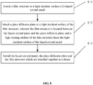
- The embodiments of the application further provide a manufacturing method of a display assembly. As shown in
FIG 8 , the display assembly is a display assembly in one or more of the above embodiments, and the manufacturing method comprises the following steps: - S11, a film structure is attached to a light incident surface of a liquid crystal panel;
- S12, a glass diffusion plate is attached to a light incident surface of the film structure, in which the film structure is located between the liquid crystal panel and the glass diffusion plate, and a light exiting surface of the film structure faces the light incident surface of the liquid crystal panel; and
- S13, the liquid crystal panel, the glass diffusion plate and the film structure which are attached together are installed in a frame.
- It can be understood that in the embodiments of the application, the film structure is attached to the light incident surface of the liquid crystal panel, and the glass diffusion plate is attached to the light incident surface of the film structure. In other words, in the embodiments of the application, the black region is not directly supported through the frame to realize the assembly of the liquid crystal panel. Instead the whole liquid crystal panel is indirectly supported through the glass diffusion plate to realize the assembly of the liquid crystal panel. In this way, the support area may be increased, and the reliability of assembly of the display assembly may be improved. Furthermore, in the embodiments of the application, the assembly manner of the liquid crystal panel may adapt to the trend of narrowing of the black region of the liquid crystal panel, so that the assembly of the liquid crystal panel has universality.
- In some embodiments, the step that the liquid crystal panel, the glass diffusion plate and the film structure which are attached together are installed in the frame comprises the following operations:
- a bonding agent is coated on the frame through an adhesive dispensing process; and
- side surfaces of the liquid crystal panel, the glass diffusion plate and the film structure which are attached together are bonded in the frame through the bonding agent.
- In some embodiments, the step that the film structure is attached to the light incident surface of the liquid crystal panel comprises the following operation:
the film structure is completely attached to the light incident surface of the liquid crystal panel through a first bonding layer. - The step that the glass diffusion plate is attached to the light incident surface of the film structure comprises the following operation:
the glass diffusion plate is completely attached to the light incident surface of the film structure through a second bonding layer. - In some embodiments, the manufacturing method further comprises the following steps:
- a lug boss is formed on the frame in a direction extending into inside of the frame; and
- an edge of the glass diffusion plate is disposed between the lug boss and the liquid crystal panel so as to enable the lug boss to support the glass diffusion plate.
- In some embodiments, the manufacturing method further comprises the following step:
a projection of the lug boss onto the liquid crystal panel is disposed in a black region of the liquid crystal panel. - In some embodiments, the manufacturing method further comprises the following step:
before the liquid crystal panel, the glass diffusion plate and the film structure which are attached together are installed, a back plate provided with a light source component is installed below the lug boss on the frame. - The step that the liquid crystal panel, the glass diffusion plate and the film structure which are attached together are installed in the frame comprises the following operation:
the liquid crystal panel, the glass diffusion plate and the film structure which are attached together are installed in the frame above the light source component. - In some embodiments, the step that the back plate provided with the light source component is installed below the lug boss on the frame comprises the following operations:
- the light source component is installed on the back plate and is aligned with the lug boss, and a second gap is formed between the light source component and the frame; and
- the installed back plate and light source component are disposed below the lug boss on the frame.
- In some embodiments, the manufacturing method further comprises the following step:
the light source component and the glass diffusion plate are adjusted to form a first gap between the light source component and the glass diffusion plate. - With respect to the manufacturing methods in the above embodiments, the implementation manner of the manufacturing method in each embodiment has been described in detail in each embodiment of the display assembly manufactured by the manufacturing method, and will not be repeated here.
- It should be noted that the "first" and "second" in the embodiments of the application are only for convenience of expression and distinction, and have no other specific meanings.
-
FIG 9 is a block diagram of a terminal device according to an exemplary embodiment. For example, the terminal device may be a mobile phone, a computer, a digital broadcast terminal, a messaging device, a game console, a tablet device, a medical device, a fitness device, a personal digital assistant, and the like. - Referring to
FIG 9 , the terminal device may comprise one or more of the following components: aprocessing component 802, amemory 804, apower component 806, amultimedia component 808, anaudio component 810, an Input/Output (I/O)interface 812, asensor component 814, and acommunication component 816. - The
processing component 802 typically controls overall operations of the terminal device, such as the operations associated with display, telephone calls, data communications, camera operations, and recording operations. Theprocessing component 802 may comprise one ormore processors 820 to execute instructions to perform all or part of the steps in the above method. Moreover, theprocessing component 802 may comprise one or more assemblies to facilitate the interaction between theprocessing component 802 and other components. For instance, theprocessing component 802 may comprise a multimedia assembly to facilitate the interaction between themultimedia component 808 and theprocessing component 802. - The
memory 804 is configured to store various types of data to support the operation on the terminal device. Examples of such data comprise instructions for any applications or methods operated on the terminal device, contact data, phone book data, messages, pictures, videos, etc. Thememory 804 may be implemented using any type of volatile or non-volatile memory devices, or a combination thereof, such as a Static Random Access Memory (SRAM), an Electrically Erasable Programmable Read-Only Memory (EEPROM), an Erasable Programmable Read-Only Memory (EPROM), a Programmable Read-Only Memory (PROM), a Read-Only Memory (ROM), a magnetic memory, a flash memory, a magnetic disk or an optical disk. - The
power component 806 provides power to various components of the terminal device. Thepower component 806 may comprise a power management system, one or more power sources, and any other components associated with the generation, management, and distribution of power in the terminal device. - The
multimedia component 808 comprises a display panel providing an output interface between the terminal device and a user. In some embodiments, the display panel may comprise a Liquid Crystal Display (LCD) and a Touch Panel (TP). If the display panel comprises the TP, the display panel may be implemented as a touch screen to receive input signals from the user. The TP comprises one or more touch sensors to sense touches, slides, and gestures on the TP. The touch sensors may not only sense a boundary of a touch or slide action, but also sense a period of time and a pressure associated with the touch or slide action. In some embodiments, themultimedia component 808 comprises a front camera and/or a rear camera. The front camera and/or the rear camera may receive external multimedia data while the terminal device is in an operation mode, such as a photographing mode or a video mode. Each of the front camera and the rear camera may be a fixed optical lens system or may have focus and optical zoom capabilities. - The
audio component 810 is configured to output and/or input audio signals. For example, theaudio component 810 comprises a microphone (MIC) configured to receive external audio signals when the terminal device is in an operation mode, such as a call mode, a recording mode, and a voice recognition mode. The received audio signals may be further stored in thememory 804 or transmitted via thecommunication component 816. In some embodiments, theaudio component 810 further comprises a speaker configured to output audio signals. - The I/
O interface 812 provides an interface between theprocessing component 802 and peripheral interface assemblies such as a keyboard, a click wheel, and buttons. These buttons may comprise, but are not limited to, a home button, a volume button, a starting button, and a locking button. - The
sensor component 814 comprises one or more sensors to provide status assessments of various aspects of the terminal device. For instance, thesensor component 814 may detect an open/closed status of the terminal device, relative positioning of components such as a display and a keypad of the terminal device, a change in position of the terminal device or a component of the terminal device, a presence or absence of user contact with the terminal device, an orientation or an acceleration/deceleration of the terminal device, and a change in temperature of the terminal device. Thesensor component 814 may comprise a proximity sensor configured to detect the presence of nearby objects without any physical contact. Thesensor component 814 may also comprise a light sensor, such as a CMOS or CCD image sensor, for use in imaging applications. In some embodiments, thesensor component 814 may also comprise an acceleration sensor, a gyroscope sensor, a magnetic sensor, a pressure sensor, or a temperature sensor. - The
communication component 816 is configured to facilitate wired or wireless communication between the terminal device and other devices. The terminal device may access a wireless network based on a communication standard, such as WiFi, 2G or 3G, or a combination thereof. In an exemplary embodiment, thecommunication component 816 receives broadcast signals or broadcast associated information from an external broadcast management system via a broadcast channel. In an exemplary embodiment, thecommunication component 816 further comprises a Near Field Communication (NFC) assembly to facilitate short-range communications. For example, the NFC assembly may be implemented based on a Radio Frequency Identification (RFID) technology, an Infrared Data Association (IrDA) technology, an Ultra-Wideband (UWB) technology, a Bluetooth (BT) technology, and other technologies. - In exemplary embodiments, the terminal device may be implemented with one or more of an Application Specific Integrated Circuit (ASIC), a Digital Signal Processor (DSP), a Digital Signal Processing Device (DSPD), a Programmable Logic Device (PLD), a Field Programmable Gate Array (FPGA), a controller, a micro-controller, a micro-processor, or other electronic components, for performing the above method.
- Other embodiments of the application will be apparent to those skilled in the art from consideration of the specification and practice of the application here. This application is intended to cover any variations, uses, or adaptations of the application following the general principles thereof and including such departures from the application as come within known or customary practice in the art. It is intended that the specification and embodiments be considered as exemplary only, with a true scope of the application being indicated by the following claims.
- It will be appreciated that the application is not limited to the exact construction that has been described above and illustrated in the accompanying drawings, and that various modifications and changes can be made without departing from the scope thereof. It is intended that the scope of the application only be limited by the appended claims.
Claims (15)
- A display assembly, characterized in that the display assembly comprises:a frame (101);a liquid crystal panel (102) installed in the frame (101);a glass diffusion plate (103) attached to a light incident surface of the liquid crystal panel (102); anda film structure (104) comprising one or more optical films and attached between the liquid crystal panel (102) and the glass diffusion plate (103), wherein a light incident surface of the film structure (104) faces the glass diffusion plate (103), a light exiting surface of the film structure (104) faces the light incident surface of the liquid crystal panel (102), and the liquid crystal panel (102), the glass diffusion plate (103) and the film structure (104)are attached together to form an integrated structure.
- The display assembly of claim 1, wherein a transparent first attaching layer (105) is disposed between the liquid crystal panel (102) and the film structure (104), and the first attaching layer (105) is configured to completely attach the film structure (104) to the light incident surface of the liquid crystal panel (102); and
a transparent second attaching layer (106) is disposed between the film structure (104) and the glass diffusion plate (103), and the second attaching layer (106) is configured to completely attach the glass diffusion plate (103) to the light incident surface of the film structure (104). - The display assembly of claim 1 or 2, further comprising:
a bonding agent (107) located on an inner side of the frame (101) and configured to bond side surfaces of the glass diffusion plate (103), the film structure (104) and the liquid crystal panel (102) to the frame (101). - The display assembly of claim 3, wherein the bonding agent (104) is coated on the frame (101) through an adhesive dispensing process.
- The display assembly of any one of the preceding claims, wherein a lug boss (101a) extending toward an inside of the frame (101) is formed on the frame (101); and
an edge of the glass diffusion plate (103) is carried on the lug boss (101a). - The display assembly of claim 5, wherein a black region (102a) is formed on the liquid crystal panel (102);the black region (102a) is located at an edge of the liquid crystal panel (102); anda projection of the lug boss (101a) onto the liquid crystal panel (102) is located in the black region (102a).
- The display assembly of claim 5 or 6, further comprising:a back plate (108)located below the lug boss (101a); anda light source component (109) installed on the back plate (108) and located between the glass diffusion plate (103) and the back plate (108).
- The display assembly of claim 7, wherein a gap is formed between the light source component (109) and the glass diffusion plate (103), and/or
a gap is formed between the frame (101) and a side edge of the light source component (109). - A terminal device, characterized in that the terminal device comprises the display assembly of any one of claims 1 to 8.
- A manufacturing method of a display assembly of any one of claims 1 to 8, characterized in that the manufacturing method comprises:attaching the film structure (104) to the light incident surface of the liquid crystal panel (102);attaching the glass diffusion plate (103) to the light incident surface of the film structure (104), wherein the film structure (104) is located between the liquid crystal panel (102) and the glass diffusion plate (103), and the light exiting surface of the film structure (104) faces the light incident surface of the liquid crystal panel (102); andand installing the liquid crystal panel (102), the glass diffusion plate (103) and the film structure (104) which are attached together in the frame.
- The manufacturing method of claim 10, wherein the step of installing the liquid crystal panel (102), the glass diffusion plate (103) and the film structure (104)which are attached together in the frame comprises:coating a bonding agent (107) on the frame (101) through an adhesive dispensing process; andbonding side surfaces of the liquid crystal panel (102), the glass diffusion plate (103) and the film structure (104) which are attached together in the frame through the bonding agent (107).
- The manufacturing method of claim 10 or 11, wherein the step of attaching the film structure (104) to the light incident surface of the liquid crystal panel (102) comprises:completely attaching the film structure (104) to the light incident surface of the liquid crystal panel (102) through a first bonding layer;and wherein the step of attaching the glass diffusion plate (103) to the light incident surface of the film structure (104) comprises:
completely attaching the glass diffusion plate (103) to the light incident surface of the film structure (104) through a second bonding layer. - The manufacturing method of claim 10 or 11, further comprising:forming a lug boss (101a), extending in a direction toward an inside of the frame (101), on the frame (101); anddisposing an edge of the glass diffusion plate (103) between the lug boss (101a) and the liquid crystal panel (102) to enable the lug boss (101a) to support the glass diffusion plate (103).
- The manufacturing method of claim 13, further comprising:
disposing a projection of the lug boss (101a) onto the liquid crystal panel (102) in a black region (102a) of the liquid crystal panel (102). - The manufacturing method of claim 13, further comprising:before installing the liquid crystal panel (102), the glass diffusion plate (103) and the film structure (104) which are attached together, installing a back plate (108) provided with a light source component (109) below the lug boss (101a) on the frame (101);and wherein the step of installing the liquid crystal panel (102), the glass diffusion plate (103) and the film structure (104) which are attached together in the frame (101) comprises:
installing the liquid crystal panel (102), the glass diffusion plate (103) and the film structure (104) which are attached together in the frame (101) above the light source component (109).
Applications Claiming Priority (1)
| Application Number | Priority Date | Filing Date | Title |
|---|---|---|---|
| CN202010568211.0A CN111624798A (en) | 2020-06-19 | 2020-06-19 | Display module, terminal equipment and manufacturing method of display module |
Publications (1)
| Publication Number | Publication Date |
|---|---|
| EP3926394A1 true EP3926394A1 (en) | 2021-12-22 |
Family
ID=72258366
Family Applications (1)
| Application Number | Title | Priority Date | Filing Date |
|---|---|---|---|
| EP21151773.5A Pending EP3926394A1 (en) | 2020-06-19 | 2021-01-15 | Display assembly, terminal device, and manufacturing method of display assembly |
Country Status (5)
| Country | Link |
|---|---|
| US (1) | US11681172B2 (en) |
| EP (1) | EP3926394A1 (en) |
| JP (1) | JP7241107B2 (en) |
| KR (1) | KR102475592B1 (en) |
| CN (1) | CN111624798A (en) |
Families Citing this family (2)
| Publication number | Priority date | Publication date | Assignee | Title |
|---|---|---|---|---|
| CN114258218B (en) * | 2020-09-25 | 2024-06-04 | 北京小米移动软件有限公司 | Electronic devices and electronic device middle frames |
| TWI879239B (en) * | 2023-11-20 | 2025-04-01 | 達擎股份有限公司 | Display panel |
Citations (3)
| Publication number | Priority date | Publication date | Assignee | Title |
|---|---|---|---|---|
| US20160202537A1 (en) * | 2015-01-14 | 2016-07-14 | Samsung Display Co., Ltd. | Display apparatus |
| US20180164619A1 (en) * | 2016-12-13 | 2018-06-14 | Lg Display Co., Ltd. | Electronic device |
| US20200124904A1 (en) * | 2011-12-30 | 2020-04-23 | Samsung Electronics Co., Ltd. | Display device |
Family Cites Families (16)
| Publication number | Priority date | Publication date | Assignee | Title |
|---|---|---|---|---|
| US7436473B2 (en) | 2002-11-27 | 2008-10-14 | Samsung Electronics Co., Ltd. | Liquid crystal display and manufacturing method thereof |
| JP3790246B2 (en) * | 2003-05-26 | 2006-06-28 | 住友ゴム工業株式会社 | Liquid crystal display |
| KR20060005154A (en) * | 2004-07-12 | 2006-01-17 | 삼성전자주식회사 | Back light assembly and display device having same |
| US7948572B2 (en) * | 2006-07-21 | 2011-05-24 | Samsung Electronics Co., Ltd. | Hollow mold for receiving liquid crystal panel and diffuser plate and liquid crystal display including hollow mold |
| KR20110052071A (en) * | 2009-11-12 | 2011-05-18 | 엘지전자 주식회사 | LCD Display |
| US20130257705A1 (en) | 2012-03-27 | 2013-10-03 | Yajun Yu | Backlight Module and LCD Device |
| CN202580954U (en) * | 2012-04-26 | 2012-12-05 | 贵阳海信电子有限公司 | Backlight module and television |
| KR101347566B1 (en) * | 2012-05-01 | 2014-01-06 | 엘지디스플레이 주식회사 | Display apparatus and method for manufacturing the same |
| KR102136203B1 (en) * | 2014-02-03 | 2020-08-14 | 삼성디스플레이 주식회사 | Backlight unit and liquid crystal display comprising the same |
| CN107966843B (en) * | 2016-10-20 | 2021-03-26 | 群创光电股份有限公司 | display device |
| CN109164630A (en) * | 2018-10-24 | 2019-01-08 | 京东方科技集团股份有限公司 | Display module and display panel |
| CN111458918A (en) * | 2019-01-21 | 2020-07-28 | 鸿富锦精密工业(深圳)有限公司 | display screen |
| CN209446932U (en) * | 2019-02-27 | 2019-09-27 | 东莞市银泰丰光学科技有限公司 | A TV display module with a fully bonded glass light guide plate structure |
| CN209657040U (en) * | 2019-05-05 | 2019-11-19 | 深圳市沣视科技有限公司 | A kind of highlighted liquid-crystal displaying screen structure |
| CN110927845A (en) | 2019-12-10 | 2020-03-27 | 合肥泰沃达智能装备有限公司 | Straight following formula glass diffuser plate |
| CN212276168U (en) * | 2020-06-19 | 2021-01-01 | 北京小米移动软件有限公司 | A display module and terminal equipment |
-
2020
- 2020-06-19 CN CN202010568211.0A patent/CN111624798A/en active Pending
- 2020-11-27 KR KR1020200161804A patent/KR102475592B1/en active Active
-
2021
- 2021-01-12 US US17/146,897 patent/US11681172B2/en active Active
- 2021-01-15 EP EP21151773.5A patent/EP3926394A1/en active Pending
- 2021-02-09 JP JP2021018658A patent/JP7241107B2/en active Active
Patent Citations (3)
| Publication number | Priority date | Publication date | Assignee | Title |
|---|---|---|---|---|
| US20200124904A1 (en) * | 2011-12-30 | 2020-04-23 | Samsung Electronics Co., Ltd. | Display device |
| US20160202537A1 (en) * | 2015-01-14 | 2016-07-14 | Samsung Display Co., Ltd. | Display apparatus |
| US20180164619A1 (en) * | 2016-12-13 | 2018-06-14 | Lg Display Co., Ltd. | Electronic device |
Also Published As
| Publication number | Publication date |
|---|---|
| CN111624798A (en) | 2020-09-04 |
| KR102475592B1 (en) | 2022-12-08 |
| JP7241107B2 (en) | 2023-03-16 |
| US20210397037A1 (en) | 2021-12-23 |
| US11681172B2 (en) | 2023-06-20 |
| JP2022001932A (en) | 2022-01-06 |
| KR20210157287A (en) | 2021-12-28 |
Similar Documents
| Publication | Publication Date | Title |
|---|---|---|
| KR102263465B1 (en) | Display module, display device, display device control method and storage medium | |
| US10907077B1 (en) | Method and device of attaching flexible screen to cover plate and terminal | |
| US10785352B2 (en) | Front case of electronic device, and electronic device | |
| US11681172B2 (en) | Display assembly, terminal device, and manufacturing method of display assembly | |
| CN111182399A (en) | Earphone sound guide assembly and terminal equipment | |
| US9244490B2 (en) | Mobile terminal | |
| JP7203878B2 (en) | Display device and display device manufacturing method | |
| KR101971964B1 (en) | MOBILE TERMINAL and METHODE FOR PRODUCING DISPLAY UNIT | |
| CN211830844U (en) | Electronic device | |
| CN212276168U (en) | A display module and terminal equipment | |
| KR101962127B1 (en) | Display module and mobile terminal having it | |
| CN112987159A (en) | Polaroid, display screen device and mobile terminal | |
| US10935850B1 (en) | Display panel, manufacturing method, and electronic device | |
| CN212905555U (en) | Backlight Modules and Electronic Equipment | |
| CN114002873B (en) | Electronic device, control method thereof, and computer-readable storage medium | |
| CN112014917B (en) | Polarizers, Displays and Terminals | |
| US11419183B2 (en) | Outer frame, terminal housing and terminal | |
| KR20120021065A (en) | Mobile terminal | |
| CN112684630A (en) | Backlight module assembly method, backlight module and terminal equipment | |
| CN223377867U (en) | Display assembly and electronic equipment | |
| CN219225821U (en) | Display devices and electronic equipment | |
| CN219936618U (en) | A screen module and electronic device | |
| CN223758330U (en) | Camera components and electronic devices | |
| CN219287559U (en) | Electronic equipment | |
| CN217932353U (en) | Backlight module and display module |
Legal Events
| Date | Code | Title | Description |
|---|---|---|---|
| PUAI | Public reference made under article 153(3) epc to a published international application that has entered the european phase |
Free format text: ORIGINAL CODE: 0009012 |
|
| STAA | Information on the status of an ep patent application or granted ep patent |
Free format text: STATUS: THE APPLICATION HAS BEEN PUBLISHED |
|
| AK | Designated contracting states |
Kind code of ref document: A1 Designated state(s): AL AT BE BG CH CY CZ DE DK EE ES FI FR GB GR HR HU IE IS IT LI LT LU LV MC MK MT NL NO PL PT RO RS SE SI SK SM TR |
|
| B565 | Issuance of search results under rule 164(2) epc |
Effective date: 20210630 |
|
| STAA | Information on the status of an ep patent application or granted ep patent |
Free format text: STATUS: REQUEST FOR EXAMINATION WAS MADE |
|
| 17P | Request for examination filed |
Effective date: 20220613 |
|
| RBV | Designated contracting states (corrected) |
Designated state(s): AL AT BE BG CH CY CZ DE DK EE ES FI FR GB GR HR HU IE IS IT LI LT LU LV MC MK MT NL NO PL PT RO RS SE SI SK SM TR |
|
| STAA | Information on the status of an ep patent application or granted ep patent |
Free format text: STATUS: EXAMINATION IS IN PROGRESS |
|
| 17Q | First examination report despatched |
Effective date: 20241212 |