EP3925819B1 - Power supply ensuring system and power supply ensuring method - Google Patents
Power supply ensuring system and power supply ensuring method Download PDFInfo
- Publication number
- EP3925819B1 EP3925819B1 EP20841021.7A EP20841021A EP3925819B1 EP 3925819 B1 EP3925819 B1 EP 3925819B1 EP 20841021 A EP20841021 A EP 20841021A EP 3925819 B1 EP3925819 B1 EP 3925819B1
- Authority
- EP
- European Patent Office
- Prior art keywords
- module
- high voltage
- power supply
- electrical energy
- power
- Prior art date
- Legal status (The legal status is an assumption and is not a legal conclusion. Google has not performed a legal analysis and makes no representation as to the accuracy of the status listed.)
- Active
Links
Images


Classifications
-
- G—PHYSICS
- G06—COMPUTING OR CALCULATING; COUNTING
- G06F—ELECTRIC DIGITAL DATA PROCESSING
- G06F1/00—Details not covered by groups G06F3/00 - G06F13/00 and G06F21/00
- G06F1/26—Power supply means, e.g. regulation thereof
- G06F1/32—Means for saving power
- G06F1/3203—Power management, i.e. event-based initiation of a power-saving mode
- G06F1/3206—Monitoring of events, devices or parameters that trigger a change in power modality
- G06F1/3212—Monitoring battery levels, e.g. power saving mode being initiated when battery voltage goes below a certain level
-
- H—ELECTRICITY
- H02—GENERATION; CONVERSION OR DISTRIBUTION OF ELECTRIC POWER
- H02M—APPARATUS FOR CONVERSION BETWEEN AC AND AC, BETWEEN AC AND DC, OR BETWEEN DC AND DC, AND FOR USE WITH MAINS OR SIMILAR POWER SUPPLY SYSTEMS; CONVERSION OF DC OR AC INPUT POWER INTO SURGE OUTPUT POWER; CONTROL OR REGULATION THEREOF
- H02M1/00—Details of apparatus for conversion
- H02M1/0003—Details of control, feedback or regulation circuits
- H02M1/0006—Arrangements for supplying an adequate voltage to the control circuit of converters
-
- B—PERFORMING OPERATIONS; TRANSPORTING
- B60—VEHICLES IN GENERAL
- B60L—PROPULSION OF ELECTRICALLY-PROPELLED VEHICLES; SUPPLYING ELECTRIC POWER FOR AUXILIARY EQUIPMENT OF ELECTRICALLY-PROPELLED VEHICLES; ELECTRODYNAMIC BRAKE SYSTEMS FOR VEHICLES IN GENERAL; MAGNETIC SUSPENSION OR LEVITATION FOR VEHICLES; MONITORING OPERATING VARIABLES OF ELECTRICALLY-PROPELLED VEHICLES; ELECTRIC SAFETY DEVICES FOR ELECTRICALLY-PROPELLED VEHICLES
- B60L58/00—Methods or circuit arrangements for monitoring or controlling batteries or fuel cells, specially adapted for electric vehicles
- B60L58/10—Methods or circuit arrangements for monitoring or controlling batteries or fuel cells, specially adapted for electric vehicles for monitoring or controlling batteries
- B60L58/12—Methods or circuit arrangements for monitoring or controlling batteries or fuel cells, specially adapted for electric vehicles for monitoring or controlling batteries responding to state of charge [SoC]
-
- B—PERFORMING OPERATIONS; TRANSPORTING
- B60—VEHICLES IN GENERAL
- B60L—PROPULSION OF ELECTRICALLY-PROPELLED VEHICLES; SUPPLYING ELECTRIC POWER FOR AUXILIARY EQUIPMENT OF ELECTRICALLY-PROPELLED VEHICLES; ELECTRODYNAMIC BRAKE SYSTEMS FOR VEHICLES IN GENERAL; MAGNETIC SUSPENSION OR LEVITATION FOR VEHICLES; MONITORING OPERATING VARIABLES OF ELECTRICALLY-PROPELLED VEHICLES; ELECTRIC SAFETY DEVICES FOR ELECTRICALLY-PROPELLED VEHICLES
- B60L53/00—Methods of charging batteries, specially adapted for electric vehicles; Charging stations or on-board charging equipment therefor; Exchange of energy storage elements in electric vehicles
- B60L53/20—Methods of charging batteries, specially adapted for electric vehicles; Charging stations or on-board charging equipment therefor; Exchange of energy storage elements in electric vehicles characterised by converters located in the vehicle
- B60L53/22—Constructional details or arrangements of charging converters specially adapted for charging electric vehicles
-
- B—PERFORMING OPERATIONS; TRANSPORTING
- B60—VEHICLES IN GENERAL
- B60L—PROPULSION OF ELECTRICALLY-PROPELLED VEHICLES; SUPPLYING ELECTRIC POWER FOR AUXILIARY EQUIPMENT OF ELECTRICALLY-PROPELLED VEHICLES; ELECTRODYNAMIC BRAKE SYSTEMS FOR VEHICLES IN GENERAL; MAGNETIC SUSPENSION OR LEVITATION FOR VEHICLES; MONITORING OPERATING VARIABLES OF ELECTRICALLY-PROPELLED VEHICLES; ELECTRIC SAFETY DEVICES FOR ELECTRICALLY-PROPELLED VEHICLES
- B60L58/00—Methods or circuit arrangements for monitoring or controlling batteries or fuel cells, specially adapted for electric vehicles
- B60L58/10—Methods or circuit arrangements for monitoring or controlling batteries or fuel cells, specially adapted for electric vehicles for monitoring or controlling batteries
-
- B—PERFORMING OPERATIONS; TRANSPORTING
- B60—VEHICLES IN GENERAL
- B60L—PROPULSION OF ELECTRICALLY-PROPELLED VEHICLES; SUPPLYING ELECTRIC POWER FOR AUXILIARY EQUIPMENT OF ELECTRICALLY-PROPELLED VEHICLES; ELECTRODYNAMIC BRAKE SYSTEMS FOR VEHICLES IN GENERAL; MAGNETIC SUSPENSION OR LEVITATION FOR VEHICLES; MONITORING OPERATING VARIABLES OF ELECTRICALLY-PROPELLED VEHICLES; ELECTRIC SAFETY DEVICES FOR ELECTRICALLY-PROPELLED VEHICLES
- B60L58/00—Methods or circuit arrangements for monitoring or controlling batteries or fuel cells, specially adapted for electric vehicles
- B60L58/10—Methods or circuit arrangements for monitoring or controlling batteries or fuel cells, specially adapted for electric vehicles for monitoring or controlling batteries
- B60L58/18—Methods or circuit arrangements for monitoring or controlling batteries or fuel cells, specially adapted for electric vehicles for monitoring or controlling batteries of two or more battery modules
- B60L58/20—Methods or circuit arrangements for monitoring or controlling batteries or fuel cells, specially adapted for electric vehicles for monitoring or controlling batteries of two or more battery modules having different nominal voltages
-
- G—PHYSICS
- G06—COMPUTING OR CALCULATING; COUNTING
- G06F—ELECTRIC DIGITAL DATA PROCESSING
- G06F1/00—Details not covered by groups G06F3/00 - G06F13/00 and G06F21/00
- G06F1/16—Constructional details or arrangements
- G06F1/1613—Constructional details or arrangements for portable computers
- G06F1/1633—Constructional details or arrangements of portable computers not specific to the type of enclosures covered by groups G06F1/1615 - G06F1/1626
- G06F1/1635—Details related to the integration of battery packs and other power supplies such as fuel cells or integrated AC adapter
-
- H—ELECTRICITY
- H01—ELECTRIC ELEMENTS
- H01M—PROCESSES OR MEANS, e.g. BATTERIES, FOR THE DIRECT CONVERSION OF CHEMICAL ENERGY INTO ELECTRICAL ENERGY
- H01M10/00—Secondary cells; Manufacture thereof
- H01M10/42—Methods or arrangements for servicing or maintenance of secondary cells or secondary half-cells
- H01M10/425—Structural combination with electronic components, e.g. electronic circuits integrated to the outside of the casing
- H01M10/4257—Smart batteries, e.g. electronic circuits inside the housing of the cells or batteries
-
- H—ELECTRICITY
- H02—GENERATION; CONVERSION OR DISTRIBUTION OF ELECTRIC POWER
- H02M—APPARATUS FOR CONVERSION BETWEEN AC AND AC, BETWEEN AC AND DC, OR BETWEEN DC AND DC, AND FOR USE WITH MAINS OR SIMILAR POWER SUPPLY SYSTEMS; CONVERSION OF DC OR AC INPUT POWER INTO SURGE OUTPUT POWER; CONTROL OR REGULATION THEREOF
- H02M3/00—Conversion of DC power input into DC power output
- H02M3/22—Conversion of DC power input into DC power output with intermediate conversion into AC
- H02M3/24—Conversion of DC power input into DC power output with intermediate conversion into AC by static converters
- H02M3/28—Conversion of DC power input into DC power output with intermediate conversion into AC by static converters using discharge tubes with control electrode or semiconductor devices with control electrode to produce the intermediate AC
- H02M3/325—Conversion of DC power input into DC power output with intermediate conversion into AC by static converters using discharge tubes with control electrode or semiconductor devices with control electrode to produce the intermediate AC using devices of a triode or a transistor type requiring continuous application of a control signal
- H02M3/335—Conversion of DC power input into DC power output with intermediate conversion into AC by static converters using discharge tubes with control electrode or semiconductor devices with control electrode to produce the intermediate AC using devices of a triode or a transistor type requiring continuous application of a control signal using semiconductor devices only
- H02M3/33538—Conversion of DC power input into DC power output with intermediate conversion into AC by static converters using discharge tubes with control electrode or semiconductor devices with control electrode to produce the intermediate AC using devices of a triode or a transistor type requiring continuous application of a control signal using semiconductor devices only of the forward type
- H02M3/33546—Conversion of DC power input into DC power output with intermediate conversion into AC by static converters using discharge tubes with control electrode or semiconductor devices with control electrode to produce the intermediate AC using devices of a triode or a transistor type requiring continuous application of a control signal using semiconductor devices only of the forward type with automatic control of the output voltage or current
- H02M3/33553—Conversion of DC power input into DC power output with intermediate conversion into AC by static converters using discharge tubes with control electrode or semiconductor devices with control electrode to produce the intermediate AC using devices of a triode or a transistor type requiring continuous application of a control signal using semiconductor devices only of the forward type with automatic control of the output voltage or current with galvanic isolation between input and output of both the power stage and the feedback loop
-
- B—PERFORMING OPERATIONS; TRANSPORTING
- B60—VEHICLES IN GENERAL
- B60L—PROPULSION OF ELECTRICALLY-PROPELLED VEHICLES; SUPPLYING ELECTRIC POWER FOR AUXILIARY EQUIPMENT OF ELECTRICALLY-PROPELLED VEHICLES; ELECTRODYNAMIC BRAKE SYSTEMS FOR VEHICLES IN GENERAL; MAGNETIC SUSPENSION OR LEVITATION FOR VEHICLES; MONITORING OPERATING VARIABLES OF ELECTRICALLY-PROPELLED VEHICLES; ELECTRIC SAFETY DEVICES FOR ELECTRICALLY-PROPELLED VEHICLES
- B60L2240/00—Control parameters of input or output; Target parameters
- B60L2240/40—Drive Train control parameters
- B60L2240/54—Drive Train control parameters related to batteries
- B60L2240/547—Voltage
-
- H—ELECTRICITY
- H01—ELECTRIC ELEMENTS
- H01M—PROCESSES OR MEANS, e.g. BATTERIES, FOR THE DIRECT CONVERSION OF CHEMICAL ENERGY INTO ELECTRICAL ENERGY
- H01M10/00—Secondary cells; Manufacture thereof
- H01M10/42—Methods or arrangements for servicing or maintenance of secondary cells or secondary half-cells
- H01M10/425—Structural combination with electronic components, e.g. electronic circuits integrated to the outside of the casing
- H01M2010/4271—Battery management systems including electronic circuits, e.g. control of current or voltage to keep battery in healthy state, cell balancing
-
- H—ELECTRICITY
- H01—ELECTRIC ELEMENTS
- H01M—PROCESSES OR MEANS, e.g. BATTERIES, FOR THE DIRECT CONVERSION OF CHEMICAL ENERGY INTO ELECTRICAL ENERGY
- H01M10/00—Secondary cells; Manufacture thereof
- H01M10/42—Methods or arrangements for servicing or maintenance of secondary cells or secondary half-cells
- H01M10/425—Structural combination with electronic components, e.g. electronic circuits integrated to the outside of the casing
- H01M2010/4278—Systems for data transfer from batteries, e.g. transfer of battery parameters to a controller, data transferred between battery controller and main controller
-
- H—ELECTRICITY
- H01—ELECTRIC ELEMENTS
- H01M—PROCESSES OR MEANS, e.g. BATTERIES, FOR THE DIRECT CONVERSION OF CHEMICAL ENERGY INTO ELECTRICAL ENERGY
- H01M2220/00—Batteries for particular applications
- H01M2220/20—Batteries in motive systems, e.g. vehicle, ship, plane
-
- H—ELECTRICITY
- H02—GENERATION; CONVERSION OR DISTRIBUTION OF ELECTRIC POWER
- H02M—APPARATUS FOR CONVERSION BETWEEN AC AND AC, BETWEEN AC AND DC, OR BETWEEN DC AND DC, AND FOR USE WITH MAINS OR SIMILAR POWER SUPPLY SYSTEMS; CONVERSION OF DC OR AC INPUT POWER INTO SURGE OUTPUT POWER; CONTROL OR REGULATION THEREOF
- H02M1/00—Details of apparatus for conversion
- H02M1/0003—Details of control, feedback or regulation circuits
- H02M1/0032—Control circuits allowing low power mode operation, e.g. in standby mode
-
- H—ELECTRICITY
- H02—GENERATION; CONVERSION OR DISTRIBUTION OF ELECTRIC POWER
- H02M—APPARATUS FOR CONVERSION BETWEEN AC AND AC, BETWEEN AC AND DC, OR BETWEEN DC AND DC, AND FOR USE WITH MAINS OR SIMILAR POWER SUPPLY SYSTEMS; CONVERSION OF DC OR AC INPUT POWER INTO SURGE OUTPUT POWER; CONTROL OR REGULATION THEREOF
- H02M1/00—Details of apparatus for conversion
- H02M1/0045—Converters combining the concepts of switch-mode regulation and linear regulation, e.g. linear pre-regulator to switching converter, linear and switching converter in parallel, same converter or same transistor operating either in linear or switching mode
-
- H—ELECTRICITY
- H02—GENERATION; CONVERSION OR DISTRIBUTION OF ELECTRIC POWER
- H02M—APPARATUS FOR CONVERSION BETWEEN AC AND AC, BETWEEN AC AND DC, OR BETWEEN DC AND DC, AND FOR USE WITH MAINS OR SIMILAR POWER SUPPLY SYSTEMS; CONVERSION OF DC OR AC INPUT POWER INTO SURGE OUTPUT POWER; CONTROL OR REGULATION THEREOF
- H02M1/00—Details of apparatus for conversion
- H02M1/14—Arrangements for reducing ripples from DC input or output
-
- H—ELECTRICITY
- H02—GENERATION; CONVERSION OR DISTRIBUTION OF ELECTRIC POWER
- H02M—APPARATUS FOR CONVERSION BETWEEN AC AND AC, BETWEEN AC AND DC, OR BETWEEN DC AND DC, AND FOR USE WITH MAINS OR SIMILAR POWER SUPPLY SYSTEMS; CONVERSION OF DC OR AC INPUT POWER INTO SURGE OUTPUT POWER; CONTROL OR REGULATION THEREOF
- H02M1/00—Details of apparatus for conversion
- H02M1/32—Means for protecting converters other than automatic disconnection
- H02M1/34—Snubber circuits
- H02M1/344—Active dissipative snubbers
-
- H—ELECTRICITY
- H02—GENERATION; CONVERSION OR DISTRIBUTION OF ELECTRIC POWER
- H02M—APPARATUS FOR CONVERSION BETWEEN AC AND AC, BETWEEN AC AND DC, OR BETWEEN DC AND DC, AND FOR USE WITH MAINS OR SIMILAR POWER SUPPLY SYSTEMS; CONVERSION OF DC OR AC INPUT POWER INTO SURGE OUTPUT POWER; CONTROL OR REGULATION THEREOF
- H02M1/00—Details of apparatus for conversion
- H02M1/36—Means for starting or stopping converters
-
- H—ELECTRICITY
- H02—GENERATION; CONVERSION OR DISTRIBUTION OF ELECTRIC POWER
- H02M—APPARATUS FOR CONVERSION BETWEEN AC AND AC, BETWEEN AC AND DC, OR BETWEEN DC AND DC, AND FOR USE WITH MAINS OR SIMILAR POWER SUPPLY SYSTEMS; CONVERSION OF DC OR AC INPUT POWER INTO SURGE OUTPUT POWER; CONTROL OR REGULATION THEREOF
- H02M3/00—Conversion of DC power input into DC power output
- H02M3/22—Conversion of DC power input into DC power output with intermediate conversion into AC
- H02M3/24—Conversion of DC power input into DC power output with intermediate conversion into AC by static converters
- H02M3/28—Conversion of DC power input into DC power output with intermediate conversion into AC by static converters using discharge tubes with control electrode or semiconductor devices with control electrode to produce the intermediate AC
- H02M3/325—Conversion of DC power input into DC power output with intermediate conversion into AC by static converters using discharge tubes with control electrode or semiconductor devices with control electrode to produce the intermediate AC using devices of a triode or a transistor type requiring continuous application of a control signal
- H02M3/335—Conversion of DC power input into DC power output with intermediate conversion into AC by static converters using discharge tubes with control electrode or semiconductor devices with control electrode to produce the intermediate AC using devices of a triode or a transistor type requiring continuous application of a control signal using semiconductor devices only
- H02M3/33569—Conversion of DC power input into DC power output with intermediate conversion into AC by static converters using discharge tubes with control electrode or semiconductor devices with control electrode to produce the intermediate AC using devices of a triode or a transistor type requiring continuous application of a control signal using semiconductor devices only having several active switching elements
- H02M3/33576—Conversion of DC power input into DC power output with intermediate conversion into AC by static converters using discharge tubes with control electrode or semiconductor devices with control electrode to produce the intermediate AC using devices of a triode or a transistor type requiring continuous application of a control signal using semiconductor devices only having several active switching elements having at least one active switching element at the secondary side of an isolation transformer
- H02M3/33592—Conversion of DC power input into DC power output with intermediate conversion into AC by static converters using discharge tubes with control electrode or semiconductor devices with control electrode to produce the intermediate AC using devices of a triode or a transistor type requiring continuous application of a control signal using semiconductor devices only having several active switching elements having at least one active switching element at the secondary side of an isolation transformer having a synchronous rectifier circuit or a synchronous freewheeling circuit at the secondary side of an isolation transformer
-
- Y—GENERAL TAGGING OF NEW TECHNOLOGICAL DEVELOPMENTS; GENERAL TAGGING OF CROSS-SECTIONAL TECHNOLOGIES SPANNING OVER SEVERAL SECTIONS OF THE IPC; TECHNICAL SUBJECTS COVERED BY FORMER USPC CROSS-REFERENCE ART COLLECTIONS [XRACs] AND DIGESTS
- Y02—TECHNOLOGIES OR APPLICATIONS FOR MITIGATION OR ADAPTATION AGAINST CLIMATE CHANGE
- Y02E—REDUCTION OF GREENHOUSE GAS [GHG] EMISSIONS, RELATED TO ENERGY GENERATION, TRANSMISSION OR DISTRIBUTION
- Y02E60/00—Enabling technologies; Technologies with a potential or indirect contribution to GHG emissions mitigation
- Y02E60/10—Energy storage using batteries
-
- Y—GENERAL TAGGING OF NEW TECHNOLOGICAL DEVELOPMENTS; GENERAL TAGGING OF CROSS-SECTIONAL TECHNOLOGIES SPANNING OVER SEVERAL SECTIONS OF THE IPC; TECHNICAL SUBJECTS COVERED BY FORMER USPC CROSS-REFERENCE ART COLLECTIONS [XRACs] AND DIGESTS
- Y02—TECHNOLOGIES OR APPLICATIONS FOR MITIGATION OR ADAPTATION AGAINST CLIMATE CHANGE
- Y02T—CLIMATE CHANGE MITIGATION TECHNOLOGIES RELATED TO TRANSPORTATION
- Y02T10/00—Road transport of goods or passengers
- Y02T10/60—Other road transportation technologies with climate change mitigation effect
- Y02T10/70—Energy storage systems for electromobility, e.g. batteries
-
- Y—GENERAL TAGGING OF NEW TECHNOLOGICAL DEVELOPMENTS; GENERAL TAGGING OF CROSS-SECTIONAL TECHNOLOGIES SPANNING OVER SEVERAL SECTIONS OF THE IPC; TECHNICAL SUBJECTS COVERED BY FORMER USPC CROSS-REFERENCE ART COLLECTIONS [XRACs] AND DIGESTS
- Y02—TECHNOLOGIES OR APPLICATIONS FOR MITIGATION OR ADAPTATION AGAINST CLIMATE CHANGE
- Y02T—CLIMATE CHANGE MITIGATION TECHNOLOGIES RELATED TO TRANSPORTATION
- Y02T10/00—Road transport of goods or passengers
- Y02T10/60—Other road transportation technologies with climate change mitigation effect
- Y02T10/7072—Electromobility specific charging systems or methods for batteries, ultracapacitors, supercapacitors or double-layer capacitors
-
- Y—GENERAL TAGGING OF NEW TECHNOLOGICAL DEVELOPMENTS; GENERAL TAGGING OF CROSS-SECTIONAL TECHNOLOGIES SPANNING OVER SEVERAL SECTIONS OF THE IPC; TECHNICAL SUBJECTS COVERED BY FORMER USPC CROSS-REFERENCE ART COLLECTIONS [XRACs] AND DIGESTS
- Y02—TECHNOLOGIES OR APPLICATIONS FOR MITIGATION OR ADAPTATION AGAINST CLIMATE CHANGE
- Y02T—CLIMATE CHANGE MITIGATION TECHNOLOGIES RELATED TO TRANSPORTATION
- Y02T90/00—Enabling technologies or technologies with a potential or indirect contribution to GHG emissions mitigation
- Y02T90/10—Technologies relating to charging of electric vehicles
- Y02T90/14—Plug-in electric vehicles
Definitions
- This application relates to the field of battery management, and in particular, to a power supply guarantee system and a power supply guarantee method.
- a battery management system is an important integral part of energy management of a new energy vehicle and implements intelligent management and maintenance for a power battery system of the electric vehicles.
- a vehicle lead-acid battery provides a power supply for the BMS, and is connected to a low-voltage controller through a power supply bus to power the low-voltage controller.
- a conventional power supply system once the lead-acid battery is absent in the electric vehicle and the BMS is in a sleep state, the BMS will not work normally.
- CN 108 215 915 A discloses an electric energy transmission circuit and device.
- the electric energy transmission circuit comprises a wake-up sub-circuit, a high-voltage control sub-circuit and a power conversion sub-circuit.
- CN 106026712 A discloses a switching power supply, especially a secondary-side control method and a secondary-side control circuit of an isolated switching power supply.
- An embodiment of this application provides a power supply guarantee system and a power supply guarantee method to keep providing a power supply to a BMS when the BMS is in a sleep state, so that the BMS is always in a powered state and normal operation of the BMS is ensured.
- a power supply guarantee system is provided, and applied to a BMS.
- the power supply guarantee system of the invention comprises the features recited in independent claim 1.
- a power supply guarantee method is provided, and applied to the power supply guarantee system described above, and the power supply guarantee method comprises the steps recited in claim 14.
- the BMS when the BMS is in a sleep state, the BMS is periodically woken up to ensure that the BMS is in a powered state, and to facilitate the BMS to collect and store relevant information in the battery pack of an integrated vehicle.
- the BMS is woken up without resorting to a vehicle lead-acid battery, thereby reducing the loss of lead acid and increasing the life of the lead acid.
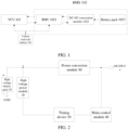
- FIG. 1 is a schematic structural diagram of a system in which a BMS is powered by a vehicle lead-acid battery according to an embodiment of this application.
- the vehicle lead-acid battery 101 may power a BMS 102.
- the BMS 102 may include a battery management unit (BMU) 1021, a DC-DC conversion module 1022, and a battery pack 1023.
- the DC-DC conversion module 1022 can perform voltage conversion, for example, convert a 24 V system power supply into a 12 V supply to power 12 V-enabled electrical devices in a vehicle.
- the vehicle lead-acid battery 101 may provide a power supply to the BMS 102, and may also be connected to a low voltage control unit through a power supply bus to power the low voltage control unit.
- the BMS 102 exchanges information with a vehicle control unit (VCU) 103 through a controller area network (CAN) bus, and uploads relevant information such as a state of charge (SOC), voltage, and current of the battery pack 1023 to the VCU.
- VCU vehicle control unit
- CAN controller area network
- the VCU and the BMS are powered off. Without being powered by the lead-acid battery, the entire BMS is in a sleep state and unable to monitor the states such as SOC, voltage, and current of the battery pack in the integrated vehicle or to perform corresponding operations.
- an embodiment of this application provides a power supply guarantee system and a power supply guarantee method to provide a power source to the BMS.
- the BMS When the BMS is in a sleep state, the BMS is periodically woken up to ensure that the BMS is in a powered state, and to facilitate the BMS to collect and store relevant information in the battery pack of the integrated vehicle.
- the BMS With the power supply guarantee system and the power supply guarantee method according to the embodiments of this application, the BMS is woken up without resorting to a vehicle lead-acid battery, thereby reducing the loss of lead acid and increasing the life of the lead acid.
- FIG. 2 is a schematic structural diagram of a power supply guarantee system according to an embodiment of this application.
- a power supply guarantee system 200 in this embodiment of this application may include: a high voltage battery pack 10, a high voltage power module 20, a timing device 30, a main control module 40, and a power conversion module 50.
- the main control module 40 may be configured to send a received wake-up time to the timing device.
- the high voltage power module 20 is configured to power the timing device 30 according to electrical energy in the high voltage battery pack 10.
- the timing device 30 may be configured to set a wake-up clock according to the wake-up time, start timing when the BMS enters sleep, and send a discharge instruction to the high voltage battery pack 10 when the timing reaches the wake-up time.
- the power conversion module 50 is configured to convert high voltage electrical energy into low voltage electrical energy, and use the low voltage electrical energy to power the BMS, where the high voltage electrical energy is output by the high voltage battery pack 10 according to the discharge instruction.
- the wake-up time received by the timing device is a wake-up time that is set by the VCU.
- the VCU (not shown in FIG. 2 ) may be configured to set a wake-up time, and send the wake-up time to the timing device through the main control module.
- the main control module may be, for example, a microprogrammed control unit (microprogrammed control unit, MCU).
- the power supply guarantee system when the integrated vehicle contains no lead-acid battery and the BMS enters a sleep mode, the power supply can still be provided to the BMS, so that the BMS is always in a powered state and the entire BMS system keeps operating normally.
- FIG. 3 is a detailed schematic structural diagram of a power supply guarantee system according to another embodiment of this application.
- the reference numerals used in FIG. 3 to denote structures are the same as the reference numerals used in FIG. 2 for the same or equivalent structures. It needs to be noted that the embodiments are not intended to limit the scope of the disclosure of this application.
- the power conversion module 50 may specifically include: a forward power control module 51, a first high voltage transmission module, a synchronous rectification module 52, a first isolation and driving module 53, and a second high voltage transmission module.
- the timing device 30 is further configured to provide an enable signal to the forward power control module 51 when the timing reaches the wake-up time.
- the forward power control module 51 starts working under the control of enable signal.
- the forward power control module 51 is configured to provide a power supply to the synchronous rectification module 52 through the first high voltage transmission module, and control an on-state of connection between the high voltage battery pack 10 and the second high voltage transmission module through the first isolation and driving module 53.
- the second high voltage transmission module is configured to convert high voltage electrical energy in the high voltage battery pack 10 into low voltage electrical energy when the connection between the second high voltage transmission module and the high voltage battery pack 10 is turned on.
- the synchronous rectification module 52 is configured to perform synchronous rectification on the low voltage electrical energy, and use the synchronously rectified low voltage electrical energy to power the BMS.
- the VCU when the integrated vehicle needs to be powered off, the VCU can set the wake-up time in advance, generate a timed wake-up instruction according to the wake-up time, and deliver the wake-up instruction to the BMS, and then the VCU is powered off.
- the BMS delivers the timed wake-up instruction to the timing device through the main control module. After a timer sets a time, the entire BMS will enter a sleep state. When the timing of the timing device reaches the wake-up time, the timing device delivers a discharge command to the high voltage battery pack.
- the power conversion module converts electrical energy in the high voltage battery pack into low voltage electrical energy as a power source to the BMS, so that the BMS is woken up from sleep, and starts to monitor relevant information such as the SOC, voltage, and current in the battery pack of the integrated vehicle and perform corresponding operations.
- the high voltage power module includes a first power access point B, a first voltage divider resistor network R1, a second voltage divider resistor network R2, and a first voltage regulator unit DZ1.
- the timing device 30 includes a clock power supply end VCC1.
- the first power access point B is located at a positive electrode of the high voltage battery pack 10.
- One end of the first voltage divider resistor network R1 is connected to the first power access point B.
- the other end of the first voltage divider resistor network R1 is connected to one end of the second voltage divider resistor network R2.
- the other end of the second voltage divider resistor network R2 is connected to the clock power supply end VCC1.
- One end of the first voltage regulator unit DZ1 is connected to the clock power supply end VCC1.
- the other end of the first voltage regulator unit DZ1 is connected to a reference voltage end.
- the first voltage divider resistor network R1 and the second voltage divider resistor network R2 may each include a plurality of serial-connected resistors, and the first voltage regulator unit DZ1 may include a Zener diode.
- the first power access point B provides a constant power supply VRTC to the timing device through the first voltage divider resistor network R1 and the second voltage divider resistor network R2.
- the first voltage regulator unit DZ1 regulates the constant power supply so that the clock power supply end VCC1 of the timing device 30 obtains a stable working voltage.
- the power conversion module includes a resonant filter module.
- An input end of the resonant filter module is connected to the high voltage battery pack, and an output end of the resonant filter module is connected to the high voltage power module.
- the resonant filter module includes a first capacitor network C1, a second capacitor network C2, and a first inductor network L1.
- One end of the first capacitor network C1 is connected to the high voltage battery pack 10.
- the other end of the first capacitor network C1 is connected to a reference voltage end.
- One end of the first inductor network L1 is connected to the high voltage battery pack 10.
- the other end of the first inductor network L1 is connected to one end of the second capacitor network C2.
- the other end of the second capacitor network C2 is connected to the reference voltage end.
- the resonant filter module filters out a harmonic current whose frequency is identical or similar to this resonant frequency in the circuit. This prevents a large quantity of harmonics from flowing into the capacitor and causing damage to the capacitor, and enhances safety of the power supply guarantee system.
- the timing device 30 may include a real-time clock (RTC), a clock power supply end VCC1, a clock input end IN1, and a clock output end OUT 1.
- RTC real-time clock
- VCC clock power supply end
- IN clock input end
- OUT clock output end
- the timing device 30 is further configured to receive the wake-up time through the clock input end IN1, and set the RTC according to the wake-up time, cause the RTC to start timing when the BMS enters sleep, and output an enable signal through the clock output end OUT1 when the timing reaches the wake-up time.
- the high voltage power module 20 includes a first power access point B, a first voltage divider resistor network R1, and a second voltage regulator unit DZ2.
- the forward power control module 51 includes an enable end and a forward power supply end VCC2.
- the first power access point B is located at a positive electrode of the high voltage battery pack 10.
- One end of the first voltage divider resistor network R1 is connected to the first power access point B.
- the other end of the first voltage divider resistor network R1 is connected to the forward power supply end VCC2.
- the high voltage power module 20 is further configured to use electrical energy in the high voltage battery pack 10 to provide a working voltage to the forward power control module 51 through the first power access point B and the second voltage divider resistor network R2.
- the forward power control module 51 is further configured to receive the enable signal through the enable end, and use the enable signal to cause the forward power control module 51 to start working.
- the first power access point B provides a constant power supply VAUX to the forward power control module 51 through the first voltage divider resistor network R1.
- the second voltage regulator unit DZ2 regulates the constant power supply so that the forward power supply end VCC2 of the forward power control module 51 obtains a stable starting voltage.
- the second voltage divider resistor network R2 serves a function of voltage division. Through adjustment of a resistance of the second voltage divider resistor network R2, a variation range of the working voltage of the forward power control module can be adjusted, so that the forward power control module obtains a stable working voltage.
- the first voltage divider resistor network R1 and the second voltage divider resistor network R2 each include one resistor.
- the first voltage divider resistor network R1 and the second voltage divider resistor network R2 may each include two or more resistors connected in series and/or in parallel.
- the combination form and the resistance value of the first voltage divider resistor network R1, and the combination form and the resistance value of the second voltage divider resistor network R2 may be set according to actual situations in actual application scenarios of the power supply guarantee system.
- the first high voltage transmission module includes a first switch device Q1 and a first transformer T1
- the forward power control module 51 includes a first control signal output port GATE2.
- the forward power control module 51 is further configured to control an on/off state of the first switch device Q1 through the first control signal output port GATE2.
- a first part Np1 of a primary side coil of the first transformer T1 stores energy.
- the energy stored in the first part Np1 of the primary side coil is coupled to a second part Np2 of the primary side coil and a secondary side coil Ns1 of the first transformer T1.
- a power supply is provided to the synchronous rectification module 52 by using the electrical energy coupled to the secondary side coil Ns1 of the first transformer T1, and electrical energy is provided to the forward power control module 51 by using the electrical energy coupled to the second part Np2 of the primary side coil of the first transformer.
- the power conversion module 50 further includes a first rectification and filtering unit.
- the first rectification and filtering unit is connected to the synchronous rectification power supply end VCC3 of the synchronous rectification module 52.
- the first rectification and filtering unit is configured to perform rectification and filtering on the electrical energy coupled to the secondary side coil Ns1 of the first transformer T1, and input the rectified and filtered electrical energy into the synchronous rectification power supply end VCC3.
- the clock output end OUT1 of the timing device 30 enables the forward power control module 51 such as an enable pin of a forward control chip.
- the first transformer T1 starts to work, and outputs electrical energy at a high voltage side to power the forward power control module 51 at the same time.
- the forward power control module 51 includes a second control signal output port GATE1 and a third control signal output port HOUT.
- the first isolation and driving module 53 includes a first isolation input end IN2 and a first drive signal output port OUT4.
- the second high voltage transmission module includes a second switch device Q2 and a third switch device Q3.
- the forward power control module 51 is further configured to control an on-state of the second switch device Q2 through a second control signal output by the second control signal output port GATE1, output a third control signal through the third control signal output port HOUT, and transmit the third control signal to the first isolation input end IN2.
- the first isolation and driving module 53 is configured to output a first drive signal through the first drive signal output port OUT4 according to the second control signal received by the first isolation input end IN2, so as to control an on-state of the third switch device Q3.
- the forward power control module 51 is further configured to control the connection between the high voltage battery pack and the second high voltage transmission module to turn on when the second switch device Q2 is turned on and the third switch device Q3 is turned on.
- the high voltage electrical energy in the high voltage battery pack is transmitted to the low voltage side of the second transformer T2 through the second switch device Q2 and the third switch device Q3 that are turned on, and the second transformer T2 outputs low voltage electrical energy.
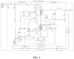
- FIG. 4 is a detailed schematic structural diagram of a power supply guarantee system according to another embodiment of this application.
- the reference numerals used in FIG. 4 to denote structures are the same as the reference numerals used in FIG. 3 for the same or equivalent structures. It needs to be noted that the embodiments are not intended to limit the scope of the disclosure of this application.
- the first rectification and filtering unit includes a first diode network D1 and a third capacitor network C3.
- An input end of the first diode network D1 is connected to a homonymous end of the secondary side coil Ns 1 of the first transformer T1.
- An output end of the first diode network D 1 is connected to one end of the third capacitor network C3.
- the other end of the third capacitor network C3 is connected to a reference voltage end.
- a heteronymous end of the secondary side coil Ns1 of the first transformer T1 is connected to the reference voltage end.
- the first diode network serves a function of rectification, and improves a current passing capacity.
- the third capacitor network serves a function of filtering.
- the first rectifier diode network D1 may include a single diode device, and the third capacitor network C3 may include a single capacitor.
- the first rectifier diode network D1 may also include two or more diodes connected in series and/or in parallel, and the third capacitor network C3 may also include two or more capacitors connected in series and/or in parallel.
- the combination form of the first diode network D1 and the combination form of the third capacitor network C3 may be set according to actual situations in actual application scenarios of power supply guarantee.
- the power conversion module includes a second rectification and filtering unit.
- the second rectification and filtering unit is connected to an output end of the second high voltage transmission module.
- the second rectification and filtering unit is configured to perform rectification and filtering on the synchronously rectified low voltage electrical energy, and transmit the rectified and filtered low voltage electrical energy to the BMS.
- the second rectification and filtering unit may include a second inductor network L2 and a fourth capacitor network C4.
- One end of the second inductor network L2 is connected to the homonymous end of the secondary side coil Ns2 of the second transformer T2.
- the other end of the second inductor network L2 is connected to one end of the fourth capacitor network C4.
- the other end of the fourth capacitor network C4 is connected to the reference voltage end.
- the second inductor network L2 serves functions of isolating alternating current signals and filtering
- the fourth capacitor network C4 serves functions of filtering and voltage regulation.
- the second inductor network L2 may include a single inductor, and the fourth capacitor network C4 may include a single capacitor.
- the second inductor network L2 may also include two or more inductors connected in series and/or in parallel, and the fourth capacitor network C4 may also include two or more capacitors connected in parallel.
- the combination form and the resistance value of the second inductor network L2, and the combination form and the resistance value of the fourth capacitor network C4 may be set according to actual situations in actual application scenarios of power supply guarantee.
- the power supply guarantee system further includes a low-dropout linear regulator module 60 and a first isolation device 70.
- the low-dropout linear regulator module 60 is configured to perform voltage step-down on the low voltage electrical energy to obtain stepped-down electrical energy.
- the main control module 40 is further configured to start working according to the stepped-down electrical energy, and send the wake-up time to the timing device 30 through the first isolation device 70.
- the stepped-down electrical energy provides a working voltage to the main control module so that the main control module starts working.
- the first isolation device serves a function of electrical isolation. The electrical isolation avoids or reduces direct connection between the main control module at the low voltage side and the timing device at the high voltage side, thereby reducing electrical interference and improving safety of the power supply guarantee system.
- the power conversion module further includes a second isolation device 54.
- the second isolation device 54 is configured to electrically isolate a frequency synchronization signal output by the forward power control module 51, and transmit the electrically isolated frequency synchronization signal to the synchronous rectification module 52.
- the synchronous rectification module 52 includes a synchronous rectification power supply end VCC3, a first synchronous rectification output port OUT2, and a second synchronous rectification output port OUT3.
- the second high voltage transmission module includes a second transformer T2, a fourth switch device Q4, and a fifth switch device Q5.
- the first synchronous rectification output port OUT2 is connected to a control end of the fourth switch device.
- a first load access end of the fourth switch device Q4 is connected to a heteronymous end of a secondary side coil Ns2 of the second transformer T2.
- a second load access end of the fourth switch device Q4 is connected to a reference voltage end.
- the second synchronous rectification output port OUT3 is connected to a control end of the fifth switch device Q5.
- a first load access end of the fifth switch device Q5 is connected to a homonymous end of the secondary side coil Ns2 of the second transformer T2.
- a second load access end of the fifth switch device Q5 is connected to the reference voltage end.
- the synchronous rectification module 52 is further configured to receive the electrically isolated frequency synchronization signal output by the second isolation device 54, synchronously control the fourth switch device Q4 and the fifth switch device Q5 to turn on according to the frequency synchronization signal, and transmit low voltage electrical energy to the BMS through the fourth switch device Q4 and the fifth switch device Q5 that are turned on.
- a first frequency synchronization interface SYNC1 of the forward power control module 51 is connected to the second isolation input end IN3 of the second isolation device 54.
- a second drive signal output port OUTS of the second isolation device 54 is connected to a second frequency synchronization interface SYNC2 of a synchronous rectification chip.
- the second isolation device 54 transmits the frequency synchronization signal output by the forward power supply control module, to the synchronous rectification module to achieve signal frequency synchronization between the forward power control module and the synchronous rectification module.
- the VCU delivers a timed wake-up instruction to the BMS, and is then powered off.
- the BMS transmits the timed wake-up instruction to the timing device through the main control module.
- the timing device sets a wake-up time according to the timed wake-up instruction, and then the entire BMS enters a sleep state.
- the timing device delivers a discharge command to the high voltage battery pack.
- the power conversion module converts electrical energy in the high voltage battery pack into low voltage electrical energy for powering the BMS, thereby ensuring normal operation of the BMS.
- the high voltage battery pack outputs a stable 24 V power supply to the low voltage side.
- the power supply is converted by the low-dropout linear regulator module as a power supply to the main control module.
- the low-dropout linear regulator module works normally, the main control module works normally, and the power conversion module works normally, so that the entire BMS works normally.
- the BMS monitors relevant data in the battery, stores the data, and performs corresponding operations. After the foregoing work is completed, if the VCU is not working, the BMS delivers the timed wake-up instruction to the timer and then enters a sleep state again to wait for next timed wake-up.
- the power supply guarantee system if the integrated vehicle contains no lead-acid battery, when the BMS is in the sleep state, the BMS is woken up by the timing device, and a stable power source is provided to the BMS. This ensures that the BMS is in a powered state, facilitates the BMS to collect and store the relevant information in the battery pack of the integrated vehicle, and enables the BMS to monitor the integrated vehicle in real time.
- the power supply guarantee system according to this embodiment of this application wakes up the BMS through the timing device, without resorting to the vehicle lead-acid battery, thereby reducing the loss of lead acid and increasing the life of the lead acid.
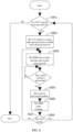
- FIG. 5 is a flowchart of a power supply guarantee method according to an embodiment of this application.
- the power supply guarantee method exemplified in this application is applicable to the power supply guarantee system described in the foregoing embodiments with reference to FIG. 1 to FIG. 4 .
- the power supply guarantee method 500 according to an embodiment of this application includes the following steps.
- Step S510 A main control module receives a wake-up time and sends the received wake-up time to a timing device.
- Step S520 A high voltage power module provides a constant power supply to the timing device according to electrical energy in a high voltage battery pack.
- Step S530 The timing device sets a wake-up clock according to the wake-up time, starts timing when a BMS enters sleep, and sends a discharge instruction to the high voltage battery pack when the timing of the timing device reaches the wake-up time.
- Step S540 A power conversion module converts high voltage electrical energy into low voltage electrical energy, and uses the low voltage electrical energy to power the BMS, where the high voltage electrical energy is output by the high voltage battery pack according to the discharge instruction.
- the wake-up time received by the main control module is a wake-up time that is set by the VCU.
- the main control module may be used to receive the set wake-up time, and send the wake-up time to the timing device.
- the power supply guarantee method may further include the following step: Step S550: Power off the VCU after the wake-up time is set by the VCU, and power off the BMS after the wake-up time is sent to the timing device by the main control module.
- the power supply guarantee method may further include the following step: Step S560: The VCU provides a working voltage to the high voltage battery pack when the timing of the timing device does not reach the wake-up time and the VCU is in a working state, so that the high voltage battery pack starts working.
- the power supply guarantee method may further include the following step: Step S570: The timing device resets the wake-up clock according to the wake-up time when the timing of the timing device reaches the wake-up time and the VCU is in a sleep state.
- the BMS wakes up from the sleep state. If the VCU is not working, the timer continues timing. Once the BMS is woken up from sleep, if the VCU is still not working, the BMS will transmit the timed wake-up instruction to the timer and then enter the sleep state to wait for the next timed wake-up. Once the VCU is found to start working, the sleep state prior to wake-up will end.
- FIG. 6 is a schematic flowchart of a power supply guarantee method according to another embodiment of this application. As shown in FIG. 6 , in an embodiment, the power supply guarantee method may include the following steps.
- step S601 when working normally, the VCU determines whether the VCU needs to be powered off.
- step S602 if the VCU needs to be powered off, the VCU is powered off after delivering a timed wake-up instruction to the BMS. If the VCU does not need to be powered off, the VCU works normally, and the power supply guarantee method process is ended.
- the BMS transmits the timed wake-up instruction to the timing device.
- the timing device sets a wake-up clock according to the wake-up time, and the BMS is powered off and is in a sleep state.
- step S604 when the timing of the timing device reaches a preset wake-up time, the power conversion module is activated by the timing device to start working.
- the step of the timing device activating the power conversion module to start working may specifically include: when the timing of the timer reaches the preset wake-up time, an enable signal is sent to the forward power control module; under the control of the enable signal, the forward power control module starts working; the forward power control module controls an on/off state of the switch device Q1, and controls storage and discharge of electrical energy in a primary side winding Np 1 of the transformer T1 by turning on and turning off the switch device Q1; the forward power control module also controls the on/off state of the switch device Q2 and the switch device Q3; when the switch device Q3 is turned on, the transformer T2 converts high voltage electrical energy into low voltage electrical energy, where the high voltage electrical energy is output by the high voltage battery pack.
- step S605 the high voltage electrical energy of the high voltage battery pack is converted into stable low voltage electrical energy by the power conversion module, and the BMS works normally.
- step S606 it is determined whether the VCU is working normally. If the VCU is working normally, the BMS will not enter the sleep state any longer after completing the normal work.
- step S607 if the VCU is not working normally, that is, if the VCU is still in the sleep state, the timing device resets a wake-up clock according to the wake-up time after the BMS completes normal work, and the BMS is powered off again and is in a sleep state.
- the BMS when the BMS is in the sleep state, the BMS is woken up by the timing device, and a stable power source is provided to the BMS by using the high voltage battery pack. This ensures that the BMS is in a powered state, and enables the BMS to monitor the integrated vehicle in real time.
- an embodiment of this application includes a computer program product.
- the computer program product includes a computer program tangibly contained in a machine-readable medium.
- the computer program includes program code for executing the method shown in the flowchart.
- the computer program may be downloaded and installed from the Internet, and/or installed from a detachable storage medium.
- the foregoing embodiments may be implemented fully or partially by software, hardware, firmware, or any combination thereof.
- the embodiment When implemented by software, the embodiment may be fully or partially implemented in the form of a computer program product.
- the computer program product includes one or more computer instructions.
- the computer instructions When being run on a computer, the computer instructions cause the computer to execute the method described in each embodiment described above.
- the computer program instructions When the computer program instructions are loaded and executed on the computer, the processes or functions described in the embodiments of this application are generated in full or in part.
- the computer may be a general-purpose computer, a dedicated computer, a computer network, or other programmable devices.
- the computer instructions may be stored in a computer-readable storage medium or transmitted from one computer-readable storage medium to another.
- the computer instructions may be transmitted from a website, computer, server, or data center to another website, computer, server, or data center in a wired (such as a coaxial cable, optical fiber, or digital subscriber line (DSL)) or wireless (such as infrared, radio, or microwave) manner.
- the computer-readable storage medium may be any available medium accessible to a computer, or a data storage device such as a server or data center that integrates one or more available medium(s).
- the available medium may be a magnetic medium (such as a floppy disk, a hard disk, or a magnetic tape), an optical medium (such as a DVD), or a semiconductor medium (such as a solid state disk).
- the described apparatus embodiments are merely exemplary.
- the units described as separate parts may or may not be physically separate, and parts displayed as units may or may not be physical units, may be located in one position, and may be distributed on a plurality of network elements.
- a part of or all of the modules may be selected according to the actual needs to achieve the objectives of the solutions of the embodiments.
- a person of ordinary skill in the art can understand and implement the solutions without making any creative efforts.
Landscapes
- Engineering & Computer Science (AREA)
- Power Engineering (AREA)
- Theoretical Computer Science (AREA)
- Transportation (AREA)
- Mechanical Engineering (AREA)
- Life Sciences & Earth Sciences (AREA)
- Sustainable Development (AREA)
- Sustainable Energy (AREA)
- General Engineering & Computer Science (AREA)
- Physics & Mathematics (AREA)
- General Physics & Mathematics (AREA)
- Computer Hardware Design (AREA)
- Microelectronics & Electronic Packaging (AREA)
- Manufacturing & Machinery (AREA)
- Chemical & Material Sciences (AREA)
- Chemical Kinetics & Catalysis (AREA)
- Electrochemistry (AREA)
- General Chemical & Material Sciences (AREA)
- Human Computer Interaction (AREA)
- Charge And Discharge Circuits For Batteries Or The Like (AREA)
- Secondary Cells (AREA)
Description
- This application relates to the field of battery management, and in particular, to a power supply guarantee system and a power supply guarantee method.
- Currently, energy shortage and environmental pollution are increasingly severer, and development of new-energy battery electric vehicles is crucial to reduction of vehicle tail gas and energy consumption as well as mitigation of environmental pressure. A battery management system (BMS) is an important integral part of energy management of a new energy vehicle and implements intelligent management and maintenance for a power battery system of the electric vehicles.
- Generally, a vehicle lead-acid battery provides a power supply for the BMS, and is connected to a low-voltage controller through a power supply bus to power the low-voltage controller. In a conventional power supply system, once the lead-acid battery is absent in the electric vehicle and the BMS is in a sleep state, the BMS will not work normally.
-
CN 108 215 915 A discloses an electric energy transmission circuit and device. The electric energy transmission circuit comprises a wake-up sub-circuit, a high-voltage control sub-circuit and a power conversion sub-circuit. -
CN 106026712 A discloses a switching power supply, especially a secondary-side control method and a secondary-side control circuit of an isolated switching power supply. - An embodiment of this application provides a power supply guarantee system and a power supply guarantee method to keep providing a power supply to a BMS when the BMS is in a sleep state, so that the BMS is always in a powered state and normal operation of the BMS is ensured.
- According to a first aspect of embodiments of this application, a power supply guarantee system is provided, and applied to a BMS. The power supply guarantee system of the invention comprises the features recited in
independent claim 1. - Preferred features of the power supply guarantee system according to the invention are defined in the dependent claims numbered 2 to 13.
- According to another aspect of the embodiments of this application, a power supply guarantee method is provided, and applied to the power supply guarantee system described above, and the power supply guarantee method comprises the steps recited in claim 14.
- With the power supply guarantee system and the power supply guarantee method according to the embodiments of this application, when the BMS is in a sleep state, the BMS is periodically woken up to ensure that the BMS is in a powered state, and to facilitate the BMS to collect and store relevant information in the battery pack of an integrated vehicle. With the power supply guarantee system and the power supply guarantee method according to the embodiments of this application, the BMS is woken up without resorting to a vehicle lead-acid battery, thereby reducing the loss of lead acid and increasing the life of the lead acid.
- To describe technical solutions in embodiments of this application more clearly, the following outlines accompanying drawings used in the embodiments of this application.
-
FIG. 1 is a schematic structural diagram of a system in which a BMS is powered by a vehicle lead-acid battery according to an embodiment of this application; -
FIG. 2 is a schematic structural diagram of a power supply guarantee system according to an embodiment of this application; -
FIG. 3 is a detailed schematic structural diagram of a power supply guarantee system according to another embodiment of this application; -
FIG. 4 is a detailed schematic structural diagram of a power supply guarantee system according to still another embodiment of this application; -
FIG. 5 is a schematic flowchart of a power supply guarantee method according to an embodiment of this application; and -
FIG. 6 is a schematic flowchart of a power supply guarantee method according to another embodiment of this application. - The following describes features and exemplary embodiments of each aspect of this application in detail. To make the objectives, technical solutions, and advantages of this application clearer, the following describes this application in further detail with reference to accompanying drawings and embodiments. For a person skilled in the art, this application may be implemented without some of the specific details. The following description of the embodiments is only intended to enable a better understanding of this application by illustrating examples of this application.
- It needs to be noted that the relational terms herein such as first and second are used only to differentiate an entity or operation from another entity or operation, but do not require or imply any actual relationship or sequence between the entities or operations. Moreover, the terms "include", "comprise", and any variation thereof are intended to cover such a non-exclusive inclusion that a process, method, object, or device that includes or comprises a series of elements not only includes such elements, but also includes other elements not specified expressly or includes inherent elements of the process, method, object, or device. Unless otherwise specified in the context, reference to a process, method, object, or device that "includes" or "comprises" a specific number of elements does not exclude other equivalent elements existent in the process, method, object, or device.
-
FIG. 1 is a schematic structural diagram of a system in which a BMS is powered by a vehicle lead-acid battery according to an embodiment of this application. As shown inFIG. 1 , the vehicle lead-acid battery 101 may power aBMS 102. The BMS 102 may include a battery management unit (BMU) 1021, a DC-DC conversion module 1022, and abattery pack 1023. The DC-DC conversion module 1022 can perform voltage conversion, for example, convert a 24 V system power supply into a 12 V supply to power 12 V-enabled electrical devices in a vehicle. - In a new energy vehicle, the vehicle lead-
acid battery 101 may provide a power supply to theBMS 102, and may also be connected to a low voltage control unit through a power supply bus to power the low voltage control unit. TheBMS 102 exchanges information with a vehicle control unit (VCU) 103 through a controller area network (CAN) bus, and uploads relevant information such as a state of charge (SOC), voltage, and current of thebattery pack 1023 to the VCU. - When an integrated vehicle contains no lead-acid battery and the new energy vehicle is parked for a long time without being used, the VCU and the BMS are powered off. Without being powered by the lead-acid battery, the entire BMS is in a sleep state and unable to monitor the states such as SOC, voltage, and current of the battery pack in the integrated vehicle or to perform corresponding operations.
- Therefore, an embodiment of this application provides a power supply guarantee system and a power supply guarantee method to provide a power source to the BMS. When the BMS is in a sleep state, the BMS is periodically woken up to ensure that the BMS is in a powered state, and to facilitate the BMS to collect and store relevant information in the battery pack of the integrated vehicle. With the power supply guarantee system and the power supply guarantee method according to the embodiments of this application, the BMS is woken up without resorting to a vehicle lead-acid battery, thereby reducing the loss of lead acid and increasing the life of the lead acid.
- To enable better understanding of this application, the following describes in detail the power supply guarantee system and the power supply guarantee method according to an embodiment of this application with reference to accompanying drawings. It needs to be noted that the embodiments are not intended to limit the scope of the disclosure of this application.
-
FIG. 2 is a schematic structural diagram of a power supply guarantee system according to an embodiment of this application. As shown inFIG. 2 , a power supply guarantee system 200 in this embodiment of this application may include: a highvoltage battery pack 10, a highvoltage power module 20, atiming device 30, amain control module 40, and apower conversion module 50. - The
main control module 40 may be configured to send a received wake-up time to the timing device. The highvoltage power module 20 is configured to power thetiming device 30 according to electrical energy in the highvoltage battery pack 10. Thetiming device 30 may be configured to set a wake-up clock according to the wake-up time, start timing when the BMS enters sleep, and send a discharge instruction to the highvoltage battery pack 10 when the timing reaches the wake-up time. Thepower conversion module 50 is configured to convert high voltage electrical energy into low voltage electrical energy, and use the low voltage electrical energy to power the BMS, where the high voltage electrical energy is output by the highvoltage battery pack 10 according to the discharge instruction. - In an embodiment, the wake-up time received by the timing device is a wake-up time that is set by the VCU. In other words, the VCU (not shown in
FIG. 2 ) may be configured to set a wake-up time, and send the wake-up time to the timing device through the main control module. In this embodiment, the main control module may be, for example, a microprogrammed control unit (microprogrammed control unit, MCU). - With the power supply guarantee system according to this embodiment of this application, when the integrated vehicle contains no lead-acid battery and the BMS enters a sleep mode, the power supply can still be provided to the BMS, so that the BMS is always in a powered state and the entire BMS system keeps operating normally.
-
FIG. 3 is a detailed schematic structural diagram of a power supply guarantee system according to another embodiment of this application. The reference numerals used inFIG. 3 to denote structures are the same as the reference numerals used inFIG. 2 for the same or equivalent structures. It needs to be noted that the embodiments are not intended to limit the scope of the disclosure of this application. - As shown in
FIG. 3 , in a power supply guarantee system 200 in an embodiment, thepower conversion module 50 may specifically include: a forwardpower control module 51, a first high voltage transmission module, asynchronous rectification module 52, a first isolation anddriving module 53, and a second high voltage transmission module. - In this embodiment, the
timing device 30 is further configured to provide an enable signal to the forwardpower control module 51 when the timing reaches the wake-up time. The forwardpower control module 51 starts working under the control of enable signal. - The forward
power control module 51 is configured to provide a power supply to thesynchronous rectification module 52 through the first high voltage transmission module, and control an on-state of connection between the highvoltage battery pack 10 and the second high voltage transmission module through the first isolation anddriving module 53. - The second high voltage transmission module is configured to convert high voltage electrical energy in the high
voltage battery pack 10 into low voltage electrical energy when the connection between the second high voltage transmission module and the highvoltage battery pack 10 is turned on. - The
synchronous rectification module 52 is configured to perform synchronous rectification on the low voltage electrical energy, and use the synchronously rectified low voltage electrical energy to power the BMS. - In this embodiment of this application, when the integrated vehicle needs to be powered off, the VCU can set the wake-up time in advance, generate a timed wake-up instruction according to the wake-up time, and deliver the wake-up instruction to the BMS, and then the VCU is powered off. The BMS delivers the timed wake-up instruction to the timing device through the main control module. After a timer sets a time, the entire BMS will enter a sleep state. When the timing of the timing device reaches the wake-up time, the timing device delivers a discharge command to the high voltage battery pack. The power conversion module converts electrical energy in the high voltage battery pack into low voltage electrical energy as a power source to the BMS, so that the BMS is woken up from sleep, and starts to monitor relevant information such as the SOC, voltage, and current in the battery pack of the integrated vehicle and perform corresponding operations.
- Still referring to
FIG. 3 , in an embodiment, the high voltage power module includes a first power access point B, a first voltage divider resistor network R1, a second voltage divider resistor network R2, and a first voltage regulator unit DZ1. Thetiming device 30 includes a clock power supply end VCC1. - In an embodiment, the first power access point B is located at a positive electrode of the high
voltage battery pack 10. One end of the first voltage divider resistor network R1 is connected to the first power access point B. The other end of the first voltage divider resistor network R1 is connected to one end of the second voltage divider resistor network R2. The other end of the second voltage divider resistor network R2 is connected to the clock power supply end VCC1. One end of the first voltage regulator unit DZ1 is connected to the clock power supply end VCC1. The other end of the first voltage regulator unit DZ1 is connected to a reference voltage end. - In an embodiment, the first voltage divider resistor network R1 and the second voltage divider resistor network R2 may each include a plurality of serial-connected resistors, and the first voltage regulator unit DZ1 may include a Zener diode.
- In this embodiment, the first power access point B provides a constant power supply VRTC to the timing device through the first voltage divider resistor network R1 and the second voltage divider resistor network R2. The first voltage regulator unit DZ1 regulates the constant power supply so that the clock power supply end VCC1 of the
timing device 30 obtains a stable working voltage. - Still referring to
FIG. 3 , the power conversion module includes a resonant filter module. An input end of the resonant filter module is connected to the high voltage battery pack, and an output end of the resonant filter module is connected to the high voltage power module. - In an embodiment, the resonant filter module includes a first capacitor network C1, a second capacitor network C2, and a first inductor network L1.
- One end of the first capacitor network C1 is connected to the high
voltage battery pack 10. The other end of the first capacitor network C1 is connected to a reference voltage end. One end of the first inductor network L1 is connected to the highvoltage battery pack 10. The other end of the first inductor network L1 is connected to one end of the second capacitor network C2. The other end of the second capacitor network C2 is connected to the reference voltage end. - In this embodiment, through series resonance of a capacitor and an inductor, the resonant filter module filters out a harmonic current whose frequency is identical or similar to this resonant frequency in the circuit. This prevents a large quantity of harmonics from flowing into the capacitor and causing damage to the capacitor, and enhances safety of the power supply guarantee system.
- As shown in
FIG. 3 , in an embodiment, thetiming device 30 may include a real-time clock (RTC), a clock power supply end VCC1, a clock input end IN1, and a clock output end OUT 1. - The
timing device 30 is further configured to receive the wake-up time through the clock input end IN1, and set the RTC according to the wake-up time, cause the RTC to start timing when the BMS enters sleep, and output an enable signal through the clock output end OUT1 when the timing reaches the wake-up time. - In an embodiment, the high
voltage power module 20 includes a first power access point B, a first voltage divider resistor network R1, and a second voltage regulator unit DZ2. The forwardpower control module 51 includes an enable end and a forward power supply end VCC2. - The first power access point B is located at a positive electrode of the high
voltage battery pack 10. One end of the first voltage divider resistor network R1 is connected to the first power access point B. The other end of the first voltage divider resistor network R1 is connected to the forward power supply end VCC2. - In addition, the high
voltage power module 20 is further configured to use electrical energy in the highvoltage battery pack 10 to provide a working voltage to the forwardpower control module 51 through the first power access point B and the second voltage divider resistor network R2. - The forward
power control module 51 is further configured to receive the enable signal through the enable end, and use the enable signal to cause the forwardpower control module 51 to start working. - In this embodiment, the first power access point B provides a constant power supply VAUX to the forward
power control module 51 through the first voltage divider resistor network R1. The second voltage regulator unit DZ2 regulates the constant power supply so that the forward power supply end VCC2 of the forwardpower control module 51 obtains a stable starting voltage. - In this embodiment, the second voltage divider resistor network R2 serves a function of voltage division. Through adjustment of a resistance of the second voltage divider resistor network R2, a variation range of the working voltage of the forward power control module can be adjusted, so that the forward power control module obtains a stable working voltage.
- In the power supply guarantee system shown in
FIG. 3 , the first voltage divider resistor network R1 and the second voltage divider resistor network R2 each include one resistor. In other embodiments, the first voltage divider resistor network R1 and the second voltage divider resistor network R2 may each include two or more resistors connected in series and/or in parallel. - It needs to be noted that the combination form and the resistance value of the first voltage divider resistor network R1, and the combination form and the resistance value of the second voltage divider resistor network R2, may be set according to actual situations in actual application scenarios of the power supply guarantee system.
- As shown in
FIG. 3 , in an embodiment, the first high voltage transmission module includes a first switch device Q1 and a first transformer T1, and the forwardpower control module 51 includes a first control signal output port GATE2. The forwardpower control module 51 is further configured to control an on/off state of the first switch device Q1 through the first control signal output port GATE2. - When the first switch device Q1 is turned on, a first part Np1 of a primary side coil of the first transformer T1 stores energy. When the first switch device Q1 is turned off, the energy stored in the first part Np1 of the primary side coil is coupled to a second part Np2 of the primary side coil and a secondary side coil Ns1 of the first transformer T1.
- When the first switch device Q1 is turned off, a power supply is provided to the
synchronous rectification module 52 by using the electrical energy coupled to the secondary side coil Ns1 of the first transformer T1, and electrical energy is provided to the forwardpower control module 51 by using the electrical energy coupled to the second part Np2 of the primary side coil of the first transformer. - Still referring to
FIG. 3 , thepower conversion module 50 further includes a first rectification and filtering unit. The first rectification and filtering unit is connected to the synchronous rectification power supply end VCC3 of thesynchronous rectification module 52. - The first rectification and filtering unit is configured to perform rectification and filtering on the electrical energy coupled to the secondary side coil Ns1 of the first transformer T1, and input the rectified and filtered electrical energy into the synchronous rectification power supply end VCC3.
- In this embodiment of this application, when the RTC of the
timing device 30 reaches the set time (that is, reaches the wake-up time), the clock output end OUT1 of thetiming device 30 enables the forwardpower control module 51 such as an enable pin of a forward control chip. In this case, the first transformer T1 starts to work, and outputs electrical energy at a high voltage side to power the forwardpower control module 51 at the same time. - As shown in
FIG. 3 , in an embodiment, the forwardpower control module 51 includes a second control signal output port GATE1 and a third control signal output port HOUT. The first isolation and drivingmodule 53 includes a first isolation input end IN2 and a first drive signal output port OUT4. The second high voltage transmission module includes a second switch device Q2 and a third switch device Q3. - The forward
power control module 51 is further configured to control an on-state of the second switch device Q2 through a second control signal output by the second control signal output port GATE1, output a third control signal through the third control signal output port HOUT, and transmit the third control signal to the first isolation input end IN2. - The first isolation and driving
module 53 is configured to output a first drive signal through the first drive signal output port OUT4 according to the second control signal received by the first isolation input end IN2, so as to control an on-state of the third switch device Q3. - The forward
power control module 51 is further configured to control the connection between the high voltage battery pack and the second high voltage transmission module to turn on when the second switch device Q2 is turned on and the third switch device Q3 is turned on. - In this embodiment, the high voltage electrical energy in the high voltage battery pack is transmitted to the low voltage side of the second transformer T2 through the second switch device Q2 and the third switch device Q3 that are turned on, and the second transformer T2 outputs low voltage electrical energy.
-
FIG. 4 is a detailed schematic structural diagram of a power supply guarantee system according to another embodiment of this application. The reference numerals used inFIG. 4 to denote structures are the same as the reference numerals used inFIG. 3 for the same or equivalent structures. It needs to be noted that the embodiments are not intended to limit the scope of the disclosure of this application. - As shown in
FIG. 4 , in an embodiment, the first rectification and filtering unit includes a first diode network D1 and a third capacitor network C3. An input end of the first diode network D1 is connected to a homonymous end of the secondary side coil Ns 1 of the first transformer T1. An output end of the firstdiode network D 1 is connected to one end of the third capacitor network C3. The other end of the third capacitor network C3 is connected to a reference voltage end. A heteronymous end of the secondary side coil Ns1 of the first transformer T1 is connected to the reference voltage end. - In the power supply guarantee system shown in
FIG. 3 , the first diode network serves a function of rectification, and improves a current passing capacity. The third capacitor network serves a function of filtering. - In an embodiment, the first rectifier diode network D1 may include a single diode device, and the third capacitor network C3 may include a single capacitor. In other embodiments, the first rectifier diode network D1 may also include two or more diodes connected in series and/or in parallel, and the third capacitor network C3 may also include two or more capacitors connected in series and/or in parallel.
- It needs to be noted that the combination form of the first diode network D1 and the combination form of the third capacitor network C3 may be set according to actual situations in actual application scenarios of power supply guarantee.
- In an embodiment, the power conversion module includes a second rectification and filtering unit. The second rectification and filtering unit is connected to an output end of the second high voltage transmission module.
- The second rectification and filtering unit is configured to perform rectification and filtering on the synchronously rectified low voltage electrical energy, and transmit the rectified and filtered low voltage electrical energy to the BMS.
- In an embodiment, the second rectification and filtering unit may include a second inductor network L2 and a fourth capacitor network C4.
- One end of the second inductor network L2 is connected to the homonymous end of the secondary side coil Ns2 of the second transformer T2. The other end of the second inductor network L2 is connected to one end of the fourth capacitor network C4. The other end of the fourth capacitor network C4 is connected to the reference voltage end.
- In the power supply guarantee system shown in
FIG. 4 , the second inductor network L2 serves functions of isolating alternating current signals and filtering, and the fourth capacitor network C4 serves functions of filtering and voltage regulation. - In an embodiment, the second inductor network L2 may include a single inductor, and the fourth capacitor network C4 may include a single capacitor. In other embodiments, the second inductor network L2 may also include two or more inductors connected in series and/or in parallel, and the fourth capacitor network C4 may also include two or more capacitors connected in parallel.
- It needs to be noted that the combination form and the resistance value of the second inductor network L2, and the combination form and the resistance value of the fourth capacitor network C4, may be set according to actual situations in actual application scenarios of power supply guarantee.
- As shown in
FIG. 4 , in an embodiment, the power supply guarantee system further includes a low-dropout linear regulator module 60 and a first isolation device 70. - The low-dropout linear regulator module 60 is configured to perform voltage step-down on the low voltage electrical energy to obtain stepped-down electrical energy. The
main control module 40 is further configured to start working according to the stepped-down electrical energy, and send the wake-up time to thetiming device 30 through the first isolation device 70. - In this embodiment, the stepped-down electrical energy provides a working voltage to the main control module so that the main control module starts working. The first isolation device serves a function of electrical isolation. The electrical isolation avoids or reduces direct connection between the main control module at the low voltage side and the timing device at the high voltage side, thereby reducing electrical interference and improving safety of the power supply guarantee system.
- As shown in
FIG. 4 , in an embodiment, the power conversion module further includes a second isolation device 54. The second isolation device 54 is configured to electrically isolate a frequency synchronization signal output by the forwardpower control module 51, and transmit the electrically isolated frequency synchronization signal to thesynchronous rectification module 52. - As shown in
FIG. 4 , in an embodiment, thesynchronous rectification module 52 includes a synchronous rectification power supply end VCC3, a first synchronous rectification output port OUT2, and a second synchronous rectification output port OUT3. The second high voltage transmission module includes a second transformer T2, a fourth switch device Q4, and a fifth switch device Q5. - The first synchronous rectification output port OUT2 is connected to a control end of the fourth switch device. A first load access end of the fourth switch device Q4 is connected to a heteronymous end of a secondary side coil Ns2 of the second transformer T2. A second load access end of the fourth switch device Q4 is connected to a reference voltage end.
- The second synchronous rectification output port OUT3 is connected to a control end of the fifth switch device Q5. A first load access end of the fifth switch device Q5 is connected to a homonymous end of the secondary side coil Ns2 of the second transformer T2. A second load access end of the fifth switch device Q5 is connected to the reference voltage end.
- The
synchronous rectification module 52 is further configured to receive the electrically isolated frequency synchronization signal output by the second isolation device 54, synchronously control the fourth switch device Q4 and the fifth switch device Q5 to turn on according to the frequency synchronization signal, and transmit low voltage electrical energy to the BMS through the fourth switch device Q4 and the fifth switch device Q5 that are turned on. - In an embodiment, a first frequency synchronization interface SYNC1 of the forward
power control module 51 is connected to the second isolation input end IN3 of the second isolation device 54. A second drive signal output port OUTS of the second isolation device 54 is connected to a second frequency synchronization interface SYNC2 of a synchronous rectification chip. - In this embodiment, the second isolation device 54 transmits the frequency synchronization signal output by the forward power supply control module, to the synchronous rectification module to achieve signal frequency synchronization between the forward power control module and the synchronous rectification module.
- With the power supply guarantee system according to this embodiment of this application, the VCU delivers a timed wake-up instruction to the BMS, and is then powered off. After receiving the timed wake-up instruction, the BMS transmits the timed wake-up instruction to the timing device through the main control module. The timing device sets a wake-up time according to the timed wake-up instruction, and then the entire BMS enters a sleep state. When the timing of the timing device reaches the wake-up time, the timing device delivers a discharge command to the high voltage battery pack. The power conversion module converts electrical energy in the high voltage battery pack into low voltage electrical energy for powering the BMS, thereby ensuring normal operation of the BMS.
- In the power supply guarantee system according to this embodiment of this application, the high voltage battery pack outputs a stable 24 V power supply to the low voltage side. The power supply is converted by the low-dropout linear regulator module as a power supply to the main control module. In this way, the low-dropout linear regulator module works normally, the main control module works normally, and the power conversion module works normally, so that the entire BMS works normally. Subsequently, the BMS monitors relevant data in the battery, stores the data, and performs corresponding operations. After the foregoing work is completed, if the VCU is not working, the BMS delivers the timed wake-up instruction to the timer and then enters a sleep state again to wait for next timed wake-up.
- With the power supply guarantee system according to this embodiment of this application, if the integrated vehicle contains no lead-acid battery, when the BMS is in the sleep state, the BMS is woken up by the timing device, and a stable power source is provided to the BMS. This ensures that the BMS is in a powered state, facilitates the BMS to collect and store the relevant information in the battery pack of the integrated vehicle, and enables the BMS to monitor the integrated vehicle in real time. The power supply guarantee system according to this embodiment of this application wakes up the BMS through the timing device, without resorting to the vehicle lead-acid battery, thereby reducing the loss of lead acid and increasing the life of the lead acid.
-
FIG. 5 is a flowchart of a power supply guarantee method according to an embodiment of this application. The power supply guarantee method exemplified in this application is applicable to the power supply guarantee system described in the foregoing embodiments with reference toFIG. 1 to FIG. 4 . As shown inFIG. 5 , the powersupply guarantee method 500 according to an embodiment of this application includes the following steps. - Step S510: A main control module receives a wake-up time and sends the received wake-up time to a timing device.
- Step S520: A high voltage power module provides a constant power supply to the timing device according to electrical energy in a high voltage battery pack.
- Step S530: The timing device sets a wake-up clock according to the wake-up time, starts timing when a BMS enters sleep, and sends a discharge instruction to the high voltage battery pack when the timing of the timing device reaches the wake-up time.
- Step S540: A power conversion module converts high voltage electrical energy into low voltage electrical energy, and uses the low voltage electrical energy to power the BMS, where the high voltage electrical energy is output by the high voltage battery pack according to the discharge instruction.
- In an embodiment, the wake-up time received by the main control module is a wake-up time that is set by the VCU. In this embodiment, the main control module may be used to receive the set wake-up time, and send the wake-up time to the timing device.
- In an embodiment, the power supply guarantee method may further include the following step:
Step S550: Power off the VCU after the wake-up time is set by the VCU, and power off the BMS after the wake-up time is sent to the timing device by the main control module. - In an embodiment, the power supply guarantee method may further include the following step:
Step S560: The VCU provides a working voltage to the high voltage battery pack when the timing of the timing device does not reach the wake-up time and the VCU is in a working state, so that the high voltage battery pack starts working. - In an embodiment, the power supply guarantee method may further include the following step:
Step S570: The timing device resets the wake-up clock according to the wake-up time when the timing of the timing device reaches the wake-up time and the VCU is in a sleep state. - In this embodiment of this application, when the VCU starts working during a period of timing by the timer, the BMS wakes up from the sleep state. If the VCU is not working, the timer continues timing. Once the BMS is woken up from sleep, if the VCU is still not working, the BMS will transmit the timed wake-up instruction to the timer and then enter the sleep state to wait for the next timed wake-up. Once the VCU is found to start working, the sleep state prior to wake-up will end.
-
FIG. 6 is a schematic flowchart of a power supply guarantee method according to another embodiment of this application. As shown inFIG. 6 , in an embodiment, the power supply guarantee method may include the following steps. - As shown in step S601, when working normally, the VCU determines whether the VCU needs to be powered off.
- As shown in step S602, if the VCU needs to be powered off, the VCU is powered off after delivering a timed wake-up instruction to the BMS. If the VCU does not need to be powered off, the VCU works normally, and the power supply guarantee method process is ended.
- As shown in step S603, the BMS transmits the timed wake-up instruction to the timing device. The timing device sets a wake-up clock according to the wake-up time, and the BMS is powered off and is in a sleep state.
- As shown in step S604, when the timing of the timing device reaches a preset wake-up time, the power conversion module is activated by the timing device to start working.
- In this step, the step of the timing device activating the power conversion module to start working may specifically include: when the timing of the timer reaches the preset wake-up time, an enable signal is sent to the forward power control module; under the control of the enable signal, the forward power control module starts working; the forward power control module controls an on/off state of the switch device Q1, and controls storage and discharge of electrical energy in a primary
side winding Np 1 of the transformer T1 by turning on and turning off the switch device Q1; the forward power control module also controls the on/off state of the switch device Q2 and the switch device Q3; when the switch device Q3 is turned on, the transformer T2 converts high voltage electrical energy into low voltage electrical energy, where the high voltage electrical energy is output by the high voltage battery pack. - As shown in step S605, the high voltage electrical energy of the high voltage battery pack is converted into stable low voltage electrical energy by the power conversion module, and the BMS works normally.
- As shown in step S606, it is determined whether the VCU is working normally. If the VCU is working normally, the BMS will not enter the sleep state any longer after completing the normal work.
- As shown in step S607, if the VCU is not working normally, that is, if the VCU is still in the sleep state, the timing device resets a wake-up clock according to the wake-up time after the BMS completes normal work, and the BMS is powered off again and is in a sleep state.
- In the power supply guarantee method according to this embodiment of this application, when the BMS is in the sleep state, the BMS is woken up by the timing device, and a stable power source is provided to the BMS by using the high voltage battery pack. This ensures that the BMS is in a powered state, and enables the BMS to monitor the integrated vehicle in real time.
- Evidently, this application is not limited to the specific configuration and processing described in the foregoing embodiments and shown in the drawings. For convenience and brevity of description, detailed descriptions of known methods are omitted herein. The corresponding processes in the method embodiments described above can be learned by referring to the specific working processes of the systems, modules, and units described earlier herein, and are not repeated here again.
- According to the embodiments of this application, the processes described above with reference to the flowchart may be implemented in the form of a computer software program. For example, an embodiment of this application includes a computer program product. The computer program product includes a computer program tangibly contained in a machine-readable medium. The computer program includes program code for executing the method shown in the flowchart. In such an embodiment, the computer program may be downloaded and installed from the Internet, and/or installed from a detachable storage medium.
- The foregoing embodiments may be implemented fully or partially by software, hardware, firmware, or any combination thereof. When implemented by software, the embodiment may be fully or partially implemented in the form of a computer program product. The computer program product includes one or more computer instructions. When being run on a computer, the computer instructions cause the computer to execute the method described in each embodiment described above. When the computer program instructions are loaded and executed on the computer, the processes or functions described in the embodiments of this application are generated in full or in part. The computer may be a general-purpose computer, a dedicated computer, a computer network, or other programmable devices. The computer instructions may be stored in a computer-readable storage medium or transmitted from one computer-readable storage medium to another. For example, the computer instructions may be transmitted from a website, computer, server, or data center to another website, computer, server, or data center in a wired (such as a coaxial cable, optical fiber, or digital subscriber line (DSL)) or wireless (such as infrared, radio, or microwave) manner. The computer-readable storage medium may be any available medium accessible to a computer, or a data storage device such as a server or data center that integrates one or more available medium(s). The available medium may be a magnetic medium (such as a floppy disk, a hard disk, or a magnetic tape), an optical medium (such as a DVD), or a semiconductor medium (such as a solid state disk).
- The described apparatus embodiments are merely exemplary. The units described as separate parts may or may not be physically separate, and parts displayed as units may or may not be physical units, may be located in one position, and may be distributed on a plurality of network elements. A part of or all of the modules may be selected according to the actual needs to achieve the objectives of the solutions of the embodiments. A person of ordinary skill in the art can understand and implement the solutions without making any creative efforts.
Claims (14)
- A power supply guarantee system, applied to a battery management system (102), characterized in that the power supply guarantee system comprises: a main control module (40), a high voltage battery pack (10), a high voltage power module (20), a timing device (30), and a power conversion module (50), whereinthe main control module (40) is configured to send a received wake-up time to the timing device (30);the high voltage power module (20) is configured to power the timing device (30) according to electrical energy in the high voltage battery pack (10);the timing device (30) is configured to set a wake-up clock according to the wake-up time, start timing when the battery management system (102) enters sleep, and send a discharge instruction to the high voltage battery pack (10) when the timing reaches the wake-up time; andthe power conversion module (50) is configured to convert high voltage electrical energy into low voltage electrical energy, and use the low voltage electrical energy to power the battery management system (102), wherein the high voltage electrical energy is output by the high voltage battery pack (10) according to the discharge instruction,wherein the power conversion module (50) comprises: a forward power control module (51), a first high voltage transmission module, a synchronous rectification module (52), a first isolation and driving module (53), and a second high voltage transmission module, wherein the first high voltage transmission module and the second high voltage transmission module are not the same module, whereinthe timing device (30) is further configured to provide an enable signal to the forward power control module (51) when the timing reaches the wake-up time, so that the forward power control module (51) starts working under the control of the enable signal;the forward power control module (51) is configured to provide a power supply to the synchronous rectification module (52) through the first high voltage transmission module; andthe second high voltage transmission module is configured to convert high voltage electrical energy in the high voltage battery pack (10) into low voltage electrical energy when the connection between the second high voltage transmission module and the high voltage battery pack (10) is turned on; andthe synchronous rectification module (52) is configured to perform synchronous rectification on the low voltage electrical energy, and use the synchronously rectified low voltage electrical energy to power the battery management system (102), characterized in that the forward power control module (51) is configured to control an on-state of connection between the high voltage battery pack (10) and the second high voltage transmission module through the first isolation and driving module (53).
- The power supply guarantee system according to claim 1, wherein the high voltage power module (20) comprises a first power access point (B), a first voltage divider resistor network (R1), a second voltage divider resistor network (R2), and a first voltage regulator unit (DZ1), and the timing device (30) comprises a clock power supply end (VCC1), wherein
the first power access point (B) is located at a positive electrode of the high voltage battery pack (10), one end of the first voltage divider resistor network (R1) is connected to the first power access point (B), the other end of the first voltage divider resistor network (R1) is connected to one end of the second voltage divider resistor network (R2), the other end of the second voltage divider resistor network (R2) is connected to the clock power supply end (VCC1), one end of the first voltage regulator unit (DZ1) is connected to the clock power supply end (VCC1), and the other end of the first voltage regulator unit (DZ1) is connected to a reference voltage end. - The power supply guarantee system according to claim 1, wherein the power conversion module (50) comprises a resonant filter module, an input end of the resonant filter module is connected to the high voltage battery pack (10), and an output end of the resonant filter module is connected to the high voltage power module (20).
- The power supply guarantee system according to claim 3, wherein the resonant filter module comprises a first capacitor network (C1), a second capacitor network (C2), and a first inductor network (L1);
one end of the first capacitor network (C1) is connected to the high voltage battery pack (10), the other end of the first capacitor network (C1) is connected to a reference voltage end, one end of the first inductor network (L1) is connected to the high voltage battery pack (10), the other end of the first inductor network (L1) is connected to one end of the second capacitor network (C2), and the other end of the second capacitor network (C2) is connected to the reference voltage end. - The power supply guarantee system according to claim 1, wherein the timing device (30) comprises a real-time clock, a clock power supply end (VCC1), a clock input end (IN1), and a clock output end (OUT1), whereinthe timing device (30) is further configured to receive the wake-up time through the clock input end (IN1), and set the real-time clock according to the wake-up time; andthe real-time clock starts timing when the battery management system (102) enters sleep, and outputs and provides an enable signal through the clock output end (OUT1) when the timing reaches the wake-up time.
- The power supply guarantee system according to claim 1, wherein the high voltage power module (20) comprises a first power access point (B), a first voltage divider resistor network (R1), and a second voltage regulator unit (DZ2), and the forward power control module (51) comprises an enable end (Enable) and a forward power supply end (VCC2), whereinthe first power access point (B) is located at a positive electrode of the high voltage battery pack (10), one end of the first voltage divider resistor network (R1) is connected to the first power access point (B), and the other end of the first voltage divider resistor network (R1) is connected to the forward power supply end (VCC2);the high voltage power module (20) is further configured to use electrical energy in the high voltage battery pack (10) to provide a working voltage to the forward power control module (51) through the first power access point (B), the first voltage divider resistor network (R1), and the second voltage regulator unit (DZ2); andthe forward power control module (51) is further configured to receive the enable signal through the enable end (Enable), and use the enable signal to cause the forward power control module (51) to start working.
- The power supply guarantee system according to claim 1, wherein the first high voltage transmission module comprises a first switch device (Q1) and a first transformer (T1), and the forward power control module (51) comprises a first control signal output port (GATE2), whereinthe forward power control module (51) is further configured to: control an on/off state of the first switch device (Q1) through the first control signal output port (GATE2);when the first switch device (Q1) is turned on, store energy through a first part (Np1) of a primary side coil of the first transformer (T1); when the first switch device (Q1) is turned off, couple the energy stored in the first part (Np1) of the primary side coil to a second part (Np2) of the primary side coil and a secondary side coil (Ns1) of the first transformer (T1);when the first switch device (Q1) is turned off, provide a power supply to the synchronous rectification module (52) by using the electrical energy coupled to the secondary side coil (Ns1) of the first transformer (T1); andprovide electrical energy to the forward power control module (51) by using the electrical energy coupled to the second part (Np2) of the primary side coil of the first transformer (T1).
- The power supply guarantee system according to claim7, wherein the power conversion module (50) further comprises a first rectification and filtering unit, and the first rectification and filtering unit is connected to a synchronous rectification power supply end (VCC3) of the synchronous rectification module (52), wherein
the first rectification and filtering unit is configured to perform rectification and filtering on the electrical energy coupled to the secondary side coil (Ns1) of the first transformer (T1), and input the rectified and filtered electrical energy into the synchronous rectification power supply end (VCC3). - The power supply guarantee system according to claim 8, wherein the first rectification and filtering unit comprises a first diode network (D1) and a third capacitor network (C3), wherein
an input end of the first diode network (D1) is connected to a homonymous end of the secondary side coil (Ns1) of the first transformer (T1), an output end of the first diode network (D1) is connected to one end of the third capacitor network (C3), the other end of the third capacitor network (C3) is connected to a reference voltage end, and a heteronymous end of the secondary side coil (Ns1) of the first transformer (T1) is connected to the reference voltage end. - The power supply guarantee system according to claim 1, wherein the forward power control module (51) comprises a second control signal output port (GATE1) and a third control signal output port (HOUT), the first isolation and driving module (53) comprises a first isolation input end (IN2) and a first drive signal output port (OUT4), and the second high voltage transmission module comprises a second switch device (Q2) and a third switch device (Q3), whereinthe forward power control module (51) is further configured to control an on-state of the second switch device (Q2) through a second control signal output by the second control signal output port (GATE1), output a third control signal through the third control signal output port (HOUT), and transmit the third control signal to the first isolation input end (IN2);the first isolation and driving module (53) is configured to output a first drive signal through the first drive signal output port (OUT4) according to the second control signal received by the first isolation input end (IN2), so as to control an on-state of the third switch device (Q3); andthe forward power control module (51) is further configured to control the connection between the high voltage battery pack (10) and the second high voltage transmission module to turn on when the second switch device (Q2) is turned on and the third switch device (Q3) is turned on.
- The power supply guarantee system according to claim 1, wherein the synchronous rectification module (52) comprises a synchronous rectification power supply end (VCC3), a first synchronous rectification output port (OUT2), and a second synchronous rectification output port (OUT3), and the second high voltage transmission module comprises a second transformer (T2), a fourth switch device (Q4), and a fifth switch device (Q5), whereinthe first synchronous rectification output port (OUT2) is connected to a control end of the fourth switch device (Q4), a first load access end of the fourth switch device (Q4) is connected to a heteronymous end of a secondary side coil (Ns2) of the second transformer (T2), and a second load access end of the fourth switch device (Q4) is connected to a reference voltage end;the second synchronous rectification output port (OUT3) is connected to a control end of the fifth switch device (Q5), a first load access end of the fifth switch device (Q5) is connected to a homonymous end of the secondary side coil (Ns2) of the second transformer (T2), and a second load access end of the fifth switch device (Q5) is connected to the reference voltage end; andthe synchronous rectification module (52) is further configured to: detect low voltage electrical energy output by the second high voltage transmission module; when the low voltage electrical energy meets a low voltage threshold condition, control the fourth switch device (Q4) and the fifth switch device (Q5) to turn on; and transmit the low voltage electrical energy to the battery management system (102) through the fourth switch device (Q4) and the fifth switch device (Q5) that are turned on.
- The power supply guarantee system according to claim 1, wherein the power conversion module (50) comprises a second rectification and filtering unit, and the second rectification and filtering unit is connected to an output end of the second high voltage transmission module, wherein
the second rectification and filtering unit is configured to perform rectification and filtering on the synchronously rectified low voltage electrical energy, and transmit the rectified and filtered low voltage electrical energy to the battery management system (102). - The power supply guarantee system according to claim 11, wherein the power supply guarantee system further comprises a second rectification and filtering unit, and the second rectification and filtering unit comprises a second inductor network (L2) and a fourth capacitor network (C4);
one end of the second inductor network (L2) is connected to the homonymous end of the secondary side coil (Ns2) of the second transformer (T2), the other end of the second inductor network (L2) is connected to one end of the fourth capacitor network (C4), and the other end of the fourth capacitor network (C4) is connected to the reference voltage end. - A power supply guarantee method (500), applicable to the power supply guarantee system according to any of claims 1 to 13, characterized in that the power supply guarantee method comprises:receiving, by a main control module (40), a wake-up time and sending the received wake-up time to a timing device (30) (S510);providing, by a high voltage power module (20), a constant power supply to the timing device (30) according to electrical energy in a high voltage battery pack (10) (S520);setting, by the timing device (30), a wake-up clock according to the wake-up time, starting timing when a battery management system (102) enters sleep, and sending a discharge instruction to the high voltage battery pack (10) when the timing of the timing device (30) reaches the wake-up time (S530); andconverting, by a power conversion module (50), high voltage electrical energy into low voltage electrical energy, and using the low voltage electrical energy to power the battery management system (102), wherein the high voltage electrical energy is output by the high voltage battery pack (10) according to the discharge instruction (S540);wherein the power conversion module (50) comprises: a forward power control module (51), a first high voltage transmission module, a synchronous rectification module (52), a first isolation and driving module (53), and a second high voltage transmission module, wherein the first high voltage transmission module and the second high voltage transmission module are not the same module,wherein the method further comprises:characterized in controlling, by the forward power control module (51), an on-state of connection between the high voltage battery pack (10) and the second high voltage transmission module through the first isolation and driving module (53).providing, by the timing device (30), an enable signal to the forward power control module (51) when the timing reaches the wake-up time, so that the forward power control module (51) starts working under the control of the enable signal;providing, by the forward power control module (51), a power supply to the synchronous rectification module (52) through the first high voltage transmission module;converting, by the second high voltage transmission module, high voltage electrical energy in the high voltage battery pack (10) into low voltage electrical energy when the connection between the second high voltage transmission module and the high voltage battery pack (10) is turned on; andperforming, by the synchronous rectification module (52), synchronous rectification on the low voltage electrical energy, and using, by the synchronous rectification module (52), the synchronously rectified low voltage electrical energy to power the battery management system (102),
Applications Claiming Priority (2)
| Application Number | Priority Date | Filing Date | Title |
|---|---|---|---|
| CN201910641181.9A CN112238788B (en) | 2019-07-16 | 2019-07-16 | Power supply guarantee system and power supply guarantee method |
| PCT/CN2020/099276 WO2021008354A1 (en) | 2019-07-16 | 2020-06-30 | Power supply ensuring system and power supply ensuring method |
Publications (3)
| Publication Number | Publication Date |
|---|---|
| EP3925819A1 EP3925819A1 (en) | 2021-12-22 |
| EP3925819A4 EP3925819A4 (en) | 2022-04-27 |
| EP3925819B1 true EP3925819B1 (en) | 2024-12-04 |
Family
ID=74167015
Family Applications (1)
| Application Number | Title | Priority Date | Filing Date |
|---|---|---|---|
| EP20841021.7A Active EP3925819B1 (en) | 2019-07-16 | 2020-06-30 | Power supply ensuring system and power supply ensuring method |
Country Status (5)
| Country | Link |
|---|---|
| US (1) | US20220121262A1 (en) |
| EP (1) | EP3925819B1 (en) |
| CN (1) | CN112238788B (en) |
| HU (1) | HUE069787T2 (en) |
| WO (1) | WO2021008354A1 (en) |
Families Citing this family (5)
| Publication number | Priority date | Publication date | Assignee | Title |
|---|---|---|---|---|
| CN113895381A (en) * | 2021-10-09 | 2022-01-07 | 浙江吉利控股集团有限公司 | Vehicle power supply circuit, equipment and car |
| US20230400523A1 (en) * | 2022-06-13 | 2023-12-14 | Caterpillar Inc. | System and method for monitoring health parameters of battery pack |
| CN115837860B (en) * | 2022-10-08 | 2024-11-22 | 宁德时代新能源科技股份有限公司 | BMS sleep wake-up circuit, method, BMS and electrical equipment |
| CN115695494A (en) * | 2022-10-31 | 2023-02-03 | 重庆长安汽车股份有限公司 | Vehicle feed risk monitoring method, device, equipment and storage medium |
| CN116766931B (en) * | 2023-06-08 | 2026-01-06 | 深蓝汽车科技有限公司 | Vehicle battery management system, data acquisition methods, equipment and vehicles |
Family Cites Families (15)
| Publication number | Priority date | Publication date | Assignee | Title |
|---|---|---|---|---|
| US7548435B2 (en) * | 2006-03-31 | 2009-06-16 | Astec International Limited | Zero-voltage-switching DC-DC converters with synchronous rectifiers |
| US7787264B2 (en) * | 2007-07-25 | 2010-08-31 | System General Corp. | Apparatus to provide synchronous rectifying circuit for flyback power converters |
| US9257865B2 (en) * | 2009-01-22 | 2016-02-09 | Techtronic Power Tools Technology Limited | Wireless power distribution system and method |
| CN202050275U (en) * | 2011-01-04 | 2011-11-23 | 常州丰泰机电工程有限公司 | Multifunctional charger |
| CN103522909B (en) * | 2013-01-18 | 2016-10-19 | 武汉英泰斯特电子技术有限公司 | Method and the car-mounted terminal of battery data is monitored under a kind of pure electric vehicle parked state |
| WO2015077770A2 (en) * | 2013-11-25 | 2015-05-28 | Flextronics Ap, Llc | High speed sync fet control |
| CN105305846A (en) * | 2015-06-19 | 2016-02-03 | 惠科电子(深圳)有限公司 | High-power flyback power supply circuit and AC-DC power supply |
| CN105553279B (en) * | 2016-02-02 | 2018-09-11 | 广东美的制冷设备有限公司 | Power supply circuit control method |
| US10320207B2 (en) * | 2016-06-23 | 2019-06-11 | Faraday & Future Inc. | Systems and methods for intelligently charging battery cells |
| CN106026712B (en) * | 2016-07-15 | 2018-05-29 | 深圳南云微电子有限公司 | The secondary side control methods and circuit of Switching Power Supply |
| CN106684478B (en) * | 2017-03-20 | 2019-06-11 | 东莞博力威电池有限公司 | Control method for controlling USB battery with communication instruction |
| CN108656976B (en) * | 2017-04-01 | 2021-04-13 | 北京海博思创科技股份有限公司 | battery management system |
| CN107370388B (en) * | 2017-08-23 | 2024-07-16 | 南宫市康力电子有限公司 | DC-DC power supply for converting high voltage into low voltage |
| CN107933335A (en) * | 2017-10-26 | 2018-04-20 | 深圳市沃特玛电池有限公司 | The monitoring method of electric automobile and its power battery |
| CN108215915B (en) * | 2018-01-25 | 2020-05-05 | 宁德时代新能源科技股份有限公司 | Electric energy transmission circuit and device |
-
2019
- 2019-07-16 CN CN201910641181.9A patent/CN112238788B/en active Active
-
2020
- 2020-06-30 EP EP20841021.7A patent/EP3925819B1/en active Active
- 2020-06-30 HU HUE20841021A patent/HUE069787T2/en unknown
- 2020-06-30 WO PCT/CN2020/099276 patent/WO2021008354A1/en not_active Ceased
-
2021
- 2021-12-31 US US17/566,723 patent/US20220121262A1/en active Pending
Also Published As
| Publication number | Publication date |
|---|---|
| CN112238788B (en) | 2022-04-22 |
| CN112238788A (en) | 2021-01-19 |
| EP3925819A4 (en) | 2022-04-27 |
| WO2021008354A1 (en) | 2021-01-21 |
| US20220121262A1 (en) | 2022-04-21 |
| HUE069787T2 (en) | 2025-04-28 |
| EP3925819A1 (en) | 2021-12-22 |
Similar Documents
| Publication | Publication Date | Title |
|---|---|---|
| EP3925819B1 (en) | Power supply ensuring system and power supply ensuring method | |
| EP3798046B1 (en) | System and method for providing a constant power source | |
| EP3799253B1 (en) | Wake-up method and wake-up system for battery management system | |
| JP6712294B2 (en) | Terminal charging system, charging method and power adapter, switching power supply | |
| US11159056B2 (en) | Wireless power receiver circuit and method | |
| US9543844B2 (en) | System and method for a switched-mode power supply | |
| CN109121445B (en) | Charging system, protection method during charging and power adapter | |
| KR102249050B1 (en) | Charging system, charging method and power adapter | |
| CN103326584B (en) | There is the power converter of the power consumption of reduction in stand-by mode | |
| CN109804541B (en) | Power supply circuit, power supply device, and control method | |
| CN109804542B (en) | Power supply circuit, power supply device, and control method | |
| CN109845082B (en) | Power supply circuit, power supply device, and control method | |
| EP2697900B1 (en) | Switched mode power supply with a simplified start-up supply | |
| CN210041671U (en) | Isolated AC-DC power supply for high speed motorized spindle drive | |
| CN113258642A (en) | Electronic terminal charger | |
| CN115224945A (en) | A switching power supply control method, device, medium, processor and switching power supply | |
| CN214846338U (en) | A fire-fighting power supply | |
| CN217010899U (en) | POE switch with UPS emergency power supply | |
| CN121036545A (en) | Auxiliary power supply and control method for charging module | |
| CN120955855A (en) | A fast charging control circuit, a charger, and a control method thereof | |
| HK40004267B (en) | Power supply circuit, power supply device and control method | |
| HK40004267A (en) | Power supply circuit, power supply device and control method | |
| WO2011079399A2 (en) | Energy supply station for supplying energy to an electric consumer |
Legal Events
| Date | Code | Title | Description |
|---|---|---|---|
| STAA | Information on the status of an ep patent application or granted ep patent |
Free format text: STATUS: THE INTERNATIONAL PUBLICATION HAS BEEN MADE |
|
| PUAI | Public reference made under article 153(3) epc to a published international application that has entered the european phase |
Free format text: ORIGINAL CODE: 0009012 |
|
| STAA | Information on the status of an ep patent application or granted ep patent |
Free format text: STATUS: REQUEST FOR EXAMINATION WAS MADE |
|
| 17P | Request for examination filed |
Effective date: 20210914 |
|
| AK | Designated contracting states |
Kind code of ref document: A1 Designated state(s): AL AT BE BG CH CY CZ DE DK EE ES FI FR GB GR HR HU IE IS IT LI LT LU LV MC MK MT NL NO PL PT RO RS SE SI SK SM TR |
|
| A4 | Supplementary search report drawn up and despatched |
Effective date: 20220330 |
|
| RIC1 | Information provided on ipc code assigned before grant |
Ipc: B60L 53/22 20190101ALI20220324BHEP Ipc: H02M 3/335 20060101ALI20220324BHEP Ipc: H01M 10/42 20060101ALI20220324BHEP Ipc: B60L 58/12 20190101AFI20220324BHEP |
|
| STAA | Information on the status of an ep patent application or granted ep patent |
Free format text: STATUS: EXAMINATION IS IN PROGRESS |
|
| 17Q | First examination report despatched |
Effective date: 20220802 |
|
| DAV | Request for validation of the european patent (deleted) | ||
| DAX | Request for extension of the european patent (deleted) | ||
| GRAP | Despatch of communication of intention to grant a patent |
Free format text: ORIGINAL CODE: EPIDOSNIGR1 |
|
| STAA | Information on the status of an ep patent application or granted ep patent |
Free format text: STATUS: GRANT OF PATENT IS INTENDED |
|
| INTG | Intention to grant announced |
Effective date: 20240829 |
|
| RAP1 | Party data changed (applicant data changed or rights of an application transferred) |
Owner name: CONTEMPORARY AMPEREX TECHNOLOGY(HONG KONG) LIMITED |
|
| GRAS | Grant fee paid |
Free format text: ORIGINAL CODE: EPIDOSNIGR3 |
|
| GRAA | (expected) grant |
Free format text: ORIGINAL CODE: 0009210 |
|
| STAA | Information on the status of an ep patent application or granted ep patent |
Free format text: STATUS: THE PATENT HAS BEEN GRANTED |
|
| AK | Designated contracting states |
Kind code of ref document: B1 Designated state(s): AL AT BE BG CH CY CZ DE DK EE ES FI FR GB GR HR HU IE IS IT LI LT LU LV MC MK MT NL NO PL PT RO RS SE SI SK SM TR |
|
| REG | Reference to a national code |
Ref country code: CH Ref legal event code: EP |
|
| REG | Reference to a national code |
Ref country code: DE Ref legal event code: R096 Ref document number: 602020042681 Country of ref document: DE |
|
| REG | Reference to a national code |
Ref country code: IE Ref legal event code: FG4D |
|
| P01 | Opt-out of the competence of the unified patent court (upc) registered |
Free format text: CASE NUMBER: APP_1240/2025 Effective date: 20250109 |
|
| REG | Reference to a national code |
Ref country code: LT Ref legal event code: MG9D |
|
| REG | Reference to a national code |
Ref country code: NL Ref legal event code: MP Effective date: 20241204 |
|
| PG25 | Lapsed in a contracting state [announced via postgrant information from national office to epo] |
Ref country code: HR Free format text: LAPSE BECAUSE OF FAILURE TO SUBMIT A TRANSLATION OF THE DESCRIPTION OR TO PAY THE FEE WITHIN THE PRESCRIBED TIME-LIMIT Effective date: 20241204 |
|
| PG25 | Lapsed in a contracting state [announced via postgrant information from national office to epo] |
Ref country code: FI Free format text: LAPSE BECAUSE OF FAILURE TO SUBMIT A TRANSLATION OF THE DESCRIPTION OR TO PAY THE FEE WITHIN THE PRESCRIBED TIME-LIMIT Effective date: 20241204 |
|
| PG25 | Lapsed in a contracting state [announced via postgrant information from national office to epo] |
Ref country code: BG Free format text: LAPSE BECAUSE OF FAILURE TO SUBMIT A TRANSLATION OF THE DESCRIPTION OR TO PAY THE FEE WITHIN THE PRESCRIBED TIME-LIMIT Effective date: 20241204 |
|
| PG25 | Lapsed in a contracting state [announced via postgrant information from national office to epo] |
Ref country code: ES Free format text: LAPSE BECAUSE OF FAILURE TO SUBMIT A TRANSLATION OF THE DESCRIPTION OR TO PAY THE FEE WITHIN THE PRESCRIBED TIME-LIMIT Effective date: 20241204 |
|
| PG25 | Lapsed in a contracting state [announced via postgrant information from national office to epo] |
Ref country code: NO Free format text: LAPSE BECAUSE OF FAILURE TO SUBMIT A TRANSLATION OF THE DESCRIPTION OR TO PAY THE FEE WITHIN THE PRESCRIBED TIME-LIMIT Effective date: 20250304 |
|
| PG25 | Lapsed in a contracting state [announced via postgrant information from national office to epo] |
Ref country code: LV Free format text: LAPSE BECAUSE OF FAILURE TO SUBMIT A TRANSLATION OF THE DESCRIPTION OR TO PAY THE FEE WITHIN THE PRESCRIBED TIME-LIMIT Effective date: 20241204 Ref country code: GR Free format text: LAPSE BECAUSE OF FAILURE TO SUBMIT A TRANSLATION OF THE DESCRIPTION OR TO PAY THE FEE WITHIN THE PRESCRIBED TIME-LIMIT Effective date: 20250305 |
|
| REG | Reference to a national code |
Ref country code: HU Ref legal event code: AG4A Ref document number: E069787 Country of ref document: HU |
|
| PG25 | Lapsed in a contracting state [announced via postgrant information from national office to epo] |
Ref country code: RS Free format text: LAPSE BECAUSE OF FAILURE TO SUBMIT A TRANSLATION OF THE DESCRIPTION OR TO PAY THE FEE WITHIN THE PRESCRIBED TIME-LIMIT Effective date: 20250304 |
|
| PG25 | Lapsed in a contracting state [announced via postgrant information from national office to epo] |
Ref country code: NL Free format text: LAPSE BECAUSE OF FAILURE TO SUBMIT A TRANSLATION OF THE DESCRIPTION OR TO PAY THE FEE WITHIN THE PRESCRIBED TIME-LIMIT Effective date: 20241204 |
|
| REG | Reference to a national code |
Ref country code: AT Ref legal event code: MK05 Ref document number: 1747840 Country of ref document: AT Kind code of ref document: T Effective date: 20241204 |
|
| PG25 | Lapsed in a contracting state [announced via postgrant information from national office to epo] |
Ref country code: SM Free format text: LAPSE BECAUSE OF FAILURE TO SUBMIT A TRANSLATION OF THE DESCRIPTION OR TO PAY THE FEE WITHIN THE PRESCRIBED TIME-LIMIT Effective date: 20241204 |
|
| PG25 | Lapsed in a contracting state [announced via postgrant information from national office to epo] |
Ref country code: PL Free format text: LAPSE BECAUSE OF FAILURE TO SUBMIT A TRANSLATION OF THE DESCRIPTION OR TO PAY THE FEE WITHIN THE PRESCRIBED TIME-LIMIT Effective date: 20241204 |
|
| PGFP | Annual fee paid to national office [announced via postgrant information from national office to epo] |
Ref country code: DE Payment date: 20250625 Year of fee payment: 6 |
|
| PGFP | Annual fee paid to national office [announced via postgrant information from national office to epo] |
Ref country code: GB Payment date: 20250620 Year of fee payment: 6 |
|
| PG25 | Lapsed in a contracting state [announced via postgrant information from national office to epo] |
Ref country code: IS Free format text: LAPSE BECAUSE OF FAILURE TO SUBMIT A TRANSLATION OF THE DESCRIPTION OR TO PAY THE FEE WITHIN THE PRESCRIBED TIME-LIMIT Effective date: 20250404 |
|
| PG25 | Lapsed in a contracting state [announced via postgrant information from national office to epo] |
Ref country code: PT Free format text: LAPSE BECAUSE OF FAILURE TO SUBMIT A TRANSLATION OF THE DESCRIPTION OR TO PAY THE FEE WITHIN THE PRESCRIBED TIME-LIMIT Effective date: 20250404 |
|
| PG25 | Lapsed in a contracting state [announced via postgrant information from national office to epo] |
Ref country code: EE Free format text: LAPSE BECAUSE OF FAILURE TO SUBMIT A TRANSLATION OF THE DESCRIPTION OR TO PAY THE FEE WITHIN THE PRESCRIBED TIME-LIMIT Effective date: 20241204 |
|
| PGFP | Annual fee paid to national office [announced via postgrant information from national office to epo] |
Ref country code: HU Payment date: 20250612 Year of fee payment: 6 Ref country code: FR Payment date: 20250620 Year of fee payment: 6 |
|
| PG25 | Lapsed in a contracting state [announced via postgrant information from national office to epo] |
Ref country code: AT Free format text: LAPSE BECAUSE OF FAILURE TO SUBMIT A TRANSLATION OF THE DESCRIPTION OR TO PAY THE FEE WITHIN THE PRESCRIBED TIME-LIMIT Effective date: 20241204 Ref country code: RO Free format text: LAPSE BECAUSE OF FAILURE TO SUBMIT A TRANSLATION OF THE DESCRIPTION OR TO PAY THE FEE WITHIN THE PRESCRIBED TIME-LIMIT Effective date: 20241204 |
|
| PG25 | Lapsed in a contracting state [announced via postgrant information from national office to epo] |
Ref country code: SK Free format text: LAPSE BECAUSE OF FAILURE TO SUBMIT A TRANSLATION OF THE DESCRIPTION OR TO PAY THE FEE WITHIN THE PRESCRIBED TIME-LIMIT Effective date: 20241204 |
|
| PG25 | Lapsed in a contracting state [announced via postgrant information from national office to epo] |
Ref country code: CZ Free format text: LAPSE BECAUSE OF FAILURE TO SUBMIT A TRANSLATION OF THE DESCRIPTION OR TO PAY THE FEE WITHIN THE PRESCRIBED TIME-LIMIT Effective date: 20241204 |
|
| PG25 | Lapsed in a contracting state [announced via postgrant information from national office to epo] |
Ref country code: IT Free format text: LAPSE BECAUSE OF FAILURE TO SUBMIT A TRANSLATION OF THE DESCRIPTION OR TO PAY THE FEE WITHIN THE PRESCRIBED TIME-LIMIT Effective date: 20241204 |
|
| REG | Reference to a national code |
Ref country code: DE Ref legal event code: R097 Ref document number: 602020042681 Country of ref document: DE |
|
| PG25 | Lapsed in a contracting state [announced via postgrant information from national office to epo] |
Ref country code: SE Free format text: LAPSE BECAUSE OF FAILURE TO SUBMIT A TRANSLATION OF THE DESCRIPTION OR TO PAY THE FEE WITHIN THE PRESCRIBED TIME-LIMIT Effective date: 20241204 |
|
| PG25 | Lapsed in a contracting state [announced via postgrant information from national office to epo] |
Ref country code: DK Free format text: LAPSE BECAUSE OF FAILURE TO SUBMIT A TRANSLATION OF THE DESCRIPTION OR TO PAY THE FEE WITHIN THE PRESCRIBED TIME-LIMIT Effective date: 20241204 |
|
| PLBE | No opposition filed within time limit |
Free format text: ORIGINAL CODE: 0009261 |
|
| STAA | Information on the status of an ep patent application or granted ep patent |
Free format text: STATUS: NO OPPOSITION FILED WITHIN TIME LIMIT |
|
| REG | Reference to a national code |
Ref country code: CH Ref legal event code: L10 Free format text: ST27 STATUS EVENT CODE: U-0-0-L10-L00 (AS PROVIDED BY THE NATIONAL OFFICE) Effective date: 20251015 |
|
| 26N | No opposition filed |
Effective date: 20250905 |
|
| REG | Reference to a national code |
Ref country code: CH Ref legal event code: H13 Free format text: ST27 STATUS EVENT CODE: U-0-0-H10-H13 (AS PROVIDED BY THE NATIONAL OFFICE) Effective date: 20260127 |
|
| PG25 | Lapsed in a contracting state [announced via postgrant information from national office to epo] |
Ref country code: MC Free format text: LAPSE BECAUSE OF FAILURE TO SUBMIT A TRANSLATION OF THE DESCRIPTION OR TO PAY THE FEE WITHIN THE PRESCRIBED TIME-LIMIT Effective date: 20241204 |
|
| PG25 | Lapsed in a contracting state [announced via postgrant information from national office to epo] |
Ref country code: LU Free format text: LAPSE BECAUSE OF NON-PAYMENT OF DUE FEES Effective date: 20250630 |
|
| REG | Reference to a national code |
Ref country code: BE Ref legal event code: MM Effective date: 20250630 |
|
| PG25 | Lapsed in a contracting state [announced via postgrant information from national office to epo] |
Ref country code: IE Free format text: LAPSE BECAUSE OF NON-PAYMENT OF DUE FEES Effective date: 20250630 |
|
| PG25 | Lapsed in a contracting state [announced via postgrant information from national office to epo] |
Ref country code: BE Free format text: LAPSE BECAUSE OF NON-PAYMENT OF DUE FEES Effective date: 20250630 |
|
| PG25 | Lapsed in a contracting state [announced via postgrant information from national office to epo] |
Ref country code: CH Free format text: LAPSE BECAUSE OF NON-PAYMENT OF DUE FEES Effective date: 20250630 |