EP3925013B1 - Light emitting diode device and manufacturing method thereof - Google Patents
Light emitting diode device and manufacturing method thereof Download PDFInfo
- Publication number
- EP3925013B1 EP3925013B1 EP20834690.8A EP20834690A EP3925013B1 EP 3925013 B1 EP3925013 B1 EP 3925013B1 EP 20834690 A EP20834690 A EP 20834690A EP 3925013 B1 EP3925013 B1 EP 3925013B1
- Authority
- EP
- European Patent Office
- Prior art keywords
- layer
- refractive
- refractive layers
- wavelength
- semiconductor layer
- Prior art date
- Legal status (The legal status is an assumption and is not a legal conclusion. Google has not performed a legal analysis and makes no representation as to the accuracy of the status listed.)
- Active
Links
Images


Classifications
-
- H—ELECTRICITY
- H10—SEMICONDUCTOR DEVICES; ELECTRIC SOLID-STATE DEVICES NOT OTHERWISE PROVIDED FOR
- H10H—INORGANIC LIGHT-EMITTING SEMICONDUCTOR DEVICES HAVING POTENTIAL BARRIERS
- H10H20/00—Individual inorganic light-emitting semiconductor devices having potential barriers, e.g. light-emitting diodes [LED]
- H10H20/80—Constructional details
- H10H20/84—Coatings, e.g. passivation layers or antireflective coatings
-
- H—ELECTRICITY
- H10—SEMICONDUCTOR DEVICES; ELECTRIC SOLID-STATE DEVICES NOT OTHERWISE PROVIDED FOR
- H10H—INORGANIC LIGHT-EMITTING SEMICONDUCTOR DEVICES HAVING POTENTIAL BARRIERS
- H10H20/00—Individual inorganic light-emitting semiconductor devices having potential barriers, e.g. light-emitting diodes [LED]
- H10H20/80—Constructional details
- H10H20/85—Packages
- H10H20/855—Optical field-shaping means, e.g. lenses
-
- G—PHYSICS
- G02—OPTICS
- G02B—OPTICAL ELEMENTS, SYSTEMS OR APPARATUS
- G02B5/00—Optical elements other than lenses
- G02B5/20—Filters
- G02B5/28—Interference filters
- G02B5/285—Interference filters comprising deposited thin solid films
-
- H—ELECTRICITY
- H10—SEMICONDUCTOR DEVICES; ELECTRIC SOLID-STATE DEVICES NOT OTHERWISE PROVIDED FOR
- H10D—INORGANIC ELECTRIC SEMICONDUCTOR DEVICES
- H10D86/00—Integrated devices formed in or on insulating or conducting substrates, e.g. formed in silicon-on-insulator [SOI] substrates or on stainless steel or glass substrates
- H10D86/40—Integrated devices formed in or on insulating or conducting substrates, e.g. formed in silicon-on-insulator [SOI] substrates or on stainless steel or glass substrates characterised by multiple TFTs
-
- H—ELECTRICITY
- H10—SEMICONDUCTOR DEVICES; ELECTRIC SOLID-STATE DEVICES NOT OTHERWISE PROVIDED FOR
- H10D—INORGANIC ELECTRIC SEMICONDUCTOR DEVICES
- H10D86/00—Integrated devices formed in or on insulating or conducting substrates, e.g. formed in silicon-on-insulator [SOI] substrates or on stainless steel or glass substrates
- H10D86/40—Integrated devices formed in or on insulating or conducting substrates, e.g. formed in silicon-on-insulator [SOI] substrates or on stainless steel or glass substrates characterised by multiple TFTs
- H10D86/60—Integrated devices formed in or on insulating or conducting substrates, e.g. formed in silicon-on-insulator [SOI] substrates or on stainless steel or glass substrates characterised by multiple TFTs wherein the TFTs are in active matrices
-
- H—ELECTRICITY
- H10—SEMICONDUCTOR DEVICES; ELECTRIC SOLID-STATE DEVICES NOT OTHERWISE PROVIDED FOR
- H10H—INORGANIC LIGHT-EMITTING SEMICONDUCTOR DEVICES HAVING POTENTIAL BARRIERS
- H10H20/00—Individual inorganic light-emitting semiconductor devices having potential barriers, e.g. light-emitting diodes [LED]
- H10H20/01—Manufacture or treatment
-
- H—ELECTRICITY
- H10—SEMICONDUCTOR DEVICES; ELECTRIC SOLID-STATE DEVICES NOT OTHERWISE PROVIDED FOR
- H10H—INORGANIC LIGHT-EMITTING SEMICONDUCTOR DEVICES HAVING POTENTIAL BARRIERS
- H10H20/00—Individual inorganic light-emitting semiconductor devices having potential barriers, e.g. light-emitting diodes [LED]
- H10H20/01—Manufacture or treatment
- H10H20/011—Manufacture or treatment of bodies, e.g. forming semiconductor layers
- H10H20/018—Bonding of wafers
-
- H—ELECTRICITY
- H10—SEMICONDUCTOR DEVICES; ELECTRIC SOLID-STATE DEVICES NOT OTHERWISE PROVIDED FOR
- H10H—INORGANIC LIGHT-EMITTING SEMICONDUCTOR DEVICES HAVING POTENTIAL BARRIERS
- H10H20/00—Individual inorganic light-emitting semiconductor devices having potential barriers, e.g. light-emitting diodes [LED]
- H10H20/80—Constructional details
- H10H20/81—Bodies
- H10H20/814—Bodies having reflecting means, e.g. semiconductor Bragg reflectors
-
- H—ELECTRICITY
- H10—SEMICONDUCTOR DEVICES; ELECTRIC SOLID-STATE DEVICES NOT OTHERWISE PROVIDED FOR
- H10H—INORGANIC LIGHT-EMITTING SEMICONDUCTOR DEVICES HAVING POTENTIAL BARRIERS
- H10H20/00—Individual inorganic light-emitting semiconductor devices having potential barriers, e.g. light-emitting diodes [LED]
- H10H20/80—Constructional details
- H10H20/85—Packages
- H10H20/851—Wavelength conversion means
-
- H—ELECTRICITY
- H10—SEMICONDUCTOR DEVICES; ELECTRIC SOLID-STATE DEVICES NOT OTHERWISE PROVIDED FOR
- H10H—INORGANIC LIGHT-EMITTING SEMICONDUCTOR DEVICES HAVING POTENTIAL BARRIERS
- H10H20/00—Individual inorganic light-emitting semiconductor devices having potential barriers, e.g. light-emitting diodes [LED]
- H10H20/80—Constructional details
- H10H20/85—Packages
- H10H20/855—Optical field-shaping means, e.g. lenses
- H10H20/856—Reflecting means
-
- H—ELECTRICITY
- H10—SEMICONDUCTOR DEVICES; ELECTRIC SOLID-STATE DEVICES NOT OTHERWISE PROVIDED FOR
- H10H—INORGANIC LIGHT-EMITTING SEMICONDUCTOR DEVICES HAVING POTENTIAL BARRIERS
- H10H20/00—Individual inorganic light-emitting semiconductor devices having potential barriers, e.g. light-emitting diodes [LED]
- H10H20/80—Constructional details
- H10H20/85—Packages
- H10H20/857—Interconnections, e.g. lead-frames, bond wires or solder balls
-
- H—ELECTRICITY
- H10—SEMICONDUCTOR DEVICES; ELECTRIC SOLID-STATE DEVICES NOT OTHERWISE PROVIDED FOR
- H10W—GENERIC PACKAGES, INTERCONNECTIONS, CONNECTORS OR OTHER CONSTRUCTIONAL DETAILS OF DEVICES COVERED BY CLASS H10
- H10W90/00—Package configurations
-
- H—ELECTRICITY
- H10—SEMICONDUCTOR DEVICES; ELECTRIC SOLID-STATE DEVICES NOT OTHERWISE PROVIDED FOR
- H10H—INORGANIC LIGHT-EMITTING SEMICONDUCTOR DEVICES HAVING POTENTIAL BARRIERS
- H10H20/00—Individual inorganic light-emitting semiconductor devices having potential barriers, e.g. light-emitting diodes [LED]
- H10H20/01—Manufacture or treatment
- H10H20/034—Manufacture or treatment of coatings
-
- H—ELECTRICITY
- H10—SEMICONDUCTOR DEVICES; ELECTRIC SOLID-STATE DEVICES NOT OTHERWISE PROVIDED FOR
- H10H—INORGANIC LIGHT-EMITTING SEMICONDUCTOR DEVICES HAVING POTENTIAL BARRIERS
- H10H20/00—Individual inorganic light-emitting semiconductor devices having potential barriers, e.g. light-emitting diodes [LED]
- H10H20/01—Manufacture or treatment
- H10H20/036—Manufacture or treatment of packages
- H10H20/0361—Manufacture or treatment of packages of wavelength conversion means
-
- H—ELECTRICITY
- H10—SEMICONDUCTOR DEVICES; ELECTRIC SOLID-STATE DEVICES NOT OTHERWISE PROVIDED FOR
- H10H—INORGANIC LIGHT-EMITTING SEMICONDUCTOR DEVICES HAVING POTENTIAL BARRIERS
- H10H20/00—Individual inorganic light-emitting semiconductor devices having potential barriers, e.g. light-emitting diodes [LED]
- H10H20/01—Manufacture or treatment
- H10H20/036—Manufacture or treatment of packages
- H10H20/0363—Manufacture or treatment of packages of optical field-shaping means
-
- H—ELECTRICITY
- H10—SEMICONDUCTOR DEVICES; ELECTRIC SOLID-STATE DEVICES NOT OTHERWISE PROVIDED FOR
- H10H—INORGANIC LIGHT-EMITTING SEMICONDUCTOR DEVICES HAVING POTENTIAL BARRIERS
- H10H20/00—Individual inorganic light-emitting semiconductor devices having potential barriers, e.g. light-emitting diodes [LED]
- H10H20/80—Constructional details
- H10H20/84—Coatings, e.g. passivation layers or antireflective coatings
- H10H20/841—Reflective coatings, e.g. dielectric Bragg reflectors
-
- H—ELECTRICITY
- H10—SEMICONDUCTOR DEVICES; ELECTRIC SOLID-STATE DEVICES NOT OTHERWISE PROVIDED FOR
- H10W—GENERIC PACKAGES, INTERCONNECTIONS, CONNECTORS OR OTHER CONSTRUCTIONAL DETAILS OF DEVICES COVERED BY CLASS H10
- H10W72/00—Interconnections or connectors in packages
- H10W72/01—Manufacture or treatment
- H10W72/0198—Manufacture or treatment batch processes
-
- H—ELECTRICITY
- H10—SEMICONDUCTOR DEVICES; ELECTRIC SOLID-STATE DEVICES NOT OTHERWISE PROVIDED FOR
- H10W—GENERIC PACKAGES, INTERCONNECTIONS, CONNECTORS OR OTHER CONSTRUCTIONAL DETAILS OF DEVICES COVERED BY CLASS H10
- H10W72/00—Interconnections or connectors in packages
- H10W72/071—Connecting or disconnecting
- H10W72/072—Connecting or disconnecting of bump connectors
-
- H—ELECTRICITY
- H10—SEMICONDUCTOR DEVICES; ELECTRIC SOLID-STATE DEVICES NOT OTHERWISE PROVIDED FOR
- H10W—GENERIC PACKAGES, INTERCONNECTIONS, CONNECTORS OR OTHER CONSTRUCTIONAL DETAILS OF DEVICES COVERED BY CLASS H10
- H10W72/00—Interconnections or connectors in packages
- H10W72/20—Bump connectors, e.g. solder bumps or copper pillars; Dummy bumps; Thermal bumps
- H10W72/241—Dispositions, e.g. layouts
-
- H—ELECTRICITY
- H10—SEMICONDUCTOR DEVICES; ELECTRIC SOLID-STATE DEVICES NOT OTHERWISE PROVIDED FOR
- H10W—GENERIC PACKAGES, INTERCONNECTIONS, CONNECTORS OR OTHER CONSTRUCTIONAL DETAILS OF DEVICES COVERED BY CLASS H10
- H10W72/00—Interconnections or connectors in packages
- H10W72/20—Bump connectors, e.g. solder bumps or copper pillars; Dummy bumps; Thermal bumps
- H10W72/241—Dispositions, e.g. layouts
- H10W72/242—Dispositions, e.g. layouts relative to the surface, e.g. recessed, protruding
-
- H—ELECTRICITY
- H10—SEMICONDUCTOR DEVICES; ELECTRIC SOLID-STATE DEVICES NOT OTHERWISE PROVIDED FOR
- H10W—GENERIC PACKAGES, INTERCONNECTIONS, CONNECTORS OR OTHER CONSTRUCTIONAL DETAILS OF DEVICES COVERED BY CLASS H10
- H10W72/00—Interconnections or connectors in packages
- H10W72/20—Bump connectors, e.g. solder bumps or copper pillars; Dummy bumps; Thermal bumps
- H10W72/251—Materials
- H10W72/252—Materials comprising solid metals or solid metalloids, e.g. PbSn, Ag or Cu
-
- H—ELECTRICITY
- H10—SEMICONDUCTOR DEVICES; ELECTRIC SOLID-STATE DEVICES NOT OTHERWISE PROVIDED FOR
- H10W—GENERIC PACKAGES, INTERCONNECTIONS, CONNECTORS OR OTHER CONSTRUCTIONAL DETAILS OF DEVICES COVERED BY CLASS H10
- H10W72/00—Interconnections or connectors in packages
- H10W72/20—Bump connectors, e.g. solder bumps or copper pillars; Dummy bumps; Thermal bumps
- H10W72/251—Materials
- H10W72/253—Materials not comprising solid metals or solid metalloids, e.g. polymers or ceramics
Definitions
- the present invention relates to a light emitting diode (LED) device and a manufacturing method thereof, and more particularly, to an LED device capable of improving a color characteristic of light and a manufacturing method thereof.
- LED light emitting diode
- a semiconductor-based light emitting diode (LED) device has been put into practical use in various industries such as display and lighting industries because of high light-emitting efficiency.
- a micro LED ( ⁇ -LED) device which has a long lifetime and may form an individual pixel, has been spotlighted as a next-generation light source.
- the micro LED device may refer to the LED device having width, length and height of 1 to 100 micrometers ( ⁇ m), respectively.
- an image displayed on a display apparatus may be formed by a plurality of pixels.
- the pixel may be formed of sub-pixels representing red (R), green (G) and blue (B) colors, which are three primary colors of light.
- the pixel may express a variety of colors through an amount of light and a combination of colors of light represented by respective sub-pixels.
- the micro LED device may be driven individually as a sub-pixel unit (or pixel unit) to emit light to implement the sub-pixel (or pixel).
- a sub-pixel unit or pixel unit
- the micro LED device may be driven individually as a sub-pixel unit (or pixel unit) to emit light to implement the sub-pixel (or pixel).
- UHD ultra high definition
- Patent documents US 2012/025244 A1 , US 2016/087159 A1 , KR 10-2004-0082786 A , JP 2004-279933 A1 and KR 2014-0050396 A all disclose a LED device with a filter including first refractive layers and second refractive layers.
- Embodiments of the present invention provide an LED device capable of improving a color characteristic of light and a manufacturing method thereof.
- the terms "1st” or “first”, “2nd” or “second” or the like, may use corresponding components regardless of importance or order and are used to distinguish one component from another without limiting the components.
- an expression “A or B”, “at least one of A and/or B”, “one or more of A and/or B” or the like may include all possible combinations of items enumerated together.
- “A or B”, “at least one of A and B” or “at least one of A or B” may indicate all of 1) a case in which at least one A is included, 2) a case in which at least one B is included or 3) a case in which both of at least one A and at least one B are included.
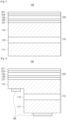
- FIG. 1 is a view for describing an LED device according to an embodiment.
- an LED device 100 includes a first semiconductor layer 111, a light emitting layer 113, a second semiconductor layer 115 and a filter 120.
- the LED device 100 may refer to a semiconductor device configured to emit light.
- the LED device 100 may be implemented as an inorganic semiconductor-based micro LED device or a mini LED device.
- the micro LED device may refer to a semiconductor light emitting device having width, length and height of 1 to 100 micrometers ( ⁇ m), respectively; and the mini LED device may refer to a semiconductor light emitting device having width, length and height of 100 to 200 micrometers ( ⁇ m), respectively.
- the first semiconductor layer 111 may include a first type semiconductor
- the second semiconductor layer 115 may include a second type semiconductor different from the first type.
- the first type and the second type may refer to different ones of an n-type semiconductor and a p-type semiconductor.
- the first semiconductor layer 111 of the first type is the n-type (or p-type) semiconductor
- the second semiconductor layer 115 of the second type may be the p-type (or n-type) semiconductor.
- the n-type semiconductor may refer to a semiconductor in which a free electron is used as a carrier for transferring electric charge
- the p-type semiconductor may refer to a semiconductor in which a hole is used as the carrier for transferring the electric charge.
- the light emitting layer 113 may be configured to emit light based on a difference between a voltage applied to the first semiconductor layer 111 and a voltage applied to the second semiconductor layer 115. To this end, the light emitting layer 113 may be formed between the first semiconductor layer 111 and the second semiconductor layer 115.
- the light emitting layer may refer to an active layer formed on an interface formed by a junction of the n-type semiconductor and the p-type semiconductor.
- the light emitting layer 113 may be formed of a single-quantum well structure (SQW) or a multi-quantum well structure (MQW).
- the first semiconductor layer 111, the light emitting layer 113 and the second semiconductor layer 115 may form a semiconductor cell 110.
- the filter 120 may be configured to transmit light in a second wavelength band 330 (see FIG. 3B ) within a first wavelength band 310 (see FIG. 3B ).
- the filter 120 may transmit light in the second wavelength band 330 within the first wavelength band 310 and may not transmit the other light by reflecting or absorbing light in a wavelength band other than the second wavelength band 330 within the first wavelength band 310.
- the first wavelength band 310 may include a prohibited band or a prohibited transmission region through which light is not transmitted and the second wavelength band 330.
- the second wavelength band 330 may refer to a pass band through which light is transmitted within the first wavelength band 310.
- the filter 120 may be formed on the second semiconductor layer 115.
- the filter 120 may be formed on a surface of the semiconductor cell 110 from which light is extracted in consideration of a path through which light emitted from inside the semiconductor cell 110 is extracted to the outside. In the disclosure, it is assumed that light emitted from the light emitting layer 113 in the semiconductor cell 110 is extracted to the outside through the second semiconductor layer 115. Therefore, the filter 120 may be formed on the second semiconductor layer 115.
- the filter 120 may include a plurality of first refractive layers 121 and 121', a plurality of second refractive layers 123 and 123' and a defect layer 125.
- first refractive layers 121 and 121' are respectively referred to as the first refractive layers 121
- second refractive layers 123 and 123' are respectively referred to as second refractive layers 123.
- the first refractive layers 121 may have a refractive index smaller than that of the second refractive layers 123. That is, the second refractive layers may have a refractive index greater than a refractive index of the first refractive layers.
- the refractive index may refer to a rate at which a speed of light is decreased in case that light is moved (progressed) to another medium.
- the plurality of first refractive layers 121 and 121' and the plurality of second refractive layers 123 and 123' may be formed alternately with each other on one side and the other side of the defect layer 125.
- one side of the defect layer 125 may refer to a bottom surface of the defect layer 125 and the other side of the defect layer 125 may refer to a top surface of the defect layer 125.
- the alternation of the first and second refractive layers 121 and 123 may refer to one pair of the first and second refractive layers 121 and 123 or a periodical repetition of one pair of the first and second refractive layers 121 and 123.
- the defect layer 125 is an intermediate layer positioned inside the filter 120 and formed between the plurality of first refractive layers 121 and 121' and the plurality of second refractive layers 123 and 123'. Meanwhile, a thickness of the defect layer 125 is determined based on a center wavelength of the first wavelength band 310, a peak wavelength of the second wavelength band 330 and a refractive index of the defect layer 125.
- the center wavelength of the first wavelength band 310 may refer to a wavelength that is an average (or an intermediate value) of a minimum wavelength and a maximum wavelength of the first wavelength band 310
- the peak wavelength of the second wavelength band 330 may refer to a wavelength of light having the greatest amount of transmission in the second wavelength band 330.
- the thickness of the defect layer 125 may have a thickness different from the thicknesses of the first refractive layer and the second refractive layer, which are peripheral layers of the defect layer 125.
- the prohibited band (prohibited transmission region) through which light is not transmitted may be formed in a light transmission spectrum (a function of transmittance for a light wavelength) due to the plurality of first refractive layers 121 and 121' and the plurality of second refractive layers 123 and 123' formed alternately with each other; and the pass band through which light may be transmitted may be formed within the prohibited band in the light transmission spectrum due to the defect layer 125 having the thickness different from the thicknesses of the first refractive layer and the second refractive layer.
- a value of a full width at half maximum (FWHM) of the pass band may have a value of a narrow width in a range of 2 to 50 nm.
- the LED device 100 of the disclosure may transmit light only in the second wavelength band 330, which is the pass band with the narrow width, within the first wavelength band 310, thereby improving color purity of light.
- the LED device 100 of the disclosure has a structure in which the semiconductor cell 110 and the filter 120 are formed integrally to each other, thereby having simplified manufacturing process and structure and the improved color purity of light.
- a display apparatus to which such an LED device is applied may improve the color purity of light extracted from the LED device to the outside, thereby widening a range of colors implemented by a combination of red, green and blue colors.
- the display apparatus may improve color reproducibility which is a measure of whether a real object color may be reproduced on a screen of the display apparatus.
- the LED device 100 of the disclosure may be placed on a display module to be electrically connected to a driving circuit formed on the display module, and the LED device 100 may emit light based on a signal of the driving circuit.
- a plurality of LED devices 100 may be placed on the display module in a matrix form.
- the display module may be installed and applied to an electronic product or an electronic field that requires a wearable device, a portable device, a handheld device and various displays in a single unit, and may be applied to a display apparatus such as a monitor for a personal computer (PC), a high-definition television (TV), a signage and a billboard through a plurality of assembly arrangements in a matrix type.
- PC personal computer
- TV high-definition television
- signage a billboard
- FIG. 2 is a cross-sectional view of an LED device for describing an LED device according to an embodiment.
- the LED device 100 may further include electrodes 130 in addition to the first semiconductor layer 111, the light emitting layer 113, the second semiconductor layer 115 and the filter 120.
- the first semiconductor layer 111 may include the first-type semiconductor
- the second semiconductor layer 115 may include the second-type semiconductor different from the first-type semiconductor.
- the first semiconductor layer 111 and the second semiconductor layer 115 may be formed of at least one layer.
- the layer may have a structure with a smaller height compared to its width and length, which may be referred to as a vertically-formed structure.
- the light emitting layer 113 may be formed between the first semiconductor layer 111 and the second semiconductor layer 115, and may emit light based on the difference between the voltage applied to the first semiconductor layer 111 and the voltage applied to the second semiconductor layer 115.
- the difference between the voltage applied to the n-type semiconductor layer and the voltage applied to the p-type semiconductor layer is equal to or greater than a threshold voltage
- the electron provided in the n-type semiconductor and the hole provided in the p-type semiconductor may be recombined to each other in the light emitting layer 113, and the light emitting layer 113 may thus emit light (photon packet) of a specific wavelength (or specific color) corresponding to band gap energy.
- the difference between the voltage applied to the n-type semiconductor layer and the voltage applied to the p-type semiconductor layer may be referred to as a bias.
- a forward bias may indicate a bias in which a voltage of an anode is applied to the p-type semiconductor layer and a voltage of a cathode is applied to the n-type semiconductor layer; and a reverse bias may indicate a bias in which the voltage of the cathode is applied to the p-type semiconductor layer and the voltage of the anode is applied to the n-type semiconductor layer.
- the threshold voltage (or operating voltage) may be determined differently based on materials and structures of the first semiconductor layer 111 and the second semiconductor layer 115, a light color of the light emitting layer 113, etc.
- the threshold voltage may have a specific value such as +1.8V or +3.4V of the forward bias based on, for example, the materials and structures of the first semiconductor layer 111 and the second semiconductor layer 115, the light color of the light emitting layer 113, etc.
- the light emitting layer 113 may not emit light in case that the difference between the voltage applied to the first semiconductor layer 111 and the voltage applied to the second semiconductor layer 115 is less than the threshold voltage.
- the light emitting layer 113 may emit light of a specific color based on the difference between the voltage applied to the first semiconductor layer 111 and the voltage applied to the second semiconductor layer 115.
- the first and second semiconductor layers 111 and 115 may be formed of various compound semiconductors having specific band gap energy corresponding to a specific wavelength of the spectrum.
- the first and second semiconductor layers 111 and 115 including a compound semiconductor may be formed by growing a crystal with certain directionality on a single crystal wafer such as aluminum oxide (Al 2 O 3 ), silicon (Si), silicon carbide (SiC), gallium arsenide (GaAs), gallium phosphide (GaP) or the like through epitaxy growth.
- the specific band gap energy may be determined based on the compound and a composition ratio of the first and second semiconductor layers 111 and 115 in the semiconductor cell 110, and the light emitting layer 113 may emit light of a specific wavelength (or specific color) corresponding to the band gap energy.
- the red semiconductor cell 110 may include one or more semiconductor layers based on an AllnGaP-based semiconductor to emit red light having a wavelength of 600 to 750 nm.
- the blue and green semiconductor cells 110 may include one or more semiconductor layers based on the AllnGaN-based semiconductor to emit blue and green light having wavelengths of 450 to 490 nm and 500 to 570 nm, respectively.
- the red semiconductor cell 110 only refers to the semiconductor cell 110 that emits red light, and does not refer to the color of the semiconductor cell 110 itself. The same is true for the blue and green semiconductor cells 110.
- the filter 120 may be formed on the second semiconductor layer 115 to transmit light in the second wavelength band 330 within the first wavelength band 310.
- the filter 120 may be formed on a top surface of the second semiconductor layer 115 in consideration of the path in which light emitted from the light emitting layer 113 is extracted to the outside.
- this is only an example, and in case that another layer (e.g., a color conversion layer) is formed between the filter 120 and the second semiconductor layer 115, the filter 120 may be formed on a top surface of the another layer.
- another layer e.g., a color conversion layer
- the electrodes 130 may apply an external voltage to the first semiconductor layer 111 and the second semiconductor layer 115.
- the electrodes 130 may be formed on each one side of the first semiconductor layer 111 and the second semiconductor layer 115, and the electrodes 130 may include a first electrode and a second electrode.
- the first electrode may be formed on a top surface of the first semiconductor layer 111 to be in electrical contact (ohmic contact) with the first semiconductor layer 111
- the second electrode may be formed on the top surface of the second semiconductor layer 115 to be in electrical contact with the second semiconductor layer 115.
- the semiconductor layer in contact with the first electrode and the second electrode is the n-type (or p-type)
- it may be referred to as an n-electrode (or p-electrode).
- the electrodes 130 may be made of a material having high conductivity.
- the electrodes 130 may be made of a metal such as aluminum (Al), titanium (Ti), chromium (Cr), nickel (Ni), palladium (Pd), silver (Ag), germanium (Ge) or gold (Au), or an alloy thereof, and may be made of a conductive oxide such as indium tin oxide (ITO) or zinc oxide (ZnO).
- FIG. 2 illustrates that the electrodes 130 are formed on a bottom surface of the first semiconductor layer 111 and a bottom surface of the second semiconductor layer 115, respectively.
- the placement of the electrodes 130 may be variously modified.
- a structural shape of the LED device 100 may also be changed based on the placement of the electrodes 130. A detailed description thereof is described below with reference to FIGS. 6A , 6B and 6C .
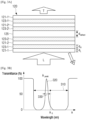
- FIG. 3A is a cross-sectional view of a filter 120 for describing a structure of a filter according to an embodiment.
- FIG. 3B is a view illustrating a light transmission spectrum of a filter for describing a light characteristic of a filter according to an embodiment.
- the filter 120 may be formed on the second semiconductor layer 115 to transmit light in the second wavelength band 330 within the first wavelength band 310.
- the filter 120 to this end may include a plurality of first refractive layers 121-1, 121-2, 121-1' and 121-2', a plurality of second refractive layers 123-1, 123-2, 123-1' and 123-2' and the defect layer 125.
- the plurality of first refractive layers 121-1, 121-2, 121-1' and 121-2' and the plurality of second refractive layers 123-1, 123-2, 123-1' and 123-2' may be formed alternately with each other on one side and the other side of the defect layer 125.
- the first refractive layers 121 and the second refractive layers 123 may be formed alternately (or periodically) and repeatedly on the bottom surface of the defect layer 125, and the first refractive layers 121' and the second refractive layers 123' may be formed alternately and repeatedly on the top surface of the defect layer 125.
- the first refractive layers 121-1 and 121-2 and the second refractive layers 123-1 and 123-2 may be formed alternately with each other between the second semiconductor layer 115 and the defect layer 125 in order of the first refractive layer 121 and the second refractive layer 123.
- the first refractive layers 121-1' and 121-2' and the second refractive layers 123-1' and 123-2' may be formed alternately with each other on the defect layer 125 in order of the second refractive layer 123 and the first refractive layer 121.
- the second refractive layer 123-2', the first refractive layer 121-2', the second refractive layer 123-1', the first refractive layer 121-1', etc. may be repeatedly formed on the defect layer 125.
- the number of the first refractive layers 121-1 and 121-2 and the second refractive layers 123-1 and 123-2 formed on one side of the defect layer 125 may be the same as the number of the first refractive layers 121-1' and 121-2' and the second refractive layers 123-1' and 123-2' formed on the other side of the defect layer 125.
- the first refractive layer 121 and the second refractive layer 123 which are formed on one side of the defect layer 125 has an n number
- the first refractive layer 121' and the second refractive layer 123' which are formed on the other side of the defect layer 125 may have the same n number.
- a total number of the plurality of first refractive layers 121 and 121' and the plurality of second refractive layers 123 and 123' which are included in the filter 120 may be an even number of 2n (here, n is any natural number). Furthermore, assuming that the number of the defect layer 125 is 1, the total number of layers included in the filter 120 may be 2n + 1 (e.g., 5, 7, 9, 11, etc.).
- the plurality of first refractive layers 121-1, 121-2, 121-1' and 121-2' and the plurality of second refractive layers 123-1, 123-2, 123-1' and 123-2' may be formed alternately to be symmetrical to each other with respect to the defect layer 125.
- the order in which the first and second refractive layers 121 and 123 are formed on one side of the defect layer 125 and the order in which the second and first refractive layers 123 and 121 are formed on the other side of the defect layer 125, with respect to the defect layer 125, may be different from each other; and the number of the first and second refractive layers 121 and 123 which are formed on one side of the defect layer 125 and the number of the first and second refractive layers 123 and 121 which are formed on the other side of the defect layer 125 may be the same as each other.
- a thickness d L of the first refractive layer 121 may be determined based on a center wavelength ⁇ 0 of the first wavelength band 310 and a refractive index n L of the first refractive layer 121.
- a thickness d H of the second refractive layer 123 may be determined based on the center wavelength ⁇ 0 of the first wavelength band 310 and a refractive index n H of the second refractive layer 123.
- the thickness d L of the first refractive layer 121 may be determined based on Math Figure 1 below, and the thickness d H of the second refractive layer 123 may be determined based on Math Figure 2 below.
- d L 1 n L ⁇ 0 4
- d H 1 n H ⁇ 0 4
- the first wavelength band 310 may include a wavelength band corresponding to one of red, green and blue colors of light incident on the filter 120.
- the wavelength band may refer to a band between the minimum wavelength and the maximum wavelength.
- the first wavelength band 310 may refer to a band between the minimum wavelength of 420 nm and the maximum wavelength of 500 nm.
- this band is only an embodiment, and the first wavelength band 310 is for forming the prohibited band through which light is not transmitted within the band, and may be variously modified based on a wavelength band of light emitted from the light emitting layer 113.
- the center wavelength ⁇ 0 of the first wavelength band 310 may refer to a wavelength that is the average of the minimum wavelength and the maximum wavelength of the first wavelength band 310.
- the refractive index n L of the first refractive layer 121 may have a value smaller than the refractive index n H of the second refractive layer 123. That is, the refractive index n H of the second refractive layer 123 may have a value greater than the refractive index n L of the first refractive layer 121.
- the first refractive layer 121 may have the refractive index n L of 1.0 or more and 2.0 or less, and the second refractive layer 123 may have the refractive index n H of 2.0 or more and 3.0 or less.
- the first refractive layer 121 may include a material such as silicon dioxide (SiOz), silicon nitride (SiNx), magnesium fluoride (MgF 2 ) or an alloy made of a combination thereof
- the second refractive layer 123 may include of a material such as titanium dioxide (TiOz), niobium pentoxide (Nb 2 O 5 ), tantalum pentoxide (Ta 2 O 5 ) or an alloy made of a combination thereof.
- a thermally and chemically stable resin may be used for the first refractive layer 121 and the second refractive layer 123.
- the defect layer 125 may be formed as an intermediate layer of the filter 120.
- the defect layer 125 may be formed as the intermediate layer in a structure in which the plurality of first refractive layers 121-1, 121-2, 121-1' and 121-2' and the plurality of second refractive layers 123-1, 123-2, 123-1' and123-2' are formed alternately with each other.
- the defect layer 125 may be formed between the plurality of second refractive layers 123-2 and 123-2', and here, a refractive index ndefect of the defect layer 125 may be smaller than the refractive index n H of the second refractive layer 123.
- a thickness ddefect of the defect layer 125 is determined based on a peak wavelength ⁇ p (reference numeral 320) of the second wavelength band 330 and the refractive index ndefect of the defect layer 125.
- the refractive index ndefect of the defect layer 125 is the same as the refractive index n L of the first refractive layer 121. In the description hereinafter, the refractive index ndefect of the defect layer 125 is the same as the refractive index n L of the first refractive layer.
- the thickness ddefect of the defect layer 125 has a value within a range of Math Figure 3 or Math Figure 4 as shown below based on the refractive index n L and the center wavelength ⁇ 0 of the first wavelength band 310. 0 ⁇ d def ect ⁇ 1 n L ⁇ 0 4 1 n L ⁇ 0 4 ⁇ d def ect ⁇ 1 n L 3 ⁇ 0 4
- the thickness ddefect of the defect layer 125 is determined based on (1) or (2) of Math Figure 5 below in case that the thickness ddefect of the defect layer 125 has the above-described range of Math Figure 3 .
- (1) of Math Figure 5 summarizes the peak wavelength ⁇ p of the second wavelength band 330
- (2) of Math Figure 5 summarizes the defect ddefect of the defect layer 125 in (1) of Math Figure 5 .
- the thickness ddefect of the defect layer 125 has a positive value regardless of a sign.
- the thickness ddefect of the defect layer 125 is determined based on the center wavelength ⁇ 0 of the first wavelength band 310, the peak wavelength ⁇ p of the second wavelength band 330 and the refractive index ndefect of the defect layer 125.
- the peak wavelength ⁇ p of the second wavelength band 330 may refer to a wavelength having the greatest amount of light transmitted in the second wavelength band 330 which is the pass band through which light is transmitted.
- the peak wavelength ⁇ p of the second wavelength band 330 and the center wavelength ⁇ 0 of the first wavelength band 310 may have values different from each other.
- the thickness ddefect of the defect layer 125 is determined based on (1) or (2) of Math Figure 6 below in case that the thickness ddefect of the defect layer 125 has the above-described range of Math Figure 4 .
- (1) of Math Figure 6 summarizes the peak wavelength ⁇ p of the second wavelength band 330
- (2) of Math Figure 6 summarizes the defect ddefect of the defect layer 125 in (1) of Math Figure 6 .
- the thickness ddefect of the defect layer 125 has a positive value regardless of a sign.
- the description hereinafter describes an embodiment in which the thicknesses of the first refractive layer 121, the second refractive layer 123 and the defect layer 125 are determined based on the above-described Math Figure.
- the first refractive layer 121 and the defect layer 125 are made of SiO2 having the refractive index n L of about 1.4
- the second refractive layer 123 is made of TiO2 having the refractive index n H of about 2.3.
- the first refractive layer 121 may have the thickness d L of 92.9 nm based on Math Figure 1
- the second refractive layer 123 may have the thickness d H of 56.5 nm based on Math Figure 2 .
- the first refractive layer 121 may have the thickness d L of 107.1 nm based on Math Figure 1
- the second refractive layer 123 may have the thickness d H of 65.2 nm based on Math Figure 2 .
- FIG. 3B illustrates that the center wavelength ⁇ 0 of the first wavelength band 310 is greater than the peak wavelength ⁇ p of the second wavelength band 330.
- this relationship is only an embodiment, and unlike FIG. 3B , the scale relationship between the center wavelength ⁇ 0 of the first wavelength band 310 and the peak wavelength ⁇ p of the second wavelength band 330 may be modified.
- FIGS. 4A, 4B and 4C are views for describing light characteristics of an LED device according to an embodiment.
- light emitted from the light emitting layer 113 of the LED device 100 has a wavelength band (e.g., 420 to 500 nm) corresponding to the blue color.
- FIG. 4A illustrates a light spectrum distribution of a case in which light emitted from the light emitting layer 113 is extracted to the outside in case that the filter 120 is not formed in the LED device 100 according to an embodiment.
- the light spectrum for each of the plurality of LED devices 100 in which the filter 120 is not formed is illustrated by graphs divided into a solid line, a dotted line and a double-dashed line.
- the light spectrum for each of the plurality of LED devices 100 may have a wavelength within 455 to 465 nm as a peak wavelength (wavelength with maximum light intensity).
- the center peak wavelength w p may be 460 nm, which is an average of the peak wavelength
- a difference ⁇ w p in the peak wavelength may be 10 nm, which is the difference between the maximum value 465 nm and minimum value 455 nm of the peak wavelength.
- a value of the FWHM may be 19 nm.
- the value of the FWHM may refer to a difference (interval) between two wavelengths with light intensity of 50% under an assumption that light intensity is 100% at the peak wavelength.
- FIG. 4C is a view describing a light transmission spectrum of the filter 120 according to an embodiment.
- the light transmission spectrum of the filter 120 formed on the LED device 100 may determine the center wavelength of the first wavelength band 310 by adjusting each thickness and refractive index of the first and second refractive layers 121 and 123 based on Math Figures 1 and 2 , and determine the peak wavelength w p of the second wavelength band 330 by adjusting the thickness and refractive index of the defect layer 125 based on Math Figure 5 or Math Figure 6 .
- the peak wavelength w p of the second wavelength band 330 may be determined to be 460 nm, and a value of the FWHM in this case may be 5 nm.
- FIG. 4B illustrates a light spectrum distribution of a case in which light emitted from the light emitting layer 113 is extracted to the outside if the filter 120 is formed in the LED device 100 according to an embodiment.
- the light spectrum may refer to a graph illustrating the relationship of light intensity to a wavelength of light for each of the LED devices 100.
- the light spectrum for each of the plurality of LED devices 100 in which the filter 120 is not formed is illustrated by graphs divided into a solid line, a dotted line and a double-dashed line.
- the light spectrum for each of the plurality of LED devices 100 may have a wavelength within 459 to 461 nm as the peak wavelength.
- the center peak wavelength w p may be 460 nm, which is the average of the peak wavelength
- the difference ⁇ w p in the peak wavelength may be 2 nm, which is the difference between the maximum value 461 nm and minimum value 459 nm of the peak wavelength.
- a value of the FWHM may be 5 nm.
- the light spectrum illustrated in FIG. 4A indicates the light spectrum in case that light emitted from the plurality of LED devices 100 in which the filter 120 is not formed is extracted to the outside.
- the light spectrum illustrated in FIG. 4B illustrated the light spectrum in case that light emitted from the plurality of LED devices 100 in which the filter 120 is formed is incident on the filter 120.
- the light spectrum distribution of a case in which light emitted from the plurality of LED devices 100 in which the filter 120 is formed is extracted to the outside through the filter 120 may be obtained as a result of multiplying the light spectrum illustrated in FIG. 4A by the light transmission spectrum of the filter 120 illustrated in FIG. 4C .
- the prohibited transmission region through which light is not transmitted may be formed in a light transmission spectrum due to the plurality of first refractive layers 121 and 121' and the plurality of second refractive layers 123 and 123' formed alternately with each other; and the pass band through which light may be transmitted may be formed in the prohibited band within the light transmission spectrum due to the defect layer 125 having the thickness different from the thicknesses of the first refractive layer and the second refractive layer.
- the value of the FWHM of the pass band may have a value of the narrow width in the range of 2 to 50 nm.
- the LED device 100 of the disclosure may transmit light only in the second wavelength band 330, which is the pass band with the narrow width, within the first wavelength band 310, thereby improving the color purity of the light.
- FIG. 5A is a view for describing a structure of an LED device according to an embodiment.
- the LED device 100 may further include a reflective layer 140 in addition to the first semiconductor layer 111, the light emitting layer 113, the second semiconductor layer 115 and the filter 120.
- the reflective layer 140 may be configured to reflect light emitted from the light emitting layer 113 to the filter 120.
- the reflective layer 140 may be formed on outer surfaces of the first semiconductor layer 111, the second semiconductor layer 115 and the light emitting layer 113.
- the reflective layer 140 may be formed on the outer surfaces of the first semiconductor layer 111, the second semiconductor layer 115 and the light emitting layer 113, and may further be formed on a sidewall except for a top surface of the filter 120.
- FIG. 5A illustrates that an angle of the reflective layer 140 is 90 degrees based on a horizontal plane.
- this angle is only an embodiment, and the angle may be variously changed (e.g., to an angle within 5 to 85 degrees) with respect to the horizontal plane.
- angles with respect to the side surfaces of the first semiconductor layer 111, the second semiconductor layer 115 and the light emitting layer 113 may also be changed.
- the reflective layer 140 may include a passivation layer 141 and a mirror layer 143.
- the passivation layer 141 may be formed on the surfaces of the first semiconductor layer 111, second semiconductor layer 115 and light emitting layer 113, and may be made of an insulating material (e.g., Al 2 O 3 , SiN, SiO 2 or the like) to protect and electrically insulate the first semiconductor layer 111, the second semiconductor layer 115 and the light emitting layer 113.
- the passivation layer 141 may be made of a transparent insulating material.
- the passivation layer 141 may have an opening region for a portion where the filter 120 is formed, and the filter 120 may thus be formed on the top surface of the second semiconductor layer 115.
- the passivation layer 141 may also have opening regions for portions where the electrodes 130 are formed, respectively, and the electrodes 130 may thus be formed on the top or bottom surfaces of the first semiconductor layer 111 and the second semiconductor layer 115.
- the mirror layer 143 may be formed on a surface of the passivation layer 141.
- the mirror layer 143 may be made by using various materials having high reflectivity.
- the mirror layer 143 may divide the first electrode and the second electrode, which configure the electrodes 130, not to be electrically connected to each other.
- the mirror layer 143 may be formed to have a structure of a metal reflector or that of a distributed-Bragg-reflector (DBR).
- the structure of the distributed-Bragg-reflector may be implemented as a structure of a plurality of layers in which two layers having different refractive indices are stacked alternately with each other.
- Fresnel reflection may thus occur at an interface of each layer due to a difference in refractive indices of the two different layers, and all reflected waves may cause constructive interference based on a material included in the structure of the plurality of layers and its thickness. Accordingly, the mirror layer 143 formed to have the structure of the dispersed-Bragg-reflector may have high reflectivity.
- FIG. 5B is a view for describing a structure of an LED device according to an embodiment.
- the LED device 100 may further include a color conversion layer 150 in addition to the first semiconductor layer 111, the light emitting layer 113, the second semiconductor layer 115 and the filter 120.
- the color conversion layer 150 may be configured to convert a color of light emitted from the light emitting layer 113.
- the color conversion layer 150 may be formed between the second semiconductor layer 115 and the filter 120.
- the color conversion layer 150 may be formed on the top surface of (or inside) the second semiconductor layer 115 and on a bottom surface of the filter 120.
- the color conversion layer 150 may include at least one of a phosphor or a quantum dot (QD).
- the phosphor may refer to an organic or inorganic material that absorbs light emitted from the light emitting layer 113 and emits light of a specific wavelength based on a difference in energy level.
- the quantum dot may refer to an ultrafine semiconductor particle with a diameter of only 2 to 10 nm that emits light of a specific wavelength if exposed to light emitted from the light emitting layer 113.
- the quantum dot may emit light of various colors based on a size of the particle. For example, a quantum dot having a size of 2 nm may emit blue light, and a quantum dot having a size of 6 nm may emit red light.
- FIGS. 6A , 6B and 6C are views for describing structures of an LED device according to an embodiment.
- the LED device 100 may be formed to have various structures according to the placement of the electrodes 130.
- the structure of the LED device 100 may be divided into a lateral type in which the electrodes 130 are placed laterally with respect to the semiconductor cell 110 as illustrated in FIGS. 6A and 6B , and a vertical type in which the electrodes 130 are placed vertically with respect to the semiconductor cell 110 as illustrated in FIG. 6C .
- the lateral type may be divided into a structure in which the electrodes 130 are placed on bottom surfaces of the semiconductor cell 110 as illustrated in FIG. 6A and a structure in which the electrodes 130 are placed on top surfaces of the semiconductor cell 110 as illustrated in FIG. 6A .
- the structure in which the electrodes 130 are placed on the bottom surfaces of the semiconductor cell 110 may be referred to as a flip chip type.
- the structure in which the electrodes 130 of the lateral-type LED device 100 are placed on the top surfaces of the semiconductor cell 110 may hereinafter be referred to as a lateral-type LED device 100; and the structure in which the electrodes 130 are placed on the bottom surfaces of the semiconductor cell 110 may be referred to as a flip-chip type LED device 100.
- the LED device 100 may be formed to have the flip-chip type structure.
- the electrodes 130 may be placed (or formed) on the bottom surfaces of the semiconductor cell 110.
- the first electrode and the second electrode configuring the electrodes 130 may be formed on the bottom surface of the first semiconductor layer 111 and on the bottom surface of the second semiconductor layer 115, respectively.
- the flip-chip type LED device 100 may be bonded and electrically connected to a driving circuit 30 of a display apparatus 10 as illustrated in FIGS. 7A and 7B .
- a bump may be applied between the electrodes 130 of the flip-chip type LED device 100 and electrodes 40 of the driving circuit 30, and the flip-chip type LED device 100 may be bonded to the driving circuit 30 by allowing the applied bump to undergo a curing or firing process by heat at a high or low temperature.
- the bump may be made of a conductive resin.
- the bump may be one of metals such as aluminum (Al), copper (Cu), stannum (Sn), gold (Au), zinc (Zn), lead (Pb) and the like or a mixture or alloy of at least two metals, and implemented as a material in which a powder having an average particle diameter of 0.1 to 10 micrometers and an adhesive paste or a binder resin are mixed with each other.
- metals such as aluminum (Al), copper (Cu), stannum (Sn), gold (Au), zinc (Zn), lead (Pb) and the like or a mixture or alloy of at least two metals, and implemented as a material in which a powder having an average particle diameter of 0.1 to 10 micrometers and an adhesive paste or a binder resin are mixed with each other.
- the LED device 100 may be formed to have the lateral-type structure.
- the electrodes 130 may be placed (or formed) on the top surfaces of the semiconductor cell 110.
- the first electrode and the second electrode configuring the electrodes 130 may be formed on the top surface of the first semiconductor layer 111 and on the top surface of the second semiconductor layer 115, respectively.
- the lateral-type LED device 100 may be electrically connected to the driving circuit 30 of the display apparatus 10 through a wire as illustrated in FIGS. 7A and 7B .
- the LED device 100 may be formed to have the vertical-type structure.
- the electrodes 130 may be placed (or formed) on the top and bottom surfaces of the semiconductor cell 110, respectively.
- the first electrode and the second electrode configuring the electrodes 130 may be formed on the bottom surface of the first semiconductor layer 111 and on the top surface of the second semiconductor layer 115, respectively.
- the vertical-type LED device 100 may be electrically connected to the driving circuit 30 of the display apparatus 10 through the wire, the bump or a combination thereof as illustrated in FIGS. 7A and 7B .
- FIGS. 7A and 7B are views for describing a display apparatus to which an LED device according to an embodiment is applied.
- FIG. 7A is a plan view of the display apparatus 10 and a pixel 20
- FIG. 7B is a cross-sectional view of the pixel 20.
- the display apparatus 10 may include at least one pixel 20.
- the display apparatus 10 is an apparatus capable of processing an image signal received from an external apparatus or an internal storage apparatus (not illustrated) and visually display the processed image, and may be implemented in various forms such as a television (TV), a monitor, a portable multimedia apparatus, a portable communication apparatus, a smartphone, a smart window, a head mount display (HMD), a wearable apparatus, a signage, etc.
- TV television
- HMD head mount display
- the display apparatus 10 may include at least one pixel 20.
- the display apparatus 10 is an apparatus capable of processing an image signal received from an external apparatus or an internal storage apparatus (not illustrated) and visually display the processed image, and may be implemented in various forms such as a television (TV), a monitor, a portable multimedia apparatus, a portable communication apparatus, a smartphone, a smart window, a head mount display (HMD), a wearable apparatus, a signage, etc.
- TV television
- HMD head mount display
- a wearable apparatus a signage
- the pixel 20 may refer to a unit configuring the image displayed by the display apparatus 10.
- the pixels 20 may be arranged in a horizontal and vertical matrix form.
- the pixel 20 may be configured of a plurality of sub-pixels.
- the pixel 20 may represent light of a specific color and brightness by a combination of sub-pixels of red (R), green (G) and blue (B) colors, which are three components of light.
- the plurality of sub-pixels (R, G and B) configuring the pixel 20 may be arranged in different sizes and positions based on various types such as a first type 21 and a second type 22.
- the sizes, positions, arrangements and the like of the plurality of sub-pixels may be variously changed based on various types of layouts such as diamond type, delta type, stripe type, RGBW (red, green, blue and white) type, RGBY (red, green, blue and yellow) type, pen-tile type, quad type, mosaic type, etc. Accordingly, the number, arrangement, structure and color of the LED device configuring the sub-pixel may also be variously changed.
- the pixel 20 may be implemented by a driving of a plurality of LED devices 100-1, 100-2 and 100-3. That is, the sub-pixel may be implemented by the driving of the LED device 100.
- the sub-pixel may be implemented by the driving of the LED device 100.
- a red sub-pixel R may be implemented by the driving of the red LED device 100-1
- a green sub-pixel G may be implemented by the driving of the green LED device 100-2
- a blue sub-pixel B may implemented by the driving of the blue LED device 100-3.
- the plurality of LED devices 100-1, 100-2 and 100-3 have only the difference in a color of the light emitted from each device, and the description of the LED device 100 according to an embodiment may be equally applied thereto.
- the display apparatus 10 may include the driving circuit 30 for driving the plurality of LED devices 100-1, 100-2 and 100-3.
- the driving circuit 30 may be formed inside or on a substrate (not illustrated) of the display apparatus 10.
- the driving circuit 30 may apply a forward voltage (e.g., a voltage of an anode applied to the p-type semiconductor and a voltage of a cathode applied to the n-type semiconductor) or a reverse voltage (e.g., a voltage of the cathode applied to the p-type semiconductor and a voltage of the anode to the n-type semiconductor) to each of the plurality of LED devices 100-1, 100-2 and 100-3.
- the driving circuit 30 may individually control the driving (light emission) of the plurality of LED devices 100-1, 100-2 and 100-3.
- the plurality of LED devices 100-1, 100-2 and 100-3 may be mounted on the driving circuit 30, and the electrodes 130 of the plurality of LED devices 100-1, 100-2 and 100-3 and the electrodes 40 of the driving circuit 30 may be electrically connected to each other.
- the driving circuit 30 may include individual electrodes (not illustrated) and a common electrode (not illustrated) that are electrically separated (or insulated) from each other, and the individual electrodes and common electrode of the driving circuit 30 may be electrically connected to the first and second electrodes of the plurality of LED devices 100-1, 100-2 and 100-3, respectively.
- the individual electrodes may be implemented as switching devices separately connected to each of the LED devices 100-1, 100-2 and 100-3 to apply independent voltages thereto, respectively.
- the switching device is a thin film transistor (TFT)
- the TFT may control a specific voltage to be applied to (i.e. in an on state) or not to be applied (i.e. in an off state) to the first electrode of the LED device 100 based on a gate voltage.
- the TFT (or backplane) is not limited to a specific structure or type.
- the TFT may be implemented as a low-temperature polycrystalline silicon (LTPS) TFT, an oxide TFT, a poly silicon TFT, an a-silicon (amorphous silicon) TFT, an organic TFT, a graphene TFT or the like, and may be implemented in various types such as a P-type (or N-type) power metal oxide semiconductor field effect transistor (MOSFET) formed in a silicon (Si)-wafer complementary metal oxide semiconductor (CMOS) process.
- LTPS low-temperature polycrystalline silicon
- MOSFET metal oxide semiconductor field effect transistor
- the common electrode of the plurality of LED devices 100-1, 100-2 and 100-3 may be configured of one electrode commonly connected to the second electrodes of LED devices 100-1, 100-2 and 100-3 to apply a common voltage to the second electrodes of the plurality of LED devices 100-1, 100-2 and 100-3.
- the display apparatus 10 may be driven in a passive matrix or active matrix method, and the driving circuit 30 may be designed based on the driving method of the display apparatus 10.
- the driving circuit 30 may change the intensity (or brightness) of light emitted from the light emitting layer 113 based on a duty ratio of a pulse, and express a gradation by adjusting the duty ratio of the pulse under an assumption that the forward voltage (the voltage of the anode applied to the p-type semiconductor and the voltage of the cathode applied to the n-type semiconductor) based on a pulse width modulation (PWM) method is applied to the first and second semiconductor layers 111 and 115 of the LED device 100.
- PWM pulse width modulation
- the duty ratio may indicate a ratio of time in which the pulse has an on state for one period in case that the pulse has the on (high) state or an off (low) state for the one period.
- FIG. 8 is a flowchart for describing a manufacturing method of an LED device according to an embodiment.
- the manufacturing method of an LED device is described with reference to FIG. 8 and FIGS. 9A, 9B , 9C and 9D together.
- the manufacturing method of an LED device 100 includes: sequentially forming, on a substrate 1000, a first semiconductor layer 1111 of a first type, a light emitting layer 1113 emitting light and a second semiconductor layer 1115 of a second type different from the first type (S810); removing the substrate 1000 (S820); and forming a filter 120 on a portion where the substrate 1000 is removed from the first semiconductor layer 1111, the filter 120 transmitting light in a second wavelength band including a peak wavelength within a first wavelength band 310 (S830). Meanwhile, the first semiconductor layer 1111 and the second semiconductor layer 1115 illustrated in FIGS.
- 9A, 9B, 9C and 9D are named as the first and second layers based on an order in which the semiconductor layers are generated; and the first semiconductor layer 111 and the second semiconductor layer 115 illustrated in FIGS. 1, 2 , 3A, 3B , 4A, 4B , 4C, 5A , 5B, 6A , 6B, 6C , 7A and 7B described above are named as the first and second layers based on a position of the semiconductor layer in a direction from its bottom to top.
- the description of the second semiconductor layer 115 described above may be equally applied to the first semiconductor layer 1111 described below, and the description of the first semiconductor layer 111 described above may be equally applied to the second semiconductor layer 1115.
- the first semiconductor layer 1111 of the first type, the light emitting layer 1113 emitting light and the second semiconductor layer 1115 of the second type different from the first type may be sequentially formed on the substrate 1000 (S810).
- the substrate 1000 may be provided first.
- the substrate 1000 may be a wafer for growing the semiconductor layer.
- the substrate 1000 may be made of a wafer such as sapphire (Al 2 SO 4 ), silicon (Si), silicon carbide (SiC), gallium nitride (GaN), gallium arsenide (GaAs), gallium phosphide (GaP), zinc oxide (ZnO), etc.
- the substrate 1000 used in the disclosure is not limited to a specific material.
- the first semiconductor layer 1111, the light emitting layer 1113 emitting light and the second semiconductor layer 1115 may be sequentially formed on the substrate 1000 (S810).
- the first semiconductor layer 1111 may be the first type semiconductor layer
- the second semiconductor layer 1115 may be the second type semiconductor layer different from the first type.
- the first semiconductor layer 1111, the light emitting layer 1113 emitting light and the second semiconductor layer 1115 may be sequentially formed on the substrate 1000 through epitaxial growth utilizing a process technology such as metal organic vapor phase epitaxy (MOVPE), metal organic chemical vapor deposition (MOCVD) or molecular beam epitaxy (MBE).
- MOVPE metal organic vapor phase epitaxy
- MOCVD metal organic chemical vapor deposition
- MBE molecular beam epitaxy
- the first semiconductor layer 1111 of the first type is an n-type semiconductor layer
- the second semiconductor layer 1115 of the second type may be a p-type semiconductor layer
- the first semiconductor layer 1111 of the first type is the p-type semiconductor layer
- the second semiconductor layer 1115 of the second type may be the n-type semiconductor layer.
- semiconductor layers of various characteristics may be additionally stacked on top surfaces or bottom surfaces of the first semiconductor layer 1111 and the second semiconductor layer 1115.
- electrodes 130 may be formed to be in electrical contact (ohmic contact) with the first semiconductor layer 1111 and the second semiconductor layer 1115 to apply an external voltage to the first semiconductor layer 1111 and the second semiconductor layer 1115.
- the electrodes 130 may be formed on each one side of the first semiconductor layer 1111 and the second semiconductor layer 1115, respectively.
- a first electrode of the electrodes 130 may be formed on one side of the first semiconductor layer 1111 and a second electrode separated from the first electrode may be formed on one side of the second semiconductor layer 1115 to electrically separate (insulate) the first semiconductor layer 1111 and the second semiconductor layer 1115 from each other.
- the electrodes 130 may be formed by various techniques such as sputtering, evaporation, and spin coating.
- the semiconductor layer 1100 formed on the substrate 1000 may be etched based on structure and size of the LED device 100.
- the semiconductor layer 1100 may be divided into a plurality of isolated semiconductor cells 1100-1 and 1100-2 to 1100-n by etching at a predetermined interval.
- a size of the isolated semiconductor cells may be in a range of several nanometers to several tens of micrometers.
- the inside of each of the plurality of semiconductor cells 1100-1 and 1100-2 to 1100-n may be formed to have an inverted structure of a semiconductor cell 110 of the LED device 100 according to various embodiments of the disclosure illustrated in FIGS. 5A , 5B , 6A , 6B, 6C , etc.
- the isolation of such semiconductor cells may be achieved by various techniques such as dry etching and plasma etching.
- the manufacturing method of the disclosure may further include forming a reflective layer 140 reflecting light emitted from the light emitting layer 1113 to a filter 120 to be formed as below on outer surfaces of the first semiconductor layer (not illustrated), the second semiconductor layer (not illustrated) and the light emitting layer (not illustrated).
- the reflective layer 140 may be formed on the outer surfaces of the first semiconductor layer 1111, the second semiconductor layer 1115 and the light emitting layer 1113, included in each of the plurality of isolated semiconductor cells 1100-1 and 1100-2 to 1100-n.
- the reflective layer 140 may be formed on the outer surfaces of the first semiconductor layer 1111, the second semiconductor layer 1115 and the light emitting layer 1113 to have various angles such as 1 to 90 degrees with respect to a horizontal plane.
- the reflective layer 140 may be formed by techniques such as atomic layer deposition (ALD), e-beam evaporation, sputtering, and spin coating.
- the substrate 1000 may be removed (S820).
- the substrate 1000 may be removed from the plurality of semiconductor cells 1100-1 and 1100-2 to 1100-n after the semiconductor layer 1100 is isolated into the plurality of semiconductor cells 1100-1 and 1100-2 to 1100-n (S820). Accordingly, the substrate 1000 may be removed by a technique known to those skilled in the art, such as laser lift off or dry or wet etching.
- the plurality of semiconductor cells 1110-1 and 1110-2 to 1110-n may be transferred to a carrier substrate 1200.
- the plurality of semiconductor cells 1110-1 and 1110-2 to 1110-n may be transferred in such a manner that the electrodes 130 are placed on the bottom surfaces of the semiconductor cells.
- the semiconductor layers respectively formed on the plurality of semiconductor cells 1100-1 and 1100-2 to 1100-n may be placed from bottom to top in order of the second semiconductor layer 1115, the light emitting layer 1113 and the first semiconductor layer 1111.
- the manufacturing method of the disclosure may further include, before the forming of the filter 120, forming a color conversion layer 150 including at least one of a phosphor or a quantum dot on the first semiconductor layer 1111.
- the color conversion layer 150 may be configured to convert a color of light emitted from the light emitting layer 113.
- the color conversion layer 150 may be formed between the first semiconductor layer 1111 and the filter 120 to be formed as below. A detailed content is omitted because it overlaps with the above description.
- the filter 120 may be formed on a portion where the substrate 1000 is removed from the first semiconductor layer 1111 (S830), e.g., on the plurality of semiconductor cells 1120-1 and 1120-2 to 1120-n.
- the filter 120 may transmit light in a second wavelength band 330 including the peak wavelength within the first wavelength band 310, and may include a plurality of first refractive layers 121 and a plurality of second refractive layers 123 having a refractive index greater than a refractive index of the first refractive layers.
- the plurality of first refractive layers 121 and the plurality of second refractive layers 123 may be formed alternately with each other on the portion where the substrate 1000 is removed from the first semiconductor layer 1111.
- a defect layer 125 may be formed to be positioned between the plurality of first refractive layers 121 and the plurality of second refractive layers 123.
- the plurality of first refractive layers 121 and the plurality of second refractive layers 123 may be formed alternately with each other on one side and the other side of the defect layer 125.
- the forming of the filter 120 may include: forming the plurality of first refractive layers 121 and the plurality of second refractive layers 123 alternately with each other on the first semiconductor layer 1111 in order of the first refractive layer 121 and the second refractive layer 123; forming the defect layer 125 on a topmost surface of the plurality of first refractive layers 121 and the plurality of second refractive layers 123 formed alternately with each other; and forming the plurality of first refractive layers 121 and the plurality of second refractive layers 123 alternately with each other on the defect layer 125 in order of the second refractive layer 123 and the first refractive layer 121.
- the plurality of first refractive layers 121, the plurality of second refractive layers 123 and the defect layer 125 may be formed on the portion where the substrate 1000 is removed from the first semiconductor layer 1111 in the same order of the first refractive layer 121, the second refractive layer 123, the defect layer 125, the second refractive layer 123 and the first refractive layer 121.
- a thickness of the first refractive layer 121 may be determined based on a center wavelength of the first wavelength band 310 and the refractive index of the first refractive layer 121, and a thickness of the second refractive layer 123 may be determined based on the center wavelength of the first wavelength band 310 and the refractive index of the second refractive layer 123.
- the first refractive layer 121 may have the refractive index of 1.0 or more and 2.0 or less
- the second refractive layer 123 may have the refractive index of 2.0 or more and 3.0 or less.
- a thickness of the defect layer 125 is determined based on the center wavelength of the first wavelength band 310, the peak wavelength of the second wavelength band 330 and a refractive index of the defect layer 125.
- the refractive index of the defect layer 125 is the same as the refractive index of the first refractive layer 121.
- the number of the first refractive layer 121 and the second refractive layer 123 formed on one side of the defect layer 125 may be the same as the number of the first refractive layer 121 and the second refractive layer 123 formed on the other side of the defect layer 125.
- the first wavelength band 310 may include a wavelength band corresponding to one of red, green and blue colors of light incident on the filter.
- the LED device capable of improving the color characteristic of light and the manufacturing method thereof.
- the LED device capable of improving color purity and color reproducibility of light and the manufacturing method thereof.
- the various embodiments of the disclosure may be implemented in software including an instruction stored in a machine-readable storage medium (for example, a computer-readable storage medium).
- a machine may be an apparatus that invokes the stored instruction from the storage medium and may be operated depending on the invoked instruction, and may include the electronic apparatus (for example, the LED device 100) according to the disclosed embodiments.
- the instruction is performed by a processor, the processor may perform a function corresponding to the instruction directly or using other components under a control of the processor.
- the instruction may include codes provided or performed by a compiler or an interpreter.
- the machine-readable storage medium may be provided in a form of a non-transitory storage medium.
- the term 'non-transitory' may indicate that the storage medium is tangible without including a signal, and does not distinguish whether data are semi-permanently or temporarily stored in the storage medium.
- a method may be provided as being included in a computer program product.
- the computer program product may be traded as a product between a seller and a purchaser.
- the computer program product may be distributed in a form of the machine-readable storage medium (for example, a compact disc read only memory (CD-ROM)) that may be read by the machine or online through an application store (for example, PLAYSTORETM).
- an application store for example, PLAYSTORETM
- at least portions of the computer program products may be at least temporarily stored or provided in a storage medium such as a memory of a server of a manufacturer, a server of an application store or a relay server.
- Each of components may include a single entity or a plurality of entities, and some of the sub-components described above may be omitted or other sub-components may be further included in the various embodiments.
- some of the components may be integrated into one entity, and may perform functions performed by the respective components before being integrated in the same or similar manner.
- Operations performed by the modules, the programs or other components, according to various embodiments may be executed sequentially, in parallel, iteratively or heuristically. Alternatively, at least some of the operations may be executed in a different order or omitted, or another operation may be added thereto.
Landscapes
- Physics & Mathematics (AREA)
- General Physics & Mathematics (AREA)
- Optics & Photonics (AREA)
- Led Devices (AREA)
Description
- The present invention relates to a light emitting diode (LED) device and a manufacturing method thereof, and more particularly, to an LED device capable of improving a color characteristic of light and a manufacturing method thereof.
- In recent years, a semiconductor-based light emitting diode (LED) device has been put into practical use in various industries such as display and lighting industries because of high light-emitting efficiency. In particular, a micro LED (µ-LED) device, which has a long lifetime and may form an individual pixel, has been spotlighted as a next-generation light source. Here, the micro LED device may refer to the LED device having width, length and height of 1 to 100 micrometers (µm), respectively.
- Meanwhile, an image displayed on a display apparatus may be formed by a plurality of pixels. Here, the pixel may be formed of sub-pixels representing red (R), green (G) and blue (B) colors, which are three primary colors of light. The pixel may express a variety of colors through an amount of light and a combination of colors of light represented by respective sub-pixels.
- To this end, the micro LED device may be driven individually as a sub-pixel unit (or pixel unit) to emit light to implement the sub-pixel (or pixel). For example, in case that one micro LED device implements one sub-pixel, about 25 million micro LEDs may be required in an ultra high definition (UHD) standard (e.g., the number of pixels of 3840 x 2160).
- Patent documents
US 2012/025244 A1 ,US 2016/087159 A1 ,KR 10-2004-0082786 A JP 2004-279933 A1 KR 2014-0050396 A - There is provided an LED device in accordance with claim 1 and a method of manufacturing an LED in accordance with claim 8. Other aspects of the invention are set forth in the dependent claims.
- The above and other aspects, features and advantages of certain embodiments of the present invention will be more apparent from the following detailed description, taken in conjunction with the accompanying drawings, in which:
-
FIG. 1 is a view for describing an LED device according to an embodiment; -
FIG. 2 is a view for describing an LED device according to an embodiment; -
FIG. 3A is a view for describing a structure of a filter according to an embodiment; -
FIG. 3B is a view for describing a light characteristic of a filter according to an embodiment; -
FIG. 4A is a view for describing a light characteristic of an LED device according to an embodiment; -
FIG. 4B is a view for describing a light characteristic of an LED device according to an embodiment; -
FIG. 4C is a view for describing a light characteristic of an LED device according to an embodiment; -
FIG. 5A is a view for describing a structure of an LED device according to an embodiment; -
FIG. 5B is a view for describing a structure of an LED device according to an embodiment; -
FIG. 6A is a view for describing a structure of an LED device according to an embodiment; -
FIG. 6B is a view for describing a structure of an LED device according to an embodiment; -
FIG. 6C is a view for describing a structure of an LED device according to an embodiment; -
FIG. 7A is a view for describing a display apparatus to which an LED device according to an embodiment is applied; -
FIG. 7B is a view for describing a display apparatus to which an LED device according to an embodiment is applied; -
FIG. 8 is a flowchart for describing a manufacturing method of an LED device according to an embodiment; -
FIG. 9A is a view for describing a manufacturing method of an LED device according to an embodiment; -
FIG. 9B is a view for describing a manufacturing method of an LED device according to an embodiment; -
FIG. 9C is a view for describing a manufacturing method of an LED device according to an embodiment; and -
FIG. 9D is a view for describing a manufacturing method of an LED device according to an embodiment. - Embodiments of the present invention provide an LED device capable of improving a color characteristic of light and a manufacturing method thereof.
- In describing the disclosure, if it is decided that a detailed description for the known functions or configurations related to the disclosure may unnecessarily obscure the gist of the disclosure, its detailed description is omitted. In addition, the following embodiments may be modified in several different forms without departing from the scope of the invention as defined by the claims.
- It is to be understood that technologies mentioned in the disclosure are not limited to specific embodiments, but include all modifications, equivalents, and substitutions according to the embodiments of the disclosure. Throughout the accompanying drawings, similar components are denoted by similar reference numerals.
- As used herein, the terms "1st" or "first", "2nd" or "second" or the like, may use corresponding components regardless of importance or order and are used to distinguish one component from another without limiting the components.
- In the disclosure, an expression "A or B", "at least one of A and/or B", "one or more of A and/or B" or the like, may include all possible combinations of items enumerated together. For example, "A or B", "at least one of A and B" or "at least one of A or B" may indicate all of 1) a case in which at least one A is included, 2) a case in which at least one B is included or 3) a case in which both of at least one A and at least one B are included.
- In the disclosure, expressions such as "x ~ y" and "x-y" may be interpreted to indicate "at least one value belonging to a range of x or more and y or less". (Here, x and y are numbers, respectively).
- In the disclosure, singular forms include plural forms unless the context clearly indicates otherwise. It is further understood that a term 'include' or 'formed of" used in the specification specifies the presence of features, numerals, steps, operations, components, parts or combinations thereof, which is mentioned in the specification, and does not preclude the presence or addition of one or more other features, numerals, steps, operations, components, parts or combinations thereof.
- Meanwhile, various elements and regions in the drawings are schematically illustrated. Therefore, the scope of the invention as defined by the claims is not limited by relative sizes or intervals illustrated in the accompanying drawings.
- Hereinafter, diverse embodiments of the disclosure are described in detail with reference to the accompanying drawings.
-
FIG. 1 is a view for describing an LED device according to an embodiment. - Referring to
FIG. 1 , anLED device 100 according to an embodiment includes afirst semiconductor layer 111, alight emitting layer 113, asecond semiconductor layer 115 and afilter 120. - The
LED device 100 may refer to a semiconductor device configured to emit light. For example, theLED device 100 may be implemented as an inorganic semiconductor-based micro LED device or a mini LED device. Here, the micro LED device may refer to a semiconductor light emitting device having width, length and height of 1 to 100 micrometers (µm), respectively; and the mini LED device may refer to a semiconductor light emitting device having width, length and height of 100 to 200 micrometers (µm), respectively. - The
first semiconductor layer 111 may include a first type semiconductor, and thesecond semiconductor layer 115 may include a second type semiconductor different from the first type. Here, the first type and the second type may refer to different ones of an n-type semiconductor and a p-type semiconductor. For example, in case that thefirst semiconductor layer 111 of the first type is the n-type (or p-type) semiconductor, thesecond semiconductor layer 115 of the second type may be the p-type (or n-type) semiconductor. In this case, the n-type semiconductor may refer to a semiconductor in which a free electron is used as a carrier for transferring electric charge, and the p-type semiconductor may refer to a semiconductor in which a hole is used as the carrier for transferring the electric charge. - The
light emitting layer 113 may be configured to emit light based on a difference between a voltage applied to thefirst semiconductor layer 111 and a voltage applied to thesecond semiconductor layer 115. To this end, thelight emitting layer 113 may be formed between thefirst semiconductor layer 111 and thesecond semiconductor layer 115. Here, the light emitting layer may refer to an active layer formed on an interface formed by a junction of the n-type semiconductor and the p-type semiconductor. In addition, thelight emitting layer 113 may be formed of a single-quantum well structure (SQW) or a multi-quantum well structure (MQW). - Meanwhile, the
first semiconductor layer 111, thelight emitting layer 113 and thesecond semiconductor layer 115 may form asemiconductor cell 110. - The
filter 120 may be configured to transmit light in a second wavelength band 330 (seeFIG. 3B ) within a first wavelength band 310 (seeFIG. 3B ). For example, thefilter 120 may transmit light in thesecond wavelength band 330 within thefirst wavelength band 310 and may not transmit the other light by reflecting or absorbing light in a wavelength band other than thesecond wavelength band 330 within thefirst wavelength band 310. - Here, the
first wavelength band 310 may include a prohibited band or a prohibited transmission region through which light is not transmitted and thesecond wavelength band 330. Here, thesecond wavelength band 330 may refer to a pass band through which light is transmitted within thefirst wavelength band 310. - To this end, the
filter 120 may be formed on thesecond semiconductor layer 115. In detail, thefilter 120 may be formed on a surface of thesemiconductor cell 110 from which light is extracted in consideration of a path through which light emitted from inside thesemiconductor cell 110 is extracted to the outside. In the disclosure, it is assumed that light emitted from thelight emitting layer 113 in thesemiconductor cell 110 is extracted to the outside through thesecond semiconductor layer 115. Therefore, thefilter 120 may be formed on thesecond semiconductor layer 115. - In addition, the
filter 120 may include a plurality of firstrefractive layers 121 and 121', a plurality of secondrefractive layers 123 and 123' and adefect layer 125. Hereinafter, for convenience of explanation, the plurality of firstrefractive layers 121 and 121' are respectively referred to as the firstrefractive layers 121, and the plurality of secondrefractive layers 123 and 123' are respectively referred to as secondrefractive layers 123. - The first
refractive layers 121 may have a refractive index smaller than that of the secondrefractive layers 123. That is, the second refractive layers may have a refractive index greater than a refractive index of the first refractive layers. Here, the refractive index may refer to a rate at which a speed of light is decreased in case that light is moved (progressed) to another medium. - The plurality of first
refractive layers 121 and 121' and the plurality of secondrefractive layers 123 and 123' may be formed alternately with each other on one side and the other side of thedefect layer 125. Here, one side of thedefect layer 125 may refer to a bottom surface of thedefect layer 125 and the other side of thedefect layer 125 may refer to a top surface of thedefect layer 125. In addition, the alternation of the first and secondrefractive layers refractive layers refractive layers - The
defect layer 125 is an intermediate layer positioned inside thefilter 120 and formed between the plurality of firstrefractive layers 121 and 121' and the plurality of secondrefractive layers 123 and 123'. Meanwhile, a thickness of thedefect layer 125 is determined based on a center wavelength of thefirst wavelength band 310, a peak wavelength of thesecond wavelength band 330 and a refractive index of thedefect layer 125. Here, the center wavelength of thefirst wavelength band 310 may refer to a wavelength that is an average (or an intermediate value) of a minimum wavelength and a maximum wavelength of thefirst wavelength band 310, and the peak wavelength of thesecond wavelength band 330 may refer to a wavelength of light having the greatest amount of transmission in thesecond wavelength band 330. In this case, the thickness of thedefect layer 125 may have a thickness different from the thicknesses of the first refractive layer and the second refractive layer, which are peripheral layers of thedefect layer 125. - As such, the prohibited band (prohibited transmission region) through which light is not transmitted may be formed in a light transmission spectrum (a function of transmittance for a light wavelength) due to the plurality of first
refractive layers 121 and 121' and the plurality of secondrefractive layers 123 and 123' formed alternately with each other; and the pass band through which light may be transmitted may be formed within the prohibited band in the light transmission spectrum due to thedefect layer 125 having the thickness different from the thicknesses of the first refractive layer and the second refractive layer. Here, a value of a full width at half maximum (FWHM) of the pass band may have a value of a narrow width in a range of 2 to 50 nm. - Therefore, the
LED device 100 of the disclosure may transmit light only in thesecond wavelength band 330, which is the pass band with the narrow width, within thefirst wavelength band 310, thereby improving color purity of light. - In addition, the
LED device 100 of the disclosure has a structure in which thesemiconductor cell 110 and thefilter 120 are formed integrally to each other, thereby having simplified manufacturing process and structure and the improved color purity of light. A display apparatus to which such an LED device is applied may improve the color purity of light extracted from the LED device to the outside, thereby widening a range of colors implemented by a combination of red, green and blue colors. In addition, the display apparatus may improve color reproducibility which is a measure of whether a real object color may be reproduced on a screen of the display apparatus. - In addition, the
LED device 100 of the disclosure may be placed on a display module to be electrically connected to a driving circuit formed on the display module, and theLED device 100 may emit light based on a signal of the driving circuit. In this case, a plurality ofLED devices 100 may be placed on the display module in a matrix form. Here, the display module may be installed and applied to an electronic product or an electronic field that requires a wearable device, a portable device, a handheld device and various displays in a single unit, and may be applied to a display apparatus such as a monitor for a personal computer (PC), a high-definition television (TV), a signage and a billboard through a plurality of assembly arrangements in a matrix type. - Hereinafter, an LED device according to an embodiment is described in detail with reference to
FIGS. 2 ,3A ,3B ,4A ,4B ,5A ,5B, 6A ,6B and 6C . -
FIG. 2 is a cross-sectional view of an LED device for describing an LED device according to an embodiment. - Referring to
FIG. 2 , theLED device 100 according to an embodiment may further includeelectrodes 130 in addition to thefirst semiconductor layer 111, thelight emitting layer 113, thesecond semiconductor layer 115 and thefilter 120. - The
first semiconductor layer 111 may include the first-type semiconductor, and thesecond semiconductor layer 115 may include the second-type semiconductor different from the first-type semiconductor. Thefirst semiconductor layer 111 and thesecond semiconductor layer 115 may be formed of at least one layer. Here, the layer may have a structure with a smaller height compared to its width and length, which may be referred to as a vertically-formed structure. - The
light emitting layer 113 may be formed between thefirst semiconductor layer 111 and thesecond semiconductor layer 115, and may emit light based on the difference between the voltage applied to thefirst semiconductor layer 111 and the voltage applied to thesecond semiconductor layer 115. - In detail, in case that the difference between the voltage applied to the n-type semiconductor layer and the voltage applied to the p-type semiconductor layer is equal to or greater than a threshold voltage, the electron provided in the n-type semiconductor and the hole provided in the p-type semiconductor may be recombined to each other in the
light emitting layer 113, and thelight emitting layer 113 may thus emit light (photon packet) of a specific wavelength (or specific color) corresponding to band gap energy. Here, the difference between the voltage applied to the n-type semiconductor layer and the voltage applied to the p-type semiconductor layer may be referred to as a bias. A forward bias may indicate a bias in which a voltage of an anode is applied to the p-type semiconductor layer and a voltage of a cathode is applied to the n-type semiconductor layer; and a reverse bias may indicate a bias in which the voltage of the cathode is applied to the p-type semiconductor layer and the voltage of the anode is applied to the n-type semiconductor layer. In this case, the threshold voltage (or operating voltage) may be determined differently based on materials and structures of thefirst semiconductor layer 111 and thesecond semiconductor layer 115, a light color of thelight emitting layer 113, etc. Here, the threshold voltage may have a specific value such as +1.8V or +3.4V of the forward bias based on, for example, the materials and structures of thefirst semiconductor layer 111 and thesecond semiconductor layer 115, the light color of thelight emitting layer 113, etc. - Meanwhile, the
light emitting layer 113 may not emit light in case that the difference between the voltage applied to thefirst semiconductor layer 111 and the voltage applied to thesecond semiconductor layer 115 is less than the threshold voltage. - In addition, the
light emitting layer 113 may emit light of a specific color based on the difference between the voltage applied to thefirst semiconductor layer 111 and the voltage applied to thesecond semiconductor layer 115. To this end, the first and second semiconductor layers 111 and 115 may be formed of various compound semiconductors having specific band gap energy corresponding to a specific wavelength of the spectrum. For example, the first and second semiconductor layers 111 and 115 including a compound semiconductor may be formed by growing a crystal with certain directionality on a single crystal wafer such as aluminum oxide (Al2O3), silicon (Si), silicon carbide (SiC), gallium arsenide (GaAs), gallium phosphide (GaP) or the like through epitaxy growth. - In this case, the specific band gap energy may be determined based on the compound and a composition ratio of the first and second semiconductor layers 111 and 115 in the
semiconductor cell 110, and thelight emitting layer 113 may emit light of a specific wavelength (or specific color) corresponding to the band gap energy. For example, thered semiconductor cell 110 may include one or more semiconductor layers based on an AllnGaP-based semiconductor to emit red light having a wavelength of 600 to 750 nm. In addition, the blue andgreen semiconductor cells 110 may include one or more semiconductor layers based on the AllnGaN-based semiconductor to emit blue and green light having wavelengths of 450 to 490 nm and 500 to 570 nm, respectively. Here, thered semiconductor cell 110 only refers to thesemiconductor cell 110 that emits red light, and does not refer to the color of thesemiconductor cell 110 itself. The same is true for the blue andgreen semiconductor cells 110. - The
filter 120 may be formed on thesecond semiconductor layer 115 to transmit light in thesecond wavelength band 330 within thefirst wavelength band 310. To this end, thefilter 120 may be formed on a top surface of thesecond semiconductor layer 115 in consideration of the path in which light emitted from thelight emitting layer 113 is extracted to the outside. However, this is only an example, and in case that another layer (e.g., a color conversion layer) is formed between thefilter 120 and thesecond semiconductor layer 115, thefilter 120 may be formed on a top surface of the another layer. A more detailed description of thefilter 120 is described below with reference toFIGS. 3A and 3B . - The
electrodes 130 may apply an external voltage to thefirst semiconductor layer 111 and thesecond semiconductor layer 115. To this end, theelectrodes 130 may be formed on each one side of thefirst semiconductor layer 111 and thesecond semiconductor layer 115, and theelectrodes 130 may include a first electrode and a second electrode. For example, the first electrode may be formed on a top surface of thefirst semiconductor layer 111 to be in electrical contact (ohmic contact) with thefirst semiconductor layer 111, and the second electrode may be formed on the top surface of thesecond semiconductor layer 115 to be in electrical contact with thesecond semiconductor layer 115. Here, in case that the semiconductor layer in contact with the first electrode and the second electrode is the n-type (or p-type), it may be referred to as an n-electrode (or p-electrode). - In addition, the
electrodes 130 may be made of a material having high conductivity. For example, theelectrodes 130 may be made of a metal such as aluminum (Al), titanium (Ti), chromium (Cr), nickel (Ni), palladium (Pd), silver (Ag), germanium (Ge) or gold (Au), or an alloy thereof, and may be made of a conductive oxide such as indium tin oxide (ITO) or zinc oxide (ZnO). - Meanwhile,
FIG. 2 illustrates that theelectrodes 130 are formed on a bottom surface of thefirst semiconductor layer 111 and a bottom surface of thesecond semiconductor layer 115, respectively. However, such a placement is only an embodiment, and the placement of theelectrodes 130 may be variously modified. In this case, a structural shape of theLED device 100 may also be changed based on the placement of theelectrodes 130. A detailed description thereof is described below with reference toFIGS. 6A ,6B and 6C . - Hereinafter, a filter according to an embodiment is described in detail with reference to
FIGS. 3A and 3B. FIG. 3A is a cross-sectional view of afilter 120 for describing a structure of a filter according to an embodiment.FIG. 3B is a view illustrating a light transmission spectrum of a filter for describing a light characteristic of a filter according to an embodiment. - The
filter 120 may be formed on thesecond semiconductor layer 115 to transmit light in thesecond wavelength band 330 within thefirst wavelength band 310. - Referring to
FIG. 3A , thefilter 120 to this end may include a plurality of first refractive layers 121-1, 121-2, 121-1' and 121-2', a plurality of second refractive layers 123-1, 123-2, 123-1' and 123-2' and thedefect layer 125. - The plurality of first refractive layers 121-1, 121-2, 121-1' and 121-2' and the plurality of second refractive layers 123-1, 123-2, 123-1' and 123-2' may be formed alternately with each other on one side and the other side of the
defect layer 125. For example, the firstrefractive layers 121 and the secondrefractive layers 123 may be formed alternately (or periodically) and repeatedly on the bottom surface of thedefect layer 125, and the first refractive layers 121' and the second refractive layers 123' may be formed alternately and repeatedly on the top surface of thedefect layer 125. - According to an embodiment, the first refractive layers 121-1 and 121-2 and the second refractive layers 123-1 and 123-2 may be formed alternately with each other between the
second semiconductor layer 115 and thedefect layer 125 in order of the firstrefractive layer 121 and the secondrefractive layer 123. In addition, the first refractive layers 121-1' and 121-2' and the second refractive layers 123-1' and 123-2' may be formed alternately with each other on thedefect layer 125 in order of the secondrefractive layer 123 and the firstrefractive layer 121. For example, the first refractive layer 121-1, the second refractive layer 123-1, the first refractive layer 121-2, the second refractive layer 123-2, etc. may be repeatedly formed between thesecond semiconductor layer 115 and thedefect layer 125. In addition, the second refractive layer 123-2', the first refractive layer 121-2', the second refractive layer 123-1', the first refractive layer 121-1', etc. may be repeatedly formed on thedefect layer 125. - Meanwhile, according to an embodiment, the number of the first refractive layers 121-1 and 121-2 and the second refractive layers 123-1 and 123-2 formed on one side of the
defect layer 125 may be the same as the number of the first refractive layers 121-1' and 121-2' and the second refractive layers 123-1' and 123-2' formed on the other side of thedefect layer 125. For example, if the firstrefractive layer 121 and the secondrefractive layer 123 which are formed on one side of thedefect layer 125 has an n number, the first refractive layer 121' and the second refractive layer 123' which are formed on the other side of thedefect layer 125 may have the same n number. Accordingly, a total number of the plurality of firstrefractive layers 121 and 121' and the plurality of secondrefractive layers 123 and 123' which are included in thefilter 120 may be an even number of 2n (here, n is any natural number). Furthermore, assuming that the number of thedefect layer 125 is 1, the total number of layers included in thefilter 120 may be 2n + 1 (e.g., 5, 7, 9, 11, etc.). - Meanwhile, according to an embodiment, the plurality of first refractive layers 121-1, 121-2, 121-1' and 121-2' and the plurality of second refractive layers 123-1, 123-2, 123-1' and 123-2' may be formed alternately to be symmetrical to each other with respect to the
defect layer 125. That is, the order in which the first and secondrefractive layers defect layer 125 and the order in which the second and firstrefractive layers defect layer 125, with respect to thedefect layer 125, may be different from each other; and the number of the first and secondrefractive layers defect layer 125 and the number of the first and secondrefractive layers defect layer 125 may be the same as each other. - Meanwhile, referring to
FIGS. 3A and 3B , a thickness dL of the firstrefractive layer 121 may be determined based on a center wavelength λ0 of thefirst wavelength band 310 and a refractive index nL of the firstrefractive layer 121. In addition, a thickness dH of the secondrefractive layer 123 may be determined based on the center wavelength λ0 of thefirst wavelength band 310 and a refractive index nH of the secondrefractive layer 123. - For example, the thickness dL of the first
refractive layer 121 may be determined based on MathFigure 1 below, and the thickness dH of the secondrefractive layer 123 may be determined based on MathFigure 2 below.

- Here, the
first wavelength band 310 may include a wavelength band corresponding to one of red, green and blue colors of light incident on thefilter 120. Here, the wavelength band may refer to a band between the minimum wavelength and the maximum wavelength. For example, in the case of the blue color, thefirst wavelength band 310 may refer to a band between the minimum wavelength of 420 nm and the maximum wavelength of 500 nm. However, this band is only an embodiment, and thefirst wavelength band 310 is for forming the prohibited band through which light is not transmitted within the band, and may be variously modified based on a wavelength band of light emitted from thelight emitting layer 113. - In this case, the center wavelength λ0 of the
first wavelength band 310 may refer to a wavelength that is the average of the minimum wavelength and the maximum wavelength of thefirst wavelength band 310. - Meanwhile, the refractive index nL of the first
refractive layer 121 may have a value smaller than the refractive index nH of the secondrefractive layer 123. That is, the refractive index nH of the secondrefractive layer 123 may have a value greater than the refractive index nL of the firstrefractive layer 121. - In an embodiment, the first
refractive layer 121 may have the refractive index nL of 1.0 or more and 2.0 or less, and the secondrefractive layer 123 may have the refractive index nH of 2.0 or more and 3.0 or less. To this end, the firstrefractive layer 121 may include a material such as silicon dioxide (SiOz), silicon nitride (SiNx), magnesium fluoride (MgF2) or an alloy made of a combination thereof, and the secondrefractive layer 123 may include of a material such as titanium dioxide (TiOz), niobium pentoxide (Nb2O5), tantalum pentoxide (Ta2O5) or an alloy made of a combination thereof. Furthermore, a thermally and chemically stable resin may be used for the firstrefractive layer 121 and the secondrefractive layer 123. - Referring to
FIGS. 3A and 3B , thedefect layer 125 may be formed as an intermediate layer of thefilter 120. In detail, thedefect layer 125 may be formed as the intermediate layer in a structure in which the plurality of first refractive layers 121-1, 121-2, 121-1' and 121-2' and the plurality of second refractive layers 123-1, 123-2, 123-1' and123-2' are formed alternately with each other. For example, thedefect layer 125 may be formed between the plurality of second refractive layers 123-2 and 123-2', and here, a refractive index ndefect of thedefect layer 125 may be smaller than the refractive index nH of the secondrefractive layer 123. - A thickness ddefect of the
defect layer 125 is determined based on a peak wavelength λp (reference numeral 320) of thesecond wavelength band 330 and the refractive index ndefect of thedefect layer 125. - In accordance with the present invention, the refractive index ndefect of the
defect layer 125 is the same as the refractive index nL of the firstrefractive layer 121. In the description hereinafter, the refractive index ndefect of thedefect layer 125 is the same as the refractive index nL of the first refractive layer. - According to the present invention, the thickness ddefect of the
defect layer 125 has a value within a range of MathFigure 3 or MathFigure 4 as shown below based on the refractive index nL and the center wavelength λ0 of thefirst wavelength band 310.

- In accordance with the present invention, the thickness ddefect of the
defect layer 125 is determined based on (1) or (2) of MathFigure 5 below in case that the thickness ddefect of thedefect layer 125 has the above-described range of MathFigure 3 . Here, (1) of MathFigure 5 summarizes the peak wavelength λp of thesecond wavelength band 330, and (2) of MathFigure 5 summarizes the defect ddefect of thedefect layer 125 in (1) of MathFigure 5 . In this case, the thickness ddefect of thedefect layer 125 has a positive value regardless of a sign.
- Here, the thickness ddefect of the
defect layer 125 is determined based on the center wavelength λ0 of thefirst wavelength band 310, the peak wavelength λp of thesecond wavelength band 330 and the refractive index ndefect of thedefect layer 125. Here, the peak wavelength λp of thesecond wavelength band 330 may refer to a wavelength having the greatest amount of light transmitted in thesecond wavelength band 330 which is the pass band through which light is transmitted. Here, in order to form thesecond wavelength band 330, the peak wavelength λp of thesecond wavelength band 330 and the center wavelength λ0 of thefirst wavelength band 310 may have values different from each other. - In accordance with the present invention, the thickness ddefect of the
defect layer 125 is determined based on (1) or (2) of MathFigure 6 below in case that the thickness ddefect of thedefect layer 125 has the above-described range of MathFigure 4 . Here, (1) of MathFigure 6 summarizes the peak wavelength λp of thesecond wavelength band 330, and (2) of MathFigure 6 summarizes the defect ddefect of thedefect layer 125 in (1) of MathFigure 6 . In this case, the thickness ddefect of thedefect layer 125 has a positive value regardless of a sign.
- The description hereinafter describes an embodiment in which the thicknesses of the first
refractive layer 121, the secondrefractive layer 123 and thedefect layer 125 are determined based on the above-described Math Figure. Here, it is assumed that the firstrefractive layer 121 and thedefect layer 125 are made of SiO2 having the refractive index nL of about 1.4, and the secondrefractive layer 123 is made of TiO2 having the refractive index nH of about 2.3. - As an embodiment, in case that the light emitted from the
light emitting layer 113 is the blue color, if the center wavelength λ0 of thefirst wavelength band 310 is set to 450 nm, the firstrefractive layer 121 may have the following thickness dL calculated based on MathFigure 1 : (1 / 1.4) x (450 nm / 4) = 80.4 nm, and the secondrefractive layer 123 may have the following thickness dH calculated based on MathFigure 2 : (1 / 2.3) x (450 nm / 4) = 48.9 nm. Here, if the peak wavelength λp of thesecond wavelength band 330 is set to 460 nm, thedefect layer 125 may have the following thickness ddefect calculated based on (2) of MathFigure 5 : (460 nm-450 nm) / (1.4) = 7.1 nm. - In an embodiment, in case that the light emitted from the
light emitting layer 113 is the green color, if the center wavelength λ0 of thefirst wavelength band 310 is set to 520 nm and the peak wavelength λp of thesecond wavelength band 330 is set to 540 nm, the firstrefractive layer 121 may have the thickness dL of 92.9 nm based on MathFigure 1 , and the secondrefractive layer 123 may have the thickness dH of 56.5 nm based on MathFigure 2 . Thedefect layer 125 may have the following thickness ddefect calculated based on (2) of MathFigure 5 : (540 nm - 520 nm) / (1.4) = 14.3 nm. - In an embodiment, in case that the light emitted from the
light emitting layer 113 is the red color, if the center wavelength λ0 of thefirst wavelength band 310 is set to 600 nm and the peak wavelength λp of thesecond wavelength band 330 is set to 650 nm, the firstrefractive layer 121 may have the thickness dL of 107.1 nm based on MathFigure 1 , and the secondrefractive layer 123 may have the thickness dH of 65.2 nm based on MathFigure 2 . Thedefect layer 125 may have the following thickness ddefect calculated based on (2) of MathFigure 5 : (650 nm - 600 nm) / (1.4) = 35.7 nm. - Meanwhile,
FIG. 3B illustrates that the center wavelength λ0 of thefirst wavelength band 310 is greater than the peak wavelength λp of thesecond wavelength band 330. However, this relationship is only an embodiment, and unlikeFIG. 3B , the scale relationship between the center wavelength λ0 of thefirst wavelength band 310 and the peak wavelength λp of thesecond wavelength band 330 may be modified. -
FIGS. 4A, 4B and4C are views for describing light characteristics of an LED device according to an embodiment. Hereinafter, it is assumed that light emitted from thelight emitting layer 113 of theLED device 100 has a wavelength band (e.g., 420 to 500 nm) corresponding to the blue color. -
FIG. 4A illustrates a light spectrum distribution of a case in which light emitted from thelight emitting layer 113 is extracted to the outside in case that thefilter 120 is not formed in theLED device 100 according to an embodiment. Here, the light spectrum for each of the plurality ofLED devices 100 in which thefilter 120 is not formed is illustrated by graphs divided into a solid line, a dotted line and a double-dashed line. - Referring to
FIG. 4A , the light spectrum for each of the plurality ofLED devices 100 may have a wavelength within 455 to 465 nm as a peak wavelength (wavelength with maximum light intensity). In this case, the center peak wavelength wp may be 460 nm, which is an average of the peak wavelength, and a difference Δwp in the peak wavelength may be 10 nm, which is the difference between the maximum value 465 nm and minimum value 455 nm of the peak wavelength. In addition, a value of the FWHM may be 19 nm. Here, the value of the FWHM may refer to a difference (interval) between two wavelengths with light intensity of 50% under an assumption that light intensity is 100% at the peak wavelength. -
FIG. 4C is a view describing a light transmission spectrum of thefilter 120 according to an embodiment. - As described above, the light transmission spectrum of the
filter 120 formed on theLED device 100 according to an embodiment may determine the center wavelength of thefirst wavelength band 310 by adjusting each thickness and refractive index of the first and secondrefractive layers Figures 1 and 2 , and determine the peak wavelength wp of thesecond wavelength band 330 by adjusting the thickness and refractive index of thedefect layer 125 based on MathFigure 5 or MathFigure 6 . For example, as illustrated inFIG. 4C , the peak wavelength wp of thesecond wavelength band 330 may be determined to be 460 nm, and a value of the FWHM in this case may be 5 nm. -
FIG. 4B illustrates a light spectrum distribution of a case in which light emitted from thelight emitting layer 113 is extracted to the outside if thefilter 120 is formed in theLED device 100 according to an embodiment. In this case, the light spectrum may refer to a graph illustrating the relationship of light intensity to a wavelength of light for each of theLED devices 100. Here, the light spectrum for each of the plurality ofLED devices 100 in which thefilter 120 is not formed is illustrated by graphs divided into a solid line, a dotted line and a double-dashed line. - Referring to
FIG. 4B , the light spectrum for each of the plurality ofLED devices 100 may have a wavelength within 459 to 461 nm as the peak wavelength. In this case, the center peak wavelength wp may be 460 nm, which is the average of the peak wavelength, and the difference Δwp in the peak wavelength may be 2 nm, which is the difference between the maximum value 461 nm and minimum value 459 nm of the peak wavelength. In addition, a value of the FWHM may be 5 nm. - Meanwhile, the light spectrum illustrated in
FIG. 4A indicates the light spectrum in case that light emitted from the plurality ofLED devices 100 in which thefilter 120 is not formed is extracted to the outside. The light spectrum illustrated inFIG. 4B illustrated the light spectrum in case that light emitted from the plurality ofLED devices 100 in which thefilter 120 is formed is incident on thefilter 120. In this case, as illustrated inFIG. 4B , the light spectrum distribution of a case in which light emitted from the plurality ofLED devices 100 in which thefilter 120 is formed is extracted to the outside through thefilter 120 may be obtained as a result of multiplying the light spectrum illustrated inFIG. 4A by the light transmission spectrum of thefilter 120 illustrated inFIG. 4C . - As such, the prohibited transmission region through which light is not transmitted may be formed in a light transmission spectrum due to the plurality of first
refractive layers 121 and 121' and the plurality of secondrefractive layers 123 and 123' formed alternately with each other; and the pass band through which light may be transmitted may be formed in the prohibited band within the light transmission spectrum due to thedefect layer 125 having the thickness different from the thicknesses of the first refractive layer and the second refractive layer. Here, the value of the FWHM of the pass band may have a value of the narrow width in the range of 2 to 50 nm. - Therefore, the
LED device 100 of the disclosure may transmit light only in thesecond wavelength band 330, which is the pass band with the narrow width, within thefirst wavelength band 310, thereby improving the color purity of the light. -
FIG. 5A is a view for describing a structure of an LED device according to an embodiment. - Referring to
FIG. 5A , theLED device 100 according to an embodiment may further include areflective layer 140 in addition to thefirst semiconductor layer 111, thelight emitting layer 113, thesecond semiconductor layer 115 and thefilter 120. Here, thereflective layer 140 may be configured to reflect light emitted from thelight emitting layer 113 to thefilter 120. - To this end, the
reflective layer 140 may be formed on outer surfaces of thefirst semiconductor layer 111, thesecond semiconductor layer 115 and thelight emitting layer 113. For example, thereflective layer 140 may be formed on the outer surfaces of thefirst semiconductor layer 111, thesecond semiconductor layer 115 and thelight emitting layer 113, and may further be formed on a sidewall except for a top surface of thefilter 120. - Meanwhile,
FIG. 5A illustrates that an angle of thereflective layer 140 is 90 degrees based on a horizontal plane. However, this angle is only an embodiment, and the angle may be variously changed (e.g., to an angle within 5 to 85 degrees) with respect to the horizontal plane. In this case, as the angle of thereflective layer 140 is changed, angles with respect to the side surfaces of thefirst semiconductor layer 111, thesecond semiconductor layer 115 and thelight emitting layer 113 may also be changed. - Meanwhile, the
reflective layer 140 may include apassivation layer 141 and amirror layer 143. - The
passivation layer 141 may be formed on the surfaces of thefirst semiconductor layer 111,second semiconductor layer 115 and light emittinglayer 113, and may be made of an insulating material (e.g., Al2O3, SiN, SiO2 or the like) to protect and electrically insulate thefirst semiconductor layer 111, thesecond semiconductor layer 115 and thelight emitting layer 113. In addition, thepassivation layer 141 may be made of a transparent insulating material. - Meanwhile, the
passivation layer 141 may have an opening region for a portion where thefilter 120 is formed, and thefilter 120 may thus be formed on the top surface of thesecond semiconductor layer 115. In addition, thepassivation layer 141 may also have opening regions for portions where theelectrodes 130 are formed, respectively, and theelectrodes 130 may thus be formed on the top or bottom surfaces of thefirst semiconductor layer 111 and thesecond semiconductor layer 115. - The
mirror layer 143 may be formed on a surface of thepassivation layer 141. In addition, themirror layer 143 may be made by using various materials having high reflectivity. UnlikeFIG. 5A , in case of being made of a material having high conductivity, such as a metal material (e.g., aluminum (Al)), themirror layer 143 may divide the first electrode and the second electrode, which configure theelectrodes 130, not to be electrically connected to each other. - Meanwhile, the
mirror layer 143 may be formed to have a structure of a metal reflector or that of a distributed-Bragg-reflector (DBR). In detail, the structure of the distributed-Bragg-reflector may be implemented as a structure of a plurality of layers in which two layers having different refractive indices are stacked alternately with each other. In addition, Fresnel reflection may thus occur at an interface of each layer due to a difference in refractive indices of the two different layers, and all reflected waves may cause constructive interference based on a material included in the structure of the plurality of layers and its thickness. Accordingly, themirror layer 143 formed to have the structure of the dispersed-Bragg-reflector may have high reflectivity. -
FIG. 5B is a view for describing a structure of an LED device according to an embodiment. - Referring to
FIG. 5B , theLED device 100 according to an embodiment may further include acolor conversion layer 150 in addition to thefirst semiconductor layer 111, thelight emitting layer 113, thesecond semiconductor layer 115 and thefilter 120. Here, thecolor conversion layer 150 may be configured to convert a color of light emitted from thelight emitting layer 113. - To this end, the
color conversion layer 150 may be formed between thesecond semiconductor layer 115 and thefilter 120. For example, thecolor conversion layer 150 may be formed on the top surface of (or inside) thesecond semiconductor layer 115 and on a bottom surface of thefilter 120. Here, thecolor conversion layer 150 may include at least one of a phosphor or a quantum dot (QD). - Here, the phosphor may refer to an organic or inorganic material that absorbs light emitted from the
light emitting layer 113 and emits light of a specific wavelength based on a difference in energy level. In addition, the quantum dot may refer to an ultrafine semiconductor particle with a diameter of only 2 to 10 nm that emits light of a specific wavelength if exposed to light emitted from thelight emitting layer 113. In particular, the quantum dot may emit light of various colors based on a size of the particle. For example, a quantum dot having a size of 2 nm may emit blue light, and a quantum dot having a size of 6 nm may emit red light. -
FIGS. 6A ,6B and 6C are views for describing structures of an LED device according to an embodiment. - Referring to
FIGS. 6A ,6B and 6C , theLED device 100 according to an embodiment may be formed to have various structures according to the placement of theelectrodes 130. - The structure of the
LED device 100 according to an embodiment may be divided into a lateral type in which theelectrodes 130 are placed laterally with respect to thesemiconductor cell 110 as illustrated inFIGS. 6A and6B , and a vertical type in which theelectrodes 130 are placed vertically with respect to thesemiconductor cell 110 as illustrated inFIG. 6C . The lateral type may be divided into a structure in which theelectrodes 130 are placed on bottom surfaces of thesemiconductor cell 110 as illustrated inFIG. 6A and a structure in which theelectrodes 130 are placed on top surfaces of thesemiconductor cell 110 as illustrated inFIG. 6A . Here, the structure in which theelectrodes 130 are placed on the bottom surfaces of thesemiconductor cell 110 may be referred to as a flip chip type. In this consideration, the structure in which theelectrodes 130 of the lateral-type LED device 100 are placed on the top surfaces of thesemiconductor cell 110 may hereinafter be referred to as a lateral-type LED device 100; and the structure in which theelectrodes 130 are placed on the bottom surfaces of thesemiconductor cell 110 may be referred to as a flip-chiptype LED device 100. - As illustrated in
FIG. 6A , theLED device 100 according to an embodiment may be formed to have the flip-chip type structure. In the flip-chiptype LED device 100, theelectrodes 130 may be placed (or formed) on the bottom surfaces of thesemiconductor cell 110. For example, in the flip-chiptype LED device 100, the first electrode and the second electrode configuring theelectrodes 130 may be formed on the bottom surface of thefirst semiconductor layer 111 and on the bottom surface of thesecond semiconductor layer 115, respectively. - Then, the flip-chip
type LED device 100 may be bonded and electrically connected to a drivingcircuit 30 of adisplay apparatus 10 as illustrated inFIGS. 7A and 7B . For example, a bump may be applied between theelectrodes 130 of the flip-chiptype LED device 100 andelectrodes 40 of the drivingcircuit 30, and the flip-chiptype LED device 100 may be bonded to the drivingcircuit 30 by allowing the applied bump to undergo a curing or firing process by heat at a high or low temperature. To this end, the bump may be made of a conductive resin. For example, the bump may be one of metals such as aluminum (Al), copper (Cu), stannum (Sn), gold (Au), zinc (Zn), lead (Pb) and the like or a mixture or alloy of at least two metals, and implemented as a material in which a powder having an average particle diameter of 0.1 to 10 micrometers and an adhesive paste or a binder resin are mixed with each other. - As illustrated in
FIG. 6B , theLED device 100 according to an embodiment may be formed to have the lateral-type structure. In the lateral-type LED device 100, theelectrodes 130 may be placed (or formed) on the top surfaces of thesemiconductor cell 110. For example, in the lateral-type LED device 100, the first electrode and the second electrode configuring theelectrodes 130 may be formed on the top surface of thefirst semiconductor layer 111 and on the top surface of thesecond semiconductor layer 115, respectively. Then, the lateral-type LED device 100 may be electrically connected to the drivingcircuit 30 of thedisplay apparatus 10 through a wire as illustrated inFIGS. 7A and 7B . - As illustrated in
FIG. 6C , theLED device 100 according to an embodiment may be formed to have the vertical-type structure. In the vertical-type LED device 100, theelectrodes 130 may be placed (or formed) on the top and bottom surfaces of thesemiconductor cell 110, respectively. For example, in the vertical-type LED device 100, the first electrode and the second electrode configuring theelectrodes 130 may be formed on the bottom surface of thefirst semiconductor layer 111 and on the top surface of thesecond semiconductor layer 115, respectively. Then, the vertical-type LED device 100 may be electrically connected to the drivingcircuit 30 of thedisplay apparatus 10 through the wire, the bump or a combination thereof as illustrated inFIGS. 7A and 7B . -
FIGS. 7A and 7B are views for describing a display apparatus to which an LED device according to an embodiment is applied.FIG. 7A is a plan view of thedisplay apparatus 10 and apixel 20, andFIG. 7B is a cross-sectional view of thepixel 20. - Referring to
FIG. 7A , thedisplay apparatus 10 may include at least onepixel 20. Here, thedisplay apparatus 10 is an apparatus capable of processing an image signal received from an external apparatus or an internal storage apparatus (not illustrated) and visually display the processed image, and may be implemented in various forms such as a television (TV), a monitor, a portable multimedia apparatus, a portable communication apparatus, a smartphone, a smart window, a head mount display (HMD), a wearable apparatus, a signage, etc. - The
pixel 20 may refer to a unit configuring the image displayed by thedisplay apparatus 10. Thepixels 20 may be arranged in a horizontal and vertical matrix form. - As illustrated in
FIG. 7A , thepixel 20 may be configured of a plurality of sub-pixels. For example, thepixel 20 may represent light of a specific color and brightness by a combination of sub-pixels of red (R), green (G) and blue (B) colors, which are three components of light. Here, the plurality of sub-pixels (R, G and B) configuring thepixel 20 may be arranged in different sizes and positions based on various types such as afirst type 21 and asecond type 22. However, this arrangement is only an embodiment, and the sizes, positions, arrangements and the like of the plurality of sub-pixels (R, G and B) may be variously changed based on various types of layouts such as diamond type, delta type, stripe type, RGBW (red, green, blue and white) type, RGBY (red, green, blue and yellow) type, pen-tile type, quad type, mosaic type, etc. Accordingly, the number, arrangement, structure and color of the LED device configuring the sub-pixel may also be variously changed. - As illustrated in 7A and 7B, the
pixel 20 may be implemented by a driving of a plurality of LED devices 100-1, 100-2 and 100-3. That is, the sub-pixel may be implemented by the driving of theLED device 100. For example, a red sub-pixel R may be implemented by the driving of the red LED device 100-1, a green sub-pixel G may be implemented by the driving of the green LED device 100-2 and a blue sub-pixel B may implemented by the driving of the blue LED device 100-3. Here, the plurality of LED devices 100-1, 100-2 and 100-3 have only the difference in a color of the light emitted from each device, and the description of theLED device 100 according to an embodiment may be equally applied thereto. - To this end, the
display apparatus 10 according to an embodiment may include the drivingcircuit 30 for driving the plurality of LED devices 100-1, 100-2 and 100-3. - The driving
circuit 30 may be formed inside or on a substrate (not illustrated) of thedisplay apparatus 10. The drivingcircuit 30 may apply a forward voltage (e.g., a voltage of an anode applied to the p-type semiconductor and a voltage of a cathode applied to the n-type semiconductor) or a reverse voltage (e.g., a voltage of the cathode applied to the p-type semiconductor and a voltage of the anode to the n-type semiconductor) to each of the plurality of LED devices 100-1, 100-2 and 100-3. Accordingly, the drivingcircuit 30 may individually control the driving (light emission) of the plurality of LED devices 100-1, 100-2 and 100-3. - To this end, the plurality of LED devices 100-1, 100-2 and 100-3 may be mounted on the driving
circuit 30, and theelectrodes 130 of the plurality of LED devices 100-1, 100-2 and 100-3 and theelectrodes 40 of the drivingcircuit 30 may be electrically connected to each other. - For example, the driving
circuit 30 may include individual electrodes (not illustrated) and a common electrode (not illustrated) that are electrically separated (or insulated) from each other, and the individual electrodes and common electrode of the drivingcircuit 30 may be electrically connected to the first and second electrodes of the plurality of LED devices 100-1, 100-2 and 100-3, respectively. - Here, the individual electrodes may be implemented as switching devices separately connected to each of the LED devices 100-1, 100-2 and 100-3 to apply independent voltages thereto, respectively. For example, in case that the switching device is a thin film transistor (TFT), the TFT may control a specific voltage to be applied to (i.e. in an on state) or not to be applied (i.e. in an off state) to the first electrode of the
LED device 100 based on a gate voltage. The TFT (or backplane) is not limited to a specific structure or type. That is, the TFT may be implemented as a low-temperature polycrystalline silicon (LTPS) TFT, an oxide TFT, a poly silicon TFT, an a-silicon (amorphous silicon) TFT, an organic TFT, a graphene TFT or the like, and may be implemented in various types such as a P-type (or N-type) power metal oxide semiconductor field effect transistor (MOSFET) formed in a silicon (Si)-wafer complementary metal oxide semiconductor (CMOS) process. - The common electrode of the plurality of LED devices 100-1, 100-2 and 100-3 may be configured of one electrode commonly connected to the second electrodes of LED devices 100-1, 100-2 and 100-3 to apply a common voltage to the second electrodes of the plurality of LED devices 100-1, 100-2 and 100-3.
- Meanwhile, the
display apparatus 10 may be driven in a passive matrix or active matrix method, and the drivingcircuit 30 may be designed based on the driving method of thedisplay apparatus 10. - Meanwhile, the driving
circuit 30 may change the intensity (or brightness) of light emitted from thelight emitting layer 113 based on a duty ratio of a pulse, and express a gradation by adjusting the duty ratio of the pulse under an assumption that the forward voltage (the voltage of the anode applied to the p-type semiconductor and the voltage of the cathode applied to the n-type semiconductor) based on a pulse width modulation (PWM) method is applied to the first and second semiconductor layers 111 and 115 of theLED device 100. In this case, the duty ratio may indicate a ratio of time in which the pulse has an on state for one period in case that the pulse has the on (high) state or an off (low) state for the one period. -
FIG. 8 is a flowchart for describing a manufacturing method of an LED device according to an embodiment. Hereinafter, the manufacturing method of an LED device is described with reference toFIG. 8 and FIGS. 9A, 9B ,9C and 9D together. - Referring to
FIG. 8 , the manufacturing method of anLED device 100 according to an embodiment includes: sequentially forming, on asubstrate 1000, afirst semiconductor layer 1111 of a first type, alight emitting layer 1113 emitting light and asecond semiconductor layer 1115 of a second type different from the first type (S810); removing the substrate 1000 (S820); and forming afilter 120 on a portion where thesubstrate 1000 is removed from thefirst semiconductor layer 1111, thefilter 120 transmitting light in a second wavelength band including a peak wavelength within a first wavelength band 310 (S830). Meanwhile, thefirst semiconductor layer 1111 and thesecond semiconductor layer 1115 illustrated inFIGS. 8, 9A, 9B, 9C and9D are named as the first and second layers based on an order in which the semiconductor layers are generated; and thefirst semiconductor layer 111 and thesecond semiconductor layer 115 illustrated inFIGS. 1, 2 ,3A, 3B ,4A, 4B ,4C, 5A ,5B, 6A ,6B, 6C ,7A and 7B described above are named as the first and second layers based on a position of the semiconductor layer in a direction from its bottom to top. The description of thesecond semiconductor layer 115 described above may be equally applied to thefirst semiconductor layer 1111 described below, and the description of thefirst semiconductor layer 111 described above may be equally applied to thesecond semiconductor layer 1115. - First, referring to
FIG. 9A , thefirst semiconductor layer 1111 of the first type, thelight emitting layer 1113 emitting light and thesecond semiconductor layer 1115 of the second type different from the first type may be sequentially formed on the substrate 1000 (S810). - To this end, the
substrate 1000 may be provided first. Here, thesubstrate 1000 may be a wafer for growing the semiconductor layer. For example, thesubstrate 1000 may be made of a wafer such as sapphire (Al2SO4), silicon (Si), silicon carbide (SiC), gallium nitride (GaN), gallium arsenide (GaAs), gallium phosphide (GaP), zinc oxide (ZnO), etc. However, thesubstrate 1000 used in the disclosure is not limited to a specific material. - If the
substrate 1000 is provided, as illustrated inFIG. 9A , thefirst semiconductor layer 1111, thelight emitting layer 1113 emitting light and thesecond semiconductor layer 1115 may be sequentially formed on the substrate 1000 (S810). Here, thefirst semiconductor layer 1111 may be the first type semiconductor layer, and thesecond semiconductor layer 1115 may be the second type semiconductor layer different from the first type. - In detail, the
first semiconductor layer 1111, thelight emitting layer 1113 emitting light and thesecond semiconductor layer 1115 may be sequentially formed on thesubstrate 1000 through epitaxial growth utilizing a process technology such as metal organic vapor phase epitaxy (MOVPE), metal organic chemical vapor deposition (MOCVD) or molecular beam epitaxy (MBE). For example, if thefirst semiconductor layer 1111 of the first type is an n-type semiconductor layer, thesecond semiconductor layer 1115 of the second type may be a p-type semiconductor layer, and if thefirst semiconductor layer 1111 of the first type is the p-type semiconductor layer, thesecond semiconductor layer 1115 of the second type may be the n-type semiconductor layer. - Meanwhile, in this case, semiconductor layers of various characteristics may be additionally stacked on top surfaces or bottom surfaces of the
first semiconductor layer 1111 and thesecond semiconductor layer 1115. - Next, referring to
FIG. 9B ,electrodes 130 may be formed to be in electrical contact (ohmic contact) with thefirst semiconductor layer 1111 and thesecond semiconductor layer 1115 to apply an external voltage to thefirst semiconductor layer 1111 and thesecond semiconductor layer 1115. For example, theelectrodes 130 may be formed on each one side of thefirst semiconductor layer 1111 and thesecond semiconductor layer 1115, respectively. In addition, a first electrode of theelectrodes 130 may be formed on one side of thefirst semiconductor layer 1111 and a second electrode separated from the first electrode may be formed on one side of thesecond semiconductor layer 1115 to electrically separate (insulate) thefirst semiconductor layer 1111 and thesecond semiconductor layer 1115 from each other. Theelectrodes 130 may be formed by various techniques such as sputtering, evaporation, and spin coating. - To this end, the
semiconductor layer 1100 formed on thesubstrate 1000 may be etched based on structure and size of theLED device 100. In this case, thesemiconductor layer 1100 may be divided into a plurality of isolated semiconductor cells 1100-1 and 1100-2 to 1100-n by etching at a predetermined interval. Here, a size of the isolated semiconductor cells may be in a range of several nanometers to several tens of micrometers. Accordingly, the inside of each of the plurality of semiconductor cells 1100-1 and 1100-2 to 1100-n may be formed to have an inverted structure of asemiconductor cell 110 of theLED device 100 according to various embodiments of the disclosure illustrated inFIGS. 5A ,5B ,6A ,6B, 6C , etc. The isolation of such semiconductor cells may be achieved by various techniques such as dry etching and plasma etching. - Meanwhile, referring to
FIG. 5A , the manufacturing method of the disclosure may further include forming areflective layer 140 reflecting light emitted from thelight emitting layer 1113 to afilter 120 to be formed as below on outer surfaces of the first semiconductor layer (not illustrated), the second semiconductor layer (not illustrated) and the light emitting layer (not illustrated). - In detail, the
reflective layer 140 may be formed on the outer surfaces of thefirst semiconductor layer 1111, thesecond semiconductor layer 1115 and thelight emitting layer 1113, included in each of the plurality of isolated semiconductor cells 1100-1 and 1100-2 to 1100-n. In this case, thereflective layer 140 may be formed on the outer surfaces of thefirst semiconductor layer 1111, thesecond semiconductor layer 1115 and thelight emitting layer 1113 to have various angles such as 1 to 90 degrees with respect to a horizontal plane. In this case, thereflective layer 140 may be formed by techniques such as atomic layer deposition (ALD), e-beam evaporation, sputtering, and spin coating. - Next, referring to
FIGS. 9B and 9C , thesubstrate 1000 may be removed (S820). - In detail, the
substrate 1000 may be removed from the plurality of semiconductor cells 1100-1 and 1100-2 to 1100-n after thesemiconductor layer 1100 is isolated into the plurality of semiconductor cells 1100-1 and 1100-2 to 1100-n (S820). Accordingly, thesubstrate 1000 may be removed by a technique known to those skilled in the art, such as laser lift off or dry or wet etching. - Then, as illustrated in
FIG. 9C , the plurality of semiconductor cells 1110-1 and 1110-2 to 1110-n may be transferred to acarrier substrate 1200. In this case, the plurality of semiconductor cells 1110-1 and 1110-2 to 1110-n may be transferred in such a manner that theelectrodes 130 are placed on the bottom surfaces of the semiconductor cells. Accordingly, the semiconductor layers respectively formed on the plurality of semiconductor cells 1100-1 and 1100-2 to 1100-n may be placed from bottom to top in order of thesecond semiconductor layer 1115, thelight emitting layer 1113 and thefirst semiconductor layer 1111. - Meanwhile, as illustrated in
FIG. 5B , the manufacturing method of the disclosure may further include, before the forming of thefilter 120, forming acolor conversion layer 150 including at least one of a phosphor or a quantum dot on thefirst semiconductor layer 1111. Here, thecolor conversion layer 150 may be configured to convert a color of light emitted from thelight emitting layer 113. To this end, thecolor conversion layer 150 may be formed between thefirst semiconductor layer 1111 and thefilter 120 to be formed as below. A detailed content is omitted because it overlaps with the above description. - Next, referring to
FIG. 9D , thefilter 120 may be formed on a portion where thesubstrate 1000 is removed from the first semiconductor layer 1111 (S830), e.g., on the plurality of semiconductor cells 1120-1 and 1120-2 to 1120-n. Here, thefilter 120 may transmit light in asecond wavelength band 330 including the peak wavelength within thefirst wavelength band 310, and may include a plurality of firstrefractive layers 121 and a plurality of secondrefractive layers 123 having a refractive index greater than a refractive index of the first refractive layers. - In this case, the plurality of first
refractive layers 121 and the plurality of secondrefractive layers 123 may be formed alternately with each other on the portion where thesubstrate 1000 is removed from thefirst semiconductor layer 1111. In addition, adefect layer 125 may be formed to be positioned between the plurality of firstrefractive layers 121 and the plurality of secondrefractive layers 123. - Here, the plurality of first
refractive layers 121 and the plurality of secondrefractive layers 123 may be formed alternately with each other on one side and the other side of thedefect layer 125. - In detail, the forming of the
filter 120 may include: forming the plurality of firstrefractive layers 121 and the plurality of secondrefractive layers 123 alternately with each other on thefirst semiconductor layer 1111 in order of the firstrefractive layer 121 and the secondrefractive layer 123; forming thedefect layer 125 on a topmost surface of the plurality of firstrefractive layers 121 and the plurality of secondrefractive layers 123 formed alternately with each other; and forming the plurality of firstrefractive layers 121 and the plurality of secondrefractive layers 123 alternately with each other on thedefect layer 125 in order of the secondrefractive layer 123 and the firstrefractive layer 121. - For example, the plurality of first
refractive layers 121, the plurality of secondrefractive layers 123 and thedefect layer 125 may be formed on the portion where thesubstrate 1000 is removed from thefirst semiconductor layer 1111 in the same order of the firstrefractive layer 121, the secondrefractive layer 123, thedefect layer 125, the secondrefractive layer 123 and the firstrefractive layer 121. - Meanwhile, a thickness of the first
refractive layer 121 may be determined based on a center wavelength of thefirst wavelength band 310 and the refractive index of the firstrefractive layer 121, and a thickness of the secondrefractive layer 123 may be determined based on the center wavelength of thefirst wavelength band 310 and the refractive index of the secondrefractive layer 123. - Here, the first
refractive layer 121 may have the refractive index of 1.0 or more and 2.0 or less, and the secondrefractive layer 123 may have the refractive index of 2.0 or more and 3.0 or less. - Meanwhile, a thickness of the
defect layer 125 is determined based on the center wavelength of thefirst wavelength band 310, the peak wavelength of thesecond wavelength band 330 and a refractive index of thedefect layer 125. - In accordance with the present invention, the refractive index of the
defect layer 125 is the same as the refractive index of the firstrefractive layer 121. In addition, the number of the firstrefractive layer 121 and the secondrefractive layer 123 formed on one side of thedefect layer 125 may be the same as the number of the firstrefractive layer 121 and the secondrefractive layer 123 formed on the other side of thedefect layer 125. - Meanwhile, the
first wavelength band 310 may include a wavelength band corresponding to one of red, green and blue colors of light incident on the filter. - According to the various embodiments of the present invention as described above, there may be provided the LED device capable of improving the color characteristic of light and the manufacturing method thereof.
- In addition, there may be provided the LED device capable of improving color purity and color reproducibility of light and the manufacturing method thereof.
- The various embodiments of the disclosure may be implemented in software including an instruction stored in a machine-readable storage medium (for example, a computer-readable storage medium). A machine may be an apparatus that invokes the stored instruction from the storage medium and may be operated depending on the invoked instruction, and may include the electronic apparatus (for example, the LED device 100) according to the disclosed embodiments. In case that the instruction is performed by a processor, the processor may perform a function corresponding to the instruction directly or using other components under a control of the processor. The instruction may include codes provided or performed by a compiler or an interpreter. The machine-readable storage medium may be provided in a form of a non-transitory storage medium. Here, the term 'non-transitory' may indicate that the storage medium is tangible without including a signal, and does not distinguish whether data are semi-permanently or temporarily stored in the storage medium.
- A method according to various embodiments may be provided as being included in a computer program product. The computer program product may be traded as a product between a seller and a purchaser. The computer program product may be distributed in a form of the machine-readable storage medium (for example, a compact disc read only memory (CD-ROM)) that may be read by the machine or online through an application store (for example, PLAYSTORETM). In the case of the online distribution, at least portions of the computer program products may be at least temporarily stored or provided in a storage medium such as a memory of a server of a manufacturer, a server of an application store or a relay server.
- Each of components (for example, modules or programs) according to the various embodiments may include a single entity or a plurality of entities, and some of the sub-components described above may be omitted or other sub-components may be further included in the various embodiments. Alternatively or additionally, some of the components (for example, the modules or the programs) may be integrated into one entity, and may perform functions performed by the respective components before being integrated in the same or similar manner. Operations performed by the modules, the programs or other components, according to various embodiments may be executed sequentially, in parallel, iteratively or heuristically. Alternatively, at least some of the operations may be executed in a different order or omitted, or another operation may be added thereto.
- Although embodiments of the present invention have been illustrated and described hereinabove, the present invention is not limited to the abovementioned specific embodiments, but may be variously modified by those skilled in the art without departing from the the scope of the present invention as defined by the claims.
Claims (9)
- A light emitting diode (LED) device (100) comprising:a first semiconductor layer (111) of a first type;a second semiconductor layer (115) of a second type different from the first type;a light emitting layer (113) formed between the first semiconductor layer and the second semiconductor layer and configured to emit light based on a difference between a voltage applied to the first semiconductor layer and a voltage applied to the second semiconductor layer; anda filter (120) formed on the second semiconductor layer and configured to transmit light in a second wavelength band within a first wavelength band,wherein the filter includes a defect layer (125), first refractive layers (121, 121'), and second refractive layers (123, 123') having a refractive index greater than a refractive index of each of the first refractive layers, respectively,wherein the first refractive layers and the second refractive layers are formed alternately with each other on one side and other side of the defect layer, andwherein the defect layer is formed in a thickness based on a center wavelength of the first wavelength band, a peak wavelength of the second wavelength band and a refractive index of the defect layer,wherein the center wavelength of the first wavelength band is a wavelength that is an average of a minimum wavelength and a maximum wavelength of the first wavelength band,wherein the peak wavelength of the second wavelength band is a wavelength of light having the greatest amount of transmission in the second wavelength band,wherein the first refractive layers and the second refractive layers are formed alternately with each other between the second semiconductor layer and the defect layer in an order of one of the first refractive layers formed on the second semiconductor layer followed by one of the second refractive layers,wherein the first refractive layers and the second refractive layers are formed alternately with each other on the defect layer in an order of one of the second refractive layers formed on the defect layer followed by one of the first refractive layers,wherein a number of the first refractive layers and the second refractive layers formed on one side of the defect layer is the same as a number of the first refractive layers and the second refractive layers formed on the other side of the defect layer,wherein the thickness of the defect layer (ddefect) is determined as follows:and

 wherein nL is the refractive index of the first refractive layers and the defect layer, λ0 is the center wavelength of the first wavelength band, and λp is the peak wavelength of the second wavelength band.
 - The LED device as claimed in claim 1, wherein each of the first refractive layers has the refractive index between 1.0 and 2.0, and
each of the second refractive layers has the refractive index between 2.0 and 3.0. - The LED device as claimed in claim 1, wherein the first wavelength band includes a wavelength band corresponding to one of red, green and blue colors of light incident on the filter.
- The LED device as claimed in claim 1, whereina thickness of the first refractive layers, respectively, is determined based on the center wavelength of the first wavelength band and the refractive index of the first refractive layers, anda thickness of the second refractive layers, respectively, is determined based on the center wavelength of the first wavelength band and the refractive index of the second refractive layers.
- The LED device as claimed in claim 1, further comprising a color conversion layer formed between the second semiconductor layer and the filter and including at least one of a phosphor or a quantum dot.
- The LED device as claimed in claim 1, further comprising a reflective layer formed on outer surfaces of the first semiconductor layer, the second semiconductor layer and the light emitting layer, and configured to reflect light emitted from the light emitting layer to the filter.
- The LED device as claimed in claim 1, further comprising:a first electrode formed on a bottom surface of the first semiconductor layer; anda second electrode electrically insulated from the first electrode and formed on a bottom surface of the second semiconductor layer.
- A manufacturing method of a light emitting diode (LED) device comprising:sequentially forming, on a substrate (1000), a first semiconductor layer (1111) of a first type, a light emitting layer (1113) configured to emit light, and a second semiconductor layer (1115) of a second type different from the first type;
andforming a filter (1120), being configured to transmit light in a second wavelength band within a first wavelength band, on the second semiconductor layer; wherein the filter includes a defect layer, first refractive layers, and second refractive layers having a refractive index greater than a refractive index of each of the first refractive layers, respectively,wherein the first refractive layers and the second refractive layers are formed alternately with each other on one side and other side of the defect layer, andwherein the defect layer is formed in a thickness based on a center wavelength of the first wavelength band, a peak wavelength of the second wavelength band and a refractive index of the defect layer,wherein the forming the filter further comprises:forming the first refractive layers and the second refractive layers alternately with each other on the first semiconductor layer in an order of one of the first refractive layers formed on the first semiconductor layer followed by one of the second refractive layers;forming the defect layer on a topmost surface of the first refractive layers and the second refractive layers formed alternately with each other; andforming the first refractive layers and the second refractive layers alternately with each other on the defect layer in an order of one of the second refractive layers formed on the defect layer followed by one of the first refractive layers,wherein a number of the first refractive layers and the second refractive layers formed on one side of the defect layer is the same as a number of the first refractive layers and the second refractive layers formed on the other side of the defect layerwherein the center wavelength of the first wavelength band is a wavelength that is an average of a minimum wavelength and a maximum wavelength of the first wavelength band,wherein the peak wavelength of the second wavelength band is a wavelength of light having the greatest amount of transmission in the second wavelength band,wherein the thickness of the defect layer (ddefect) is determined as follows:and
 wherein nL is the refractive index of the first refractive layers and the defect layer, λ0 is the center wavelength of the first wavelength band, and λp is the peak wavelength of the second wavelength band.
 - The manufacturing method of an LED device as claimed in claim 8, wherein each of the first refractive layers has the refractive index between 1.0 and 2.0, and
each of the second refractive layers has the refractive index between 2.0 and 3.0.
Applications Claiming Priority (2)
| Application Number | Priority Date | Filing Date | Title |
|---|---|---|---|
| KR1020190080361A KR102788788B1 (en) | 2019-07-03 | 2019-07-03 | Light emitting diode device and manufacturing method thereof |
| PCT/KR2020/008216 WO2021002627A1 (en) | 2019-07-03 | 2020-06-24 | Light emitting diode device and manufacturing method thereof |
Publications (4)
| Publication Number | Publication Date |
|---|---|
| EP3925013A1 EP3925013A1 (en) | 2021-12-22 |
| EP3925013A4 EP3925013A4 (en) | 2022-04-20 |
| EP3925013B1 true EP3925013B1 (en) | 2024-03-20 |
| EP3925013C0 EP3925013C0 (en) | 2024-03-20 |
Family
ID=74066143
Family Applications (1)
| Application Number | Title | Priority Date | Filing Date |
|---|---|---|---|
| EP20834690.8A Active EP3925013B1 (en) | 2019-07-03 | 2020-06-24 | Light emitting diode device and manufacturing method thereof |
Country Status (4)
| Country | Link |
|---|---|
| US (1) | US11417810B2 (en) |
| EP (1) | EP3925013B1 (en) |
| KR (1) | KR102788788B1 (en) |
| WO (1) | WO2021002627A1 (en) |
Families Citing this family (6)
| Publication number | Priority date | Publication date | Assignee | Title |
|---|---|---|---|---|
| TWI762234B (en) * | 2021-03-12 | 2022-04-21 | 錼創顯示科技股份有限公司 | Light emitting element and display panel |
| CN115885592A (en) * | 2021-03-22 | 2023-03-31 | 京东方科技集团股份有限公司 | Display substrate, manufacturing method of display substrate, display device, wearable equipment and display method |
| KR20220155793A (en) * | 2021-05-17 | 2022-11-24 | 삼성전자주식회사 | Display module and electronic apparatus including the same |
| CN116314529A (en) * | 2022-12-05 | 2023-06-23 | 南昌大学 | A narrow luminescence peak LED chip and its preparation method |
| CN121795116A (en) * | 2023-09-06 | 2026-04-03 | 艾迈斯-欧司朗国际有限责任公司 | μLEDs including multilayer thin-film optical coupling structures |
| CN117833856B (en) * | 2023-12-20 | 2025-12-05 | 泉州市三安集成电路有限公司 | An elastic wave device and its preparation method, and an electronic module |
Citations (1)
| Publication number | Priority date | Publication date | Assignee | Title |
|---|---|---|---|---|
| KR20140050396A (en) * | 2012-10-19 | 2014-04-29 | 일진엘이디(주) | Package of semiconductor light emitting device with band-pass filter layer |
Family Cites Families (20)
| Publication number | Priority date | Publication date | Assignee | Title |
|---|---|---|---|---|
| JP2856727B2 (en) * | 1996-07-29 | 1999-02-10 | 株式会社東芝 | Semiconductor light emitting device and method of manufacturing the same |
| JP4372440B2 (en) * | 2003-03-18 | 2009-11-25 | 雅則 尾▲崎▼ | Oscillation wavelength variable cell and oscillation wavelength variable laser device using the same |
| KR100536780B1 (en) * | 2003-03-20 | 2005-12-14 | 박병주 | Photonic band gap device and optical apparatus employing the same |
| KR100568502B1 (en) | 2004-08-11 | 2006-04-07 | 한국전자통신연구원 | Semiconductor light emitting device |
| KR20070119750A (en) | 2005-04-26 | 2007-12-20 | 가부시끼가이샤 도시바 | White LEDs, backlights using them, and liquid crystal displays |
| JP2008052067A (en) | 2006-08-25 | 2008-03-06 | Sony Corp | Light source device, display device, and light emitting diode chip |
| KR101047792B1 (en) | 2010-04-23 | 2011-07-07 | 엘지이노텍 주식회사 | Light emitting device, light emitting device manufacturing method and light emitting device package |
| DE112011102506B4 (en) * | 2010-07-28 | 2021-03-25 | Seoul Viosys Co., Ltd. | Light emitting diode and light emitting diode unit |
| KR101769075B1 (en) | 2010-12-24 | 2017-08-18 | 서울바이오시스 주식회사 | Light emitting diode chip and method of fabricating the same |
| WO2012158256A1 (en) * | 2011-05-16 | 2012-11-22 | VerLASE TECHNOLOGIES LLC | Resonator-enhanced optoelectronic devices and methods of making same |
| US20130021793A1 (en) * | 2011-07-22 | 2013-01-24 | Zimmerman Scott M | Recycling light cavity with enhanced reflectivity |
| KR102015907B1 (en) * | 2013-01-24 | 2019-08-29 | 삼성전자주식회사 | Semiconductor light emitting device |
| CN103149679A (en) * | 2013-03-26 | 2013-06-12 | 上海理工大学 | Double-cavity multiple-filter-wave-crest band-pass filter |
| JP2016004141A (en) | 2014-06-17 | 2016-01-12 | シャープ株式会社 | Color display device |
| CN106660308B (en) | 2014-06-25 | 2020-05-15 | 富士胶片株式会社 | Laminate and method for manufacturing same, infrared absorption filter, band-pass filter, filter forming kit, and image display device |
| KR20160034534A (en) * | 2014-09-19 | 2016-03-30 | 삼성전자주식회사 | Semiconductor light emitting device |
| KR101771461B1 (en) * | 2015-04-24 | 2017-08-25 | 엘지전자 주식회사 | Display device using semiconductor light emitting device and method for manufacturing the same |
| KR102380825B1 (en) | 2015-05-29 | 2022-04-01 | 삼성전자주식회사 | Semiconductor light emitting diode chip and light emitting device having the same |
| KR102415331B1 (en) * | 2015-08-26 | 2022-06-30 | 삼성전자주식회사 | light emitting diode(LED) package and apparatus including the same |
| US10770440B2 (en) | 2017-03-15 | 2020-09-08 | Globalfoundries Inc. | Micro-LED display assembly |
-
2019
- 2019-07-03 KR KR1020190080361A patent/KR102788788B1/en active Active
-
2020
- 2020-06-24 WO PCT/KR2020/008216 patent/WO2021002627A1/en not_active Ceased
- 2020-06-24 EP EP20834690.8A patent/EP3925013B1/en active Active
- 2020-06-30 US US16/916,321 patent/US11417810B2/en active Active
Patent Citations (1)
| Publication number | Priority date | Publication date | Assignee | Title |
|---|---|---|---|---|
| KR20140050396A (en) * | 2012-10-19 | 2014-04-29 | 일진엘이디(주) | Package of semiconductor light emitting device with band-pass filter layer |
Also Published As
| Publication number | Publication date |
|---|---|
| EP3925013A1 (en) | 2021-12-22 |
| KR20210004242A (en) | 2021-01-13 |
| US20210005797A1 (en) | 2021-01-07 |
| US11417810B2 (en) | 2022-08-16 |
| EP3925013A4 (en) | 2022-04-20 |
| KR102788788B1 (en) | 2025-03-31 |
| EP3925013C0 (en) | 2024-03-20 |
| WO2021002627A1 (en) | 2021-01-07 |
Similar Documents
| Publication | Publication Date | Title |
|---|---|---|
| US11417810B2 (en) | Light emitting diode device having multilayer filter for improving color characteristic of light | |
| US11011680B2 (en) | Light-emitting device | |
| US11469342B2 (en) | Light emitting device | |
| US10096750B2 (en) | Display device using semiconductor light emitting device and method for manufacturing | |
| US20160293805A1 (en) | Display device using semiconductor light emitting device and method of manufacturing the same | |
| US20230282797A1 (en) | Light emitting device and led display apparatus having the same | |
| EP3863050B1 (en) | Display device | |
| JP7604482B2 (en) | Light emitting element for display and LED display device having the same | |
| US20220285578A1 (en) | Light-emitting diode and display device including the same | |
| US20250386621A1 (en) | Light-emitting device | |
| TWI765450B (en) | Light emitting diode | |
| US11967667B2 (en) | Micro light-emitting diode structure and micro light-emitting diode display panel using the same | |
| JP2013055170A (en) | Spontaneous light emitting display and method of manufacturing spontaneous light emitting display | |
| KR102900223B1 (en) | Micro led and display module having the same | |
| US12550514B2 (en) | Light-emitting device with cavity between top electrode pad and protective layer | |
| CN113193090B (en) | Micro light emitting diode structure and micro light emitting diode display panel using same | |
| CN115498087A (en) | Light-emitting diode, manufacturing method thereof, and light-emitting diode display panel | |
| US12635576B2 (en) | Display device | |
| TWI849421B (en) | Light-emitting element, light-emitting device having the same, and method for manufacturing light-emitting element | |
| US20250255040A1 (en) | Light emitting element and display device including the same | |
| US20240204131A1 (en) | Light-emitting device and manufacturing method thereof | |
| US20230114923A1 (en) | Display device | |
| US20260047242A1 (en) | Semiconductor element | |
| US20250098369A1 (en) | Display device and method of manufacturing display device | |
| US20250160067A1 (en) | Micro light-emitting diode, micro light-emitting element and preparation method therefor, and display device |
Legal Events
| Date | Code | Title | Description |
|---|---|---|---|
| STAA | Information on the status of an ep patent application or granted ep patent |
Free format text: STATUS: THE INTERNATIONAL PUBLICATION HAS BEEN MADE |
|
| PUAI | Public reference made under article 153(3) epc to a published international application that has entered the european phase |
Free format text: ORIGINAL CODE: 0009012 |
|
| STAA | Information on the status of an ep patent application or granted ep patent |
Free format text: STATUS: REQUEST FOR EXAMINATION WAS MADE |
|
| 17P | Request for examination filed |
Effective date: 20210916 |
|
| AK | Designated contracting states |
Kind code of ref document: A1 Designated state(s): AL AT BE BG CH CY CZ DE DK EE ES FI FR GB GR HR HU IE IS IT LI LT LU LV MC MK MT NL NO PL PT RO RS SE SI SK SM TR |
|
| REG | Reference to a national code |
Ref country code: DE Ref legal event code: R079 Free format text: PREVIOUS MAIN CLASS: H01L0033580000 Ipc: H01L0033440000 Ref country code: DE Ref legal event code: R079 Ref document number: 602020027656 Country of ref document: DE Free format text: PREVIOUS MAIN CLASS: H01L0033580000 Ipc: H01L0033440000 |
|
| A4 | Supplementary search report drawn up and despatched |
Effective date: 20220318 |
|
| RIC1 | Information provided on ipc code assigned before grant |
Ipc: G02B 5/28 20060101ALN20220315BHEP Ipc: H01L 33/00 20100101ALI20220315BHEP Ipc: H01L 33/44 20100101AFI20220315BHEP |
|
| DAV | Request for validation of the european patent (deleted) | ||
| DAX | Request for extension of the european patent (deleted) | ||
| STAA | Information on the status of an ep patent application or granted ep patent |
Free format text: STATUS: EXAMINATION IS IN PROGRESS |
|
| 17Q | First examination report despatched |
Effective date: 20230127 |
|
| GRAP | Despatch of communication of intention to grant a patent |
Free format text: ORIGINAL CODE: EPIDOSNIGR1 |
|
| STAA | Information on the status of an ep patent application or granted ep patent |
Free format text: STATUS: GRANT OF PATENT IS INTENDED |
|
| GRAS | Grant fee paid |
Free format text: ORIGINAL CODE: EPIDOSNIGR3 |
|
| INTG | Intention to grant announced |
Effective date: 20240119 |
|
| RIC1 | Information provided on ipc code assigned before grant |
Ipc: G02B 5/28 20060101ALN20240108BHEP Ipc: H01L 33/00 20100101ALI20240108BHEP Ipc: H01L 33/44 20100101AFI20240108BHEP |
|
| GRAA | (expected) grant |
Free format text: ORIGINAL CODE: 0009210 |
|
| STAA | Information on the status of an ep patent application or granted ep patent |
Free format text: STATUS: THE PATENT HAS BEEN GRANTED |
|
| AK | Designated contracting states |
Kind code of ref document: B1 Designated state(s): AL AT BE BG CH CY CZ DE DK EE ES FI FR GB GR HR HU IE IS IT LI LT LU LV MC MK MT NL NO PL PT RO RS SE SI SK SM TR |
|
| REG | Reference to a national code |
Ref country code: GB Ref legal event code: FG4D |
|
| REG | Reference to a national code |
Ref country code: CH Ref legal event code: EP |
|
| REG | Reference to a national code |
Ref country code: IE Ref legal event code: FG4D |
|
| REG | Reference to a national code |
Ref country code: DE Ref legal event code: R096 Ref document number: 602020027656 Country of ref document: DE |
|
| U01 | Request for unitary effect filed |
Effective date: 20240409 |
|
| U07 | Unitary effect registered |
Designated state(s): AT BE BG DE DK EE FI FR IT LT LU LV MT NL PT SE SI Effective date: 20240418 |
|
| U20 | Renewal fee for the european patent with unitary effect paid |
Year of fee payment: 5 Effective date: 20240522 |
|
| PG25 | Lapsed in a contracting state [announced via postgrant information from national office to epo] |
Ref country code: GR Free format text: LAPSE BECAUSE OF FAILURE TO SUBMIT A TRANSLATION OF THE DESCRIPTION OR TO PAY THE FEE WITHIN THE PRESCRIBED TIME-LIMIT Effective date: 20240621 |
|
| PG25 | Lapsed in a contracting state [announced via postgrant information from national office to epo] |
Ref country code: HR Free format text: LAPSE BECAUSE OF FAILURE TO SUBMIT A TRANSLATION OF THE DESCRIPTION OR TO PAY THE FEE WITHIN THE PRESCRIBED TIME-LIMIT Effective date: 20240320 Ref country code: RS Free format text: LAPSE BECAUSE OF FAILURE TO SUBMIT A TRANSLATION OF THE DESCRIPTION OR TO PAY THE FEE WITHIN THE PRESCRIBED TIME-LIMIT Effective date: 20240620 |
|
| PG25 | Lapsed in a contracting state [announced via postgrant information from national office to epo] |
Ref country code: RS Free format text: LAPSE BECAUSE OF FAILURE TO SUBMIT A TRANSLATION OF THE DESCRIPTION OR TO PAY THE FEE WITHIN THE PRESCRIBED TIME-LIMIT Effective date: 20240620 Ref country code: NO Free format text: LAPSE BECAUSE OF FAILURE TO SUBMIT A TRANSLATION OF THE DESCRIPTION OR TO PAY THE FEE WITHIN THE PRESCRIBED TIME-LIMIT Effective date: 20240620 Ref country code: HR Free format text: LAPSE BECAUSE OF FAILURE TO SUBMIT A TRANSLATION OF THE DESCRIPTION OR TO PAY THE FEE WITHIN THE PRESCRIBED TIME-LIMIT Effective date: 20240320 Ref country code: GR Free format text: LAPSE BECAUSE OF FAILURE TO SUBMIT A TRANSLATION OF THE DESCRIPTION OR TO PAY THE FEE WITHIN THE PRESCRIBED TIME-LIMIT Effective date: 20240621 |
|
| PG25 | Lapsed in a contracting state [announced via postgrant information from national office to epo] |
Ref country code: IS Free format text: LAPSE BECAUSE OF FAILURE TO SUBMIT A TRANSLATION OF THE DESCRIPTION OR TO PAY THE FEE WITHIN THE PRESCRIBED TIME-LIMIT Effective date: 20240720 |
|
| PG25 | Lapsed in a contracting state [announced via postgrant information from national office to epo] |
Ref country code: SM Free format text: LAPSE BECAUSE OF FAILURE TO SUBMIT A TRANSLATION OF THE DESCRIPTION OR TO PAY THE FEE WITHIN THE PRESCRIBED TIME-LIMIT Effective date: 20240320 |
|
| PG25 | Lapsed in a contracting state [announced via postgrant information from national office to epo] |
Ref country code: ES Free format text: LAPSE BECAUSE OF FAILURE TO SUBMIT A TRANSLATION OF THE DESCRIPTION OR TO PAY THE FEE WITHIN THE PRESCRIBED TIME-LIMIT Effective date: 20240320 |
|
| PG25 | Lapsed in a contracting state [announced via postgrant information from national office to epo] |
Ref country code: CZ Free format text: LAPSE BECAUSE OF FAILURE TO SUBMIT A TRANSLATION OF THE DESCRIPTION OR TO PAY THE FEE WITHIN THE PRESCRIBED TIME-LIMIT Effective date: 20240320 |
|
| PG25 | Lapsed in a contracting state [announced via postgrant information from national office to epo] |
Ref country code: PL Free format text: LAPSE BECAUSE OF FAILURE TO SUBMIT A TRANSLATION OF THE DESCRIPTION OR TO PAY THE FEE WITHIN THE PRESCRIBED TIME-LIMIT Effective date: 20240320 |
|
| PG25 | Lapsed in a contracting state [announced via postgrant information from national office to epo] |
Ref country code: SK Free format text: LAPSE BECAUSE OF FAILURE TO SUBMIT A TRANSLATION OF THE DESCRIPTION OR TO PAY THE FEE WITHIN THE PRESCRIBED TIME-LIMIT Effective date: 20240320 |
|
| PG25 | Lapsed in a contracting state [announced via postgrant information from national office to epo] |
Ref country code: SM Free format text: LAPSE BECAUSE OF FAILURE TO SUBMIT A TRANSLATION OF THE DESCRIPTION OR TO PAY THE FEE WITHIN THE PRESCRIBED TIME-LIMIT Effective date: 20240320 Ref country code: SK Free format text: LAPSE BECAUSE OF FAILURE TO SUBMIT A TRANSLATION OF THE DESCRIPTION OR TO PAY THE FEE WITHIN THE PRESCRIBED TIME-LIMIT Effective date: 20240320 Ref country code: RO Free format text: LAPSE BECAUSE OF FAILURE TO SUBMIT A TRANSLATION OF THE DESCRIPTION OR TO PAY THE FEE WITHIN THE PRESCRIBED TIME-LIMIT Effective date: 20240320 Ref country code: PL Free format text: LAPSE BECAUSE OF FAILURE TO SUBMIT A TRANSLATION OF THE DESCRIPTION OR TO PAY THE FEE WITHIN THE PRESCRIBED TIME-LIMIT Effective date: 20240320 Ref country code: IS Free format text: LAPSE BECAUSE OF FAILURE TO SUBMIT A TRANSLATION OF THE DESCRIPTION OR TO PAY THE FEE WITHIN THE PRESCRIBED TIME-LIMIT Effective date: 20240720 Ref country code: ES Free format text: LAPSE BECAUSE OF FAILURE TO SUBMIT A TRANSLATION OF THE DESCRIPTION OR TO PAY THE FEE WITHIN THE PRESCRIBED TIME-LIMIT Effective date: 20240320 Ref country code: CZ Free format text: LAPSE BECAUSE OF FAILURE TO SUBMIT A TRANSLATION OF THE DESCRIPTION OR TO PAY THE FEE WITHIN THE PRESCRIBED TIME-LIMIT Effective date: 20240320 |
|
| REG | Reference to a national code |
Ref country code: DE Ref legal event code: R097 Ref document number: 602020027656 Country of ref document: DE |
|
| PLBE | No opposition filed within time limit |
Free format text: ORIGINAL CODE: 0009261 |
|
| STAA | Information on the status of an ep patent application or granted ep patent |
Free format text: STATUS: NO OPPOSITION FILED WITHIN TIME LIMIT |
|
| PG25 | Lapsed in a contracting state [announced via postgrant information from national office to epo] |
Ref country code: MC Free format text: LAPSE BECAUSE OF FAILURE TO SUBMIT A TRANSLATION OF THE DESCRIPTION OR TO PAY THE FEE WITHIN THE PRESCRIBED TIME-LIMIT Effective date: 20240320 |
|
| REG | Reference to a national code |
Ref country code: CH Ref legal event code: PL |
|
| 26N | No opposition filed |
Effective date: 20241223 |
|
| GBPC | Gb: european patent ceased through non-payment of renewal fee |
Effective date: 20240624 |
|
| PG25 | Lapsed in a contracting state [announced via postgrant information from national office to epo] |
Ref country code: IE Free format text: LAPSE BECAUSE OF NON-PAYMENT OF DUE FEES Effective date: 20240624 |
|
| PG25 | Lapsed in a contracting state [announced via postgrant information from national office to epo] |
Ref country code: CH Free format text: LAPSE BECAUSE OF NON-PAYMENT OF DUE FEES Effective date: 20240630 |
|
| PG25 | Lapsed in a contracting state [announced via postgrant information from national office to epo] |
Ref country code: GB Free format text: LAPSE BECAUSE OF NON-PAYMENT OF DUE FEES Effective date: 20240624 |
|
| U20 | Renewal fee for the european patent with unitary effect paid |
Year of fee payment: 6 Effective date: 20250624 |
|
| PG25 | Lapsed in a contracting state [announced via postgrant information from national office to epo] |
Ref country code: CY Free format text: LAPSE BECAUSE OF FAILURE TO SUBMIT A TRANSLATION OF THE DESCRIPTION OR TO PAY THE FEE WITHIN THE PRESCRIBED TIME-LIMIT; INVALID AB INITIO Effective date: 20200624 |
|
| PG25 | Lapsed in a contracting state [announced via postgrant information from national office to epo] |
Ref country code: HU Free format text: LAPSE BECAUSE OF FAILURE TO SUBMIT A TRANSLATION OF THE DESCRIPTION OR TO PAY THE FEE WITHIN THE PRESCRIBED TIME-LIMIT; INVALID AB INITIO Effective date: 20200624 |