EP3925008B1 - Emissive display configured for through-display imaging - Google Patents
Emissive display configured for through-display imaging Download PDFInfo
- Publication number
- EP3925008B1 EP3925008B1 EP20732458.3A EP20732458A EP3925008B1 EP 3925008 B1 EP3925008 B1 EP 3925008B1 EP 20732458 A EP20732458 A EP 20732458A EP 3925008 B1 EP3925008 B1 EP 3925008B1
- Authority
- EP
- European Patent Office
- Prior art keywords
- light
- display
- signal lines
- circuit elements
- pixels
- Prior art date
- Legal status (The legal status is an assumption and is not a legal conclusion. Google has not performed a legal analysis and makes no representation as to the accuracy of the status listed.)
- Active
Links
Images







Classifications
-
- H—ELECTRICITY
- H10—SEMICONDUCTOR DEVICES; ELECTRIC SOLID-STATE DEVICES NOT OTHERWISE PROVIDED FOR
- H10K—ORGANIC ELECTRIC SOLID-STATE DEVICES
- H10K59/00—Integrated devices, or assemblies of multiple devices, comprising at least one organic light-emitting element covered by group H10K50/00
- H10K59/60—OLEDs integrated with inorganic light-sensitive elements, e.g. with inorganic solar cells or inorganic photodiodes
- H10K59/65—OLEDs integrated with inorganic image sensors
-
- G—PHYSICS
- G06—COMPUTING OR CALCULATING; COUNTING
- G06F—ELECTRIC DIGITAL DATA PROCESSING
- G06F3/00—Input arrangements for transferring data to be processed into a form capable of being handled by the computer; Output arrangements for transferring data from processing unit to output unit, e.g. interface arrangements
- G06F3/01—Input arrangements or combined input and output arrangements for interaction between user and computer
- G06F3/03—Arrangements for converting the position or the displacement of a member into a coded form
- G06F3/041—Digitisers, e.g. for touch screens or touch pads, characterised by the transducing means
- G06F3/044—Digitisers, e.g. for touch screens or touch pads, characterised by the transducing means by capacitive means
- G06F3/0446—Digitisers, e.g. for touch screens or touch pads, characterised by the transducing means by capacitive means using a grid-like structure of electrodes in at least two directions, e.g. using row and column electrodes
-
- H—ELECTRICITY
- H04—ELECTRIC COMMUNICATION TECHNIQUE
- H04M—TELEPHONIC COMMUNICATION
- H04M1/00—Substation equipment, e.g. for use by subscribers
- H04M1/02—Constructional features of telephone sets
- H04M1/0202—Portable telephone sets, e.g. cordless phones, mobile phones or bar type handsets
- H04M1/026—Details of the structure or mounting of specific components
- H04M1/0266—Details of the structure or mounting of specific components for a display module assembly
-
- H—ELECTRICITY
- H10—SEMICONDUCTOR DEVICES; ELECTRIC SOLID-STATE DEVICES NOT OTHERWISE PROVIDED FOR
- H10K—ORGANIC ELECTRIC SOLID-STATE DEVICES
- H10K59/00—Integrated devices, or assemblies of multiple devices, comprising at least one organic light-emitting element covered by group H10K50/00
- H10K59/10—OLED displays
- H10K59/12—Active-matrix OLED [AMOLED] displays
- H10K59/121—Active-matrix OLED [AMOLED] displays characterised by the geometry or disposition of pixel elements
-
- H—ELECTRICITY
- H10—SEMICONDUCTOR DEVICES; ELECTRIC SOLID-STATE DEVICES NOT OTHERWISE PROVIDED FOR
- H10K—ORGANIC ELECTRIC SOLID-STATE DEVICES
- H10K59/00—Integrated devices, or assemblies of multiple devices, comprising at least one organic light-emitting element covered by group H10K50/00
- H10K59/10—OLED displays
- H10K59/12—Active-matrix OLED [AMOLED] displays
- H10K59/126—Shielding, e.g. light-blocking means over the TFTs
-
- H—ELECTRICITY
- H10—SEMICONDUCTOR DEVICES; ELECTRIC SOLID-STATE DEVICES NOT OTHERWISE PROVIDED FOR
- H10K—ORGANIC ELECTRIC SOLID-STATE DEVICES
- H10K59/00—Integrated devices, or assemblies of multiple devices, comprising at least one organic light-emitting element covered by group H10K50/00
- H10K59/10—OLED displays
- H10K59/12—Active-matrix OLED [AMOLED] displays
- H10K59/131—Interconnections, e.g. wiring lines or terminals
-
- H—ELECTRICITY
- H10—SEMICONDUCTOR DEVICES; ELECTRIC SOLID-STATE DEVICES NOT OTHERWISE PROVIDED FOR
- H10K—ORGANIC ELECTRIC SOLID-STATE DEVICES
- H10K59/00—Integrated devices, or assemblies of multiple devices, comprising at least one organic light-emitting element covered by group H10K50/00
- H10K59/40—OLEDs integrated with touch screens
-
- H—ELECTRICITY
- H10—SEMICONDUCTOR DEVICES; ELECTRIC SOLID-STATE DEVICES NOT OTHERWISE PROVIDED FOR
- H10K—ORGANIC ELECTRIC SOLID-STATE DEVICES
- H10K59/00—Integrated devices, or assemblies of multiple devices, comprising at least one organic light-emitting element covered by group H10K50/00
- H10K59/50—OLEDs integrated with light modulating elements, e.g. with electrochromic elements, photochromic elements or liquid crystal elements
-
- H—ELECTRICITY
- H10—SEMICONDUCTOR DEVICES; ELECTRIC SOLID-STATE DEVICES NOT OTHERWISE PROVIDED FOR
- H10K—ORGANIC ELECTRIC SOLID-STATE DEVICES
- H10K59/00—Integrated devices, or assemblies of multiple devices, comprising at least one organic light-emitting element covered by group H10K50/00
- H10K59/60—OLEDs integrated with inorganic light-sensitive elements, e.g. with inorganic solar cells or inorganic photodiodes
-
- H—ELECTRICITY
- H10—SEMICONDUCTOR DEVICES; ELECTRIC SOLID-STATE DEVICES NOT OTHERWISE PROVIDED FOR
- H10K—ORGANIC ELECTRIC SOLID-STATE DEVICES
- H10K59/00—Integrated devices, or assemblies of multiple devices, comprising at least one organic light-emitting element covered by group H10K50/00
- H10K59/80—Constructional details
- H10K59/8791—Arrangements for improving contrast, e.g. preventing reflection of ambient light
- H10K59/8792—Arrangements for improving contrast, e.g. preventing reflection of ambient light comprising light absorbing layers, e.g. black layers
-
- H—ELECTRICITY
- H10—SEMICONDUCTOR DEVICES; ELECTRIC SOLID-STATE DEVICES NOT OTHERWISE PROVIDED FOR
- H10K—ORGANIC ELECTRIC SOLID-STATE DEVICES
- H10K71/00—Manufacture or treatment specially adapted for the organic devices covered by this subclass
-
- H—ELECTRICITY
- H10—SEMICONDUCTOR DEVICES; ELECTRIC SOLID-STATE DEVICES NOT OTHERWISE PROVIDED FOR
- H10K—ORGANIC ELECTRIC SOLID-STATE DEVICES
- H10K59/00—Integrated devices, or assemblies of multiple devices, comprising at least one organic light-emitting element covered by group H10K50/00
- H10K59/10—OLED displays
- H10K59/12—Active-matrix OLED [AMOLED] displays
- H10K59/1201—Manufacture or treatment
Definitions
- the present disclosure relates to flat panel displays and more specifically to a display for a mobile device that enables imaging through the display.
- Expanding a display to cover more area of a mobile device may be desirable from, at least, a user experience standpoint.
- electro-optical devices positioned on a side of the mobile device that also includes the display e.g., a front-facing camera, a light sensor, an emissive status light, etc.
- the size of the emissive area of the display may have to be compromised to accommodate the electro-optical devices on the display side of the device.
- CN 108 269 840 relates to a display screen.
- US 2011/102308 relates to an image display unit having an imaging unit disposed at its rear side.
- US 2019/16097 relates to a display apparatus having a touch panel.
- CN 109 192 759 relates to a display panel having a plurality of transparent portions.
- WO 2019/199693 relates to through-display imaging.
- US 2018/182816 relates to a display device with an integrated touch screen.
- the disclosure describes a method for imaging through a display.
- the method includes positioning a camera behind an area of a display to receive light directed to the area.
- the method further includes eliminating a portion of pixels in the area so that the pixels in the area are spaced further apart than outside the area.
- circuit elements in the area are arranged to create openings in the area so that a first portion of the light directed to the area can pass through without encountering any of the circuit elements.
- a second portion of the light directed to the area is blocked using a wider opaque layer before or after the second portion of light is diffracted by gaps formed by the circuit elements.
- the first portion of the light is captured to create an image.
- the disclosure describes a mobile computing device comprising a display having a high-resolution area and a through-transmissive area.
- the through-transmissive area includes pixels that are spaced in a repeating pattern according to a first pixel density that is lower than a second pixel density of the high-resolution area.
- the through-transmissive area further includes circuit elements configured to control the pixels, and a light-blocking layer having an opaque pattern that is aligned with the circuit elements to block light before or after propagating through gaps formed by the circuit elements.
- the mobile computing device further comprises a light device positioned behind the through-transmissive area, such that the circuit elements and the light-blocking layer are between a surface of the display and the light device, wherein the light device is configured to receive or transmit light through the display that is not blocked by the light-blocking layer.
- the senor may be configured to receive light through the display that is not blocked by the light-blocking layer.
- the light source may be configured to transmit light through the display that is not blocked by the light-blocking layer.
- the display may include an active matrix organic light emitting diode (AMOLED) display.
- AMOLED active matrix organic light emitting diode
- the circuit elements may include signal lines.
- adjacent signal lines may be spaced apart from each other by less than 7 microns.
- the circuit elements may include signal lines.
- adjacent signal lines may be spaced apart from each other by less than 5 microns.
- the circuit elements may include signal lines.
- the repeating pattern of pixels may be characterized by a unit cell having a first area.
- the unit cell may include a second area that is free of subpixels and free of signal lines and that is greater than 40% of the first area.
- the opaque pattern may absorb visible and infrared light.
- the opaque pattern may reflect visible and infrared light.
- the light device may comprise a light sensor.
- the light sensor may include a camera.
- the through-transmissive region does have a pixel density that is lower than other regions of the active pixel area and does include circuit elements arranged such that they diffract visible light that passes through the through-transmissive region.
- the light-blocking layer does include a pattern of opaque portions and transparent portions.
- the opaque portions are positioned below, and aligned with, the circuit elements to prevent light transmitted through the through transmissive region and diffracted by the circuit elements from reaching the light device.
- the circuit elements in the through-transmissive region may include signal lines configured to provide electrical signals to pixels in the display.
- a width of the signal lines may be greater than 500 nm.
- Two or more of the signal lines may be are parallel to each other, with a gap between the parallel signal lines being less than one micron.
- the present disclosure describes a flat panel display (i.e., display) that can be used with a mobile device (e.g., mobile phone, tablet, etc.).
- the front surface of a mobile device includes a display typically operating as a graphic user interface (GUI) and one or more optical devices operating as sensors or emitters.
- the one or more optical devices can be configured for a variety of functions, including sensing lighting conditions (e.g. a light sensor), sensing proximity (e.g., an electromagnetic sensor), capturing images (e.g., a front-facing camera), and/or to providing light (e.g., flash).
- An optical device can be located under a portion of the display, such that display area need not be sacrificed to accommodate the optical device on the front surface of the mobile device. Circuitry and optical masks within the mobile device can be arranged, such that diffraction of light passing through the display to or from the optical device is reduced compared to conventional configurations of mobile devices.
- FIG. 1A depicts a mobile device 101 having a display 110 and a camera 111 that occupy different portions of the front surface.
- emissive display technology e.g., active matrix organic light emitting diode (AMOLED)
- AMOLED active matrix organic light emitting diode
- the disclosed emissive display is configured to share the front surface of a mobile device with one or more optical devices so that the active area of the display can be extended to the edges, without the need for leaving gaps in the display of a bezel around the display in which to locate the optical devices. Accordingly, one or more portions of the disclosed display covering the one or more optical devices can be configured so that the optical devices, positioned behind the display, can transmit or receive radiation (e.g., light) through the display.
- radiation e.g., light
- FIG. 1B illustrates a mobile device 102 with a display 112 extended towards the edges of the device.
- the light-emitting (i.e., active) area of the display 112 extends over substantially the entire front surface of the device 102. Accordingly, nearly the entire front surface of the mobile device 102 may be used to present color, black-and-white, or gray-scale images, graphics, and/or characters.
- the display 112 includes one or more through-transmissive areas 120 behind which (i.e., below which) an optical device (or optical devices) may be disposed and through which light can be transmitted to be received by the optical device and/or through which light can be transmitted from the optical device and out of the display 112.
- the size, shape, and/or position of the through-transmissive area 120 may be implemented variously.
- the through-transmissive area 120 can have a rounded (e.g., circular) shape and can be positioned within a perimeter of the display 112 and spaced apart from edges of the display 112, but other shapes and locations of the through-transmissive area 120 are possible.
- a through-transmissive area 120 can have rectangular in shape and can be positioned along an edge of the display 112.
- the horizontal and vertical edges of the through-transmissive area 120 can correspond to the horizontal and vertical directions of a grid arrangement of light-emitting pixels in the display 112 and to the horizonal and vertical directions of electrical signal lines signal lines that deliver electrical signals to the pixels. Additionally, the size of the through-transmissive region 120 in FIG. 1C can be different than that size of the through-transmissive area in FIG. 1B .
- FIG. 2A depicts a side, cross-sectional view of a mobile device having a display 112 with multiple through-transmissive regions 120A, 120B though which electromagnetic radiation can be transmitted to or from an optical device located under the display, for example, a camera located under the display.
- the mobile device can include multiple optical devices 140A, 140B, each positioned behind different through-transmissive areas 120A, 120B.
- FIG. 2B depicts a side, cross-sectional view of a mobile device having a display 112 with a single region 120C for use by the multiple optical devices 140A, 140B.
- the optical devices 140A, 140B may transmit and/or receive electromagnetic radiation 125 through the through-transmissive regions 120A, 120B, 120C. While the disclosure may be generally applied to any optical device configured to transmit or receive electromagnetic radiation (e.g., from the millimeter wave, visible, or infrared portions of the electromagnetic spectrum), the particular implementation of a camera configured to receive visible light and/or infrared light will be considered throughout the disclosure.
- pixels in the through-transmissive areas 120A, 120B, 120C of the display 112 through which light passes to an underlying sensor may have the same pixel density and/or pixel arrangement as in the rest of the display.
- the through-transmissive areas 120A, 120B, 120C (i.e., portion) of the display 112 through which light passes to an underlying sensor may have a different pixel density and/or pixel arrangement than the rest of the display.
- the display region of the rest of the display may have a pixel density that is higher than the pixel density in the through-transmissive areas 120A, 120B, 120C, such that the resolution of the display (e.g., as measured in pixels per inch (ppi)) is lower in the through-transmissive areas 120A, 120B, 120C than in the rest of the display.
- the resolution of the display e.g., as measured in pixels per inch (ppi)
- FIG. 2C schematically depicts a possible display system 260 that can be used with a mobile device 102 of FIG. 1B or FIG. 1C .
- the display system 260 includes a display panel 262 having emissive pixels that include subpixels that are controlled by electronic pixel circuits and/or subpixel circuits to render a visual output (e.g., text, graphics, video, images, etc.) on the display.
- a subpixel can be considered as an individual light emitting element, generally having a monochromatic light output, whereas a pixel can be considered as a combination of two or more light emitting elements, where the different light emitting elements have different colors, so the pixel can be controlled to output a range of colors.
- the display may be any active matrix display, such as an active matrix organic light emitting diode (AMOLED) display.
- AMOLED active matrix organic light emitting diode
- a magnified portion 270 of the display panel 262 is shown.
- the magnified portion 270 illustrates the row/column configuration of subpixels 272.
- the light emission of each subpixel 272 can be controlled by a scan (gate) signal line 274 (i.e., a horizontal control line) and by a column data line 276 (i.e., a vertical control line).
- gate gate
- column data line 276 i.e., a vertical control line
- the scan signal lines 274 of the display panel 262 are controlled by gate drivers 280.
- the column data lines are controlled by column line drivers 282.
- Each column data line 276 may have a panel switch in series for switching (e.g., demultiplexing) data voltages from the column line driver 282 (e.g., to control the intensity of a pixel).
- a timing controller 284 can control signals to the scan line drivers 280 and to the column line drivers 282 to ensure proper timing of signals to individual subpixels to achieve a desired light emission from the subpixels.
- the timing controller 284 can receive control signals from a system-on-a-chip 286 that includes, for example, a central processing unit (CPU).
- CPU central processing unit
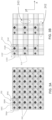
- FIG. 3A is a schematic diagram of a high-resolution portion of an emissive display having pixels 302 that include multiple light emitting elements and signal lines that supply electrical signals to the light emitting elements.
- FIG. 3B is a schematic diagram of a reduced-resolution portion of the emissive display having pixels 312 that include multiple light emitting elements and signal lines 242 that supply electrical signals to the light emitting elements.
- pixels 302, 312 in the display can include a plurality of light emitting elements (e.g., light emitting diodes) 306A, 306B, 306C, 316A, 316B, 316C that emit different colors, so that all visible colors can be produced by a pixel by mixing amount of light from the different elements.
- a pixel 302 can include a red LED 306A, a blue LED 306B and two green LEDs 306C.
- Electrical control signals and electrical power can be supplied to the light emitting elements 306A, 306B, 306C, 316A, 316B, 316C by electrically conductive signal lines 304, 314.
- the light emitting elements 306A, 306B, 306C, 316A, 316B, 316C and the signal lines 304, 314 can be opaque and/or can have an index of refraction that is not equal to 1, such that light is blocked by or diffracted by the elements and/or the signal lines and is propagates into or through the display.
- the reduced-resolution portion of the of the emissive display shown in FIG. 3B has a lower density per unit area of light emitting elements than the high-resolution portion of the emissive display shown in FIG. 3A
- the reduced-resolution portion may allow more light to pass through the display than the high-resolution portion of the display.
- the light passing through the display may still experience signal lines 242 running in a vertical (y) direction and/or in a horizontal (x) direction.
- FIG. 4 illustrates a schematic side, cross-sectional view of an emissive display 200 suitable for use with the mobile device of FIG. 1 .
- the display 200 can be an AMOLED display. While the principles of the disclosure may be applied to various other display technologies, the implementation of an AMOLED display will be considered throughout the disclosure.
- the emissive display 200 includes a plurality of layers. The layers are positioned behind (i.e., below) a cover glass layer 210 that can form the front surface of the mobile device 100.
- the display 200 can include a polarizer film layer 215.
- the display 200 can also include a touch sensor layer 220 that includes touch sensor electrodes 222.
- Pixels 237 for the display are formed from a cathode layer 230, an OLED emitter stack 235, and separate elements of an anode layer 236. Elements of the anode layer 236 may be reflective so that light is directed in a vertical (z) direction from the anode layer 236.
- An element of the anode layer 236 can be coupled to a thin film transistor (TFT) structure 240 that includes a source, a gate, and a drain, which can be controlled by electrical signals transmitted over signal lines 242.
- the display 200 can further include a barrier layer 245 of SiNx or SiONx and a substrate layer 250 of polyimide (PI).
- a metallic layer/film 410 for heat spreading and electrical shielding can be located below the display 200 to protect the display from localized hot spots due to heat-generating elements in the mobile device, such as, for example, a CPU, a GPU, etc., as well as from electrical signal noises from the underneath electrical components.
- the layers of the display 200 may include transparent and non-transparent circuit elements.
- the TFT structure 240, the pixels 237, the signal lines 242, and/or touch sensor electrodes 222 all may block light from propagating through the display 200.
- Light can be either reflected or absorbed by the non-transparent (i.e., opaque) circuit elements.
- the circuit elements may define gaps (i.e., periodic slits) with which the light may interact. For example, light may be diffracted by gaps formed between adjacent circuit elements in the same layer. Light may also be diffracted by gaps between circuit elements in different layers, although the effect may be weaker than the diffraction due to elements of the same layer.
- FIG. 5 is a schematic side, cross-sectional view of a portion of a display 200 with light diffracted by circuit elements in the display.
- a light ray 300A may pass between touch sensor electrodes 222A, 222B and between pixels 237A, 237B without being altered significantly.
- the light 300A can be diffracted by a gap formed between two adjacent signal lines 242A, 242B that are placed close to each other.
- the dimension of a gap relative to the wavelength of the light ray 300 can determine the effect the gap has on the light. Accordingly, light may diffracted by gaps formed by other combinations of circuit elements provided the gaps formed are of suitable dimensions.
- light 300B can be diffracted differently from by a gap formed between a signal line 242C and a TFT structure 240 than the light 300A that is diffracted by a gap between adjacent signal lines.
- a camera 502 positioned behind (i.e., below) the display 200 can image light, and an opening in the metallic layer/film 410 can allow light transmitted through the display to reach the camera.
- diffraction When light is considered as a collection of rays, diffraction may be understood as effectively changing angles of some of the rays in the collection of rays so that the diffracted rays 320A, 320B are distributed over a diffraction angle. In general, narrower gaps in the display result in larger diffraction angles. Accordingly, higher resolution displays may have more pronounced diffraction (i.e., larger diffraction angles) because the density of the control lines 242 in these displays is higher.
- the camera 502 relies on a lens to focus a light from an object onto a sensor (e.g., a CMOS, CCD array), with the sensor surface being located as the focal plane of the lens.
- a sensor e.g., a CMOS, CCD array
- many rays will not be focused onto the surface of the sensor but rather will have an effective focal plane above or below the sensor surface.
- an image captured from light that passes through a display can be distorted by diffraction.
- FIG. 6A depicts a simulated image of an object (i.e., a 3D model head) captured without diffraction
- FIG. 6B depicts a simulated image of a head captured with diffraction (i.e., through the display).
- the image formed with light including diffracted light is severely degraded and appears hazy because of the diffracted light rays.
- An aspect of the present disclosure is reducing diffraction caused by a display panel structure to improve the quality of images captured through the display (i.e., reduce a haze in the images).
- the present disclosure describes a display having a through-transmissive region 120 that, when positioned over (i.e., in front of) a camera, facilitates imaging by decreasing the amount of light that causes image distortion from reaching the camera 140. This may be partially accomplished by reducing a number of pixels in the through-transmissive region (see FIG. 3B ) (i.e., compared to other areas of the display) to allow more light to pass through the display.
- the pixels in the through-transmissive area may be regularly arranged (e.g., in a grid pattern) or may be non-regularly arranged.
- the number of pixels per unit area in the through-transmissive area may be smaller than that of the rest of display screen (e.g., the high-resolution area).
- the present disclosure describes additional modifications of the through-transmissive region (as compared to other regions) to increase throughput of light and decreased diffraction of the light.
- An additional modification includes a routing of signal lines between the pixels in a through-transmissive area of a display 120 in a manner designed to provide one or more relatively large areas with no, or relatively few, opaque and/or diffractive elements.
- FIGs. 7A and 7B depict example arrangements of pixels 712, 732 and signal lines 714, 718, 734, 738 of a through-transmissive area of a display.
- Each pixel in the through-transmissive area can include a plurality of sub-pixels, for example, a red sub-pixel 716A, 736A, green sub-pixels 716C, 736C, and a blue sub-pixel 716B, 736B, where the sub-pixels correspond to individual OLED emitters that can emit light of different colors.
- a pixel 712, 732 of the display that can emit light of any color can include three or more sub-pixels that emit light having at least three different colors, and the intensity of the different colors can be controlled, so that when mixed, the light from the multiple sub-pixels can produce light having any color.
- the sub-pixels 716A, 716B, 716C, 736A, 736B, 736C are addressed with signal lines 714, 718, 734, 738 that carry electrical signals to the sub-pixels to control their illumination.
- the pixels and their constituent sub-pixels are arranged in a repeating pattern in the display, and the pattern can be characterized by a unit cell 720, 740, which is a smallest geometric arrangement of the group of elements (i.e., pixels, their subpixels, and the signal lines that supply signal lines to the sub-pixels) that constitutes this repeating pattern of the structure.
- FIGs. 7A and 7B are top views of the structure, and that the unit cells 720, 740 are two-dimensional unit cells of elements that may not necessarily all lie in the same plane that is normal to a third dimension not represented in FIG. 7A or FIG. 7B .
- FIG. 7A is a schematic diagram of a reduced resolution portion of a display with signal lines in a conventional arrangement
- FIG. 7B is a schematic diagram of a reduced resolution portion of a display in which groups of signal lines that are rearranged to create relatively large openings 745 between the signal lines, where the openings 745 are free of sub-pixels and signal lines.
- the openings 745 provide substantially clear apertures through which light can pass to reach an optical device (or devices) positioned behind the display. In other words, the openings 745 are free of pixels or signal lines that could block or diffract light.
- the openings 745 may be contiguous areas within the unit area that are free from sub-pixels and signal lines.
- the unit cell may be referred to as a first area.
- the aperture may be referred to as a second area, and may be contained within the first area.
- FIG. 7B there are portions 742, 744 of a unit cell 740 between adjacent pixels 732 in which adjacent parallel signal lines 734, 738 are closer together than signal lines 714, 718 in counterpart portions 722, 724 shown in FIG. 7A .
- a group of parallel signal lines 714, 718 that supply control signals to subpixels of a pixel span a distance transverse to the signal lines that is comparable to the transverse extent of the subpixels of a pixel.
- FIG. 7A a group of parallel signal lines 714, 718 that supply control signals to subpixels of a pixel span a distance transverse to the signal lines that is comparable to the transverse extent of the subpixels of a pixel.
- a group of parallel signal lines 734 that supply control signals to subpixels 736A, 736B, 736C of a pixel 732 span a distance, d1, transverse to the signal lines 734 that is less than the transverse extent, h, in a first direction of the subpixels of the pixel.
- d1 can be less than 0.8*h, or less than 0.6*h, or less than 0.5*h, or less than 0.4*h.
- a group of signal lines 738 that are parallel to each other but that are not parallel to signal lines of group 734 and that supply control signals to the subpixels 736A, 736B, 736C of the pixel 732 span a distance, d2, transverse to the signal lines 738 that is less than the transverse extent, w, in a second direction of the subpixels of the pixel.
- d2 can be less an 0.8*h, or less than 0.6*h, or less than 0.5*h, or less than 0.4*h.
- the signal lines in the display can be arranged such that a unit cell 740 of the repeating pattern includes an open aperture 745 that is free of subpixels and signal lines, where the aperture 745 has an area that is greater than 40%, or greater than 60%, of the area of the unit cell 740.
- the signals lines in one or more of the portions 742, 744, in a group of three or more parallel signal lines, can be spaced apart from neighboring signal lines with a pitch (i.e., the distance the central axis of one signal line in the group to a central axis of a neighboring signal line) of less than 7 microns, or less than 6 microns, or less than 5 microns.
- a pitch i.e., the distance the central axis of one signal line in the group to a central axis of a neighboring signal line
- the signals lines in one or more of the portions 742, 744, in a group of two or more parallel signal lines, can be spaced apart from neighboring signal lines with a gap (i.e., the separation between an edge of one signal line in the group to an nearest edge of a neighboring signal line) or of less than one micron.
- the signals lines may have a width in a direction perpendicular to their central axis of greater than 500 nm.
- the circuit elements may form gaps (i.e., slits) that can diffract the light, and constraining the circuit elements (e.g., control signal lines) into bundled smaller regions (e.g., to create openings in the through-transmissive region) can enhance the diffraction, because the gaps are made smaller compared to a wavelength of light.
- the circuit elements e.g., control signal lines
- bundled smaller regions e.g., to create openings in the through-transmissive region
- an aspect of the disclosed display includes a light-blocking layer that has an opaque pattern aligned with the circuit elements in the through-transmissive area to block light before or after propagating through light-diffracting gaps formed by the circuit elements.
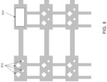
- FIG. 8 is a top view of an opaque pattern used in through-transmissive areas and configured to block light from passing through gaps between opaque elements in the display, to avoid diffraction of light by the gaps.
- the opaque pattern corresponds to a pattern of circuit elements (e.g., signal lines) of the portion of the display portion shown in FIG. 7 and is shaped and aligned accordingly.
- the opaque pattern may be made from a material (or materials) that have reflective or absorptive properties to all (or a portion) of the wavelengths of the light captured by the camera.
- the opaque pattern may be any thickness (e.g., the thickness of a deposited metal trace), but thin layers can offer additional flexibility and may reduce the effect of unwanted shadows.
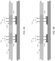
- FIG. 9A depicts a side, cross-sectional view of a reduced-resolution portion of an emissive display not forming part of the present invention, the display including an opaque layer above rearranged signal lines.
- the implementation in FIG 9A has fewer pixels, and the signals lines 242 are arranged to form openings 745 that do not include circuit elements, which light 820 can pass through without interacting with (e.g., being diffracted by) circuit elements.
- the lateral dimensions of an opening 745 can be greater than three times the longest wavelength of light that passes through the opening and that is imaged by a camera located below the display 200. By lateral dimensions, it is intended to refer to dimensions in directions parallel to the plane in which the display extends.
- the circuit elements can include control signal lines 242 and/or the TFT structure 240.
- the circuit elements are blocked (i.e., shaded) from receiving and diffracting light 810 by touch sensor electrodes 222.
- the touch sensor can be used as the light-blocking layer. This approach, rather than adding an additional light-blocking layer, may advantageously integrate with an existing fabrication processes.
- the pixel emission light 840 is unaffected by the opaque pattern formed by the touch sensor electrodes 222, because the touch sensor electrodes 222 are aligned with respect to the pixels, such that light from the pixels can be emitted from the display without inhibition from the touch sensor electrodes 222.
- a touch sensor in the through-transmissive area of the display may be active or inactive.
- the electrodes in the touch sensor layer 220 can include dummy sensor lines that do not contribute to sensing or active sensor lines used to detect a touch. Either the dummy or active sensor lines (or both) may be used to form an opaque pattern to block light from reaching the gaps created by the signal lines 242. That is, in addition to the active electrodes and sensor lines, the touch sensor layer 220 may be designed to include additional dummy sensor lines that, along with the active sensor lines, form an opaque pattern to block light from reaching the gaps created by the signal lines 242.
- an aspect of the disclosed display includes utilizing the touch sensor layer as a light-blocking layer by forming the electrode 222 for touch sensing into an opaque pattern to block (e.g., absorb, reflect) light 810 (e.g., visible and infrared light) that could otherwise be diffracted and degrade an image captured by a sensor located below the light blocking layer.
- the display implementation of FIG. 9A may advantageously have fewer layers because the touch sensor layer serves a dual purpose.
- FIG. 9B depicts another side, cross-sectional view of the reduced-resolution portion of an emissive display not forming part of the present invention.
- the touch sensor electrodes 222 are part of the touch sensor layer 220, and the touch sensor electrodes 222 can include an opaque metal material (e.g., Al, Ti, Mo, Cu, Cr, Ag, Au, etc. or alloys thereof). In some implementations, the thickness of the touch sensor electrodes 222 can be about 20 - 200 nm.
- the touch sensor layer 220 can be separated from the top cathode layer 230 of the OLED emitters 235 by a sensor buffer layer 225.
- the sensor buffer layer can include, for example, SiN or SiON material.
- the touch sensor electrodes 222 include metal material, the reflectivity of the metal material may be relatively high. To reduce the reflectivity of the touch sensor electrodes 222, the electrodes may be covered with a layer of low reflectivity material.
- the metal touch sensor electrodes 222 can be covered by an additional optically absorbing material 224 that covers the surface of touch sensor electrodes 222.
- the optically absorbing material 224 can extend around the edges of the electrodes to cover the edges of the metal touch sensor electrodes 222.
- the optically absorbing material 224 can include a black photoresist material, which can be similar in composition to materials used for LCD color filter fabrication and which is typically modified for low temperature curing necessary for compatibility with OLEDs (e.g.
- the total combined thickness of the touch sensor electrodes 222 covered by an optically absorbing material 224 can be about 200 - 500 nm.
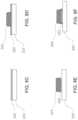
- FIGS. 9C, 9D, 9E, and 9F depict side, cross-sectional views of a metal touch sensor electrode 222 in various stages of being covered by an opaque, low-reflectivity material.
- FIG. 9C depicts a side cross-sectional view of a metal touch sensitive electrode layer 222 on a supporting substrate layer 223.
- FIG. 9D depicts a side cross-sectional view of a metal touch sensitive electrode layer 222 on a supporting substrate layer 223, with a photoresist layer 224 above the metal layer 222.
- the photoresist layer 224 can be patterned with conventional photolithography techniques (e.g., coating the underlying metal layer 222 with a photoresist layer spanning the substrate layer 223, exposing the photoresist layer to a pattern of light, developing the exposed photoresist layer, baking the layer) to create the pattern of photoresist depicted in FIG. 9D .
- the photoresist layer typically can be about 1 - 3 ⁇ m thick.
- a metal etching process can be applied to the stack shown in FIG. 9D to remove material from the metal layer 222 that is not directly under the patterned photoresist layer 224.
- FIG. 9E depicts a side cross-sectional view of the metal touch sensitive electrode layer 222 on the supporting substrate layer 223, with a photoresist layer 224 above the metal layer 222, after metal etching has been applied to remove metal from layer 222, except under patterned resist 224.
- the metal layer can be overetched, so that the photoresist layer 224 extends outward, parallel to the substrate layer beyond the edges of the remaining metal electrode layer 222.
- the structure shown in FIG. 9E can be further processed, so that the photoresist layer 224, covers the edges of the metal layer 222.
- the structure shown in FIG. 9E can be heated, so that the photoresist 224 flows down over the edges of the metal layer 222 to form the structure shown in FIG. 9F .
- a touch sensor layer 220 for an emissive display may itself include multiple layers.
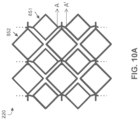
- FIG. 10A depicts a top view of electrodes in the touch sensor layer 220.
- the electrodes include a transmit (TX) sensor electrode 851 and a receive (RX) sensor electrode 852.
- FIG. 10B depicts a side, cross-sectional view of a portion (shown as A-A') of the touch sensor layers of FIG. 10A .
- the TX sensor electrode 851 and the RX sensor electrode 852 are coplanar and occupy a first metal layer 850.
- the TX and RX electrodes form overlapping patterns.
- a second metal layer 860 is used for a jumper (i.e., bridge) electrode 861 to allow the overlapping electrical connections.
- the touch sensor layer 220 may further include a sensor passivation layer 870 and a sensor buffer layer 880.
- the opaque pattern of the touch sensor electrode for blocking light may include either, or both, the first metal layer 850 and the second metal layer 860 of the touch sensor layer 220.
- the electrodes 222 shown in FIG. 9A may be generally regarded as being a part of a first metal layer 850 or as part of a second metal layer 860 of the touch sensor layer 220.
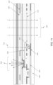
- FIG. 11 depicts a side, cross-sectional view of a reduced-resolution portion of an emissive display including an opaque layer below signal lines according to the present invention.
- the display can include an opaque pattern 930 on the substrate (e.g., polyimide layer) 250 for blocking light.
- the opaque pattern 930 on the substrate 250 can include, for example, metal, photoresist, polymer, and other opaque materials.
- the opaque pattern 930 is positioned below and aligned with the circuit elements (e.g., signal lines 242) that can cause deleterious diffraction of light 910 passing through gaps between the elements, resulting in diffracted light 940.
- the diffracted light 940 can be blocked by the opaque pattern 930 on the substrate layer 250.
- the opaque pattern 930 of the light blocking layer being below the OLEDs of the pixels, apertures in the opaque layer for transmitted light 840 from pixels to shine through are unnecessary. Accordingly, the precision of alignment of the opaque mask with respect to the OLEDs may be relaxed somewhat compared to implementations requiring apertures for the OLEDs. As shown in FIG. 11 , the spacing between the opaque pattern 930 and the circuit elements (e.g., signal lines 242) is made small enough that diffracted light 940 is blocked before it can reach an opening 510.
- layers may be added to the display with the sole purpose of blocking light.
- layers other than the layers described thus far may be adapted to serve a dual purpose that includes blocking light.
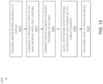
- FIG. 12 is a flowchart of a method for imaging through a display according to an implementation of the present disclosure.
- the method 1000 begins with positioning 1010 a camera behind an area (i.e., a through-transmissive area). A portion of the pixels in the area are eliminated 1020 to increase the inter-pixel spacing. The increased inter-pixel spacing allows the display to remain active (e.g., in a display mode) while blocking less of the area for receiving light directed to the area (i.e., incident) light (e.g., in an imaging mode).
- the circuit elements in the area are then arranged 1030 to define openings in the area for light to easily pass through without encountering (e.g., being blocked, diffracted, reflected, or otherwise redirected by) pixels or circuit elements.
- the circuit elements may be control signal lines for the pixels in the TFT layer of the display.
- the control signal lines can be arranged by forming closely spaced groups that are aligned between pixels.
- a first portion of the light directed to the area of the display can pass through the display without encountering any of the circuit elements.
- a second portion of the light directed to the display can be diffracted by gaps formed by the circuit elements. Unless this second portion is blocked or prevented from forming, the diffracted light could degrade an image captured by the camera.
- the method includes blocking 1040 the second portion of the light directed to the area of the display using a light-blocking layer before or after the second portion of light is diffracted through gaps formed by the circuit elements.
- the first portion of light is captured by the camera (i.e., by a lens of the camera) and an image is captured 1050 (e.g., formed on an array of light sensors and reconstructed digitally based on the response from each sensor).
- Variations to the method described in FIG. 12 may exist. For example, while blocking diffracted light from reaching a camera to improve the quality of an image captured by the camera has been described, the disclosed principles and techniques may be applied to other applications. For example, the performance of a light sensor used for detecting ambient light may be improved by one or more steps (or variations thereof) of the disclosed method. Additionally, the disclosed principles and techniques may be applied to a light source rather than a light sensor. For example, the performance of an illuminator may be improved by one or more steps (or variations thereof) in the disclosed method.
- a light source e.g. an illuminator
- a light sensor e.g. a camera
- steps 1010, 1020, 1030, 1040 may be performed during the design and/or manufacture process of a device, whereas the step 1050 may be performed at a later time by a user of the device.
- the steps may be performed in a different order to that described.
- steps 1020, 1030 and/or 1040 may be performed as part of a fabrication process, before a camera is physically positioned adjacent to the display during a assembly process.
- Steps 1010, 1020, 1030 and/or 1040 may be performed as part of a design process. For example, it may be that no pixels are physically eliminated in step 1020.
- step 1010 may refer to a camera (or other light sensor, or a light source) being positioned behind the display in a design process, rather than being physically positioned.
- the disclosed displays have been presented in the context of a mobile device, such as a tablet or a smart phone.
- a virtual agent home terminal, a television, or an automatic teller machine (ATM) are a non-limiting set of alternative applications that could utilize a camera positioned behind an active area of a display.
- ATM automatic teller machine
- the motivation for placing a camera behind a display is not limited to an expansion of the display to the edges of a device. For example, it may be desirable to place the camera behind a display for aesthetic or stealth reasons.
- a "front surface” of a mobile computing device may be a surface facing a user, in which case the phrase “in front of” implies closer to the user.
- a "top surface” of a display may be the surface facing a user, in which case the phrase “below” implies deeper into an interior of the mobile computing device, and the phrase “above” implies closer to the surface of the display facing the user.
Landscapes
- Engineering & Computer Science (AREA)
- Microelectronics & Electronic Packaging (AREA)
- Chemical & Material Sciences (AREA)
- Inorganic Chemistry (AREA)
- Sustainable Development (AREA)
- Life Sciences & Earth Sciences (AREA)
- Physics & Mathematics (AREA)
- General Engineering & Computer Science (AREA)
- Theoretical Computer Science (AREA)
- Geometry (AREA)
- Human Computer Interaction (AREA)
- General Physics & Mathematics (AREA)
- Devices For Indicating Variable Information By Combining Individual Elements (AREA)
- Manufacturing & Machinery (AREA)
- Signal Processing (AREA)
- Electroluminescent Light Sources (AREA)
Description
- This application is a Nonprovisional of, and claims priority to,
U.S. Provisional Patent Application No. 62/853,044, filed on May 26, 2019 - The present disclosure relates to flat panel displays and more specifically to a display for a mobile device that enables imaging through the display.
- Expanding a display to cover more area of a mobile device (e.g., mobile phone, tablet, etc.) may be desirable from, at least, a user experience standpoint. However, electro-optical devices positioned on a side of the mobile device that also includes the display (e.g., a front-facing camera, a light sensor, an emissive status light, etc.) may compete for real estate on the side of the device that includes the display. Thus, the size of the emissive area of the display may have to be compromised to accommodate the electro-optical devices on the display side of the device.
CN 108 269 840 relates to a display screen.US 2011/102308 relates to an image display unit having an imaging unit disposed at its rear side.US 2019/16097 relates to a display apparatus having a touch panel.CN 109 192 759 relates to a display panel having a plurality of transparent portions.WO 2019/199693 relates to through-display imaging.US 2018/182816 relates to a display device with an integrated touch screen. - The present invention is defined in independent claim 1. Further aspects of the invention are defined in the dependent claims.
- In another general aspect, the disclosure describes a method for imaging through a display. The method includes positioning a camera behind an area of a display to receive light directed to the area. The method further includes eliminating a portion of pixels in the area so that the pixels in the area are spaced further apart than outside the area. Next, circuit elements in the area are arranged to create openings in the area so that a first portion of the light directed to the area can pass through without encountering any of the circuit elements. Next, a second portion of the light directed to the area is blocked using a wider opaque layer before or after the second portion of light is diffracted by gaps formed by the circuit elements. Finally, using the camera, the first portion of the light is captured to create an image.
- In another general aspect, the disclosure describes a mobile computing device comprising a display having a high-resolution area and a through-transmissive area. The through-transmissive area includes pixels that are spaced in a repeating pattern according to a first pixel density that is lower than a second pixel density of the high-resolution area. The through-transmissive area further includes circuit elements configured to control the pixels, and a light-blocking layer having an opaque pattern that is aligned with the circuit elements to block light before or after propagating through gaps formed by the circuit elements. The mobile computing device further comprises a light device positioned behind the through-transmissive area, such that the circuit elements and the light-blocking layer are between a surface of the display and the light device, wherein the light device is configured to receive or transmit light through the display that is not blocked by the light-blocking layer.
- Where the light device is a sensor, the sensor may be configured to receive light through the display that is not blocked by the light-blocking layer. Where the light device is a light source, the light source may be configured to transmit light through the display that is not blocked by the light-blocking layer.
- The display may include an active matrix organic light emitting diode (AMOLED) display.
- The circuit elements may include signal lines. In a repeating pattern of pixels in the through-transmissive area, in a group of three or more parallel signal lines between adjacent pixels, adjacent signal lines may be spaced apart from each other by less than 7 microns.
- The circuit elements may include signal lines. In a repeating pattern of pixels in the through-transmissive area, in a group of three or more parallel signal lines between adjacent pixels, adjacent signal lines may be spaced apart from each other by less than 5 microns.
- The circuit elements may include signal lines. The repeating pattern of pixels may be characterized by a unit cell having a first area. The unit cell may include a second area that is free of subpixels and free of signal lines and that is greater than 40% of the first area.
- The opaque pattern may absorb visible and infrared light.
- The opaque pattern may reflect visible and infrared light.
- The light device may comprise a light sensor.
- The light sensor may include a camera.
- The through-transmissive region does have a pixel density that is lower than other regions of the active pixel area and does include circuit elements arranged such that they diffract visible light that passes through the through-transmissive region.
- The light-blocking layer does include a pattern of opaque portions and transparent portions. The opaque portions are positioned below, and aligned with, the circuit elements to prevent light transmitted through the through transmissive region and diffracted by the circuit elements from reaching the light device.
- The circuit elements in the through-transmissive region may include signal lines configured to provide electrical signals to pixels in the display.
- A width of the signal lines may be greater than 500 nm.
- Two or more of the signal lines may be are parallel to each other, with a gap between the parallel signal lines being less than one micron.
- The foregoing illustrative summary, as well as other exemplary objectives and/or advantages of the disclosure, and the manner in which the same are accomplished, are further explained within the following detailed description and its accompanying drawings.
-
-
FIG. 1A depicts a top (front) surface of a mobile computing device including a display and an optical device that occupy different portions of the front surface. -
FIG. 1B depicts a top (front) surface of a mobile computing device including a display with an optical device positioned behind a through-transmissive area of the display according to a possible implementation of the disclosure. -
FIG. 1C depicts a top (front) surface of a mobile computing device including a display with an optical device position behind a through-transmissive area of the display according to a possible implementation of the disclosure. -
FIG. 2A depicts a side, cross-sectional view of a mobile device that may include a plurality of optical devices, each positioned behind a respective through-transmissive area of an emissive display according to a possible implementation of the disclosure. -
FIG. 2B depicts a side, cross-sectional view of a mobile device that may include a plurality of optical devices positioned behind a single through-transmissive area of an emissive display according to a possible implementation of the disclosure. -
FIG. 2C is a schematic diagram of a display system that includes a display panel having emissive pixels that include subpixels that are controlled by electronic pixel circuits and/or subpixel circuits to render a visual output. -
FIG. 3A depicts a top (front) view of pixels and signal lines of a high-resolution portion of an emissive display according to a possible implementation of the disclosure. -
FIG. 3B depicts a top (front) view of pixels and signal lines of a reduced-resolution portion of an emissive display according to a possible implementation of the disclosure. -
FIG. 4 depicts a possible side, cross-sectional view of the emissive display shown inFIG. 3B . -
FIG. 5 depicts the possible effects on light passing through the emissive display ofFIG. 4 . -
FIG. 6A depicts an example of an image captured from light without diffraction. -
FIG. 6B depicts an example of an image captured from light with diffraction. -
FIG. 7A is a schematic diagram of a reduced resolution portion of a display. -
FIG. 7B depicts a possible rearrangement of signal lines of the reduced-resolution portion of an emissive display to produce clear apertures for light to pass through. -
FIG. 8 is a top (front) view of an opaque pattern for preventing light from reaching the rearranged signal lines ofFIG. 7B while allowing light from pixels of the emissive display to transmit through. -
FIG. 9A depicts a side, cross-sectional view of a reduced-resolution portion of an emissive display not forming part of the present invention, the display including an opaque layer above rearranged signal lines according to a possible implementation of the disclosure. -
FIG. 9B depicts another side, cross-sectional view of a reduced-resolution portion of an emissive display not forming part of the present invention, the display including an opaque layer above rearranged signal lines according to a possible implementation of the disclosure. -
FIGS. 9C, 9D, 9E, and 9F depict side, cross-sectional views of a metal touch sensor electrode in various stages of being covered by an opaque, low-reflectivity material. -
FIG. 10A depicts a top view of electrodes in touch sensor layers. -
FIG. 10B depicts a side, cross-sectional view of a portion (A-A') of the touch sensor layers ofFIG. 10A . -
FIG. 11 depicts a side, cross-sectional view of a reduced-resolution portion of an emissive display including an opaque layer below rearranged signal lines according to the present invention. -
FIG. 12 depicts a flowchart of a method for imaging through a display according to an implementation of the present disclosure. - The components in the drawings are not necessarily drawn to scale and may not be in scale relative to each other. Like reference numerals designate corresponding parts throughout the several views.
- The present disclosure describes a flat panel display (i.e., display) that can be used with a mobile device (e.g., mobile phone, tablet, etc.). The front surface of a mobile device includes a display typically operating as a graphic user interface (GUI) and one or more optical devices operating as sensors or emitters. The one or more optical devices can be configured for a variety of functions, including sensing lighting conditions (e.g. a light sensor), sensing proximity (e.g., an electromagnetic sensor), capturing images (e.g., a front-facing camera), and/or to providing light (e.g., flash). An optical device can be located under a portion of the display, such that display area need not be sacrificed to accommodate the optical device on the front surface of the mobile device. Circuitry and optical masks within the mobile device can be arranged, such that diffraction of light passing through the display to or from the optical device is reduced compared to conventional configurations of mobile devices.
- Traditionally, the emissive portion of the display and the optical devices have occupied separate areas of the front surface of the mobile device. For example,
FIG. 1A depicts amobile device 101 having adisplay 110 and acamera 111 that occupy different portions of the front surface. Recent advances in emissive display technology (e.g., active matrix organic light emitting diode (AMOLED)) facilitate extending the emissive (i.e., active) area of the display towards the edges of the mobile device. By extending the active area of the display towards the edges of the mobile device, a user may experience the benefits of a larger display without the drawbacks of a larger form factor device. - The disclosed emissive display is configured to share the front surface of a mobile device with one or more optical devices so that the active area of the display can be extended to the edges, without the need for leaving gaps in the display of a bezel around the display in which to locate the optical devices. Accordingly, one or more portions of the disclosed display covering the one or more optical devices can be configured so that the optical devices, positioned behind the display, can transmit or receive radiation (e.g., light) through the display.
-
FIG. 1B illustrates amobile device 102 with adisplay 112 extended towards the edges of the device. Unlike mobile devices in which the display is excluded from an area reserved for optical devices, the light-emitting (i.e., active) area of thedisplay 112 extends over substantially the entire front surface of thedevice 102. Accordingly, nearly the entire front surface of themobile device 102 may be used to present color, black-and-white, or gray-scale images, graphics, and/or characters. Thedisplay 112 includes one or more through-transmissive areas 120 behind which (i.e., below which) an optical device (or optical devices) may be disposed and through which light can be transmitted to be received by the optical device and/or through which light can be transmitted from the optical device and out of thedisplay 112. - The size, shape, and/or position of the through-
transmissive area 120 may be implemented variously. For example, as shown inFIG. 1B , the through-transmissive area 120 can have a rounded (e.g., circular) shape and can be positioned within a perimeter of thedisplay 112 and spaced apart from edges of thedisplay 112, but other shapes and locations of the through-transmissive area 120 are possible. For example, as shown inFIG. 1C , a through-transmissive area 120 can have rectangular in shape and can be positioned along an edge of thedisplay 112. In this implementation, the horizontal and vertical edges of the through-transmissive area 120 can correspond to the horizontal and vertical directions of a grid arrangement of light-emitting pixels in thedisplay 112 and to the horizonal and vertical directions of electrical signal lines signal lines that deliver electrical signals to the pixels. Additionally, the size of the through-transmissive region 120 inFIG. 1C can be different than that size of the through-transmissive area inFIG. 1B . -
FIG. 2A depicts a side, cross-sectional view of a mobile device having adisplay 112 with multiple through-transmissive regions 120A, 120B though which electromagnetic radiation can be transmitted to or from an optical device located under the display, for example, a camera located under the display. The mobile device can include multipleoptical devices 140A, 140B, each positioned behind different through-transmissive areas 120A, 120B.FIG. 2B depicts a side, cross-sectional view of a mobile device having adisplay 112 with a single region 120C for use by the multipleoptical devices 140A, 140B. - The
optical devices 140A, 140B may transmit and/or receiveelectromagnetic radiation 125 through the through-transmissive regions 120A, 120B, 120C. While the disclosure may be generally applied to any optical device configured to transmit or receive electromagnetic radiation (e.g., from the millimeter wave, visible, or infrared portions of the electromagnetic spectrum), the particular implementation of a camera configured to receive visible light and/or infrared light will be considered throughout the disclosure. - In some implementations, pixels in the through-transmissive areas 120A, 120B, 120C of the
display 112 through which light passes to an underlying sensor may have the same pixel density and/or pixel arrangement as in the rest of the display. In some implementations, the through-transmissive areas 120A, 120B, 120C (i.e., portion) of thedisplay 112 through which light passes to an underlying sensor may have a different pixel density and/or pixel arrangement than the rest of the display. For example, in some implementations, the display region of the rest of the display may have a pixel density that is higher than the pixel density in the through-transmissive areas 120A, 120B, 120C, such that the resolution of the display (e.g., as measured in pixels per inch (ppi)) is lower in the through-transmissive areas 120A, 120B, 120C than in the rest of the display. -
FIG. 2C schematically depicts a possible display system 260 that can be used with amobile device 102 ofFIG. 1B or FIG. 1C . The display system 260 includes a display panel 262 having emissive pixels that include subpixels that are controlled by electronic pixel circuits and/or subpixel circuits to render a visual output (e.g., text, graphics, video, images, etc.) on the display. A subpixel can be considered as an individual light emitting element, generally having a monochromatic light output, whereas a pixel can be considered as a combination of two or more light emitting elements, where the different light emitting elements have different colors, so the pixel can be controlled to output a range of colors. The display may be any active matrix display, such as an active matrix organic light emitting diode (AMOLED) display. - A magnified portion 270 of the display panel 262 is shown. The magnified portion 270 illustrates the row/column configuration of subpixels 272. The light emission of each subpixel 272 can be controlled by a scan (gate) signal line 274 (i.e., a horizontal control line) and by a column data line 276 (i.e., a vertical control line). In some implementations, and as illustrated in
FIG. 2 , all subpixels in a row share can be driven by the same gate signal line, and all subpixels in a column can be driven by the same column data line. - The scan signal lines 274 of the display panel 262 are controlled by gate drivers 280. The column data lines are controlled by
column line drivers 282. Each column data line 276 may have a panel switch in series for switching (e.g., demultiplexing) data voltages from the column line driver 282 (e.g., to control the intensity of a pixel). A timing controller 284 can control signals to the scan line drivers 280 and to thecolumn line drivers 282 to ensure proper timing of signals to individual subpixels to achieve a desired light emission from the subpixels. The timing controller 284 can receive control signals from a system-on-a-chip 286 that includes, for example, a central processing unit (CPU). -
FIG. 3A is a schematic diagram of a high-resolution portion of an emissivedisplay having pixels 302 that include multiple light emitting elements and signal lines that supply electrical signals to the light emitting elements.FIG. 3B is a schematic diagram of a reduced-resolution portion of the emissivedisplay having pixels 312 that include multiple light emitting elements andsignal lines 242 that supply electrical signals to the light emitting elements. InFIG. 3A and inFIG. 3B ,pixels pixel 302 can include ared LED 306A, a blue LED 306B and twogreen LEDs 306C. Electrical control signals and electrical power can be supplied to thelight emitting elements conductive signal lines light emitting elements signal lines FIG. 3B has a lower density per unit area of light emitting elements than the high-resolution portion of the emissive display shown inFIG. 3A , the reduced-resolution portion may allow more light to pass through the display than the high-resolution portion of the display. However, the light passing through the display may still experiencesignal lines 242 running in a vertical (y) direction and/or in a horizontal (x) direction. -
FIG. 4 illustrates a schematic side, cross-sectional view of anemissive display 200 suitable for use with the mobile device ofFIG. 1 . In some implementations thedisplay 200 can be an AMOLED display. While the principles of the disclosure may be applied to various other display technologies, the implementation of an AMOLED display will be considered throughout the disclosure. - As shown in
FIG. 4 , theemissive display 200 includes a plurality of layers. The layers are positioned behind (i.e., below) acover glass layer 210 that can form the front surface of the mobile device 100. In a possible implementation, thedisplay 200 can include apolarizer film layer 215. Thedisplay 200 can also include atouch sensor layer 220 that includestouch sensor electrodes 222.Pixels 237 for the display are formed from acathode layer 230, anOLED emitter stack 235, and separate elements of ananode layer 236. Elements of theanode layer 236 may be reflective so that light is directed in a vertical (z) direction from theanode layer 236. An element of theanode layer 236 can be coupled to a thin film transistor (TFT)structure 240 that includes a source, a gate, and a drain, which can be controlled by electrical signals transmitted over signal lines 242. Thedisplay 200 can further include abarrier layer 245 of SiNx or SiONx and asubstrate layer 250 of polyimide (PI). A metallic layer/film 410 for heat spreading and electrical shielding can be located below thedisplay 200 to protect the display from localized hot spots due to heat-generating elements in the mobile device, such as, for example, a CPU, a GPU, etc., as well as from electrical signal noises from the underneath electrical components. - The layers of the
display 200 may include transparent and non-transparent circuit elements. For example, theTFT structure 240, thepixels 237, thesignal lines 242, and/ortouch sensor electrodes 222 all may block light from propagating through thedisplay 200. Light can be either reflected or absorbed by the non-transparent (i.e., opaque) circuit elements. Additionally, the circuit elements may define gaps (i.e., periodic slits) with which the light may interact. For example, light may be diffracted by gaps formed between adjacent circuit elements in the same layer. Light may also be diffracted by gaps between circuit elements in different layers, although the effect may be weaker than the diffraction due to elements of the same layer. -
FIG. 5 is a schematic side, cross-sectional view of a portion of adisplay 200 with light diffracted by circuit elements in the display. As shown, alight ray 300A may pass betweentouch sensor electrodes pixels 237A, 237B without being altered significantly. However, thelight 300A can be diffracted by a gap formed between two adjacent signal lines 242A, 242B that are placed close to each other. The dimension of a gap relative to the wavelength of the light ray 300 can determine the effect the gap has on the light. Accordingly, light may diffracted by gaps formed by other combinations of circuit elements provided the gaps formed are of suitable dimensions. For example, light 300B can be diffracted differently from by a gap formed between a signal line 242C and aTFT structure 240 than the light 300A that is diffracted by a gap between adjacent signal lines. A camera 502 positioned behind (i.e., below) thedisplay 200 can image light, and an opening in the metallic layer/film 410 can allow light transmitted through the display to reach the camera. - When light is considered as a collection of rays, diffraction may be understood as effectively changing angles of some of the rays in the collection of rays so that the diffracted
rays control lines 242 in these displays is higher. - The camera 502 relies on a lens to focus a light from an object onto a sensor (e.g., a CMOS, CCD array), with the sensor surface being located as the focal plane of the lens. However, when the light rays that pass through the display to the lens are diffracted by opaque elements in the display, many rays will not be focused onto the surface of the sensor but rather will have an effective focal plane above or below the sensor surface. As a result, an image captured from light that passes through a display can be distorted by diffraction.
-
FIG. 6A depicts a simulated image of an object (i.e., a 3D model head) captured without diffraction, andFIG. 6B depicts a simulated image of a head captured with diffraction (i.e., through the display). As shown, the image formed with light including diffracted light is severely degraded and appears hazy because of the diffracted light rays. An aspect of the present disclosure is reducing diffraction caused by a display panel structure to improve the quality of images captured through the display (i.e., reduce a haze in the images). - The present disclosure describes a display having a through-
transmissive region 120 that, when positioned over (i.e., in front of) a camera, facilitates imaging by decreasing the amount of light that causes image distortion from reaching the camera 140. This may be partially accomplished by reducing a number of pixels in the through-transmissive region (seeFIG. 3B ) (i.e., compared to other areas of the display) to allow more light to pass through the display. The pixels in the through-transmissive area may be regularly arranged (e.g., in a grid pattern) or may be non-regularly arranged. The number of pixels per unit area in the through-transmissive area may be smaller than that of the rest of display screen (e.g., the high-resolution area). In other words, a portion of pixels in the through-transmissive area can eliminated so that the remaining pixels are spaced further apart than the pixels of other parts of the display. This approach alone may still permit light to diffract from gaps formed between circuit elements (e.g., signal lines 242). Accordingly, the present disclosure describes additional modifications of the through-transmissive region (as compared to other regions) to increase throughput of light and decreased diffraction of the light. - An additional modification includes a routing of signal lines between the pixels in a through-transmissive area of a
display 120 in a manner designed to provide one or more relatively large areas with no, or relatively few, opaque and/or diffractive elements.FIGs. 7A and7B depict example arrangements ofpixels signal lines red sub-pixel pixel signal lines unit cell FIGs. 7A and7B are top views of the structure, and that theunit cells FIG. 7A orFIG. 7B . -
FIG. 7A is a schematic diagram of a reduced resolution portion of a display with signal lines in a conventional arrangement, whileFIG. 7B is a schematic diagram of a reduced resolution portion of a display in which groups of signal lines that are rearranged to create relativelylarge openings 745 between the signal lines, where theopenings 745 are free of sub-pixels and signal lines. Theopenings 745 provide substantially clear apertures through which light can pass to reach an optical device (or devices) positioned behind the display. In other words, theopenings 745 are free of pixels or signal lines that could block or diffract light. Theopenings 745 may be contiguous areas within the unit area that are free from sub-pixels and signal lines. The unit cell may be referred to as a first area. The aperture may be referred to as a second area, and may be contained within the first area. - As shown in
FIG. 7B , there areportions unit cell 740 betweenadjacent pixels 732 in which adjacentparallel signal lines signal lines counterpart portions FIG. 7A . In particular, inFIG. 7A , a group ofparallel signal lines FIG. 7B , a group ofparallel signal lines 734 that supply control signals tosubpixels 736A, 736B, 736C of apixel 732 span a distance, d1, transverse to thesignal lines 734 that is less than the transverse extent, h, in a first direction of the subpixels of the pixel. For example, d1 can be less than 0.8*h, or less than 0.6*h, or less than 0.5*h, or less than 0.4*h. Similarly, a group ofsignal lines 738 that are parallel to each other but that are not parallel to signal lines ofgroup 734 and that supply control signals to thesubpixels 736A, 736B, 736C of thepixel 732 span a distance, d2, transverse to thesignal lines 738 that is less than the transverse extent, w, in a second direction of the subpixels of the pixel. For example, d2 can be less an 0.8*h, or less than 0.6*h, or less than 0.5*h, or less than 0.4*h. - In some implementations, as shown in
FIG. 7B , the signal lines in the display can be arranged such that aunit cell 740 of the repeating pattern includes anopen aperture 745 that is free of subpixels and signal lines, where theaperture 745 has an area that is greater than 40%, or greater than 60%, of the area of theunit cell 740. - In some implementations, in one or more of the
portions - In some implementations, in one or more of the
portions - As mentioned, the circuit elements may form gaps (i.e., slits) that can diffract the light, and constraining the circuit elements (e.g., control signal lines) into bundled smaller regions (e.g., to create openings in the through-transmissive region) can enhance the diffraction, because the gaps are made smaller compared to a wavelength of light. However, to prevent diffracted light from reaching the camera, light directed to circuit elements of the display that would cause deleterious diffraction can be blocked before reaching the circuit elements or after being diffracted by the circuit elements but before reaching the camera (i.e., after passing through the circuit elements). Accordingly, an aspect of the disclosed display includes a light-blocking layer that has an opaque pattern aligned with the circuit elements in the through-transmissive area to block light before or after propagating through light-diffracting gaps formed by the circuit elements.
-
FIG. 8 is a top view of an opaque pattern used in through-transmissive areas and configured to block light from passing through gaps between opaque elements in the display, to avoid diffraction of light by the gaps. The opaque pattern corresponds to a pattern of circuit elements (e.g., signal lines) of the portion of the display portion shown inFIG. 7 and is shaped and aligned accordingly. The opaque pattern may be made from a material (or materials) that have reflective or absorptive properties to all (or a portion) of the wavelengths of the light captured by the camera. The opaque pattern may be any thickness (e.g., the thickness of a deposited metal trace), but thin layers can offer additional flexibility and may reduce the effect of unwanted shadows. -
FIG. 9A depicts a side, cross-sectional view of a reduced-resolution portion of an emissive display not forming part of the present invention, the display including an opaque layer above rearranged signal lines. Compared withFIG. 4 , the implementation inFIG 9A has fewer pixels, and thesignals lines 242 are arranged to formopenings 745 that do not include circuit elements, which light 820 can pass through without interacting with (e.g., being diffracted by) circuit elements. The lateral dimensions of anopening 745 can be greater than three times the longest wavelength of light that passes through the opening and that is imaged by a camera located below thedisplay 200. By lateral dimensions, it is intended to refer to dimensions in directions parallel to the plane in which the display extends. The circuit elements can includecontrol signal lines 242 and/or theTFT structure 240. The circuit elements are blocked (i.e., shaded) from receiving and diffracting light 810 bytouch sensor electrodes 222. In other words, the touch sensor can be used as the light-blocking layer. This approach, rather than adding an additional light-blocking layer, may advantageously integrate with an existing fabrication processes. Thepixel emission light 840 is unaffected by the opaque pattern formed by thetouch sensor electrodes 222, because thetouch sensor electrodes 222 are aligned with respect to the pixels, such that light from the pixels can be emitted from the display without inhibition from thetouch sensor electrodes 222. - A touch sensor in the through-transmissive area of the display may be active or inactive. For example, the electrodes in the
touch sensor layer 220 can include dummy sensor lines that do not contribute to sensing or active sensor lines used to detect a touch. Either the dummy or active sensor lines (or both) may be used to form an opaque pattern to block light from reaching the gaps created by the signal lines 242. That is, in addition to the active electrodes and sensor lines, thetouch sensor layer 220 may be designed to include additional dummy sensor lines that, along with the active sensor lines, form an opaque pattern to block light from reaching the gaps created by the signal lines 242. Thus, an aspect of the disclosed display includes utilizing the touch sensor layer as a light-blocking layer by forming theelectrode 222 for touch sensing into an opaque pattern to block (e.g., absorb, reflect) light 810 (e.g., visible and infrared light) that could otherwise be diffracted and degrade an image captured by a sensor located below the light blocking layer. The display implementation ofFIG. 9A may advantageously have fewer layers because the touch sensor layer serves a dual purpose. -
FIG. 9B depicts another side, cross-sectional view of the reduced-resolution portion of an emissive display not forming part of the present invention. Thetouch sensor electrodes 222 are part of thetouch sensor layer 220, and thetouch sensor electrodes 222 can include an opaque metal material (e.g., Al, Ti, Mo, Cu, Cr, Ag, Au, etc. or alloys thereof). In some implementations, the thickness of thetouch sensor electrodes 222 can be about 20 - 200 nm. Thetouch sensor layer 220 can be separated from thetop cathode layer 230 of theOLED emitters 235 by asensor buffer layer 225. The sensor buffer layer can include, for example, SiN or SiON material. - Because the
touch sensor electrodes 222 include metal material, the reflectivity of the metal material may be relatively high. To reduce the reflectivity of thetouch sensor electrodes 222, the electrodes may be covered with a layer of low reflectivity material. For example, in some implementations, the metaltouch sensor electrodes 222 can be covered by an additional optically absorbingmaterial 224 that covers the surface oftouch sensor electrodes 222. In some embodiments, the optically absorbingmaterial 224 can extend around the edges of the electrodes to cover the edges of the metaltouch sensor electrodes 222. For example, the optically absorbingmaterial 224 can include a black photoresist material, which can be similar in composition to materials used for LCD color filter fabrication and which is typically modified for low temperature curing necessary for compatibility with OLEDs (e.g. 100-120 °C). These materials have high optical absorption for optical wavelengths of light (e.g. > 90% for 1 µm thickness layer of photoresist) and can help decrease the amount of light scattered by metaltouch sensor electrodes 222 towards the imaging device behind the display panel. In some implementations, the total combined thickness of thetouch sensor electrodes 222 covered by an optically absorbingmaterial 224 can be about 200 - 500 nm. -
FIGS. 9C, 9D, 9E, and 9F depict side, cross-sectional views of a metaltouch sensor electrode 222 in various stages of being covered by an opaque, low-reflectivity material.FIG. 9C depicts a side cross-sectional view of a metal touchsensitive electrode layer 222 on a supportingsubstrate layer 223.FIG. 9D depicts a side cross-sectional view of a metal touchsensitive electrode layer 222 on a supportingsubstrate layer 223, with aphotoresist layer 224 above themetal layer 222. Thephotoresist layer 224 can be patterned with conventional photolithography techniques (e.g., coating theunderlying metal layer 222 with a photoresist layer spanning thesubstrate layer 223, exposing the photoresist layer to a pattern of light, developing the exposed photoresist layer, baking the layer) to create the pattern of photoresist depicted inFIG. 9D . The photoresist layer typically can be about 1 - 3 µm thick. A metal etching process can be applied to the stack shown inFIG. 9D to remove material from themetal layer 222 that is not directly under the patternedphotoresist layer 224.FIG. 9E depicts a side cross-sectional view of the metal touchsensitive electrode layer 222 on the supportingsubstrate layer 223, with aphotoresist layer 224 above themetal layer 222, after metal etching has been applied to remove metal fromlayer 222, except under patterned resist 224. The metal layer can be overetched, so that thephotoresist layer 224 extends outward, parallel to the substrate layer beyond the edges of the remainingmetal electrode layer 222. In some implementations, the structure shown inFIG. 9E can be further processed, so that thephotoresist layer 224, covers the edges of themetal layer 222. For example, the structure shown inFIG. 9E can be heated, so that thephotoresist 224 flows down over the edges of themetal layer 222 to form the structure shown inFIG. 9F . - A
touch sensor layer 220 for an emissive display may itself include multiple layers.FIG. 10A depicts a top view of electrodes in thetouch sensor layer 220. The electrodes include a transmit (TX) sensor electrode 851 and a receive (RX)sensor electrode 852.FIG. 10B depicts a side, cross-sectional view of a portion (shown as A-A') of the touch sensor layers ofFIG. 10A . As shown, the TX sensor electrode 851 and theRX sensor electrode 852 are coplanar and occupy afirst metal layer 850. The TX and RX electrodes form overlapping patterns. Accordingly, asecond metal layer 860 is used for a jumper (i.e., bridge)electrode 861 to allow the overlapping electrical connections. Thetouch sensor layer 220 may further include asensor passivation layer 870 and asensor buffer layer 880. The opaque pattern of the touch sensor electrode for blocking light may include either, or both, thefirst metal layer 850 and thesecond metal layer 860 of thetouch sensor layer 220. In this regard, theelectrodes 222 shown inFIG. 9A may be generally regarded as being a part of afirst metal layer 850 or as part of asecond metal layer 860 of thetouch sensor layer 220. - According to the present invention, light passing through the display may be blocked from reaching the camera under the display after being diffracted from circuit elements in the display.
FIG. 11 depicts a side, cross-sectional view of a reduced-resolution portion of an emissive display including an opaque layer below signal lines according to the present invention. The display can include anopaque pattern 930 on the substrate (e.g., polyimide layer) 250 for blocking light. Theopaque pattern 930 on thesubstrate 250 can include, for example, metal, photoresist, polymer, and other opaque materials. Theopaque pattern 930 is positioned below and aligned with the circuit elements (e.g., signal lines 242) that can cause deleterious diffraction of light 910 passing through gaps between the elements, resulting in diffracted light 940. The diffracted light 940 can be blocked by theopaque pattern 930 on thesubstrate layer 250. - With the
opaque pattern 930 of the light blocking layer being below the OLEDs of the pixels, apertures in the opaque layer for transmitted light 840 from pixels to shine through are unnecessary. Accordingly, the precision of alignment of the opaque mask with respect to the OLEDs may be relaxed somewhat compared to implementations requiring apertures for the OLEDs. As shown inFIG. 11 , the spacing between theopaque pattern 930 and the circuit elements (e.g., signal lines 242) is made small enough that diffracted light 940 is blocked before it can reach anopening 510. - Variations to the implementations described may exist. For example, in other implementations, layers may be added to the display with the sole purpose of blocking light. Further, layers other than the layers described thus far may be adapted to serve a dual purpose that includes blocking light.
-
FIG. 12 is a flowchart of a method for imaging through a display according to an implementation of the present disclosure. Themethod 1000 begins with positioning 1010 a camera behind an area (i.e., a through-transmissive area). A portion of the pixels in the area are eliminated 1020 to increase the inter-pixel spacing. The increased inter-pixel spacing allows the display to remain active (e.g., in a display mode) while blocking less of the area for receiving light directed to the area (i.e., incident) light (e.g., in an imaging mode). The circuit elements in the area are then arranged 1030 to define openings in the area for light to easily pass through without encountering (e.g., being blocked, diffracted, reflected, or otherwise redirected by) pixels or circuit elements. The circuit elements may be control signal lines for the pixels in the TFT layer of the display. The control signal lines can be arranged by forming closely spaced groups that are aligned between pixels. As a result of the openings, a first portion of the light directed to the area of the display can pass through the display without encountering any of the circuit elements. A second portion of the light directed to the display can be diffracted by gaps formed by the circuit elements. Unless this second portion is blocked or prevented from forming, the diffracted light could degrade an image captured by the camera. Accordingly, the method includes blocking 1040 the second portion of the light directed to the area of the display using a light-blocking layer before or after the second portion of light is diffracted through gaps formed by the circuit elements. Having blocked the second portion of light within the display, the only the first portion of light reaches the camera. As a result, the first portion of light is captured by the camera (i.e., by a lens of the camera) and an image is captured 1050 (e.g., formed on an array of light sensors and reconstructed digitally based on the response from each sensor). - Variations to the method described in
FIG. 12 may exist. For example, while blocking diffracted light from reaching a camera to improve the quality of an image captured by the camera has been described, the disclosed principles and techniques may be applied to other applications. For example, the performance of a light sensor used for detecting ambient light may be improved by one or more steps (or variations thereof) of the disclosed method. Additionally, the disclosed principles and techniques may be applied to a light source rather than a light sensor. For example, the performance of an illuminator may be improved by one or more steps (or variations thereof) in the disclosed method. A light source (e.g. an illuminator) and a light sensor (e.g. a camera) are each examples of light devices. - It will also be appreciated that the steps described in
FIG. 12 may be performed at different times, or in different orders. For example, steps 1010, 1020, 1030, 1040 may be performed during the design and/or manufacture process of a device, whereas thestep 1050 may be performed at a later time by a user of the device. Moreover, the steps may be performed in a different order to that described. For example, steps 1020, 1030 and/or 1040 may be performed as part of a fabrication process, before a camera is physically positioned adjacent to the display during a assembly process.Steps step 1020. Rather, the non-eliminated pixels are designed so as to have a greater inter-pixel spacing than in another region of the display. Similarly, step 1010 may refer to a camera (or other light sensor, or a light source) being positioned behind the display in a design process, rather than being physically positioned. - The disclosed displays have been presented in the context of a mobile device, such as a tablet or a smart phone. The principles and techniques disclosed, however, may be applied more generally to any display in which it is desirable to position a sensor behind the display. For example, a virtual agent home terminal, a television, or an automatic teller machine (ATM) are a non-limiting set of alternative applications that could utilize a camera positioned behind an active area of a display. Further, the motivation for placing a camera behind a display is not limited to an expansion of the display to the edges of a device. For example, it may be desirable to place the camera behind a display for aesthetic or stealth reasons.
- In the specification and/or figures, typical embodiments have been disclosed. The present disclosure is not limited to such exemplary embodiments. The use of the term "and/or" includes any and all combinations of one or more of the associated listed items. Unless otherwise noted, specific terms have been used in a generic and descriptive sense and not for purposes of limitation. As used in this specification, spatial relative terms (e.g., in front of, behind, above, below, and so forth) are intended to encompass different orientations of the device in use or operation in addition to the orientation depicted in the figures. For example, a "front surface" of a mobile computing device may be a surface facing a user, in which case the phrase "in front of" implies closer to the user. Additionally, a "top surface" of a display may be the surface facing a user, in which case the phrase "below" implies deeper into an interior of the mobile computing device, and the phrase "above" implies closer to the surface of the display facing the user.
Claims (11)
- A mobile computing device (102, 103) comprising:a display having a high-resolution area and a through-transmissive area through which light can be transmitted, the through-transmissive area (120) including:pixels (237) that are spaced in a repeating pattern according to a first pixel density that is lower than a second pixel density of the high-resolution area, wherein the through-transmissive area (120) has a pixel density that is lower than other regions of the active pixel area, and wherein the through-transmissive area (120) comprises circuit elements (240, 242) configured to control the pixels, wherein the circuit elements are arranged such that they diffract visible light (910) that passes through the through-transmissive area; anda light-blocking layer having an opaque pattern (930) that is aligned with the circuit elements to block light after propagating through gaps formed by the circuit elements, wherein the light-blocking layer includes a pattern of opaque portions and transparent portions; anda light sensor (502) positioned behind the through-transmissive area, such that the circuit elements and the light-blocking layer are between a surface of the display and the light sensor, wherein the light sensor is configured to receive light through the display that is not blocked by the light-blocking layer, and wherein the opaque portions are positioned below, and aligned with, the circuit elements to prevent light (940) transmitted through the through-transmissive area and diffracted by the circuit elements from reaching the light sensor.
- The mobile computing device according to claim 1, wherein the display includes an active matrix organic light emitting diode (AMOLED) display.
- The mobile computing device according to claim 1 or 2, wherein the circuit elements include signal lines (242), and wherein, in a repeating pattern of pixels in the through-transmissive area, in a group of three or more parallel signal lines between adjacent pixels, adjacent signal lines are spaced apart from each other by less than 7 microns.
- The mobile computing device according to claim 3, wherein the circuit elements include signal lines, and wherein, in a repeating pattern of pixels in the through-transmissive area, in a group of three or more parallel signal lines between adjacent pixels, adjacent signal lines are spaced apart from each other by less than 5 microns.
- The mobile computing device according to any preceding claim,wherein the circuit elements include signal lines,wherein the repeating pattern of pixels is characterized by a unit cell having a first area, andwherein the unit cell includes a second area that is free of subpixels and free of signal lines and that is greater than 40% of the first area.
- The mobile computing device according to any preceding claim, wherein the opaque pattern absorbs visible and infrared light.
- The mobile computing device according to any preceding claim, wherein the opaque pattern reflects visible and infrared light.
- The mobile computing device according to any preceding claim, wherein the light sensor includes a camera.
- The mobile computing device according to any preceding claim, wherein the circuit elements in the through-transmissive region include signal lines configured to provide electrical signals to pixels in the display.
- The mobile computing device according to claim 9, wherein a width of the signal lines is greater than 500 nm.
- The mobile computing device according to claim 9 or claim 10, wherein two or more of the signal lines are parallel to each other, with a gap between the parallel signal lines being less than one micron.
Applications Claiming Priority (2)
| Application Number | Priority Date | Filing Date | Title |
|---|---|---|---|
| US201962853044P | 2019-05-26 | 2019-05-26 | |
| PCT/US2020/070071 WO2020243740A1 (en) | 2019-05-26 | 2020-05-22 | Emissive display configured for through-display imaging |
Publications (2)
| Publication Number | Publication Date |
|---|---|
| EP3925008A1 EP3925008A1 (en) | 2021-12-22 |
| EP3925008B1 true EP3925008B1 (en) | 2024-08-14 |
Family
ID=71083797
Family Applications (1)
| Application Number | Title | Priority Date | Filing Date |
|---|---|---|---|
| EP20732458.3A Active EP3925008B1 (en) | 2019-05-26 | 2020-05-22 | Emissive display configured for through-display imaging |
Country Status (4)
| Country | Link |
|---|---|
| US (1) | US11980057B2 (en) |
| EP (1) | EP3925008B1 (en) |
| CN (1) | CN113678259B (en) |
| WO (1) | WO2020243740A1 (en) |
Families Citing this family (14)
| Publication number | Priority date | Publication date | Assignee | Title |
|---|---|---|---|---|
| CN114097102B (en) | 2019-06-26 | 2023-11-03 | Oti照明公司 | Optoelectronic device comprising a light transmissive region having light diffraction features |
| US11832473B2 (en) | 2019-06-26 | 2023-11-28 | Oti Lumionics Inc. | Optoelectronic device including light transmissive regions, with light diffraction characteristics |
| WO2021028800A1 (en) | 2019-08-09 | 2021-02-18 | Oti Lumionics Inc. | Opto-electronic device including an auxiliary electrode and a partition |
| KR102676590B1 (en) * | 2019-10-25 | 2024-06-24 | 삼성디스플레이 주식회사 | Electronic apparatus |
| KR102717781B1 (en) | 2020-06-24 | 2024-10-16 | 삼성전자 주식회사 | An electronic device comprising a light sensor |
| KR102949839B1 (en) * | 2020-06-30 | 2026-04-08 | 엘지디스플레이 주식회사 | Display device |
| US12113279B2 (en) | 2020-09-22 | 2024-10-08 | Oti Lumionics Inc. | Device incorporating an IR signal transmissive region |
| US12672476B2 (en) | 2020-10-29 | 2026-06-30 | Oti Lumionics Inc. | Opto-electronic device with nanoparticle deposited layers |
| KR102866884B1 (en) * | 2021-02-24 | 2025-10-02 | 삼성디스플레이 주식회사 | Display device |
| KR102850002B1 (en) * | 2021-04-19 | 2025-08-26 | 삼성전자주식회사 | Electronic device including display with diffuse reflection structure |
| US12213364B2 (en) | 2021-12-20 | 2025-01-28 | Google Llc | Triad sub-pixel arrangements for under display sensors |
| CN117651431A (en) | 2022-08-12 | 2024-03-05 | 台州观宇科技有限公司 | Luminous components |
| KR20240084288A (en) * | 2022-12-06 | 2024-06-13 | 엘지디스플레이 주식회사 | Flexible display device |
| US20240206289A1 (en) * | 2022-12-14 | 2024-06-20 | Ii-Vi Delaware, Inc. | Optical source assemblies for use with organic light-emitting diode (oled) based screens for mobile applications |
Family Cites Families (13)
| Publication number | Priority date | Publication date | Assignee | Title |
|---|---|---|---|---|
| WO2007111137A1 (en) | 2006-03-29 | 2007-10-04 | Sharp Kabushiki Kaisha | Display |
| US8502756B2 (en) | 2009-11-02 | 2013-08-06 | Sony Corporation | Image display device with imaging unit |
| US9965106B2 (en) | 2011-11-22 | 2018-05-08 | Atmel Corporation | Touch screen with electrodes positioned between pixels |
| US9836165B2 (en) * | 2014-05-16 | 2017-12-05 | Apple Inc. | Integrated silicon-OLED display and touch sensor panel |
| CN106298859B (en) * | 2016-09-30 | 2018-09-04 | 京东方科技集团股份有限公司 | Touch panel and display device |
| KR102735976B1 (en) * | 2016-12-26 | 2024-11-28 | 엘지디스플레이 주식회사 | Display device with integrated touch screen |
| CN106814498B (en) * | 2017-02-14 | 2019-11-05 | 京东方科技集团股份有限公司 | Display device and its manufacturing method |
| CN108269840B (en) | 2017-09-30 | 2021-08-13 | 昆山国显光电有限公司 | Displays and Display Devices |
| US10334739B1 (en) * | 2018-03-15 | 2019-06-25 | Eastman Kodak Company | Printing an electrical device using flexographic plate with protective features |
| US11073712B2 (en) * | 2018-04-10 | 2021-07-27 | Apple Inc. | Electronic device display for through-display imaging |
| CN109192759B (en) | 2018-08-29 | 2021-09-21 | 京东方科技集团股份有限公司 | Display panel and preparation method thereof |
| CN110931522B (en) * | 2018-08-31 | 2022-08-09 | 京东方科技集团股份有限公司 | Display panel and manufacturing method thereof |
| CN116867324A (en) * | 2019-09-30 | 2023-10-10 | 武汉天马微电子有限公司 | Organic light-emitting display panel and organic light-emitting display device |
-
2020
- 2020-05-22 EP EP20732458.3A patent/EP3925008B1/en active Active
- 2020-05-22 WO PCT/US2020/070071 patent/WO2020243740A1/en not_active Ceased
- 2020-05-22 US US17/595,198 patent/US11980057B2/en active Active
- 2020-05-22 CN CN202080027056.XA patent/CN113678259B/en active Active
Also Published As
| Publication number | Publication date |
|---|---|
| US11980057B2 (en) | 2024-05-07 |
| US20220181397A1 (en) | 2022-06-09 |
| CN113678259A (en) | 2021-11-19 |
| EP3925008A1 (en) | 2021-12-22 |
| CN113678259B (en) | 2024-04-30 |
| WO2020243740A1 (en) | 2020-12-03 |
Similar Documents
| Publication | Publication Date | Title |
|---|---|---|
| US11980057B2 (en) | Emissive display configured for through-display imaging | |
| EP3970192B1 (en) | Emissive display configured for through-display imaging based on collimator structure | |
| CN110444125B (en) | Display screen and terminal | |
| CN110658952B (en) | A touch display panel and display device | |
| CN111180490B (en) | Display screen and electronic device | |
| US8325298B2 (en) | Display apparatus with light detection and fabrication method for display apparatus with light detection | |
| JP4995279B2 (en) | Liquid crystal display device and electronic device | |
| CN110189627A (en) | Display panel and display device | |
| US11621303B2 (en) | Organic light-emitting diode display panel and display apparatus | |
| KR102924878B1 (en) | Display device | |
| JP7564127B2 (en) | Texture recognition device and opposing substrate | |
| US11353743B2 (en) | Backlight module, display device and method for manufacturing backlight module | |
| US20140061439A1 (en) | Solid-state imaging device, electronic apparatus with solid-state imaging device, and display device | |
| TWI850063B (en) | Transparent display apparatus | |
| CN212341879U (en) | OLED display screen and fingerprint identification module | |
| CN113050836A (en) | Touch panel and electronic device | |
| WO2020233601A1 (en) | Imaging layer, imaging apparatus, electronic device, zone plate structure and photosensitive image element | |
| CN113767322A (en) | Device comprising a display and a camera on the same optical axis | |
| CN113221707A (en) | Display panel and display device | |
| CN112018150A (en) | Display device | |
| CN115172419B (en) | Display panel and display device | |
| US20220344544A1 (en) | Display panel and display device | |
| CN110232298B (en) | Optical fingerprint sensor module | |
| US20260126687A1 (en) | Electronic device | |
| JP5256705B2 (en) | Electro-optical device and electronic apparatus |
Legal Events
| Date | Code | Title | Description |
|---|---|---|---|
| STAA | Information on the status of an ep patent application or granted ep patent |
Free format text: STATUS: UNKNOWN |
|
| STAA | Information on the status of an ep patent application or granted ep patent |
Free format text: STATUS: THE INTERNATIONAL PUBLICATION HAS BEEN MADE |
|
| PUAI | Public reference made under article 153(3) epc to a published international application that has entered the european phase |
Free format text: ORIGINAL CODE: 0009012 |
|
| STAA | Information on the status of an ep patent application or granted ep patent |
Free format text: STATUS: REQUEST FOR EXAMINATION WAS MADE |
|
| 17P | Request for examination filed |
Effective date: 20210915 |
|
| AK | Designated contracting states |
Kind code of ref document: A1 Designated state(s): AL AT BE BG CH CY CZ DE DK EE ES FI FR GB GR HR HU IE IS IT LI LT LU LV MC MK MT NL NO PL PT RO RS SE SI SK SM TR |
|
| DAV | Request for validation of the european patent (deleted) | ||
| DAX | Request for extension of the european patent (deleted) | ||
| REG | Reference to a national code |
Ref country code: DE Ref legal event code: R079 Ipc: H10K0059131000 Ref country code: DE Ref legal event code: R079 Ref document number: 602020035758 Country of ref document: DE Free format text: PREVIOUS MAIN CLASS: H01L0027320000 Ipc: H10K0059131000 |
|
| GRAP | Despatch of communication of intention to grant a patent |
Free format text: ORIGINAL CODE: EPIDOSNIGR1 |
|
| STAA | Information on the status of an ep patent application or granted ep patent |
Free format text: STATUS: GRANT OF PATENT IS INTENDED |
|
| RIC1 | Information provided on ipc code assigned before grant |
Ipc: H10K 59/80 20230101ALI20240209BHEP Ipc: H10K 59/126 20230101ALI20240209BHEP Ipc: H10K 59/65 20230101ALI20240209BHEP Ipc: H10K 59/40 20230101ALI20240209BHEP Ipc: H10K 59/121 20230101ALI20240209BHEP Ipc: H10K 59/131 20230101AFI20240209BHEP |
|
| INTG | Intention to grant announced |
Effective date: 20240306 |
|
| GRAS | Grant fee paid |
Free format text: ORIGINAL CODE: EPIDOSNIGR3 |
|
| GRAA | (expected) grant |
Free format text: ORIGINAL CODE: 0009210 |
|
| STAA | Information on the status of an ep patent application or granted ep patent |
Free format text: STATUS: THE PATENT HAS BEEN GRANTED |
|
| P01 | Opt-out of the competence of the unified patent court (upc) registered |
Free format text: CASE NUMBER: APP_35403/2024 Effective date: 20240612 |
|
| AK | Designated contracting states |
Kind code of ref document: B1 Designated state(s): AL AT BE BG CH CY CZ DE DK EE ES FI FR GB GR HR HU IE IS IT LI LT LU LV MC MK MT NL NO PL PT RO RS SE SI SK SM TR |
|
| REG | Reference to a national code |
Ref country code: GB Ref legal event code: FG4D |
|
| REG | Reference to a national code |
Ref country code: CH Ref legal event code: EP |
|
| REG | Reference to a national code |
Ref country code: DE Ref legal event code: R096 Ref document number: 602020035758 Country of ref document: DE |
|
| REG | Reference to a national code |
Ref country code: IE Ref legal event code: FG4D |
|
| REG | Reference to a national code |
Ref country code: LT Ref legal event code: MG9D |
|
| REG | Reference to a national code |
Ref country code: NL Ref legal event code: MP Effective date: 20240814 |
|
| PG25 | Lapsed in a contracting state [announced via postgrant information from national office to epo] |
Ref country code: NO Free format text: LAPSE BECAUSE OF FAILURE TO SUBMIT A TRANSLATION OF THE DESCRIPTION OR TO PAY THE FEE WITHIN THE PRESCRIBED TIME-LIMIT Effective date: 20241114 |
|
| REG | Reference to a national code |
Ref country code: AT Ref legal event code: MK05 Ref document number: 1714502 Country of ref document: AT Kind code of ref document: T Effective date: 20240814 |
|
| PG25 | Lapsed in a contracting state [announced via postgrant information from national office to epo] |
Ref country code: NL Free format text: LAPSE BECAUSE OF FAILURE TO SUBMIT A TRANSLATION OF THE DESCRIPTION OR TO PAY THE FEE WITHIN THE PRESCRIBED TIME-LIMIT Effective date: 20240814 Ref country code: PT Free format text: LAPSE BECAUSE OF FAILURE TO SUBMIT A TRANSLATION OF THE DESCRIPTION OR TO PAY THE FEE WITHIN THE PRESCRIBED TIME-LIMIT Effective date: 20241216 Ref country code: GR Free format text: LAPSE BECAUSE OF FAILURE TO SUBMIT A TRANSLATION OF THE DESCRIPTION OR TO PAY THE FEE WITHIN THE PRESCRIBED TIME-LIMIT Effective date: 20241115 Ref country code: FI Free format text: LAPSE BECAUSE OF FAILURE TO SUBMIT A TRANSLATION OF THE DESCRIPTION OR TO PAY THE FEE WITHIN THE PRESCRIBED TIME-LIMIT Effective date: 20240814 Ref country code: PL Free format text: LAPSE BECAUSE OF FAILURE TO SUBMIT A TRANSLATION OF THE DESCRIPTION OR TO PAY THE FEE WITHIN THE PRESCRIBED TIME-LIMIT Effective date: 20240814 |
|
| PG25 | Lapsed in a contracting state [announced via postgrant information from national office to epo] |
Ref country code: BG Free format text: LAPSE BECAUSE OF FAILURE TO SUBMIT A TRANSLATION OF THE DESCRIPTION OR TO PAY THE FEE WITHIN THE PRESCRIBED TIME-LIMIT Effective date: 20240814 |
|
| PG25 | Lapsed in a contracting state [announced via postgrant information from national office to epo] |
Ref country code: LV Free format text: LAPSE BECAUSE OF FAILURE TO SUBMIT A TRANSLATION OF THE DESCRIPTION OR TO PAY THE FEE WITHIN THE PRESCRIBED TIME-LIMIT Effective date: 20240814 |
|
| PG25 | Lapsed in a contracting state [announced via postgrant information from national office to epo] |
Ref country code: AT Free format text: LAPSE BECAUSE OF FAILURE TO SUBMIT A TRANSLATION OF THE DESCRIPTION OR TO PAY THE FEE WITHIN THE PRESCRIBED TIME-LIMIT Effective date: 20240814 Ref country code: IS Free format text: LAPSE BECAUSE OF FAILURE TO SUBMIT A TRANSLATION OF THE DESCRIPTION OR TO PAY THE FEE WITHIN THE PRESCRIBED TIME-LIMIT Effective date: 20241214 |
|
| PG25 | Lapsed in a contracting state [announced via postgrant information from national office to epo] |
Ref country code: HR Free format text: LAPSE BECAUSE OF FAILURE TO SUBMIT A TRANSLATION OF THE DESCRIPTION OR TO PAY THE FEE WITHIN THE PRESCRIBED TIME-LIMIT Effective date: 20240814 |
|
| PG25 | Lapsed in a contracting state [announced via postgrant information from national office to epo] |
Ref country code: RS Free format text: LAPSE BECAUSE OF FAILURE TO SUBMIT A TRANSLATION OF THE DESCRIPTION OR TO PAY THE FEE WITHIN THE PRESCRIBED TIME-LIMIT Effective date: 20241114 Ref country code: ES Free format text: LAPSE BECAUSE OF FAILURE TO SUBMIT A TRANSLATION OF THE DESCRIPTION OR TO PAY THE FEE WITHIN THE PRESCRIBED TIME-LIMIT Effective date: 20240814 |
|
| PG25 | Lapsed in a contracting state [announced via postgrant information from national office to epo] |
Ref country code: RS Free format text: LAPSE BECAUSE OF FAILURE TO SUBMIT A TRANSLATION OF THE DESCRIPTION OR TO PAY THE FEE WITHIN THE PRESCRIBED TIME-LIMIT Effective date: 20241114 Ref country code: PT Free format text: LAPSE BECAUSE OF FAILURE TO SUBMIT A TRANSLATION OF THE DESCRIPTION OR TO PAY THE FEE WITHIN THE PRESCRIBED TIME-LIMIT Effective date: 20241216 Ref country code: PL Free format text: LAPSE BECAUSE OF FAILURE TO SUBMIT A TRANSLATION OF THE DESCRIPTION OR TO PAY THE FEE WITHIN THE PRESCRIBED TIME-LIMIT Effective date: 20240814 Ref country code: NO Free format text: LAPSE BECAUSE OF FAILURE TO SUBMIT A TRANSLATION OF THE DESCRIPTION OR TO PAY THE FEE WITHIN THE PRESCRIBED TIME-LIMIT Effective date: 20241114 Ref country code: NL Free format text: LAPSE BECAUSE OF FAILURE TO SUBMIT A TRANSLATION OF THE DESCRIPTION OR TO PAY THE FEE WITHIN THE PRESCRIBED TIME-LIMIT Effective date: 20240814 Ref country code: LV Free format text: LAPSE BECAUSE OF FAILURE TO SUBMIT A TRANSLATION OF THE DESCRIPTION OR TO PAY THE FEE WITHIN THE PRESCRIBED TIME-LIMIT Effective date: 20240814 Ref country code: IS Free format text: LAPSE BECAUSE OF FAILURE TO SUBMIT A TRANSLATION OF THE DESCRIPTION OR TO PAY THE FEE WITHIN THE PRESCRIBED TIME-LIMIT Effective date: 20241214 Ref country code: HR Free format text: LAPSE BECAUSE OF FAILURE TO SUBMIT A TRANSLATION OF THE DESCRIPTION OR TO PAY THE FEE WITHIN THE PRESCRIBED TIME-LIMIT Effective date: 20240814 Ref country code: GR Free format text: LAPSE BECAUSE OF FAILURE TO SUBMIT A TRANSLATION OF THE DESCRIPTION OR TO PAY THE FEE WITHIN THE PRESCRIBED TIME-LIMIT Effective date: 20241115 Ref country code: FI Free format text: LAPSE BECAUSE OF FAILURE TO SUBMIT A TRANSLATION OF THE DESCRIPTION OR TO PAY THE FEE WITHIN THE PRESCRIBED TIME-LIMIT Effective date: 20240814 Ref country code: ES Free format text: LAPSE BECAUSE OF FAILURE TO SUBMIT A TRANSLATION OF THE DESCRIPTION OR TO PAY THE FEE WITHIN THE PRESCRIBED TIME-LIMIT Effective date: 20240814 Ref country code: BG Free format text: LAPSE BECAUSE OF FAILURE TO SUBMIT A TRANSLATION OF THE DESCRIPTION OR TO PAY THE FEE WITHIN THE PRESCRIBED TIME-LIMIT Effective date: 20240814 Ref country code: AT Free format text: LAPSE BECAUSE OF FAILURE TO SUBMIT A TRANSLATION OF THE DESCRIPTION OR TO PAY THE FEE WITHIN THE PRESCRIBED TIME-LIMIT Effective date: 20240814 |
|
| PG25 | Lapsed in a contracting state [announced via postgrant information from national office to epo] |
Ref country code: RO Free format text: LAPSE BECAUSE OF FAILURE TO SUBMIT A TRANSLATION OF THE DESCRIPTION OR TO PAY THE FEE WITHIN THE PRESCRIBED TIME-LIMIT Effective date: 20240814 Ref country code: SM Free format text: LAPSE BECAUSE OF FAILURE TO SUBMIT A TRANSLATION OF THE DESCRIPTION OR TO PAY THE FEE WITHIN THE PRESCRIBED TIME-LIMIT Effective date: 20240814 Ref country code: DK Free format text: LAPSE BECAUSE OF FAILURE TO SUBMIT A TRANSLATION OF THE DESCRIPTION OR TO PAY THE FEE WITHIN THE PRESCRIBED TIME-LIMIT Effective date: 20240814 |
|
| PG25 | Lapsed in a contracting state [announced via postgrant information from national office to epo] |
Ref country code: EE Free format text: LAPSE BECAUSE OF FAILURE TO SUBMIT A TRANSLATION OF THE DESCRIPTION OR TO PAY THE FEE WITHIN THE PRESCRIBED TIME-LIMIT Effective date: 20240814 |
|
| PG25 | Lapsed in a contracting state [announced via postgrant information from national office to epo] |
Ref country code: CZ Free format text: LAPSE BECAUSE OF FAILURE TO SUBMIT A TRANSLATION OF THE DESCRIPTION OR TO PAY THE FEE WITHIN THE PRESCRIBED TIME-LIMIT Effective date: 20240814 |
|
| PG25 | Lapsed in a contracting state [announced via postgrant information from national office to epo] |
Ref country code: SK Free format text: LAPSE BECAUSE OF FAILURE TO SUBMIT A TRANSLATION OF THE DESCRIPTION OR TO PAY THE FEE WITHIN THE PRESCRIBED TIME-LIMIT Effective date: 20240814 Ref country code: IT Free format text: LAPSE BECAUSE OF FAILURE TO SUBMIT A TRANSLATION OF THE DESCRIPTION OR TO PAY THE FEE WITHIN THE PRESCRIBED TIME-LIMIT Effective date: 20240814 |
|
| REG | Reference to a national code |
Ref country code: DE Ref legal event code: R097 Ref document number: 602020035758 Country of ref document: DE |
|
| PLBE | No opposition filed within time limit |
Free format text: ORIGINAL CODE: 0009261 |
|
| STAA | Information on the status of an ep patent application or granted ep patent |
Free format text: STATUS: NO OPPOSITION FILED WITHIN TIME LIMIT |
|
| 26N | No opposition filed |
Effective date: 20250515 |
|
| PG25 | Lapsed in a contracting state [announced via postgrant information from national office to epo] |
Ref country code: SE Free format text: LAPSE BECAUSE OF FAILURE TO SUBMIT A TRANSLATION OF THE DESCRIPTION OR TO PAY THE FEE WITHIN THE PRESCRIBED TIME-LIMIT Effective date: 20240814 |
|
| REG | Reference to a national code |
Ref country code: CH Ref legal event code: H13 Free format text: ST27 STATUS EVENT CODE: U-0-0-H10-H13 (AS PROVIDED BY THE NATIONAL OFFICE) Effective date: 20251223 |
|
| PG25 | Lapsed in a contracting state [announced via postgrant information from national office to epo] |
Ref country code: LU Free format text: LAPSE BECAUSE OF NON-PAYMENT OF DUE FEES Effective date: 20250522 |
|
| PG25 | Lapsed in a contracting state [announced via postgrant information from national office to epo] |
Ref country code: CH Free format text: LAPSE BECAUSE OF NON-PAYMENT OF DUE FEES Effective date: 20250531 |
|
| REG | Reference to a national code |
Ref country code: BE Ref legal event code: MM Effective date: 20250531 |
|
| PG25 | Lapsed in a contracting state [announced via postgrant information from national office to epo] |
Ref country code: MC Free format text: LAPSE BECAUSE OF FAILURE TO SUBMIT A TRANSLATION OF THE DESCRIPTION OR TO PAY THE FEE WITHIN THE PRESCRIBED TIME-LIMIT Effective date: 20240814 |
|
| PG25 | Lapsed in a contracting state [announced via postgrant information from national office to epo] |
Ref country code: IE Free format text: LAPSE BECAUSE OF NON-PAYMENT OF DUE FEES Effective date: 20250522 |
|
| PG25 | Lapsed in a contracting state [announced via postgrant information from national office to epo] |
Ref country code: BE Free format text: LAPSE BECAUSE OF NON-PAYMENT OF DUE FEES Effective date: 20250531 |
|
| PG25 | Lapsed in a contracting state [announced via postgrant information from national office to epo] |
Ref country code: LT Free format text: LAPSE BECAUSE OF FAILURE TO SUBMIT A TRANSLATION OF THE DESCRIPTION OR TO PAY THE FEE WITHIN THE PRESCRIBED TIME-LIMIT Effective date: 20240814 |
|
| PGFP | Annual fee paid to national office [announced via postgrant information from national office to epo] |
Ref country code: GB Payment date: 20260527 Year of fee payment: 7 |
|
| PGFP | Annual fee paid to national office [announced via postgrant information from national office to epo] |
Ref country code: DE Payment date: 20260528 Year of fee payment: 7 |
|
| PGFP | Annual fee paid to national office [announced via postgrant information from national office to epo] |
Ref country code: FR Payment date: 20260525 Year of fee payment: 7 |
|
| PG25 | Lapsed in a contracting state [announced via postgrant information from national office to epo] |
Ref country code: CY Free format text: LAPSE BECAUSE OF FAILURE TO SUBMIT A TRANSLATION OF THE DESCRIPTION OR TO PAY THE FEE WITHIN THE PRESCRIBED TIME-LIMIT Effective date: 20240814 |