EP3923425A1 - Optical transmitter - Google Patents
Optical transmitter Download PDFInfo
- Publication number
- EP3923425A1 EP3923425A1 EP20752773.0A EP20752773A EP3923425A1 EP 3923425 A1 EP3923425 A1 EP 3923425A1 EP 20752773 A EP20752773 A EP 20752773A EP 3923425 A1 EP3923425 A1 EP 3923425A1
- Authority
- EP
- European Patent Office
- Prior art keywords
- optical transmitter
- wire
- wiring board
- terminating resistor
- laser chip
- Prior art date
- Legal status (The legal status is an assumption and is not a legal conclusion. Google has not performed a legal analysis and makes no representation as to the accuracy of the status listed.)
- Granted
Links
Images




Classifications
-
- H—ELECTRICITY
- H01—ELECTRIC ELEMENTS
- H01S—DEVICES USING THE PROCESS OF LIGHT AMPLIFICATION BY STIMULATED EMISSION OF RADIATION [LASER] TO AMPLIFY OR GENERATE LIGHT; DEVICES USING STIMULATED EMISSION OF ELECTROMAGNETIC RADIATION IN WAVE RANGES OTHER THAN OPTICAL
- H01S5/00—Semiconductor lasers
- H01S5/02—Structural details or components not essential to laser action
- H01S5/022—Mountings; Housings
- H01S5/023—Mount members, e.g. sub-mount members
- H01S5/02325—Mechanically integrated components on mount members or optical micro-benches
-
- H—ELECTRICITY
- H01—ELECTRIC ELEMENTS
- H01S—DEVICES USING THE PROCESS OF LIGHT AMPLIFICATION BY STIMULATED EMISSION OF RADIATION [LASER] TO AMPLIFY OR GENERATE LIGHT; DEVICES USING STIMULATED EMISSION OF ELECTROMAGNETIC RADIATION IN WAVE RANGES OTHER THAN OPTICAL
- H01S5/00—Semiconductor lasers
- H01S5/02—Structural details or components not essential to laser action
- H01S5/022—Mountings; Housings
- H01S5/0233—Mounting configuration of laser chips
- H01S5/02345—Wire-bonding
-
- H—ELECTRICITY
- H01—ELECTRIC ELEMENTS
- H01S—DEVICES USING THE PROCESS OF LIGHT AMPLIFICATION BY STIMULATED EMISSION OF RADIATION [LASER] TO AMPLIFY OR GENERATE LIGHT; DEVICES USING STIMULATED EMISSION OF ELECTROMAGNETIC RADIATION IN WAVE RANGES OTHER THAN OPTICAL
- H01S5/00—Semiconductor lasers
- H01S5/02—Structural details or components not essential to laser action
- H01S5/022—Mountings; Housings
- H01S5/0239—Combinations of electrical or optical elements
-
- H—ELECTRICITY
- H01—ELECTRIC ELEMENTS
- H01S—DEVICES USING THE PROCESS OF LIGHT AMPLIFICATION BY STIMULATED EMISSION OF RADIATION [LASER] TO AMPLIFY OR GENERATE LIGHT; DEVICES USING STIMULATED EMISSION OF ELECTROMAGNETIC RADIATION IN WAVE RANGES OTHER THAN OPTICAL
- H01S5/00—Semiconductor lasers
- H01S5/02—Structural details or components not essential to laser action
- H01S5/026—Monolithically integrated components, e.g. waveguides, monitoring photo-detectors, drivers
- H01S5/0265—Intensity modulators
-
- H—ELECTRICITY
- H01—ELECTRIC ELEMENTS
- H01S—DEVICES USING THE PROCESS OF LIGHT AMPLIFICATION BY STIMULATED EMISSION OF RADIATION [LASER] TO AMPLIFY OR GENERATE LIGHT; DEVICES USING STIMULATED EMISSION OF ELECTROMAGNETIC RADIATION IN WAVE RANGES OTHER THAN OPTICAL
- H01S5/00—Semiconductor lasers
- H01S5/06—Arrangements for controlling the laser output parameters, e.g. by operating on the active medium
- H01S5/062—Arrangements for controlling the laser output parameters, e.g. by operating on the active medium by varying the potential of the electrodes
- H01S5/06226—Modulation at ultra-high frequencies
-
- H—ELECTRICITY
- H01—ELECTRIC ELEMENTS
- H01S—DEVICES USING THE PROCESS OF LIGHT AMPLIFICATION BY STIMULATED EMISSION OF RADIATION [LASER] TO AMPLIFY OR GENERATE LIGHT; DEVICES USING STIMULATED EMISSION OF ELECTROMAGNETIC RADIATION IN WAVE RANGES OTHER THAN OPTICAL
- H01S5/00—Semiconductor lasers
- H01S5/10—Construction or shape of the optical resonator, e.g. extended or external cavity, coupled cavities, bent-guide, varying width, thickness or composition of the active region
- H01S5/1003—Waveguide having a modified shape along the axis, e.g. branched, curved, tapered, voids
- H01S5/101—Curved waveguide
-
- H—ELECTRICITY
- H01—ELECTRIC ELEMENTS
- H01S—DEVICES USING THE PROCESS OF LIGHT AMPLIFICATION BY STIMULATED EMISSION OF RADIATION [LASER] TO AMPLIFY OR GENERATE LIGHT; DEVICES USING STIMULATED EMISSION OF ELECTROMAGNETIC RADIATION IN WAVE RANGES OTHER THAN OPTICAL
- H01S5/00—Semiconductor lasers
- H01S5/10—Construction or shape of the optical resonator, e.g. extended or external cavity, coupled cavities, bent-guide, varying width, thickness or composition of the active region
- H01S5/1082—Construction or shape of the optical resonator, e.g. extended or external cavity, coupled cavities, bent-guide, varying width, thickness or composition of the active region with a special facet structure, e.g. structured, non planar, oblique
- H01S5/1085—Oblique facets
-
- H—ELECTRICITY
- H01—ELECTRIC ELEMENTS
- H01S—DEVICES USING THE PROCESS OF LIGHT AMPLIFICATION BY STIMULATED EMISSION OF RADIATION [LASER] TO AMPLIFY OR GENERATE LIGHT; DEVICES USING STIMULATED EMISSION OF ELECTROMAGNETIC RADIATION IN WAVE RANGES OTHER THAN OPTICAL
- H01S5/00—Semiconductor lasers
- H01S5/10—Construction or shape of the optical resonator, e.g. extended or external cavity, coupled cavities, bent-guide, varying width, thickness or composition of the active region
- H01S5/12—Construction or shape of the optical resonator, e.g. extended or external cavity, coupled cavities, bent-guide, varying width, thickness or composition of the active region the resonator having a periodic structure, e.g. in distributed feedback [DFB] lasers
-
- H—ELECTRICITY
- H04—ELECTRIC COMMUNICATION TECHNIQUE
- H04B—TRANSMISSION
- H04B10/00—Transmission systems employing electromagnetic waves other than radio-waves, e.g. infrared, visible or ultraviolet light, or employing corpuscular radiation, e.g. quantum communication
- H04B10/50—Transmitters
- H04B10/501—Structural aspects
- H04B10/503—Laser transmitters
-
- H—ELECTRICITY
- H10—SEMICONDUCTOR DEVICES; ELECTRIC SOLID-STATE DEVICES NOT OTHERWISE PROVIDED FOR
- H10W—GENERIC PACKAGES, INTERCONNECTIONS, CONNECTORS OR OTHER CONSTRUCTIONAL DETAILS OF DEVICES COVERED BY CLASS H10
- H10W72/00—Interconnections or connectors in packages
- H10W72/071—Connecting or disconnecting
- H10W72/075—Connecting or disconnecting of bond wires
- H10W72/07551—Connecting or disconnecting of bond wires characterised by changes in properties of the bond wires during the connecting
- H10W72/07553—Connecting or disconnecting of bond wires characterised by changes in properties of the bond wires during the connecting changes in shapes
-
- H—ELECTRICITY
- H10—SEMICONDUCTOR DEVICES; ELECTRIC SOLID-STATE DEVICES NOT OTHERWISE PROVIDED FOR
- H10W—GENERIC PACKAGES, INTERCONNECTIONS, CONNECTORS OR OTHER CONSTRUCTIONAL DETAILS OF DEVICES COVERED BY CLASS H10
- H10W72/00—Interconnections or connectors in packages
- H10W72/50—Bond wires
- H10W72/531—Shapes of wire connectors
Definitions
- the present invention relates to an optical transmitter constituted by a semiconductor laser-mounted module.
- an optical transmitter used in optical communications and the like is constituted by an EA-DFB laser-mounted module such as that shown in Fig. 1 .
- an RF wiring board 2 an EA-DFB laser chip 3 including a DFB laser 4 and an EA modulator 5, a terminating resistor 6, and a capacitor 7 are arranged on a subcarrier 1 from the right in the diagram in a width direction (a direction of a short side that is orthogonal to a light-outgoing direction) of the subcarrier 1.
- an upper end of an RF wiring on the RF wiring board 2 and an electrode of the EA modulator 5 on the EA-DFB laser chip 3 are electrically connected by a wire 11, and the electrode of the EA modulator 5 and the terminating resistor 6 are electrically connected by a wire 10.
- a modulated electric signal input from a lower end of the RF wiring of the RF wiring board 2 is supplied from the upper end of the RF wiring of the RF wiring board 2 to the electrode of the EA modulator 5 via the wire 11 and further connected to an electrode at one end of the terminating resistor 6 by the wire 10 via the electrode of the EA modulator 5.
- Another end of the terminating resistor 6 is connected to one end of the capacitor 7 for DC interruption (DC cut) via an electrode and connected to and grounded by a ground pad 8 to be a ground electrode at another end of the capacitor 7.
- a conventional optical transmitter requires a width of around 0.95 mm as a size of the subcarrier 1.
- an optical waveguide of the EA-DFB laser chip 3 is formed as a bent waveguide as a measure against return light, and a portion of an output optical waveguide is structured to emit light at a non-90 degree angle with respect to a light-outgoing end surface of the EA-DFB laser chip 3.
- the EA-DFB laser chip 3 itself is arranged at an oblique angle in an orientation that enables a side of the subcarrier 1 in the longitudinal direction and outgoing light to be parallel to each other.
- the EA-DFB laser chip 3 including the DFB laser 4 and the EA modulator 5 has been exemplified as a laser chip, the laser chip is not limited thereto and may be a modulated laser chip of any type with a modulation function.
- the present invention has been made in consideration of the problems described above and an object thereof is to provide an optical transmitter capable of significantly suppressing a fluctuation in frequency response characteristics due to a fabrication error in internal wire length while reducing a subcarrier size of a module of the optical transmitter.
- the present invention characteristically includes the following configurations.
- An optical transmitter including: a subcarrier on which an RF wiring board, a modulated laser chip, and a terminating resistor are mounted and which has a ground pad on an upper surface thereof; and a wire for electrically connecting at least a part of an electric path which starts at the RF wiring board, passes through the terminating resistor, and reaches the ground pad, wherein the RF wiring board and the modulated laser chip are arranged in a width direction of the subcarrier, and a length of the wire in the electric path which starts at the RF wiring board, passes through the terminating resistor, and reaches the ground pad ranges from 0.5 to 1.5 mm or an inductance of the wire ranges from 0.4 to 1.2 nH.
- optical transmitter according to configuration 1, wherein at least one capacitor is connected in series as a circuit to the electric path which starts at the RF wiring board, passes through the terminating resistor, and reaches the ground pad.
- optical transmitter according to configuration 1, wherein an output optical waveguide of the modulated laser chip emits light at a non-90 degree angle with respect to a light-outgoing end surface of the modulated laser chip.
- an optical transmitter capable of significantly suppressing a fluctuation in frequency response characteristics due to a fabrication error in internal wire length while reducing a subcarrier size of a module of the optical transmitter can be provided.
- an optical transmitter arranges a terminating resistor, an EA-DFB laser chip, and a ground pad on a subcarrier in a width direction of the subcarrier.
- a structure such as that described below is optimal for suppressing a change in frequency response characteristics of an optical transmitter.
- the structure includes an inductor in which a length of a wire existing on an electric circuit which starts at the RF wiring board, passes through the terminating resistor, and reaches the ground pad ranges from around 0.5 to 1.5 mm or an inductance of the wire corresponds to a total range of 0.4 to 1.2 nH.
- Adopting such a structure enables a fluctuation of a 3 dB band due to a variation in a length of a wire connecting the ground pad and the terminating resistor to each other to be suppressed and enables a mounting yield to be improved.
- a width of the subcarrier can be reduced.
- the present invention achieves stable frequency response characteristics independent of a wire length and a reduction in a width of a subcarrier by optimally designing an arrangement of each part on the subcarrier and a wire length.
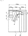
- Fig. 2 shows a plan view of an optical transmitter according to a first embodiment of the present invention.
- the optical transmitter according to the first embodiment of the present invention adopts a subassembly of an optical transmitter module including, on a subcarrier 1 in a width direction of the subcarrier 1, an RF wiring board 20 that integrates a terminating resistor 6, an EA-DFB laser chip 3 having a bent waveguide of approximately 5 degrees, and a capacitor 7 connected to a ground pad 8.
- the terminating resistor 6 with a width that is more or less the same as a width of an RF wiring is integrated at a termination of the RF wiring on the RF wiring board 20 and a width of the subcarrier 1 can be conserved accordingly.
- a wire 11 is drawn out from an end of the RF wiring that is connected to one end of the terminating resistor 6 of the RF wiring board 20 integrating the terminating resistor 6 and connected to an electrode of an EA modulator 5, and supplies a modulated electric signal to the EA modulator 5.
- a wire 12 is drawn out from an electrode connected to another end of the terminating resistor 6 integrated on the RF wiring board 20 and connected to an end of the capacitor 7 for DC interruption (DC cut) across the EA-DFB laser chip 3. Another end of the capacitor 7 is connected to and grounded by the ground pad 8.
- a width of the subcarrier 1 can be reduced by an amount corresponding to lengths of the terminating resistor 6 integrated on the RF wiring board 20 and the electrodes to 0.75 mm.
- an optical transmitter subassembly was created using the same EA-DFB laser chip 3 by applying a conventional structure. This is a structure as shown in Fig. 1 .
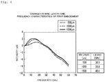
- Figs. 3 and 4 show changes in frequency response characteristics of the respective created optical transmitter subassemblies obtained by changing the wire length in three different ways.
- Fig. 3 represents a case of the conventional example and
- Fig. 4 represents a case of the first embodiment of the present invention.
- Values of frequencies in the 3 dB band that correspond to the three different wire lengths of each wire are also shown in tables provided in lower right parts of Figs. 3 and 4 .
- EA lengths of both wires are set to 130 ⁇ m, a resistance value of the terminating resistor is set to 50 ⁇ , a length of the wire 11 connecting the EA modulator and the RF wiring board to each other is set to 220 ⁇ m, and a capacity of the capacitor is set to 0.1 ⁇ F.
- the frequency response characteristics of the optical transmitter when conventional art is applied are as shown in Fig. 3
- the frequency response characteristics when the first embodiment of the present invention is applied are as shown in Fig. 4 .
- the three graphs of frequency response characteristics represent changes when lengths of the wires 10 and 12 shown in Figs. 1 and 2 are changed in three different ways.
- the 3 dB band at the time of the design value is 39.9 GHz which means that a band almost comparable to conventional art is obtained and, at the same time, even a wire length fluctuation of ⁇ 500 ⁇ m results in only a maximum fluctuation of the 3 dB band of around 1.4 GHz.
- This result indicates that, compared to the conventional structure, the structure according to the first embodiment has extremely large tolerance with respect to a fluctuation in the length of a wire.
- the width in the structure according to the first embodiment is 0.75 mm, which represents a reduction in width by 0.2 mm.
- Fig. 5 is a plan view of an optical transmitter according to a second embodiment of the present invention.
- a subcarrier is created using a component in which the terminating resistor 6 is integrated on the subcarrier 1 unlike in the first embodiment.
- the capacitor 7 for DC interruption is also integrated on the subcarrier 1.
- the capacitor 7 is positioned on a side of the RF wiring board 2 which is an opposite side to the terminating resistor 6 with the EA-DFB laser chip 3 therebetween and provided in an orientation so as to have an end electrode in a width direction of an RF wiring as a separate part to the RF wiring board 2.
- An end electrode on a right side of the capacitor 7 is connected to and grounded by the ground pad 8 positioned in an upper right corner of the subcarrier 1, and an end electrode on a left side of the capacitor 7 is drawn out by a wire 13 and connected to one end of the terminating resistor 6 across the EA-DFB laser chip 3.
- the terminating resistor 6 is arranged in an orientation which causes end electrodes to be positioned above and below unlike in the conventional example, another end of the terminating resistor 6 is connected to the electrode of the EA modulator 5 by the wire 10 in a similar manner to the conventional example, and the electrode of the EA modulator 5 is supplied with a modulated electric signal by the wire 11 from an upper end of the RF wiring.
- Fig. 6 shows fluctuations of frequency response characteristics with respect to a sum of the wire 13 and the wires 10 and 11 (a sum of lengths of wires on an electric path which starts at the RF wiring board, passes through the terminating resistor, and reaches the ground pad) of the created optical transmitter subassembly according to the second embodiment.
- the 3 dB band is 42.4 GHz, thereby enabling a band improvement of around 2 GHz as compared to the 3 dB band according to the conventional structure to be confirmed.
- the 3 dB band even when there is a wire length fluctuation of ⁇ 500 ⁇ m, the 3 dB band only fluctuates by around 0.8 GHz at a maximum. This result indicates that, compared to the conventional structure, the structure according to the second embodiment has extremely large tolerance for fluctuations in the length of a wire.
- the width in the structure according to the second embodiment is 0.75 mm, which represents a reduction in the width by 0.2 mm. This is also attributable to the fact that it is possible to absorb a relatively small width of the terminating resistor 6 by an open area in an upper left corner of the EA-DFB laser chip 3 having been obliquely arranged.
- the capacitor 7 for DC cut need only interrupt DC voltage that is applied to the EA modulator 5 on an electric path which starts at the RF wiring board 2, passes through the terminating resistor 6, and reaches the ground pad 8, at least one capacitor need only be connected in series as a circuit on the electric path.
- the terminating resistor 6 may be the terminating resistor 6 having been monolithically integrated on the subcarrier 1.
- the laser chip is not limited thereto and may be a modulated laser chip having an optical modulation function.
- an optical transmitter capable of significantly suppressing a fluctuation in frequency response characteristics due to a fabrication error in internal wire length while reducing a subcarrier size of a module can be provided.
Landscapes
- Physics & Mathematics (AREA)
- Condensed Matter Physics & Semiconductors (AREA)
- General Physics & Mathematics (AREA)
- Electromagnetism (AREA)
- Optics & Photonics (AREA)
- Semiconductor Lasers (AREA)
- Optical Communication System (AREA)
- Optical Modulation, Optical Deflection, Nonlinear Optics, Optical Demodulation, Optical Logic Elements (AREA)
Abstract
Description
- The present invention relates to an optical transmitter constituted by a semiconductor laser-mounted module.
- Conventionally, an optical transmitter used in optical communications and the like is constituted by an EA-DFB laser-mounted module such as that shown in
Fig. 1 . In the EA-DFB laser-mounted module shown inFig. 1 , anRF wiring board 2, an EA-DFBlaser chip 3 including a DFBlaser 4 and anEA modulator 5, a terminatingresistor 6, and acapacitor 7 are arranged on asubcarrier 1 from the right in the diagram in a width direction (a direction of a short side that is orthogonal to a light-outgoing direction) of thesubcarrier 1. In addition, an upper end of an RF wiring on theRF wiring board 2 and an electrode of theEA modulator 5 on the EA-DFBlaser chip 3 are electrically connected by awire 11, and the electrode of theEA modulator 5 and the terminatingresistor 6 are electrically connected by awire 10. - In the conventional optical transmitter shown in
Fig. 1 , a modulated electric signal input from a lower end of the RF wiring of theRF wiring board 2 is supplied from the upper end of the RF wiring of theRF wiring board 2 to the electrode of theEA modulator 5 via thewire 11 and further connected to an electrode at one end of the terminatingresistor 6 by thewire 10 via the electrode of theEA modulator 5. Another end of the terminatingresistor 6 is connected to one end of thecapacitor 7 for DC interruption (DC cut) via an electrode and connected to and grounded by aground pad 8 to be a ground electrode at another end of thecapacitor 7. As shown inFig. 1 , a conventional optical transmitter requires a width of around 0.95 mm as a size of thesubcarrier 1. - In addition, an optical waveguide of the EA-DFB
laser chip 3 is formed as a bent waveguide as a measure against return light, and a portion of an output optical waveguide is structured to emit light at a non-90 degree angle with respect to a light-outgoing end surface of the EA-DFBlaser chip 3. In order to align a direction of outgoing light in a longitudinal direction of thesubcarrier 1, the EA-DFBlaser chip 3 itself is arranged at an oblique angle in an orientation that enables a side of thesubcarrier 1 in the longitudinal direction and outgoing light to be parallel to each other. - In addition, while the EA-DFB
laser chip 3 including the DFBlaser 4 and theEA modulator 5 has been exemplified as a laser chip, the laser chip is not limited thereto and may be a modulated laser chip of any type with a modulation function. - [NPL 1] C. Kazmierski, A. Konczykowska, F. Jorge, F. Blache, M. Riet, C. Jany, A. Scavennec, "100 Gb/s Operation of an AlGaInAs Semi-Insulating Buried Heterojunction EML", Proc OFC2009 OThT7
- In the conventional optical transmitter shown in
Fig. 1 , since a portion of thewire 10 that connects theEA modulator 5 and the terminatingresistor 6 to each other has parasitic inductance (parastic inductance) in accordance with a length of thewire 10, an effect of adjusting a peaking amount of frequency response characteristics of the optical transmitter is produced. In conventional configurations, there is a problem in that, while a wire length is around 0.2 to 0.3 mm, a fluctuation in peaking in the frequency response characteristics of the optical transmitter that is attributable to fabrication error in the wire length in this case creates a variation in a 3 dB band frequency where gain drops by 3 dB in the frequency response characteristics. - There is another problem in that, when extending the wire length in order to alleviate the variation and arranging the terminating
resistor 6 at a position separated from the EA-DFBlaser chip 3, a size of thesubcarrier 1 increases. - In addition, another problem of the conventional configuration shown in
Fig. 1 is that, since respective parts are generally mounted side by side in a width direction of the subcarrier, a width of the subcarrier increases. - The present invention has been made in consideration of the problems described above and an object thereof is to provide an optical transmitter capable of significantly suppressing a fluctuation in frequency response characteristics due to a fabrication error in internal wire length while reducing a subcarrier size of a module of the optical transmitter.
- In order to achieve the object described above, the present invention characteristically includes the following configurations.
- An optical transmitter, including: a subcarrier on which an RF wiring board, a modulated laser chip, and a terminating resistor are mounted and which has a ground pad on an upper surface thereof; and a wire for electrically connecting at least a part of an electric path which starts at the RF wiring board, passes through the terminating resistor, and reaches the ground pad, wherein the RF wiring board and the modulated laser chip are arranged in a width direction of the subcarrier, and a length of the wire in the electric path which starts at the RF wiring board, passes through the terminating resistor, and reaches the ground pad ranges from 0.5 to 1.5 mm or an inductance of the wire ranges from 0.4 to 1.2 nH.
- The optical transmitter according to
configuration 1, wherein the terminating resistor is monolithically integrated on the RF wiring board or on the subcarrier. - The optical transmitter according to
configuration 1, wherein at least one capacitor is connected in series as a circuit to the electric path which starts at the RF wiring board, passes through the terminating resistor, and reaches the ground pad. - The optical transmitter according to
configuration 3, wherein the capacitor is arranged on an opposite side to the terminating resistor with the modulated laser chip therebetween. - The optical transmitter according to
configuration 1, wherein an output optical waveguide of the modulated laser chip emits light at a non-90 degree angle with respect to a light-outgoing end surface of the modulated laser chip. - As described above, according to the present invention, an optical transmitter capable of significantly suppressing a fluctuation in frequency response characteristics due to a fabrication error in internal wire length while reducing a subcarrier size of a module of the optical transmitter can be provided.
-
- [
Fig. 1 ]
Fig. 1 is a plan view of a module of a conventional optical transmitter. - [
Fig. 2 ]
Fig. 2 is a plan view of a module of an optical transmitter according to a first embodiment of the present invention. - [
Fig. 3 ]
Fig. 3 is a diagram showing a change in frequency response characteristics when changing a wire length in conventional art. - [
Fig. 4 ]
Fig. 4 is a diagram showing a change in frequency response characteristics when changing a wire length in the first embodiment of the present invention. - [
Fig. 5 ]
Fig. 5 is a plan view of a module of an optical transmitter according to a second embodiment of the present invention. - [
Fig. 6 ]
Fig. 6 is a diagram showing a change in frequency response characteristics when changing a wire length in the second embodiment of the present invention. - In order to solve the problems described above, an optical transmitter according to the present invention arranges a terminating resistor, an EA-DFB laser chip, and a ground pad on a subcarrier in a width direction of the subcarrier. Studies conducted based on embodiments described hereinafter revealed that a structure such as that described below is optimal for suppressing a change in frequency response characteristics of an optical transmitter. The structure includes an inductor in which a length of a wire existing on an electric circuit which starts at the RF wiring board, passes through the terminating resistor, and reaches the ground pad ranges from around 0.5 to 1.5 mm or an inductance of the wire corresponds to a total range of 0.4 to 1.2 nH. Adopting such a structure enables a fluctuation of a 3 dB band due to a variation in a length of a wire connecting the ground pad and the terminating resistor to each other to be suppressed and enables a mounting yield to be improved. In addition, a width of the subcarrier can be reduced.
- The present invention achieves stable frequency response characteristics independent of a wire length and a reduction in a width of a subcarrier by optimally designing an arrangement of each part on the subcarrier and a wire length.
- Hereinafter, embodiments of the present invention will be described in detail with reference to the drawings.
-
Fig. 2 shows a plan view of an optical transmitter according to a first embodiment of the present invention. The optical transmitter according to the first embodiment of the present invention adopts a subassembly of an optical transmitter module including, on asubcarrier 1 in a width direction of thesubcarrier 1, anRF wiring board 20 that integrates a terminatingresistor 6, an EA-DFBlaser chip 3 having a bent waveguide of approximately 5 degrees, and acapacitor 7 connected to aground pad 8. - In the optical transmitter according to the first embodiment shown in
Fig. 2 , the terminatingresistor 6 with a width that is more or less the same as a width of an RF wiring is integrated at a termination of the RF wiring on theRF wiring board 20 and a width of thesubcarrier 1 can be conserved accordingly. - A
wire 11 is drawn out from an end of the RF wiring that is connected to one end of the terminatingresistor 6 of theRF wiring board 20 integrating the terminatingresistor 6 and connected to an electrode of anEA modulator 5, and supplies a modulated electric signal to theEA modulator 5. Awire 12 is drawn out from an electrode connected to another end of the terminatingresistor 6 integrated on theRF wiring board 20 and connected to an end of thecapacitor 7 for DC interruption (DC cut) across the EA-DFBlaser chip 3. Another end of thecapacitor 7 is connected to and grounded by theground pad 8. As shown inFig. 2 , in the optical transmitter according to the first embodiment, a width of thesubcarrier 1 can be reduced by an amount corresponding to lengths of the terminatingresistor 6 integrated on theRF wiring board 20 and the electrodes to 0.75 mm. - For comparison, an optical transmitter subassembly was created using the same EA-DFB
laser chip 3 by applying a conventional structure. This is a structure as shown inFig. 1 . -
Figs. 3 and4 show changes in frequency response characteristics of the respective created optical transmitter subassemblies obtained by changing the wire length in three different ways.Fig. 3 represents a case of the conventional example andFig. 4 represents a case of the first embodiment of the present invention. Values of frequencies in the 3 dB band that correspond to the three different wire lengths of each wire (inFig. 3 , thewire 10 shown inFig. 1 , and inFig. 4 , thewire 12 shown inFig. 2 ) are also shown in tables provided in lower right parts ofFigs. 3 and4 . EA lengths of both wires are set to 130 µm, a resistance value of the terminating resistor is set to 50 Ω, a length of thewire 11 connecting the EA modulator and the RF wiring board to each other is set to 220 µm, and a capacity of the capacitor is set to 0.1 µF. - The frequency response characteristics of the optical transmitter when conventional art is applied are as shown in
Fig. 3 , and the frequency response characteristics when the first embodiment of the present invention is applied are as shown inFig. 4 . The three graphs of frequency response characteristics represent changes when lengths of thewires Figs. 1 and2 are changed in three different ways. - When conventional art is applied (
Figs. 1 and3 ), with respect to adesign value 300 µm of thewire 10, the 3 dB band at the time of the design value is 40.1 GHz, and a wire length fluctuation of ±100 µm results in a maximum fluctuation of the 3 dB band of around 3.3 GHz. In contrast, when the first embodiment of the present invention is applied (Figs. 2 and4 ), with respect to adesign value 1000 µm of thewire 12, the 3 dB band at the time of the design value is 39.9 GHz which means that a band almost comparable to conventional art is obtained and, at the same time, even a wire length fluctuation of ±500 µm results in only a maximum fluctuation of the 3 dB band of around 1.4 GHz. This result indicates that, compared to the conventional structure, the structure according to the first embodiment has extremely large tolerance with respect to a fluctuation in the length of a wire. - In addition, it is confirmed that, even when comparing widths of the created subassemblies, with respect to 0.95 mm for the conventional type, the width in the structure according to the first embodiment is 0.75 mm, which represents a reduction in width by 0.2 mm.
-
Fig. 5 is a plan view of an optical transmitter according to a second embodiment of the present invention. In the optical transmitter according to the second embodiment of the present invention, using the same EA-DFB laser chip 3 as the first embodiment, a subcarrier is created using a component in which the terminatingresistor 6 is integrated on thesubcarrier 1 unlike in the first embodiment. - In the optical transmitter subassembly according to the second embodiment shown in
Fig. 5 , thecapacitor 7 for DC interruption (DC cut) is also integrated on thesubcarrier 1. However, unlike both the first embodiment and the conventional example, thecapacitor 7 is positioned on a side of theRF wiring board 2 which is an opposite side to the terminatingresistor 6 with the EA-DFB laser chip 3 therebetween and provided in an orientation so as to have an end electrode in a width direction of an RF wiring as a separate part to theRF wiring board 2. - An end electrode on a right side of the
capacitor 7 is connected to and grounded by theground pad 8 positioned in an upper right corner of thesubcarrier 1, and an end electrode on a left side of thecapacitor 7 is drawn out by awire 13 and connected to one end of the terminatingresistor 6 across the EA-DFB laser chip 3. - The terminating
resistor 6 is arranged in an orientation which causes end electrodes to be positioned above and below unlike in the conventional example, another end of the terminatingresistor 6 is connected to the electrode of theEA modulator 5 by thewire 10 in a similar manner to the conventional example, and the electrode of theEA modulator 5 is supplied with a modulated electric signal by thewire 11 from an upper end of the RF wiring. -
Fig. 6 shows fluctuations of frequency response characteristics with respect to a sum of thewire 13 and thewires 10 and 11 (a sum of lengths of wires on an electric path which starts at the RF wiring board, passes through the terminating resistor, and reaches the ground pad) of the created optical transmitter subassembly according to the second embodiment. When the sum of the lengths of the wires is a design value, the 3 dB band is 42.4 GHz, thereby enabling a band improvement of around 2 GHz as compared to the 3 dB band according to the conventional structure to be confirmed. In addition, even when there is a wire length fluctuation of ±500 µm, the 3 dB band only fluctuates by around 0.8 GHz at a maximum. This result indicates that, compared to the conventional structure, the structure according to the second embodiment has extremely large tolerance for fluctuations in the length of a wire. - In addition, it is confirmed that, even when comparing widths of the created subassemblies, with respect to 0.95 mm for the conventional type, the width in the structure according to the second embodiment is 0.75 mm, which represents a reduction in the width by 0.2 mm. This is also attributable to the fact that it is possible to absorb a relatively small width of the terminating
resistor 6 by an open area in an upper left corner of the EA-DFB laser chip 3 having been obliquely arranged. - Moreover, since the
capacitor 7 for DC cut need only interrupt DC voltage that is applied to theEA modulator 5 on an electric path which starts at theRF wiring board 2, passes through the terminatingresistor 6, and reaches theground pad 8, at least one capacitor need only be connected in series as a circuit on the electric path. In addition, the terminatingresistor 6 may be the terminatingresistor 6 having been monolithically integrated on thesubcarrier 1. - While both embodiments adopt the EA-
DFB laser chip 3 as a laser chip in the present invention, it is obvious that the laser chip is not limited thereto and may be a modulated laser chip having an optical modulation function. - As described above, with the optical transmitter according to the present invention, an optical transmitter capable of significantly suppressing a fluctuation in frequency response characteristics due to a fabrication error in internal wire length while reducing a subcarrier size of a module can be provided.
-
- 1
- Subcarrier
- 2, 20
- RF wiring board
- 3
- EA-DFB laser chip
- 4
- DFB laser
- 5
- EA modulator
- 6
- Terminating resistor
- 7
- Capacitor
- 8
- Ground pad
- 10, 11, 12, 13
- Wire
Claims (5)
- An optical transmitter, comprising: a subcarrier on which an RF wiring board, a modulated laser chip, and a terminating resistor are mounted and which has a ground pad on an upper surface thereof; and a wire for electrically connecting at least a part of an electric path which starts at the RF wiring board, passes through the terminating resistor, and reaches the ground pad, wherein the RF wiring board and the modulated laser chip are arranged in a width direction of the subcarrier, and a length of the wire in the electric path which starts at the RF wiring board, passes through the terminating resistor, and reaches the ground pad ranges from 0.5 to 1.5 mm or an inductance of the wire ranges from 0.4 to 1.2 nH.
- The optical transmitter according to claim 1, wherein the terminating resistor is monolithically integrated on the RF wiring board or on the subcarrier.
- The optical transmitter according to claim 1, wherein at least one capacitor is connected in series as a circuit to the electric path which starts at the RF wiring board, passes through the terminating resistor, and reaches the ground pad.
- The optical transmitter according to claim 3, wherein the capacitor is arranged on an opposite side to the terminating resistor with the modulated laser chip therebetween.
- The optical transmitter according to claim 1, wherein an output optical waveguide of the modulated laser chip emits light at a non-90 degree angle with respect to a light-outgoing end surface of the modulated laser chip.
Applications Claiming Priority (2)
| Application Number | Priority Date | Filing Date | Title |
|---|---|---|---|
| JP2019019720A JP7124741B2 (en) | 2019-02-06 | 2019-02-06 | optical transmitter |
| PCT/JP2020/002453 WO2020162217A1 (en) | 2019-02-06 | 2020-01-24 | Optical transmitter |
Publications (3)
| Publication Number | Publication Date |
|---|---|
| EP3923425A1 true EP3923425A1 (en) | 2021-12-15 |
| EP3923425A4 EP3923425A4 (en) | 2022-11-02 |
| EP3923425B1 EP3923425B1 (en) | 2024-03-20 |
Family
ID=71947295
Family Applications (1)
| Application Number | Title | Priority Date | Filing Date |
|---|---|---|---|
| EP20752773.0A Active EP3923425B1 (en) | 2019-02-06 | 2020-01-24 | Optical transmitter |
Country Status (5)
| Country | Link |
|---|---|
| US (1) | US12444902B2 (en) |
| EP (1) | EP3923425B1 (en) |
| JP (1) | JP7124741B2 (en) |
| CN (1) | CN113366715B (en) |
| WO (1) | WO2020162217A1 (en) |
Cited By (1)
| Publication number | Priority date | Publication date | Assignee | Title |
|---|---|---|---|---|
| EP4481962A4 (en) * | 2022-02-14 | 2026-03-04 | Ntt Inc | OPTICAL TRANSMITTER |
Families Citing this family (4)
| Publication number | Priority date | Publication date | Assignee | Title |
|---|---|---|---|---|
| JP7437278B2 (en) * | 2020-09-25 | 2024-02-22 | CIG Photonics Japan株式会社 | optical module |
| JP7502983B2 (en) | 2020-12-23 | 2024-06-19 | CIG Photonics Japan株式会社 | Optical Modules |
| CN115912045A (en) * | 2021-08-20 | 2023-04-04 | 苏州旭创科技有限公司 | Electric absorption modulation laser chip and laser chip packaging structure |
| US20250038857A1 (en) * | 2021-12-07 | 2025-01-30 | Nippon Telegraph And Telephone Corporation | Optical Circuit |
Family Cites Families (23)
| Publication number | Priority date | Publication date | Assignee | Title |
|---|---|---|---|---|
| JP3553222B2 (en) * | 1995-09-20 | 2004-08-11 | 三菱電機株式会社 | Optical modulator module |
| JPH1051069A (en) | 1996-07-29 | 1998-02-20 | Mitsubishi Electric Corp | Optical semiconductor device |
| DE59901985D1 (en) * | 1998-05-26 | 2002-08-14 | Infineon Technologies Ag | High-frequency laser module and method for producing the same |
| JP2001209017A (en) * | 1999-11-15 | 2001-08-03 | Mitsubishi Electric Corp | Photoelectric conversion semiconductor device |
| JP4290314B2 (en) | 2000-04-26 | 2009-07-01 | Necエレクトロニクス株式会社 | High-frequency circuit, module mounted with the same, and communication device |
| JP2002111110A (en) | 2000-09-27 | 2002-04-12 | Toshiba Corp | Optical communication module |
| JP2002368325A (en) | 2001-06-11 | 2002-12-20 | Hitachi Ltd | Light emitting module, optical semiconductor element, and light receiving module |
| US6873449B1 (en) * | 2003-09-05 | 2005-03-29 | The Furukawa Electric Co., Ltd. | Signal transmission line for an optical modulator |
| JP4393187B2 (en) | 2003-12-26 | 2010-01-06 | 日本オプネクスト株式会社 | Chip carrier for semiconductor optical device, optical module, and optical transceiver |
| JP2005338678A (en) * | 2004-05-31 | 2005-12-08 | Opnext Japan Inc | Optical modulator module |
| US7011458B2 (en) * | 2004-07-12 | 2006-03-14 | Opnext Japan, Inc. | Optical module |
| JP4578164B2 (en) | 2004-07-12 | 2010-11-10 | 日本オプネクスト株式会社 | Optical module |
| JP4856465B2 (en) * | 2006-04-19 | 2012-01-18 | 日本オプネクスト株式会社 | Optical semiconductor element mounting substrate and optical transmission module |
| US7539228B2 (en) | 2007-06-26 | 2009-05-26 | Avago Technologies Fiber Ip (Singapore) Pte. Ltd. | Integrated photonic semiconductor devices having ridge structures that are grown rather than etched, and methods for making same |
| JP5483677B2 (en) * | 2009-04-02 | 2014-05-07 | ネオフォトニクス・セミコンダクタ合同会社 | Semiconductor optical communication module and manufacturing method thereof |
| JP5475404B2 (en) | 2009-11-12 | 2014-04-16 | 日本オクラロ株式会社 | Chip carrier and optical communication module |
| JP2013015670A (en) * | 2011-07-04 | 2013-01-24 | Sumitomo Electric Device Innovations Inc | Optical modulation device |
| CN105264430B (en) * | 2013-12-05 | 2019-05-28 | 华为技术有限公司 | An optical modulator and a planar photonic device module |
| CN107430293B (en) * | 2015-03-23 | 2021-02-26 | 日本电信电话株式会社 | Optical circuit |
| JP6502844B2 (en) | 2015-12-28 | 2019-04-17 | 日本電信電話株式会社 | Optical semiconductor device |
| WO2017135381A1 (en) * | 2016-02-04 | 2017-08-10 | 日本電信電話株式会社 | Optical transmitter and light intensity monitoring method |
| CN108780235B (en) * | 2016-03-18 | 2021-12-14 | 日本电信电话株式会社 | light modulator |
| JP6926562B2 (en) | 2017-03-21 | 2021-08-25 | 住友電気工業株式会社 | Light modulator module |
-
2019
- 2019-02-06 JP JP2019019720A patent/JP7124741B2/en active Active
-
2020
- 2020-01-24 WO PCT/JP2020/002453 patent/WO2020162217A1/en not_active Ceased
- 2020-01-24 CN CN202080011532.9A patent/CN113366715B/en active Active
- 2020-01-24 US US17/428,059 patent/US12444902B2/en active Active
- 2020-01-24 EP EP20752773.0A patent/EP3923425B1/en active Active
Cited By (1)
| Publication number | Priority date | Publication date | Assignee | Title |
|---|---|---|---|---|
| EP4481962A4 (en) * | 2022-02-14 | 2026-03-04 | Ntt Inc | OPTICAL TRANSMITTER |
Also Published As
| Publication number | Publication date |
|---|---|
| JP2020127168A (en) | 2020-08-20 |
| EP3923425B1 (en) | 2024-03-20 |
| EP3923425A4 (en) | 2022-11-02 |
| US12444902B2 (en) | 2025-10-14 |
| CN113366715A (en) | 2021-09-07 |
| JP7124741B2 (en) | 2022-08-24 |
| CN113366715B (en) | 2024-01-09 |
| US20220149591A1 (en) | 2022-05-12 |
| WO2020162217A1 (en) | 2020-08-13 |
Similar Documents
| Publication | Publication Date | Title |
|---|---|---|
| EP3923425B1 (en) | Optical transmitter | |
| US7400791B2 (en) | Semiconductor element mounting board and optical transmission module | |
| US6437899B1 (en) | Opto-electric conversion semiconductor device | |
| CN107430293B (en) | Optical circuit | |
| KR101512816B1 (en) | Flexible printed circuit board and optical communication module comprising the same | |
| JP5881752B2 (en) | Transistor outline housing and manufacturing method thereof | |
| US8987650B2 (en) | Front end module for optical receiver | |
| EP1605295B1 (en) | Optical modulator module | |
| JP6228561B2 (en) | High frequency transmission line and optical circuit | |
| US20210057877A1 (en) | Optical semiconductor device and carrier | |
| US12094840B2 (en) | Semiconductor device capable of realizing a wide band impedance matching | |
| US20160066425A1 (en) | Flexible printed circuit (fpc) board | |
| EP1826927B1 (en) | Optical receiver module | |
| CN217639660U (en) | Optical module and light emitting device | |
| JP6228560B2 (en) | High frequency transmission line and optical circuit | |
| US12562548B2 (en) | Optical semiconductor device | |
| US7196909B2 (en) | AC coupling circuit having a large capacitance and a good frequency response | |
| US6788447B2 (en) | Off-chip matching circuit for electroabsorption optical modulator | |
| US11469192B2 (en) | Semiconductor device capable of realizing a wide band impedance matching | |
| US11909170B2 (en) | Semiconductor light emitting device and optical subassembly | |
| US20010021054A1 (en) | Optical telecommunication module | |
| JP2007266493A (en) | Laser module | |
| JP7654134B1 (en) | Modulation Circuit | |
| US5525841A (en) | Power gaAs fet having internal matching circuit | |
| CN105164856B (en) | Substrate for antenna device and antenna device |
Legal Events
| Date | Code | Title | Description |
|---|---|---|---|
| STAA | Information on the status of an ep patent application or granted ep patent |
Free format text: STATUS: THE INTERNATIONAL PUBLICATION HAS BEEN MADE |
|
| PUAI | Public reference made under article 153(3) epc to a published international application that has entered the european phase |
Free format text: ORIGINAL CODE: 0009012 |
|
| STAA | Information on the status of an ep patent application or granted ep patent |
Free format text: STATUS: REQUEST FOR EXAMINATION WAS MADE |
|
| 17P | Request for examination filed |
Effective date: 20210804 |
|
| AK | Designated contracting states |
Kind code of ref document: A1 Designated state(s): AL AT BE BG CH CY CZ DE DK EE ES FI FR GB GR HR HU IE IS IT LI LT LU LV MC MK MT NL NO PL PT RO RS SE SI SK SM TR |
|
| DAV | Request for validation of the european patent (deleted) | ||
| DAX | Request for extension of the european patent (deleted) | ||
| REG | Reference to a national code |
Ref country code: DE Ref legal event code: R079 Free format text: PREVIOUS MAIN CLASS: H01S0005022000 Ipc: H01S0005023450 Ref document number: 602020027554 Country of ref document: DE |
|
| A4 | Supplementary search report drawn up and despatched |
Effective date: 20221006 |
|
| RIC1 | Information provided on ipc code assigned before grant |
Ipc: H01S 5/12 20210101ALN20220929BHEP Ipc: H01S 5/10 20210101ALN20220929BHEP Ipc: H01S 5/062 20060101ALN20220929BHEP Ipc: H01S 5/026 20060101ALN20220929BHEP Ipc: H01S 5/0239 20210101ALI20220929BHEP Ipc: H01S 5/02345 20210101AFI20220929BHEP |
|
| STAA | Information on the status of an ep patent application or granted ep patent |
Free format text: STATUS: EXAMINATION IS IN PROGRESS |
|
| 17Q | First examination report despatched |
Effective date: 20230525 |
|
| GRAP | Despatch of communication of intention to grant a patent |
Free format text: ORIGINAL CODE: EPIDOSNIGR1 |
|
| STAA | Information on the status of an ep patent application or granted ep patent |
Free format text: STATUS: GRANT OF PATENT IS INTENDED |
|
| RIC1 | Information provided on ipc code assigned before grant |
Ipc: H01L 23/00 20060101ALN20231006BHEP Ipc: H01S 5/12 20210101ALN20231006BHEP Ipc: H01S 5/10 20210101ALN20231006BHEP Ipc: H01S 5/062 20060101ALN20231006BHEP Ipc: H01S 5/026 20060101ALN20231006BHEP Ipc: H01S 5/0239 20210101ALI20231006BHEP Ipc: H01S 5/02345 20210101AFI20231006BHEP |
|
| INTG | Intention to grant announced |
Effective date: 20231025 |
|
| RIN1 | Information on inventor provided before grant (corrected) |
Inventor name: FUJIWARA, NAOKI Inventor name: SHINDO, TAKAHIKO Inventor name: KANAZAWA, SHIGERU |
|
| GRAS | Grant fee paid |
Free format text: ORIGINAL CODE: EPIDOSNIGR3 |
|
| GRAA | (expected) grant |
Free format text: ORIGINAL CODE: 0009210 |
|
| STAA | Information on the status of an ep patent application or granted ep patent |
Free format text: STATUS: THE PATENT HAS BEEN GRANTED |
|
| AK | Designated contracting states |
Kind code of ref document: B1 Designated state(s): AL AT BE BG CH CY CZ DE DK EE ES FI FR GB GR HR HU IE IS IT LI LT LU LV MC MK MT NL NO PL PT RO RS SE SI SK SM TR |
|
| REG | Reference to a national code |
Ref country code: GB Ref legal event code: FG4D |
|
| REG | Reference to a national code |
Ref country code: CH Ref legal event code: EP |
|
| REG | Reference to a national code |
Ref country code: IE Ref legal event code: FG4D |
|
| REG | Reference to a national code |
Ref country code: DE Ref legal event code: R096 Ref document number: 602020027554 Country of ref document: DE |
|
| PG25 | Lapsed in a contracting state [announced via postgrant information from national office to epo] |
Ref country code: LT Free format text: LAPSE BECAUSE OF FAILURE TO SUBMIT A TRANSLATION OF THE DESCRIPTION OR TO PAY THE FEE WITHIN THE PRESCRIBED TIME-LIMIT Effective date: 20240320 |
|
| REG | Reference to a national code |
Ref country code: LT Ref legal event code: MG9D |
|
| PG25 | Lapsed in a contracting state [announced via postgrant information from national office to epo] |
Ref country code: GR Free format text: LAPSE BECAUSE OF FAILURE TO SUBMIT A TRANSLATION OF THE DESCRIPTION OR TO PAY THE FEE WITHIN THE PRESCRIBED TIME-LIMIT Effective date: 20240621 |
|
| PG25 | Lapsed in a contracting state [announced via postgrant information from national office to epo] |
Ref country code: RS Free format text: LAPSE BECAUSE OF FAILURE TO SUBMIT A TRANSLATION OF THE DESCRIPTION OR TO PAY THE FEE WITHIN THE PRESCRIBED TIME-LIMIT Effective date: 20240620 Ref country code: HR Free format text: LAPSE BECAUSE OF FAILURE TO SUBMIT A TRANSLATION OF THE DESCRIPTION OR TO PAY THE FEE WITHIN THE PRESCRIBED TIME-LIMIT Effective date: 20240320 |
|
| REG | Reference to a national code |
Ref country code: NL Ref legal event code: MP Effective date: 20240320 |
|
| PG25 | Lapsed in a contracting state [announced via postgrant information from national office to epo] |
Ref country code: RS Free format text: LAPSE BECAUSE OF FAILURE TO SUBMIT A TRANSLATION OF THE DESCRIPTION OR TO PAY THE FEE WITHIN THE PRESCRIBED TIME-LIMIT Effective date: 20240620 Ref country code: NO Free format text: LAPSE BECAUSE OF FAILURE TO SUBMIT A TRANSLATION OF THE DESCRIPTION OR TO PAY THE FEE WITHIN THE PRESCRIBED TIME-LIMIT Effective date: 20240620 Ref country code: LT Free format text: LAPSE BECAUSE OF FAILURE TO SUBMIT A TRANSLATION OF THE DESCRIPTION OR TO PAY THE FEE WITHIN THE PRESCRIBED TIME-LIMIT Effective date: 20240320 Ref country code: HR Free format text: LAPSE BECAUSE OF FAILURE TO SUBMIT A TRANSLATION OF THE DESCRIPTION OR TO PAY THE FEE WITHIN THE PRESCRIBED TIME-LIMIT Effective date: 20240320 Ref country code: GR Free format text: LAPSE BECAUSE OF FAILURE TO SUBMIT A TRANSLATION OF THE DESCRIPTION OR TO PAY THE FEE WITHIN THE PRESCRIBED TIME-LIMIT Effective date: 20240621 Ref country code: FI Free format text: LAPSE BECAUSE OF FAILURE TO SUBMIT A TRANSLATION OF THE DESCRIPTION OR TO PAY THE FEE WITHIN THE PRESCRIBED TIME-LIMIT Effective date: 20240320 Ref country code: BG Free format text: LAPSE BECAUSE OF FAILURE TO SUBMIT A TRANSLATION OF THE DESCRIPTION OR TO PAY THE FEE WITHIN THE PRESCRIBED TIME-LIMIT Effective date: 20240320 |
|
| REG | Reference to a national code |
Ref country code: AT Ref legal event code: MK05 Ref document number: 1668680 Country of ref document: AT Kind code of ref document: T Effective date: 20240320 |
|
| PG25 | Lapsed in a contracting state [announced via postgrant information from national office to epo] |
Ref country code: SE Free format text: LAPSE BECAUSE OF FAILURE TO SUBMIT A TRANSLATION OF THE DESCRIPTION OR TO PAY THE FEE WITHIN THE PRESCRIBED TIME-LIMIT Effective date: 20240320 Ref country code: LV Free format text: LAPSE BECAUSE OF FAILURE TO SUBMIT A TRANSLATION OF THE DESCRIPTION OR TO PAY THE FEE WITHIN THE PRESCRIBED TIME-LIMIT Effective date: 20240320 |
|
| PG25 | Lapsed in a contracting state [announced via postgrant information from national office to epo] |
Ref country code: NL Free format text: LAPSE BECAUSE OF FAILURE TO SUBMIT A TRANSLATION OF THE DESCRIPTION OR TO PAY THE FEE WITHIN THE PRESCRIBED TIME-LIMIT Effective date: 20240320 |
|
| PG25 | Lapsed in a contracting state [announced via postgrant information from national office to epo] |
Ref country code: NL Free format text: LAPSE BECAUSE OF FAILURE TO SUBMIT A TRANSLATION OF THE DESCRIPTION OR TO PAY THE FEE WITHIN THE PRESCRIBED TIME-LIMIT Effective date: 20240320 |
|
| PG25 | Lapsed in a contracting state [announced via postgrant information from national office to epo] |
Ref country code: IS Free format text: LAPSE BECAUSE OF FAILURE TO SUBMIT A TRANSLATION OF THE DESCRIPTION OR TO PAY THE FEE WITHIN THE PRESCRIBED TIME-LIMIT Effective date: 20240720 |
|
| PG25 | Lapsed in a contracting state [announced via postgrant information from national office to epo] |
Ref country code: PT Free format text: LAPSE BECAUSE OF FAILURE TO SUBMIT A TRANSLATION OF THE DESCRIPTION OR TO PAY THE FEE WITHIN THE PRESCRIBED TIME-LIMIT Effective date: 20240722 Ref country code: SM Free format text: LAPSE BECAUSE OF FAILURE TO SUBMIT A TRANSLATION OF THE DESCRIPTION OR TO PAY THE FEE WITHIN THE PRESCRIBED TIME-LIMIT Effective date: 20240320 |
|
| PG25 | Lapsed in a contracting state [announced via postgrant information from national office to epo] |
Ref country code: ES Free format text: LAPSE BECAUSE OF FAILURE TO SUBMIT A TRANSLATION OF THE DESCRIPTION OR TO PAY THE FEE WITHIN THE PRESCRIBED TIME-LIMIT Effective date: 20240320 |
|
| PG25 | Lapsed in a contracting state [announced via postgrant information from national office to epo] |
Ref country code: EE Free format text: LAPSE BECAUSE OF FAILURE TO SUBMIT A TRANSLATION OF THE DESCRIPTION OR TO PAY THE FEE WITHIN THE PRESCRIBED TIME-LIMIT Effective date: 20240320 Ref country code: CZ Free format text: LAPSE BECAUSE OF FAILURE TO SUBMIT A TRANSLATION OF THE DESCRIPTION OR TO PAY THE FEE WITHIN THE PRESCRIBED TIME-LIMIT Effective date: 20240320 |
|
| PG25 | Lapsed in a contracting state [announced via postgrant information from national office to epo] |
Ref country code: AT Free format text: LAPSE BECAUSE OF FAILURE TO SUBMIT A TRANSLATION OF THE DESCRIPTION OR TO PAY THE FEE WITHIN THE PRESCRIBED TIME-LIMIT Effective date: 20240320 |
|
| PG25 | Lapsed in a contracting state [announced via postgrant information from national office to epo] |
Ref country code: PL Free format text: LAPSE BECAUSE OF FAILURE TO SUBMIT A TRANSLATION OF THE DESCRIPTION OR TO PAY THE FEE WITHIN THE PRESCRIBED TIME-LIMIT Effective date: 20240320 |
|
| PG25 | Lapsed in a contracting state [announced via postgrant information from national office to epo] |
Ref country code: SK Free format text: LAPSE BECAUSE OF FAILURE TO SUBMIT A TRANSLATION OF THE DESCRIPTION OR TO PAY THE FEE WITHIN THE PRESCRIBED TIME-LIMIT Effective date: 20240320 |
|
| PG25 | Lapsed in a contracting state [announced via postgrant information from national office to epo] |
Ref country code: SM Free format text: LAPSE BECAUSE OF FAILURE TO SUBMIT A TRANSLATION OF THE DESCRIPTION OR TO PAY THE FEE WITHIN THE PRESCRIBED TIME-LIMIT Effective date: 20240320 Ref country code: SK Free format text: LAPSE BECAUSE OF FAILURE TO SUBMIT A TRANSLATION OF THE DESCRIPTION OR TO PAY THE FEE WITHIN THE PRESCRIBED TIME-LIMIT Effective date: 20240320 Ref country code: RO Free format text: LAPSE BECAUSE OF FAILURE TO SUBMIT A TRANSLATION OF THE DESCRIPTION OR TO PAY THE FEE WITHIN THE PRESCRIBED TIME-LIMIT Effective date: 20240320 Ref country code: PT Free format text: LAPSE BECAUSE OF FAILURE TO SUBMIT A TRANSLATION OF THE DESCRIPTION OR TO PAY THE FEE WITHIN THE PRESCRIBED TIME-LIMIT Effective date: 20240722 Ref country code: PL Free format text: LAPSE BECAUSE OF FAILURE TO SUBMIT A TRANSLATION OF THE DESCRIPTION OR TO PAY THE FEE WITHIN THE PRESCRIBED TIME-LIMIT Effective date: 20240320 Ref country code: IS Free format text: LAPSE BECAUSE OF FAILURE TO SUBMIT A TRANSLATION OF THE DESCRIPTION OR TO PAY THE FEE WITHIN THE PRESCRIBED TIME-LIMIT Effective date: 20240720 Ref country code: ES Free format text: LAPSE BECAUSE OF FAILURE TO SUBMIT A TRANSLATION OF THE DESCRIPTION OR TO PAY THE FEE WITHIN THE PRESCRIBED TIME-LIMIT Effective date: 20240320 Ref country code: EE Free format text: LAPSE BECAUSE OF FAILURE TO SUBMIT A TRANSLATION OF THE DESCRIPTION OR TO PAY THE FEE WITHIN THE PRESCRIBED TIME-LIMIT Effective date: 20240320 Ref country code: CZ Free format text: LAPSE BECAUSE OF FAILURE TO SUBMIT A TRANSLATION OF THE DESCRIPTION OR TO PAY THE FEE WITHIN THE PRESCRIBED TIME-LIMIT Effective date: 20240320 Ref country code: AT Free format text: LAPSE BECAUSE OF FAILURE TO SUBMIT A TRANSLATION OF THE DESCRIPTION OR TO PAY THE FEE WITHIN THE PRESCRIBED TIME-LIMIT Effective date: 20240320 |
|
| PG25 | Lapsed in a contracting state [announced via postgrant information from national office to epo] |
Ref country code: IT Free format text: LAPSE BECAUSE OF FAILURE TO SUBMIT A TRANSLATION OF THE DESCRIPTION OR TO PAY THE FEE WITHIN THE PRESCRIBED TIME-LIMIT Effective date: 20240320 |
|
| REG | Reference to a national code |
Ref country code: DE Ref legal event code: R097 Ref document number: 602020027554 Country of ref document: DE |
|
| PG25 | Lapsed in a contracting state [announced via postgrant information from national office to epo] |
Ref country code: IT Free format text: LAPSE BECAUSE OF FAILURE TO SUBMIT A TRANSLATION OF THE DESCRIPTION OR TO PAY THE FEE WITHIN THE PRESCRIBED TIME-LIMIT Effective date: 20240320 |
|
| PG25 | Lapsed in a contracting state [announced via postgrant information from national office to epo] |
Ref country code: DK Free format text: LAPSE BECAUSE OF FAILURE TO SUBMIT A TRANSLATION OF THE DESCRIPTION OR TO PAY THE FEE WITHIN THE PRESCRIBED TIME-LIMIT Effective date: 20240320 |
|
| PLBE | No opposition filed within time limit |
Free format text: ORIGINAL CODE: 0009261 |
|
| STAA | Information on the status of an ep patent application or granted ep patent |
Free format text: STATUS: NO OPPOSITION FILED WITHIN TIME LIMIT |
|
| PG25 | Lapsed in a contracting state [announced via postgrant information from national office to epo] |
Ref country code: DK Free format text: LAPSE BECAUSE OF FAILURE TO SUBMIT A TRANSLATION OF THE DESCRIPTION OR TO PAY THE FEE WITHIN THE PRESCRIBED TIME-LIMIT Effective date: 20240320 |
|
| 26N | No opposition filed |
Effective date: 20241223 |
|
| PG25 | Lapsed in a contracting state [announced via postgrant information from national office to epo] |
Ref country code: SI Free format text: LAPSE BECAUSE OF FAILURE TO SUBMIT A TRANSLATION OF THE DESCRIPTION OR TO PAY THE FEE WITHIN THE PRESCRIBED TIME-LIMIT Effective date: 20240320 |
|
| REG | Reference to a national code |
Ref country code: CH Ref legal event code: PL |
|
| PG25 | Lapsed in a contracting state [announced via postgrant information from national office to epo] |
Ref country code: MC Free format text: LAPSE BECAUSE OF FAILURE TO SUBMIT A TRANSLATION OF THE DESCRIPTION OR TO PAY THE FEE WITHIN THE PRESCRIBED TIME-LIMIT Effective date: 20240320 Ref country code: LU Free format text: LAPSE BECAUSE OF NON-PAYMENT OF DUE FEES Effective date: 20250124 |
|
| PG25 | Lapsed in a contracting state [announced via postgrant information from national office to epo] |
Ref country code: BE Free format text: LAPSE BECAUSE OF NON-PAYMENT OF DUE FEES Effective date: 20250131 |
|
| PG25 | Lapsed in a contracting state [announced via postgrant information from national office to epo] |
Ref country code: CH Free format text: LAPSE BECAUSE OF NON-PAYMENT OF DUE FEES Effective date: 20250131 |
|
| REG | Reference to a national code |
Ref country code: BE Ref legal event code: MM Effective date: 20250131 |
|
| PG25 | Lapsed in a contracting state [announced via postgrant information from national office to epo] |
Ref country code: IE Free format text: LAPSE BECAUSE OF NON-PAYMENT OF DUE FEES Effective date: 20250124 |
|
| REG | Reference to a national code |
Ref country code: DE Ref legal event code: R081 Ref document number: 602020027554 Country of ref document: DE Owner name: NTT, INC., JP Free format text: FORMER OWNER: NIPPON TELEGRAPH AND TELEPHONE CORPORATION, TOKYO, JP Ref country code: DE Ref legal event code: R082 Ref document number: 602020027554 Country of ref document: DE Representative=s name: DENNEMEYER & ASSOCIATES RECHTSANWALTSGESELLSCH, DE |
|
| PGFP | Annual fee paid to national office [announced via postgrant information from national office to epo] |
Ref country code: GB Payment date: 20260123 Year of fee payment: 7 |
|
| PGFP | Annual fee paid to national office [announced via postgrant information from national office to epo] |
Ref country code: DE Payment date: 20260121 Year of fee payment: 7 |
|
| PGFP | Annual fee paid to national office [announced via postgrant information from national office to epo] |
Ref country code: FR Payment date: 20260123 Year of fee payment: 7 |