EP3923358B1 - Method for manufacturing conductive polymer electrode by using drop casting - Google Patents
Method for manufacturing conductive polymer electrode by using drop casting Download PDFInfo
- Publication number
- EP3923358B1 EP3923358B1 EP19922839.6A EP19922839A EP3923358B1 EP 3923358 B1 EP3923358 B1 EP 3923358B1 EP 19922839 A EP19922839 A EP 19922839A EP 3923358 B1 EP3923358 B1 EP 3923358B1
- Authority
- EP
- European Patent Office
- Prior art keywords
- solution
- polymer
- mixing
- mixing solution
- conductive material
- Prior art date
- Legal status (The legal status is an assumption and is not a legal conclusion. Google has not performed a legal analysis and makes no representation as to the accuracy of the status listed.)
- Active
Links
Images



Classifications
-
- H—ELECTRICITY
- H10—SEMICONDUCTOR DEVICES; ELECTRIC SOLID-STATE DEVICES NOT OTHERWISE PROVIDED FOR
- H10K—ORGANIC ELECTRIC SOLID-STATE DEVICES
- H10K71/00—Manufacture or treatment specially adapted for the organic devices covered by this subclass
- H10K71/60—Forming conductive regions or layers, e.g. electrodes
- H10K71/611—Forming conductive regions or layers, e.g. electrodes using printing deposition, e.g. ink jet printing
-
- A—HUMAN NECESSITIES
- A61—MEDICAL OR VETERINARY SCIENCE; HYGIENE
- A61B—DIAGNOSIS; SURGERY; IDENTIFICATION
- A61B5/00—Measuring for diagnostic purposes; Identification of persons
- A61B5/24—Detecting, measuring or recording bioelectric or biomagnetic signals of the body or parts thereof
- A61B5/25—Bioelectric electrodes therefor
- A61B5/263—Bioelectric electrodes therefor characterised by the electrode materials
- A61B5/268—Bioelectric electrodes therefor characterised by the electrode materials containing conductive polymers, e.g. PEDOT:PSS polymers
-
- C—CHEMISTRY; METALLURGY
- C09—DYES; PAINTS; POLISHES; NATURAL RESINS; ADHESIVES; COMPOSITIONS NOT OTHERWISE PROVIDED FOR; APPLICATIONS OF MATERIALS NOT OTHERWISE PROVIDED FOR
- C09J—ADHESIVES; NON-MECHANICAL ASPECTS OF ADHESIVE PROCESSES IN GENERAL; ADHESIVE PROCESSES NOT PROVIDED FOR ELSEWHERE; USE OF MATERIALS AS ADHESIVES
- C09J9/00—Adhesives characterised by their physical nature or the effects produced, e.g. glue sticks
- C09J9/02—Electrically-conducting adhesives
-
- H—ELECTRICITY
- H10—SEMICONDUCTOR DEVICES; ELECTRIC SOLID-STATE DEVICES NOT OTHERWISE PROVIDED FOR
- H10K—ORGANIC ELECTRIC SOLID-STATE DEVICES
- H10K71/00—Manufacture or treatment specially adapted for the organic devices covered by this subclass
- H10K71/10—Deposition of organic active material
- H10K71/12—Deposition of organic active material using liquid deposition, e.g. spin coating
-
- H—ELECTRICITY
- H10—SEMICONDUCTOR DEVICES; ELECTRIC SOLID-STATE DEVICES NOT OTHERWISE PROVIDED FOR
- H10K—ORGANIC ELECTRIC SOLID-STATE DEVICES
- H10K71/00—Manufacture or treatment specially adapted for the organic devices covered by this subclass
- H10K71/60—Forming conductive regions or layers, e.g. electrodes
-
- H—ELECTRICITY
- H10—SEMICONDUCTOR DEVICES; ELECTRIC SOLID-STATE DEVICES NOT OTHERWISE PROVIDED FOR
- H10K—ORGANIC ELECTRIC SOLID-STATE DEVICES
- H10K77/00—Constructional details of devices covered by this subclass and not covered by groups H10K10/80, H10K30/80, H10K50/80 or H10K59/80
- H10K77/10—Substrates, e.g. flexible substrates
- H10K77/111—Flexible substrates
-
- C—CHEMISTRY; METALLURGY
- C09—DYES; PAINTS; POLISHES; NATURAL RESINS; ADHESIVES; COMPOSITIONS NOT OTHERWISE PROVIDED FOR; APPLICATIONS OF MATERIALS NOT OTHERWISE PROVIDED FOR
- C09J—ADHESIVES; NON-MECHANICAL ASPECTS OF ADHESIVE PROCESSES IN GENERAL; ADHESIVE PROCESSES NOT PROVIDED FOR ELSEWHERE; USE OF MATERIALS AS ADHESIVES
- C09J2203/00—Applications of adhesives in processes or use of adhesives in the form of films or foils
- C09J2203/326—Applications of adhesives in processes or use of adhesives in the form of films or foils for bonding electronic components such as wafers, chips or semiconductors
-
- C—CHEMISTRY; METALLURGY
- C09—DYES; PAINTS; POLISHES; NATURAL RESINS; ADHESIVES; COMPOSITIONS NOT OTHERWISE PROVIDED FOR; APPLICATIONS OF MATERIALS NOT OTHERWISE PROVIDED FOR
- C09J—ADHESIVES; NON-MECHANICAL ASPECTS OF ADHESIVE PROCESSES IN GENERAL; ADHESIVE PROCESSES NOT PROVIDED FOR ELSEWHERE; USE OF MATERIALS AS ADHESIVES
- C09J2301/00—Additional features of adhesives in the form of films or foils
- C09J2301/40—Additional features of adhesives in the form of films or foils characterized by the presence of essential components
- C09J2301/41—Additional features of adhesives in the form of films or foils characterized by the presence of essential components additives as essential feature of the carrier layer
-
- H—ELECTRICITY
- H10—SEMICONDUCTOR DEVICES; ELECTRIC SOLID-STATE DEVICES NOT OTHERWISE PROVIDED FOR
- H10K—ORGANIC ELECTRIC SOLID-STATE DEVICES
- H10K10/00—Organic devices specially adapted for rectifying, amplifying, oscillating or switching; Organic capacitors or resistors having potential barriers
- H10K10/80—Constructional details
- H10K10/82—Electrodes
- H10K10/84—Ohmic electrodes, e.g. source or drain electrodes
Definitions
- the present disclosure of invention relates to a method for manufacturing conductive polymer electrode by using drop casting, and more specifically the present invention relates to a method for manufacturing a conductive polymer electrode using a carbon nanofiber and polymer materials via the drop casting.
- a contact interface layer with an organic semiconductor is unstable so that characteristics of a device may be decreased.
- a study on replacing the conventional metal electrode by an organic electrode has been developed.
- the organic electrodes such as a conductive polymer like PEDOT/PSS, polyaniline (PANI) polypyrrole (PPy), and so on, carbon nanotube and graphene, have been studied.
- Korean laid-open patent No. 10-2012-0090594 discloses the technology of drying the conductive polymer aqueous solution to form a polymer electrode
- Korean laid-open patent No. 10-2016-0049555 discloses a light-emitting diode in which graphene oxide is used for the electrode.
- the conductivity decreases as resistance of the organic electrode increases, and thus the quality of the device and the lifespan of the device may be decreased.
- the conductive material in manufacturing the conductive polymer electrode, should be uniformly dispersed in the solution.
- the conductive material in dispersing the conductive material such as the nanotubes in the solution, the conductive material may be easily lumped due to the high cohesive force, and thus the resistance of the conductive polymer electrode is increased and the electric characteristics of the conductive polymer electrode is decreased.
- KR 100 745 193 B1 and KR 2018 0096248 A are related prior arts.
- the present invention is developed to solve the above-mentioned problems of the related arts.
- the present invention provides a method for manufacturing a conductive polymer electrode using a drop casting, in which the conductive polymer electrode is manufactured using a carbon nanofiber and polymer materials via a drop casting, so as to increase electric characteristics like electric conductivity.
- a conductive material is dispersed in a solution, to form a first mixing solution.
- a first polymer is added and dispersed to the first mixing solution, to form a second mixing solution.
- a second polymer solution is added and dispersed to the second mixing solution, to form a third mixing solution.
- the third mixing solution is dropped on a hot plate using a pipette and a solution of the third mixing solution is evaporated, to form a conductive polymer.
- the adhesive patch is formed. The adhesive patch is attached to the conductive polymer.
- the solution includes isopropyl alcohol (IPA), and the conductive material includes carbon nanofiber.
- IPA isopropyl alcohol
- the first polymer solution includes a monomer type solution
- the second polymer solution includes a cross-linking agent
- the conductive material is added to the solution, the conductive material is dispersed in the solution using a vortex mixer, and the conductive material is dispersed in the solution using a ultrasonic cleaner for a predetermined time.
- the first polymer solution is added to the first mixing solution, the first polymer solution is dispersed in the first mixing solution using a vortex mixer, and the first polymer solution is uniformly dispersed in the first mixing solution using a ultrasonic cleaner for a predetermined time.
- the second polymer solution is added to the second mixing solution, the second polymer solution is dispersed in the second mixing solution using a vortex mixer, and the second polymer solution is uniformly dispersed in the second mixing solution using a ultrasonic cleaner for a predetermined time.
- An amount of each of the first polymer solution and the second polymer solution is 1.5 times more than an amount of the conductive material.
- the forming the conductive polymer may include pipetting the third mixing solution, to drop the third mixing solution to be coated on a petri dish, and heating the petri dish in the hot plate.
- the pipetting the third mixing solution and the heating the petri dish may be repeated, to form the conductive polymer having a predetermined thickness
- the mixing solution in which the conductive material and the polymer are mixed is dispersed using the drop casting and thus the solution is evaporated.
- the problem such as an increase of an electric resistance generated in the conventional dispersing in which the conductive material and the polymer are lumped may be effectively solved, and the polymer electrode having improved electric characteristics such as conductivity may be easily manufactured.
- the number of the dropping of the mixing solution may be between 5 and 10, and the amount of each of the first polymer solution which is a monomer and the second polymer solution which is a crosslinking agent may be 1.5 times more than the amount of the conductive material, so that the polymer electrode having the enhanced conductivity may be easily manufactured.
- first, second, third etc. may be used herein to describe various elements, components, regions, layers and/or sections, these elements, components, regions, layers and/or sections should not be limited by these terms. These terms are only used to distinguish one element, component, region, layer or section from another region, layer or section. Thus, a first element, component, region, layer or section discussed below could be termed a second element, component, region, layer or section without departing from the teachings of the present invention.
- Spatially relative terms, such as “beneath,” “below,” “lower,” “above,” “upper” and the like, may be used herein for ease of description to describe one element or feature's relationship to another element(s) or feature(s) as illustrated in the figures.
- FIG. 1 is a flow chart showing a method for manufacturing a conductive polymer electrode using a drop casting according to an example embodiment of the present invention.
- FIG. 2 is a flow chart showing a method for forming a conductive polymer in the method for manufacturing the conductive polymer electrode in FIG. 1 .
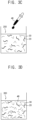
- FIG. 3A , FIG. 3B , FIG. 3C , FIG, 3D , FIG. 3E and FIG. 3F shows process views illustrating a method for forming first, second and third mixing solutions and a method for forming the conductive polymer, in the method for manufacturing the conductive polymer electrode in FIG. 1 .
- IPA isopropyl alcohol
- a conductive material 20 is dispersed in the solution 10, to form a first mixing solution 100 (step S100).
- the conductive material 20 may include carbon nanofiber.
- the conductive material 20 is added to the solution 10, and the conductive material 20 is entirely dispersed in the solution 10 using a vortex mixer.
- the conductive material 20 is additionally dispersed in the solution 10 using an ultrasonic cleaner, for about 100 minutes. Then, the conductive material 20 is uniformly dispersed in the solution 10, and the first mixing solution 100 is formed.
- a predetermined amount of the conductive material 20 is provided to the solution 10 at once and then is dispersed.
- the carbon nanofiber when used as the conductive material 20, the carbon nanofiber may include a nanostructure made of a circular shape graphene having a diameter between about 50 nm and about 200 nm.
- the above carbon nanofiber may have relatively high heat conductivity and high electric conductivity when mixed with a matrix material such as a plastic.
- the carbon nanofiber may include a nanostructure having various kinds of shapes except for the circular shape.
- a first polymer solution 30 is added to the first mixing solution 100 and the first polymer solution 30 is dispersed in the first mixing solution 100, and then a second mixing solution 200 is formed (step S200).
- the first polymer solution 30 is added to the first mixing solution 100, and the first polymer solution 30 is entirely dispersed using the vortex mixer.
- the first polymer solution 30 is additionally dispersed using the ultrasonic cleaner, for about 100 minutes. Then, the first polymer solution 30 is uniformly dispersed in the first mixing solution 100, and the second mixing solution 200 is formed.
- a predetermined amount of the first polymer solution 30 may be provided to the first mixing solution 100 at once, but alternatively, uniform amount of the first polymer solution 30 may be provided to the first mixing solution 100 repeatedly with the same amount and with the same interval.
- the first polymer solution 30 may include EcoFlex 0030 manufactured by Smooth-On Inc., and in the present example embodiment, the first polymer solution 30 may be a monomer type solution.
- a second polymer solution 40 is added to the second mixing solution 200, and the second polymer solution 40 is dispersed in the second mixing solution 200, to form a third mixing solution 300 (step S300).
- the second polymer solution 40 is added to the second mixing solution 200, and the second polymer solution 40 is entirely dispersed using the vortex mixer.
- the second polymer solution 40 is additionally dispersed using the ultrasonic cleaner, for about 100 minutes. Then, the second polymer solution 40 is uniformly dispersed in the second mixing solution 200, and the third mixing solution 300 is formed.
- a predetermined amount of the second polymer solution 40 may be provided to the second mixing solution 200 at once, but alternatively, uniform amount of the second polymer solution 40 may be provided to the second mixing solution 200 repeatedly with the same amount and with the same interval.
- the second polymer solution 40 may include EcoFlex 0030 manufactured by Smooth-On Inc., and in the present example embodiment, the second polymer solution 40 may be a cross-linking agent.
- the third mixing solution 300 in which the conductive material 20, the first polymer solution 30 and the second polymer solution 40 are mixed in the solution 10 is completely manufactured.
- the third mixing solution 300 is dropped on a hot plate using a pipette, which is the drop casting, and thus the solution 10 included in the third mixing solution 300, which is the isopropyl alcohol, is evaporated.
- a conductive polymer is formed (step S400).
- a predetermined amount of third mixing solution 300 is pipetted to be dropped, and thus the third mixing solution 300 is coated on a petri dish (step S410). Then, the petri dish is positioned on a hot plate and is heated for a predetermined time (step S420).
- third mixing solution 300 may be pipetted.
- the petri dish on which the third mixing solution 300 is coated may be heated on the hot plate with a temperature of about 75°C for about 30 minutes.
- step S410 and step S420 are repeated at least five times, and then the conductive polymer 50 having a predetermined thickness may be manufactured, as illustrated in FIG. 3F .
- the drop casting in pipetting the third mixing solution 300 and dropping the third mixing solution 300 on the petri dish, the drop casting is applied so that the third mixing solution 300 may be coated on the petri dish with a constant thickness.
- the third mixing solution 300 may be additionally dropped on the petri dish to be coated on the petri dish by a predetermined thickness, and then the heating and the evaporating may be repeated.
- the third mixing solution 300 is dropped and coated on the petri dish again and the evaporating and the dropping are repeated, until the conductive polymer 50 having the predetermined thickness is manufactured.
- the conductive polymer having the predetermined thickness is coated and formed repeatedly.
- the problem caused in the conventional manufacturing method for the conductive polymer may be solved. That is, in the conventional manufacture method, the heat is provided to relatively large amount of mixing solution at once in the evaporating step without coating the mixing solution on the petri dish by a relatively thin thickness, and thus in the evaporating step, the conductive materials and so on included in the mixing solution are lumped, so that the resistance of the conductive polymer may be increased to decrease the electric characteristics of the conductive polymer.
- an adhesive patch is formed to manufacture the conductive polymer electrode (step S500).
- Sylgard 184 solution is coated on a wafer, and then MG7-9850 solution is coated on the wafer on which the Sylgard 184 solution is coated.
- Sylgard 184 monomer and Sylgard 184 crosslinking agent are mixed with a ratio of 1:1, and a bubble generated in the mixing is removed using a vacuum desiccator.
- the Sylgard 184 solution from which the bubble is removed is spin-coated with the number of revolutions between about 200rpm and about 500rpm on the wafer using a spin-coater, and the wafer is hardened in the hot plate with a temperature of about 120°C for a predetermined time.
- MG7-9850 monomer and MG7-9850 crosslinking agent are mixed with a ratio of 1:1, and a bubble generated in the mixing is removed using the vacuum desiccator.
- the MG7-9850 solution from which the bubble is removed is spin-coated with the number of revolutions between about 200rpm and about 500rpm on the wafer using the spin-coater, and the wafer is hardened in the hot plate with a temperature of about 120°C for a predetermined time.
- the adhesive patch is formed.
- step S600 the adhesive patch is attached to the conductive polymer 50 (step S600).
- the conductive polymer is cut to be fitted to a size of the adhesive patch, for the adhesive patch to cover an entire surface of the conductive polymer 50.
- the adhesive patch entirely covers the conductive polymer and is to be stably attached on a skin.
- Table 1 shows a change of a resistance of the third mixing solution according to the number of drops of the third mixing solution in which the conductive material CNF, the first polymer solution ecoflex A and the second polymer solution ecoflex B.
- Change of resistance according to number of drops IPA [g] CNF [g] ECOFLEX 0030 A [g] ECOFLEX 0030 B [g] 60 1 1.75 1.75 Number of drops 5 times 10 times 15 times 20 times Resistance [k ⁇ ] 20 9 31 29 14 5 54 30 17 7 40 33 24 8 50 54 Mean value 18.75 7.25 43.75 36.5
- the resistance is relatively large in the cases in which the number of the drops is 15 times and 20 times, and the resistance is relatively large in the case in which the number of the drops is 5 times. However, the resistance is relatively small in the case in which the number of the drops is 10 times. Thus, the electric characteristics may be great at the case in which the number of the drops is 10 times.
- Table 2 shows a change of the resistance of the third mixing solution according to a change of the amount of each of the conductive material CNF, the first polymer solution ecoflex A and the second polymer solution ecoflex B, with the constant amount of the solution which is isopropyl alcohol (IPA).
- IPA isopropyl alcohol
- the amount of the isopropyl alcohol is fixed with 30g and the amount of the conductive material is changed with 0.5g and 1g, and thus the ratio between the solution and the conductive material is changed.
- the amount of each of the first and second polymer solutions is changed with 1 time, 1.5 times and 2 times larger than that of the conductive material.
- Example 2 when the amount of each of the first and second polymer solutions is 1.5 times larger than the amount of the conductive material, the electric characteristics are the best, compared to other examples.
- the mixing solution in which the conductive material and the polymer are mixed is dispersed using the drop casting and thus the solution is evaporated.
- the problem such as an increase of an electric resistance generated in the conventional dispersing in which the conductive material and the polymer are lumped may be effectively solved, and the polymer electrode having improved electric characteristics such as conductivity may be easily manufactured.
- the number of the dropping of the mixing solution may be between 5 and 10, and the amount of each of the first polymer solution which is a monomer and the second polymer solution which is a crosslinking agent may be 1.5 times more than the amount of the conductive material, so that the polymer electrode having the enhanced conductivity may be easily manufactured.
Landscapes
- Engineering & Computer Science (AREA)
- Manufacturing & Machinery (AREA)
- Health & Medical Sciences (AREA)
- Life Sciences & Earth Sciences (AREA)
- Organic Chemistry (AREA)
- Chemical & Material Sciences (AREA)
- Molecular Biology (AREA)
- General Health & Medical Sciences (AREA)
- Heart & Thoracic Surgery (AREA)
- Medical Informatics (AREA)
- Pathology (AREA)
- Surgery (AREA)
- Animal Behavior & Ethology (AREA)
- Biomedical Technology (AREA)
- Public Health (AREA)
- Veterinary Medicine (AREA)
- Biophysics (AREA)
- Physics & Mathematics (AREA)
- Compositions Of Macromolecular Compounds (AREA)
- Carbon And Carbon Compounds (AREA)
- Electrodes Of Semiconductors (AREA)
- Processes Of Treating Macromolecular Substances (AREA)
Description
- The present disclosure of invention relates to a method for manufacturing conductive polymer electrode by using drop casting, and more specifically the present invention relates to a method for manufacturing a conductive polymer electrode using a carbon nanofiber and polymer materials via the drop casting.
- In a metal electrode used for a conventional thin-film transistor, a contact interface layer with an organic semiconductor is unstable so that characteristics of a device may be decreased. Thus, to solve the above problem, a study on replacing the conventional metal electrode by an organic electrode has been developed.
- For example, the organic electrodes, such as a conductive polymer like PEDOT/PSS, polyaniline (PANI) polypyrrole (PPy), and so on, carbon nanotube and graphene, have been studied.
-
Korean laid-open patent No. 10-2012-0090594 Korean laid-open patent No. 10-2016-0049555 - However, in the conventional organic electrode, the conductivity decreases as resistance of the organic electrode increases, and thus the quality of the device and the lifespan of the device may be decreased.
- Here, in manufacturing the conductive polymer electrode, the conductive material should be uniformly dispersed in the solution. However, in dispersing the conductive material such as the nanotubes in the solution, the conductive material may be easily lumped due to the high cohesive force, and thus the resistance of the conductive polymer electrode is increased and the electric characteristics of the conductive polymer electrode is decreased.
- Thus, the process for dispersing the conductive material in the solution uniformly should be developed.
- Related prior arts includes
KR 100 745 193 B1KR 2018 0096248 A - The present invention is developed to solve the above-mentioned problems of the related arts. The present invention provides a method for manufacturing a conductive polymer electrode using a drop casting, in which the conductive polymer electrode is manufactured using a carbon nanofiber and polymer materials via a drop casting, so as to increase electric characteristics like electric conductivity.
- According to an example embodiment, in the method for manufacturing a conductive polymer electrode, a conductive material is dispersed in a solution, to form a first mixing solution. A first polymer is added and dispersed to the first mixing solution, to form a second mixing solution. A second polymer solution is added and dispersed to the second mixing solution, to form a third mixing solution. The third mixing solution is dropped on a hot plate using a pipette and a solution of the third mixing solution is evaporated, to form a conductive polymer. The adhesive patch is formed. The adhesive patch is attached to the conductive polymer.
- The solution includes isopropyl alcohol (IPA), and the conductive material includes carbon nanofiber.
- The first polymer solution includes a monomer type solution, and the second polymer solution includes a cross-linking agent.
- In the forming the first mixing solution, the conductive material is added to the solution, the conductive material is dispersed in the solution using a vortex mixer, and the conductive material is dispersed in the solution using a ultrasonic cleaner for a predetermined time.
- In the forming the second mixing solution, the first polymer solution is added to the first mixing solution, the first polymer solution is dispersed in the first mixing solution using a vortex mixer, and the first polymer solution is uniformly dispersed in the first mixing solution using a ultrasonic cleaner for a predetermined time.
- In the forming the third mixing solution, the second polymer solution is added to the second mixing solution, the second polymer solution is dispersed in the second mixing solution using a vortex mixer, and the second polymer solution is uniformly dispersed in the second mixing solution using a ultrasonic cleaner for a predetermined time.
- An amount of each of the first polymer solution and the second polymer solution is 1.5 times more than an amount of the conductive material.
- In an example, the forming the conductive polymer may include pipetting the third mixing solution, to drop the third mixing solution to be coated on a petri dish, and heating the petri dish in the hot plate.
- In an example, the pipetting the third mixing solution and the heating the petri dish may be repeated, to form the conductive polymer having a predetermined thickness
- According to the present example embodiments, the mixing solution in which the conductive material and the polymer are mixed is dispersed using the drop casting and thus the solution is evaporated. Thus, the problem such as an increase of an electric resistance generated in the conventional dispersing in which the conductive material and the polymer are lumped may be effectively solved, and the polymer electrode having improved electric characteristics such as conductivity may be easily manufactured.
- Here, to enhance the electric characteristics such as the conductivity, the number of the dropping of the mixing solution may be between 5 and 10, and the amount of each of the first polymer solution which is a monomer and the second polymer solution which is a crosslinking agent may be 1.5 times more than the amount of the conductive material, so that the polymer electrode having the enhanced conductivity may be easily manufactured.
-
-
FIG. 1 is a flow chart showing a method for manufacturing a conductive polymer electrode using a drop casting according to an example embodiment of the present invention; -
FIG. 2 is a flow chart showing a method for forming a conductive polymer in the method for manufacturing the conductive polymer electrode inFIG. 1 ; and -
FIG. 3A, FIG. 3B ,FIG. 3C, FIG, 3D ,FIG. 3E and FIG. 3F shows process views illustrating a method for forming first, second and third mixing solutions and a method for forming the conductive polymer, in the method for manufacturing the conductive polymer electrode inFIG. 1 . -
20 : conductive material 30 : first polymer solution 40 : second polymer solution 50 : conductive polymer 100 : first mixing solution 200 : second mixing solution 300 : third mixing solution - The invention is described more fully hereinafter with Reference to the accompanying drawings, in which embodiments of the invention are shown. This invention may, however, be embodied in many different forms and should not be construed as limited to the embodiments set forth herein. Rather, these embodiments are provided so that this disclosure will be thorough and complete, and will fully convey the scope of the invention to those skilled in the art. In the drawings, the size and relative sizes of layers and regions may be exaggerated for clarity.
- It will be understood that, although the terms first, second, third etc. may be used herein to describe various elements, components, regions, layers and/or sections, these elements, components, regions, layers and/or sections should not be limited by these terms. These terms are only used to distinguish one element, component, region, layer or section from another region, layer or section. Thus, a first element, component, region, layer or section discussed below could be termed a second element, component, region, layer or section without departing from the teachings of the present invention. Spatially relative terms, such as "beneath," "below," "lower," "above," "upper" and the like, may be used herein for ease of description to describe one element or feature's relationship to another element(s) or feature(s) as illustrated in the figures.
- The terminology used herein is for the purpose of describing particular embodiments only and is not intended to be limiting of the invention. As used herein, the singular forms "a," "an" and "the" are intended to include the plural forms as well, unless the context clearly indicates otherwise. It will be further understood that the terms "comprises" and/or "comprising," when used in this specification, specify the presence of stated features, integers, steps, operations, elements, and/or components, but do not preclude the presence or addition of one or more other features, integers, steps, operations, elements, components, and/or groups thereof. Unless otherwise defined, all terms (including technical and scientific terms) used herein have the same meaning as commonly understood by one of ordinary skill in the art to which this invention belongs.
- It will be further understood that terms, such as those defined in commonly used dictionaries, should be interpreted as having a meaning that is consistent with their meaning in the context of the relevant art and will not be interpreted in an idealized or overly formal sense unless expressly so defined herein.
- The invention is described more fully hereinafter with reference to the accompanying drawings, in which embodiments of the invention are shown.
-
FIG. 1 is a flow chart showing a method for manufacturing a conductive polymer electrode using a drop casting according to an example embodiment of the present invention.FIG. 2 is a flow chart showing a method for forming a conductive polymer in the method for manufacturing the conductive polymer electrode inFIG. 1 .FIG. 3A ,FIG. 3B ,FIG. 3C ,FIG, 3D ,FIG. 3E and FIG. 3F shows process views illustrating a method for forming first, second and third mixing solutions and a method for forming the conductive polymer, in the method for manufacturing the conductive polymer electrode inFIG. 1 . - Referring to
FIG. 1 andFIG. 3A , in the method for manufacturing the conductive polymer electrode using the drop casting according to the present example embodiment, first, isopropyl alcohol (IPA) is used as asolution 10, and aconductive material 20 is dispersed in thesolution 10, to form a first mixing solution 100 (step S100). - Here, the
conductive material 20 may include carbon nanofiber. - For example, the
conductive material 20 is added to thesolution 10, and theconductive material 20 is entirely dispersed in thesolution 10 using a vortex mixer. In addition, after the dispersion using the vortex mixer firstly, theconductive material 20 is additionally dispersed in thesolution 10 using an ultrasonic cleaner, for about 100 minutes. Then, theconductive material 20 is uniformly dispersed in thesolution 10, and thefirst mixing solution 100 is formed. - Here, as illustrated in
FIG. 3A , a predetermined amount of theconductive material 20 is provided to thesolution 10 at once and then is dispersed. - In addition, when the carbon nanofiber is used as the
conductive material 20, the carbon nanofiber may include a nanostructure made of a circular shape graphene having a diameter between about 50 nm and about 200 nm. The above carbon nanofiber may have relatively high heat conductivity and high electric conductivity when mixed with a matrix material such as a plastic. Here, the carbon nanofiber may include a nanostructure having various kinds of shapes except for the circular shape. - Then, referring to
FIG. 1 andFIG. 3B , afirst polymer solution 30 is added to thefirst mixing solution 100 and thefirst polymer solution 30 is dispersed in thefirst mixing solution 100, and then asecond mixing solution 200 is formed (step S200). - For example, the
first polymer solution 30 is added to thefirst mixing solution 100, and thefirst polymer solution 30 is entirely dispersed using the vortex mixer. In addition, after the dispersion using the vortex mixer firstly, thefirst polymer solution 30 is additionally dispersed using the ultrasonic cleaner, for about 100 minutes. Then, thefirst polymer solution 30 is uniformly dispersed in thefirst mixing solution 100, and thesecond mixing solution 200 is formed. - Here, as illustrated in
FIG. 3B , a predetermined amount of thefirst polymer solution 30 may be provided to thefirst mixing solution 100 at once, but alternatively, uniform amount of thefirst polymer solution 30 may be provided to thefirst mixing solution 100 repeatedly with the same amount and with the same interval. - For example, the
first polymer solution 30 may include EcoFlex 0030 manufactured by Smooth-On Inc., and in the present example embodiment, thefirst polymer solution 30 may be a monomer type solution. - Then, referring to
FIG. 1 andFIG. 3C , asecond polymer solution 40 is added to thesecond mixing solution 200, and thesecond polymer solution 40 is dispersed in thesecond mixing solution 200, to form a third mixing solution 300 (step S300). - For example, the
second polymer solution 40 is added to thesecond mixing solution 200, and thesecond polymer solution 40 is entirely dispersed using the vortex mixer. In addition, after the dispersion using the vortex mixer firstly, thesecond polymer solution 40 is additionally dispersed using the ultrasonic cleaner, for about 100 minutes. Then, thesecond polymer solution 40 is uniformly dispersed in thesecond mixing solution 200, and thethird mixing solution 300 is formed. - Here, as illustrated in
FIG. 3C , a predetermined amount of thesecond polymer solution 40 may be provided to thesecond mixing solution 200 at once, but alternatively, uniform amount of thesecond polymer solution 40 may be provided to thesecond mixing solution 200 repeatedly with the same amount and with the same interval. - For example, the
second polymer solution 40 may include EcoFlex 0030 manufactured by Smooth-On Inc., and in the present example embodiment, thesecond polymer solution 40 may be a cross-linking agent. - Then, as illustrated in
FIG. 3D , thethird mixing solution 300 in which theconductive material 20, thefirst polymer solution 30 and thesecond polymer solution 40 are mixed in thesolution 10 is completely manufactured. Then, referring toFIG. 1 andFIG. 3E , thethird mixing solution 300 is dropped on a hot plate using a pipette, which is the drop casting, and thus thesolution 10 included in thethird mixing solution 300, which is the isopropyl alcohol, is evaporated. Then, a conductive polymer is formed (step S400). - Here, in forming the conductive polymer, as illustrated in
FIG. 2 , firstly, a predetermined amount ofthird mixing solution 300 is pipetted to be dropped, and thus thethird mixing solution 300 is coated on a petri dish (step S410). Then, the petri dish is positioned on a hot plate and is heated for a predetermined time (step S420). - For example, 1 mL of
third mixing solution 300 may be pipetted. The petri dish on which thethird mixing solution 300 is coated may be heated on the hot plate with a temperature of about 75°C for about 30 minutes. - The steps (step S410 and step S420) are repeated at least five times, and then the
conductive polymer 50 having a predetermined thickness may be manufactured, as illustrated inFIG. 3F . - In the present example embodiment, in pipetting the
third mixing solution 300 and dropping thethird mixing solution 300 on the petri dish, the drop casting is applied so that thethird mixing solution 300 may be coated on the petri dish with a constant thickness. Thus, after the solution included the droppedthird mixing solution 300 is entirely evaporated as the droppedthird mixing solution 300 is heated on the hot plate, thethird mixing solution 300 may be additionally dropped on the petri dish to be coated on the petri dish by a predetermined thickness, and then the heating and the evaporating may be repeated. - Accordingly, after the
solution 10 included in thethird mixing solution 300 is evaporated from the petri dish on which thethird mixing solution 300 is coated with a uniform thickness, thethird mixing solution 300 is dropped and coated on the petri dish again and the evaporating and the dropping are repeated, until theconductive polymer 50 having the predetermined thickness is manufactured. - Here, using the drop casting, the conductive polymer having the predetermined thickness is coated and formed repeatedly. Thus, the problem caused in the conventional manufacturing method for the conductive polymer may be solved. That is, in the conventional manufacture method, the heat is provided to relatively large amount of mixing solution at once in the evaporating step without coating the mixing solution on the petri dish by a relatively thin thickness, and thus in the evaporating step, the conductive materials and so on included in the mixing solution are lumped, so that the resistance of the conductive polymer may be increased to decrease the electric characteristics of the conductive polymer.
- Further, in addition to manufacturing the conductive polymer, an adhesive patch is formed to manufacture the conductive polymer electrode (step S500).
- In forming the adhesive patch, Sylgard 184 solution is coated on a wafer, and then MG7-9850 solution is coated on the wafer on which the Sylgard 184 solution is coated.
- For example, for coating the Sylgard 184 solution on the wafer, Sylgard 184 monomer and Sylgard 184 crosslinking agent are mixed with a ratio of 1:1, and a bubble generated in the mixing is removed using a vacuum desiccator. In addition, the Sylgard 184 solution from which the bubble is removed is spin-coated with the number of revolutions between about 200rpm and about 500rpm on the wafer using a spin-coater, and the wafer is hardened in the hot plate with a temperature of about 120°C for a predetermined time.
- Then, for coating the MG7-9850 solution on the wafer on which the Sylgard 184 solution is coated, MG7-9850 monomer and MG7-9850 crosslinking agent are mixed with a ratio of 1:1, and a bubble generated in the mixing is removed using the vacuum desiccator. In addition, the MG7-9850 solution from which the bubble is removed is spin-coated with the number of revolutions between about 200rpm and about 500rpm on the wafer using the spin-coater, and the wafer is hardened in the hot plate with a temperature of about 120°C for a predetermined time.
- Thus, the adhesive patch is formed.
- Then, the adhesive patch is attached to the conductive polymer 50 (step S600).
- Here, the conductive polymer is cut to be fitted to a size of the adhesive patch, for the adhesive patch to cover an entire surface of the
conductive polymer 50. Thus, the adhesive patch entirely covers the conductive polymer and is to be stably attached on a skin. - Table 1 shows a change of a resistance of the third mixing solution according to the number of drops of the third mixing solution in which the conductive material CNF, the first polymer solution ecoflex A and the second polymer solution ecoflex B.
[Table 1] Change of resistance according to number of drops IPA [g] CNF [g] ECOFLEX 0030 A [g] ECOFLEX 0030 B [g] 60 1 1.75 1.75 Number of drops 5 times 10 times 15 times 20 times Resistance [kΩ] 20 9 31 29 14 5 54 30 17 7 40 33 24 8 50 54 Mean value 18.75 7.25 43.75 36.5 - Referring to Table 1, the resistance is relatively large in the cases in which the number of the drops is 15 times and 20 times, and the resistance is relatively large in the case in which the number of the drops is 5 times. However, the resistance is relatively small in the case in which the number of the drops is 10 times. Thus, the electric characteristics may be great at the case in which the number of the drops is 10 times.
- Table 2 shows a change of the resistance of the third mixing solution according to a change of the amount of each of the conductive material CNF, the first polymer solution ecoflex A and the second polymer solution ecoflex B, with the constant amount of the solution which is isopropyl alcohol (IPA).
[Table 2] Change of resistance according to change of CNF, ecoflex A and ecoflex B Examples 1 2 3 4 5 6 IPA [g] 30 30 30 30 30 30 CNF [g] 0.5 0.5 0.5 1 1 1 ECOFLEX A [g] 1 0.75 0.5 2 1.5 1 ECOFLEX B [g] 1 0.75 0.5 2 1.5 1 Resistance 109 7 5 129 9 22 [kΩ] 120 7 6 106 9 20 194 5 22 132 7 17 164 5 18 74 10 11 Mean value [kΩ] 147 6 13 110 9 17.5 - Referring to Table 2, the amount of the isopropyl alcohol is fixed with 30g and the amount of the conductive material is changed with 0.5g and 1g, and thus the ratio between the solution and the conductive material is changed. In addition, the amount of each of the first and second polymer solutions is changed with 1 time, 1.5 times and 2 times larger than that of the conductive material.
- Thus, as shown in Example 2 and Example 5, when the amount of each of the first and second polymer solutions is 1.5 times larger than the amount of the conductive material, the electric characteristics are the best, compared to other examples.
- According to the present example embodiments, the mixing solution in which the conductive material and the polymer are mixed is dispersed using the drop casting and thus the solution is evaporated. Thus, the problem such as an increase of an electric resistance generated in the conventional dispersing in which the conductive material and the polymer are lumped may be effectively solved, and the polymer electrode having improved electric characteristics such as conductivity may be easily manufactured.
- Here, to enhance the electric characteristics such as the conductivity, the number of the dropping of the mixing solution may be between 5 and 10, and the amount of each of the first polymer solution which is a monomer and the second polymer solution which is a crosslinking agent may be 1.5 times more than the amount of the conductive material, so that the polymer electrode having the enhanced conductivity may be easily manufactured.
- Although the exemplary embodiments of the present invention have been described, it is understood that the present invention should not be limited to these exemplary embodiments but various changes and modifications can be made by one ordinary skilled in the art.
Claims (3)
- A method for manufacturing a conductive polymer electrode, the method comprising:dispersing a conductive material of carbon nanofiber in a solution of isopropyl alcohol (IPA), to form a first mixing solution;adding and dispersing a first polymer solution being a monomer type solution to the first mixing solution, to form a second mixing solution;adding and dispersing a second polymer solution having a cross-linking agent to the second mixing solution, to form a third mixing solution;dropping the third mixing solution on a hot plate using a pipette and evaporating a solution of the third mixing solution, to form a conductive polymer;forming an adhesive patch; andattaching the adhesive patch to the conductive polymer,wherein an amount of each of the first polymer solution and the second polymer solution is 1.5 times more than an amount of the conductive material,wherein in the forming the first mixing solution, adding the conductive material to the solution, dispersing the conductive material in the solution using a vortex mixer, and dispersing the conductive material in the solution using an ultrasonic cleaner for a predetermined time,wherein in the forming the second mixing solution, adding the first polymer solution to the first mixing solution, dispersing the first polymer solution in the first mixing solution using a vortex mixer, and uniformly dispersing the first polymer solution in the first mixing solution using an ultrasonic cleaner for a predetermined time,wherein in the forming the third mixing solution, adding the second polymer solution to the second mixing solution, dispersing the second polymer solution in the second mixing solution using a vortex mixer, and uniformly dispersing the second polymer solution in the second mixing solution using an ultrasonic cleaner for a predetermined time.
- The method of claim 1, wherein the forming the conductive polymer, comprising:pipetting the third mixing solution, to drop the third mixing solution to be coated on a petri dish; andheating the petri dish in the hot plate.
- The method of claim 1, wherein the pipetting the third mixing solution and the heating the petri dish are repeated, to form the conductive polymer having a predetermined thickness.
Applications Claiming Priority (1)
| Application Number | Priority Date | Filing Date | Title |
|---|---|---|---|
| PCT/KR2019/003933 WO2020204226A1 (en) | 2019-04-03 | 2019-04-03 | Method for preparing conductive polymer electrode by using drop casting |
Publications (3)
| Publication Number | Publication Date |
|---|---|
| EP3923358A1 EP3923358A1 (en) | 2021-12-15 |
| EP3923358A4 EP3923358A4 (en) | 2022-10-12 |
| EP3923358B1 true EP3923358B1 (en) | 2024-05-29 |
Family
ID=72667583
Family Applications (1)
| Application Number | Title | Priority Date | Filing Date |
|---|---|---|---|
| EP19922839.6A Active EP3923358B1 (en) | 2019-04-03 | 2019-04-03 | Method for manufacturing conductive polymer electrode by using drop casting |
Country Status (4)
| Country | Link |
|---|---|
| US (1) | US12364152B2 (en) |
| EP (1) | EP3923358B1 (en) |
| JP (1) | JP7265033B2 (en) |
| WO (1) | WO2020204226A1 (en) |
Family Cites Families (14)
| Publication number | Priority date | Publication date | Assignee | Title |
|---|---|---|---|---|
| JP2004288836A (en) | 2003-03-20 | 2004-10-14 | Toshiba Corp | Organic thin film transistor and method of manufacturing the same |
| WO2006124670A2 (en) | 2005-05-12 | 2006-11-23 | Georgia Tech Research Corporation | Coated metal oxide nanoparticles and methods for producing same |
| US9127174B2 (en) * | 2006-01-20 | 2015-09-08 | Ezaki Glico Co., Ltd. | Aqueous composition for conductive coating |
| KR100745193B1 (en) | 2006-05-30 | 2007-08-01 | 충북대학교 산학협력단 | Method for manufacturing CNP / DAA composite electrode for supercapacitor |
| KR101139927B1 (en) * | 2008-11-10 | 2012-04-30 | 한양대학교 산학협력단 | Method for forming metal oxide semiconductor nanoparticles, polymer electroluminescence device using the metal oxide semiconductor nanoparticles and fabricating the same |
| KR20120090594A (en) | 2011-02-08 | 2012-08-17 | 삼성전자주식회사 | Method of fabricating polymer electrode and polymer actuator employing the polymer electrode |
| JP5952551B2 (en) * | 2011-12-12 | 2016-07-13 | Necトーキン株式会社 | Conductive polymer composition and method for producing the same, method for producing conductive polymer material, method for producing conductive substrate, method for producing electrode, method for producing electronic device, and method for producing solid electrolytic capacitor |
| US20150231610A1 (en) * | 2012-09-04 | 2015-08-20 | National Institute Of Advanced Industrial Science And | Supported gold nanoparticle catalyst and method for producing same |
| KR101696889B1 (en) | 2014-10-01 | 2017-01-18 | 전북대학교산학협력단 | Light Emitting Diodes with Graphene Electrodes and Manufacturing Methods therefore |
| KR101753845B1 (en) | 2015-03-06 | 2017-07-04 | 고려대학교 산학협력단 | Method for preparing conductive polymer composite and conductive polymer composite prepared therefrom |
| KR101719143B1 (en) * | 2015-11-30 | 2017-03-24 | 광주과학기술원 | The method of electrode coated with conducting polymer |
| JP6836520B2 (en) * | 2017-02-14 | 2021-03-03 | 信越化学工業株式会社 | Bioelectrode composition, bioelectrode, and method for producing bioelectrode |
| KR20180096248A (en) * | 2017-02-21 | 2018-08-29 | 영남대학교 산학협력단 | composition forming source-drain electrode of organic thin-film transistor |
| KR102110186B1 (en) * | 2017-12-05 | 2020-05-13 | 재단법인 오송첨단의료산업진흥재단 | Manufacturing method of conductive polymer electrodes using drop casting |
-
2019
- 2019-04-03 EP EP19922839.6A patent/EP3923358B1/en active Active
- 2019-04-03 JP JP2021557575A patent/JP7265033B2/en active Active
- 2019-04-03 WO PCT/KR2019/003933 patent/WO2020204226A1/en not_active Ceased
- 2019-04-03 US US17/437,340 patent/US12364152B2/en active Active
Also Published As
| Publication number | Publication date |
|---|---|
| WO2020204226A1 (en) | 2020-10-08 |
| EP3923358A1 (en) | 2021-12-15 |
| EP3923358A4 (en) | 2022-10-12 |
| US20220149284A1 (en) | 2022-05-12 |
| JP2022527773A (en) | 2022-06-06 |
| JP7265033B2 (en) | 2023-04-25 |
| US12364152B2 (en) | 2025-07-15 |
Similar Documents
| Publication | Publication Date | Title |
|---|---|---|
| Zhang et al. | Tuning the electromechanical properties of PEDOT: PSS films for stretchable transistors and pressure sensors | |
| Zeng et al. | Screen‐printed, low‐cost, and patterned flexible heater based on Ag fractal dendrites for human wearable application | |
| Merlo et al. | Field effect transport and trapping in regioregular polythiophene nanofibers | |
| Lai et al. | Rewritable, moldable, and flexible sticker‐type organic memory on arbitrary substrates | |
| Kim et al. | Self‐compensated insulating ZnO‐based piezoelectric nanogenerators | |
| Kim et al. | Direct writing and aligning of small-molecule organic semiconductor crystals via “dragging mode” electrohydrodynamic jet printing for flexible organic field-effect transistor arrays | |
| Woo et al. | Large‐area CVD‐grown MoS2 driver circuit array for flexible organic light‐emitting diode display | |
| JPWO2010010766A1 (en) | Field effect transistor and circuit device | |
| US20100140600A1 (en) | Thin film transistors incorporating interfacial conductive clusters | |
| TWI581962B (en) | Thermoelectric conversion material and manufacturing method of the same | |
| US20100043708A1 (en) | Ceramic heater, method of manufacturing the same, and apparatus for forming a thin layer having the same | |
| CN1837146A (en) | Thermal interface material and its production method | |
| KR20060064987A (en) | Conductive ink, organic semiconductor transistor using same and manufacturing method thereof | |
| US8696941B2 (en) | Material for functional layer of organic electronic component | |
| Tousignant et al. | N‐Type Single Walled Carbon Nanotube Thin Film Transistors Using Green Tri‐Layer Polymer Dielectric | |
| CN112840002A (en) | Conductive Ink Composition | |
| EP3923358A1 (en) | Method for preparing conductive polymer electrode by using drop casting | |
| Gubanov et al. | C8‐BTBT‐C8 Thin‐Film Transistors Based on Micro‐Contact Printed PEDOT: PSS/MWCNT Electrodes | |
| Wagner et al. | Engineering silver microgrids with a boron nitride nanotube interlayer for highly conductive and flexible transparent heaters | |
| US20140183635A1 (en) | Thin film transistor and method for manufacturing the same | |
| KR102110186B1 (en) | Manufacturing method of conductive polymer electrodes using drop casting | |
| CN108701717B (en) | Thin film transistor, method of manufacturing the same, display panel having the same, and display apparatus having the same | |
| US20130285009A1 (en) | Lateral field emission device | |
| Cha et al. | An all-organic composite system for resistive change memory via the self-assembly of plastic-crystalline molecules | |
| CN102931350A (en) | Solution-processed bipolar thin film transistor and preparation method thereof |
Legal Events
| Date | Code | Title | Description |
|---|---|---|---|
| STAA | Information on the status of an ep patent application or granted ep patent |
Free format text: STATUS: THE INTERNATIONAL PUBLICATION HAS BEEN MADE |
|
| PUAI | Public reference made under article 153(3) epc to a published international application that has entered the european phase |
Free format text: ORIGINAL CODE: 0009012 |
|
| STAA | Information on the status of an ep patent application or granted ep patent |
Free format text: STATUS: REQUEST FOR EXAMINATION WAS MADE |
|
| 17P | Request for examination filed |
Effective date: 20210909 |
|
| AK | Designated contracting states |
Kind code of ref document: A1 Designated state(s): AL AT BE BG CH CY CZ DE DK EE ES FI FR GB GR HR HU IE IS IT LI LT LU LV MC MK MT NL NO PL PT RO RS SE SI SK SM TR |
|
| DAV | Request for validation of the european patent (deleted) | ||
| DAX | Request for extension of the european patent (deleted) | ||
| A4 | Supplementary search report drawn up and despatched |
Effective date: 20220909 |
|
| RIC1 | Information provided on ipc code assigned before grant |
Ipc: H01L 21/02 20060101ALI20220905BHEP Ipc: H01L 21/28 20060101ALI20220905BHEP Ipc: H01L 51/00 20060101ALI20220905BHEP Ipc: H01L 51/10 20060101AFI20220905BHEP |
|
| REG | Reference to a national code |
Ref country code: DE Ref country code: DE Ref legal event code: R079 Ref document number: 602019053104 Country of ref document: DE Free format text: PREVIOUS MAIN CLASS: H01L0051100000 Ipc: H10K0071120000 |
|
| GRAP | Despatch of communication of intention to grant a patent |
Free format text: ORIGINAL CODE: EPIDOSNIGR1 |
|
| STAA | Information on the status of an ep patent application or granted ep patent |
Free format text: STATUS: GRANT OF PATENT IS INTENDED |
|
| RIC1 | Information provided on ipc code assigned before grant |
Ipc: H10K 77/10 20230101ALI20240108BHEP Ipc: H10K 71/60 20230101ALI20240108BHEP Ipc: H10K 71/12 20230101AFI20240108BHEP |
|
| INTG | Intention to grant announced |
Effective date: 20240129 |
|
| GRAS | Grant fee paid |
Free format text: ORIGINAL CODE: EPIDOSNIGR3 |
|
| GRAA | (expected) grant |
Free format text: ORIGINAL CODE: 0009210 |
|
| STAA | Information on the status of an ep patent application or granted ep patent |
Free format text: STATUS: THE PATENT HAS BEEN GRANTED |
|
| AK | Designated contracting states |
Kind code of ref document: B1 Designated state(s): AL AT BE BG CH CY CZ DE DK EE ES FI FR GB GR HR HU IE IS IT LI LT LU LV MC MK MT NL NO PL PT RO RS SE SI SK SM TR |
|
| REG | Reference to a national code |
Ref country code: CH Ref legal event code: EP |
|
| P01 | Opt-out of the competence of the unified patent court (upc) registered |
Effective date: 20240507 |
|
| REG | Reference to a national code |
Ref country code: IE Ref legal event code: FG4D |
|
| REG | Reference to a national code |
Ref country code: DE Ref legal event code: R096 Ref document number: 602019053104 Country of ref document: DE |
|
| REG | Reference to a national code |
Ref country code: LT Ref legal event code: MG9D |
|
| REG | Reference to a national code |
Ref country code: NL Ref legal event code: MP Effective date: 20240529 |
|
| PG25 | Lapsed in a contracting state [announced via postgrant information from national office to epo] |
Ref country code: IS Free format text: LAPSE BECAUSE OF FAILURE TO SUBMIT A TRANSLATION OF THE DESCRIPTION OR TO PAY THE FEE WITHIN THE PRESCRIBED TIME-LIMIT Effective date: 20240929 |
|
| PG25 | Lapsed in a contracting state [announced via postgrant information from national office to epo] |
Ref country code: BG Free format text: LAPSE BECAUSE OF FAILURE TO SUBMIT A TRANSLATION OF THE DESCRIPTION OR TO PAY THE FEE WITHIN THE PRESCRIBED TIME-LIMIT Effective date: 20240529 |
|
| PG25 | Lapsed in a contracting state [announced via postgrant information from national office to epo] |
Ref country code: HR Free format text: LAPSE BECAUSE OF FAILURE TO SUBMIT A TRANSLATION OF THE DESCRIPTION OR TO PAY THE FEE WITHIN THE PRESCRIBED TIME-LIMIT Effective date: 20240529 Ref country code: FI Free format text: LAPSE BECAUSE OF FAILURE TO SUBMIT A TRANSLATION OF THE DESCRIPTION OR TO PAY THE FEE WITHIN THE PRESCRIBED TIME-LIMIT Effective date: 20240529 |
|
| PG25 | Lapsed in a contracting state [announced via postgrant information from national office to epo] |
Ref country code: GR Free format text: LAPSE BECAUSE OF FAILURE TO SUBMIT A TRANSLATION OF THE DESCRIPTION OR TO PAY THE FEE WITHIN THE PRESCRIBED TIME-LIMIT Effective date: 20240830 |
|
| REG | Reference to a national code |
Ref country code: AT Ref legal event code: MK05 Ref document number: 1691702 Country of ref document: AT Kind code of ref document: T Effective date: 20240529 |
|
| PG25 | Lapsed in a contracting state [announced via postgrant information from national office to epo] |
Ref country code: ES Free format text: LAPSE BECAUSE OF FAILURE TO SUBMIT A TRANSLATION OF THE DESCRIPTION OR TO PAY THE FEE WITHIN THE PRESCRIBED TIME-LIMIT Effective date: 20240529 |
|
| PG25 | Lapsed in a contracting state [announced via postgrant information from national office to epo] |
Ref country code: AT Free format text: LAPSE BECAUSE OF FAILURE TO SUBMIT A TRANSLATION OF THE DESCRIPTION OR TO PAY THE FEE WITHIN THE PRESCRIBED TIME-LIMIT Effective date: 20240529 |
|
| PG25 | Lapsed in a contracting state [announced via postgrant information from national office to epo] |
Ref country code: PL Free format text: LAPSE BECAUSE OF FAILURE TO SUBMIT A TRANSLATION OF THE DESCRIPTION OR TO PAY THE FEE WITHIN THE PRESCRIBED TIME-LIMIT Effective date: 20240529 |
|
| PG25 | Lapsed in a contracting state [announced via postgrant information from national office to epo] |
Ref country code: LV Free format text: LAPSE BECAUSE OF FAILURE TO SUBMIT A TRANSLATION OF THE DESCRIPTION OR TO PAY THE FEE WITHIN THE PRESCRIBED TIME-LIMIT Effective date: 20240529 |
|
| PG25 | Lapsed in a contracting state [announced via postgrant information from national office to epo] |
Ref country code: PL Free format text: LAPSE BECAUSE OF FAILURE TO SUBMIT A TRANSLATION OF THE DESCRIPTION OR TO PAY THE FEE WITHIN THE PRESCRIBED TIME-LIMIT Effective date: 20240529 Ref country code: NO Free format text: LAPSE BECAUSE OF FAILURE TO SUBMIT A TRANSLATION OF THE DESCRIPTION OR TO PAY THE FEE WITHIN THE PRESCRIBED TIME-LIMIT Effective date: 20240829 Ref country code: LV Free format text: LAPSE BECAUSE OF FAILURE TO SUBMIT A TRANSLATION OF THE DESCRIPTION OR TO PAY THE FEE WITHIN THE PRESCRIBED TIME-LIMIT Effective date: 20240529 Ref country code: IS Free format text: LAPSE BECAUSE OF FAILURE TO SUBMIT A TRANSLATION OF THE DESCRIPTION OR TO PAY THE FEE WITHIN THE PRESCRIBED TIME-LIMIT Effective date: 20240929 Ref country code: HR Free format text: LAPSE BECAUSE OF FAILURE TO SUBMIT A TRANSLATION OF THE DESCRIPTION OR TO PAY THE FEE WITHIN THE PRESCRIBED TIME-LIMIT Effective date: 20240529 Ref country code: GR Free format text: LAPSE BECAUSE OF FAILURE TO SUBMIT A TRANSLATION OF THE DESCRIPTION OR TO PAY THE FEE WITHIN THE PRESCRIBED TIME-LIMIT Effective date: 20240830 Ref country code: FI Free format text: LAPSE BECAUSE OF FAILURE TO SUBMIT A TRANSLATION OF THE DESCRIPTION OR TO PAY THE FEE WITHIN THE PRESCRIBED TIME-LIMIT Effective date: 20240529 Ref country code: ES Free format text: LAPSE BECAUSE OF FAILURE TO SUBMIT A TRANSLATION OF THE DESCRIPTION OR TO PAY THE FEE WITHIN THE PRESCRIBED TIME-LIMIT Effective date: 20240529 Ref country code: BG Free format text: LAPSE BECAUSE OF FAILURE TO SUBMIT A TRANSLATION OF THE DESCRIPTION OR TO PAY THE FEE WITHIN THE PRESCRIBED TIME-LIMIT Effective date: 20240529 Ref country code: AT Free format text: LAPSE BECAUSE OF FAILURE TO SUBMIT A TRANSLATION OF THE DESCRIPTION OR TO PAY THE FEE WITHIN THE PRESCRIBED TIME-LIMIT Effective date: 20240529 Ref country code: RS Free format text: LAPSE BECAUSE OF FAILURE TO SUBMIT A TRANSLATION OF THE DESCRIPTION OR TO PAY THE FEE WITHIN THE PRESCRIBED TIME-LIMIT Effective date: 20240829 |
|
| PG25 | Lapsed in a contracting state [announced via postgrant information from national office to epo] |
Ref country code: NL Free format text: LAPSE BECAUSE OF FAILURE TO SUBMIT A TRANSLATION OF THE DESCRIPTION OR TO PAY THE FEE WITHIN THE PRESCRIBED TIME-LIMIT Effective date: 20240529 |
|
| PG25 | Lapsed in a contracting state [announced via postgrant information from national office to epo] |
Ref country code: NL Free format text: LAPSE BECAUSE OF FAILURE TO SUBMIT A TRANSLATION OF THE DESCRIPTION OR TO PAY THE FEE WITHIN THE PRESCRIBED TIME-LIMIT Effective date: 20240529 |
|
| PG25 | Lapsed in a contracting state [announced via postgrant information from national office to epo] |
Ref country code: DK Free format text: LAPSE BECAUSE OF FAILURE TO SUBMIT A TRANSLATION OF THE DESCRIPTION OR TO PAY THE FEE WITHIN THE PRESCRIBED TIME-LIMIT Effective date: 20240529 |
|
| PG25 | Lapsed in a contracting state [announced via postgrant information from national office to epo] |
Ref country code: EE Free format text: LAPSE BECAUSE OF FAILURE TO SUBMIT A TRANSLATION OF THE DESCRIPTION OR TO PAY THE FEE WITHIN THE PRESCRIBED TIME-LIMIT Effective date: 20240529 |
|
| PG25 | Lapsed in a contracting state [announced via postgrant information from national office to epo] |
Ref country code: CZ Free format text: LAPSE BECAUSE OF FAILURE TO SUBMIT A TRANSLATION OF THE DESCRIPTION OR TO PAY THE FEE WITHIN THE PRESCRIBED TIME-LIMIT Effective date: 20240529 |
|
| PG25 | Lapsed in a contracting state [announced via postgrant information from national office to epo] |
Ref country code: RO Free format text: LAPSE BECAUSE OF FAILURE TO SUBMIT A TRANSLATION OF THE DESCRIPTION OR TO PAY THE FEE WITHIN THE PRESCRIBED TIME-LIMIT Effective date: 20240529 Ref country code: SK Free format text: LAPSE BECAUSE OF FAILURE TO SUBMIT A TRANSLATION OF THE DESCRIPTION OR TO PAY THE FEE WITHIN THE PRESCRIBED TIME-LIMIT Effective date: 20240529 |
|
| PG25 | Lapsed in a contracting state [announced via postgrant information from national office to epo] |
Ref country code: SM Free format text: LAPSE BECAUSE OF FAILURE TO SUBMIT A TRANSLATION OF THE DESCRIPTION OR TO PAY THE FEE WITHIN THE PRESCRIBED TIME-LIMIT Effective date: 20240529 |
|
| PG25 | Lapsed in a contracting state [announced via postgrant information from national office to epo] |
Ref country code: SM Free format text: LAPSE BECAUSE OF FAILURE TO SUBMIT A TRANSLATION OF THE DESCRIPTION OR TO PAY THE FEE WITHIN THE PRESCRIBED TIME-LIMIT Effective date: 20240529 Ref country code: SK Free format text: LAPSE BECAUSE OF FAILURE TO SUBMIT A TRANSLATION OF THE DESCRIPTION OR TO PAY THE FEE WITHIN THE PRESCRIBED TIME-LIMIT Effective date: 20240529 Ref country code: RO Free format text: LAPSE BECAUSE OF FAILURE TO SUBMIT A TRANSLATION OF THE DESCRIPTION OR TO PAY THE FEE WITHIN THE PRESCRIBED TIME-LIMIT Effective date: 20240529 Ref country code: EE Free format text: LAPSE BECAUSE OF FAILURE TO SUBMIT A TRANSLATION OF THE DESCRIPTION OR TO PAY THE FEE WITHIN THE PRESCRIBED TIME-LIMIT Effective date: 20240529 Ref country code: DK Free format text: LAPSE BECAUSE OF FAILURE TO SUBMIT A TRANSLATION OF THE DESCRIPTION OR TO PAY THE FEE WITHIN THE PRESCRIBED TIME-LIMIT Effective date: 20240529 Ref country code: CZ Free format text: LAPSE BECAUSE OF FAILURE TO SUBMIT A TRANSLATION OF THE DESCRIPTION OR TO PAY THE FEE WITHIN THE PRESCRIBED TIME-LIMIT Effective date: 20240529 |
|
| PG25 | Lapsed in a contracting state [announced via postgrant information from national office to epo] |
Ref country code: IT Free format text: LAPSE BECAUSE OF FAILURE TO SUBMIT A TRANSLATION OF THE DESCRIPTION OR TO PAY THE FEE WITHIN THE PRESCRIBED TIME-LIMIT Effective date: 20240529 |
|
| REG | Reference to a national code |
Ref country code: DE Ref legal event code: R097 Ref document number: 602019053104 Country of ref document: DE |
|
| PLBE | No opposition filed within time limit |
Free format text: ORIGINAL CODE: 0009261 |
|
| STAA | Information on the status of an ep patent application or granted ep patent |
Free format text: STATUS: NO OPPOSITION FILED WITHIN TIME LIMIT |
|
| PG25 | Lapsed in a contracting state [announced via postgrant information from national office to epo] |
Ref country code: SI Free format text: LAPSE BECAUSE OF FAILURE TO SUBMIT A TRANSLATION OF THE DESCRIPTION OR TO PAY THE FEE WITHIN THE PRESCRIBED TIME-LIMIT Effective date: 20240529 |
|
| PGFP | Annual fee paid to national office [announced via postgrant information from national office to epo] |
Ref country code: GB Payment date: 20250314 Year of fee payment: 7 |
|
| 26N | No opposition filed |
Effective date: 20250303 |
|
| PGFP | Annual fee paid to national office [announced via postgrant information from national office to epo] |
Ref country code: DE Payment date: 20250428 Year of fee payment: 7 |
|
| PGFP | Annual fee paid to national office [announced via postgrant information from national office to epo] |
Ref country code: FR Payment date: 20250424 Year of fee payment: 7 |
|
| PG25 | Lapsed in a contracting state [announced via postgrant information from national office to epo] |
Ref country code: SE Free format text: LAPSE BECAUSE OF FAILURE TO SUBMIT A TRANSLATION OF THE DESCRIPTION OR TO PAY THE FEE WITHIN THE PRESCRIBED TIME-LIMIT Effective date: 20240529 |
|
| REG | Reference to a national code |
Ref country code: CH Ref legal event code: H13 Free format text: ST27 STATUS EVENT CODE: U-0-0-H10-H13 (AS PROVIDED BY THE NATIONAL OFFICE) Effective date: 20251125 |
|
| PG25 | Lapsed in a contracting state [announced via postgrant information from national office to epo] |
Ref country code: LU Free format text: LAPSE BECAUSE OF NON-PAYMENT OF DUE FEES Effective date: 20250403 |
|
| PG25 | Lapsed in a contracting state [announced via postgrant information from national office to epo] |
Ref country code: MC Free format text: LAPSE BECAUSE OF FAILURE TO SUBMIT A TRANSLATION OF THE DESCRIPTION OR TO PAY THE FEE WITHIN THE PRESCRIBED TIME-LIMIT Effective date: 20240529 |
|
| REG | Reference to a national code |
Ref country code: BE Ref legal event code: MM Effective date: 20250430 |
|
| PG25 | Lapsed in a contracting state [announced via postgrant information from national office to epo] |
Ref country code: BE Free format text: LAPSE BECAUSE OF NON-PAYMENT OF DUE FEES Effective date: 20250430 |
|
| PG25 | Lapsed in a contracting state [announced via postgrant information from national office to epo] |
Ref country code: CH Free format text: LAPSE BECAUSE OF NON-PAYMENT OF DUE FEES Effective date: 20250430 |
|
| PG25 | Lapsed in a contracting state [announced via postgrant information from national office to epo] |
Ref country code: IE Free format text: LAPSE BECAUSE OF NON-PAYMENT OF DUE FEES Effective date: 20250403 |