EP3923290A1 - Write operation circuit, semiconductor memory, and write operation method - Google Patents
Write operation circuit, semiconductor memory, and write operation method Download PDFInfo
- Publication number
- EP3923290A1 EP3923290A1 EP20879711.8A EP20879711A EP3923290A1 EP 3923290 A1 EP3923290 A1 EP 3923290A1 EP 20879711 A EP20879711 A EP 20879711A EP 3923290 A1 EP3923290 A1 EP 3923290A1
- Authority
- EP
- European Patent Office
- Prior art keywords
- data
- input
- inversion flag
- global bus
- input data
- Prior art date
- Legal status (The legal status is an assumption and is not a legal conclusion. Google has not performed a legal analysis and makes no representation as to the accuracy of the status listed.)
- Granted
Links
Images


Classifications
-
- G—PHYSICS
- G11—INFORMATION STORAGE
- G11C—STATIC STORES
- G11C11/00—Digital stores characterised by the use of particular electric or magnetic storage elements; Storage elements therefor
- G11C11/21—Digital stores characterised by the use of particular electric or magnetic storage elements; Storage elements therefor using electric elements
- G11C11/34—Digital stores characterised by the use of particular electric or magnetic storage elements; Storage elements therefor using electric elements using semiconductor devices
- G11C11/40—Digital stores characterised by the use of particular electric or magnetic storage elements; Storage elements therefor using electric elements using semiconductor devices using transistors
- G11C11/401—Digital stores characterised by the use of particular electric or magnetic storage elements; Storage elements therefor using electric elements using semiconductor devices using transistors forming cells needing refreshing or charge regeneration, i.e. dynamic cells
- G11C11/4063—Auxiliary circuits, e.g. for addressing, decoding, driving, writing, sensing or timing
- G11C11/407—Auxiliary circuits, e.g. for addressing, decoding, driving, writing, sensing or timing for memory cells of the field-effect type
- G11C11/409—Read-write [R-W] circuits
-
- G—PHYSICS
- G11—INFORMATION STORAGE
- G11C—STATIC STORES
- G11C7/00—Arrangements for writing information into, or reading information out from, a digital store
- G11C7/10—Input/output [I/O] data interface arrangements, e.g. I/O data control circuits, I/O data buffers
- G11C7/1048—Data bus control circuits, e.g. precharging, presetting, equalising
-
- G—PHYSICS
- G11—INFORMATION STORAGE
- G11C—STATIC STORES
- G11C7/00—Arrangements for writing information into, or reading information out from, a digital store
- G11C7/10—Input/output [I/O] data interface arrangements, e.g. I/O data control circuits, I/O data buffers
- G11C7/1015—Read-write modes for single port memories, i.e. having either a random port or a serial port
- G11C7/1039—Read-write modes for single port memories, i.e. having either a random port or a serial port using pipelining techniques, i.e. using latches between functional memory parts, e.g. row/column decoders, I/O buffers, sense amplifiers
-
- G—PHYSICS
- G11—INFORMATION STORAGE
- G11C—STATIC STORES
- G11C11/00—Digital stores characterised by the use of particular electric or magnetic storage elements; Storage elements therefor
- G11C11/21—Digital stores characterised by the use of particular electric or magnetic storage elements; Storage elements therefor using electric elements
- G11C11/34—Digital stores characterised by the use of particular electric or magnetic storage elements; Storage elements therefor using electric elements using semiconductor devices
- G11C11/40—Digital stores characterised by the use of particular electric or magnetic storage elements; Storage elements therefor using electric elements using semiconductor devices using transistors
- G11C11/401—Digital stores characterised by the use of particular electric or magnetic storage elements; Storage elements therefor using electric elements using semiconductor devices using transistors forming cells needing refreshing or charge regeneration, i.e. dynamic cells
- G11C11/4063—Auxiliary circuits, e.g. for addressing, decoding, driving, writing, sensing or timing
- G11C11/407—Auxiliary circuits, e.g. for addressing, decoding, driving, writing, sensing or timing for memory cells of the field-effect type
- G11C11/409—Read-write [R-W] circuits
- G11C11/4096—Input/output [I/O] data management or control circuits, e.g. reading or writing circuits, I/O drivers or bit-line switches
-
- G—PHYSICS
- G11—INFORMATION STORAGE
- G11C—STATIC STORES
- G11C7/00—Arrangements for writing information into, or reading information out from, a digital store
- G11C7/10—Input/output [I/O] data interface arrangements, e.g. I/O data control circuits, I/O data buffers
- G11C7/1006—Data managing, e.g. manipulating data before writing or reading out, data bus switches or control circuits therefor
-
- G—PHYSICS
- G11—INFORMATION STORAGE
- G11C—STATIC STORES
- G11C7/00—Arrangements for writing information into, or reading information out from, a digital store
- G11C7/10—Input/output [I/O] data interface arrangements, e.g. I/O data control circuits, I/O data buffers
- G11C7/1051—Data output circuits, e.g. read-out amplifiers, data output buffers, data output registers, data output level conversion circuits
- G11C7/1057—Data output buffers, e.g. comprising level conversion circuits, circuits for adapting load
-
- G—PHYSICS
- G11—INFORMATION STORAGE
- G11C—STATIC STORES
- G11C7/00—Arrangements for writing information into, or reading information out from, a digital store
- G11C7/10—Input/output [I/O] data interface arrangements, e.g. I/O data control circuits, I/O data buffers
- G11C7/1051—Data output circuits, e.g. read-out amplifiers, data output buffers, data output registers, data output level conversion circuits
- G11C7/1063—Control signal output circuits, e.g. status or busy flags, feedback command signals
-
- G—PHYSICS
- G11—INFORMATION STORAGE
- G11C—STATIC STORES
- G11C7/00—Arrangements for writing information into, or reading information out from, a digital store
- G11C7/10—Input/output [I/O] data interface arrangements, e.g. I/O data control circuits, I/O data buffers
- G11C7/1078—Data input circuits, e.g. write amplifiers, data input buffers, data input registers, data input level conversion circuits
- G11C7/1084—Data input buffers, e.g. comprising level conversion circuits, circuits for adapting load
-
- G—PHYSICS
- G11—INFORMATION STORAGE
- G11C—STATIC STORES
- G11C7/00—Arrangements for writing information into, or reading information out from, a digital store
- G11C7/10—Input/output [I/O] data interface arrangements, e.g. I/O data control circuits, I/O data buffers
- G11C7/1078—Data input circuits, e.g. write amplifiers, data input buffers, data input registers, data input level conversion circuits
- G11C7/109—Control signal input circuits
-
- G—PHYSICS
- G11—INFORMATION STORAGE
- G11C—STATIC STORES
- G11C2207/00—Indexing scheme relating to arrangements for writing information into, or reading information out from, a digital store
- G11C2207/10—Aspects relating to interfaces of memory device to external buses
- G11C2207/107—Serial-parallel conversion of data or prefetch
Definitions
- This application relates to the technical field of semiconductor memories, and in particular to a write operation circuit, a semiconductor memory, and a write operation method.
- Semiconductor memories include static random access memory (SRAM), dynamic random access memory (DRAM), synchronous dynamic random access memory (SDRAM), Read-Only Memory (ROM), flash memory, and so on.
- SRAM static random access memory
- DRAM dynamic random access memory
- SDRAM synchronous dynamic random access memory
- ROM Read-Only Memory
- Embodiments of the present application provide a write operation circuit, a semiconductor memory, and a write operation method to solve or alleviate one or more technical problems in the prior art.
- an embodiment of the present application provides a write operation circuit applied to a semiconductor memory, the write operation circuit including:
- a data determination module configured to determine, according to a number of high data bits in input data of the semiconductor memory, whether to invert the input data to generate inversion flag data and first intermediate data
- a data buffer module that includes a plurality of P-channel Metal Oxide Semiconductor (PMOS) transistors and a plurality of first inverters, where the gate of the PMOS transistor is coupled to the data determination module through the first inverter for receiving a second intermediate data, the drain of the PMOS transistor is coupled to a global Bus, the data buffer module being used to determine whether to invert the global bus according to the second intermediate data, where the second intermediate data is an inverted data of the first intermediate data;
- PMOS Metal Oxide Semiconductor
- serial-to-parallel conversion circuit that is coupled between a Data Queue (DQ) port of the semiconductor memory and the data determination module, and that is configured to perform serial-to-parallel conversion on the first input data of the DQ port to generate second input data, where the data determination module is used for determining whether to invert the second input data according to the number of high data bits in the second input data, so as to generate the inversion flag data and the first intermediate data.
- DQ Data Queue
- the second input data is divided into a number of M sets
- the inversion flag data includes a number of M bits
- the M-bit inversion flag data being in one-to-one correspondence with the M sets of second input data.
- Each set of second input data includes a number of N bits, where M and N are integers greater than 1.
- the data determination module is used for outputting the inverted data of the set of second input data as the corresponding set of first intermediate data, and setting the data bit in the inversion flag data corresponding to the set of second input data to high.
- the data determination module is used for outputting the set of second input data as the corresponding set of first intermediate data, and setting the data bit in the inversion flag data corresponding to the set of second input data to low.
- the data determination module includes:
- the data selector includes a plurality of data selection units, the data selection unit including:
- the global bus data includes M sets of global bus data
- the M-bit inversion flag data corresponds to the M sets of global bus data in one-to-one correspondence.
- the data receiving module includes a number of M data receiving units coupled to the memory banks, where the data receiving unit is used to decode the global bus data of the corresponding set according to the one-bit inversion flag data.
- the data receiving unit includes:
- the precharge module includes a plurality of NMOS transistors and a plurality of hold circuits, where the gate of the NMOS transistor is coupled to a precharge signal line, the drain of the NMOS transistor is coupled to the global bus, and the input and output ends of the hold circuit are coupled to the global bus.
- an embodiment of the present application provides a semiconductor memory including the write operation circuit according to any of the foregoing embodiments.
- an embodiment of the present application provides a write operation method applied to a semiconductor memory, the write operation method including:
- the operation of determining, according to a number of high data bits in input data of the semiconductor memory, whether to invert the input data to generate inversion flag data and first intermediate data includes:
- the operation of determining whether to invert the second input data based on the number of high data bits in the second input data so as to generate the inversion flag data and the first intermediate data includes:
- embodiments of the present application can reduce the number of inversions on the global bus under the precharge pull-down architecture, thereby greatly compressing the current and reducing the power consumption.
- FIG. 1 schematically shows a block diagram of a part of the structure of a semiconductor memory according to an embodiment of the present application.
- the semiconductor memory 20 includes a DQ port 24, a memory bank (bank) 26, and a write operation circuit.
- the write operation circuit includes a global bus (Global Bus), an inversion flag (identification) signal line, a serial-to-parallel conversion circuit 21, a data determination module 23, a data buffer module (Data Bus Buffer) 22, a data receiving module 25, and a precharge module 27.
- the semiconductor memory 20 is a DRAM, such as a fourth-generation double-rate synchronous dynamic random access memory (Double Data Rate SDRAM 4, DDR4 for short).
- a 8-bit first input data DQ ⁇ 7:0> is input from the DQ port 24, so that the data to be written (namely the decoded data) D ⁇ 127:0 would be written into the memory bank 26 through the write operation circuit.
- One Active command turns on one unique designated memory bank 26, and the write operation can only be performed on one memory bank 26. In other words, when one of the eight memory banks 26 (i.e. Bank ⁇ 7:0>) is operating, the other Banks are not operating. It should be noted, however, that the number of memory banks 26, the number of data bits of each memory bank 26, the number of the DQ ports 24 and the number of data bits of the DQ ports 24 will not be limited in the embodiment.
- each DQ port 24 is used to input a 8-bit first input data
- a write operation is performed on a set of memory banks Bank ⁇ 7:0> by writing the first input data DQ ⁇ 7:0> through the above-mentioned write operation circuit; a write operation is performed on another set of memory banks Bank ⁇ 15:8> by writing the first input data DQ ⁇ 15:8> through the above-mentioned another write operation circuit. Accordingly, among the eight memory banks 26 corresponding to DQ ⁇ 15:8> (i.e. Bank ⁇ 15:8>), when only one bank operates, the other banks do not operate.
- the semiconductor memory 20 has an array structure, and different units may have the same structure. However, because the input data are different, the output data of different units may be different.
- the following takes one memory bank as an example to introduce the write operation circuit of the embodiment.
- the write operation circuit of the embodiment includes a data determination module 23, which is used to determine, according to the number of high data bits in the input data of the semiconductor memory 20, whether to invert the input data so as to generate inversion flag data and first intermediate data.
- the data determination module 23 is configured to output the inverted data of the input data as the first intermediate data in the case where the number of high data bits in the input data is greater than the preset value, and set the Flag data to high, and output the original input data as the first intermediate data in the case where the number of high data bits in the input data is less than or equal to the preset value, and set the Flag data to low.
- a "high” data bit may mean a data bit that is equal to “1”, while a “low” data bit may be a data bit that is equal to "0".
- Data inversion can be understood as changing from “0” to “1”, or from “1” to “0".
- the inversion of the data line or the signal line may be understood as changing a high level to a low level, or changing a low level to a high level.
- the write operation circuit includes a serial-to-parallel conversion circuit 21.
- the serial-to-parallel conversion circuit 21 is coupled between the DQ port 24 and the data determination module 24, and is used to perform serial-to-parallel conversion on the first input data of the DQ port 24 so as to generate second input data.
- the serial-to-parallel conversion circuit 21 performs serial-to-parallel conversion on the 8-bit first input data DQ ⁇ 7:0>, thus generating a 128-bit second input data D2' ⁇ 127:0> corresponding to Bank0.
- the second input data D2' ⁇ 127:0> is divided into M sets
- the Flag data has M bits, which have one-to-one correspondence relationship with the M sets of second input data
- each set of second input data has N bits, where M and N are integers greater than 1.
- the data determination module 23 is used for outputting the inverted data of the set of second input data as the corresponding set of first intermediate data, and setting the data bit in the inversion flag data corresponding to the set of second input data to high.
- the data determination module is used for outputting the set of second input data as the corresponding set of first intermediate data, and setting the data bit in the inversion flag data corresponding to the set of second input data to low.
- the second input data D2' ⁇ 127:0> is divided into 16 sets, where each set of second input data has 8 bits, and each set of second input data corresponds to one bit of the Flag data.
- the Flag data has 16 bits, such as Flag ⁇ 15:0>.
- the first intermediate data D1' ⁇ 127:0> will be divided into 16 sets accordingly. Each bit of Flag data corresponds to a set of first intermediate data.
- the semiconductor memory 20 of the embodiment further includes a data buffer module 22 and a precharge module 27.
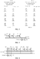
- FIG. 3 schematically shows a circuit diagram (corresponding to one memory bank 26) of a data buffer module 22 according to an embodiment of the present application.
- FIG. 4 schematically shows a circuit diagram (corresponding to 8 memory banks 26) of a data buffer module 22 according to an embodiment of the present application.
- the data buffer module 22 includes a plurality of PMOS (Positive Channel Metal Oxide Semiconductor) transistors 221 and a plurality of first inverters 24.
- the gate of the PMOS transistor 221 is coupled to the data determination module 23 through the first inverter 24, and the drain of the PMOS transistor 221 is coupled to the global bus.
- the first inverter 24 is used to perform an inversion operation on the first intermediate data to generate the second intermediate data, so that the data buffer module 22 further determines whether to invert the global bus according to the second intermediate data. Since there are relatively more data bits of "0" in the first intermediate data, there are relatively more data bits of "1" in the second intermediate data.
- the precharge module 27 is coupled to the precharge signal line (Precharge), and is used to set the initial state of the global bus to low. That is to say, in the embodiment, the semiconductor memory 20 adopts a precharge pull-down (Low) global bus transfer structure.
- the precharge module 27 includes a plurality of NMOS (Negative Channel Metal Oxide Semiconductor) transistors 222 and a plurality of hold circuits 223.
- the gate of the NMOS transistor 222 is coupled to the precharge signal line, and the drain of the NMOS transistor 222 is coupled to the global bus.
- the input and output ends of the hold circuit 223 are coupled to the global bus, thereby forming a positive feedback circuit.
- the Precharge serves the function of setting the initial state of each global bus to low.
- the specific process includes generating a pull-down pulse (pulse, lasting about 2ns) by the Precharge signal, thus pulling down the corresponding global bus for a while.
- the hold circuit 223 then forms a positive feedback and locks the global bus at low level, but the ability of the hold circuit 223 to pull up and pull down current is relatively weak.
- the data line corresponding to the global bus (that is, the data line coupled to the gate of the PMOS transistor 221 corresponding to this global bus) is pulled down for a bit (also a pulse, lasting about 2ns), so that the corresponding PMOS transistor 221 will pull up the global bus for a while (the pull-up capability is greater than the pull-down capability of the hold circuit 223). Then the global bus will be locked to a high level through positive feedback to complete the inversion action of the data line. Since there are relatively more data bits "0" in the second intermediate data, relatively fewer inversion actions are required. Therefore, the IDD4W (write current) of the semiconductor memory will be reduced, thereby reducing the power consumption of the semiconductor memory.
- each global bus transfers one bit of the global bus data.
- M is an integer greater than 1
- each global bus transfers one bit of the global bus data.
- 128 global buses where global bus ⁇ 0> transfers global bus data D' ⁇ 0>, global bus ⁇ 1> transfers global bus data D' ⁇ 1>; whil, global bus ⁇ 127> transfers global bus data D' ⁇ 127>.
- the 128 global buses are divided into 16 sets.
- each bit of Flag data corresponds to a set of global bus data.
- the Flag data has 16 bits, such as Flag ⁇ 15:0>.
- Each Flag signal line transfers 1 bit of Flag data.
- Flag signal line ⁇ 0> transfers Flag data Flag ⁇ 0>, and corresponds to the global bus data D' ⁇ 0:7>, indicating whether D' ⁇ 0:7> is the inverted data of the second intermediate data.
- the Flag signal line ⁇ 1> transfers Flag data Flag ⁇ 1>, and corresponds to the global bus data D' ⁇ 8:15>, indicating whether D' ⁇ 8:15> is the inverted data of the second intermediate data, and so on and so forth...., until the Flag signal line ⁇ 15> transfers Flag data Flag ⁇ 15>, and corresponds to the global bus data D' ⁇ 120:127>, indicating whether D' ⁇ 120:127> is the inverted data of the second intermediate data.
- the second intermediate data is the inverted data of the first intermediate data D1' ⁇ 120:127>
- the global bus data D' ⁇ 127:120> D1' ⁇ 127:120 >.
- the global bus data D' ⁇ 127:120> is the inverted data of D1' ⁇ 127:120>.
- the 256-bit global bus data (including the 128-bit global bus data corresponding to DQ ⁇ 7:0> and the 128-bit global bus data corresponding to DQ ⁇ 15:8>), there are relatively more data bits of "0".
- the data determination module 230 includes a data determination unit 231 and a data selector 232.
- the input end of the data determination unit 231 is coupled to the serial-to-parallel conversion circuit 21, and the output end of the data determination unit 231 is coupled to the Flag signal line, and is further coupled to the input end of the data selector 232.
- the data determination unit 231 is configured to set the Flag data to high in the case where the number of high data bits in the second input data is greater than the preset value, and set the Flag data to low in the case where the number of high data bits in the second input data is less than or equal to the preset value.
- the input end of the data selector 232 is coupled to the data determination unit 231 for receiving the second input data through the data determination unit 231.
- the input end of the data selector 232 also receives the Flag data through the Flag signal line, and the output end of the data selector 232 is coupled to the input end of the first inverter 224.
- the data selector 232 is used to output the inverted data of the second input data as the first intermediate data in the case where the Flag data is high, and use the original second input data as the first intermediate data in the case where the Flag data is high.
- the data selector 232 includes a plurality of data selection units 232', where each data selection unit 232' is used to process one bit of Flag data and a set of second input data. For example, there may be 16 data selection units 232', corresponding to respective 16 sets of second input data and one bit of Flag data.
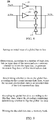
- FIG. 6 shows an implementation of the data selection unit 232'.
- the data selection unit 232' includes a second inverter 232A, a third inverter 232B, a first transmission gate 232C, and a second transmission gate 232D.
- the input end of the second inverter 232A receives Flag data through the Flag signal line.
- the input end of the third inverter 232B is coupled to the data determination unit 231 for receiving the second input data from the data determination unit 231.
- the input end of the first transmission gate 232C is coupled to the output end of the third inverter 232B.
- the output end of the first transmission gate 232C is coupled to the input end of the first inverter 224 for outputting the first intermediate data.
- the negative control end of the first transmission gate 232C (the upper control end shown in FIG. 6 ) is coupled to the output end of the second inverter 232A.
- the positive control end of the first transmission gate 232C receives the Flag data through the Flag signal line.
- the input end of the second transmission gate 232D is coupled to the data determination unit 231 for receiving the second input data from the data determination unit 231.
- the output end of the second transmission gate 232D is coupled to the input end of the first inverter 224 for outputting the first intermediate data.
- the negative control end of the second transmission gate 232D receives the Flag data through the Flag signal line.
- the positive control end of the second transmission gate 232D is coupled to the output end of the second inverter 232A.
- one set of the third inverter 232B, first transmission gate 232C and second transmission gate 232D are used to process one bit of the second input data and output one bit of the corresponding first intermediate data.
- the global bus data D' ⁇ 127:0> is the inverted data of the second input data D2' ⁇ 127:0>.
- the global bus data D' ⁇ 127:0> is the original second input data D2' ⁇ 127:0>.
- the write operation circuit in the embodiment further includes a data receiving module 25.
- the input end of the data receiving module 25 is coupled to the global bus and to the inversion flag signal line.
- the output end of the data receiving module 25 is coupled to the memory bank 26.
- the data receiving module 25 is used to determine whether to invert the global bus data (decoding the global bus data) according to the Flag data, and write the decoded data (write data) into the memory bank 26. For example, in the case where the Flag data is high, the inverted data of the global bus data is output as the data to be written; and when the Flag data is low, the original global bus data is output as the data to be written.
- the written data is restored to the input data of the semiconductor memory. Accordingly, the data and functions of the external ports of the semiconductor memory 20, such as the DQ port 24 and the DBI port (not shown in the figures), will not be changed.
- the data receiving module 25 may include a plurality of data receiving units 250, where each data receiving unit 250 is used to process one bit of Flag data and a set of global bus data. For example, there may be 16 data receiving units 250, corresponding to respective 16 sets of global bus data and one bit of Flag data.
- FIG. 8 shows an implementation of the data receiving unit 250.
- the data receiving unit 250 includes a fourth inverter 251, a fifth inverter 252, a third transmission gate 253, and a fourth transmission gate 254.
- the input end of the fourth inverter 251 receives the Flag data through the Flag signal line.
- the input end of the fifth inverter 252 receives the global bus data through the global bus.
- the input end of the third transmission gate 253 is coupled to the output end of the fifth inverter 252.
- the output end of the third transmission gate 253 is coupled to the memory bank 26 for outputting data to be written into the memory bank 26.
- the negative control end of the third transmission gate 253 (the upper control end shown in FIG. 8 ) is coupled to the output end of the third inverter 251.
- the positive control end of the third transmission gate 253 receives the Flag data through the Flag signal line.
- the input end of the fourth transmission gate 254 receives the global bus data through the global bus.
- the output end of the fourth transmission gate 254 is coupled to the memory bank 26 for outputting data to be written into the memory bank 26.
- the negative control end (the upper control end shown in FIG. 8 ) of the fourth transmission gate 254 receives Flag data through the Flag signal line, and the positive control end (the lower control end shown in FIG. 8 ) of the fourth transmission gate 254 is coupled to the output end of the fourth inverter 251.
- one set of the fifth inverter 252, third transmission gate 253, and fourth transmission gate 254 are used to process one bit of global bus data and output one bit of corresponding written data.
- the global bus data is 256 bits, so if there is a need to invert 256-bit global bus data, it will turn out that only the 32-bit Flag data will be inverted, so that the IDD4W will be greatly compressed.
- the semiconductor memory 20 of the embodiment further includes other structures such as a sense amplifier, a precharge circuit, etc. in practical applications, which are all existing technologies and so are not repeatedly detailed in the embodiment for brevity.
- FIG. 9 schematically shows a flowchart of a write operation method according to an embodiment of the present application.
- This writing operation method can be applied to the semiconductor memory 20 described above.
- the write operation method may include the following operations:
- operation S902 may include: performing serial-to-parallel conversion on the first input data of the DQ port to generate the second input data; and determining whether or not to invert the second input data according to the number of high data bits in the second input data, so as to generate the inversion flag data and the first intermediate data.
- the operation of determining whether or not to invert the second input data according to the number of high data bits in the second input data, so as to generate the inversion flag data and the first intermediate data include: dividing the second input data into M sets, where each set of second input data has N bits; in the case where the number of high data bits in one input set of second input data is greater than N/2, outputting the inverted data of the set of second input data as the corresponding set of first intermediate data, and setting the data bit in the inversion flag data corresponding to the set of second input data to high; and in the case where the number of high data bits in one input set of second input data is less than or equal to N/2, outputting the set of second input data as the corresponding set of first intermediate data, and setting the data bit in the inversion flag data corresponding to the set of second input data to low.
- the write operation circuit provided by the embodiment of the present application can be applied to a semiconductor memory with a global bus transfer structure of the precharge pull-down type, which can reduce the number of internal global bus inversions before data is written into the memory block, thus greatly compressing the current and reducing the power consumption.
- references to the terms “one embodiment”, “some embodiments”, “examples”, “specific examples”, or “some examples” etc. are intended to mean that specific features, structures, materials, or characteristics described in connection with the embodiment or example are included in at least one embodiment or example of the present application. Furthermore, the described specific features, structures, materials or characteristics can be combined in any one or more embodiments or examples in a suitable manner. In addition, those having ordinary skill in the art may be able to combine the different embodiments or examples and the features of the different embodiments or examples described in this specification, in the premise that no contradiction or conflict is present.
- first, second, or the like are merely used for illustrative purposes, and shall not be construed as indicating relative importance or implicitly indicating the number of technical features specified. Thus, the features defined by “first” and “second” may explicitly or implicitly include one or more of such features. As used herein, terms “multiple” or “a plurality of' means two or more, unless otherwise specifically defined.
Landscapes
- Engineering & Computer Science (AREA)
- Microelectronics & Electronic Packaging (AREA)
- Computer Hardware Design (AREA)
- Databases & Information Systems (AREA)
- Dram (AREA)
Abstract
Description
- This application claims the priority to and benefit of
Chinese patent application number 201911021470.5, entitled "Write Operation Circuit, Semiconductor Memory, and Write Operation Method", and filed on October 25, 2019 - This application relates to the technical field of semiconductor memories, and in particular to a write operation circuit, a semiconductor memory, and a write operation method.
- This section is intended to provide background or context for the embodiments of the application defined in the appended claims. Thus, the description of this section is not to be interpreted as prior art for the mere fact of being included in this section.
- Semiconductor memories include static random access memory (SRAM), dynamic random access memory (DRAM), synchronous dynamic random access memory (SDRAM), Read-Only Memory (ROM), flash memory, and so on.
- In the DRAM protocol of the Joint Electron Device Engineering Council (JEDEC), there are specific speed and power saving requirements for DRAM. It therefore has become an urgent problem to be solved as to make DRAM more power-saving while also ensuring signal integrity and reliability of data transfer and storage.
- Embodiments of the present application provide a write operation circuit, a semiconductor memory, and a write operation method to solve or alleviate one or more technical problems in the prior art.
- In a first aspect, an embodiment of the present application provides a write operation circuit applied to a semiconductor memory, the write operation circuit including:
- a data determination module configured to determine, according to a number of high data bits in input data of the semiconductor memory, whether to invert the input data to generate inversion flag data and first intermediate data;
- a data buffer module that includes a plurality of P-channel Metal Oxide Semiconductor (PMOS) transistors and a plurality of first inverters, where the gate of the PMOS transistor is coupled to the data determination module through the first inverter for receiving a second intermediate data, the drain of the PMOS transistor is coupled to a global Bus, the data buffer module being used to determine whether to invert the global bus according to the second intermediate data, where the second intermediate data is an inverted data of the first intermediate data;
- a data receiving module that is coupled to a memory bank, where the data receiving module receives a global bus data on the global bus, and receives the inversion flag data through the inversion flag signal line, and is used to decode the global bus data according to the inversion flag data, and write the decoded data into the memory bank of the semiconductor, where the decoding includes determining whether to invert the global bus data; and
- a precharge module that is coupled to a precharge signal line and is used to set the initial state of the global bus to low.
- In an embodiment, there is further included a serial-to-parallel conversion circuit that is coupled between a Data Queue (DQ) port of the semiconductor memory and the data determination module, and that is configured to perform serial-to-parallel conversion on the first input data of the DQ port to generate second input data, where the data determination module is used for determining whether to invert the second input data according to the number of high data bits in the second input data, so as to generate the inversion flag data and the first intermediate data.
- In an embodiment, the second input data is divided into a number of M sets, the inversion flag data includes a number of M bits, the M-bit inversion flag data being in one-to-one correspondence with the M sets of second input data. Each set of second input data includes a number of N bits, where M and N are integers greater than 1. In the case where the number of high data bits in one input set of second input data is greater than N/2, the data determination module is used for outputting the inverted data of the set of second input data as the corresponding set of first intermediate data, and setting the data bit in the inversion flag data corresponding to the set of second input data to high. In the case where the number of high data bits in one input set of second input data is less than or equal to N/2, the data determination module is used for outputting the set of second input data as the corresponding set of first intermediate data, and setting the data bit in the inversion flag data corresponding to the set of second input data to low.
- In an embodiment, the data determination module includes:
- a data determination unit, where the input end of the data determination unit is coupled to the serial-to-parallel conversion circuit, the output end of the data determination unit is coupled to the inversion flag signal line, where the data determination unit is used for setting the inversion flag data to high in the case where the number of high data bits in the second input data is greater than the preset value, and setting the inversion flag data to low in the case where the number of high data bits in the second input data is less than or equal to the preset value; and
- a data selector, where the input end of the data selector is coupled to the data determination unit for receiving second input data through the data determination unit, the input end of the data selector also receives the inversion flag data through the inversion flag signal line, the output end of the data selector is coupled to the input end of a first inverter, where the data selector is used to output the inverted data of the second input data as the first intermediate data in the case where the inversion flag data is high, and output the original second input data as the first intermediate data in the case where the inversion flag data is low.
- In an embodiment, the data selector includes a plurality of data selection units, the data selection unit including:
- a second inverter, where the input end of the second inverter receives the inversion flag data through the inversion flag signal line;
- a third inverter, where the input end of the third inverter is coupled to the data determination unit, and is used to receive the second input data from the data determination unit;
- a first transmission gate, where the input end of the first transmission gate is coupled to the output end of the third inverter, and the output end of the first transmission gate is coupled to the input end of the first inverter, the first transmission gate being configured for outputting the first intermediate data, where the negative control end of the first transmission gate is coupled to the output end of the second inverter, and the positive control end of the first transmission gate receives the inversion flag data through the inversion flag signal line;
- a second transmission gate, where the input end of the second transmission gate is coupled to the data determination unit for receiving the second input data from the data determination unit, and the output end of the second transmission gate is coupled to the input end of the first inverter for outputting the first intermediate data, the negative control end of the second transmission gate receives the inversion flag data through the inversion flag signal line, and the positive control end of the second transmission gate is coupled to the output end of the second inverter.
- In an embodiment, the global bus data includes M sets of global bus data, and the M-bit inversion flag data corresponds to the M sets of global bus data in one-to-one correspondence. The data receiving module includes a number of M data receiving units coupled to the memory banks, where the data receiving unit is used to decode the global bus data of the corresponding set according to the one-bit inversion flag data.
- In an embodiment, the data receiving unit includes:
- a fourth inverter, where the input end of the fourth inverter receives the inversion flag data through the inversion flag signal line;
- a fifth inverter, where the input end of the fifth inverter receives the global bus data through the global bus;
- a third transmission gate, where the input end of the third transmission gate is coupled to the output end of the fifth inverter, and the output end of the third transmission gate is coupled to the memory bank, the third transmission gate being configured for outputting the decoded data to the memory bank, where the negative control end of the third transmission gate is coupled to the output end of the fourth inverter, and the positive control end of the third transmission gate receives the inversion flag data through the inversion flag signal line;
- a fourth transmission gate, where the input end of the fourth transmission gate receives the global bus data through the global bus, the output end of the fourth transmission gate is coupled to the memory bank, the fourth transmission gate being used to output the decoded data to the memory bank, where the negative control end of the fourth transmission gate receives the inversion flag data through the inversion flag signal line, and the positive control end of the fourth transmission gate is coupled to the output end of the fourth inverter.
- In an embodiment, the precharge module includes a plurality of NMOS transistors and a plurality of hold circuits, where the gate of the NMOS transistor is coupled to a precharge signal line, the drain of the NMOS transistor is coupled to the global bus, and the input and output ends of the hold circuit are coupled to the global bus.
- In a second aspect, an embodiment of the present application provides a semiconductor memory including the write operation circuit according to any of the foregoing embodiments.
- In a third aspect, an embodiment of the present application provides a write operation method applied to a semiconductor memory, the write operation method including:
- setting an initial state of a global bus to low;
- determining, according to a number of high data bits in input data of the semiconductor memory, whether to invert the input data to generate inversion flag data and first intermediate data;
- determining whether to invert the global bus according to the second intermediate data, where the second intermediate data is an inverted data of the first intermediate data; and
- decoding the global bus data according to the inversion flag data, where the decoding includes determining whether to invert the global bus data; and
- writing the decoded data into the memory bank.
- In an embodiment, the operation of determining, according to a number of high data bits in input data of the semiconductor memory, whether to invert the input data to generate inversion flag data and first intermediate data includes:
- performing serial-to-parallel conversion on the first input data of the DQ port to generate second input data;
- determining whether to invert the second input data based on the number of high data bits in the second input data so as to generate the inversion flag data and the first intermediate data;
- In an embodiment, the operation of determining whether to invert the second input data based on the number of high data bits in the second input data so as to generate the inversion flag data and the first intermediate data includes:
- dividing the second input data into M sets, where each set of second input data has N bits, where M and N are integers greater than 1;
- in the case where the number of high data bits in a set of second input data is greater than N/2, outputting an inverted data of the set of second input data as the corresponding set of first intermediate data, and setting the data bit in the inversion flag data corresponding to the set of second input data to high; and
- in the case where the number of high data bits in a set of second input data is less than or equal to N/2, outputting the set of second input data as the corresponding set of first intermediate data, and setting the data bit in the inversion flag data corresponding to the set of second input data to low; and
- By adopting the foregoing technical solutions, embodiments of the present application can reduce the number of inversions on the global bus under the precharge pull-down architecture, thereby greatly compressing the current and reducing the power consumption.
- The above overview is intended for mere illustrative purposes and is not intended to be limiting in any means. In addition to the illustrative aspects, embodiments, and features described above, further aspects, embodiments, and features of the present application will be easily understood by referring to the accompanying drawings and the following detailed description.
- In the drawings, unless otherwise specified, the same reference numerals refer to the same or similar parts or elements throughout the multiple drawings. These drawings are not necessarily drawn to scale. It should be understood that these drawings only depict some embodiments according to the present application, and should not be regarded as limiting the scope of the present application.
-
FIG. 1 schematically shows a block diagram of a part of the structure of a semiconductor memory according to an embodiment of the present application. -
FIG. 2 schematically shows a block diagram of a part of the structure of a semiconductor memory according to another embodiment of the present application. -
FIG. 3 schematically shows a circuit diagram (corresponding to one memory bank) of a data buffer module and a precharge module according to an embodiment of the present application. -
FIG. 4 schematically shows a circuit diagram (corresponding to multiple memory banks) of a data buffer module and a precharge module according to an embodiment of the present application. -
FIG. 5 schematically shows a block diagram of a data determination module according to an embodiment of the present application. -
FIG. 6 schematically shows a block diagram of a data selection unit according to an embodiment of the present application. -
FIG. 7 schematically shows a block diagram of a data receiving module according to an embodiment of the present application. -
FIG. 8 schematically shows a block diagram of a data receiving unit according to an embodiment of the present application. -
FIG. 9 schematically shows a flowchart of a write operation method according to an embodiment of the present application. -
- 20: Semiconductor memory;
- 21: Serial-to-parallel conversion circuit;
- 22: Data buffer module;
- 23: Data determination module;
- 24: DQ port;
- 25: Data receiving module;
- 26: Memory bank;
- 221: PMOS transistor;
- 222: NMOS transistor;
- 223: Hold circuit;
- 224: First inverter;
- 231: Data determination unit;
- 232: Data selector;
- 232': Data selection unit;
- 232A: Second inverter;
- 232B: Third inverter;
- 232C: First transmission gate;
- 232D: Second transmission gate;
- 250: Data receiving unit;
- 251: Fourth inverter;
- 252: Fifth inverter;
- 253: Third transmission gate;
- 254: Fourth transmission gate.
- Illustrative embodiments will now be described more fully below in connection with the accompanying drawings. However, these illustrative embodiments may be able to be practiced in a variety of forms, and therefore should not be construed as being limited to the embodiments set forth herein. On the contrary, these embodiments are provided so that this application will become comprehensive and complete, and will be able to fully convey the concept of these illustrative embodiments to those having ordinary skill in the art. In these drawings, same reference numerals denote the same or similar parts, and thus they will not be repeatedly detailed.
-
FIG. 1 schematically shows a block diagram of a part of the structure of a semiconductor memory according to an embodiment of the present application. As shown inFIG. 1 , the semiconductor memory 20 includes a DQ port 24, a memory bank (bank) 26, and a write operation circuit. The write operation circuit includes a global bus (Global Bus), an inversion flag (identification) signal line, a serial-to-parallel conversion circuit 21, a data determination module 23, a data buffer module (Data Bus Buffer) 22, adata receiving module 25, and a precharge module 27. In an embodiment, the semiconductor memory 20 is a DRAM, such as a fourth-generation double-rate synchronous dynamic random access memory (Double Data Rate SDRAM 4, DDR4 for short). - In an example, as shown in
FIG. 1 , a 8-bit first input data DQ<7:0> is input from the DQ port 24, so that the data to be written (namely the decoded data) D<127:0 would be written into the memory bank 26 through the write operation circuit. One Active command turns on one unique designated memory bank 26, and the write operation can only be performed on one memory bank 26. In other words, when one of the eight memory banks 26 (i.e. Bank<7:0>) is operating, the other Banks are not operating. It should be noted, however, that the number of memory banks 26, the number of data bits of each memory bank 26, the number of the DQ ports 24 and the number of data bits of the DQ ports 24 will not be limited in the embodiment. For example, there may be one DQ port 24, which is used to input a 8-bit first input data; there may also be two DQ ports 24, that is, each DQ port 24 is used to input a 8-bit first input data DQ<7:0> or DQ<15:8>, thus inputting in effect a 16-bit first input data DQ<15:0>. - For example, as shown in
FIG. 2 , a write operation is performed on a set of memory banks Bank<7:0> by writing the first input data DQ<7:0> through the above-mentioned write operation circuit; a write operation is performed on another set of memory banks Bank<15:8> by writing the first input data DQ<15:8> through the above-mentioned another write operation circuit. Accordingly, among the eight memory banks 26 corresponding to DQ<15:8> (i.e. Bank<15:8>), when only one bank operates, the other banks do not operate. - The semiconductor memory 20 has an array structure, and different units may have the same structure. However, because the input data are different, the output data of different units may be different. The following takes one memory bank as an example to introduce the write operation circuit of the embodiment.
- As shown in
FIGS. 1 and2 , the write operation circuit of the embodiment includes a data determination module 23, which is used to determine, according to the number of high data bits in the input data of the semiconductor memory 20, whether to invert the input data so as to generate inversion flag data and first intermediate data. - In an embodiment, the data determination module 23 is configured to output the inverted data of the input data as the first intermediate data in the case where the number of high data bits in the input data is greater than the preset value, and set the Flag data to high, and output the original input data as the first intermediate data in the case where the number of high data bits in the input data is less than or equal to the preset value, and set the Flag data to low.
- For example, the input data has 8 bits. If the number of bits equal to "1" in the input data is more than half, that is, more than 4 bits (e.g., 5 bits), then Flag=1, and the output first intermediate data will be equal to the inverted data of the input data. Otherwise if the number of bits equal to "1" in the written data is less than half, e.g., if the data bits equal to "1" have 3 bits, then Flag=0, and the output first intermediate data will be equal to the original input data.
- As meant herein, a "high" data bit may mean a data bit that is equal to "1", while a "low" data bit may be a data bit that is equal to "0". Data inversion can be understood as changing from "0" to "1", or from "1" to "0". The inversion of the data line or the signal line may be understood as changing a high level to a low level, or changing a low level to a high level.
- In an embodiment, the write operation circuit includes a serial-to-parallel conversion circuit 21. The serial-to-parallel conversion circuit 21 is coupled between the DQ port 24 and the data determination module 24, and is used to perform serial-to-parallel conversion on the first input data of the DQ port 24 so as to generate second input data. For example, the serial-to-parallel conversion circuit 21 performs serial-to-parallel conversion on the 8-bit first input data DQ<7:0>, thus generating a 128-bit second input data D2'<127:0> corresponding to Bank0.
- In an embodiment, the second input data D2'<127:0> is divided into M sets, the Flag data has M bits, which have one-to-one correspondence relationship with the M sets of second input data, and each set of second input data has N bits, where M and N are integers greater than 1. In the case where the number of high data bits in one input set of second input data is greater than N/2, the data determination module 23 is used for outputting the inverted data of the set of second input data as the corresponding set of first intermediate data, and setting the data bit in the inversion flag data corresponding to the set of second input data to high. In the case where the number of high data bits in one input set of second input data is less than or equal to N/2, the data determination module is used for outputting the set of second input data as the corresponding set of first intermediate data, and setting the data bit in the inversion flag data corresponding to the set of second input data to low.
- For example, the second input data D2'< 127:0> is divided into 16 sets, where each set of second input data has 8 bits, and each set of second input data corresponds to one bit of the Flag data. Correspondingly, the Flag data has 16 bits, such as Flag<15:0>. The first intermediate data D1'<127:0> will be divided into 16 sets accordingly. Each bit of Flag data corresponds to a set of first intermediate data. For a set of second input data D2'<127:120>, if the number of digits equal to "1" in D2'<127:120> is greater than 4 bits, then the corresponding Flag<15>=1, the set of first intermediate data D1'<120:127> that is output is equal to the inverted data of D2'<127:120>. If the number of bits equal to "1" in the second input data is less than or equal to 4 bits, then the corresponding Flag<15>=0, and the set of first intermediate data D1'<120:127> that is output is just D2'<127: 120>. Similarly, for a set of second input data D2'<15:8>, if the number of bits equal to "1" in D2'<15:8> is greater than 4, then the corresponding Flag<1>=1, the set of first intermediate data D1'<15:8> that is output is equal to the inverted data of D2'<15:8>. Otherwise if the number of bits equal to "1" in the second input data is less than or equal to 4 bits, then the corresponding Flag<1>=0, and the output set of first intermediate data D1'<15:8> is just D2'<15: 8>. For a set of second input data D2'<7:0>, if the number of bits equal to "1" in D2'<7:0> is greater than 4, then the corresponding Flag<0>=1, the output set of first intermediate data D1'<7:0> is equal to the inverted data of D2'<7:0>. Otherwise if the number of bits equal to "1" in the second input data is less than or equal to 4 bits, then the corresponding Flag<0>=0, and the output set of first intermediate data D1'<7:0> will just be D2'<7: 0>. Therefore, in the first intermediate data D1'<127:0>, there are relatively more data bits that are "0".
- Further, the semiconductor memory 20 of the embodiment further includes a data buffer module 22 and a precharge module 27.
FIG. 3 schematically shows a circuit diagram (corresponding to one memory bank 26) of a data buffer module 22 according to an embodiment of the present application.FIG. 4 schematically shows a circuit diagram (corresponding to 8 memory banks 26) of a data buffer module 22 according to an embodiment of the present application. - As shown in
FIGS. 3 and 4 , the data buffer module 22 includes a plurality of PMOS (Positive Channel Metal Oxide Semiconductor)transistors 221 and a plurality of first inverters 24. The gate of thePMOS transistor 221 is coupled to the data determination module 23 through the first inverter 24, and the drain of thePMOS transistor 221 is coupled to the global bus. The first inverter 24 is used to perform an inversion operation on the first intermediate data to generate the second intermediate data, so that the data buffer module 22 further determines whether to invert the global bus according to the second intermediate data. Since there are relatively more data bits of "0" in the first intermediate data, there are relatively more data bits of "1" in the second intermediate data. - The precharge module 27 is coupled to the precharge signal line (Precharge), and is used to set the initial state of the global bus to low. That is to say, in the embodiment, the semiconductor memory 20 adopts a precharge pull-down (Low) global bus transfer structure. In particular, the precharge module 27 includes a plurality of NMOS (Negative Channel Metal Oxide Semiconductor)
transistors 222 and a plurality ofhold circuits 223. The gate of theNMOS transistor 222 is coupled to the precharge signal line, and the drain of theNMOS transistor 222 is coupled to the global bus. The input and output ends of thehold circuit 223 are coupled to the global bus, thereby forming a positive feedback circuit. - The Precharge serves the function of setting the initial state of each global bus to low. The specific process includes generating a pull-down pulse (pulse, lasting about 2ns) by the Precharge signal, thus pulling down the corresponding global bus for a while. The
hold circuit 223 then forms a positive feedback and locks the global bus at low level, but the ability of thehold circuit 223 to pull up and pull down current is relatively weak. When a global bus needs to change to a high level, the data line corresponding to the global bus (that is, the data line coupled to the gate of thePMOS transistor 221 corresponding to this global bus) is pulled down for a bit (also a pulse, lasting about 2ns), so that thecorresponding PMOS transistor 221 will pull up the global bus for a while (the pull-up capability is greater than the pull-down capability of the hold circuit 223). Then the global bus will be locked to a high level through positive feedback to complete the inversion action of the data line. Since there are relatively more data bits "0" in the second intermediate data, relatively fewer inversion actions are required. Therefore, the IDD4W (write current) of the semiconductor memory will be reduced, thereby reducing the power consumption of the semiconductor memory. - In an example, there are multiple global buses, which are divided into M (M is an integer greater than 1) sets, and each global bus transfers one bit of the global bus data. For example, there are 128 global buses, where global bus<0> transfers global bus data D'<0>, global bus<1> transfers global bus data D'<1>;......, global bus<127> transfers global bus data D'<127>. The 128 global buses are divided into 16 sets.
- In one example, each bit of Flag data corresponds to a set of global bus data. Correspondingly, there are 16 Flag signal lines, and the Flag data has 16 bits, such as Flag<15:0>. Each Flag signal line transfers 1 bit of Flag data. For example, Flag signal line <0> transfers Flag data Flag<0>, and corresponds to the global bus data D'<0:7>, indicating whether D'<0:7> is the inverted data of the second intermediate data. The Flag signal line <1> transfers Flag data Flag<1>, and corresponds to the global bus data D'<8:15>, indicating whether D'<8:15> is the inverted data of the second intermediate data, and so on and so forth...., until the Flag signal line <15> transfers Flag data Flag<15>, and corresponds to the global bus data D'<120:127>, indicating whether D'<120:127> is the inverted data of the second intermediate data.
- Since the second intermediate data is the inverted data of the first intermediate data D1'<120:127>, when Flag<15>=1, the global bus data D'<127:120>=D1'<127:120 >. When Flag<15>=0, the global bus data D'<127:120> is the inverted data of D1'<127:120>. Similarly, when Flag<1>=1, D'<15:8 >=D1'<15:8>; when Flag<1>=0, D'<15:8> is the inverted data of D1'<15: 8>. When Flag<0>=1, D'<7:0>=D1'<7:0>; when Flag<0>=0, D'<7:0> is the inverted data of D1'<7:0>.
- Therefore, in the global bus data D'<127:0> transferred on the global bus, there are more data bits that are "0". Accordingly, in the semiconductor memory 20 shown in
FIG. 2 , the 256-bit global bus data (including the 128-bit global bus data corresponding to DQ<7:0> and the 128-bit global bus data corresponding to DQ<15:8>), there are relatively more data bits of "0". - In an embodiment, as shown in
FIG. 5 , the data determination module 230 includes a data determination unit 231 and adata selector 232. - The input end of the data determination unit 231 is coupled to the serial-to-parallel conversion circuit 21, and the output end of the data determination unit 231 is coupled to the Flag signal line, and is further coupled to the input end of the
data selector 232. The data determination unit 231 is configured to set the Flag data to high in the case where the number of high data bits in the second input data is greater than the preset value, and set the Flag data to low in the case where the number of high data bits in the second input data is less than or equal to the preset value. - The input end of the
data selector 232 is coupled to the data determination unit 231 for receiving the second input data through the data determination unit 231.The input end of thedata selector 232 also receives the Flag data through the Flag signal line, and the output end of thedata selector 232 is coupled to the input end of thefirst inverter 224. Thedata selector 232 is used to output the inverted data of the second input data as the first intermediate data in the case where the Flag data is high, and use the original second input data as the first intermediate data in the case where the Flag data is high. - In an embodiment, the
data selector 232 includes a plurality of data selection units 232', where each data selection unit 232' is used to process one bit of Flag data and a set of second input data. For example, there may be 16 data selection units 232', corresponding to respective 16 sets of second input data and one bit of Flag data. -
FIG. 6 shows an implementation of the data selection unit 232'. As shown inFIG. 6 , the data selection unit 232' includes asecond inverter 232A, athird inverter 232B, afirst transmission gate 232C, and asecond transmission gate 232D. - The input end of the
second inverter 232A receives Flag data through the Flag signal line. The input end of thethird inverter 232B is coupled to the data determination unit 231 for receiving the second input data from the data determination unit 231. The input end of thefirst transmission gate 232C is coupled to the output end of thethird inverter 232B. The output end of thefirst transmission gate 232C is coupled to the input end of thefirst inverter 224 for outputting the first intermediate data. The negative control end of thefirst transmission gate 232C (the upper control end shown inFIG. 6 ) is coupled to the output end of thesecond inverter 232A. The positive control end of thefirst transmission gate 232C (the lower control end shown inFIG. 6 ) receives the Flag data through the Flag signal line. The input end of thesecond transmission gate 232D is coupled to the data determination unit 231 for receiving the second input data from the data determination unit 231. The output end of thesecond transmission gate 232D is coupled to the input end of thefirst inverter 224 for outputting the first intermediate data. The negative control end of thesecond transmission gate 232D receives the Flag data through the Flag signal line. The positive control end of thesecond transmission gate 232D is coupled to the output end of thesecond inverter 232A. - Take Flag<0> and the second input data D2'<7:0> as an example, as shown in
FIG. 6 , when Flag=1, the first intermediate data D1'<7:0> is the inverted data of second input data D2' <7:0>. Otherwise when Flag=0, the first intermediate data Dl'<7:0> is just the second input data D2'<7:0>. - It should be noted that one set of the
third inverter 232B,first transmission gate 232C andsecond transmission gate 232D are used to process one bit of the second input data and output one bit of the corresponding first intermediate data. In other words, corresponding to the 8-bit second input data D2'<7:0>, there should also be 8 sets of thethird inverter 232B, thefirst transmission gate 232C, and thesecond transmission gate 232D, thus outputting the 8-bit first intermediate data D1'<7:0>. - Thus, when the Flag data is 1, the global bus data D'<127:0> is the inverted data of the second input data D2'<127:0>. When the Flag data is 0, the global bus data D'<127:0> is the original second input data D2'<127:0>.
- As shown in
FIGS. 1 ,2 and7 , the write operation circuit in the embodiment further includes adata receiving module 25. The input end of thedata receiving module 25 is coupled to the global bus and to the inversion flag signal line. The output end of thedata receiving module 25 is coupled to the memory bank 26. Thedata receiving module 25 is used to determine whether to invert the global bus data (decoding the global bus data) according to the Flag data, and write the decoded data (write data) into the memory bank 26. For example, in the case where the Flag data is high, the inverted data of the global bus data is output as the data to be written; and when the Flag data is low, the original global bus data is output as the data to be written. - As a result, the written data is restored to the input data of the semiconductor memory. Accordingly, the data and functions of the external ports of the semiconductor memory 20, such as the DQ port 24 and the DBI port (not shown in the figures), will not be changed.
- In an embodiment, the
data receiving module 25 may include a plurality ofdata receiving units 250, where eachdata receiving unit 250 is used to process one bit of Flag data and a set of global bus data. For example, there may be 16data receiving units 250, corresponding to respective 16 sets of global bus data and one bit of Flag data.FIG. 8 shows an implementation of thedata receiving unit 250. - As shown in
FIG. 8 , thedata receiving unit 250 includes afourth inverter 251, afifth inverter 252, athird transmission gate 253, and afourth transmission gate 254. - The input end of the
fourth inverter 251 receives the Flag data through the Flag signal line. The input end of thefifth inverter 252 receives the global bus data through the global bus. The input end of thethird transmission gate 253 is coupled to the output end of the fifth inverter 252.The output end of thethird transmission gate 253 is coupled to the memory bank 26 for outputting data to be written into the memory bank 26.The negative control end of the third transmission gate 253 (the upper control end shown inFIG. 8 ) is coupled to the output end of the third inverter 251.The positive control end of thethird transmission gate 253 receives the Flag data through the Flag signal line. The input end of thefourth transmission gate 254 receives the global bus data through the global bus. The output end of thefourth transmission gate 254 is coupled to the memory bank 26 for outputting data to be written into the memory bank 26. The negative control end (the upper control end shown inFIG. 8 ) of thefourth transmission gate 254 receives Flag data through the Flag signal line, and the positive control end (the lower control end shown inFIG. 8 ) of thefourth transmission gate 254 is coupled to the output end of thefourth inverter 251. - Take Flag<0> and global bus data D'<7:0> as an example, as shown in
FIG. 8 , when Flag=1, written data D<7:0> is the inverted data of the global bus data D'<7:0 >. Otherwise when Flag=0, the written data D<7:0> is just the global bus data D'<7:0>, that is, D<7:0>= D'<7:0>. - It should be noted that one set of the
fifth inverter 252,third transmission gate 253, andfourth transmission gate 254 are used to process one bit of global bus data and output one bit of corresponding written data. In other words, corresponding to 8-bit global bus data D'<7:0>, there should also be eight sets of thefifth inverter 252, thethird transmission gate 253, and thefourth transmission gate 254, thus then outputting the 8-bit written data D<7:0>. - According to the semiconductor memory 20 of the embodiment, in the process of writing data (DQ<7:0>=<11111111>; DQ<15:8>=<11111111>) to the semiconductor memory 20, the global bus data is 256 bits, so if there is a need to invert 256-bit global bus data, it will turn out that only the 32-bit Flag data will be inverted, so that the IDD4W will be greatly compressed.
- The semiconductor memory 20 of the embodiment further includes other structures such as a sense amplifier, a precharge circuit, etc. in practical applications, which are all existing technologies and so are not repeatedly detailed in the embodiment for brevity.
-
FIG. 9 schematically shows a flowchart of a write operation method according to an embodiment of the present application. This writing operation method can be applied to the semiconductor memory 20 described above. As shown inFIG. 9 , the write operation method may include the following operations: - S901: setting an initial state of a global bus to low;
- S902: determining, according to a number of high data bits in input data of the semiconductor memory, whether to invert the input data to generate inversion flag data and first intermediate data;
- S903: determining whether to invert the global bus according to the second intermediate data, where the second intermediate data is an inverted data of the first intermediate data;
- S904: decoding the global bus data according to the inversion flag data, where the decoding includes determining whether to invert the global bus data; and
- S905: writing the decoded data into the memory bank.
- In an embodiment, operation S902 may include: performing serial-to-parallel conversion on the first input data of the DQ port to generate the second input data; and determining whether or not to invert the second input data according to the number of high data bits in the second input data, so as to generate the inversion flag data and the first intermediate data.
- In an embodiment, the operation of determining whether or not to invert the second input data according to the number of high data bits in the second input data, so as to generate the inversion flag data and the first intermediate data include: dividing the second input data into M sets, where each set of second input data has N bits; in the case where the number of high data bits in one input set of second input data is greater than N/2, outputting the inverted data of the set of second input data as the corresponding set of first intermediate data, and setting the data bit in the inversion flag data corresponding to the set of second input data to high; and in the case where the number of high data bits in one input set of second input data is less than or equal to N/2, outputting the set of second input data as the corresponding set of first intermediate data, and setting the data bit in the inversion flag data corresponding to the set of second input data to low.
- The write operation circuit provided by the embodiment of the present application can be applied to a semiconductor memory with a global bus transfer structure of the precharge pull-down type, which can reduce the number of internal global bus inversions before data is written into the memory block, thus greatly compressing the current and reducing the power consumption.
- As used herein, references to the terms "one embodiment", "some embodiments", "examples", "specific examples", or "some examples" etc. are intended to mean that specific features, structures, materials, or characteristics described in connection with the embodiment or example are included in at least one embodiment or example of the present application. Furthermore, the described specific features, structures, materials or characteristics can be combined in any one or more embodiments or examples in a suitable manner. In addition, those having ordinary skill in the art may be able to combine the different embodiments or examples and the features of the different embodiments or examples described in this specification, in the premise that no contradiction or conflict is present.
- Furthermore, the described features, structures or characteristics may be combined in one or more embodiments in any suitable manner. However, those having ordinary skill in the art will be able to realize that the technical solutions of the present application can be practiced without the presence of one or more of the specific details, or other methods, components, materials, devices, steps, etc. can be used. In other cases, well-known structures, methods, devices, implementations, materials, or operations are not shown or described in detail to avoid obscuring various aspects of the present application.
- As used herein, terms "first", "second", or the like are merely used for illustrative purposes, and shall not be construed as indicating relative importance or implicitly indicating the number of technical features specified. Thus, the features defined by "first" and "second" may explicitly or implicitly include one or more of such features. As used herein, terms "multiple" or "a plurality of' means two or more, unless otherwise specifically defined.
- It should be noted that although the various steps of the method in this application are described in a specific order shown in the drawings, this does not require or imply that these steps must be performed in the specific order, or that all the steps shown must be performed to achieve the desired result. Additionally or alternatively, some steps may be omitted, multiple steps may be combined into one step for execution, and/or one step may be decomposed into multiple steps for execution, etc. The above-mentioned drawings are merely schematic illustrations of the processing included in the method according to the exemplary embodiments of the present application, and are not intended for limitation. It is readily understood that the processings shown in the above drawings does not indicate or limit the time order of these processings. In addition, it is readily understood that these processes can be executed synchronously or asynchronously in multiple modules, for example.
- Furthermore, although the spirit and principle of this application have been described with reference to several specific embodiments, it should be understood that this application will not be limited to the disclosed specific embodiments, and the division of various aspects does not mean that the features in these aspects cannot be combined for benefit; in fact, this division is merely intended for the convenience of presentation. This application is intended to cover various modifications and equivalent arrangements included within the spirit and scope of the appended claims.
- The foregoing merely depicts some specific implementations of this application, but the scope of protection of this application will not be limited thereto. Any person familiar with the technical field will be able to easily think of various changes or substitutions within the technical scope disclosed in this application, and these should all be covered by the scope of protection of this application. Therefore, the scope of protection of this application should be subject to the scope of protection of the appended claims.
Claims (12)
- A write operation circuit applied to a semiconductor memory, the write operation circuit comprising:a data determination module, configured to determine, according to a number of high data bits in input data of the semiconductor memory, whether to invert the input data to generate inversion flag data and first intermediate data;a data buffer module, comprising a plurality of P-channel Metal Oxide Semiconductor, PMOS, transistors and a plurality of first inverters, wherein a gate of each of the plurality of PMOS transistors is coupled to the data determination module through a respective first inverter for receiving a second intermediate data, and a drain of each of the plurality of PMOS transistors is coupled to a global bus, wherein the data buffer module is configured to determine whether to invert the global bus according to the second intermediate data, and the second intermediate data is an inverted data of the first intermediate data;a data receiving module coupled to a memory bank, wherein the data receiving module is configured to receive a global bus data on the global bus, receive the inversion flag data through an inversion flag signal line, decode the global bus data according to the inversion flag data, and write a decoded data into the memory bank of the semiconductor memory, wherein the decoding comprises determining whether to invert the global bus data; anda precharge module, coupled to a precharge signal line and configured to set an initial state of the global bus to low.
- The write operation circuit of claim 1, further comprising: a serial-to-parallel conversion circuit coupled between a Data Queue, DQ, port of the semiconductor memory and the data determination module, and configured to perform serial-to-parallel conversion on first input data of the DQ port to generate second input data, wherein the data determination module is configured for determining, according to a number of high data bits in the second input data, whether to invert the second input data to generate the inversion flag data and the first intermediate data.
- The write operation circuit of claim 2, wherein the second input data is divided into a number of M sets, the inversion flag data comprises a number of M bits, and the M-bit inversion flag data has a one-to-one correspondence relationship with the M sets of second input data, wherein each set of the M sets of second input data comprises a number of N bits, and M and N are integers greater than 1; when the number of high data bits in a set of second input data is greater than N/2, the data determination module is configured for outputting inverted data of the set of second input data as a corresponding set of first intermediate data, and setting a data bit in the inversion flag data corresponding to the set of second input data to high; when the number of high data bits in a set of second input data is less than or equal to N/2, the data determination module is configured for outputting the set of second input data as the corresponding set of first intermediate data, and setting a data bit in the inversion flag data corresponding to the set of second input data to low.
- The write operation circuit of claim 2, wherein the data determination module comprises:a data determination unit, comprising an input end coupled to the serial-to-parallel conversion circuit and an output end coupled to the inversion flag signal line, wherein the data determination unit is configured for setting the inversion flag data to high when the number of high data bits in the second input data is greater than a preset value, and setting the inversion flag data to low when the number of high data bits in the second input data is less than or equal to the preset value; anda data selector, comprising an input end coupled to the data determination unit for receiving the second input data through the data determination unit and receiving the inversion flag data through the inversion flag signal line, and an output end coupled to an input end of the first inverter, wherein the data selector is configured for outputting inverted data of the second input data as the first intermediate data when the inversion flag data is high, and outputting the original second input data as the first intermediate data when the inversion flag data is low.
- The write operation circuit of claim 4, wherein the data selector comprises a plurality of data selection units, each of the plurality of data selection units comprising:a second inverter, comprising an input end configured to receive the inversion flag data through the inversion flag signal line;a third inverter, comprising an input end coupled to the data determination unit for receiving the second input data from the data determination unit;a first transmission gate, comprising an input end coupled to an output end of the third inverter, an output end coupled to an input end of the respective first inverter and configured for outputting the first intermediate data, a negative control end coupled to an output end of the second inverter, and a positive control end configured to receive the inversion flag data through the inversion flag signal line; anda second transmission gate, comprising an input end coupled to the data determination unit for receiving the second input data from the data determination unit, an output end coupled to the input end of the first inverter for outputting the first intermediate data, a negative control end configured to receive the inversion flag data through the inversion flag signal line, and a positive control end coupled to the output end of the second inverter.
- The write operation circuit of claim 3, wherein the global bus data comprises a number of M sets of global bus data, and the M-bit inversion flag data has a one-to-one correspondence with the M sets of global bus data, and wherein the data receiving module comprises a number of M data receiving units coupled to the respective memory banks, wherein each of the M data receiving units is configured for decoding a respective set of global bus data according to a respective bit of the inversion flag data.
- The write operation circuit of claim 6, wherein each of the M data selection units comprises:a fourth inverter, comprising an input end configured to receive the inversion flag data through the inversion flag signal line;a fifth inverter, comprising an input end configured to receive the global bus data through the global bus;a third transmission gate, comprising an input end coupled to an output end of the fifth inverter, an output end coupled to the respective memory bank and configured for outputting the decoded data to the memory bank, a negative control end coupled to an output end of the fourth inverter, and a positive control end configured to receive the inversion flag data through the inversion flag signal line; anda fourth transmission gate, comprising an input end configured to receive the global bus data through the global bus, an output end coupled to the respective memory bank and configured to output the decoded data to the respective memory bank, a negative control end configured to receive the inversion flag data through the inversion flag signal line, and a positive control end coupled to an output end of the fourth inverter.
- The write operation circuit of any one of claims 1 to 7, wherein the precharge module comprises a plurality of N-channel Metal Oxide Semiconductor, NMOS, transistors and a plurality of hold circuits, where a gate of each of the plurality of NMOS transistors is coupled to a precharge signal line, a drain of the NMOS transistor is coupled to the global bus, and input and output ends of each of the plurality of hold circuits are coupled to the global bus.
- A semiconductor memory, comprising a write operation circuit of any one of claims 1 to 7.
- A write operation method, applied to a semiconductor memory, the write operation method comprising:setting an initial state of a global bus to low;determining, according to a number of high data bits in input data of the semiconductor memory, whether to invert the input data to generate inversion flag data and first intermediate data;determining, according to a second intermediate data, whether to invert the global bus, wherein the second intermediate data is an inverted data of the first intermediate data;decoding a global bus data according to the inversion flag data, wherein the decoding comprises determining whether to invert the global bus data; andwriting the decoded data into a memory bank.
- The write operation method of claim 10, wherein the determining, according to a number of high data bits in input data of the semiconductor memory, whether to invert the input data to generate inversion flag data and first intermediate data comprises:performing serial-to-parallel conversion on first input data of a DQ port to generate second input data; anddetermining, according to a number of high data bits in the second input data, whether to invert the second input data to generate the inversion flag data and the first intermediate data.
- The write operation method of claim 11, wherein the determining, according to a number of high data bits in the second input data, whether to invert the second input data to generate the inversion flag data and the first intermediate data comprises:dividing the second input data into a number of M sets, each of which comprising a number of N bits, where M and N are integers greater than 1;when the number of high data bits in a set of the M sets of second input data is greater than N/2, outputting an inverted data of the set of second input data as a corresponding set of first intermediate data, and setting a data bit in the inversion flag data corresponding to the set of second input data to high; andwhen the number of high data bits in a set of the M sets of second input data is less than or equal to N/2, outputting the set of second input data as the corresponding set of first intermediate data, and setting the data bit in the inversion flag data corresponding to the set of second input data to low.
Applications Claiming Priority (2)
| Application Number | Priority Date | Filing Date | Title |
|---|---|---|---|
| CN201911021470.5A CN112712834B (en) | 2019-10-25 | 2019-10-25 | Write operation circuit, semiconductor memory and write operation method |
| PCT/CN2020/097336 WO2021077773A1 (en) | 2019-10-25 | 2020-06-22 | Write operation circuit, semiconductor memory, and write operation method |
Publications (3)
| Publication Number | Publication Date |
|---|---|
| EP3923290A1 true EP3923290A1 (en) | 2021-12-15 |
| EP3923290A4 EP3923290A4 (en) | 2022-07-06 |
| EP3923290B1 EP3923290B1 (en) | 2024-10-30 |
Family
ID=75541422
Family Applications (1)
| Application Number | Title | Priority Date | Filing Date |
|---|---|---|---|
| EP20879711.8A Active EP3923290B1 (en) | 2019-10-25 | 2020-06-22 | Write operation circuit, semiconductor memory, and write operation method |
Country Status (4)
| Country | Link |
|---|---|
| US (1) | US11244709B2 (en) |
| EP (1) | EP3923290B1 (en) |
| CN (1) | CN112712834B (en) |
| WO (1) | WO2021077773A1 (en) |
Families Citing this family (1)
| Publication number | Priority date | Publication date | Assignee | Title |
|---|---|---|---|---|
| CN112712838B (en) * | 2019-10-25 | 2024-07-26 | 长鑫存储技术(上海)有限公司 | Read operation circuit, semiconductor memory, and read operation method |
Family Cites Families (23)
| Publication number | Priority date | Publication date | Assignee | Title |
|---|---|---|---|---|
| US5999434A (en) * | 1992-01-10 | 1999-12-07 | Kawasaki Steel Corporation | Hierarchical encoder including timing and data detection devices for a content addressable memory |
| JP3317187B2 (en) * | 1997-04-25 | 2002-08-26 | 日本電気株式会社 | Semiconductor storage device |
| US6172935B1 (en) * | 1997-04-25 | 2001-01-09 | Micron Technology, Inc. | Synchronous dynamic random access memory device |
| JPH11149636A (en) * | 1997-11-19 | 1999-06-02 | Pioneer Electron Corp | Signal defect detector, signal defect detection system, and information reproducing device |
| US6049501A (en) * | 1998-12-14 | 2000-04-11 | Motorola, Inc. | Memory data bus architecture and method of configuring multi-wide word memories |
| JP3784979B2 (en) * | 1999-02-09 | 2006-06-14 | 株式会社東芝 | Bus drive circuit |
| KR100333728B1 (en) * | 1999-06-30 | 2002-04-25 | 박종섭 | Method and device to precharge global data bus of semiconductor memory device |
| US6674671B1 (en) * | 2002-08-14 | 2004-01-06 | Broadcom Corp. | Circuit for lines with multiple drivers |
| JP2004110887A (en) * | 2002-09-13 | 2004-04-08 | Nec Micro Systems Ltd | Data reading circuit of semiconductor device and data reading method |
| US20060218455A1 (en) * | 2005-03-23 | 2006-09-28 | Silicon Design Solution, Inc. | Integrated circuit margin stress test system |
| KR100909805B1 (en) * | 2006-09-21 | 2009-07-29 | 주식회사 하이닉스반도체 | Multiport memory device |
| JP4956295B2 (en) * | 2007-06-27 | 2012-06-20 | エルピーダメモリ株式会社 | Semiconductor memory device |
| US7843728B2 (en) * | 2007-11-20 | 2010-11-30 | Kabushiki Kaisha Toshiba | Nonvolatile semiconductor storage device |
| KR20130037059A (en) * | 2011-10-05 | 2013-04-15 | 에스케이하이닉스 주식회사 | Non volatile memory device and operation method thereof |
| CN104217752A (en) * | 2013-06-03 | 2014-12-17 | 辉达公司 | Multi-port memory system, and write circuit and read circuit for multi-port memory |
| KR20150038792A (en) * | 2013-09-30 | 2015-04-09 | 에스케이하이닉스 주식회사 | Semiconductor memory apparatus and data input and output method thereof |
| KR20150099928A (en) * | 2014-02-24 | 2015-09-02 | 삼성전자주식회사 | Semiconductor memory device and memory system including the same |
| CN203799670U (en) * | 2014-03-31 | 2014-08-27 | 西安华芯半导体有限公司 | Write copy circuit applicable to static RAM (random access memory) |
| US9405721B2 (en) * | 2014-06-06 | 2016-08-02 | Micron Technology, Inc. | Apparatuses and methods for performing a databus inversion operation |
| KR20170010274A (en) * | 2015-07-17 | 2017-01-26 | 삼성전자주식회사 | Semiconductor memory device having adaptive page size control |
| CN105760329B (en) * | 2016-02-01 | 2018-07-10 | 中国电子科技集团公司第三十八研究所 | A kind of coding and decoding device for reducing bus coupling overturning |
| US10373657B2 (en) * | 2016-08-10 | 2019-08-06 | Micron Technology, Inc. | Semiconductor layered device with data bus |
| CN211125039U (en) * | 2019-10-25 | 2020-07-28 | 长鑫存储技术(上海)有限公司 | Write operation circuit and semiconductor memory |
-
2019
- 2019-10-25 CN CN201911021470.5A patent/CN112712834B/en active Active
-
2020
- 2020-06-22 WO PCT/CN2020/097336 patent/WO2021077773A1/en not_active Ceased
- 2020-06-22 EP EP20879711.8A patent/EP3923290B1/en active Active
-
2021
- 2021-05-06 US US17/313,003 patent/US11244709B2/en active Active
Also Published As
| Publication number | Publication date |
|---|---|
| CN112712834B (en) | 2024-09-06 |
| CN112712834A (en) | 2021-04-27 |
| EP3923290A4 (en) | 2022-07-06 |
| WO2021077773A1 (en) | 2021-04-29 |
| US11244709B2 (en) | 2022-02-08 |
| US20210257011A1 (en) | 2021-08-19 |
| EP3923290B1 (en) | 2024-10-30 |
Similar Documents
| Publication | Publication Date | Title |
|---|---|---|
| CN211404066U (en) | Read operation circuit and semiconductor memory | |
| US11816351B2 (en) | Write operation circuit, semiconductor memory, and write operation method | |
| WO2021077777A1 (en) | Read operation circuit, semiconductor memory and read operation method | |
| WO2021077778A1 (en) | Read operation circuit, semiconductor memory, and read operation method | |
| CN210667805U (en) | Write operation circuit and semiconductor memory | |
| EP3923290B1 (en) | Write operation circuit, semiconductor memory, and write operation method | |
| US11880597B2 (en) | Read operation circuit, semiconductor memory, and read operation method | |
| CN211125037U (en) | Write operation circuit and semiconductor memory | |
| CN211125039U (en) | Write operation circuit and semiconductor memory | |
| EP3896694B1 (en) | Write operation circuit, semiconductor memory, and write operation method | |
| EP3886101A1 (en) | Read operation circuit, semiconductor memory and read operation method | |
| EP3886100B1 (en) | Write operation circuit, semiconductor memory, and write operation method | |
| EP3929924B1 (en) | Write operation circuit, semiconductor memory and write operation method | |
| EP3926633A1 (en) | Read operation circuit, semiconductor memory and read operation method | |
| TW201913661A (en) | Data control circuit and semiconductor memory device and semiconductor system including same |
Legal Events
| Date | Code | Title | Description |
|---|---|---|---|
| STAA | Information on the status of an ep patent application or granted ep patent |
Free format text: STATUS: THE INTERNATIONAL PUBLICATION HAS BEEN MADE |
|
| PUAI | Public reference made under article 153(3) epc to a published international application that has entered the european phase |
Free format text: ORIGINAL CODE: 0009012 |
|
| STAA | Information on the status of an ep patent application or granted ep patent |
Free format text: STATUS: REQUEST FOR EXAMINATION WAS MADE |
|
| 17P | Request for examination filed |
Effective date: 20210906 |
|
| AK | Designated contracting states |
Kind code of ref document: A1 Designated state(s): AL AT BE BG CH CY CZ DE DK EE ES FI FR GB GR HR HU IE IS IT LI LT LU LV MC MK MT NL NO PL PT RO RS SE SI SK SM TR |
|
| A4 | Supplementary search report drawn up and despatched |
Effective date: 20220607 |
|
| RIC1 | Information provided on ipc code assigned before grant |
Ipc: G11C 11/409 20060101AFI20220601BHEP |
|
| DAV | Request for validation of the european patent (deleted) | ||
| DAX | Request for extension of the european patent (deleted) | ||
| STAA | Information on the status of an ep patent application or granted ep patent |
Free format text: STATUS: EXAMINATION IS IN PROGRESS |
|
| 17Q | First examination report despatched |
Effective date: 20230913 |
|
| GRAP | Despatch of communication of intention to grant a patent |
Free format text: ORIGINAL CODE: EPIDOSNIGR1 |
|
| STAA | Information on the status of an ep patent application or granted ep patent |
Free format text: STATUS: GRANT OF PATENT IS INTENDED |
|
| INTG | Intention to grant announced |
Effective date: 20240610 |
|
| P01 | Opt-out of the competence of the unified patent court (upc) registered |
Free format text: CASE NUMBER: APP_43902/2024 Effective date: 20240728 |
|
| GRAS | Grant fee paid |
Free format text: ORIGINAL CODE: EPIDOSNIGR3 |
|
| GRAA | (expected) grant |
Free format text: ORIGINAL CODE: 0009210 |
|
| STAA | Information on the status of an ep patent application or granted ep patent |
Free format text: STATUS: THE PATENT HAS BEEN GRANTED |
|
| AK | Designated contracting states |
Kind code of ref document: B1 Designated state(s): AL AT BE BG CH CY CZ DE DK EE ES FI FR GB GR HR HU IE IS IT LI LT LU LV MC MK MT NL NO PL PT RO RS SE SI SK SM TR |
|
| REG | Reference to a national code |
Ref country code: GB Ref legal event code: FG4D |
|
| REG | Reference to a national code |
Ref country code: CH Ref legal event code: EP |
|
| REG | Reference to a national code |
Ref country code: DE Ref legal event code: R096 Ref document number: 602020040553 Country of ref document: DE |
|
| REG | Reference to a national code |
Ref country code: IE Ref legal event code: FG4D |
|
| REG | Reference to a national code |
Ref country code: LT Ref legal event code: MG9D |
|
| REG | Reference to a national code |
Ref country code: NL Ref legal event code: MP Effective date: 20241030 |
|
| PG25 | Lapsed in a contracting state [announced via postgrant information from national office to epo] |
Ref country code: HR Free format text: LAPSE BECAUSE OF FAILURE TO SUBMIT A TRANSLATION OF THE DESCRIPTION OR TO PAY THE FEE WITHIN THE PRESCRIBED TIME-LIMIT Effective date: 20241030 Ref country code: PT Free format text: LAPSE BECAUSE OF FAILURE TO SUBMIT A TRANSLATION OF THE DESCRIPTION OR TO PAY THE FEE WITHIN THE PRESCRIBED TIME-LIMIT Effective date: 20250228 Ref country code: IS Free format text: LAPSE BECAUSE OF FAILURE TO SUBMIT A TRANSLATION OF THE DESCRIPTION OR TO PAY THE FEE WITHIN THE PRESCRIBED TIME-LIMIT Effective date: 20250228 |
|
| PG25 | Lapsed in a contracting state [announced via postgrant information from national office to epo] |
Ref country code: FI Free format text: LAPSE BECAUSE OF FAILURE TO SUBMIT A TRANSLATION OF THE DESCRIPTION OR TO PAY THE FEE WITHIN THE PRESCRIBED TIME-LIMIT Effective date: 20241030 Ref country code: NL Free format text: LAPSE BECAUSE OF FAILURE TO SUBMIT A TRANSLATION OF THE DESCRIPTION OR TO PAY THE FEE WITHIN THE PRESCRIBED TIME-LIMIT Effective date: 20241030 |
|
| REG | Reference to a national code |
Ref country code: AT Ref legal event code: MK05 Ref document number: 1737763 Country of ref document: AT Kind code of ref document: T Effective date: 20241030 |
|
| PG25 | Lapsed in a contracting state [announced via postgrant information from national office to epo] |
Ref country code: BG Free format text: LAPSE BECAUSE OF FAILURE TO SUBMIT A TRANSLATION OF THE DESCRIPTION OR TO PAY THE FEE WITHIN THE PRESCRIBED TIME-LIMIT Effective date: 20241030 |
|
| PG25 | Lapsed in a contracting state [announced via postgrant information from national office to epo] |
Ref country code: ES Free format text: LAPSE BECAUSE OF FAILURE TO SUBMIT A TRANSLATION OF THE DESCRIPTION OR TO PAY THE FEE WITHIN THE PRESCRIBED TIME-LIMIT Effective date: 20241030 |
|
| PG25 | Lapsed in a contracting state [announced via postgrant information from national office to epo] |
Ref country code: NO Free format text: LAPSE BECAUSE OF FAILURE TO SUBMIT A TRANSLATION OF THE DESCRIPTION OR TO PAY THE FEE WITHIN THE PRESCRIBED TIME-LIMIT Effective date: 20250130 |
|
| PG25 | Lapsed in a contracting state [announced via postgrant information from national office to epo] |
Ref country code: GR Free format text: LAPSE BECAUSE OF FAILURE TO SUBMIT A TRANSLATION OF THE DESCRIPTION OR TO PAY THE FEE WITHIN THE PRESCRIBED TIME-LIMIT Effective date: 20250131 Ref country code: LV Free format text: LAPSE BECAUSE OF FAILURE TO SUBMIT A TRANSLATION OF THE DESCRIPTION OR TO PAY THE FEE WITHIN THE PRESCRIBED TIME-LIMIT Effective date: 20241030 Ref country code: AT Free format text: LAPSE BECAUSE OF FAILURE TO SUBMIT A TRANSLATION OF THE DESCRIPTION OR TO PAY THE FEE WITHIN THE PRESCRIBED TIME-LIMIT Effective date: 20241030 |
|
| PG25 | Lapsed in a contracting state [announced via postgrant information from national office to epo] |
Ref country code: PL Free format text: LAPSE BECAUSE OF FAILURE TO SUBMIT A TRANSLATION OF THE DESCRIPTION OR TO PAY THE FEE WITHIN THE PRESCRIBED TIME-LIMIT Effective date: 20241030 |
|
| PG25 | Lapsed in a contracting state [announced via postgrant information from national office to epo] |
Ref country code: RS Free format text: LAPSE BECAUSE OF FAILURE TO SUBMIT A TRANSLATION OF THE DESCRIPTION OR TO PAY THE FEE WITHIN THE PRESCRIBED TIME-LIMIT Effective date: 20250130 |
|
| PG25 | Lapsed in a contracting state [announced via postgrant information from national office to epo] |
Ref country code: SM Free format text: LAPSE BECAUSE OF FAILURE TO SUBMIT A TRANSLATION OF THE DESCRIPTION OR TO PAY THE FEE WITHIN THE PRESCRIBED TIME-LIMIT Effective date: 20241030 |
|
| PGFP | Annual fee paid to national office [announced via postgrant information from national office to epo] |
Ref country code: DE Payment date: 20250618 Year of fee payment: 6 |
|
| PG25 | Lapsed in a contracting state [announced via postgrant information from national office to epo] |
Ref country code: DK Free format text: LAPSE BECAUSE OF FAILURE TO SUBMIT A TRANSLATION OF THE DESCRIPTION OR TO PAY THE FEE WITHIN THE PRESCRIBED TIME-LIMIT Effective date: 20241030 |
|
| PGFP | Annual fee paid to national office [announced via postgrant information from national office to epo] |
Ref country code: GB Payment date: 20250618 Year of fee payment: 6 |
|
| PG25 | Lapsed in a contracting state [announced via postgrant information from national office to epo] |
Ref country code: EE Free format text: LAPSE BECAUSE OF FAILURE TO SUBMIT A TRANSLATION OF THE DESCRIPTION OR TO PAY THE FEE WITHIN THE PRESCRIBED TIME-LIMIT Effective date: 20241030 |
|
| PGFP | Annual fee paid to national office [announced via postgrant information from national office to epo] |
Ref country code: FR Payment date: 20250627 Year of fee payment: 6 |
|
| PG25 | Lapsed in a contracting state [announced via postgrant information from national office to epo] |
Ref country code: RO Free format text: LAPSE BECAUSE OF FAILURE TO SUBMIT A TRANSLATION OF THE DESCRIPTION OR TO PAY THE FEE WITHIN THE PRESCRIBED TIME-LIMIT Effective date: 20241030 |
|
| PG25 | Lapsed in a contracting state [announced via postgrant information from national office to epo] |
Ref country code: SK Free format text: LAPSE BECAUSE OF FAILURE TO SUBMIT A TRANSLATION OF THE DESCRIPTION OR TO PAY THE FEE WITHIN THE PRESCRIBED TIME-LIMIT Effective date: 20241030 |
|
| PG25 | Lapsed in a contracting state [announced via postgrant information from national office to epo] |
Ref country code: CZ Free format text: LAPSE BECAUSE OF FAILURE TO SUBMIT A TRANSLATION OF THE DESCRIPTION OR TO PAY THE FEE WITHIN THE PRESCRIBED TIME-LIMIT Effective date: 20241030 |
|
| PG25 | Lapsed in a contracting state [announced via postgrant information from national office to epo] |
Ref country code: IT Free format text: LAPSE BECAUSE OF FAILURE TO SUBMIT A TRANSLATION OF THE DESCRIPTION OR TO PAY THE FEE WITHIN THE PRESCRIBED TIME-LIMIT Effective date: 20241030 |
|
| REG | Reference to a national code |
Ref country code: DE Ref legal event code: R097 Ref document number: 602020040553 Country of ref document: DE |
|
| PLBE | No opposition filed within time limit |
Free format text: ORIGINAL CODE: 0009261 |
|
| STAA | Information on the status of an ep patent application or granted ep patent |
Free format text: STATUS: NO OPPOSITION FILED WITHIN TIME LIMIT |
|
| PG25 | Lapsed in a contracting state [announced via postgrant information from national office to epo] |
Ref country code: SE Free format text: LAPSE BECAUSE OF FAILURE TO SUBMIT A TRANSLATION OF THE DESCRIPTION OR TO PAY THE FEE WITHIN THE PRESCRIBED TIME-LIMIT Effective date: 20241030 |
|
| 26N | No opposition filed |
Effective date: 20250731 |
|
| REG | Reference to a national code |
Ref country code: CH Ref legal event code: H13 Free format text: ST27 STATUS EVENT CODE: U-0-0-H10-H13 (AS PROVIDED BY THE NATIONAL OFFICE) Effective date: 20260127 |
|
| PG25 | Lapsed in a contracting state [announced via postgrant information from national office to epo] |
Ref country code: MC Free format text: LAPSE BECAUSE OF FAILURE TO SUBMIT A TRANSLATION OF THE DESCRIPTION OR TO PAY THE FEE WITHIN THE PRESCRIBED TIME-LIMIT Effective date: 20241030 |
|
| PG25 | Lapsed in a contracting state [announced via postgrant information from national office to epo] |
Ref country code: LU Free format text: LAPSE BECAUSE OF NON-PAYMENT OF DUE FEES Effective date: 20250622 |
|
| REG | Reference to a national code |
Ref country code: BE Ref legal event code: MM Effective date: 20250630 |
|
| PG25 | Lapsed in a contracting state [announced via postgrant information from national office to epo] |
Ref country code: IE Free format text: LAPSE BECAUSE OF NON-PAYMENT OF DUE FEES Effective date: 20250622 |
|
| PG25 | Lapsed in a contracting state [announced via postgrant information from national office to epo] |
Ref country code: BE Free format text: LAPSE BECAUSE OF NON-PAYMENT OF DUE FEES Effective date: 20250630 |
|
| PG25 | Lapsed in a contracting state [announced via postgrant information from national office to epo] |
Ref country code: CH Free format text: LAPSE BECAUSE OF NON-PAYMENT OF DUE FEES Effective date: 20250630 |