EP3922596A1 - A method for processing a semiconductor device with two closely spaced gates - Google Patents
A method for processing a semiconductor device with two closely spaced gates Download PDFInfo
- Publication number
- EP3922596A1 EP3922596A1 EP20179631.5A EP20179631A EP3922596A1 EP 3922596 A1 EP3922596 A1 EP 3922596A1 EP 20179631 A EP20179631 A EP 20179631A EP 3922596 A1 EP3922596 A1 EP 3922596A1
- Authority
- EP
- European Patent Office
- Prior art keywords
- gate
- layer
- template structure
- template
- gates
- Prior art date
- Legal status (The legal status is an assumption and is not a legal conclusion. Google has not performed a legal analysis and makes no representation as to the accuracy of the status listed.)
- Pending
Links
- 238000000034 method Methods 0.000 title claims abstract description 85
- 239000004065 semiconductor Substances 0.000 title claims abstract description 34
- 238000012545 processing Methods 0.000 title claims abstract description 9
- 238000000059 patterning Methods 0.000 claims abstract description 22
- 239000002096 quantum dot Substances 0.000 claims description 21
- 238000005530 etching Methods 0.000 claims description 14
- 238000000609 electron-beam lithography Methods 0.000 claims description 10
- 229910021417 amorphous silicon Inorganic materials 0.000 claims description 7
- NBIIXXVUZAFLBC-UHFFFAOYSA-N Phosphoric acid Chemical compound OP(O)(O)=O NBIIXXVUZAFLBC-UHFFFAOYSA-N 0.000 claims description 6
- 238000010894 electron beam technology Methods 0.000 claims description 6
- 229910052581 Si3N4 Inorganic materials 0.000 claims description 5
- 238000011161 development Methods 0.000 claims description 4
- 238000000206 photolithography Methods 0.000 claims description 4
- 229910000147 aluminium phosphate Inorganic materials 0.000 claims description 3
- 238000001312 dry etching Methods 0.000 claims description 3
- 238000001900 extreme ultraviolet lithography Methods 0.000 claims description 3
- 238000001039 wet etching Methods 0.000 claims description 3
- OKTJSMMVPCPJKN-UHFFFAOYSA-N Carbon Chemical compound [C] OKTJSMMVPCPJKN-UHFFFAOYSA-N 0.000 claims description 2
- NRTOMJZYCJJWKI-UHFFFAOYSA-N Titanium nitride Chemical compound [Ti]#N NRTOMJZYCJJWKI-UHFFFAOYSA-N 0.000 claims description 2
- 229910052799 carbon Inorganic materials 0.000 claims description 2
- 239000011248 coating agent Substances 0.000 claims description 2
- 238000000576 coating method Methods 0.000 claims description 2
- 239000011521 glass Substances 0.000 claims description 2
- 238000005498 polishing Methods 0.000 claims description 2
- 239000000126 substance Substances 0.000 claims description 2
- VYPSYNLAJGMNEJ-UHFFFAOYSA-N Silicium dioxide Chemical compound O=[Si]=O VYPSYNLAJGMNEJ-UHFFFAOYSA-N 0.000 description 4
- XUIMIQQOPSSXEZ-UHFFFAOYSA-N Silicon Chemical compound [Si] XUIMIQQOPSSXEZ-UHFFFAOYSA-N 0.000 description 4
- ATJFFYVFTNAWJD-UHFFFAOYSA-N Tin Chemical compound [Sn] ATJFFYVFTNAWJD-UHFFFAOYSA-N 0.000 description 4
- 238000001459 lithography Methods 0.000 description 4
- 239000000463 material Substances 0.000 description 4
- 229910052710 silicon Inorganic materials 0.000 description 4
- 239000010703 silicon Substances 0.000 description 4
- 239000003989 dielectric material Substances 0.000 description 3
- 125000006850 spacer group Chemical group 0.000 description 3
- 229910052814 silicon oxide Inorganic materials 0.000 description 2
- 238000013459 approach Methods 0.000 description 1
- 230000009286 beneficial effect Effects 0.000 description 1
- 230000015572 biosynthetic process Effects 0.000 description 1
- 229910052681 coesite Inorganic materials 0.000 description 1
- 238000007796 conventional method Methods 0.000 description 1
- 229910052906 cristobalite Inorganic materials 0.000 description 1
- 230000001419 dependent effect Effects 0.000 description 1
- 230000008021 deposition Effects 0.000 description 1
- 238000013461 design Methods 0.000 description 1
- 230000001627 detrimental effect Effects 0.000 description 1
- 230000000694 effects Effects 0.000 description 1
- 230000010354 integration Effects 0.000 description 1
- 238000004519 manufacturing process Methods 0.000 description 1
- 238000005457 optimization Methods 0.000 description 1
- 230000035945 sensitivity Effects 0.000 description 1
- 238000000926 separation method Methods 0.000 description 1
- 239000000377 silicon dioxide Substances 0.000 description 1
- 235000012239 silicon dioxide Nutrition 0.000 description 1
- 229910052682 stishovite Inorganic materials 0.000 description 1
- 239000000758 substrate Substances 0.000 description 1
- 229910052905 tridymite Inorganic materials 0.000 description 1
Images





Classifications
-
- H—ELECTRICITY
- H10—SEMICONDUCTOR DEVICES; ELECTRIC SOLID-STATE DEVICES NOT OTHERWISE PROVIDED FOR
- H10D—INORGANIC ELECTRIC SEMICONDUCTOR DEVICES
- H10D48/00—Individual devices not covered by groups H10D1/00 - H10D44/00
- H10D48/385—Devices using spin-polarised carriers
-
- H—ELECTRICITY
- H10—SEMICONDUCTOR DEVICES; ELECTRIC SOLID-STATE DEVICES NOT OTHERWISE PROVIDED FOR
- H10N—ELECTRIC SOLID-STATE DEVICES NOT OTHERWISE PROVIDED FOR
- H10N60/00—Superconducting devices
- H10N60/01—Manufacture or treatment
-
- H—ELECTRICITY
- H10—SEMICONDUCTOR DEVICES; ELECTRIC SOLID-STATE DEVICES NOT OTHERWISE PROVIDED FOR
- H10D—INORGANIC ELECTRIC SEMICONDUCTOR DEVICES
- H10D62/00—Semiconductor bodies, or regions thereof, of devices having potential barriers
- H10D62/10—Shapes, relative sizes or dispositions of the regions of the semiconductor bodies; Shapes of the semiconductor bodies
- H10D62/113—Isolations within a component, i.e. internal isolations
- H10D62/115—Dielectric isolations, e.g. air gaps
-
- H—ELECTRICITY
- H10—SEMICONDUCTOR DEVICES; ELECTRIC SOLID-STATE DEVICES NOT OTHERWISE PROVIDED FOR
- H10D—INORGANIC ELECTRIC SEMICONDUCTOR DEVICES
- H10D30/00—Field-effect transistors [FET]
- H10D30/01—Manufacture or treatment
- H10D30/014—Manufacture or treatment of FETs having zero-dimensional [0D] or one-dimensional [1D] channels, e.g. quantum wire FETs, single-electron transistors [SET] or Coulomb blockade transistors
-
- H—ELECTRICITY
- H10—SEMICONDUCTOR DEVICES; ELECTRIC SOLID-STATE DEVICES NOT OTHERWISE PROVIDED FOR
- H10D—INORGANIC ELECTRIC SEMICONDUCTOR DEVICES
- H10D30/00—Field-effect transistors [FET]
- H10D30/40—FETs having zero-dimensional [0D], one-dimensional [1D] or two-dimensional [2D] charge carrier gas channels
- H10D30/402—Single electron transistors; Coulomb blockade transistors
-
- H—ELECTRICITY
- H10—SEMICONDUCTOR DEVICES; ELECTRIC SOLID-STATE DEVICES NOT OTHERWISE PROVIDED FOR
- H10D—INORGANIC ELECTRIC SEMICONDUCTOR DEVICES
- H10D48/00—Individual devices not covered by groups H10D1/00 - H10D44/00
- H10D48/01—Manufacture or treatment
-
- H—ELECTRICITY
- H10—SEMICONDUCTOR DEVICES; ELECTRIC SOLID-STATE DEVICES NOT OTHERWISE PROVIDED FOR
- H10D—INORGANIC ELECTRIC SEMICONDUCTOR DEVICES
- H10D48/00—Individual devices not covered by groups H10D1/00 - H10D44/00
- H10D48/383—Quantum effect devices, e.g. of devices using quantum reflection, diffraction or interference effects
- H10D48/3835—Semiconductor qubit devices comprising a plurality of quantum mechanically interacting semiconductor quantum dots, e.g. Loss-DiVincenzo spin qubits
-
- H—ELECTRICITY
- H10—SEMICONDUCTOR DEVICES; ELECTRIC SOLID-STATE DEVICES NOT OTHERWISE PROVIDED FOR
- H10D—INORGANIC ELECTRIC SEMICONDUCTOR DEVICES
- H10D62/00—Semiconductor bodies, or regions thereof, of devices having potential barriers
- H10D62/10—Shapes, relative sizes or dispositions of the regions of the semiconductor bodies; Shapes of the semiconductor bodies
- H10D62/124—Shapes, relative sizes or dispositions of the regions of semiconductor bodies or of junctions between the regions
- H10D62/126—Top-view geometrical layouts of the regions or the junctions
-
- H—ELECTRICITY
- H10—SEMICONDUCTOR DEVICES; ELECTRIC SOLID-STATE DEVICES NOT OTHERWISE PROVIDED FOR
- H10D—INORGANIC ELECTRIC SEMICONDUCTOR DEVICES
- H10D64/00—Electrodes of devices having potential barriers
- H10D64/20—Electrodes characterised by their shapes, relative sizes or dispositions
- H10D64/205—Nanosized electrodes, e.g. nanowire electrodes
-
- H—ELECTRICITY
- H10—SEMICONDUCTOR DEVICES; ELECTRIC SOLID-STATE DEVICES NOT OTHERWISE PROVIDED FOR
- H10D—INORGANIC ELECTRIC SEMICONDUCTOR DEVICES
- H10D64/00—Electrodes of devices having potential barriers
- H10D64/20—Electrodes characterised by their shapes, relative sizes or dispositions
- H10D64/27—Electrodes not carrying the current to be rectified, amplified, oscillated or switched, e.g. gates
-
- H—ELECTRICITY
- H10—SEMICONDUCTOR DEVICES; ELECTRIC SOLID-STATE DEVICES NOT OTHERWISE PROVIDED FOR
- H10N—ELECTRIC SOLID-STATE DEVICES NOT OTHERWISE PROVIDED FOR
- H10N60/00—Superconducting devices
- H10N60/10—Junction-based devices
- H10N60/11—Single-electron tunnelling devices
-
- H—ELECTRICITY
- H10—SEMICONDUCTOR DEVICES; ELECTRIC SOLID-STATE DEVICES NOT OTHERWISE PROVIDED FOR
- H10N—ELECTRIC SOLID-STATE DEVICES NOT OTHERWISE PROVIDED FOR
- H10N60/00—Superconducting devices
- H10N60/10—Junction-based devices
- H10N60/128—Junction-based devices having three or more electrodes, e.g. transistor-like structures
-
- H—ELECTRICITY
- H10—SEMICONDUCTOR DEVICES; ELECTRIC SOLID-STATE DEVICES NOT OTHERWISE PROVIDED FOR
- H10N—ELECTRIC SOLID-STATE DEVICES NOT OTHERWISE PROVIDED FOR
- H10N60/00—Superconducting devices
- H10N60/80—Constructional details
- H10N60/83—Element shape
-
- H—ELECTRICITY
- H10—SEMICONDUCTOR DEVICES; ELECTRIC SOLID-STATE DEVICES NOT OTHERWISE PROVIDED FOR
- H10N—ELECTRIC SOLID-STATE DEVICES NOT OTHERWISE PROVIDED FOR
- H10N69/00—Integrated devices, or assemblies of multiple devices, comprising at least one superconducting element covered by group H10N60/00
-
- B—PERFORMING OPERATIONS; TRANSPORTING
- B82—NANOTECHNOLOGY
- B82Y—SPECIFIC USES OR APPLICATIONS OF NANOSTRUCTURES; MEASUREMENT OR ANALYSIS OF NANOSTRUCTURES; MANUFACTURE OR TREATMENT OF NANOSTRUCTURES
- B82Y10/00—Nanotechnology for information processing, storage or transmission, e.g. quantum computing or single electron logic
-
- H—ELECTRICITY
- H10—SEMICONDUCTOR DEVICES; ELECTRIC SOLID-STATE DEVICES NOT OTHERWISE PROVIDED FOR
- H10D—INORGANIC ELECTRIC SEMICONDUCTOR DEVICES
- H10D84/00—Integrated devices formed in or on semiconductor substrates that comprise only semiconducting layers, e.g. on Si wafers or on GaAs-on-Si wafers
- H10D84/80—Integrated devices formed in or on semiconductor substrates that comprise only semiconducting layers, e.g. on Si wafers or on GaAs-on-Si wafers characterised by the integration of at least one component covered by groups H10D12/00 or H10D30/00, e.g. integration of IGFETs
- H10D84/82—Integrated devices formed in or on semiconductor substrates that comprise only semiconducting layers, e.g. on Si wafers or on GaAs-on-Si wafers characterised by the integration of at least one component covered by groups H10D12/00 or H10D30/00, e.g. integration of IGFETs of only field-effect components
- H10D84/83—Integrated devices formed in or on semiconductor substrates that comprise only semiconducting layers, e.g. on Si wafers or on GaAs-on-Si wafers characterised by the integration of at least one component covered by groups H10D12/00 or H10D30/00, e.g. integration of IGFETs of only field-effect components of only insulated-gate FETs [IGFET]
- H10D84/85—Complementary IGFETs, e.g. CMOS
- H10D84/856—Complementary IGFETs, e.g. CMOS the complementary IGFETs having different architectures than each other, e.g. high-voltage and low-voltage CMOS
Definitions
- the present disclosure relates to semiconductor processing.
- the disclosure presents a method for processing a semiconductor device with two closely space gates, wherein closely spaced means below a critical dimension (CD), for instance, below 50nm or even 30nm.
- CD critical dimension
- the method is particularly useful for processing a silicon spin-qubit based semiconductor device.
- CMOS complementary metal-oxide-semiconductor
- CMOS complementary metal-oxide-semiconductor
- a CD from the tip of one gate to the tip of another gate i.e., a tip-to-tip spacing
- SET single electron transistor
- the spacing between a gate confining the QDs and a gate of the SET is a key design parameter.
- a smaller spacing leads to a significantly improved readout sensitivity.
- a spacing of less than 30nm would be desired between the SET gate and the confinement gate.
- FIG. 1 shows in (a) a situation where two gates G A and G B of a semiconductor device are formed on the same gate layer and very close together, i.e., with a distance of at most 50nm.
- the gate material may exemplarily be TiN.
- the small gate spacing could be achieved by overlapping multiple gate layers.
- the overlapping introduces extra gate dielectrics, which may negatively contribute to the device characteristics.
- the extra dielectrics may lead to charge noise, which is particularly detrimental for the above-mentioned spin-qubit based device. Therefore, the number of gate layers for such a device needs to be limited to less than three layers.
- this method involves a rather complex process.
- a cut lithography is used. That is, the whole gate pattern, including the two gates G A and G B , is printed, e.g. by electron beam lithography, and is then cut/etched, in order to form the two separate gates G A and G B .
- the etch placement is thereby crucial, and aligning the etching tool with the previously printed gate pattern typically involves an overlay error of 8-15nm.
- a positive tone development (PTD) resist is needed in this case for the electron beam lithography, making the implementation difficult, since electron beam lithography typically works much better with a negative tone development (NTD) resist.
- the etching may lead to a tip shrinkage in the range of 15-20nm for each gate tip, which make it nearly impossible to achieve a spacing between the two gates of less than 50nm, or even of less than 30nm.
- a spacer defined process is used. That is, a thick spacer is grown underneath one gate (e.g., below the gate of the SET in the above-mentioned spin-qubit device). However, a difficulty is then to pattern the two vertically displaced gates. In addition, it is difficult to remove the spacer.
- embodiments of the present invention aim to provide an improved method for fabricating a semiconductor device with two gates placed closely together.
- An objective is to provide a reliable and not too complex method for forming the two gates on the same gate layer with a spacing below a CD, in particular, of less than 50nm, more particularly of less than 30nm.
- embodiments of the invention address the challenge of the small gate spacing by using a "gate zero" (Go) layer that acts as a self-aligned mask for a "gate one” (Gi) layer.
- the CD of the Go layer can be in the range of 10-30 nm.
- the patterning of subsequent gate layers e.g., the Gi layer
- the Gi layer can be simplified and less critical.
- a first aspect of the present disclosure provides a method for processing a semiconductor device, wherein the semiconductor device comprises two gates separated by a spacing, and wherein the method comprises: forming a template structure, wherein the template structure includes at least one sub-structure having a dimension less than a critical dimension (CD) forming a gate layer on and around the template structure; removing the part of the gate layer formed on the template structure; patterning the remaining gate layer into a gate structure including the two gates; and selectively removing the template structure, wherein the spacing between the two gates is formed by the removed sub-structure.
- CD critical dimension
- the method of the first aspect may form a very small spacing between the two gates, while avoiding the disadvantages of the exemplary methods mentioned above.
- the method is thereby reliable and comparatively simple.
- the template structure may be the "gate zero layer", and the gate layer may be the "gate one layer”, as mentioned above.
- the CD is 50nm or less, particularly is 40nm or less, more particularly is 30nm or less.
- the method can form a spacing between the two gates of less than 40nm, or less than 40nm, or even less than 30nm.
- it maybe used in the fabrication of a SET gate close to a confinement gate in a spin-qubit device.
- the template structure is formed by electron beam lithography, or optical lithography, or extreme ultraviolet lithography.
- the electron beam lithography comprises printing the shape of the template structure into a negative tone resist by electron beam.
- the NTD resist allows the electron beam lithography to produce particularly small sub-structures, and overcomes the disadvantages of the exemplary methods using PTD resist
- the template structure is formed by providing a template layer, coating the template layer with a negative tone resist, patterning the negative tone resist by electron beam printing and negative tone development, and etching the template layer using the patterned negative tone resist as a mask.
- the negative tone resist comprises a spin on carbon (SOC) layer and/or a spin on glass (SOG) layer.
- the template structure comprises amorphous silicon covered by a hardmask layer.
- the hardmask layer comprises a Si 3 N 4 layer, or a SOC/SOG layer stack, or a SiOC/Advanced Patterning Film (APF) layer stack.
- the part of the gate layer formed on the template structure is removed by chemical mechanical polishing, CMP.
- the hardmask layer serves as an etch stop for the CMP.
- the gate layer can be removed accurately from the template structure.
- patterning the remaining gate layer into the gate structure comprises etching the gate layer, wherein the hardmask layer serves as an etch stop for the gate layer etching.
- the gate layer can be patterned accurately.
- patterning the gate layer is relaxed in comparison with the exemplary methods, since the spacings between the gates and other small gaps do not have to be patterned when using the method of the first aspect.
- the gate layer comprises titanium nitride.
- the template structure is removed by wet etching using a hot phosphoric acid, or is removed by selective dry etching.
- the semiconductor device comprises a single electron transistor (SET) which is coupled to a string of quantum dots (QD); and the spacing separates a gate of the SET from a confinement gate defining the string ofQD.
- SET single electron transistor
- QD quantum dots
- the spacing can be less than 30nm, thus improving significantly the spin-qubit readout.
- the template structure comprises a second sub-structure, particularly having a dimension less than 50nm or less than the CD; the string of QD is formed between the confinement gate and a second confinement gate; the two confinement gates are separated by a second spacing; and the second spacing between the confinement gates is formed by the removed second sub-structure of the template structure.
- the second substructure can, in particular, be formed with a high aspect ratio between length and width. While the width may be less than 50nm, or even less than 30nm, the length can be much larger, allowing multiple qubits to be defined between the confinement gates. The width can be kept constant along the length of the sub-structure.
- the template structure comprises a gap having a dimension less than the CD; the gate of the SET is formed by forming the gate layer in the gap and then removing the part of the gate layer formed on top of the template structure; and the dimension of the gap defines a length of the gate of the SET.
- the gate length can be made 50nm or less, or even 30nm or less.
- a second aspect of the present disclosure provides a semiconductor device fabricated by using the method according to the first aspect or any implementation forms thereof.
- the semiconductor device enjoys the advantages of the method of the first aspect. That is, it can have well defined spacings and gate length that are less than a CD, for instance, less than 50nm, or even less than 30nm.
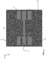
- FIG. 2 - FIG. 5 show a method 20 according to an embodiment of the invention. In particular, steps 21-25 of the method 20 are illustrated.
- the method 20 is suitable for processing a semiconductor device 90 (e.g., see FIG. 9 ), wherein the semiconductor device 90 comprises at least two gates 41 and 43 (e.g., see FIG. 4 or FIG. 9 ) separated by a spacing 4a (see FIG. 5 ).
- FIG. 2 shows a step 21 of the method 20.
- a template structure 1 is formed.
- the template structure 1 includes at least one sub-structure 2a that has a dimension less than a CD.
- the CD may be 50nm or less, or may even be 30nm or less.
- the particular template structure 1 shown in FIG. 2 is merely an example.
- This template structure 1 comprises two sub-structures 2a, which are in the order of 5-30nm.
- the exemplary template structure 1 comprises a second sub-structure 2b, which has a width of around 50nm.
- the exemplary template structure 1 further comprises a plurality of gaps 2c, which have each a gap width of 30nm.
- This exemplary template structure 1 is suitable to process a spin-qubit semiconductor device 90 as shown in FIG. 9 .
- other template structures 1 for processing other types of semiconductor devices can likewise be used to implement the method 20.
- the template structure 1 may also be referred to as a Go layer, which is formed prior to a gate layer 3 (see FIG. 3 ), which may be referred to as a Gi layer.
- the template structure 1 can be printed by a NTD resist, which makes electron beam lithography feasible for obtaining the particular shape of the template structure 1. That is, the template structure 1, in particular the sub-structures 2a, 2b and the gaps 2c, can be printed by an electron beam into the NTD resist, which may then be developed and etched, or the like, to obtain the desired template structure 1 shape.
- the template structure 1 may comprise amorphous silicon, and/or Si 3 N 4 , and/or a SOC/SOG layer stack, and/or a SiOC/APF layer stack.
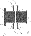
- FIG. 3 shows steps 22 and 23 of the method 20.
- a gate layer 3 e.g., the Gi layer
- the part of the gate layer 3 formed on the template structure 1 is removed.
- FIG. 3 shows the intermediate structure after step 23.
- the template structure 1 is exposed where the gate layer 3 is removed.
- the part of the gate layer 3 formed on the template structure 1 may be removed by CMP.
- FIG. 4 shows step 24 of the method 20.
- the remaining gate layer 3 i.e., after the removing step 23
- a gate structure comprising, for instance, the two gates 41 and 43 is formed.
- the substructure 2a of the template structure 1 is arranged between the gates 41 and 43.
- a gate 40 is formed, which has a width that corresponds to the width of the gap 2c in the template structure 1.
- gates 42 and 43 are formed and the substructure 2b of the template structure 1 is arranged between these gates 42 and 43.
- the gates 44 and 45 maybe like the gates 40 and 41.
- the patterning of the gate layer 3 may be carried out by lithography, in particular by optical lithography, i.e. using a light field.
- the patterning of the gate layer 3 does not involve patterning of CDs (all structures with CD or less are fabricated by the steps of method 20 using the template structure 1).
- the patterning of the gate layer 3 may be self-aligned on the template structure 1.
- the patterning of the gate layer 3 may comprise etching of the gate layer 3, wherein the gate layer etch may be selective to the material of the template structure 1, i.e. the template structure 1 may act as an etch stop for the gate layer etch, i.e., withstands the gate layer etch.
- FIG. 5 show step 25 of the method 20.
- the template structure 1 is selectively removed. It can be seen that removing the template structure 1 forms spacings in the gate layer 3. For instance, the spacing 4a is formed between the two gates 41 and 43 due to removing the sub-structure 2a. Further, the spacing 4b is formed between the gates 42 and 43 due to removing the sub-structure 2b.
- the method 20 enabled structuring gates with very small spacings, i.e. equal to or below the CD, in a simple manner and with high reliability.
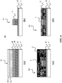
- FIG. 6 (a-d) and FIG. 7 (a-d) show a specific method according to an embodiment of the invention, which builds on the method 20 shown in FIG.2-FIG.5 .
- FIG. 6a shows a layer structure that may be used to form the template structure 1 by lithography.
- the layer structure comprises a substrate 7 (e.g., silicon), and oxide layer 8 (e.g., silicon oxide), a template layer 1a, 1b, and a NTD resist 6a, 6b.
- the template layer 1a, 1b may comprise amorphous silicon 1b covered by a hardmask layer 1a.
- the hardmask layer 1a may comprise a Si 3 N 4 layer, or a SOC/SOG layer stack, or a SiOC/APF layer stack.
- the NTD resist 6a, 6b may comprise a SOC layer 6a and a SOG layer 6b.
- the NTD resist 6a, 6b may coat the template layer 1a, 1b.
- the NTD resist 6a, 6b may then be patterned by electron beam printing and NTD. Notably, in case of such electron beam lithography, the SOC/SOG structure of the NTD resist is beneficial. If optical lithography or extreme ultraviolet lithography would be used instead, the NTD resist 6a, 6b may be formed by different, suitable layers.
- FIG. 6b shows the patterning of the template layer 1a, 1b into the template structure 1, i.e. corresponds to step 21.
- the patterning may comprise etching the template layer 1a, 1b using the patterned negative tone resist 6a, 6b as a mask to form the template structure 1.
- SOC/SOG may be etched first, followed by etching the hardmask layer 1a and the amorphous silicon 1b.
- a thickness of the hardmask layer 1a and amorphous silicon 1b may be selected to optimize the etching.
- the etching of the hardmask layer 1a and amorphous silicon maybe selected to the oxide layer 8, i.e., the oxide layer 8 may act as an etch stop.
- FIG. 6c shows the formation of the gate layer 3 on and around the template structure 1, i.e., corresponds to step 22.
- the gate layer 3 e.g., TiN
- the gate layer 3 is deposited to be thicker (higher in Fig. 6 ) as the template structure 1.
- FIG. 6d shows the removing of the part of the gate layer 3 formed on the template structure 1, which corresponds to step 23.
- CMP can be used on the gate layer 3 material (e.g., TiN).
- the hardmask layer 1a e.g. Si 3 N 4
- the template structure 1 surface is thereby exposed.
- the gate layer 3 and template structure 1 may form a common planar surface.
- FIG. 7a and 7b show patterning the gate layer 3 into a gate structure, thus corresponding to step 24.
- FIG. 7a shows a lithography of the gate layer 3.
- a resist comprising SOC and SOG may be coated onto the gate layer 3 and template structure 1, and patterned into an etch mask.
- FIG. 7b shows etching the gate layer 3 using the etch mask. Further, in order to preserve the template structure 1, the hardmask layer 1a of the template structure may not be affected by the gate layer 3 etch, and also the oxide layer 8 may serve as an etch stop.
- FIG. 7c shows removing the template structure 3, and thus corresponds to step 25.
- the spacings between the gate structure are formed, e.g., the spacings 4a and 4b shown in FIG. 4 .
- the template structure 1 may be selectively removed by wet etching using a hot phosphoric acid, or by selective dry etching.
- FIG. 7d shows finally the option to deposit a gate dielectric 10 (e.g., silicon oxide, in a range of 5-10nm) onto the gate structure.
- a gate dielectric 10 e.g., silicon oxide, in a range of 5-10nm
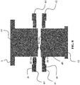
- FIG. 8 shows a resulting gate structure (structured gate layer 3) for specifically a semiconductor device 90, which is shown in FIG. 9 .
- the semiconductor device 90 is fabricated by using the method 20.
- the semiconductor device 90 of FIG. 9 comprises two SETs, which are coupled to a string of QDs.
- the gate structure of FIG. 8 shows that two gates 40 and 41 are formed for a first SET, and two gates 44 and 45 are formed for a second SET. Further, two confinement gates 42 and 43 are formed for defining the string of QDs.
- a spacing 4a between a gate 41 of a SET and a confinement gate 43 is in the range of 30nm or smaller (the same holds for the tip-to-tip distances of the other SET gates 40, 41, 44, 45 to the respective close confinement gate 42, 43). That is, the spacing 4a (formed by removing the sub-structure 2a) separates a gate 41 of the SET from a confinement gate 43. Further, a spacing 4b between the two confinement gates 42 and 43 is in the range of 50nm or smaller. That is, the two confinement gates 42 and 43 are separated the second spacing 4b (formed by removing the second sub-structure 2b). Further, a gate length 4c of the SET gate 40 (and each other SET gate 41, 44, 45) may be in the order of 30nm (defined by the width of the respective gate electrode, and initially bay the gap 2c).
- the method 20 provides several advantages for fabricating a semiconductor device 90.
- the method 20 enables a tunable tip-to-tip spacing from 5-50nm, particularly from 5-30nm. Further optimization is feasible to achieve below 5nm gaps.
- the method 20 reduces the charge noise in the semiconductor device 90 by reducing the number of gate layers (and by consequence gate dielectrics).
- the patterning of the gate layer 3 can be self-aligned on the template structure 1, leading to a simpler process.
- the patterning of the gate layer 3 into the gate structure can be simplified and less critical.
Landscapes
- Engineering & Computer Science (AREA)
- Manufacturing & Machinery (AREA)
- Electrodes Of Semiconductors (AREA)
- Thin Film Transistor (AREA)
Abstract
Description
- The present disclosure relates to semiconductor processing. In particular, the disclosure presents a method for processing a semiconductor device with two closely space gates, wherein closely spaced means below a critical dimension (CD), for instance, below 50nm or even 30nm. The method is particularly useful for processing a silicon spin-qubit based semiconductor device.
- With the ongoing miniaturization of semiconductor devices, also the distances between gates (i.e., the gate electrodes) become smaller and smaller. In particular, semiconductor devices that employ quantum effects, e.g., make use of quantum dots (QDs), quantum wires, or other low-dimensional structures, typically require gates that are separated from each other by not more than a CD. For instance, a CD from the tip of one gate to the tip of another gate (i.e., a tip-to-tip spacing) may have to be less than 50nm, or even less than 30nm for best device performance. Fabricating such semiconductor devices is very challenging, and new integrations schemes are thus required.
- For example, for the successful implementation of silicon spin-qubit based quantum computations, it is crucial to achieve high qubit readout signals. In this respect, a widely adopted approach is a semiconductor device using a single electron transistor (SET) to readout spin-qubits defined by a string of QDs. Thereby, the SET also serves as a qubit reservoir. In such an SET-based spin-qubit device, the spacing between a gate confining the QDs and a gate of the SET is a key design parameter. A smaller spacing leads to a significantly improved readout sensitivity. In particular, a spacing of less than 30nm would be desired between the SET gate and the confinement gate.
-
FIG. 1 shows in (a) a situation where two gates GA and GB of a semiconductor device are formed on the same gate layer and very close together, i.e., with a distance of at most 50nm. The gate material may exemplarily be TiN. - In a first exemplary method to fabricate such a semiconductor device, the small gate spacing could be achieved by overlapping multiple gate layers. However, the overlapping introduces extra gate dielectrics, which may negatively contribute to the device characteristics. For instance, the extra dielectrics may lead to charge noise, which is particularly detrimental for the above-mentioned spin-qubit based device. Therefore, the number of gate layers for such a device needs to be limited to less than three layers. In addition, this method involves a rather complex process.
- In a second exemplary method, a cut lithography is used. That is, the whole gate pattern, including the two gates GA and GB, is printed, e.g. by electron beam lithography, and is then cut/etched, in order to form the two separate gates GA and GB. However, the etch placement is thereby crucial, and aligning the etching tool with the previously printed gate pattern typically involves an overlay error of 8-15nm. Further, a positive tone development (PTD) resist is needed in this case for the electron beam lithography, making the implementation difficult, since electron beam lithography typically works much better with a negative tone development (NTD) resist. Another problem is that in the case of TiN being the gate material, the etching may lead to a tip shrinkage in the range of 15-20nm for each gate tip, which make it nearly impossible to achieve a spacing between the two gates of less than 50nm, or even of less than 30nm.
- In a third exemplary method, a spacer defined process is used. That is, a thick spacer is grown underneath one gate (e.g., below the gate of the SET in the above-mentioned spin-qubit device). However, a difficulty is then to pattern the two vertically displaced gates. In addition, it is difficult to remove the spacer.
- Therefore, a new method for fabricating such semiconductor devices with small gate (electrode) separation on the same gate layer, like the advanced silicon spin-qubit device, is needed.
- In particular, in view of the above-mentioned challenges and disadvantages of the conventional methods, embodiments of the present invention aim to provide an improved method for fabricating a semiconductor device with two gates placed closely together. An objective is to provide a reliable and not too complex method for forming the two gates on the same gate layer with a spacing below a CD, in particular, of less than 50nm, more particularly of less than 30nm.
- The objective is achieved by the embodiments of the invention provided in the enclosed independent claims. Advantageous implementations of these embodiments are defined in the dependent claims.
- In particular, embodiments of the invention address the challenge of the small gate spacing by using a "gate zero" (Go) layer that acts as a self-aligned mask for a "gate one" (Gi) layer. The CD of the Go layer can be in the range of 10-30 nm. Meanwhile, by extending the Go layer to a fanout region, the patterning of subsequent gate layers (e.g., the Gi layer) can be simplified and less critical.
- A first aspect of the present disclosure provides a method for processing a semiconductor device, wherein the semiconductor device comprises two gates separated by a spacing, and wherein the method comprises: forming a template structure, wherein the template structure includes at least one sub-structure having a dimension less than a critical dimension (CD) forming a gate layer on and around the template structure; removing the part of the gate layer formed on the template structure; patterning the remaining gate layer into a gate structure including the two gates; and selectively removing the template structure, wherein the spacing between the two gates is formed by the removed sub-structure.
- The method of the first aspect may form a very small spacing between the two gates, while avoiding the disadvantages of the exemplary methods mentioned above. The method is thereby reliable and comparatively simple.
- Notably, the template structure may be the "gate zero layer", and the gate layer may be the "gate one layer", as mentioned above.
- In an implementation of the method, the CD is 50nm or less, particularly is 40nm or less, more particularly is 30nm or less.
- That is, the method can form a spacing between the two gates of less than 40nm, or less than 40nm, or even less than 30nm. Thus, it maybe used in the fabrication of a SET gate close to a confinement gate in a spin-qubit device.
- In an implementation of the method, the template structure is formed by electron beam lithography, or optical lithography, or extreme ultraviolet lithography.
- This allows patterning the template structure, in particular the at least one sub-structure having one or more dimensions less than the CD, with high precision and reliability.
- In an implementation of the method, the electron beam lithography comprises printing the shape of the template structure into a negative tone resist by electron beam.
- The NTD resist allows the electron beam lithography to produce particularly small sub-structures, and overcomes the disadvantages of the exemplary methods using PTD resist
- In an implementation of the method, the template structure is formed by providing a template layer, coating the template layer with a negative tone resist, patterning the negative tone resist by electron beam printing and negative tone development, and etching the template layer using the patterned negative tone resist as a mask.
- In an implementation of the method, the negative tone resist comprises a spin on carbon (SOC) layer and/or a spin on glass (SOG) layer.
- In an implementation of the method, the template structure comprises amorphous silicon covered by a hardmask layer.
- In an implementation of the method, the hardmask layer comprises a Si3N4 layer, or a SOC/SOG layer stack, or a SiOC/Advanced Patterning Film (APF) layer stack.
- In an implementation of the method, the part of the gate layer formed on the template structure is removed by chemical mechanical polishing, CMP.
- In an implementation of the method, the hardmask layer serves as an etch stop for the CMP.
- Thus, the gate layer can be removed accurately from the template structure.
- In an implementation of the method, patterning the remaining gate layer into the gate structure comprises etching the gate layer, wherein the hardmask layer serves as an etch stop for the gate layer etching.
- Thus, the gate layer can be patterned accurately. Notably, patterning the gate layer is relaxed in comparison with the exemplary methods, since the spacings between the gates and other small gaps do not have to be patterned when using the method of the first aspect.
- In an implementation of the method, the gate layer comprises titanium nitride.
- In an implementation of the method, the template structure is removed by wet etching using a hot phosphoric acid, or is removed by selective dry etching.
- In an implementation of the method, the semiconductor device comprises a single electron transistor (SET) which is coupled to a string of quantum dots (QD); and the spacing separates a gate of the SET from a confinement gate defining the string ofQD.
- The spacing can be less than 30nm, thus improving significantly the spin-qubit readout.
- In an implementation of the method, the template structure comprises a second sub-structure, particularly having a dimension less than 50nm or less than the CD; the string of QD is formed between the confinement gate and a second confinement gate; the two confinement gates are separated by a second spacing; and the second spacing between the confinement gates is formed by the removed second sub-structure of the template structure.
- The second substructure can, in particular, be formed with a high aspect ratio between length and width. While the width may be less than 50nm, or even less than 30nm, the length can be much larger, allowing multiple qubits to be defined between the confinement gates. The width can be kept constant along the length of the sub-structure.
- In an implementation of the method, the template structure comprises a gap having a dimension less than the CD; the gate of the SET is formed by forming the gate layer in the gap and then removing the part of the gate layer formed on top of the template structure; and the dimension of the gap defines a length of the gate of the SET.
- The gate length can be made 50nm or less, or even 30nm or less.
- A second aspect of the present disclosure provides a semiconductor device fabricated by using the method according to the first aspect or any implementation forms thereof.
- The semiconductor device enjoys the advantages of the method of the first aspect. That is, it can have well defined spacings and gate length that are less than a CD, for instance, less than 50nm, or even less than 30nm.
- The above described aspects and implementations are explained in the following description of embodiments with respect to the enclosed drawings:
- FIG. 1
- shows two gates of a semiconductor device spaced close to each other.
- FIG. 2
- illustrates a steps of a method according to an embodiment of the invention.
- FIG. 3
- illustrates further steps of the method according to an embodiment of the invention.
- FIG. 4
- illustrates a further step of the method according to an embodiment of the invention.
- FIG. 5
- illustrates a further step of the method according to an embodiment of the invention.
- FIG. 6
- shows steps of a detailed method according to an embodiment of the invention.
- FIG. 7
- shows further steps of the detailed method according to an embodiment of the invention.
- FIG. 8
- illustrates critical structural features of gates of a semiconductor device according to an embodiment of the invention.
- FIG. 9
- shows a semiconductor device according to an embodiment of the invention.
-
FIG. 2 - FIG. 5 show amethod 20 according to an embodiment of the invention. In particular, steps 21-25 of themethod 20 are illustrated. Themethod 20 is suitable for processing a semiconductor device 90 (e.g., seeFIG. 9 ), wherein thesemiconductor device 90 comprises at least twogates 41 and 43 (e.g., seeFIG. 4 orFIG. 9 ) separated by aspacing 4a (seeFIG. 5 ). -
FIG. 2 shows astep 21 of themethod 20. In particular, in step 21 atemplate structure 1 is formed. Thetemplate structure 1 includes at least onesub-structure 2a that has a dimension less than a CD. For instance, the CD may be 50nm or less, or may even be 30nm or less. - The
particular template structure 1 shown inFIG. 2 is merely an example. Thistemplate structure 1 comprises twosub-structures 2a, which are in the order of 5-30nm. Further, theexemplary template structure 1 comprises asecond sub-structure 2b, which has a width of around 50nm. Theexemplary template structure 1 further comprises a plurality of gaps 2c, which have each a gap width of 30nm. Thisexemplary template structure 1 is suitable to process a spin-qubit semiconductor device 90 as shown inFIG. 9 . However,other template structures 1 for processing other types of semiconductor devices can likewise be used to implement themethod 20. - The
template structure 1 may also be referred to as a Go layer, which is formed prior to a gate layer 3 (seeFIG. 3 ), which may be referred to as a Gi layer. Thetemplate structure 1 can be printed by a NTD resist, which makes electron beam lithography feasible for obtaining the particular shape of thetemplate structure 1. That is, thetemplate structure 1, in particular the sub-structures 2a, 2b and the gaps 2c, can be printed by an electron beam into the NTD resist, which may then be developed and etched, or the like, to obtain the desiredtemplate structure 1 shape. - Structures of critical CD in the
gate layer 3 can be defined by thetemplate structure 1. Thetemplate structure 1 may comprise amorphous silicon, and/or Si3N4, and/or a SOC/SOG layer stack, and/or a SiOC/APF layer stack. -
FIG. 3 showssteps method 20. In particular, in step 22 a gate layer 3 (e.g., the Gi layer) is formed on and around thetemplate structure 1. Then, instep 23, the part of thegate layer 3 formed on thetemplate structure 1 is removed.FIG. 3 shows the intermediate structure afterstep 23. Thetemplate structure 1 is exposed where thegate layer 3 is removed. The part of thegate layer 3 formed on thetemplate structure 1 may be removed by CMP. -
FIG. 4 shows step 24 of themethod 20. Instep 24, the remaining gate layer 3 (i.e., after the removing step 23) is patterned into a gate structure including the at least two gates (i.e., gate electrodes), here exemplarily the gates 41-45. InFIG. 4 , a gate structure comprising, for instance, the twogates substructure 2a of thetemplate structure 1 is arranged between thegates gate 40 is formed, which has a width that corresponds to the width of the gap 2c in thetemplate structure 1. Further,gates substructure 2b of thetemplate structure 1 is arranged between thesegates gates gates - The patterning of the
gate layer 3 may be carried out by lithography, in particular by optical lithography, i.e. using a light field. The patterning of thegate layer 3 does not involve patterning of CDs (all structures with CD or less are fabricated by the steps ofmethod 20 using the template structure 1). The patterning of thegate layer 3 may be self-aligned on thetemplate structure 1. The patterning of thegate layer 3 may comprise etching of thegate layer 3, wherein the gate layer etch may be selective to the material of thetemplate structure 1, i.e. thetemplate structure 1 may act as an etch stop for the gate layer etch, i.e., withstands the gate layer etch. -
FIG. 5 show step 25 of themethod 20. In particular, instep 25 thetemplate structure 1 is selectively removed. It can be seen that removing thetemplate structure 1 forms spacings in thegate layer 3. For instance, thespacing 4a is formed between the twogates sub-structure 2a. Further, thespacing 4b is formed between thegates sub-structure 2b. Thus, themethod 20 enabled structuring gates with very small spacings, i.e. equal to or below the CD, in a simple manner and with high reliability. -
FIG. 6 (a-d) andFIG. 7 (a-d) show a specific method according to an embodiment of the invention, which builds on themethod 20 shown inFIG.2-FIG.5 . -
FIG. 6a shows a layer structure that may be used to form thetemplate structure 1 by lithography. In particular, the layer structure comprises a substrate 7 (e.g., silicon), and oxide layer 8 (e.g., silicon oxide), atemplate layer 1a, 1b, and a NTD resist 6a, 6b. Thetemplate layer 1a, 1b may comprise amorphous silicon 1b covered by ahardmask layer 1a. Thehardmask layer 1a may comprise a Si3N4 layer, or a SOC/SOG layer stack, or a SiOC/APF layer stack. The NTD resist 6a, 6b may comprise a SOC layer 6a and aSOG layer 6b. The NTD resist 6a, 6b may coat thetemplate layer 1a, 1b. - The NTD resist 6a, 6b may then be patterned by electron beam printing and NTD. Notably, in case of such electron beam lithography, the SOC/SOG structure of the NTD resist is beneficial. If optical lithography or extreme ultraviolet lithography would be used instead, the NTD resist 6a, 6b may be formed by different, suitable layers.
-
FIG. 6b then shows the patterning of thetemplate layer 1a, 1b into thetemplate structure 1, i.e. corresponds to step 21. In particular, the patterning may comprise etching thetemplate layer 1a, 1b using the patterned negative tone resist 6a, 6b as a mask to form thetemplate structure 1. For instance, SOC/SOG may be etched first, followed by etching thehardmask layer 1a and the amorphous silicon 1b. A thickness of thehardmask layer 1a and amorphous silicon 1b may be selected to optimize the etching. The etching of thehardmask layer 1a and amorphous silicon maybe selected to theoxide layer 8, i.e., theoxide layer 8 may act as an etch stop. -
FIG. 6c shows the formation of thegate layer 3 on and around thetemplate structure 1, i.e., corresponds to step 22. In particular, the gate layer 3 (e.g., TiN) may be deposited onto and surrounding thetemplate structure 1. Thegate layer 3 is deposited to be thicker (higher inFig. 6 ) as thetemplate structure 1. -
FIG. 6d then shows the removing of the part of thegate layer 3 formed on thetemplate structure 1, which corresponds to step 23. To this end, CMP can be used on thegate layer 3 material (e.g., TiN). Thehardmask layer 1a (e.g. Si3N4) may thereby serve as an etch stop for the CMP. Thetemplate structure 1 surface is thereby exposed. Thegate layer 3 andtemplate structure 1 may form a common planar surface. -
FIG. 7a and 7b show patterning thegate layer 3 into a gate structure, thus corresponding to step 24. In particular,FIG. 7a shows a lithography of thegate layer 3. To this end, a resist comprising SOC and SOG may be coated onto thegate layer 3 andtemplate structure 1, and patterned into an etch mask. -
FIG. 7b shows etching thegate layer 3 using the etch mask. Further, in order to preserve thetemplate structure 1, thehardmask layer 1a of the template structure may not be affected by thegate layer 3 etch, and also theoxide layer 8 may serve as an etch stop. -
FIG. 7c shows removing thetemplate structure 3, and thus corresponds to step 25. By removing thetemplate structure 1, the spacings between the gate structure are formed, e.g., thespacings FIG. 4 . Thetemplate structure 1 may be selectively removed by wet etching using a hot phosphoric acid, or by selective dry etching. -
FIG. 7d shows finally the option to deposit a gate dielectric 10 (e.g., silicon oxide, in a range of 5-10nm) onto the gate structure.
5 nm SiO2 deposition -
FIG. 8 shows a resulting gate structure (structured gate layer 3) for specifically asemiconductor device 90, which is shown inFIG. 9 . Thesemiconductor device 90 is fabricated by using themethod 20. Thesemiconductor device 90 ofFIG. 9 comprises two SETs, which are coupled to a string of QDs. The gate structure ofFIG. 8 shows that twogates gates confinement gates - A
spacing 4a between agate 41 of a SET and aconfinement gate 43 is in the range of 30nm or smaller (the same holds for the tip-to-tip distances of theother SET gates close confinement gate 42, 43). That is, thespacing 4a (formed by removing the sub-structure 2a) separates agate 41 of the SET from aconfinement gate 43. Further, aspacing 4b between the twoconfinement gates confinement gates second spacing 4b (formed by removing thesecond sub-structure 2b). Further, agate length 4c of the SET gate 40 (and eachother SET gate - In summary, the
method 20 provides several advantages for fabricating asemiconductor device 90. In particular, themethod 20 enables a tunable tip-to-tip spacing from 5-50nm, particularly from 5-30nm. Further optimization is feasible to achieve below 5nm gaps. In addition, themethod 20 reduces the charge noise in thesemiconductor device 90 by reducing the number of gate layers (and by consequence gate dielectrics). Further, the patterning of thegate layer 3 can be self-aligned on thetemplate structure 1, leading to a simpler process. Furthermore, the patterning of thegate layer 3 into the gate structure can be simplified and less critical. - The present disclosure has been described in conjunction with embodiments and examples as well as aspects and implementations. However, other variations can be understood and effected by persons skilled in the art from the studies of the drawings, the description and the claims. In the claims as well as in the description the word "comprising" does not exclude other elements or steps and the indefinite article "a" or "an" does not exclude a plurality.
Claims (17)
- A method (20) for processing a semiconductor device (90), wherein the semiconductor device (90) comprises two gates (41, 43) separated by a spacing (4a), and wherein the method (20) comprises:forming (21) a template structure (1), wherein the template structure (1) includes at least one sub-structure (2a) having a dimension less than a critical dimension, CD;forming (22) a gate layer (3) on and around the template structure (1);removing (23) the part of the gate layer (3) formed on the template structure (1);patterning (24) the remaining gate layer (3) into a gate structure including the two gates (41, 43); andselectively removing (25) the template structure (1), wherein the spacing (4a) between the two gates (41, 43) is formed by the removed sub-structure (2a).
- The method (20) according to claim 1, wherein:
the CD is 50nm or less, particularly is 40nm or less, more particularly is 30nm or less. - The method (20) according to claim 1 or 2, wherein:
the template structure (1) is formed by electron beam lithography, or optical lithography, or extreme ultraviolet lithography. - The method (20) according to claim 3, wherein:
the electron beam lithography comprises printing the shape of the template structure (1) into a negative tone resist by electron beam. - The method (20) according to claim 3 or 4, wherein:
the template structure (1) is formed by providing a template layer (1a, 1b), coating the template layer (1a, 1b) with a negative tone resist (6a, 6b), patterning the negative tone resist (6a, 6b) by electron beam printing and negative tone development, and etching the template layer (1a, 1b) using the patterned negative tone resist (6a, 6b) as a mask. - The method (20) according to claim 4 or 5, wherein:
the negative tone resist (6a, 6b) comprises a spin on carbon, SOC, layer (6a) and/or a spin on glass, SOG, layer (6b). - The method (20) according to one of the claims 1 to 6, wherein:
the template structure (1) comprises amorphous silicon (1b) covered by a hardmask layer (1a). - The method (20) according to claim 7, wherein:
the hardmask layer (1a) comprises a Si3N4 layer, or a SOC/SOG layer stack, or a SiOC/Advanced Patterning Film, APF, layer stack. - The method (20) according to one of the claims 1 to 8, wherein:
the part of the gate layer (3) formed on the template structure (1) is removed by chemical mechanical polishing, CMP. - The method (20) according to the claims 8 and 9, wherein:
the hardmask layer (1a) serves as an etch stop for the CMP. - The method (20) according to the claims 8 and 9 or according to claim 10, wherein:
patterning (24) the remaining gate layer (3) into the gate structure comprises etching the gate layer (3), wherein the hardmask layer (1a) serves as an etch stop for the gate layer etching. - The method (20) according to one of the claims 1 to 11, wherein:
the gate layer (3) comprises titanium nitride. - The method (20) according to one of the claims 1 to 12, wherein:
the template structure (1) is removed by wet etching using a hot phosphoric acid, or is removed by selective dry etching. - The method (20) according to one of the claims 1 to 13, wherein:the semiconductor device (90) comprises a single electron transistor, SET, which is coupled to a string of quantum dots, QD; andthe spacing (4a) separates a gate (41) of the SET from a confinement gate (43) defining the string of QD.
- The method (20) according to claim 14, wherein:the template structure (1) comprises a second sub-structure (2b), particularly having a dimension less than 50nm or less than the CD;the string of QD is formed between the confinement gate (31) and a second confinement gate (42);the two confinement gates (42, 43) are separated by a second spacing (4b); andthe second spacing (4b) between the confinement gates (42, 43) is formed by the removed second sub-structure (2b) of the template structure (1).
- The method (20) according to claim 14 or 15, wherein:the template structure (1) comprises a gap (2c) having a dimension less than the CD;the gate (41) of the SET is formed by forming the gate layer (3) in the gap (2c) and then removing the part of the gate layer (3) formed on top of the template structure (1); andthe dimension of the gap (2c) defines a length (4c) of the gate (41) of the SET.
- Semiconductor device (90) fabricated by using the method (20) according to any one of the claims 1 to 16.
Priority Applications (3)
| Application Number | Priority Date | Filing Date | Title |
|---|---|---|---|
| EP20179631.5A EP3922596A1 (en) | 2020-06-12 | 2020-06-12 | A method for processing a semiconductor device with two closely spaced gates |
| US17/345,827 US11638391B2 (en) | 2020-06-12 | 2021-06-11 | Method for processing a semiconductor device with two closely spaced gates |
| CN202110659926.1A CN113809164A (en) | 2020-06-12 | 2021-06-11 | Method for processing a semiconductor device having two closely spaced gates |
Applications Claiming Priority (1)
| Application Number | Priority Date | Filing Date | Title |
|---|---|---|---|
| EP20179631.5A EP3922596A1 (en) | 2020-06-12 | 2020-06-12 | A method for processing a semiconductor device with two closely spaced gates |
Publications (1)
| Publication Number | Publication Date |
|---|---|
| EP3922596A1 true EP3922596A1 (en) | 2021-12-15 |
Family
ID=71096501
Family Applications (1)
| Application Number | Title | Priority Date | Filing Date |
|---|---|---|---|
| EP20179631.5A Pending EP3922596A1 (en) | 2020-06-12 | 2020-06-12 | A method for processing a semiconductor device with two closely spaced gates |
Country Status (3)
| Country | Link |
|---|---|
| US (1) | US11638391B2 (en) |
| EP (1) | EP3922596A1 (en) |
| CN (1) | CN113809164A (en) |
Citations (7)
| Publication number | Priority date | Publication date | Assignee | Title |
|---|---|---|---|---|
| US20140193980A1 (en) * | 2013-01-04 | 2014-07-10 | Taiwan Semicondutor Manufacturing Compnay Limited | Patterned line end space |
| US20150279981A1 (en) * | 2013-03-14 | 2015-10-01 | Wisconsin Alumni Research Foundation | Direct tunnel barrier control gates in a two-dimensional electronic system |
| US20190044048A1 (en) * | 2018-02-08 | 2019-02-07 | Intel Corporation | Sidewall metal spacers for forming metal gates in quantum devices |
| US20190044049A1 (en) * | 2018-02-20 | 2019-02-07 | Intel Corporation | Gate arrangements in quantum dot devices |
| US20190198618A1 (en) * | 2016-09-30 | 2019-06-27 | Intel Corporation | Quantum dot devices with single electron transistor detectors |
| US20190229189A1 (en) * | 2016-08-10 | 2019-07-25 | Intel Corporation | Quantum dot array devices |
| US20200066629A1 (en) * | 2016-12-23 | 2020-02-27 | Intel Corporation | Advanced lithography and self-assembled devices |
Family Cites Families (6)
| Publication number | Priority date | Publication date | Assignee | Title |
|---|---|---|---|---|
| DE10230696B4 (en) * | 2002-07-08 | 2005-09-22 | Infineon Technologies Ag | Method for producing a short channel field effect transistor |
| DE102005051972B4 (en) * | 2005-10-31 | 2012-05-31 | Infineon Technologies Ag | Combined electron beam and optical lithography process |
| EP3082073B1 (en) | 2015-04-12 | 2019-01-16 | Hitachi Ltd. | Quantum information processing |
| US9934985B2 (en) * | 2015-11-30 | 2018-04-03 | Taiwan Semiconductor Manufacturing Company, Ltd. | Critical dimension control for double patterning process |
| US20190067115A1 (en) * | 2017-08-23 | 2019-02-28 | Globalfoundries Inc. | Gate cut method for replacement metal gate |
| EP3480842A1 (en) * | 2017-11-02 | 2019-05-08 | IMEC vzw | Method for forming source/drain contacts |
-
2020
- 2020-06-12 EP EP20179631.5A patent/EP3922596A1/en active Pending
-
2021
- 2021-06-11 CN CN202110659926.1A patent/CN113809164A/en active Pending
- 2021-06-11 US US17/345,827 patent/US11638391B2/en active Active
Patent Citations (7)
| Publication number | Priority date | Publication date | Assignee | Title |
|---|---|---|---|---|
| US20140193980A1 (en) * | 2013-01-04 | 2014-07-10 | Taiwan Semicondutor Manufacturing Compnay Limited | Patterned line end space |
| US20150279981A1 (en) * | 2013-03-14 | 2015-10-01 | Wisconsin Alumni Research Foundation | Direct tunnel barrier control gates in a two-dimensional electronic system |
| US20190229189A1 (en) * | 2016-08-10 | 2019-07-25 | Intel Corporation | Quantum dot array devices |
| US20190198618A1 (en) * | 2016-09-30 | 2019-06-27 | Intel Corporation | Quantum dot devices with single electron transistor detectors |
| US20200066629A1 (en) * | 2016-12-23 | 2020-02-27 | Intel Corporation | Advanced lithography and self-assembled devices |
| US20190044048A1 (en) * | 2018-02-08 | 2019-02-07 | Intel Corporation | Sidewall metal spacers for forming metal gates in quantum devices |
| US20190044049A1 (en) * | 2018-02-20 | 2019-02-07 | Intel Corporation | Gate arrangements in quantum dot devices |
Also Published As
| Publication number | Publication date |
|---|---|
| US20210391526A1 (en) | 2021-12-16 |
| CN113809164A (en) | 2021-12-17 |
| US11638391B2 (en) | 2023-04-25 |
Similar Documents
| Publication | Publication Date | Title |
|---|---|---|
| US20090047788A1 (en) | Method for fabricating semiconductor device | |
| CN102592967B (en) | Semiconductor component and manufacturing method thereof | |
| US9214356B2 (en) | Mechanisms for forming patterns | |
| JP2009158907A (en) | Method for forming fine pattern of semiconductor element | |
| CN101364533B (en) | method of patterning | |
| CN110544671A (en) | Method for forming semiconductor structure | |
| TWI637233B (en) | Variable space mandrel cut for self aligned double pattering and method of manufacturing the same | |
| US11769691B2 (en) | Semiconductor device and formation method thereof | |
| US20090170310A1 (en) | Method of forming a metal line of a semiconductor device | |
| US11183395B2 (en) | Semiconductor device and fabrication method thereof | |
| CN113192958B (en) | Memory device and method of manufacturing the same | |
| US11638391B2 (en) | Method for processing a semiconductor device with two closely spaced gates | |
| US12443100B2 (en) | Mask pattern | |
| CN117080054B (en) | Method for preparing semiconductor structure | |
| US11594423B2 (en) | Forming method of capacitor array and semiconductor structure | |
| CN115662944A (en) | Method for manufacturing semiconductor structure | |
| US11049721B2 (en) | Method and process for forming memory hole patterns | |
| US20210320007A1 (en) | Semiconductor structure and fabrication method thereof | |
| EP4372787A1 (en) | A method for producing a pattern of closely spaced features | |
| CN113496877A (en) | Method for forming semiconductor structure | |
| KR100526480B1 (en) | Method for fabricating non-volatile memory using quantum dot | |
| US20240170559A1 (en) | Method for producing closely spaced gate structures of a quantum dot device | |
| US20090256221A1 (en) | Method for making very small isolated dots on substrates | |
| JP2010117396A (en) | Method of preparing spot size conversion element | |
| KR100744242B1 (en) | Patterning method using scanning probe microscope |
Legal Events
| Date | Code | Title | Description |
|---|---|---|---|
| PUAI | Public reference made under article 153(3) epc to a published international application that has entered the european phase |
Free format text: ORIGINAL CODE: 0009012 |
|
| STAA | Information on the status of an ep patent application or granted ep patent |
Free format text: STATUS: THE APPLICATION HAS BEEN PUBLISHED |
|
| AK | Designated contracting states |
Kind code of ref document: A1 Designated state(s): AL AT BE BG CH CY CZ DE DK EE ES FI FR GB GR HR HU IE IS IT LI LT LU LV MC MK MT NL NO PL PT RO RS SE SI SK SM TR |
|
| B565 | Issuance of search results under rule 164(2) epc |
Effective date: 20201207 |
|
| STAA | Information on the status of an ep patent application or granted ep patent |
Free format text: STATUS: REQUEST FOR EXAMINATION WAS MADE |
|
| 17P | Request for examination filed |
Effective date: 20220527 |
|
| RBV | Designated contracting states (corrected) |
Designated state(s): AL AT BE BG CH CY CZ DE DK EE ES FI FR GB GR HR HU IE IS IT LI LT LU LV MC MK MT NL NO PL PT RO RS SE SI SK SM TR |