EP3920673A1 - Flexible harness assembly for surface mounted devices - Google Patents
Flexible harness assembly for surface mounted devices Download PDFInfo
- Publication number
- EP3920673A1 EP3920673A1 EP21169476.5A EP21169476A EP3920673A1 EP 3920673 A1 EP3920673 A1 EP 3920673A1 EP 21169476 A EP21169476 A EP 21169476A EP 3920673 A1 EP3920673 A1 EP 3920673A1
- Authority
- EP
- European Patent Office
- Prior art keywords
- trace
- harness assembly
- substrate
- vias
- fingers
- Prior art date
- Legal status (The legal status is an assumption and is not a legal conclusion. Google has not performed a legal analysis and makes no representation as to the accuracy of the status listed.)
- Pending
Links
Images



Classifications
-
- H—ELECTRICITY
- H05—ELECTRIC TECHNIQUES NOT OTHERWISE PROVIDED FOR
- H05K—PRINTED CIRCUITS; CASINGS OR CONSTRUCTIONAL DETAILS OF ELECTRIC APPARATUS; MANUFACTURE OF ASSEMBLAGES OF ELECTRICAL COMPONENTS
- H05K1/00—Printed circuits
- H05K1/02—Details
- H05K1/11—Printed elements for providing electric connections to or between printed circuits
- H05K1/115—Via connections; Lands around holes or via connections
-
- H—ELECTRICITY
- H05—ELECTRIC TECHNIQUES NOT OTHERWISE PROVIDED FOR
- H05K—PRINTED CIRCUITS; CASINGS OR CONSTRUCTIONAL DETAILS OF ELECTRIC APPARATUS; MANUFACTURE OF ASSEMBLAGES OF ELECTRICAL COMPONENTS
- H05K1/00—Printed circuits
- H05K1/02—Details
- H05K1/11—Printed elements for providing electric connections to or between printed circuits
-
- H—ELECTRICITY
- H05—ELECTRIC TECHNIQUES NOT OTHERWISE PROVIDED FOR
- H05K—PRINTED CIRCUITS; CASINGS OR CONSTRUCTIONAL DETAILS OF ELECTRIC APPARATUS; MANUFACTURE OF ASSEMBLAGES OF ELECTRICAL COMPONENTS
- H05K1/00—Printed circuits
- H05K1/18—Printed circuits structurally associated with non-printed electric components
- H05K1/182—Printed circuits structurally associated with non-printed electric components associated with components mounted in printed circuit boards [PCB], e.g. insert-mounted components [IMC]
- H05K1/183—Printed circuits structurally associated with non-printed electric components associated with components mounted in printed circuit boards [PCB], e.g. insert-mounted components [IMC] associated with components mounted in and supported by recessed areas of the PCBs
-
- H—ELECTRICITY
- H01—ELECTRIC ELEMENTS
- H01R—ELECTRICALLY-CONDUCTIVE CONNECTIONS; STRUCTURAL ASSOCIATIONS OF A PLURALITY OF MUTUALLY-INSULATED ELECTRICAL CONNECTING ELEMENTS; COUPLING DEVICES; CURRENT COLLECTORS
- H01R12/00—Structural associations of a plurality of mutually-insulated electrical connecting elements, specially adapted for printed circuits, e.g. printed circuit boards [PCB], flat or ribbon cables, or like generally planar structures, e.g. terminal strips, terminal blocks; Coupling devices specially adapted for printed circuits, flat or ribbon cables, or like generally planar structures; Terminals specially adapted for contact with, or insertion into, printed circuits, flat or ribbon cables, or like generally planar structures
- H01R12/50—Fixed connections
- H01R12/51—Fixed connections for rigid printed circuits or like structures
- H01R12/55—Fixed connections for rigid printed circuits or like structures characterised by the terminals
- H01R12/57—Fixed connections for rigid printed circuits or like structures characterised by the terminals surface mounting terminals
-
- H—ELECTRICITY
- H01—ELECTRIC ELEMENTS
- H01B—CABLES; CONDUCTORS; INSULATORS; SELECTION OF MATERIALS FOR THEIR CONDUCTIVE, INSULATING OR DIELECTRIC PROPERTIES
- H01B13/00—Apparatus or processes specially adapted for manufacturing conductors or cables
- H01B13/012—Apparatus or processes specially adapted for manufacturing conductors or cables for manufacturing wire harnesses
-
- H—ELECTRICITY
- H01—ELECTRIC ELEMENTS
- H01B—CABLES; CONDUCTORS; INSULATORS; SELECTION OF MATERIALS FOR THEIR CONDUCTIVE, INSULATING OR DIELECTRIC PROPERTIES
- H01B7/00—Insulated conductors or cables characterised by their form
-
- H—ELECTRICITY
- H01—ELECTRIC ELEMENTS
- H01B—CABLES; CONDUCTORS; INSULATORS; SELECTION OF MATERIALS FOR THEIR CONDUCTIVE, INSULATING OR DIELECTRIC PROPERTIES
- H01B7/00—Insulated conductors or cables characterised by their form
- H01B7/0045—Cable-harnesses
-
- H—ELECTRICITY
- H05—ELECTRIC TECHNIQUES NOT OTHERWISE PROVIDED FOR
- H05K—PRINTED CIRCUITS; CASINGS OR CONSTRUCTIONAL DETAILS OF ELECTRIC APPARATUS; MANUFACTURE OF ASSEMBLAGES OF ELECTRICAL COMPONENTS
- H05K1/00—Printed circuits
- H05K1/02—Details
- H05K1/0213—Electrical arrangements not otherwise provided for
- H05K1/0216—Reduction of cross-talk, noise or electromagnetic interference
-
- H—ELECTRICITY
- H05—ELECTRIC TECHNIQUES NOT OTHERWISE PROVIDED FOR
- H05K—PRINTED CIRCUITS; CASINGS OR CONSTRUCTIONAL DETAILS OF ELECTRIC APPARATUS; MANUFACTURE OF ASSEMBLAGES OF ELECTRICAL COMPONENTS
- H05K1/00—Printed circuits
- H05K1/02—Details
- H05K1/0277—Bendability or stretchability details
- H05K1/028—Bending or folding regions of flexible printed circuits
-
- H—ELECTRICITY
- H05—ELECTRIC TECHNIQUES NOT OTHERWISE PROVIDED FOR
- H05K—PRINTED CIRCUITS; CASINGS OR CONSTRUCTIONAL DETAILS OF ELECTRIC APPARATUS; MANUFACTURE OF ASSEMBLAGES OF ELECTRICAL COMPONENTS
- H05K1/00—Printed circuits
- H05K1/02—Details
- H05K1/0296—Conductive pattern lay-out details not covered by sub groups H05K1/02 - H05K1/0295
-
- H—ELECTRICITY
- H05—ELECTRIC TECHNIQUES NOT OTHERWISE PROVIDED FOR
- H05K—PRINTED CIRCUITS; CASINGS OR CONSTRUCTIONAL DETAILS OF ELECTRIC APPARATUS; MANUFACTURE OF ASSEMBLAGES OF ELECTRICAL COMPONENTS
- H05K1/00—Printed circuits
- H05K1/02—Details
- H05K1/09—Use of materials for the conductive, e.g. metallic pattern
-
- H—ELECTRICITY
- H05—ELECTRIC TECHNIQUES NOT OTHERWISE PROVIDED FOR
- H05K—PRINTED CIRCUITS; CASINGS OR CONSTRUCTIONAL DETAILS OF ELECTRIC APPARATUS; MANUFACTURE OF ASSEMBLAGES OF ELECTRICAL COMPONENTS
- H05K1/00—Printed circuits
- H05K1/02—Details
- H05K1/11—Printed elements for providing electric connections to or between printed circuits
- H05K1/115—Via connections; Lands around holes or via connections
- H05K1/116—Lands, clearance holes or other lay-out details concerning the surrounding of a via
-
- H—ELECTRICITY
- H05—ELECTRIC TECHNIQUES NOT OTHERWISE PROVIDED FOR
- H05K—PRINTED CIRCUITS; CASINGS OR CONSTRUCTIONAL DETAILS OF ELECTRIC APPARATUS; MANUFACTURE OF ASSEMBLAGES OF ELECTRICAL COMPONENTS
- H05K1/00—Printed circuits
- H05K1/02—Details
- H05K1/14—Structural association of two or more printed circuits
- H05K1/145—Arrangements wherein electric components are disposed between and simultaneously connected to two planar printed circuit boards, e.g. Cordwood modules
-
- H—ELECTRICITY
- H05—ELECTRIC TECHNIQUES NOT OTHERWISE PROVIDED FOR
- H05K—PRINTED CIRCUITS; CASINGS OR CONSTRUCTIONAL DETAILS OF ELECTRIC APPARATUS; MANUFACTURE OF ASSEMBLAGES OF ELECTRICAL COMPONENTS
- H05K1/00—Printed circuits
- H05K1/18—Printed circuits structurally associated with non-printed electric components
- H05K1/181—Printed circuits structurally associated with non-printed electric components associated with surface mounted components
-
- H—ELECTRICITY
- H05—ELECTRIC TECHNIQUES NOT OTHERWISE PROVIDED FOR
- H05K—PRINTED CIRCUITS; CASINGS OR CONSTRUCTIONAL DETAILS OF ELECTRIC APPARATUS; MANUFACTURE OF ASSEMBLAGES OF ELECTRICAL COMPONENTS
- H05K1/00—Printed circuits
- H05K1/18—Printed circuits structurally associated with non-printed electric components
- H05K1/189—Printed circuits structurally associated with non-printed electric components characterised by the use of flexible or folded printed circuits
-
- H—ELECTRICITY
- H05—ELECTRIC TECHNIQUES NOT OTHERWISE PROVIDED FOR
- H05K—PRINTED CIRCUITS; CASINGS OR CONSTRUCTIONAL DETAILS OF ELECTRIC APPARATUS; MANUFACTURE OF ASSEMBLAGES OF ELECTRICAL COMPONENTS
- H05K3/00—Apparatus or processes for manufacturing printed circuits
- H05K3/10—Apparatus or processes for manufacturing printed circuits in which conductive material is applied to the insulating support in such a manner as to form the desired conductive pattern
-
- H—ELECTRICITY
- H05—ELECTRIC TECHNIQUES NOT OTHERWISE PROVIDED FOR
- H05K—PRINTED CIRCUITS; CASINGS OR CONSTRUCTIONAL DETAILS OF ELECTRIC APPARATUS; MANUFACTURE OF ASSEMBLAGES OF ELECTRICAL COMPONENTS
- H05K3/00—Apparatus or processes for manufacturing printed circuits
- H05K3/22—Secondary treatment of printed circuits
-
- H—ELECTRICITY
- H05—ELECTRIC TECHNIQUES NOT OTHERWISE PROVIDED FOR
- H05K—PRINTED CIRCUITS; CASINGS OR CONSTRUCTIONAL DETAILS OF ELECTRIC APPARATUS; MANUFACTURE OF ASSEMBLAGES OF ELECTRICAL COMPONENTS
- H05K3/00—Apparatus or processes for manufacturing printed circuits
- H05K3/30—Assembling printed circuits with electric components, e.g. with resistors
- H05K3/303—Assembling printed circuits with electric components, e.g. with resistors with surface mounted components
-
- H—ELECTRICITY
- H05—ELECTRIC TECHNIQUES NOT OTHERWISE PROVIDED FOR
- H05K—PRINTED CIRCUITS; CASINGS OR CONSTRUCTIONAL DETAILS OF ELECTRIC APPARATUS; MANUFACTURE OF ASSEMBLAGES OF ELECTRICAL COMPONENTS
- H05K2201/00—Indexing scheme relating to printed circuits covered by H05K1/00
- H05K2201/09—Shape and layout
- H05K2201/09009—Substrate related
- H05K2201/09036—Recesses or grooves in insulating substrate
-
- H—ELECTRICITY
- H05—ELECTRIC TECHNIQUES NOT OTHERWISE PROVIDED FOR
- H05K—PRINTED CIRCUITS; CASINGS OR CONSTRUCTIONAL DETAILS OF ELECTRIC APPARATUS; MANUFACTURE OF ASSEMBLAGES OF ELECTRICAL COMPONENTS
- H05K2201/00—Indexing scheme relating to printed circuits covered by H05K1/00
- H05K2201/09—Shape and layout
- H05K2201/09209—Shape and layout details of conductors
- H05K2201/09218—Conductive traces
- H05K2201/09281—Layout details of a single conductor
-
- H—ELECTRICITY
- H05—ELECTRIC TECHNIQUES NOT OTHERWISE PROVIDED FOR
- H05K—PRINTED CIRCUITS; CASINGS OR CONSTRUCTIONAL DETAILS OF ELECTRIC APPARATUS; MANUFACTURE OF ASSEMBLAGES OF ELECTRICAL COMPONENTS
- H05K2201/00—Indexing scheme relating to printed circuits covered by H05K1/00
- H05K2201/10—Details of components or other objects attached to or integrated in a printed circuit board
- H05K2201/10007—Types of components
- H05K2201/10053—Switch
-
- H—ELECTRICITY
- H05—ELECTRIC TECHNIQUES NOT OTHERWISE PROVIDED FOR
- H05K—PRINTED CIRCUITS; CASINGS OR CONSTRUCTIONAL DETAILS OF ELECTRIC APPARATUS; MANUFACTURE OF ASSEMBLAGES OF ELECTRICAL COMPONENTS
- H05K2201/00—Indexing scheme relating to printed circuits covered by H05K1/00
- H05K2201/10—Details of components or other objects attached to or integrated in a printed circuit board
- H05K2201/10007—Types of components
- H05K2201/10151—Sensor
Definitions
- the disclosure relates generally to surface mounted devices (SMDs), and more particularly, to a flexible harness assembly for SMDs.
- SMDs surface mounted devices
- SMDs Surface mounted devices
- sensors such as negative/positive temperature coefficient sensors, reed switches, Anisotropic Magneto-Resistance (AMR) Giant Magneto-Resistance (GMR) sensors, Tunnel Magneto-Resistance (TMR) sensors, and/or fuses, or their combination, require connection to a control circuit.
- AMR Anisotropic Magneto-Resistance
- GMR Giant Magneto-Resistance
- TMR Tunnel Magneto-Resistance
- fuses or their combination
- One conventional assembly approach includes placing sensors on a printed circuit board (PCB) and connecting the sensors by wires afterwards.
- PCB printed circuit board
- wire harnesses are also employed to carry out the connection.
- wire harnessing can be expensive. Therefore, how to wire one or more devices, such as SMDs or sensors, without the use of conventional wire harnesses, is a critical problem to be addressed.
- a harness assembly may include a substrate having a plurality of vias, and a trace formed atop the substrate, the trace extending between each of the plurality of vias.
- the harness assembly may further include a surface mounted device disposed within a via of the plurality of vias.
- an assembly may include a substrate having a plurality of vias, and a trace formed atop the substrate, the trace extending between each of the plurality of vias.
- the assembly may further include a surface mounted device disposed within a via of the plurality of vias, the surface mounted device electrically connected with the trace.
- a method for forming a harness assembly may include providing a plurality of vias through a substrate, and forming a trace atop the substrate, the trace extending between each of the plurality of vias. The method may further include positioning a surface mounted device within a via of the plurality of vias.
- Embodiments herein provide an economical solution for low current carrying applications using a trace line connection to a flexible electronically conducting line deposited on a substrate.
- the substrate which may be flexible, has preset tabs or vias where SMD, such as sensors or fuses, can be attached.
- SMD such as sensors or fuses
- the advantage of this design is that long lead wires, sometimes required for the sensors, can be easily attached either manually or by automated line in a reflow furnace.
- the flatness and robustness of the design allows sensors to be placed in tight spots where cross-section of the device placement is limited.
- the leads may be overprinted with electromagnetic interference ink (EMI) or a polymer film to prevent signal interference from power sources.
- EMI electromagnetic interference ink
- the design may be especially robust in places where vibration can otherwise affect the robustness of the joints, as flexible lines have a much lower young modulus than wire.
- some possible uses for this design include NTC leads to a controller, or a reed connection to feedback in appliances, car designs, or securities.
- the material for low thermal conductivity can have magnetic properties, the design can behave as a magnetic flux concentrator.
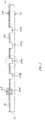
- the assembly 100 may include a substrate 102 including a plurality of vias 104A-104E formed therein.
- the substrate may include a first main side 106 opposite a second main side 108, a first end 110 opposite a second end 112, and a first side 114 opposite a second side 116.
- the substrate 102 may be a flexible printed circuit board (PCB), such as a flexible polymer substrate having stable dimensions under a given temperature that causes PTC change.
- PCB flexible printed circuit board
- EVA ethylene vinyl acetate
- PET polyethylene terephthalate
- PFA Perfluoroalkoxy
- PVDF polyvinylidene difluoride
- the assembly 100 may further include a trace 120 formed along the substrate 102, e.g., atop the first main side 106.
- the trace 120 extends between two or more of the plurality of vias 104A-104E. Although non-limiting, the trace 120 may have multiple paths or legs that end at conductive tabs 122A-122B, as shown.
- the trace 120 is a thin, conductive wire made from silver or copper, or a low thermal conductivity alloy, e.g., Alloy 52.
- a barrier layer 128, such as an electromagnetic interference ink (EMI) or a polymer film, may be formed over the first main side 106 of the substrate 102, including atop the trace 120. The barrier layer 128 may prevent signal interference from various power sources (not shown) in proximity thereto.
- EMI electromagnetic interference ink
- the assembly 100 may further include one or more a SMDs 125 disposed within the plurality of vias 104A-104E.
- the SMDs 125 may be protection components and/or sensors including, but not limited to, fuses, PTCs, NTCs, ICs, Reed sensors, MOSFETS, resistors, and capacitors.
- ICs and sensors are considered to be active protection components
- PTCs, NTCs, and fuses are considered to be passive components. It will be appreciated, however, that this arrangement is non-limiting, and the number and configuration of SMDs may vary depending on the application.
- the SMDs 125 may be connected by the trace 120.
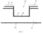
- the via 104C may be recessed into the first main side 106 of the substrate 102.
- the via 104C may extend partially or entirely through the substrate 102.
- the via 104C may include an adhesive layer 130 deposited/formed along an inner surface 133 thereof.
- the adhesive layer 130 may be a polymer adhesive operable to secure the SMDs within the via 104C.
- the via 104C may be lined with a thermally conductive material, such as copper. It will be appreciated that the via 104C provides a conductive path between the trace 120 and the SMD.
- FIGs. 4A-4C demonstrate different trace arrangements according to various embodiments of the present disclosure.
- a first trace 120A includes a lead line 132 connected with a first set of fingers 134, 135.
- a second trace 120B includes a lead line 138 connected with a second set of fingers 140, 142.
- the first set of fingers 134, 135 and the second set of fingers 140, 142 may be interleaved with respect to one another and connected by a conductive pad (not shown).
- the lead lines 132, 138 may be a highly conductive material, such as silver or copper, while the first set of fingers 134, 135 and the second set of fingers 140, 142 may be a low expansion, low thermal conductivity material, such as Alloy 52.
- a first trace 220A includes a lead line 232 connected with a first set of fingers 234, 235, 236.
- a second trace 220B includes a lead line 238 connected with a second set of fingers 240, 241, 242.
- the first set of fingers 234-236 and the second set of fingers 240-242 may be interdigitated with respect to one another and connected by a conductive pad (not shown).
- the lead lines 232, 238 may be a highly conductive material, such as silver or copper, while the first set of fingers 234-236 and the second set of fingers 240-242 may be a low expansion, low thermal conductivity material, such as Alloy 52.
- a first trace 320A includes a lead line 332 connected with a first set of fingers 334, 335.
- fingers 334, 335 extend perpendicular to the lead line 332.
- a second trace 320B includes a lead line 338 connected with a second set of fingers 340 and 341, wherein the lead line 338 and the second set of fingers 340, 341 extend perpendicular to one another.
- the first set of fingers 334, 335 and the second set of fingers 340, 341 are not interwoven or interdigitated with respect to one another. Instead the first set of fingers 334, 335 and the second set of fingers 340, 341 generally extend parallel to one another.
- the method 400 may include providing a plurality of vias through a substrate.
- the substrate may be a flexible PCB made from PET or PI.
- the method 400 may further include forming a trace atop the substrate, the trace extending between each of the plurality of vias.
- the trace includes a lead line connected with a set of fingers.
- the lead line is made from silver or copper, and the set of fingers is made from alloy 52.
- a barrier layer may then be formed over the trace and the substrate, wherein the barrier layer is an electromagnetic interference ink or a polymer film.
- the method 400 may further include positioning a surface mounted device within a via of the plurality of vias.
- a polymer adhesive layer is formed along an inner surface of one or more of the vias.
- the surface mounted device(s) may include protection components and/or sensors including, but not limited to, fuses, PTCs, NTCs, ICs, Reed sensors, MOSFETS, resistors, and capacitors.
- the illustrative method 400 is described above as a series of acts or events, the present disclosure is not limited by the illustrated ordering of such acts or events unless specifically stated. For example, some acts may occur in different orders and/or concurrently with other acts or events apart from those illustrated and/or described herein, in accordance with the disclosure. In addition, not all illustrated acts or events may be required to implement a methodology in accordance with the present disclosure. Furthermore, the method 400 may be implemented in association with the formation and/or processing of structures illustrated and described herein as well as in association with other structures not illustrated.
- the terms “substantial” or “substantially,” as well as the terms “approximate” or “approximately,” can be used interchangeably in some embodiments, and can be described using any relative measures acceptable by one of ordinary skill in the art. For example, these terms can serve as a comparison to a reference parameter, to indicate a deviation capable of providing the intended function. Although non-limiting, the deviation from the reference parameter can be, for example, in an amount of less than 1%, less than 3%, less than 5%, less than 10%, less than 15%, less than 20%, and so on.
- design tools can be provided and configured to create the datasets used to pattern the layers of the grating material and the diffracted optical elements described herein. For example, data sets can be created to generate photomasks used during lithography operations to pattern the layers for structures as described herein.
- Such design tools can include a collection of one or more modules and can also be comprised of hardware, software or a combination thereof.
- a tool can be a collection of one or more software modules, hardware modules, software/hardware modules or any combination or permutation thereof.
- a tool can be a computing device or other appliance running software, or implemented in hardware.
Landscapes
- Engineering & Computer Science (AREA)
- Microelectronics & Electronic Packaging (AREA)
- Manufacturing & Machinery (AREA)
- Physics & Mathematics (AREA)
- Electromagnetism (AREA)
- Structure Of Printed Boards (AREA)
- Parts Printed On Printed Circuit Boards (AREA)
Abstract
Description
- The disclosure relates generally to surface mounted devices (SMDs), and more particularly, to a flexible harness assembly for SMDs.
- Surface mounted devices (SMDs) and sensors, such as negative/positive temperature coefficient sensors, reed switches, Anisotropic Magneto-Resistance (AMR) Giant Magneto-Resistance (GMR) sensors, Tunnel Magneto-Resistance (TMR) sensors, and/or fuses, or their combination, require connection to a control circuit. One conventional assembly approach includes placing sensors on a printed circuit board (PCB) and connecting the sensors by wires afterwards. In some cases, wire harnesses are also employed to carry out the connection. However, wire harnessing can be expensive. Therefore, how to wire one or more devices, such as SMDs or sensors, without the use of conventional wire harnesses, is a critical problem to be addressed.
- This Summary is provided to introduce a selection of concepts in a simplified form that are further described below in the Detailed Description. This Summary is not intended to identify key features or essential features of the claimed subject matter, nor is it intended as an aid in determining the scope of the claimed subject matter.
- In view of the foregoing, what is needed is a universal flexible harness for SMDs and/or sensors connected by a trace line.
- In one approach, a harness assembly may include a substrate having a plurality of vias, and a trace formed atop the substrate, the trace extending between each of the plurality of vias. The harness assembly may further include a surface mounted device disposed within a via of the plurality of vias.
- In another approach, an assembly may include a substrate having a plurality of vias, and a trace formed atop the substrate, the trace extending between each of the plurality of vias. The assembly may further include a surface mounted device disposed within a via of the plurality of vias, the surface mounted device electrically connected with the trace.
- In yet another approach, a method for forming a harness assembly may include providing a plurality of vias through a substrate, and forming a trace atop the substrate, the trace extending between each of the plurality of vias. The method may further include positioning a surface mounted device within a via of the plurality of vias.
- The accompanying drawings illustrate approaches of the disclosed embodiments so far devised for the practical application of the principles thereof, and in which:
-
FIG. 1 is a top view of a harness assembly according to an approach of the disclosure; -
FIG. 2 is side cross-sectional view of the device ofFIG. 1 along cutline 2-2 according to an approach of the disclosure; -
FIG. 3 is a side cross-sectional view of an opening in the device ofFIG. 2 according to an approach of the disclosure; -
FIGs. 4A-4C depict various trace connections according to approaches of the disclosure; and -
FIG. 5 depicts a method according to an approach of the disclosure. - The drawings are not necessarily to scale. The drawings are merely representations, not intended to portray specific parameters of the disclosure. The drawings are intended to depict typical embodiments of the disclosure, and therefore should not be considered as limiting in scope. In the drawings, like numbering represents like elements.
- Furthermore, certain elements in some of the figures may be omitted, or illustrated not-to-scale, for illustrative clarity. Furthermore, for clarity, some reference numbers may be omitted in certain drawings.
- Embodiments in accordance with the present disclosure will now be described more fully hereinafter with reference to the accompanying drawings. Assemblies and methods of the disclosure may be embodied in many different forms and should not be construed as being limited to the embodiments set forth herein. Rather, these embodiments are provided so that this disclosure will be thorough and complete, and will fully convey the scope of the system and method to those skilled in the art.
- Embodiments herein provide an economical solution for low current carrying applications using a trace line connection to a flexible electronically conducting line deposited on a substrate. In some embodiments, the substrate, which may be flexible, has preset tabs or vias where SMD, such as sensors or fuses, can be attached. The advantage of this design is that long lead wires, sometimes required for the sensors, can be easily attached either manually or by automated line in a reflow furnace. The flatness and robustness of the design allows sensors to be placed in tight spots where cross-section of the device placement is limited. Moreover, in some embodiments, the leads may be overprinted with electromagnetic interference ink (EMI) or a polymer film to prevent signal interference from power sources. The design may be especially robust in places where vibration can otherwise affect the robustness of the joints, as flexible lines have a much lower young modulus than wire. Although non-limiting, some possible uses for this design include NTC leads to a controller, or a reed connection to feedback in appliances, car designs, or securities. Moreover, because the material for low thermal conductivity can have magnetic properties, the design can behave as a magnetic flux concentrator.
- Turning now to
FIGS. 1-2 , illustrated is an embodiment of a harness device or assembly 100 in accordance with the present disclosure. As shown, the assembly 100 may include asubstrate 102 including a plurality ofvias 104A-104E formed therein. The substrate may include a firstmain side 106 opposite a secondmain side 108, afirst end 110 opposite asecond end 112, and afirst side 114 opposite a second side 116. In some embodiments, thesubstrate 102 may be a flexible printed circuit board (PCB), such as a flexible polymer substrate having stable dimensions under a given temperature that causes PTC change. For example, for ethylene vinyl acetate (EVA), it could be polyethylene terephthalate (PET) or polypropylene PTC with PFA (Perfluoroalkoxy) substrate, or PTC with polyvinylidene difluoride (PVDF) and a polyimide substrate. - The assembly 100 may further include a
trace 120 formed along thesubstrate 102, e.g., atop the firstmain side 106. Thetrace 120 extends between two or more of the plurality ofvias 104A-104E. Although non-limiting, thetrace 120 may have multiple paths or legs that end atconductive tabs 122A-122B, as shown. In some embodiments, thetrace 120 is a thin, conductive wire made from silver or copper, or a low thermal conductivity alloy, e.g., Alloy 52. In some embodiments, abarrier layer 128, such as an electromagnetic interference ink (EMI) or a polymer film, may be formed over the firstmain side 106 of thesubstrate 102, including atop thetrace 120. Thebarrier layer 128 may prevent signal interference from various power sources (not shown) in proximity thereto. - The assembly 100 may further include one or more a
SMDs 125 disposed within the plurality ofvias 104A-104E. In various embodiments, theSMDs 125 may be protection components and/or sensors including, but not limited to, fuses, PTCs, NTCs, ICs, Reed sensors, MOSFETS, resistors, and capacitors. Of these protection components, ICs and sensors are considered to be active protection components, while PTCs, NTCs, and fuses are considered to be passive components. It will be appreciated, however, that this arrangement is non-limiting, and the number and configuration of SMDs may vary depending on the application. TheSMDs 125 may be connected by thetrace 120. - Turning now to
FIG. 3 , via 104C according to embodiments of the present disclosure will be described in greater detail. As shown, the via 104C may be recessed into the firstmain side 106 of thesubstrate 102. In various embodiments, the via 104C may extend partially or entirely through thesubstrate 102. The via 104C may include anadhesive layer 130 deposited/formed along an inner surface 133 thereof. In some embodiments, theadhesive layer 130 may be a polymer adhesive operable to secure the SMDs within the via 104C. In other embodiments, the via 104C may be lined with a thermally conductive material, such as copper. It will be appreciated that the via 104C provides a conductive path between thetrace 120 and the SMD. -
FIGs. 4A-4C demonstrate different trace arrangements according to various embodiments of the present disclosure. As shown inFIG. 4A , a first trace 120A includes alead line 132 connected with a first set offingers second trace 120B includes alead line 138 connected with a second set offingers fingers fingers fingers fingers - As shown in
FIG. 4B , afirst trace 220A includes alead line 232 connected with a first set offingers fingers - As shown in
FIG. 4C , afirst trace 320A includes alead line 332 connected with a first set offingers fingers lead line 332. Similarly, asecond trace 320B includes alead line 338 connected with a second set offingers 340 and 341, wherein thelead line 338 and the second set offingers 340, 341 extend perpendicular to one another. As shown, the first set offingers fingers 340, 341 are not interwoven or interdigitated with respect to one another. Instead the first set offingers fingers 340, 341 generally extend parallel to one another. - Turning now to
FIG. 5 , amethod 400 to form a harness assembly according to embodiments of the present disclosure will be described. Atblock 401, themethod 400 may include providing a plurality of vias through a substrate. In some embodiments, the substrate may be a flexible PCB made from PET or PI. - At
block 402, themethod 400 may further include forming a trace atop the substrate, the trace extending between each of the plurality of vias. In some embodiments, the trace includes a lead line connected with a set of fingers. In some embodiments, the lead line is made from silver or copper, and the set of fingers is made from alloy 52. In some embodiments, a barrier layer may then be formed over the trace and the substrate, wherein the barrier layer is an electromagnetic interference ink or a polymer film. - At
block 403, themethod 400 may further include positioning a surface mounted device within a via of the plurality of vias. In some embodiments, a polymer adhesive layer is formed along an inner surface of one or more of the vias. In some embodiments, the surface mounted device(s) may include protection components and/or sensors including, but not limited to, fuses, PTCs, NTCs, ICs, Reed sensors, MOSFETS, resistors, and capacitors. - Although the
illustrative method 400 is described above as a series of acts or events, the present disclosure is not limited by the illustrated ordering of such acts or events unless specifically stated. For example, some acts may occur in different orders and/or concurrently with other acts or events apart from those illustrated and/or described herein, in accordance with the disclosure. In addition, not all illustrated acts or events may be required to implement a methodology in accordance with the present disclosure. Furthermore, themethod 400 may be implemented in association with the formation and/or processing of structures illustrated and described herein as well as in association with other structures not illustrated. - As used herein, an element or operation recited in the singular and proceeded with the word "a" or "an" is to be understood as including plural elements or operations, until such exclusion is explicitly recited. Furthermore, references to "one embodiment" of the present disclosure are not intended as limiting. Additional embodiments may also incorporate the recited features.
- Furthermore, the terms "substantial" or "substantially," as well as the terms "approximate" or "approximately," can be used interchangeably in some embodiments, and can be described using any relative measures acceptable by one of ordinary skill in the art. For example, these terms can serve as a comparison to a reference parameter, to indicate a deviation capable of providing the intended function. Although non-limiting, the deviation from the reference parameter can be, for example, in an amount of less than 1%, less than 3%, less than 5%, less than 10%, less than 15%, less than 20%, and so on.
- Still furthermore, one of ordinary skill will understand when an element such as a layer, region, or substrate is referred to as being formed on, deposited on, or disposed "on," "over" or "atop" another element, the element can be directly on the other element or intervening elements may also be present. In contrast, when an element is referred to as being "directly on," "directly over" or "directly atop" another element, no intervening elements are present.
- In various embodiments, design tools can be provided and configured to create the datasets used to pattern the layers of the grating material and the diffracted optical elements described herein. For example, data sets can be created to generate photomasks used during lithography operations to pattern the layers for structures as described herein. Such design tools can include a collection of one or more modules and can also be comprised of hardware, software or a combination thereof. Thus, for example, a tool can be a collection of one or more software modules, hardware modules, software/hardware modules or any combination or permutation thereof. As another example, a tool can be a computing device or other appliance running software, or implemented in hardware.
- The present disclosure is not to be limited in scope by the specific embodiments described herein. Indeed, other various embodiments of and modifications to the present disclosure, in addition to those described herein, will be apparent to those of ordinary skill in the art from the foregoing description and accompanying drawings. Thus, such other embodiments and modifications are intended to fall within the scope of the present disclosure. Furthermore, the present disclosure has been described herein in the context of a particular implementation in a particular environment for a particular purpose. Those of ordinary skill in the art will recognize the usefulness is not limited thereto and the present disclosure may be beneficially implemented in any number of environments for any number of purposes. Thus, the claims set forth below are to be construed in view of the full breadth and spirit of the present disclosure as described herein.
Claims (13)
- A harness assembly, comprising:a substrate including a plurality of vias;a trace formed atop the substrate, the trace extending between each of the plurality of vias; anda surface mounted device disposed within a via of the plurality of vias.
- The harness assembly of claim 1, wherein the trace including a lead line connected with a set of fingers.
- The harness assembly of claim 2, wherein the lead line has a first conductivity and the set of fingers has a second conductivity, less than the first conductivity.
- The harness assembly of claim 2, wherein the lead line is made from silver or copper, and the set of fingers is made from alloy 52.
- The harness assembly of claim 1, wherein the surface mounted device is a positive temperature coefficient material sensor, a negative temperature coefficient material sensor, a magnetoresistance sensor, or a reed switch.
- The harness assembly of claim 1, further comprising a barrier layer formed over the trace.
- The harness assembly of claim 6, wherein the barrier layer is an electromagnetic interference ink or a polymer film.
- The harness assembly of claim 1, wherein the substrate is a printed circuit board.
- The harness assembly of claim 1, further comprising an adhesive layer within the via.
- A method for forming a harness assembly, the method comprising:providing a plurality of vias through a substrate;forming a trace atop the substrate, the trace extending between each of the plurality of vias; andpositioning a surface mounted device within a via of the plurality of vias.
- The method of claim 10, further comprising a barrier layer formed over the trace, wherein the barrier layer is an electromagnetic interference ink or a polymer film.
- The method of claim 10, further comprising coupling a lead line of the trace with a set of fingers.
- The method of claim 10, further comprising providing an adhesive layer along an inner surface of the via, wherein the substrate is a printed circuit board.
Applications Claiming Priority (1)
| Application Number | Priority Date | Filing Date | Title |
|---|---|---|---|
| US16/893,735 US10980115B1 (en) | 2020-06-05 | 2020-06-05 | Flexible harness assembly for surface mounted devices |
Publications (1)
| Publication Number | Publication Date |
|---|---|
| EP3920673A1 true EP3920673A1 (en) | 2021-12-08 |
Family
ID=75394256
Family Applications (1)
| Application Number | Title | Priority Date | Filing Date |
|---|---|---|---|
| EP21169476.5A Pending EP3920673A1 (en) | 2020-06-05 | 2021-04-20 | Flexible harness assembly for surface mounted devices |
Country Status (4)
| Country | Link |
|---|---|
| US (1) | US10980115B1 (en) |
| EP (1) | EP3920673A1 (en) |
| KR (1) | KR20210151673A (en) |
| CN (1) | CN113764123B (en) |
Citations (3)
| Publication number | Priority date | Publication date | Assignee | Title |
|---|---|---|---|---|
| US5615087A (en) * | 1994-08-18 | 1997-03-25 | Allen-Bradley Company, Inc. | Insulated surface mount circuit board construction |
| EP0774888A2 (en) * | 1995-11-16 | 1997-05-21 | Matsushita Electric Industrial Co., Ltd | Printing wiring board and assembly of the same |
| US20170273171A1 (en) * | 2016-03-16 | 2017-09-21 | Patrick Codd | Flexible printed circuit with radio frequency choke |
Family Cites Families (6)
| Publication number | Priority date | Publication date | Assignee | Title |
|---|---|---|---|---|
| US5090116A (en) * | 1990-12-21 | 1992-02-25 | Amp Incorporated | Method of assembling a connector to a circuit element and soldering lead frame for use therein |
| US5384691A (en) * | 1993-01-08 | 1995-01-24 | General Electric Company | High density interconnect multi-chip modules including embedded distributed power supply elements |
| US6034712A (en) * | 1996-06-26 | 2000-03-07 | Brother Kogyo Kabushiki Kaisha | Exposure apparatus and image forming machine including it |
| US5994648A (en) * | 1997-03-27 | 1999-11-30 | Ford Motor Company | Three-dimensional molded sockets for mechanical and electrical component attachment |
| US7113179B2 (en) * | 2004-06-23 | 2006-09-26 | Interlink Electronics, Inc. | Force sensing resistor with calibration element and method of manufacturing same |
| US7806731B2 (en) * | 2005-12-29 | 2010-10-05 | Sandisk Corporation | Rounded contact fingers on substrate/PCB for crack prevention |
-
2020
- 2020-06-05 US US16/893,735 patent/US10980115B1/en active Active
-
2021
- 2021-03-12 KR KR1020210032503A patent/KR20210151673A/en active Pending
- 2021-03-30 CN CN202110341471.9A patent/CN113764123B/en active Active
- 2021-04-20 EP EP21169476.5A patent/EP3920673A1/en active Pending
Patent Citations (3)
| Publication number | Priority date | Publication date | Assignee | Title |
|---|---|---|---|---|
| US5615087A (en) * | 1994-08-18 | 1997-03-25 | Allen-Bradley Company, Inc. | Insulated surface mount circuit board construction |
| EP0774888A2 (en) * | 1995-11-16 | 1997-05-21 | Matsushita Electric Industrial Co., Ltd | Printing wiring board and assembly of the same |
| US20170273171A1 (en) * | 2016-03-16 | 2017-09-21 | Patrick Codd | Flexible printed circuit with radio frequency choke |
Also Published As
| Publication number | Publication date |
|---|---|
| CN113764123B (en) | 2026-04-17 |
| US10980115B1 (en) | 2021-04-13 |
| KR20210151673A (en) | 2021-12-14 |
| CN113764123A (en) | 2021-12-07 |
Similar Documents
| Publication | Publication Date | Title |
|---|---|---|
| CN104813419B (en) | Thermistor device | |
| GB2545329A (en) | Applying pressure to adhesive using CTE mismatch between components | |
| JP2010165780A (en) | Method of manufacturing thin film resistance element | |
| JP2017502470A5 (en) | ||
| WO2009011419A1 (en) | Device having electronic component mounted therein and method for manufacturing such device | |
| CN101662894A (en) | Encapsulating base plate and encapsulating structure | |
| JP2016004886A (en) | Resistor for current detection | |
| US20150370347A1 (en) | Touch panel using touch pen and formed with power pattern | |
| JP2009052898A (en) | Current detection board | |
| EP3121496B1 (en) | Positioner | |
| US10980115B1 (en) | Flexible harness assembly for surface mounted devices | |
| TWI453870B (en) | Wiring circuit substrate and method of manufacturing same | |
| JP2011185701A (en) | Mounting structure of temperature detection element | |
| US9485850B2 (en) | Circuit device and method of manufacturing the same | |
| JP2008180633A (en) | Substrate for sensor element | |
| CN109406859B (en) | Current detection plate and drive controller | |
| US12069796B2 (en) | Storage device unit | |
| CN109196318A (en) | Hot-fluid measurement device | |
| CN1157595C (en) | Sensor Compensation Components | |
| JP5966767B2 (en) | Circuit board for vehicle control | |
| JP2012129389A (en) | Printed wiring board and manufacturing method of the same | |
| WO2026021170A1 (en) | Flexible circuit plate, circuit board assembly, temperature detection apparatus, and electronic device | |
| JP2009099837A5 (en) | ||
| CN101221597B (en) | Method and device for improving graph pattern matching precision in PCB | |
| JP2004205331A (en) | Magnetic detection device and electronic equipment with magnetic detection function |
Legal Events
| Date | Code | Title | Description |
|---|---|---|---|
| PUAI | Public reference made under article 153(3) epc to a published international application that has entered the european phase |
Free format text: ORIGINAL CODE: 0009012 |
|
| STAA | Information on the status of an ep patent application or granted ep patent |
Free format text: STATUS: THE APPLICATION HAS BEEN PUBLISHED |
|
| AK | Designated contracting states |
Kind code of ref document: A1 Designated state(s): AL AT BE BG CH CY CZ DE DK EE ES FI FR GB GR HR HU IE IS IT LI LT LU LV MC MK MT NL NO PL PT RO RS SE SI SK SM TR |
|
| B565 | Issuance of search results under rule 164(2) epc |
Effective date: 20211025 |
|
| STAA | Information on the status of an ep patent application or granted ep patent |
Free format text: STATUS: REQUEST FOR EXAMINATION WAS MADE |
|
| 17P | Request for examination filed |
Effective date: 20220608 |
|
| RBV | Designated contracting states (corrected) |
Designated state(s): AL AT BE BG CH CY CZ DE DK EE ES FI FR GB GR HR HU IE IS IT LI LT LU LV MC MK MT NL NO PL PT RO RS SE SI SK SM TR |
|
| STAA | Information on the status of an ep patent application or granted ep patent |
Free format text: STATUS: EXAMINATION IS IN PROGRESS |
|
| 17Q | First examination report despatched |
Effective date: 20240917 |