EP3920420A1 - Fast-locking phase-locked loop and associated fast-locking method thereof - Google Patents
Fast-locking phase-locked loop and associated fast-locking method thereof Download PDFInfo
- Publication number
- EP3920420A1 EP3920420A1 EP21151622.4A EP21151622A EP3920420A1 EP 3920420 A1 EP3920420 A1 EP 3920420A1 EP 21151622 A EP21151622 A EP 21151622A EP 3920420 A1 EP3920420 A1 EP 3920420A1
- Authority
- EP
- European Patent Office
- Prior art keywords
- capacitor
- another
- capacitance
- bandwidth
- fast
- Prior art date
- Legal status (The legal status is an assumption and is not a legal conclusion. Google has not performed a legal analysis and makes no representation as to the accuracy of the status listed.)
- Granted
Links
Images


Classifications
-
- H—ELECTRICITY
- H03—ELECTRONIC CIRCUITRY
- H03L—AUTOMATIC CONTROL, STARTING, SYNCHRONISATION OR STABILISATION OF GENERATORS OF ELECTRONIC OSCILLATIONS OR PULSES
- H03L7/00—Automatic control of frequency or phase; Synchronisation
- H03L7/06—Automatic control of frequency or phase; Synchronisation using a reference signal applied to a frequency- or phase-locked loop
- H03L7/08—Details of the phase-locked loop
- H03L7/10—Details of the phase-locked loop for assuring initial synchronisation or for broadening the capture range
- H03L7/107—Details of the phase-locked loop for assuring initial synchronisation or for broadening the capture range using a variable transfer function for the loop, e.g. low pass filter having a variable bandwidth
- H03L7/1075—Details of the phase-locked loop for assuring initial synchronisation or for broadening the capture range using a variable transfer function for the loop, e.g. low pass filter having a variable bandwidth by changing characteristics of the loop filter, e.g. changing the gain, changing the bandwidth
-
- H—ELECTRICITY
- H03—ELECTRONIC CIRCUITRY
- H03L—AUTOMATIC CONTROL, STARTING, SYNCHRONISATION OR STABILISATION OF GENERATORS OF ELECTRONIC OSCILLATIONS OR PULSES
- H03L7/00—Automatic control of frequency or phase; Synchronisation
- H03L7/06—Automatic control of frequency or phase; Synchronisation using a reference signal applied to a frequency- or phase-locked loop
- H03L7/08—Details of the phase-locked loop
- H03L7/10—Details of the phase-locked loop for assuring initial synchronisation or for broadening the capture range
-
- H—ELECTRICITY
- H03—ELECTRONIC CIRCUITRY
- H03L—AUTOMATIC CONTROL, STARTING, SYNCHRONISATION OR STABILISATION OF GENERATORS OF ELECTRONIC OSCILLATIONS OR PULSES
- H03L7/00—Automatic control of frequency or phase; Synchronisation
- H03L7/06—Automatic control of frequency or phase; Synchronisation using a reference signal applied to a frequency- or phase-locked loop
- H03L7/08—Details of the phase-locked loop
-
- H—ELECTRICITY
- H03—ELECTRONIC CIRCUITRY
- H03F—AMPLIFIERS
- H03F3/00—Amplifiers with only discharge tubes or only semiconductor devices as amplifying elements
- H03F3/45—Differential amplifiers
- H03F3/45071—Differential amplifiers with semiconductor devices only
- H03F3/45076—Differential amplifiers with semiconductor devices only characterised by the way of implementation of the active amplifying circuit in the differential amplifier
- H03F3/45179—Differential amplifiers with semiconductor devices only characterised by the way of implementation of the active amplifying circuit in the differential amplifier using MOSFET transistors as the active amplifying circuit
- H03F3/45183—Long tailed pairs
-
- H—ELECTRICITY
- H03—ELECTRONIC CIRCUITRY
- H03F—AMPLIFIERS
- H03F3/00—Amplifiers with only discharge tubes or only semiconductor devices as amplifying elements
- H03F3/45—Differential amplifiers
- H03F3/45071—Differential amplifiers with semiconductor devices only
- H03F3/45076—Differential amplifiers with semiconductor devices only characterised by the way of implementation of the active amplifying circuit in the differential amplifier
- H03F3/45475—Differential amplifiers with semiconductor devices only characterised by the way of implementation of the active amplifying circuit in the differential amplifier using IC blocks as the active amplifying circuit
-
- H—ELECTRICITY
- H03—ELECTRONIC CIRCUITRY
- H03F—AMPLIFIERS
- H03F3/00—Amplifiers with only discharge tubes or only semiconductor devices as amplifying elements
- H03F3/45—Differential amplifiers
- H03F3/45071—Differential amplifiers with semiconductor devices only
- H03F3/45479—Differential amplifiers with semiconductor devices only characterised by the way of common mode signal rejection
- H03F3/45632—Differential amplifiers with semiconductor devices only characterised by the way of common mode signal rejection in differential amplifiers with FET transistors as the active amplifying circuit
- H03F3/45744—Differential amplifiers with semiconductor devices only characterised by the way of common mode signal rejection in differential amplifiers with FET transistors as the active amplifying circuit by offset reduction
- H03F3/45748—Differential amplifiers with semiconductor devices only characterised by the way of common mode signal rejection in differential amplifiers with FET transistors as the active amplifying circuit by offset reduction by using a feedback circuit
- H03F3/45753—Differential amplifiers with semiconductor devices only characterised by the way of common mode signal rejection in differential amplifiers with FET transistors as the active amplifying circuit by offset reduction by using a feedback circuit using switching means, e.g. sample and hold
-
- H—ELECTRICITY
- H03—ELECTRONIC CIRCUITRY
- H03F—AMPLIFIERS
- H03F3/00—Amplifiers with only discharge tubes or only semiconductor devices as amplifying elements
- H03F3/45—Differential amplifiers
- H03F3/45071—Differential amplifiers with semiconductor devices only
- H03F3/45479—Differential amplifiers with semiconductor devices only characterised by the way of common mode signal rejection
- H03F3/45928—Differential amplifiers with semiconductor devices only characterised by the way of common mode signal rejection using IC blocks as the active amplifying circuit
- H03F3/45968—Differential amplifiers with semiconductor devices only characterised by the way of common mode signal rejection using IC blocks as the active amplifying circuit by offset reduction
- H03F3/45973—Differential amplifiers with semiconductor devices only characterised by the way of common mode signal rejection using IC blocks as the active amplifying circuit by offset reduction by using a feedback circuit
- H03F3/45977—Differential amplifiers with semiconductor devices only characterised by the way of common mode signal rejection using IC blocks as the active amplifying circuit by offset reduction by using a feedback circuit using switching means, e.g. sample and hold
-
- H—ELECTRICITY
- H03—ELECTRONIC CIRCUITRY
- H03L—AUTOMATIC CONTROL, STARTING, SYNCHRONISATION OR STABILISATION OF GENERATORS OF ELECTRONIC OSCILLATIONS OR PULSES
- H03L7/00—Automatic control of frequency or phase; Synchronisation
- H03L7/06—Automatic control of frequency or phase; Synchronisation using a reference signal applied to a frequency- or phase-locked loop
- H03L7/08—Details of the phase-locked loop
- H03L7/085—Details of the phase-locked loop concerning mainly the frequency- or phase-detection arrangement including the filtering or amplification of its output signal
- H03L7/087—Details of the phase-locked loop concerning mainly the frequency- or phase-detection arrangement including the filtering or amplification of its output signal using at least two phase detectors or a frequency and phase detector in the loop
-
- H—ELECTRICITY
- H03—ELECTRONIC CIRCUITRY
- H03L—AUTOMATIC CONTROL, STARTING, SYNCHRONISATION OR STABILISATION OF GENERATORS OF ELECTRONIC OSCILLATIONS OR PULSES
- H03L7/00—Automatic control of frequency or phase; Synchronisation
- H03L7/06—Automatic control of frequency or phase; Synchronisation using a reference signal applied to a frequency- or phase-locked loop
- H03L7/08—Details of the phase-locked loop
- H03L7/085—Details of the phase-locked loop concerning mainly the frequency- or phase-detection arrangement including the filtering or amplification of its output signal
- H03L7/093—Details of the phase-locked loop concerning mainly the frequency- or phase-detection arrangement including the filtering or amplification of its output signal using special filtering or amplification characteristics in the loop
-
- H—ELECTRICITY
- H03—ELECTRONIC CIRCUITRY
- H03L—AUTOMATIC CONTROL, STARTING, SYNCHRONISATION OR STABILISATION OF GENERATORS OF ELECTRONIC OSCILLATIONS OR PULSES
- H03L7/00—Automatic control of frequency or phase; Synchronisation
- H03L7/06—Automatic control of frequency or phase; Synchronisation using a reference signal applied to a frequency- or phase-locked loop
- H03L7/16—Indirect frequency synthesis, i.e. generating a desired one of a number of predetermined frequencies using a frequency- or phase-locked loop
- H03L7/18—Indirect frequency synthesis, i.e. generating a desired one of a number of predetermined frequencies using a frequency- or phase-locked loop using a frequency divider or counter in the loop
-
- H—ELECTRICITY
- H03—ELECTRONIC CIRCUITRY
- H03L—AUTOMATIC CONTROL, STARTING, SYNCHRONISATION OR STABILISATION OF GENERATORS OF ELECTRONIC OSCILLATIONS OR PULSES
- H03L2207/00—Indexing scheme relating to automatic control of frequency or phase and to synchronisation
- H03L2207/04—Modifications for maintaining constant the phase-locked loop damping factor when other loop parameters change
Definitions
- the present invention is related to phase-locked loop (PLL), and more particularly, to a fast-locking PLL and an associated fast-locking method thereof.
- PLL phase-locked loop
- At least one parameter of the fast-locking PLL can be configured to be variable.
- a charge pump current of a PLL can be dynamically switched during a locking operation of this PLL, thereby accelerate the locking operation without sacrificing noise-related performance of the PLL.
- the charge pump current is controlled to have an initial current that is greater than a final current, where the initial current makes the locking operation faster but the noise-related performance is worse in comparison with having the final current; and when the locking operation is almost completed (e.g. output frequency of the PLL is close to a target frequency), the charge pump current can be controlled to have the final current, in order to guarantee the noise-related performance.
- an objective of the present invention is to provide a fast-locking phase-locked loop (PLL) and an associated fast-locking method thereof, e.g. a fast-locking PLL based on gear-shifting loop filter for dynamic bandwidth control, which can implement a fast-locking operation without greatly increase additional costs.
- PLL phase-locked loop
- the fast-locking PLL may comprise a gear-shifting loop filter which is configured to have a dynamic bandwidth.
- the gear-shifting loop filter may comprise a resistor set and a capacitor set coupled to the resistor set, wherein the resistor set is configured to have a dynamic resistance, and the capacitor set is configured to have a dynamic capacitance.
- the dynamic resistance is switched from a first resistance to a second resistance and the dynamic capacitance is switched from a first capacitance to a second capacitance, to make the dynamic bandwidth be switched from a first bandwidth to a second bandwidth.
- At least one embodiment of the present invention provides a fast-locking method of a fast-locking PLL.
- the fast-locking method may comprise: utilizing a resistor set of a gear-shifting loop filter within the fast-locking PLL to control a dynamic resistance and utilizing a capacitor set of the gear-shifting loop filter to control a dynamic capacitance, to make the gear-shifting loop filter have a dynamic bandwidth; and switching the dynamic resistance from a first resistance to a second resistance, and switching the dynamic capacitance from a first capacitance to a second capacitance, to make the dynamic bandwidth be switched from a first bandwidth to a second bandwidth.
- Embodiments of the present invention can enhance the speed of a locking operation of a PLL without sacrificing the noise-related performance by switching resistance and capacitance(s) of a loop filter within the PLL, which dynamically switches bandwidth of the loop filter during the locking operation.
- the embodiments of the present invention will not greatly increase additional costs.
- the present invention can improve overall performance without introducing any side effect or in a way that is less likely to introduce side effects.
- a phase-locked loop may comprise a phase detector (e.g. a phase frequency detector), a charge pump, a loop filter, a voltage control oscillator (VCO) and a divider.
- a gear-shifting bandwidth e.g. a dynamic bandwidth
- the gear-shifting bandwidth can comprise a first bandwidth and a second bandwidth, which are sequentially adopted during a locking operation of the PLL.
- the first bandwidth is adopted in a first mode
- the second bandwidth is adopted in a second mode following the first mode, where the first bandwidth benefits locking speed (e.g.
- I CP represents a charge pump current of the charge pump
- K VCO represents a VCO gain of the VCO
- R P represents a resistance of a resistor within the loop filter
- C P represents a capacitance of a capacitor within the loop filter
- N represents a divisor of the divider.
- a method of changing a bandwidth e.g. the open loop bandwidth K or the close loop bandwidth ⁇ n
- the damping factor ⁇ may be designed to be unchanged when varying the bandwidth between the first bandwidth and the second bandwidth.
- I CP in the first mode can be designed to be 2 times that in the second mode, and the first bandwidth can be 2 times the second bandwidth if the damping factor ⁇ is unchanged (e.g. R P in the first mode is designed to be 1 / 2 times that in the second mode).
- R P in the first mode is designed to be 1 / 2 times that in the second mode.
- the present invention provides another mechanism to implement the gear-shifting bandwidth.
- R P in the first mode can be designed to be 2 times that in the second mode, and the first bandwidth can be 2 times the second bandwidth if the damping factor ⁇ is unchanged (e.g. C P in the first mode is designed to be 1/4 times that in the second mode).
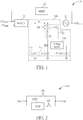
- FIG. 1 is a diagram illustrating a fast-locking PLL 10 according to an embodiment of the present invention, where the fast-locking PLL 10 may be an example of the aforementioned PLL.
- the fast-locking PLL 10 may comprise a gear-shifting loop filter 100, a phase frequency detector with charge pump (which may be referred to as "PFD/CP" for brevity) 11, a voltage control oscillator (VCO) 12 and a divider such as a multi-modulus divider (MMD) 13.
- PFD/CP phase frequency detector with charge pump
- VCO voltage control oscillator
- MMD multi-modulus divider
- the PFD/CP 11 may generate a voltage signal according to phase or frequency difference between a reference clock signal CK REF from a reference clock source (not shown) and a divided clock signal CK MMD from the MMD 13.
- This voltage signal may be transmitted to the VCO 12 via a path coupled to the gear-shifting loop filter.
- the VCO 12 then generates an output clock signal CK VCO according to the received voltage signal, and the MMD 13 may perform a frequency dividing operation upon the output clock signal CK VCO , e.g. a frequency of the output clock signal CK VCO may be divided by a certain value (e.g. an integer of a fractional value greater than one), in order to generate the divided clock signal CK MMD .
- embodiments of the present invention aim at providing implementations of the gear-shifting loop filter 100 (which will be described in detail later), where the other components such as the PFD/CP 11, the VCO 12 and the MMD 13 may be implemented or replaced by any suitable circuit architecture, and related details regarding to these components are omitted here for brevity.
- the architecture of the fast-locking PLL 10 shown in FIG. 1 is for illustrative purpose only, and is not meant to be a limitation of the present invention, that is, the gear-shifting loop filter 100 can be applied to any architecture of a fast-locking PLL which comprises a loop filter comprising resistors and/or capacitors.
- the gear-shifting loop filter 100 may be configured to have a dynamic bandwidth (e.g. either a bandwidth BW1 or a bandwidth BW2) in order to perform a gear-shifting operation (e.g. switching the dynamic bandwidth from the bandwidth BW1 to the bandwidth BW2). More specifically, the gear-shifting loop filter 100 may comprise a capacitor set C S1 , a resistor set R S2 and a capacitor set C S2 coupled to the resistor set R S2 . Assume that the bandwidth BW1 is designed to be ⁇ times the bandwidth BW2 in the embodiment of FIG.1 , where ⁇ is a positive value greater than one. In this embodiment, the resistor set R S2 may be configured to have a fixed capacitance (e.g.
- the resistor set R S2 may be configured to have a dynamic resistance (e.g. either a resistance " ⁇ ⁇ R 2 " or a resistance " R 2 ", which is expressed by italics of the symbol “R 2 "), and the capacitor set C S2 may be configured to have a dynamic capacitance (e.g. either a capacitance " ⁇ ⁇ C 2 " or a capacitance " C 2 ", which is expressed by italics of the symbol “C 2 "), where ⁇ is preferably designed as 1 / ⁇ 2 , but the present invention is not limited thereto.
- the dynamic resistance of the resistor set R S2 and the dynamic capacitance of the capacitor set C S2 may be examples of the resistance R P and the capacitance C P mentioned above, respectively.
- the dynamic resistance of the resistor set R S2 can be switched from “ ⁇ ⁇ R 2 " to " R 2 " and the dynamic capacitance of the capacitor set C S2 can be switched from “ ⁇ ⁇ C 2 " to “C 2 ", to make the dynamic bandwidth be switched from the bandwidth BW1 to the bandwidth BW2.
- the resistor set R S2 is coupled between a first common node such as a node N1 and a second common node such as a node N2 of the gear-shifting loop filter 100.
- the resistor set R S2 may comprises a resistor ( ⁇ -1)R 2 (which has a resistance "( ⁇ - 1) ⁇ R 2 " and a resistor R 2 (which has the resistance " R 2 "), where the resistors ( ⁇ -1)R 2 and R 2 may be coupled in series, and a switch controlled by a gear-shifting control signal ⁇ 2 is coupled across the resistors ( ⁇ -1)R 2 , e.g.
- the dynamic resistance of the resistor set R S2 can be switched from “ ⁇ ⁇ R 2 " to " R 2 " by turning on this switch, but the present invention is not limited thereto.
- the resistor set R S2 having the dynamic resistance may be implemented by different way (e.g. a variable resistor, or multiple resistors with at least one switch for controlling connection of the multiple resistors).
- the capacitor set C S2 may comprise a capacitor ⁇ C 2 (which has the capacitance " ⁇ ⁇ C 2 ”) and a capacitor (1- ⁇ )C 2 (which has a capacitance "(1 - ⁇ ) ⁇ C 2 "), where the capacitor ⁇ C 2 is coupled to the resistor set R S2 via the node N2, and the dynamic capacitance of the capacitor set C S2 can be switched from “ ⁇ ⁇ C 2 " to " C 2 " by coupling the capacitor (1- ⁇ )C 2 to the node N2.
- the capacitor (1- ⁇ )C 2 may be coupled to the node N2 without any processing in advance when performing the gear-shifting operation. This may cause some disadvantage, however. For example, when a locking operation of the fast-locking PLL 10 is almost completed, a voltage level on the node N2 is expected to be around a target level, where a voltage level on the capacitor (1- ⁇ )C 2 may be different from that on the node N2, and therefore the voltage level on the node N2 may be pulled away from this target level when coupling the capacitor (1- ⁇ )C 2 to the node N2. Under this condition, the locking operation will need to spend extra time for recovering the voltage level on the node N2 back to this target level via the bandwidth BW2. As the bandwidth BW2 is designed for optimizing the noise-related performance, and may be relatively disadvantageous on the speed of the locking operation in comparison with the bandwidth BW1, this extra time for recovering the voltage level on the node N2 may be quite long and is therefore unwanted.
- a voltage buffer 110 within the gear-shifting loop filter 100 may be coupled between the node N2 and the capacitor (1- ⁇ )C 2
- FIG. 2 is a diagram illustrating some details of the voltage buffer 110 shown in FIG. 1 according to an embodiment of the present invention.
- An input terminal Vin and an output terminal Vout of the voltage buffer are coupled to the node N2 and the capacitor (1- ⁇ )C 2 shown in FIG. 1 , respectively, and with aid of the voltage buffer 110, a voltage level on the capacitor ⁇ C 2 (or on the node N2) can be copied to the capacitor (1- ⁇ )C 2 before coupling the capacitor (1- ⁇ )C 2 to the node N2.
- FIG. 1 is a diagram illustrating some details of the voltage buffer 110 shown in FIG. 1 according to an embodiment of the present invention.
- An input terminal Vin and an output terminal Vout of the voltage buffer are coupled to the node N2 and the capacitor (1- ⁇ )C 2 shown in FIG. 1 , respectively, and with aid of the voltage buffer 110, a voltage level on the capacitor
- the voltage buffer 110 may comprise a unit gain buffer (UGB) 110U, a first switch controlled by a gear-shifting control signal ⁇ 1, and a second switch controlled by the gear-shifting control signal ⁇ 2.
- UGB 110U and the first switch coupled in series may represent a first signal path between an input terminal Vin and an output terminal Vout of the voltage buffer 110
- the second switch may represent a second signal path between the input terminal Vin and the output terminal Vout of the voltage buffer 110.
- the fast-locking PLL 10 may operate under a first bandwidth mode (which relatively benefits the locking speed), where the first switch is turned on and the second switch is turned off, to enable the first signal path between the input terminal Vin and the output terminal Vout, so the voltage level on the capacitor ⁇ C 2 (or on the node N2) can be copied to the capacitor (1- ⁇ )C 2 by the UGB 110U at certain time point(s) before coupling the capacitor (1- ⁇ )C 2 to the node N2; and after the locking operation is almost completed (e.g.
- the fast-locking PLL 10 may enter a second bandwidth mode (which relatively benefits the noise-related performance) from the first bandwidth mode, where the first switch is turned off and the second switch is turned on, to enable the second signal path between the input terminal Vin and the output terminal Vout, so the capacitor (1- ⁇ )C 2 can be coupled to the node N2, to switch the dynamic bandwidth from the bandwidth BW1 to the bandwidth BW2.
- the present invention is not limited thereto.
- the voltage level on the capacitor (1- ⁇ )C 2 is similar or identical to that on the capacitor ⁇ C 2 , any possible problem that may occur in an embodiment without using the voltage buffer 110 can be solved, and overall performance (e.g. the speed of the locking operation) can be optimized.
- phase margin of the fast-locking PLL may change.
- the phase margin can be kept unchanged with aid of switching the capacitor set C S1 shown in FIG. 1 , to optimize the overall performance of a fast-locking PLL.
- a bandwidth ⁇ C e.g. the bandwidth BW2 mentioned above
- a zero frequency ⁇ Z e.g. the bandwidth BW2 mentioned above
- a pole frequency ⁇ P e.g. the pole frequency ⁇ P
- phase margin ⁇ ( ⁇ ) with respect to a frequency variable ⁇ of a fast-locking PLL (e.g. the fast-locking PLL 10 shown in FIG.
- phase margin ⁇ ( ⁇ ) of this fast-locking PLL operating under the first bandwidth mode is preferably the same as that operating under the second bandwidth mode.
- phase margin ⁇ ( ⁇ ) i.e.
- FIG. 3 is a diagram illustrating a fast-locking PLL 30 according to an embodiment of the present invention, where the fast-locking PLL 30 may be obtained by modifying the architecture of the fast-locking PLL 10 shown in FIG. 1 , and more particularly, by modifying implementation of the capacitor set C S1 .
- the capacitor set Csi may comprise a capacitor ⁇ C 1 (which has the capacitance " ⁇ ⁇ C 1 ”) and a capacitor (1- ⁇ )C 1 (which has a capacitance "(1 - ⁇ ) ⁇ C 1 "), where the capacitor ⁇ C 1 is coupled to the node N1.
- the dynamic capacitance of the capacitor set Csi can be switched from “ ⁇ ⁇ C 1 " to " C 1 " by coupling the capacitor (1- ⁇ )C 1 to the node N1, to make the phase margin of the fast-locking PLL 30 unchanged.
- the capacitor (1- ⁇ )C 1 may be coupled to the node N1 without any processing in advance when performing the gear-shifting operation. Due to the similar reason mentioned above, this may cause some disadvantage. For example, when a locking operation of the fast-locking PLL 30 is almost completed, a voltage level on the node N1 is expected to be around a target level, where a voltage level on the capacitor (1- ⁇ )C 1 may be different from that on the node N1, and therefore the voltage level on the node N1 may be pulled away from this target level when coupling the capacitor (1- ⁇ )C 1 to the node N1. Thus, the locking operation will need to spend extra time for recovering the voltage level on the node N1 back to this target level via the bandwidth BW2.
- a voltage buffer 120 within the gear-shifting loop filter 100 may be coupled between the node N1 and the capacitor (1- ⁇ )C 1 in the embodiment of FIG. 3 .
- the voltage level on the capacitor ⁇ C 1 can be copied to the capacitor (1- ⁇ )C 1 before coupling the capacitor (1- ⁇ )C 1 to the node N1.
- the implementation of the voltage buffer 120 may be similar or identical to the voltage buffer 110, where implementation details of the voltage buffer 120 are not repeated here for brevity, but the present invention is not limited thereto. As long as the voltage buffer 120 is capable of copying the voltage level on the capacitor ⁇ C 1 to the capacitor (1- ⁇ )C 1 before coupling the capacitor (1- ⁇ )C 1 to the node N1, any other implementation also belongs to the scope of the present invention.
- FIG. 4 is a diagram illustrating a fast-locking PLL 40 according to an embodiment of the present invention, where the fast-locking PLL 40 may be obtained by modifying the architecture of the fast-locking PLL 30 shown in FIG. 3 , and more particularly, by merely utilizing a single voltage buffer such as a voltage buffer 130, to achieve the same function or effect as that of the voltage buffers 110 and 120.
- the dashed boxes labeled C S1 , C S2 and R S2 are omitted in FIG. 4 .
- the voltage level on the capacitor ⁇ C 2 (or the node N2) can be copied to both of the capacitors (1- ⁇ )C 2 and (1- ⁇ )C 1 before respectively coupling the capacitors (1- ⁇ )C 2 and (1- ⁇ )C 1 to the nodes N2 and N1.
- FIG. 5 is a diagram illustrating some details of the voltage buffer 130 shown in FIG. 4 according to an embodiment of the present invention.
- the voltage buffer 130 may be obtained by modifying the voltage buffer 110 shown in FIG. 2 .
- the first switch which is labeled "SW51” in FIG. 5 for better comprehension
- the second switch which is labeled "SW52” in FIG. 5 for better comprehension
- the voltage buffer 130 may further comprise a third switch (which is labeled "SW53" in FIG.
- the UGB 110U and the first switch coupled in series may represent a first signal path between an input terminal Vin_C2 and an output terminal Vout_C2 of the voltage buffer 130
- the second switch may represent a second signal path between the input terminal Vin_C2 and the output terminal Vout_C2 of the voltage buffer 130
- the UGB 110U and the third switch coupled in series may represent a third signal path between the input terminal Vin_C2 and an output terminal Vout_C1 of the voltage buffer 130
- the fourth switch may represent a fourth signal path between the input terminal Vin_C1 and the output terminal Vout_C1 of the voltage buffer 130.
- the input terminal Vin_C2 is coupled to the node N2
- the input terminal Vin_C1 is coupled to the node N1
- the output terminal Vout_C2 is coupled to the capacitor (1- ⁇ )C 2
- the output terminal Vout_C1 is coupled to the capacitor (1- ⁇ )C 1 .
- the fast-locking PLL 40 may operate under the first bandwidth mode (which relatively benefits the locking speed), where the second switch and the fourth switch are turned off, the first switch is turned on to enable the first signal path between the input terminal Vin_C2 and the output terminal Vout_C2, and the third switch is turned on to enable the third signal path between the input terminal Vin_C2 and the output terminal Vout_C1, so the voltage level on the capacitor ⁇ C 2 (or on the node N2) can be copied to both of the capacitors (1- ⁇ )C 2 and (1- ⁇ )C 1 by the UGB 110U at certain time point(s) before respectively coupling the capacitors (1- ⁇ )C 2 and (1- ⁇ )C 1 to the nodes N2 and N1; and after the locking operation is almost completed (e.g.
- the fast-locking PLL 40 may enter the second bandwidth mode (which relatively benefits the noise-related performance) from the first bandwidth mode, where the first switch and the third switch are turned off, the second switch is turned on to enable the second signal path between the input terminal Vin_C2 and the output terminal Vout_C2, and the fourth switch is turned on to enable the fourth signal path between the input terminal Vin_C1 and the output terminal Vout Cl, so the capacitors (1- ⁇ )C 2 and (1- ⁇ )C 1 can be coupled to the nodes N2 and N1, respectively, to switch the dynamic bandwidth from the bandwidth BW1 to the bandwidth BW2.
- the UGB 110U shown in FIG. 5 may be disabled or turned off after the fast locking PLL 40 enters the second bandwidth mode from the first bandwidth mode, but the present invention is not limited thereto.
- connection of the voltage buffer 130 in the gear-shifting loop filter 100 may vary.
- the input terminal Vin_C2, the input terminal Vin_C1, the output terminal Vout_C2 and the output terminal Vout_C1 of the voltage buffer 130 shown in FIG. 5 may be coupled to the node N2, the node N1, the capacitor (1- ⁇ )C 2 and the capacitor (1- ⁇ )C 1 , respectively, as shown in FIG. 4 , but the present invention is not limited thereto.
- the input terminal Vin_C2, the input terminal Vin_C1, the output terminal Vout_C2 and the output terminal Vout Cl of the voltage buffer 130 shown in FIG. 5 may be coupled to the node N1, the node N2, the capacitor (1- ⁇ )C 1 and the capacitor (1- ⁇ )C 2 , respectively, since the voltage level on the node N1 may be substantially similar or identical to the voltage level on the node N2 when the locking operation is completed or almost completed (which corresponds to the time point of performing the gear-shifting operation), but the present invention is not limited thereto.
- FIG. 6 is a diagram illustrating an UGB 60 according to an embodiment of the present invention, where the UGB 60 is implemented by an operational amplifier with negative feedback configuration, and may be an example of the UGB 110U, but the present invention is not limited thereto.
- the operational amplifier may has some non-ideal effect (e.g. non-linearity) such as a finite gain (e.g. finite voltage gain) and mismatch; for example, input terminals V P and V N or input components (e.g. input stage transistors) of the operational amplifier may not be completely identical to each other due to process variation.
- V IN,UGB V IN,UGB
- the locking operation needs to spend extra time to pull back the voltage level to this target level (e.g. spend longer time to lock).
- specification requirement of the operational amplifier may be extremely high, e.g. a high direct-current (DC) gain, large sizes of input components (e.g. large dimensions of channel width and/or channel length of input transistors may be required), in order to reduce the offset voltage V OS , and this may greatly increase overall costs.
- DC direct-current
- the ratio of the channel width and the channel length needs to be large enough, which means both the dimensions of the channel width and the channel length need to be increased in order to minimize the offset voltage Vos without sacrificing the transconductance.
- FIG. 8 is a diagram illustrating an auto-zero UGB 80 according to an embodiment of the present invention, where the auto-zero UGB 80 may be an example of the UGB 110U, but the present invention is not limited thereto.
- the auto-zero UGB 80 may comprise an amplifier circuit 80A (e.g. an operational amplifier) and a storage capacitor 80C coupled to the amplifier circuit 80A, where the amplifier circuit 80A may have an offset voltage (e.g. V OS ) caused by a finite gain or input mismatch of the amplifier circuit 80A, and the storage capacitor 80C may be configured to store the offset voltage V OS .
- V OS offset voltage
- the auto-zero UGB 80 may operate under a calibration mode and a buffer mode, alternately, where in the calibration mode of the auto-zero UGB 80, the offset voltage V OS can be stored on the storage capacitor 80C; and in the buffer mode of the auto-zero UGB 80, an input voltage level on an input terminal (e.g. the input voltage V IN,UGB ) of the auto-zero UGB is copied to an output terminal of the auto-zero UGB to be the output voltage V OUT,UGB .
- the auto-zero UGB 80 may comprise a first control switch (which is labeled "SW81" in FIG. 8 for better comprehension) and a second control switch (which is labeled "SW82" in FIG.
- the first control switch is coupled between a first input terminal (which is labeled "+” in FIG. 8 ) of the amplifier circuit 80A and a first end of the storage capacitor 80C
- the second control switch is coupled between an output terminal of the amplifier circuit 80A (which is coupled to the output terminal of the auto-zero UGB 80) and a second input terminal (which is labeled "-" in FIG.
- the third control switch is coupled between the input terminal of the auto-zero UGB and the first input terminal of the amplifier circuit 80A
- the fourth control switch is coupled between the first end of the storage capacitor 80C and the output terminal of the amplifier circuit 80A, where a second end of the storage capacitor 80C is coupled to the second input terminal of the amplifier circuit 80A.
- FIG. 9 illustrates waveforms of the input voltage V IN,UGB (or the voltage level on any of the nodes N1 and N2) and the output voltage V OUT,UGB in conjunction with timing of the gear-shifting control signals ⁇ 1, ⁇ 2 ⁇ and the mode control signals ⁇ 3, ⁇ 4 ⁇ according to an embodiment of the present invention.
- the mode control signal ⁇ 3 is high (e.g. having a logic value "1") and the mode control signal ⁇ 4 is low (e.g.
- the first control switch and the second control switch are turned on, and the third control switch and the fourth control switch are turned off, where the auto-zero UGB 80 may operate under the calibration mode (labeled "CAL").
- the storage capacitor 80C is coupled between the first input terminal and the second input terminal of the amplifier circuit 80A, and an output terminal of the amplifier circuit is coupled to the second input terminal of the amplifier circuit, to store the offset voltage V OS on the storage capacitor 80C.
- the auto-zero UGB 80 may operate under the buffer mode (labeled "BUF").
- the input terminal of the auto-zero UGB 80 is coupled to the first input terminal of the amplifier circuit 80A
- a time point of the dynamic bandwidth being switched from the bandwidth BW1 to the bandwidth BW2 (e.g. the time point of performing the gear-shifting operation, which is labeled "Gear-shifting BW" in FIG. 9 ) is in a period at which the auto-zero UGB operates in the buffer mode.
- the offset voltage V OS can be canceled or reduced on the output terminal of the auto-zero UGB 80, the speed of the locking operation can be improved.
- FIG. 10 is a working flow illustrating a fast-locking method of a fast-locking PLL (e.g. any of the fast-locking PLLs 10, 30 and 40) according to an embodiment of the present invention.
- a fast-locking PLL e.g. any of the fast-locking PLLs 10, 30 and 40
- FIG. 10 is for illustrative purposes only, and is not meant to be a limitation of the present invention.
- One or more steps may be added, deleted or modified in the working flow shown in FIG. 10 .
- these steps do not have to be executed in the exact order shown in FIG. 10 .
- the fast-locking PLL may utilize a resistor set of a gear-shifting loop filter within the fast-locking PLL to control a dynamic resistance and utilize a capacitor set of the gear-shifting loop filter to control a dynamic capacitance, to make the gear-shifting loop filter have a dynamic bandwidth.
- the fast-locking PLL may switch the dynamic resistance from a first resistance to a second resistance, and switch the dynamic capacitance from a first capacitance to a second capacitance, to make the dynamic bandwidth be switched from a first bandwidth to a second bandwidth.
- the fast-locking PLL and the associated fast-locking method can switch resistor(s) and capacitor(s) within a loop filter within the fast-locking PLL, to utilized different bandwidths for different periods of a locking operation, thereby optimizing the overall performance.
- at least one voltage buffer may be required for the proposed gear-shifting operation, and any offset voltage of an amplifier circuit within the voltage buffer may impact the overall performance of the fast-lock PLL, an auto-zero UGB is provided in order to guarantee an input voltage and an output voltage of the voltage buffer is identical or almost identical without being hindered by any offset.
- the embodiments of the present invention will not greatly increase additional costs.
- the present invention can improve the overall performance without introducing any side effect or in a way that is less likely to introduce side effects.
- the present invention may also be defined by means of the following numbered clauses.
Landscapes
- Engineering & Computer Science (AREA)
- Power Engineering (AREA)
- Stabilization Of Oscillater, Synchronisation, Frequency Synthesizers (AREA)
- Superheterodyne Receivers (AREA)
Abstract
Description
- This application claims the benefit of
U.S. provisional application No. 63/033,866, which was filed on June 03, 2020 - The present invention is related to phase-locked loop (PLL), and more particularly, to a fast-locking PLL and an associated fast-locking method thereof.
- In order to implement a fast-locking PLL, at least one parameter of the fast-locking PLL can be configured to be variable. In a related art, a charge pump current of a PLL can be dynamically switched during a locking operation of this PLL, thereby accelerate the locking operation without sacrificing noise-related performance of the PLL. For example, at the beginning of the locking operation of the PLL, the charge pump current is controlled to have an initial current that is greater than a final current, where the initial current makes the locking operation faster but the noise-related performance is worse in comparison with having the final current; and when the locking operation is almost completed (e.g. output frequency of the PLL is close to a target frequency), the charge pump current can be controlled to have the final current, in order to guarantee the noise-related performance.
- The manner of dynamically switching the charge pump current indeed improves the speed of the locking operation. There are some disadvantages, however. In general, a unit cell of a charge pump current source is designed to have a big size for better noise-related performance. When enhancing the speed of the locking operation, the number of unit cells has to be increased, and thereby greatly increase an overall circuit area and current consumption. Thus, there is a need for a novel mechanism for fast-locking operation and an associated architecture thereof, to implement a fast-locking PLL without introducing any side effect or in a way that is less likely to introduce side effects.
- This in mind, an objective of the present invention is to provide a fast-locking phase-locked loop (PLL) and an associated fast-locking method thereof, e.g. a fast-locking PLL based on gear-shifting loop filter for dynamic bandwidth control, which can implement a fast-locking operation without greatly increase additional costs.
- At least one embodiment of the present invention provides a fast-locking PLL. The fast-locking PLL may comprise a gear-shifting loop filter which is configured to have a dynamic bandwidth. The gear-shifting loop filter may comprise a resistor set and a capacitor set coupled to the resistor set, wherein the resistor set is configured to have a dynamic resistance, and the capacitor set is configured to have a dynamic capacitance. For example, the dynamic resistance is switched from a first resistance to a second resistance and the dynamic capacitance is switched from a first capacitance to a second capacitance, to make the dynamic bandwidth be switched from a first bandwidth to a second bandwidth.
- In addition to the above fast-locking PLL, at least one embodiment of the present invention provides a fast-locking method of a fast-locking PLL. The fast-locking method may comprise: utilizing a resistor set of a gear-shifting loop filter within the fast-locking PLL to control a dynamic resistance and utilizing a capacitor set of the gear-shifting loop filter to control a dynamic capacitance, to make the gear-shifting loop filter have a dynamic bandwidth; and switching the dynamic resistance from a first resistance to a second resistance, and switching the dynamic capacitance from a first capacitance to a second capacitance, to make the dynamic bandwidth be switched from a first bandwidth to a second bandwidth.
- Embodiments of the present invention can enhance the speed of a locking operation of a PLL without sacrificing the noise-related performance by switching resistance and capacitance(s) of a loop filter within the PLL, which dynamically switches bandwidth of the loop filter during the locking operation. In addition, the embodiments of the present invention will not greatly increase additional costs. Thus, the present invention can improve overall performance without introducing any side effect or in a way that is less likely to introduce side effects.
- These and other objectives of the present invention will no doubt become obvious to those of ordinary skill in the art after reading the following detailed description of the preferred embodiment that is illustrated in the various figures and drawings.
-
-
FIG. 1 is a diagram illustrating a fast-locking phase-locked loop (PLL) according to an embodiment of the present invention. -
FIG. 2 is a diagram illustrating some details of a voltage buffer shown inFIG. 1 according to an embodiment of the present invention. -
FIG. 3 is a diagram illustrating a fast-locking PLL according to an embodiment of the present invention. -
FIG. 4 is a diagram illustrating a fast-locking PLL according to an embodiment of the present invention. -
FIG. 5 is a diagram illustrating some details of a voltage buffer shown inFIG. 4 according to an embodiment of the present invention. -
FIG. 6 is a diagram illustrating a unit gain buffer (UGB) according to an embodiment of the present invention. -
FIG. 7 illustrates waveforms of an input voltage and an output voltage of a UGB in conjunction with timing of gear-shifting control signals according to an embodiment of the present invention. -
FIG. 8 is a diagram illustrating an auto-zero UGB according to an embodiment of the present invention. -
FIG. 9 illustrates waveforms of an input voltage and an output voltage of an auto-zero UGB in conjunction with timing of gear-shifting control signals and mode control signals of the auto-zero UGB according to an embodiment of the present invention. -
FIG. 10 is a working flow illustrating a fast-locking method of a fast-locking PLL according to an embodiment of the present invention. - Certain terms are used throughout the following description and claims, which refer to particular components. As one skilled in the art will appreciate, electronic equipment manufacturers may refer to a component by different names. This document does not intend to distinguish between components that differ in name but not in function. In the following description and in the claims, the terms "include" and "comprise" are used in an open-ended fashion, and thus should be interpreted to mean "include, but not limited to ...". Also, the term "couple" is intended to mean either an indirect or direct electrical connection. Accordingly, if one device is coupled to another device, that connection may be through a direct electrical connection, or through an indirect electrical connection via other devices and connections.
- A phase-locked loop (PLL) may comprise a phase detector (e.g. a phase frequency detector), a charge pump, a loop filter, a voltage control oscillator (VCO) and a divider. In order to implement a fast-locking PLL, a gear-shifting bandwidth (e.g. a dynamic bandwidth) of the PLL can be employed. For example, the gear-shifting bandwidth can comprise a first bandwidth and a second bandwidth, which are sequentially adopted during a locking operation of the PLL. For example, the first bandwidth is adopted in a first mode, and the second bandwidth is adopted in a second mode following the first mode, where the first bandwidth benefits locking speed (e.g. arranged for locking frequency error and phase error) in comparison with the second bandwidth, and the second bandwidth can be designed for optimizing noise-related performance such as that related to integrated phase noise (IPN). For better illustration of a fast-locking operation of the PLL, please refer to the following equations, which present an open loop bandwidth (illustrated by "BWPLL(open loop)") K, a damping factor δ, and a close loop bandwidth ωn of the PLL:


- For example, ICP in the first mode can be designed to be 2 times that in the second mode, and the first bandwidth can be


-
FIG. 1 is a diagram illustrating a fast-locking PLL 10 according to an embodiment of the present invention, where the fast-locking PLL 10 may be an example of the aforementioned PLL. As shown inFIG. 1 , the fast-locking PLL 10 may comprise a gear-shifting loop filter 100, a phase frequency detector with charge pump (which may be referred to as "PFD/CP" for brevity) 11, a voltage control oscillator (VCO) 12 and a divider such as a multi-modulus divider (MMD) 13. In this embodiment, the PFD/CP 11 may generate a voltage signal according to phase or frequency difference between a reference clock signal CKREF from a reference clock source (not shown) and a divided clock signal CKMMD from theMMD 13. This voltage signal may be transmitted to theVCO 12 via a path coupled to the gear-shifting loop filter. TheVCO 12 then generates an output clock signal CKVCO according to the received voltage signal, and theMMD 13 may perform a frequency dividing operation upon the output clock signal CKVCO, e.g. a frequency of the output clock signal CKVCO may be divided by a certain value (e.g. an integer of a fractional value greater than one), in order to generate the divided clock signal CKMMD. It should be noted that embodiments of the present invention aim at providing implementations of the gear-shifting loop filter 100 (which will be described in detail later), where the other components such as the PFD/CP 11, theVCO 12 and theMMD 13 may be implemented or replaced by any suitable circuit architecture, and related details regarding to these components are omitted here for brevity. Furthermore, the architecture of the fast-locking PLL 10 shown inFIG. 1 is for illustrative purpose only, and is not meant to be a limitation of the present invention, that is, the gear-shiftingloop filter 100 can be applied to any architecture of a fast-locking PLL which comprises a loop filter comprising resistors and/or capacitors. - In this embodiment, the gear-
shifting loop filter 100 may be configured to have a dynamic bandwidth (e.g. either a bandwidth BW1 or a bandwidth BW2) in order to perform a gear-shifting operation (e.g. switching the dynamic bandwidth from the bandwidth BW1 to the bandwidth BW2). More specifically, the gear-shiftingloop filter 100 may comprise a capacitor set CS1, a resistor set RS2 and a capacitor set CS2 coupled to the resistor set RS2. Assume that the bandwidth BW1 is designed to be γ times the bandwidth BW2 in the embodiment ofFIG.1 , where γ is a positive value greater than one. In this embodiment, the resistor set RS2 may be configured to have a fixed capacitance (e.g. implemented by a single capacitor C1 having a capacitance "C1 ", which is expressed by italics of the symbol "C1"), the resistor set RS2 may be configured to have a dynamic resistance (e.g. either a resistance "γ × R2 " or a resistance "R2 ", which is expressed by italics of the symbol "R2"), and the capacitor set CS2 may be configured to have a dynamic capacitance (e.g. either a capacitance "α × C2 " or a capacitance "C2 ", which is expressed by italics of the symbol "C2"), where α is preferably designed as 1 / γ2, but the present invention is not limited thereto. The dynamic resistance of the resistor set RS2 and the dynamic capacitance of the capacitor set CS2 may be examples of the resistance RP and the capacitance CP mentioned above, respectively. For example, the dynamic resistance of the resistor set RS2 can be switched from "γ × R2 " to "R2 " and the dynamic capacitance of the capacitor set CS2 can be switched from "α × C2 " to "C2", to make the dynamic bandwidth be switched from the bandwidth BW1 to the bandwidth BW2. - In detail, the resistor set RS2 is coupled between a first common node such as a node N1 and a second common node such as a node N2 of the gear-
shifting loop filter 100. As shown inFIG. 1 , the resistor set RS2 may comprises a resistor (γ-1)R2 (which has a resistance "(γ - 1) × R2 " and a resistor R2 (which has the resistance "R2 "), where the resistors (γ-1)R2 and R2 may be coupled in series, and a switch controlled by a gear-shifting control signal Ø2 is coupled across the resistors (γ-1)R2, e.g. the dynamic resistance of the resistor set RS2 can be switched from "γ × R2 " to "R2 " by turning on this switch, but the present invention is not limited thereto. In some embodiments, the resistor set RS2 having the dynamic resistance may be implemented by different way (e.g. a variable resistor, or multiple resistors with at least one switch for controlling connection of the multiple resistors). In addition, the capacitor set CS2 may comprise a capacitor αC2 (which has the capacitance "α × C2 ") and a capacitor (1-α)C2 (which has a capacitance "(1 - α) × C2 "), where the capacitor αC2 is coupled to the resistor set RS2 via the node N2, and the dynamic capacitance of the capacitor set CS2 can be switched from "α × C2 " to "C2 " by coupling the capacitor (1-α)C2 to the node N2. - In some embodiment, the capacitor (1-α)C2 may be coupled to the node N2 without any processing in advance when performing the gear-shifting operation. This may cause some disadvantage, however. For example, when a locking operation of the fast-locking
PLL 10 is almost completed, a voltage level on the node N2 is expected to be around a target level, where a voltage level on the capacitor (1-α)C2 may be different from that on the node N2, and therefore the voltage level on the node N2 may be pulled away from this target level when coupling the capacitor (1-α)C2 to the node N2. Under this condition, the locking operation will need to spend extra time for recovering the voltage level on the node N2 back to this target level via the bandwidth BW2. As the bandwidth BW2 is designed for optimizing the noise-related performance, and may be relatively disadvantageous on the speed of the locking operation in comparison with the bandwidth BW1, this extra time for recovering the voltage level on the node N2 may be quite long and is therefore unwanted. - In the embodiment shown in
FIG. 1 , avoltage buffer 110 within the gear-shiftingloop filter 100 may be coupled between the node N2 and the capacitor (1-α)C2, whereFIG. 2 is a diagram illustrating some details of thevoltage buffer 110 shown inFIG. 1 according to an embodiment of the present invention. An input terminal Vin and an output terminal Vout of the voltage buffer are coupled to the node N2 and the capacitor (1-α)C2 shown inFIG. 1 , respectively, and with aid of thevoltage buffer 110, a voltage level on the capacitor αC2 (or on the node N2) can be copied to the capacitor (1-α)C2 before coupling the capacitor (1-α)C2 to the node N2. As shown inFIG. 2 , thevoltage buffer 110 may comprise a unit gain buffer (UGB) 110U, a first switch controlled by a gear-shifting control signal Ø1, and a second switch controlled by the gear-shifting control signal Ø2. As shown inFIG. 2 , theUGB 110U and the first switch coupled in series may represent a first signal path between an input terminal Vin and an output terminal Vout of thevoltage buffer 110, and the second switch may represent a second signal path between the input terminal Vin and the output terminal Vout of thevoltage buffer 110. - For better comprehension, please refer to
FIG. 2 in conjunction withFIG. 1 , where the input terminal Vin is coupled to the node N2, and the output terminal Vout is coupled to the capacitor (1-α)C2. For example, at the beginning of the locking operation, the fast-locking PLL 10 may operate under a first bandwidth mode (which relatively benefits the locking speed), where the first switch is turned on and the second switch is turned off, to enable the first signal path between the input terminal Vin and the output terminal Vout, so the voltage level on the capacitor αC2 (or on the node N2) can be copied to the capacitor (1-α)C2 by the UGB 110U at certain time point(s) before coupling the capacitor (1-α)C2 to the node N2; and after the locking operation is almost completed (e.g. frequency error or phase error detected by the PFD/CP 11 is less than a predetermined value, or a time period starting from the beginning of the locking operation reaches a predetermined time period), the fast-locking PLL 10 may enter a second bandwidth mode (which relatively benefits the noise-related performance) from the first bandwidth mode, where the first switch is turned off and the second switch is turned on, to enable the second signal path between the input terminal Vin and the output terminal Vout, so the capacitor (1-α)C2 can be coupled to the node N2, to switch the dynamic bandwidth from the bandwidth BW1 to the bandwidth BW2. In some embodiments, theUGB 110U shown inFIG. 2 may be disabled or turned off after the fast lockingPLL 10 enters the second bandwidth mode from the first bandwidth mode, but the present invention is not limited thereto. As the voltage level on the capacitor (1-α)C2 is similar or identical to that on the capacitor αC2, any possible problem that may occur in an embodiment without using thevoltage buffer 110 can be solved, and overall performance (e.g. the speed of the locking operation) can be optimized. - As the capacitance of the capacitor set CS1 is fixed while performing the gear-shifting operation, phase margin of the fast-locking PLL may change. The following equations illustrate phase margin øP1 of the fast-locking
PLL 10 in the first bandwidth mode and phase margin øP2 of the fast-lockingPLL 10 in the second bandwidth mode:

PLL 10 is not fixed during the gear-shifting operation, it is allowable as long as the phase margin falls in an acceptable range which does not greatly degrade the overall performance. - In other embodiment, the phase margin can be kept unchanged with aid of switching the capacitor set CS1 shown in
FIG. 1 , to optimize the overall performance of a fast-locking PLL. For better illustration, please refer to the following equations, which present a bandwidth ωC (e.g. the bandwidth BW2 mentioned above), a zero frequency ωZ , a pole frequency ωP , and phase margin ϕ(ω) with respect to a frequency variable ω of a fast-locking PLL (e.g. the fast-lockingPLL 10 shown inFIG. 1 ) operating under the second bandwidth mode:


-
FIG. 3 is a diagram illustrating a fast-lockingPLL 30 according to an embodiment of the present invention, where the fast-lockingPLL 30 may be obtained by modifying the architecture of the fast-lockingPLL 10 shown inFIG. 1 , and more particularly, by modifying implementation of the capacitor set CS1. In the embodiment ofFIG. 3 , the capacitor set CS1 may be configured to have a dynamic capacitance (e.g. either a capacitance "β × C1" or a capacitance "C1 "), where α = β = 1/γ2. When the dynamic bandwidth is switched from the bandwidth BW1 to the bandwidth BW2, the dynamic capacitance of the capacitor set CS1 can be switched from "β × C1 " to "C1 ", to make phase margin of the fast-lockingPLL 30 unchanged during the gear-shifting operation. As shown inFIG. 3 , the capacitor set Csi may comprise a capacitor βC1 (which has the capacitance "β × C1 ") and a capacitor (1-β)C1 (which has a capacitance "(1 - β) × C1 "), where the capacitor βC1 is coupled to the node N1. For example, the dynamic capacitance of the capacitor set Csi can be switched from "β × C1 " to "C1 " by coupling the capacitor (1-β)C1 to the node N1, to make the phase margin of the fast-lockingPLL 30 unchanged. - In some embodiment, the capacitor (1-β)C1 may be coupled to the node N1 without any processing in advance when performing the gear-shifting operation. Due to the similar reason mentioned above, this may cause some disadvantage. For example, when a locking operation of the fast-locking
PLL 30 is almost completed, a voltage level on the node N1 is expected to be around a target level, where a voltage level on the capacitor (1-β)C1 may be different from that on the node N1, and therefore the voltage level on the node N1 may be pulled away from this target level when coupling the capacitor (1-β)C1 to the node N1. Thus, the locking operation will need to spend extra time for recovering the voltage level on the node N1 back to this target level via the bandwidth BW2. More particularly, as the bandwidth BW2 is designed for optimizing the noise-related performance, and may be relatively disadvantageous on the speed of the locking operation in comparison with the bandwidth BW1, this extra time for recovering the voltage level on the node N2 is especially unwanted. This in mind, avoltage buffer 120 within the gear-shiftingloop filter 100 may be coupled between the node N1 and the capacitor (1-β)C1 in the embodiment ofFIG. 3 . With aid of thevoltage buffer 120, the voltage level on the capacitor βC1 can be copied to the capacitor (1-β)C1 before coupling the capacitor (1-β)C1 to the node N1. The implementation of thevoltage buffer 120 may be similar or identical to thevoltage buffer 110, where implementation details of thevoltage buffer 120 are not repeated here for brevity, but the present invention is not limited thereto. As long as thevoltage buffer 120 is capable of copying the voltage level on the capacitor βC1 to the capacitor (1-β)C1 before coupling the capacitor (1-β)C1 to the node N1, any other implementation also belongs to the scope of the present invention. - To further improve overall performance, hardware of the gear-shifting loop filter can be further modified. In practice, the voltage level on the node N1 and the voltage level on the node N2 may be substantially similar or identical to each other when the locking operation is completed or almost completed. Thus, the
voltage buffer 110 and thevoltage buffer 120 can share the same hardware to reduce additional costs. For better comprehension, please refer toFIG. 4 , which is a diagram illustrating a fast-lockingPLL 40 according to an embodiment of the present invention, where the fast-lockingPLL 40 may be obtained by modifying the architecture of the fast-lockingPLL 30 shown inFIG. 3 , and more particularly, by merely utilizing a single voltage buffer such as avoltage buffer 130, to achieve the same function or effect as that of the voltage buffers 110 and 120. For brevity, the dashed boxes labeled CS1, CS2 and RS2 are omitted inFIG. 4 . In this embodiment, with aid of thevoltage buffer 130, the voltage level on the capacitor αC2 (or the node N2) can be copied to both of the capacitors (1-α)C2 and (1-β)C1 before respectively coupling the capacitors (1-α)C2 and (1-β)C1 to the nodes N2 and N1. -
FIG. 5 is a diagram illustrating some details of thevoltage buffer 130 shown inFIG. 4 according to an embodiment of the present invention. Thevoltage buffer 130 may be obtained by modifying thevoltage buffer 110 shown inFIG. 2 . As shown inFIG. 5 , in addition to theUGB 110U, the first switch (which is labeled "SW51" inFIG. 5 for better comprehension) controlled by the gear-shifting control signal Ø1, and the second switch (which is labeled "SW52" inFIG. 5 for better comprehension) controlled by the gear-shifting control signal Ø2, thevoltage buffer 130 may further comprise a third switch (which is labeled "SW53" inFIG. 5 for better comprehension) controlled by the gear-shifting control signal Ø1 and a fourth switch (which is labeled "SW54" inFIG. 5 for better comprehension) controlled by the gear-shifting control signal Ø2. In detail, theUGB 110U and the first switch coupled in series may represent a first signal path between an input terminal Vin_C2 and an output terminal Vout_C2 of thevoltage buffer 130, the second switch may represent a second signal path between the input terminal Vin_C2 and the output terminal Vout_C2 of thevoltage buffer 130, theUGB 110U and the third switch coupled in series may represent a third signal path between the input terminal Vin_C2 and an output terminal Vout_C1 of thevoltage buffer 130, and the fourth switch may represent a fourth signal path between the input terminal Vin_C1 and the output terminal Vout_C1 of thevoltage buffer 130. - For better comprehension, please refer to
FIG. 5 in conjunction withFIG. 1 . In the embodiment ofFIG. 4 , the input terminal Vin_C2 is coupled to the node N2, the input terminal Vin_C1 is coupled to the node N1, the output terminal Vout_C2 is coupled to the capacitor (1-α)C2, and the output terminal Vout_C1 is coupled to the capacitor (1-β)C1. For example, at the beginning of the locking operation, the fast-locking PLL 40 may operate under the first bandwidth mode (which relatively benefits the locking speed), where the second switch and the fourth switch are turned off, the first switch is turned on to enable the first signal path between the input terminal Vin_C2 and the output terminal Vout_C2, and the third switch is turned on to enable the third signal path between the input terminal Vin_C2 and the output terminal Vout_C1, so the voltage level on the capacitor αC2 (or on the node N2) can be copied to both of the capacitors (1-α)C2 and (1-β)C1 by the UGB 110U at certain time point(s) before respectively coupling the capacitors (1-α)C2 and (1-β)C1 to the nodes N2 and N1; and after the locking operation is almost completed (e.g. frequency error or phase error detected by the PFD/CP 11 is less than a predetermined value, or a time period starting from the beginning of the locking operation reaches a predetermined time period), the fast-locking PLL 40 may enter the second bandwidth mode (which relatively benefits the noise-related performance) from the first bandwidth mode, where the first switch and the third switch are turned off, the second switch is turned on to enable the second signal path between the input terminal Vin_C2 and the output terminal Vout_C2, and the fourth switch is turned on to enable the fourth signal path between the input terminal Vin_C1 and the output terminal Vout Cl, so the capacitors (1-α)C2 and (1-β)C1 can be coupled to the nodes N2 and N1, respectively, to switch the dynamic bandwidth from the bandwidth BW1 to the bandwidth BW2. In some embodiments, theUGB 110U shown inFIG. 5 may be disabled or turned off after the fast lockingPLL 40 enters the second bandwidth mode from the first bandwidth mode, but the present invention is not limited thereto. - As long as the capacitors (1-α)C2 and (1-β)C1 can obtain the voltage levels of the nodes N2 and/or N1 with aid of the
voltage buffer 130, connection of thevoltage buffer 130 in the gear-shiftingloop filter 100 may vary. For example, the input terminal Vin_C2, the input terminal Vin_C1, the output terminal Vout_C2 and the output terminal Vout_C1 of thevoltage buffer 130 shown inFIG. 5 may be coupled to the node N2, the node N1, the capacitor (1-α)C2 and the capacitor (1-β)C1, respectively, as shown inFIG. 4 , but the present invention is not limited thereto. In another example, the input terminal Vin_C2, the input terminal Vin_C1, the output terminal Vout_C2 and the output terminal Vout Cl of thevoltage buffer 130 shown inFIG. 5 may be coupled to the node N1, the node N2, the capacitor (1-β)C1 and the capacitor (1-α)C2, respectively, since the voltage level on the node N1 may be substantially similar or identical to the voltage level on the node N2 when the locking operation is completed or almost completed (which corresponds to the time point of performing the gear-shifting operation), but the present invention is not limited thereto. -
FIG. 6 is a diagram illustrating anUGB 60 according to an embodiment of the present invention, where theUGB 60 is implemented by an operational amplifier with negative feedback configuration, and may be an example of theUGB 110U, but the present invention is not limited thereto. In practice, the operational amplifier may has some non-ideal effect (e.g. non-linearity) such as a finite gain (e.g. finite voltage gain) and mismatch; for example, input terminals VP and VN or input components (e.g. input stage transistors) of the operational amplifier may not be completely identical to each other due to process variation. In view of the above, the operational amplifier may have an offset voltage VOS (may correspond to a voltage difference between an input voltage VIN,UGB and an output voltage VOUT,UGB of theUGB 110U, e.g. VOUT,UGB = VIN,UGB + VOS) caused by the finite gain and/or input mismatch of the operational amplifier, and at the moment of the gear-shifting operation (the moment at which the gear-shifting control signal Ø1 turns to low and the gear-shifting control signal Ø2 turns to high, illustrated by a dashed line labeled "Gear-shifting BW"), the offset voltage Vos may pull the voltage level on any of the nodes N1 and N2 (e.g. VIN,UGB) away from a target level which is obtained before the gear-shifting operation as shown inFIG. 7 , so the locking operation needs to spend extra time to pull back the voltage level to this target level (e.g. spend longer time to lock). In order to minimize the impact of the offset voltage Vos when implementation of theUGB 110U shown inFIG. 6 is applied, specification requirement of the operational amplifier may be extremely high, e.g. a high direct-current (DC) gain, large sizes of input components (e.g. large dimensions of channel width and/or channel length of input transistors may be required), in order to reduce the offset voltage VOS, and this may greatly increase overall costs. More particularly, to guarantee that a transconductance of the operational amplifier is large enough, the ratio of the channel width and the channel length needs to be large enough, which means both the dimensions of the channel width and the channel length need to be increased in order to minimize the offset voltage Vos without sacrificing the transconductance. -
FIG. 8 is a diagram illustrating an auto-zeroUGB 80 according to an embodiment of the present invention, where the auto-zeroUGB 80 may be an example of theUGB 110U, but the present invention is not limited thereto. As shown inFIG. 8 , the auto-zero UGB 80 may comprise an amplifier circuit 80A (e.g. an operational amplifier) and a storage capacitor 80C coupled to the amplifier circuit 80A, where the amplifier circuit 80A may have an offset voltage (e.g. VOS) caused by a finite gain or input mismatch of the amplifier circuit 80A, and the storage capacitor 80C may be configured to store the offset voltage VOS. For example, the auto-zero UGB 80 may operate under a calibration mode and a buffer mode, alternately, where in the calibration mode of the auto-zero UGB 80, the offset voltage VOS can be stored on the storage capacitor 80C; and in the buffer mode of the auto-zero UGB 80, an input voltage level on an input terminal (e.g. the input voltage VIN,UGB) of the auto-zero UGB is copied to an output terminal of the auto-zero UGB to be the output voltage VOUT,UGB. More specifically, the auto-zero UGB 80 may comprise a first control switch (which is labeled "SW81" inFIG. 8 for better comprehension) and a second control switch (which is labeled "SW82" inFIG. 8 for better comprehension) controlled by a mode control signal Ø3, and further comprise a third control switch (which is labeled "SW83" inFIG. 8 for better comprehension) and a fourth control switch (which is labeled "SW84" inFIG. 8 for better comprehension) controlled by a mode control signal Ø4. In detail, the first control switch is coupled between a first input terminal (which is labeled "+" inFIG. 8 ) of theamplifier circuit 80A and a first end of thestorage capacitor 80C, the second control switch is coupled between an output terminal of theamplifier circuit 80A (which is coupled to the output terminal of the auto-zero UGB 80) and a second input terminal (which is labeled "-" inFIG. 8 ), the third control switch is coupled between the input terminal of the auto-zero UGB and the first input terminal of theamplifier circuit 80A, and the fourth control switch is coupled between the first end of thestorage capacitor 80C and the output terminal of theamplifier circuit 80A, where a second end of thestorage capacitor 80C is coupled to the second input terminal of theamplifier circuit 80A. -
FIG. 9 illustrates waveforms of the input voltage VIN,UGB (or the voltage level on any of the nodes N1 and N2) and the output voltage VOUT,UGB in conjunction with timing of the gear-shifting control signals {Ø1, Ø2} and the mode control signals {Ø3, Ø4} according to an embodiment of the present invention. For better comprehension, please refer toFIG. 9 in conjunction withFIG. 8 . When the mode control signal Ø3 is high (e.g. having a logic value "1") and the mode control signal Ø4 is low (e.g. having a logic value "0"), the first control switch and the second control switch are turned on, and the third control switch and the fourth control switch are turned off, where the auto-zeroUGB 80 may operate under the calibration mode (labeled "CAL"). In the calibration mode, thestorage capacitor 80C is coupled between the first input terminal and the second input terminal of theamplifier circuit 80A, and an output terminal of the amplifier circuit is coupled to the second input terminal of the amplifier circuit, to store the offset voltage VOS on thestorage capacitor 80C. When the mode control signal Ø4 is high and the mode control signal Ø3 is low, the third control switch and the fourth control switch are turned on, and the first control switch and the second control switch are turned off, where the auto-zeroUGB 80 may operate under the buffer mode (labeled "BUF"). In the buffer mode, the input terminal of the auto-zeroUGB 80 is coupled to the first input terminal of theamplifier circuit 80A, and thestorage capacitor 80C is coupled between the second input terminal of theamplifier circuit 80A and the output terminal of the auto-zeroUGB 80, to copy the input voltage level on the input terminal of the auto-zeroUGB 80 to the output terminal of the auto-zero UGB (e.g. VIN,UGB = VOUT,UGB). It should be note that a time point of the dynamic bandwidth being switched from the bandwidth BW1 to the bandwidth BW2 (e.g. the time point of performing the gear-shifting operation, which is labeled "Gear-shifting BW" inFIG. 9 ) is in a period at which the auto-zero UGB operates in the buffer mode. In comparison with the embodiment shown inFIG. 7 , as the offset voltage VOS can be canceled or reduced on the output terminal of the auto-zeroUGB 80, the speed of the locking operation can be improved. - It should be noted that the connection shown in
FIG. 8 is for illustrative purpose only, and is not meant to be a limitation of the present invention. As long as the auto-zeroUGB 80 can cancel the impact of the offset voltage VOS to make VIN,UGB = VOUT,UGB, detailed circuit implementation of the auto-zeroUGB 80 may vary. -
FIG. 10 is a working flow illustrating a fast-locking method of a fast-locking PLL (e.g. any of the fast-lockingPLLs FIG. 10 is for illustrative purposes only, and is not meant to be a limitation of the present invention. One or more steps may be added, deleted or modified in the working flow shown inFIG. 10 . In addition, if a same result may be obtained, these steps do not have to be executed in the exact order shown inFIG. 10 . - In
Step 1010, the fast-locking PLL may utilize a resistor set of a gear-shifting loop filter within the fast-locking PLL to control a dynamic resistance and utilize a capacitor set of the gear-shifting loop filter to control a dynamic capacitance, to make the gear-shifting loop filter have a dynamic bandwidth. - In
Step 1020, the fast-locking PLL may switch the dynamic resistance from a first resistance to a second resistance, and switch the dynamic capacitance from a first capacitance to a second capacitance, to make the dynamic bandwidth be switched from a first bandwidth to a second bandwidth. - Briefly summarized, the fast-locking PLL and the associated fast-locking method provided by the embodiments of the present invention can switch resistor(s) and capacitor(s) within a loop filter within the fast-locking PLL, to utilized different bandwidths for different periods of a locking operation, thereby optimizing the overall performance. As at least one voltage buffer may be required for the proposed gear-shifting operation, and any offset voltage of an amplifier circuit within the voltage buffer may impact the overall performance of the fast-lock PLL, an auto-zero UGB is provided in order to guarantee an input voltage and an output voltage of the voltage buffer is identical or almost identical without being hindered by any offset. In comparison with the related art, the embodiments of the present invention will not greatly increase additional costs. Thus, the present invention can improve the overall performance without introducing any side effect or in a way that is less likely to introduce side effects.
- Those skilled in the art will readily observe that numerous modifications and alterations of the device and method may be made while retaining the teachings of the invention. Accordingly, the above disclosure should be construed as limited only by the metes and bounds of the appended claims.
- The present invention may also be defined by means of the following numbered clauses.
- 1. A fast-locking phase-locked loop (PLL), comprising:
- a gear-shifting loop filter, configured to have a dynamic bandwidth, wherein the gear-shifting loop filter comprising:
- a resistor set, configured to have a dynamic resistance;
- a capacitor set, coupled to the resistor set, configured to have a dynamic capacitance;
- wherein the dynamic resistance is switched from a first resistance to a second resistance and the dynamic capacitance is switched from a first capacitance to a second capacitance, to make the dynamic bandwidth be switched from a first bandwidth to a second bandwidth.
- a gear-shifting loop filter, configured to have a dynamic bandwidth, wherein the gear-shifting loop filter comprising:
- 2. The fast-locking PLL of
clause 1, wherein the gear-shifting loop filter further comprises:- another capacitor set, coupled to the resistor set, configured to have another dynamic capacitance;
- wherein when the dynamic bandwidth is switched from the first bandwidth to the second bandwidth, said another dynamic capacitance is switched from another first capacitance to another second capacitance, to make phase margin of the fast-locking PLL unchanged.
- 3. The fast-locking PLL of
clause 2, wherein the first resistance is γ times the second resistance, the first capacitance is α times the second capacitance, and said another first capacitance is β times another second capacitance, to make the first bandwidth be γ times the second bandwidth and the phase margin of the fast-locking PLL be unchanged, wherein α = β = 1/γ2, and γ is a positive value greater than one. - 4. The fast-locking PLL of
clause 1, wherein the resistor set is coupled between a first common node and a second common node of the gear-shifting loop filter, the capacitor set comprises a first capacitor and a second capacitor, the first capacitor is coupled to the resistor set via the second common node, and the dynamic capacitance is switched from the first capacitance to the second capacitance by coupling the second capacitor to the second common node, wherein with aid of a voltage buffer within the gear-shifting loop filter, a voltage level on the first capacitor is copied to the second capacitor before coupling the second capacitor to the second common node. - 5. The fast-locking PLL of clause 4, wherein the gear-shifting loop filter further comprises:
- another capacitor set, coupled to the resistor set, configured to have another dynamic capacitance, wherein said another capacitor set comprises another first capacitor and another second capacitor, and said another first capacitor is coupled to the first common node;
- wherein when the dynamic bandwidth is switched from the first bandwidth to the second bandwidth, said another dynamic capacitance is switched from another first capacitance to another second capacitance by coupling said another second capacitor to the first common node, to make phase margin of the fast-locking PLL unchanged.
- 6. The fast-locking PLL of clause 5, wherein with aid of the voltage buffer, the voltage level on the first capacitor is copied to said another second capacitor before coupling said another second capacitor to the first common node.
- 7. The fast-locking PLL of clause 5, wherein with aid of another voltage buffer within the gear-shifting loop filter, another voltage level on said another first capacitor is copied to said another second capacitor before coupling said another second capacitor to the first common node.
- 8. The fast-locking PLL of clause 4, wherein the voltage buffer comprises:
- an auto-zero unit gain buffer (UGB), comprising:
- an amplifier circuit, having an offset voltage caused by a finite gain or input mismatch of the amplifier circuit;
- a storage capacitor, coupled to the amplifier circuit, configured to store the offset voltage;
- wherein in a calibration mode of the auto-zero UGB, the offset voltage is stored on the storage capacitor; and in a buffer mode of the auto-zero UGB, an input voltage level on an input terminal of the auto-zero UGB is copied to an output terminal of the auto-zero UGB.
- an auto-zero unit gain buffer (UGB), comprising:
- 9. The fast-locking PLL of clause 8, wherein:
- in the calibration mode, the storage capacitor is coupled between a first input terminal and a second input terminal of the amplifier circuit, and an output terminal of the amplifier circuit is coupled to the second input terminal of the amplifier circuit; and
- in the buffer mode, the input terminal of the auto-zero UGB is coupled to the first input terminal of the amplifier circuit, and the storage capacitor is coupled between the second input terminal of the amplifier circuit and the output terminal of the auto-zero UGB;
- wherein the output terminal of the auto-zero UGB is coupled to the output terminal of the amplifier circuit.
- 10. The fast-locking PLL of clause 8, wherein a time point of the dynamic bandwidth being switched from the first bandwidth to the second bandwidth is in a period at which the auto-zero UGB operates in the buffer mode.
- 11. A fast-locking method of a fast-locking phase-locked loop (PLL), comprising:
- utilizing a resistor set of a gear-shifting loop filter within the fast-locking PLL to control a dynamic resistance and utilizing a capacitor set of the gear-shifting loop filter to control a dynamic capacitance, to make the gear-shifting loop filter have a dynamic bandwidth; and
- switching the dynamic resistance from a first resistance to a second resistance, and switching the dynamic capacitance from a first capacitance to a second capacitance, to make the dynamic bandwidth be switched from a first bandwidth to a second bandwidth.
- 12. The fast-locking method of
clause 11, wherein the gear-shifting loop filter further comprises another capacitor set having another dynamic capacitance, and the fast-locking method further comprising:
in response to the dynamic bandwidth being switched from the first bandwidth to the second bandwidth, switching said another dynamic capacitance from another first capacitance to another second capacitance, to make phase margin of the fast-locking PLL unchanged. - 13. The fast-locking method of
clause 12, wherein the first resistance is γ times the second resistance, the first capacitance is α times the second capacitance, and said another first capacitance is β times another second capacitance, to make the first bandwidth be γ times the second bandwidth and the phase margin of the fast-locking PLL be unchanged, wherein α = β = 1/γ2, and γ is a positive value greater than one. - 14. The fast-locking method of
clause 11, wherein the resistor set is coupled between a first common node and a second common node of the gear-shifting loop filter, the capacitor set comprises a first capacitor and a second capacitor, the first capacitor is coupled to the resistor set via the second common node, and the step of switching the dynamic capacitance from the first capacitance to the second capacitance comprises:- with aid of a voltage buffer within the gear-shifting loop filter, copying a voltage level on the first capacitor to the second capacitor; and
- after the voltage level on the first capacitor is copied to the second capacitor, coupling the second capacitor to the second common node.
- 15. The fast-locking method of clause 14, further comprising:
- utilizing another capacitor set of the gear-shifting loop filter to control another dynamic capacitance, wherein said another capacitor set comprises another first capacitor and another second capacitor, and said another first capacitor is coupled to the first common node; and
- in response to the dynamic bandwidth being switched from the first bandwidth to the second bandwidth, switching said another dynamic capacitance from another first capacitance to another second capacitance by coupling said another second capacitor to the first common node, to make phase margin of the fast-locking PLL unchanged.
- 16. The fast-locking method of clause 15, wherein the step of switching said another dynamic capacitance from said another first capacitance to said another second capacitance further comprises:
with aid of the voltage buffer, copying the voltage level on the first capacitor to said another second capacitor before coupling said another second capacitor to the first common node. - 17. The fast-locking method of clause 15, wherein the step of switching said another dynamic capacitance from said another first capacitance to said another second capacitance further comprises:
with aid of another voltage buffer within the gear-shifting loop filter, copying another voltage level on said another first capacitor to said another second capacitor before coupling said another second capacitor to the first common node. - 18. The fast-locking method of clause 14, wherein the voltage buffer comprises an auto-zero unit gain buffer (UGB), the auto-zero UGB comprises an amplifier circuit and a storage capacitor coupled to the amplifier circuit, and the step of copying the voltage level on the first capacitor to the second capacitor comprises:
- in a calibration mode of the auto-zero UGB, storing an offset voltage of the amplifier circuit on the storage capacitor, wherein the offset voltage is caused by a finite gain or input mismatch of the amplifier circuit; and
- in a buffer mode of the auto-zero UGB, copying an input voltage level on an input terminal of the auto-zero UGB to an output terminal of the auto-zero UGB, wherein the input voltage level represents the voltage level on the first capacitor.
- 19. The fast-locking method of clause 18, wherein:
- in the calibration mode, the storage capacitor is coupled between a first input terminal and a second input terminal of the amplifier circuit, and an output terminal of the amplifier circuit is coupled to the second input terminal of the amplifier circuit; and
- in the buffer mode, the input terminal of the auto-zero UGB is coupled to the first input terminal of the amplifier circuit, and the storage capacitor is coupled between the second input terminal of the amplifier circuit and the output terminal of the auto-zero UGB;
- wherein the output terminal of the auto-zero UGB is coupled to the output terminal of the amplifier circuit.
- 20. The fast-locking method of clause 18, wherein a time point of the dynamic bandwidth being switched from the first bandwidth to the second bandwidth is in a period at which the auto-zero UGB operates in the buffer mode.
Claims (15)
- A fast-locking phase-locked loop, PLL, (10, 30, 40) comprising:a gear-shifting loop filter (100), configured to have a dynamic bandwidth, wherein the gear-shifting loop filter (100) comprising:a resistor set (RS2), configured to have a dynamic resistance;a capacitor set (CS1, CS2), coupled to the resistor set (RS2), configured to have a dynamic capacitance;wherein the dynamic resistance is switched from a first resistance to a second resistance and the dynamic capacitance is switched from a first capacitance to a second capacitance, to make the dynamic bandwidth be switched from a first bandwidth to a second bandwidth.
- The fast-locking PLL (10,30, 40) of claim 1, wherein the gear-shifting loop filter (100) further comprises:another capacitor set (CS1, CS2), coupled to the resistor set (RS2), configured to have another dynamic capacitance;wherein when the dynamic bandwidth is switched from the first bandwidth to the second bandwidth, said another dynamic capacitance is switched from another first capacitance to another second capacitance, to make phase margin of the fast-locking PLL (10, 30, 40) unchanged.
- The fast-locking PLL (10, 30, 40) of claim 1, wherein the resistor set (RS2) is coupled between a first common node and a second common node of the gear-shifting loop filter (100), the capacitor set (CS1, CS2) comprises a first capacitor and a second capacitor, the first capacitor is coupled to the resistor set (RS2) via the second common node, and the dynamic capacitance is switched from the first capacitance to the second capacitance by coupling the second capacitor to the second common node, wherein with aid of a voltage buffer within the gear-shifting loop filter (100), a voltage level on the first capacitor is copied to the second capacitor before coupling the second capacitor to the second common node.
- The fast-locking PLL (10, 30, 40) of claim 3, wherein the gear-shifting loop filter (100) further comprises:another capacitor set (CS1, CS2), coupled to the resistor set (RS2), configured to have another dynamic capacitance, wherein said another capacitor set (CS1, CS2) comprises another first capacitor and another second capacitor, and said another first capacitor is coupled to the first common node;wherein when the dynamic bandwidth is switched from the first bandwidth to the second bandwidth, said another dynamic capacitance is switched from another first capacitance to another second capacitance by coupling said another second capacitor to the first common node, to make phase margin of the fast-locking PLL (10, 30, 40) unchanged.
- The fast-locking PLL (10, 30, 40) of claim 4, wherein with aid of the voltage buffer, the voltage level on the first capacitor is copied to said another second capacitor before coupling said another second capacitor to the first common node; or
wherein with aid of another voltage buffer within the gear-shifting loop filter (100), another voltage level on said another first capacitor is copied to said another second capacitor before coupling said another second capacitor to the first common node. - The fast-locking PLL (10, 30, 40) of claim 3, wherein the voltage buffer comprises:an auto-zero unit gain buffer, UGB, comprising:an amplifier circuit, having an offset voltage caused by a finite gain or input mismatch of the amplifier circuit;a storage capacitor, coupled to the amplifier circuit, configured to store the offset voltage;wherein in a calibration mode of the auto-zero UGB, the offset voltage is stored on the storage capacitor; and in a buffer mode of the auto-zero UGB, an input voltage level on an input terminal of the auto-zero UGB is copied to an output terminal of the auto-zero UGB.
- The fast-locking PLL (10, 30, 40) of claim 6, wherein:in the calibration mode, the storage capacitor is coupled between a first input terminal and a second input terminal of the amplifier circuit, and an output terminal of the amplifier circuit is coupled to the second input terminal of the amplifier circuit; andin the buffer mode, the input terminal of the auto-zero UGB is coupled to the first input terminal of the amplifier circuit, and the storage capacitor is coupled between the second input terminal of the amplifier circuit and the output terminal of the auto-zero UGB;wherein the output terminal of the auto-zero UGB is coupled to the output terminal of the amplifier circuit;or
wherein a time point of the dynamic bandwidth being switched from the first bandwidth to the second bandwidth is in a period at which the auto-zero UGB operates in the buffer mode. - A fast-locking method of a fast-locking phase-locked loop, PLL, (10, 30, 40) comprising:utilizing a resistor set (RS2) of a gear-shifting loop filter (100) within the fast-locking PLL (10, 30, 40) to control a dynamic resistance and utilizing a capacitor set (CS1, CS2) of the gear-shifting loop filter (100) to control a dynamic capacitance, to make the gear-shifting loop filter (100) have a dynamic bandwidth; andswitching the dynamic resistance from a first resistance to a second resistance, and switching the dynamic capacitance from a first capacitance to a second capacitance, to make the dynamic bandwidth be switched from a first bandwidth to a second bandwidth.
- The fast-locking method of claim 8, wherein the gear-shifting loop filter (100) further comprises another capacitor set (CS1, CS2) having another dynamic capacitance, and the fast-locking method further comprising:
in response to the dynamic bandwidth being switched from the first bandwidth to the second bandwidth, switching said another dynamic capacitance from another first capacitance to another second capacitance, to make phase margin of the fast-locking PLL (10, 30, 40) unchanged. - The fast-locking method of claim 9, wherein the first resistance is γ times the second resistance, the first capacitance is α times the second capacitance, and said another first capacitance is β times another second capacitance, to make the first bandwidth be γ times the second bandwidth and the phase margin of the fast-locking PLL (10, 30, 40) be unchanged, wherein α = β = 1/γ2, and γ is a positive value greater than one.
- The fast-locking method of claim 8, wherein the resistor set (RS2) is coupled between a first common node and a second common node of the gear-shifting loop filter (100), the capacitor set (CS1, CS2) comprises a first capacitor and a second capacitor, the first capacitor is coupled to the resistor set (RS2) via the second common node, and the step of switching the dynamic capacitance from the first capacitance to the second capacitance comprises:with aid of a voltage buffer within the gear-shifting loop filter (100), copying a voltage level on the first capacitor to the second capacitor; andafter the voltage level on the first capacitor is copied to the second capacitor, coupling the second capacitor to the second common node.
- The fast-locking method of claim 11, further comprising:utilizing another capacitor set (CS1, CS2) of the gear-shifting loop filter (100) to control another dynamic capacitance, wherein said another capacitor set (CS1, CS2) comprises another first capacitor and another second capacitor, and said another first capacitor is coupled to the first common node; andin response to the dynamic bandwidth being switched from the first bandwidth to the second bandwidth, switching said another dynamic capacitance from another first capacitance to another second capacitance by coupling said another second capacitor to the first common node, to make phase margin of the fast-locking PLL (10, 30, 40) unchanged.
- The fast-locking method of claim 12, wherein the step of switching said another dynamic capacitance from said another first capacitance to said another second capacitance further comprises:
with aid of the voltage buffer, copying the voltage level on the first capacitor to said another second capacitor before coupling said another second capacitor to the first common node;
or
wherein the step of switching said another dynamic capacitance from said another first capacitance to said another second capacitance further comprises:
with aid of another voltage buffer within the gear-shifting loop filter (100), copying another voltage level on said another first capacitor to said another second capacitor before coupling said another second capacitor to the first common node. - The fast-locking method of claim 11, wherein the voltage buffer comprises an auto-zero unit gain buffer, UGB, the auto-zero UGB comprises an amplifier circuit and a storage capacitor coupled to the amplifier circuit, and the step of copying the voltage level on the first capacitor to the second capacitor comprises:in a calibration mode of the auto-zero UGB, storing an offset voltage of the amplifier circuit on the storage capacitor, wherein the offset voltage is caused by a finite gain or input mismatch of the amplifier circuit; andin a buffer mode of the auto-zero UGB, copying an input voltage level on an input terminal of the auto-zero UGB to an output terminal of the auto-zero UGB, wherein the input voltage level represents the voltage level on the first capacitor.
- The fast-locking method of claim 14, wherein:in the calibration mode, the storage capacitor is coupled between a first input terminal and a second input terminal of the amplifier circuit, and an output terminal of the amplifier circuit is coupled to the second input terminal of the amplifier circuit; andin the buffer mode, the input terminal of the auto-zero UGB is coupled to the first input terminal of the amplifier circuit, and the storage capacitor is coupled between the second input terminal of the amplifier circuit and the output terminal of the auto-zero UGB;wherein the output terminal of the auto-zero UGB is coupled to the output terminal of the amplifier circuit;or
wherein a time point of the dynamic bandwidth being switched from the first bandwidth to the second bandwidth is in a period at which the auto-zero UGB operates in the buffer mode.
Applications Claiming Priority (2)
| Application Number | Priority Date | Filing Date | Title |
|---|---|---|---|
| US202063033866P | 2020-06-03 | 2020-06-03 | |
| US17/124,518 US11139818B1 (en) | 2020-06-03 | 2020-12-17 | Fast-locking phase-locked loop and associated fast-locking method thereof |
Publications (2)
| Publication Number | Publication Date |
|---|---|
| EP3920420A1 true EP3920420A1 (en) | 2021-12-08 |
| EP3920420B1 EP3920420B1 (en) | 2025-04-16 |
Family
ID=77923668
Family Applications (1)
| Application Number | Title | Priority Date | Filing Date |
|---|---|---|---|
| EP21151622.4A Active EP3920420B1 (en) | 2020-06-03 | 2021-01-14 | Fast-locking phase-locked loop and associated fast-locking method thereof |
Country Status (4)
| Country | Link |
|---|---|
| US (1) | US11139818B1 (en) |
| EP (1) | EP3920420B1 (en) |
| CN (1) | CN113992202B (en) |
| TW (1) | TWI767593B (en) |
Cited By (1)
| Publication number | Priority date | Publication date | Assignee | Title |
|---|---|---|---|---|
| TWI866687B (en) * | 2023-12-11 | 2024-12-11 | 大陸商集創北方(珠海)科技有限公司 | Clock recovery circuit, display driver chip, display and information processing device |
Families Citing this family (1)
| Publication number | Priority date | Publication date | Assignee | Title |
|---|---|---|---|---|
| KR20240048378A (en) | 2022-10-06 | 2024-04-15 | 삼성전자주식회사 | Phase-locked loop device, and operation method thereof |
Citations (4)
| Publication number | Priority date | Publication date | Assignee | Title |
|---|---|---|---|---|
| EP1387495A1 (en) * | 2002-07-31 | 2004-02-04 | Northrop Grumman Space & Mission Systems Corp. | Low noise switched low pass filter with benign transients |
| US20060022726A1 (en) * | 2004-07-27 | 2006-02-02 | Matsushita Electric Industrial Co., Ltd. | Method of switching PLL characteristics and PLL circuit |
| US20060135105A1 (en) * | 2004-12-17 | 2006-06-22 | Jensen Henrik T | Loop filter with gear shift for improved fractional-N PLL settling time |
| EP2169828A1 (en) * | 2008-09-25 | 2010-03-31 | Austriamicrosystems AG | Variable capacitance circuit and method for providing a variable capacitance |
Family Cites Families (12)
| Publication number | Priority date | Publication date | Assignee | Title |
|---|---|---|---|---|
| US6441660B1 (en) * | 2001-02-02 | 2002-08-27 | Broadcom Corporation | High speed, wide bandwidth phase locked loop |
| US6504437B1 (en) | 2001-06-26 | 2003-01-07 | Agere Systems Inc. | Low-noise, fast-lock phase-lock loop with “gearshifting” control |
| US6903585B2 (en) | 2003-06-27 | 2005-06-07 | Analog Devices, Inc. | Pulse width modulated common mode feedback loop and method for differential charge pump |
| US7145400B2 (en) * | 2004-12-02 | 2006-12-05 | Ceva Services Limited | Phase locked loop with a switch capacitor resistor in the loop filter |
| US7633347B2 (en) * | 2007-03-08 | 2009-12-15 | 02Micro International Limited | Apparatus and method for operating a phase-locked loop circuit |
| US20090206894A1 (en) * | 2008-02-17 | 2009-08-20 | Zerog Wireless, Inc. | Phase-Locked Loop with Adaptive Performance |
| KR101283468B1 (en) * | 2009-11-19 | 2013-07-23 | 한국전자통신연구원 | Loop filter and phase locked loop comprising the same |
| TWI446722B (en) * | 2011-05-18 | 2014-07-21 | Novatek Microelectronics Corp | Phase lock loop circuit |
| US8664985B2 (en) | 2012-02-02 | 2014-03-04 | Mediatek Inc. | Phase frequency detector and charge pump for phase lock loop fast-locking |
| CN103259536B (en) * | 2012-02-20 | 2018-12-18 | 德克萨斯仪器股份有限公司 | Eliminate the device of charge pump phase lock loop road loop filter resistor noise |
| US9438254B1 (en) * | 2015-05-21 | 2016-09-06 | Stmicroelectronics International N.V. | Charge pump circuit for a phase locked loop |
| CN105141309B (en) * | 2015-09-24 | 2017-11-14 | 山东大学 | A kind of phase locked loop fast lock circuit and its operation method for frequency hopping communications |
-
2020
- 2020-12-17 US US17/124,518 patent/US11139818B1/en active Active
- 2020-12-30 CN CN202011613445.9A patent/CN113992202B/en active Active
-
2021
- 2021-01-14 EP EP21151622.4A patent/EP3920420B1/en active Active
- 2021-03-03 TW TW110107521A patent/TWI767593B/en active
Patent Citations (4)
| Publication number | Priority date | Publication date | Assignee | Title |
|---|---|---|---|---|
| EP1387495A1 (en) * | 2002-07-31 | 2004-02-04 | Northrop Grumman Space & Mission Systems Corp. | Low noise switched low pass filter with benign transients |
| US20060022726A1 (en) * | 2004-07-27 | 2006-02-02 | Matsushita Electric Industrial Co., Ltd. | Method of switching PLL characteristics and PLL circuit |
| US20060135105A1 (en) * | 2004-12-17 | 2006-06-22 | Jensen Henrik T | Loop filter with gear shift for improved fractional-N PLL settling time |
| EP2169828A1 (en) * | 2008-09-25 | 2010-03-31 | Austriamicrosystems AG | Variable capacitance circuit and method for providing a variable capacitance |
Non-Patent Citations (2)
| Title |
|---|
| "Power-Efficient High-Speed Parallel-Sampling ADCs for Broadband Multi-carrier Systems", 1 January 2009, SPRINGER INTERNATIONAL PUBLISHING, Cham, ISBN: 978-3-319-17680-2, ISSN: 1872-082X, article WITTE JOHAN F. ET AL: "Dynamic Offset Compensation Techniques", pages: 13 - 42, XP055816713, DOI: 10.1007/978-90-481-2756-6_2 * |
| JI CHENG ET AL: "A CMOS APS arrays with TDI in analog voltage domain", PROCEEDINGS OF SPIE; [PROCEEDINGS OF SPIE ISSN 0277-786X VOLUME 10524], SPIE, US, vol. 10244, 4 January 2016 (2016-01-04), pages 102440V - 102440V, XP060080470, ISBN: 978-1-5106-1533-5, DOI: 10.1117/12.2264352 * |
Cited By (1)
| Publication number | Priority date | Publication date | Assignee | Title |
|---|---|---|---|---|
| TWI866687B (en) * | 2023-12-11 | 2024-12-11 | 大陸商集創北方(珠海)科技有限公司 | Clock recovery circuit, display driver chip, display and information processing device |
Also Published As
| Publication number | Publication date |
|---|---|
| CN113992202B (en) | 2025-07-25 |
| TWI767593B (en) | 2022-06-11 |
| US11139818B1 (en) | 2021-10-05 |
| EP3920420B1 (en) | 2025-04-16 |
| CN113992202A (en) | 2022-01-28 |
| TW202147782A (en) | 2021-12-16 |
Similar Documents
| Publication | Publication Date | Title |
|---|---|---|
| JP5022445B2 (en) | Spread spectrum clock generator | |
| JP2710214B2 (en) | Phase locked loop circuit | |
| US8085071B2 (en) | Phase-locked loop circuit and delay-locked loop circuit | |
| CN116566387B (en) | Phase-locked loop circuit and clock generator | |
| US6624706B2 (en) | Automatic bias adjustment circuit for use in PLL circuit | |
| US7772895B2 (en) | Signal generating circuit having filtering circuit coupled between level shifters | |
| US11139818B1 (en) | Fast-locking phase-locked loop and associated fast-locking method thereof | |
| US7696831B2 (en) | Phase locked loop and method for controlling the same | |
| US7439784B2 (en) | Charge pump for reducing current mismatch | |
| US7889012B2 (en) | System and method for cycle slip prevention in a frequency synthesizer | |
| JP2010010864A (en) | Voltage-controlled oscillator | |
| US6278333B1 (en) | Phase lock loop with dual state charge pump and method of operating the same | |
| US20220038105A1 (en) | Charge pump phase locked loop with low controlled oscillator gain | |
| JP2006295343A (en) | Switched capacitor filter and feedback system | |
| JP2002043939A (en) | PLL frequency synthesizer circuit | |
| US7339420B2 (en) | Method of switching PLL characteristics and PLL circuit | |
| US8237510B2 (en) | Implementing phase locked loop (PLL) with enhanced locking capability with a wide range dynamic reference clock | |
| US7498886B2 (en) | Clock distribution system and method thereof | |
| CN120263175A (en) | Charge Pump for Fractional-N Frequency Synthesizer | |
| US7834666B2 (en) | Voltage divider having varied output levels depending on frequency and PLL including the same | |
| US20050017773A1 (en) | Phase locked loop circuit | |
| CN222016532U (en) | A charge pump and phase-locked loop circuit | |
| JPH1022824A (en) | Phase locked loop | |
| KR100499276B1 (en) | Adaptive bandwidth phase locked loop with deglitch circuit for fast lock time | |
| US11949423B2 (en) | Clock and data recovery device with pulse filter and operation method thereof |
Legal Events
| Date | Code | Title | Description |
|---|---|---|---|
| PUAI | Public reference made under article 153(3) epc to a published international application that has entered the european phase |
Free format text: ORIGINAL CODE: 0009012 |
|
| STAA | Information on the status of an ep patent application or granted ep patent |
Free format text: STATUS: THE APPLICATION HAS BEEN PUBLISHED |
|
| AK | Designated contracting states |
Kind code of ref document: A1 Designated state(s): AL AT BE BG CH CY CZ DE DK EE ES FI FR GB GR HR HU IE IS IT LI LT LU LV MC MK MT NL NO PL PT RO RS SE SI SK SM TR |
|
| B565 | Issuance of search results under rule 164(2) epc |
Effective date: 20210705 |
|
| STAA | Information on the status of an ep patent application or granted ep patent |
Free format text: STATUS: REQUEST FOR EXAMINATION WAS MADE |
|
| 17P | Request for examination filed |
Effective date: 20220604 |
|
| RBV | Designated contracting states (corrected) |
Designated state(s): AL AT BE BG CH CY CZ DE DK EE ES FI FR GB GR HR HU IE IS IT LI LT LU LV MC MK MT NL NO PL PT RO RS SE SI SK SM TR |
|
| P01 | Opt-out of the competence of the unified patent court (upc) registered |
Effective date: 20230607 |
|
| GRAP | Despatch of communication of intention to grant a patent |
Free format text: ORIGINAL CODE: EPIDOSNIGR1 |
|
| STAA | Information on the status of an ep patent application or granted ep patent |
Free format text: STATUS: GRANT OF PATENT IS INTENDED |
|
| INTG | Intention to grant announced |
Effective date: 20241114 |
|
| GRAS | Grant fee paid |
Free format text: ORIGINAL CODE: EPIDOSNIGR3 |
|
| GRAA | (expected) grant |
Free format text: ORIGINAL CODE: 0009210 |
|
| STAA | Information on the status of an ep patent application or granted ep patent |
Free format text: STATUS: THE PATENT HAS BEEN GRANTED |
|
| AK | Designated contracting states |
Kind code of ref document: B1 Designated state(s): AL AT BE BG CH CY CZ DE DK EE ES FI FR GB GR HR HU IE IS IT LI LT LU LV MC MK MT NL NO PL PT RO RS SE SI SK SM TR |
|
| REG | Reference to a national code |
Ref country code: GB Ref legal event code: FG4D |
|
| REG | Reference to a national code |
Ref country code: CH Ref legal event code: EP |
|
| REG | Reference to a national code |
Ref country code: IE Ref legal event code: FG4D |
|
| REG | Reference to a national code |
Ref country code: DE Ref legal event code: R096 Ref document number: 602021029093 Country of ref document: DE |
|
| REG | Reference to a national code |
Ref country code: NL Ref legal event code: MP Effective date: 20250416 |
|
| PG25 | Lapsed in a contracting state [announced via postgrant information from national office to epo] |
Ref country code: NL Free format text: LAPSE BECAUSE OF FAILURE TO SUBMIT A TRANSLATION OF THE DESCRIPTION OR TO PAY THE FEE WITHIN THE PRESCRIBED TIME-LIMIT Effective date: 20250416 |
|
| REG | Reference to a national code |
Ref country code: AT Ref legal event code: MK05 Ref document number: 1786512 Country of ref document: AT Kind code of ref document: T Effective date: 20250416 |
|
| PG25 | Lapsed in a contracting state [announced via postgrant information from national office to epo] |
Ref country code: ES Free format text: LAPSE BECAUSE OF FAILURE TO SUBMIT A TRANSLATION OF THE DESCRIPTION OR TO PAY THE FEE WITHIN THE PRESCRIBED TIME-LIMIT Effective date: 20250416 Ref country code: FI Free format text: LAPSE BECAUSE OF FAILURE TO SUBMIT A TRANSLATION OF THE DESCRIPTION OR TO PAY THE FEE WITHIN THE PRESCRIBED TIME-LIMIT Effective date: 20250416 Ref country code: PT Free format text: LAPSE BECAUSE OF FAILURE TO SUBMIT A TRANSLATION OF THE DESCRIPTION OR TO PAY THE FEE WITHIN THE PRESCRIBED TIME-LIMIT Effective date: 20250818 |
|
| REG | Reference to a national code |
Ref country code: LT Ref legal event code: MG9D |
|
| PG25 | Lapsed in a contracting state [announced via postgrant information from national office to epo] |
Ref country code: NO Free format text: LAPSE BECAUSE OF FAILURE TO SUBMIT A TRANSLATION OF THE DESCRIPTION OR TO PAY THE FEE WITHIN THE PRESCRIBED TIME-LIMIT Effective date: 20250716 Ref country code: GR Free format text: LAPSE BECAUSE OF FAILURE TO SUBMIT A TRANSLATION OF THE DESCRIPTION OR TO PAY THE FEE WITHIN THE PRESCRIBED TIME-LIMIT Effective date: 20250717 |
|
| PG25 | Lapsed in a contracting state [announced via postgrant information from national office to epo] |
Ref country code: PL Free format text: LAPSE BECAUSE OF FAILURE TO SUBMIT A TRANSLATION OF THE DESCRIPTION OR TO PAY THE FEE WITHIN THE PRESCRIBED TIME-LIMIT Effective date: 20250416 |
|
| PG25 | Lapsed in a contracting state [announced via postgrant information from national office to epo] |
Ref country code: BG Free format text: LAPSE BECAUSE OF FAILURE TO SUBMIT A TRANSLATION OF THE DESCRIPTION OR TO PAY THE FEE WITHIN THE PRESCRIBED TIME-LIMIT Effective date: 20250416 |
|
| PG25 | Lapsed in a contracting state [announced via postgrant information from national office to epo] |
Ref country code: HR Free format text: LAPSE BECAUSE OF FAILURE TO SUBMIT A TRANSLATION OF THE DESCRIPTION OR TO PAY THE FEE WITHIN THE PRESCRIBED TIME-LIMIT Effective date: 20250416 |
|
| PG25 | Lapsed in a contracting state [announced via postgrant information from national office to epo] |
Ref country code: AT Free format text: LAPSE BECAUSE OF FAILURE TO SUBMIT A TRANSLATION OF THE DESCRIPTION OR TO PAY THE FEE WITHIN THE PRESCRIBED TIME-LIMIT Effective date: 20250416 |
|
| PG25 | Lapsed in a contracting state [announced via postgrant information from national office to epo] |
Ref country code: RS Free format text: LAPSE BECAUSE OF FAILURE TO SUBMIT A TRANSLATION OF THE DESCRIPTION OR TO PAY THE FEE WITHIN THE PRESCRIBED TIME-LIMIT Effective date: 20250716 |
|
| PG25 | Lapsed in a contracting state [announced via postgrant information from national office to epo] |
Ref country code: IS Free format text: LAPSE BECAUSE OF FAILURE TO SUBMIT A TRANSLATION OF THE DESCRIPTION OR TO PAY THE FEE WITHIN THE PRESCRIBED TIME-LIMIT Effective date: 20250816 |
|
| PG25 | Lapsed in a contracting state [announced via postgrant information from national office to epo] |
Ref country code: LV Free format text: LAPSE BECAUSE OF FAILURE TO SUBMIT A TRANSLATION OF THE DESCRIPTION OR TO PAY THE FEE WITHIN THE PRESCRIBED TIME-LIMIT Effective date: 20250416 |
|
| PGFP | Annual fee paid to national office [announced via postgrant information from national office to epo] |
Ref country code: GB Payment date: 20251120 Year of fee payment: 6 |
|
| PG25 | Lapsed in a contracting state [announced via postgrant information from national office to epo] |
Ref country code: SM Free format text: LAPSE BECAUSE OF FAILURE TO SUBMIT A TRANSLATION OF THE DESCRIPTION OR TO PAY THE FEE WITHIN THE PRESCRIBED TIME-LIMIT Effective date: 20250416 Ref country code: DK Free format text: LAPSE BECAUSE OF FAILURE TO SUBMIT A TRANSLATION OF THE DESCRIPTION OR TO PAY THE FEE WITHIN THE PRESCRIBED TIME-LIMIT Effective date: 20250416 |
|
| PGFP | Annual fee paid to national office [announced via postgrant information from national office to epo] |
Ref country code: FR Payment date: 20251110 Year of fee payment: 6 |
|
| REG | Reference to a national code |
Ref country code: DE Ref legal event code: R097 Ref document number: 602021029093 Country of ref document: DE |
|
| PG25 | Lapsed in a contracting state [announced via postgrant information from national office to epo] |
Ref country code: CZ Free format text: LAPSE BECAUSE OF FAILURE TO SUBMIT A TRANSLATION OF THE DESCRIPTION OR TO PAY THE FEE WITHIN THE PRESCRIBED TIME-LIMIT Effective date: 20250416 |
|
| PG25 | Lapsed in a contracting state [announced via postgrant information from national office to epo] |
Ref country code: EE Free format text: LAPSE BECAUSE OF FAILURE TO SUBMIT A TRANSLATION OF THE DESCRIPTION OR TO PAY THE FEE WITHIN THE PRESCRIBED TIME-LIMIT Effective date: 20250416 |
|
| PG25 | Lapsed in a contracting state [announced via postgrant information from national office to epo] |
Ref country code: RO Free format text: LAPSE BECAUSE OF FAILURE TO SUBMIT A TRANSLATION OF THE DESCRIPTION OR TO PAY THE FEE WITHIN THE PRESCRIBED TIME-LIMIT Effective date: 20250416 Ref country code: SK Free format text: LAPSE BECAUSE OF FAILURE TO SUBMIT A TRANSLATION OF THE DESCRIPTION OR TO PAY THE FEE WITHIN THE PRESCRIBED TIME-LIMIT Effective date: 20250416 |
|
| PG25 | Lapsed in a contracting state [announced via postgrant information from national office to epo] |
Ref country code: IT Free format text: LAPSE BECAUSE OF FAILURE TO SUBMIT A TRANSLATION OF THE DESCRIPTION OR TO PAY THE FEE WITHIN THE PRESCRIBED TIME-LIMIT Effective date: 20250416 |
|
| PLBE | No opposition filed within time limit |
Free format text: ORIGINAL CODE: 0009261 |
|
| STAA | Information on the status of an ep patent application or granted ep patent |
Free format text: STATUS: NO OPPOSITION FILED WITHIN TIME LIMIT |
|
| REG | Reference to a national code |
Ref country code: CH Ref legal event code: L10 Free format text: ST27 STATUS EVENT CODE: U-0-0-L10-L00 (AS PROVIDED BY THE NATIONAL OFFICE) Effective date: 20260225 |
|
| 26N | No opposition filed |
Effective date: 20260119 |
|
| PGFP | Annual fee paid to national office [announced via postgrant information from national office to epo] |
Ref country code: DE Payment date: 20251119 Year of fee payment: 6 |