EP3920322A1 - Antenna apparatus and electronic device - Google Patents
Antenna apparatus and electronic device Download PDFInfo
- Publication number
- EP3920322A1 EP3920322A1 EP20772990.6A EP20772990A EP3920322A1 EP 3920322 A1 EP3920322 A1 EP 3920322A1 EP 20772990 A EP20772990 A EP 20772990A EP 3920322 A1 EP3920322 A1 EP 3920322A1
- Authority
- EP
- European Patent Office
- Prior art keywords
- conductive
- antenna
- edge
- laminated circuit
- antenna substrate
- Prior art date
- Legal status (The legal status is an assumption and is not a legal conclusion. Google has not performed a legal analysis and makes no representation as to the accuracy of the status listed.)
- Granted
Links
Images




Classifications
-
- H—ELECTRICITY
- H01—ELECTRIC ELEMENTS
- H01Q—ANTENNAS, i.e. RADIO AERIALS
- H01Q1/00—Details of, or arrangements associated with, antennas
- H01Q1/12—Supports; Mounting means
- H01Q1/22—Supports; Mounting means by structural association with other equipment or articles
- H01Q1/24—Supports; Mounting means by structural association with other equipment or articles with receiving set
- H01Q1/241—Supports; Mounting means by structural association with other equipment or articles with receiving set used in mobile communications, e.g. GSM
- H01Q1/242—Supports; Mounting means by structural association with other equipment or articles with receiving set used in mobile communications, e.g. GSM specially adapted for hand-held use
- H01Q1/243—Supports; Mounting means by structural association with other equipment or articles with receiving set used in mobile communications, e.g. GSM specially adapted for hand-held use with built-in antennas
-
- H—ELECTRICITY
- H01—ELECTRIC ELEMENTS
- H01Q—ANTENNAS, i.e. RADIO AERIALS
- H01Q1/00—Details of, or arrangements associated with, antennas
- H01Q1/12—Supports; Mounting means
- H01Q1/22—Supports; Mounting means by structural association with other equipment or articles
-
- H—ELECTRICITY
- H01—ELECTRIC ELEMENTS
- H01Q—ANTENNAS, i.e. RADIO AERIALS
- H01Q1/00—Details of, or arrangements associated with, antennas
- H01Q1/12—Supports; Mounting means
- H01Q1/22—Supports; Mounting means by structural association with other equipment or articles
- H01Q1/2283—Supports; Mounting means by structural association with other equipment or articles mounted in or on the surface of a semiconductor substrate as a chip-type antenna or integrated with other components into an IC package
-
- H—ELECTRICITY
- H01—ELECTRIC ELEMENTS
- H01Q—ANTENNAS, i.e. RADIO AERIALS
- H01Q1/00—Details of, or arrangements associated with, antennas
- H01Q1/36—Structural form of radiating elements, e.g. cone, spiral, umbrella; Particular materials used therewith
- H01Q1/38—Structural form of radiating elements, e.g. cone, spiral, umbrella; Particular materials used therewith formed by a conductive layer on an insulating support
-
- H—ELECTRICITY
- H01—ELECTRIC ELEMENTS
- H01Q—ANTENNAS, i.e. RADIO AERIALS
- H01Q1/00—Details of, or arrangements associated with, antennas
- H01Q1/48—Earthing means; Earth screens; Counterpoises
-
- H—ELECTRICITY
- H01—ELECTRIC ELEMENTS
- H01Q—ANTENNAS, i.e. RADIO AERIALS
- H01Q1/00—Details of, or arrangements associated with, antennas
- H01Q1/50—Structural association of antennas with earthing switches, lead-in devices or lightning protectors
-
- H—ELECTRICITY
- H01—ELECTRIC ELEMENTS
- H01Q—ANTENNAS, i.e. RADIO AERIALS
- H01Q15/00—Devices for reflection, refraction, diffraction or polarisation of waves radiated from an antenna, e.g. quasi-optical devices
- H01Q15/0006—Devices acting selectively as reflecting surface, as diffracting or as refracting device, e.g. frequency filtering or angular spatial filtering devices
- H01Q15/006—Selective devices having photonic band gap materials or materials of which the material properties are frequency dependent, e.g. perforated substrates, high-impedance surfaces
- H01Q15/008—Selective devices having photonic band gap materials or materials of which the material properties are frequency dependent, e.g. perforated substrates, high-impedance surfaces said selective devices having Sievenpipers' mushroom elements
-
- H—ELECTRICITY
- H01—ELECTRIC ELEMENTS
- H01Q—ANTENNAS, i.e. RADIO AERIALS
- H01Q21/00—Antenna arrays or systems
-
- H—ELECTRICITY
- H01—ELECTRIC ELEMENTS
- H01Q—ANTENNAS, i.e. RADIO AERIALS
- H01Q21/00—Antenna arrays or systems
- H01Q21/06—Arrays of individually energised antenna units similarly polarised and spaced apart
- H01Q21/061—Two dimensional planar arrays
- H01Q21/065—Patch antenna array
-
- H—ELECTRICITY
- H01—ELECTRIC ELEMENTS
- H01Q—ANTENNAS, i.e. RADIO AERIALS
- H01Q21/00—Antenna arrays or systems
- H01Q21/06—Arrays of individually energised antenna units similarly polarised and spaced apart
- H01Q21/08—Arrays of individually energised antenna units similarly polarised and spaced apart the units being spaced along or adjacent to a rectilinear path
-
- H—ELECTRICITY
- H01—ELECTRIC ELEMENTS
- H01Q—ANTENNAS, i.e. RADIO AERIALS
- H01Q5/00—Arrangements for simultaneous operation of antennas on two or more different wavebands, e.g. dual-band or multi-band arrangements
- H01Q5/30—Arrangements for providing operation on different wavebands
- H01Q5/307—Individual or coupled radiating elements, each element being fed in an unspecified way
- H01Q5/342—Individual or coupled radiating elements, each element being fed in an unspecified way for different propagation modes
- H01Q5/357—Individual or coupled radiating elements, each element being fed in an unspecified way for different propagation modes using a single feed point
- H01Q5/364—Creating multiple current paths
- H01Q5/371—Branching current paths
-
- H—ELECTRICITY
- H01—ELECTRIC ELEMENTS
- H01Q—ANTENNAS, i.e. RADIO AERIALS
- H01Q9/00—Electrically-short antennas having dimensions not more than twice the operating wavelength and consisting of conductive active radiating elements
- H01Q9/04—Resonant antennas
- H01Q9/0407—Substantially flat resonant element parallel to ground plane, e.g. patch antenna
Definitions
- the disclosure relates to the technical field of antenna, and more particularly, to an antenna device and electronic device.
- 5G network As the fifth-generation mobile communication network, 5G network has a theoretical peak transmission speed up to tens of Gb per second, which is hundreds of times faster than the transmission speed of 4G network. Therefore, millimeter wave band with sufficient spectrum resources has become one of operating bands for 5G communication system.
- Millimeter-wave packaging antenna module is a mainstream packaging solution for future 5G millimeter wave electronic devices.
- the millimeter wave packaging antenna module can adopt a high-density interconnection process of a multilayer PCB and dispose a radiator on a side of the module.
- the radiator generally takes a microstrip patch antenna array.
- a size of the microstrip patch antenna array is mainly limited by a dielectric constant of the multilayer PCB board, and radiation efficiency of the microstrip patch antenna array is relatively low.
- the disclosure provides an antenna device and an electronic device, according to various embodiments.
- An antenna packaging module includes: an antenna substrate, a radiator, a second laminated circuit, a feed structure, and a conductive grid.
- a first laminated circuit and a ground layer are disposed respectively on two opposite sides of the antenna substrate.
- the radiator is disposed on a side of the first laminated circuit away from the antenna substrate.
- the second laminated circuit is disposed on a side of the ground layer away from the antenna substrate, and a side of the second laminated circuit away from the ground layer is configured to dispose a radio frequency chip.
- a feed structure extends through the second laminated circuit, the ground layer, the antenna substrate and the first laminated circuit, the feed structure is configured to connect the radio frequency chip and the radiator.
- the conductive grid includes a number of spaced conductive structures, the conductive structures extend through the antenna substrate and are connected with the ground layer, and a portion of the feed structure is disposed in a space formed by two adjacent conductive structures.
- the electronic device includes a housing and the above-mentioned antenna packaging module.
- the antenna packaging module is accommodated in the housing.
- the antenna packaging module and the electronic device includes: an antenna substrate, a radiator, a second laminated circuit, a feed structure, and a conductive grid.
- a first laminated circuit and a ground layer are disposed respectively on two opposite sides of the antenna substrate.
- the radiator is disposed on a side of the first laminated circuit away from the antenna substrate.
- the second laminated circuit is disposed on a side of the ground layer away from the antenna substrate, and a side of the second laminated circuit away from the ground layer is configured to dispose a radio frequency chip.
- the feed structure extends through the second laminated circuit, the ground layer, the antenna substrate and the first laminated circuit, the feed structure is configured to connect the radio frequency chip and the radiator.
- the conductive grid includes a number of spaced conductive structures, the conductive structures extend through the antenna substrate and are connected with the ground layer, and a portion of the feed structure is disposed in a space formed by two adjacent conductive structures.
- the element when an element is described to be arranged to another element, the element may be directly arranged on another component or there may be an intermediate element. When an element is considered to be connected to another element, the element may be directly connected to another component or there may be an intermediate element.
- an antenna module is applied to an electronic device.
- the electronic device may include a mobile phone, a tablet computer, a notebook computer, a palmtop computer, a mobile Internet device (MID), a wearable device (such as a smart watch, a smart bracelet, a pedometer, etc.) or other communication modules provided with an array antenna module.
- MID mobile Internet device
- a wearable device such as a smart watch, a smart bracelet, a pedometer, etc.
- an electronic device 10 may include a display assembly 110, a housing assembly 120 and a controller.
- the display assembly 110 is fixed to the housing assembly 120 and forms an external structure of the electronic device together with the housing assembly 120.
- the housing assembly 120 may include a middle frame and a rear cover.
- the middle frame may be a frame structure having a through hole.
- the middle frame may be accommodated in an accommodating space formed by the display assembly and the rear cover.
- the rear cover is used to form an external profile of the electronic device.
- the rear cover may be formed integrally. In a molding process of the rear cover, a rear camera hole, a fingerprint identification module, an antenna module mounting hole and other structures may be formed in the rear cover.
- the rear cover may be a non-metallic rear cover.
- the rear cover may be a plastic rear cover, a ceramic rear cover, a 3D glass rear cover, and so on.
- the controller is configured to control an operation of the electronic device.
- the display assembly may be used to display pictures or texts, and may provide a user with an operation interface.
- the housing assembly 120 is integrated with an antenna packaging module.
- the antenna packaging module can transmit and receive millimeter wave signals through the housing assembly 120, such that the electronic device may achieve a wide coverage of the millimeter wave signals.
- the millimeter wave refers to an electromagnetic wave with a millimeter-level wavelength, and a frequency of the millimeter wave is approximately between 20 GHz and 300 GHz.
- the 3rd Generation Partnership Project (3GPP) has specified a list of frequency bands supported by 5G New Radio (NR), and spectrum range of 5G NR is up to 100GHz.
- 5G NR supports two major frequency bands: frequency range 1 (FR1), i.e., a sub 6 GHz frequency band, and frequency range 2 (FR2), i.e., a millimeter wave frequency band.
- FR1 frequency range 1
- FR2 frequency range 2
- the frequency range of FR1 frequency band is 450 MHz - 6 GHz
- the maximum channel bandwidth is 100MHz.
- the frequency range of FR2 is 24.25 GHz - 52.6 GHz, and the maximum channel bandwidth is 400MHz.
- a nearly 11GHz spectrum used for 5G mobile broadband includes: 3.85GHz licensed spectrum, such as: 28 GHz (24.25-29.5 GHz), 37GHz (37.0-38.6 GHz), 39 GHz (38.6-40 GHz) and 14 GHz unlicensed spectrum (57-71 GHz).
- 5G communication system operates in three bands as follows: 28 GHz, 39 GHz, and 60 GHz.
- an embodiment of the disclosure provides an antenna packaging module.
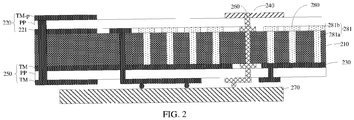
- the antenna packaging module includes an antenna substrate 210, a first laminated circuit 220, a ground layer 230, a radiator 240, a second laminated circuit 250, a feed structure 260, a radio frequency chip 270 and a conductive grid 280.
- the antenna substrate 210, the first laminated circuit 220, the ground layer 230, and the second laminated circuit 250 may be integrated in a multilayer printed circuit board (PCB) which is integrated by a high-density interconnect (HDI) process.
- the multilayer PCB may include a core layer, prepreg (PP) layers laminated respectively on two sides of the core layer, and metal layers TM plated on each PP layer and the core layer.
- the PP layer is a semi-cured sheet disposed between two copper layers. The two copper layers are attached to two opposite sides of the PP layer, respectively, and the two copper layers are insulated from each other.
- the metal layer TM can be a copper layer, a tin layer, a lead-tin alloy layer, a tin-copper alloy layer, etc.
- the antenna substrate 210 may be considered as the core layer.
- the antenna substrate 210 includes a first surface and a second surface opposite to the first surface.
- the first laminated circuit 220 is disposed on the first surface of the antenna substrate 210.
- the first laminated circuit 220 may include a number of spaced metal layers TM and PP layers, where the metal layer TM is arranged above the PP layer.
- the ground layer 230 is disposed on the second surface of the antenna substrate 210.
- the second laminated circuit 250 is disposed on a side of the ground layer 230 away from the antenna substrate 210. A side of the second laminated circuit 250 away from the ground layer 230 is configured to dispose a radio frequency chip 270.
- the second laminated circuit 250 may include a number of spaced metal layers TM and PP layers. The metal layer TM is arranged above the PP layer.
- a radiator 240 is disposed on a side of the first laminated circuit 220 away from the antenna substrate 210. Specifically, the radiator 240 is disposed on the top metal layer TM-p to receive and transmit millimeter wave signals. The radiator 240 is further provided with a feed point for feeding current signals. The feed point is connected to the radio frequency chip 270 via the feed structure 260.
- the radiator 240 may be a phased antenna array configured to radiate millimeter wave signals.
- the radiator 240 which is configured to radiate the millimeter wave signals, may be an antenna array formed by antennas selected from types of a patch antenna, a dipole antenna, a yagi antenna, a beam antenna, or other suitable antenna elements.
- the feed structure 260 extends through the second laminated circuit 250, the ground layer 230, the antenna substrate 210 and the first laminated circuit 220 to connect the radio frequency chip 270 and the radiator 240.
- the second laminated circuit 250, the ground layer 230, the antenna substrate 210 and the first laminated circuit 220 may define a number of through holes therein.
- a location of the through hole on the first laminated circuit 220 is set corresponding to a location of the feed point.
- Conductive material is filled in the through holes to form the feed structure 260, and the radio frequency chip 270 and the radiator 240 are conducted via the feed structure 260.
- the radio frequency chip 270 is connected to the radiator 240 via the feed structure 260 to feed current signals into the radiator 240, thereby receiving and transmitting the millimeter wave signals.
- the conductive grid 280 includes a number of spaced conductive structures 281, the conductive structures 281 extends through the antenna substrate 210 and connect to the ground layer 230. A portion of the feed structure 260 is disposed in a space formed by two adjacent conductive structures 281.
- material of the conductive structures 281 may be a conductive material, such as a metallic material, an alloy material, a conductive silicone material, a graphite material, etc.
- the material of the conductive structures 281 may be copper.
- the aforementioned antenna packaging module can suppress a surface wave, that is, the antenna packaging module has characteristics of high impedance for the surface wave in a certain frequency band.
- the antenna packaging module has a suppressive effect on the surface wave of a surface propagation frequency within an attenuation band, or cannot support propagation of the surface wave of a frequency band within the attenuation band, and then an antenna radiation efficiency is improved, thereby improving an antenna gain.
- the surface wave is a guided wave propagating along an interface between two media.
- a medium substrate of a plane antenna can restrict part of electromagnetic wave to propagate at the interface between medium and air.
- the introduced conductive grid 280 which can be considered as a number of parallel LC circuits, can improve the impedance bandwidth of the antenna and enhance isolation between ports of the antenna.
- size of the radiator 240 along a non-scanning direction can be reduced, thereby reducing a volume of the entire antenna packaging module.
- the first laminated circuit 220 includes a first conductive layer 221 adjacent to a side of the antenna substrate 210.
- the first conductive layer 221 can be considered as a metal layer TM disposed adjacent to the antenna substrate 210.
- the metal layer TM can be a copper layer, a tin layer, a lead-tin alloy layer, a tin-copper alloy layer, etc.
- the conductive structure 281 includes a conductive column 281a extending through the antenna substrate 210 and a conductive sheet 281b disposed on the first conductive layer 221.
- the conductive sheet 281b is connected to the ground layer 230 via the conductive column 281a.
- a shape of the conductive sheet 281b may include at least one of a rectangle (shown in FIG. 3a ), an annulus (shown in FIG. 3b ), a circle (shown in FIG. 3c ), an ellipse, a mushroom shape, an inverted "H" shape, and a cross shape.
- the shape of the conductive sheet 281b may be set according to an actual demand, and is not limited to the above examples.
- a size of the conductive sheet 281b is related to thickness and dielectric constant of the antenna substrate 210.
- the size of the conductive sheet 281b is not further limited.
- a resonant frequency of the radiator 240 can be adjusted by adjusting the sizes of the conductive sheets 281b, the thickness and the dielectric constant of the antenna substrate 210.
- the conductive columns 281a are in one-to-one correspondence with the conductive sheets 281b.
- the conductive structures 281 are electrically connected to an antenna layer via the conductive columns 281a.
- the antenna substrate 210 defines a number of through holes, and conductive material are filled in the through holes to form conductive columns 281a.
- the conductive columns 281a are in one-to-one correspondence with the conductive sheets 281b.
- the conductive structures 281 are electrically connected to the ground layer 230 via the conductive columns 281a to achieve a common ground for the conductive sheets 281b via the conductive columns 281a.
- the spaced conductive sheets 281b are respectively independent and not connected to each other, thereby achieving a mutual capacitive coupling between the conductive sheets 281b.
- a shape of a cross section of the conductive column 281a along a plane of the antenna substrate is the same as a shape of the conductive sheet 281b connected to the conductive column 281a. That is, the conductive column 281a may be considered as the conductive sheet 281b with greater thickness, and the thickness of the conductive column 281a is the thickness of the antenna substrate 210.
- the shape of the conductive sheet 281b is a circular
- the shape of the conductive column 281a connected to the conductive sheet 281b is a cylindrical.
- the material of the conductive columns 281a which is formed by filling the conductive material in the through hole, is the same as the material of the conductive structure 281.
- the material may be a metal material, a graphite material, etc.
- a number of the conductive sheets 281b are periodically arranged on a first conductive layer 221.
- the conductive sheets may be arranged as a honeycomb arrangement structure, a diamond arrangement structure, a rectangular arrangement structure, a radial arrangement structure, a gradient arrangement structure, etc.
- Each of the conductive sheets 281b in a conductive grid 280 may be same or different in shape.
- the periodically arranged conductive sheets 281b are rotationally symmetric or axially symmetric in a plane.
- each of the periodically arranged conductive sheets 281b in a plane is same in shape, and an area of each of the periodically arranged conductive sheets 281b is equal.
- the conductive sheets 281b in the conductive grid 280 are arranged in a two-dimensional array.
- each of the conductive sheets 281b in the conductive structure 281 is same in shape, an area of the conductive sheet 281b located at a center of the conductive grid 280 is the largest, and areas of the conductive sheets 281b decrease gradually along a direction radiating from the center to the periphery.
- the conductive sheets 281b in the conductive grid 280 are arranged in a two-dimensional rectangular array of M ⁇ M, the shape of each of the conductive sheets 281b in the conductive grid 280 is circular, a center-to-center distance between two adjacent conductive sheets 281b is equal, or an edge-to-edge distance between two adjacent conductive sheets 281b is equal.
- M may be 4, 5, 6 or an integer greater than 6. In the embodiments of the disclosure, the shape of the conductive sheet 281b, and the value of M are not further limited.
- the impedance bandwidth and gain of the antenna packaging module can be improved simultaneously, a beam width of a main lobe of the antenna packaging module can be diminished, and a directionality of the antenna packaging module can be enhanced.
- each of the conductive sheets 281b in the conductive grid 280 is same in shape, and areas of the conductive sheets 281b in each row of the conductive grid 280 gradually decreases along a direction.
- the conductive sheets 281b in the conductive grid 280 are arranged in a two-dimensional rectangular array of M ⁇ M, and the shape of each of the conductive sheets 281b is rectangular.
- the areas of the conductive sheets 281b gradually reduce along a row direction from the first row to the M-th row, or the areas of the conductive sheets 281b gradually enlarge along the row direction.
- a trend of enlarging areas of the two adjacent conductive sheets 281b along the row direction is the same, or a trend of reducing areas of the two adjacent conductive sheets 281b along the row direction is the same, that is, the areas are reduced in a same proportion or the areas are enlarged in a same proportion.
- the areas of the conductive sheets 281b gradually reduce along a column direction from the first column to the M-th column, or the areas of the conductive sheets 281b enlarge along the column direction.
- a trend of enlarging areas of the two adjacent conductive sheets 281b along the column direction is the same, or a trend of reducing areas of the two adjacent conductive sheets 281b along the column direction is the same, that is, the areas are reduced in a same proportion or the areas are enlarged in a same proportion.
- M may be 4, 5, 6 or an integer greater than 6.
- the shape of the conductive sheet 281b, and the value of M are not further limited.
- center-to-center distance can be considered as a distance between the respective centers of the two adjacent conductive sheets 281b
- edge-to-edge distance can be considered as the shortest distance between edges of the two adjacent conductive sheets 281b.
- the impedance bandwidth and gain of the antenna packaging module can be improved simultaneously, a beam width of a main lobe of the antenna packaging module is diminished, and a directionality of the antenna packaging module is enhanced.
- the center distance can be understood as the spacing between the respective centers of the two adjacent conductive sheets 281b; the edge distance can be understood as the shortest spacing between the edges of the two adjacent conductive sheets 281b.
- the impedance bandwidth and gain of the antenna packaging module can be improved simultaneously, a beam width of a main lobe of the antenna packaging module can be diminished, and a directionality of the antenna packaging module can be enhanced.
- an antenna packaging module provided in an embodiment includes an antenna substrate 210, a first laminated circuit 220, a ground layer 230, a radiator 240, a second laminated circuit 250, a feed structure 260, and a conductive grid 280.
- the antenna substrate 210, the first laminated circuit 220 and the second laminated circuit 250 are laminated by a PCB of 8-layer millimeter wave package antenna integrated by the High Density Interconnect (HDI) process.
- the first laminated circuit 220 includes metal layers TM1-TM4, and PP layers (including PP1 ⁇ PP3) between the adjacent metal layers.
- the metal layers TM1-TM4 are the copper layers of the antenna.
- the metal layer TM4 can be considered as a first conductive layer 221 of the first laminated circuit 220 which is adjacent to a side of the antenna substrate 210.
- the radiator 240 is arranged above the metal layer TM1.
- the metal layer TM5 is the ground layer 230.
- the second laminated circuit 250 includes metal layers TM6-TM8 and PP layers (including PP4 ⁇ PP6) between adjacent metal layer.
- the metal layers TM6-TM8 are copper layers of the wiring in a feed network and control lines the antenna package module, and the radio frequency chip 270 is soldered to the TM8.
- PP1-PP6 are semi-cured sheets disposed between two metal layer s TM (such as copper layers), each PP layer insulates and adheres the two adjacent metal layers.
- the conductive grid 280 (a number of periodically spaced conductive sheets 281b located at TM4 and a conductive column 281a extending through the antenna substrate 210) in the metal layer TM4 and the antenna substrate 210 to connect with TM5 (the ground layer 230) to form a ground layer of the radiator 240, surface waves can be suppressed, thereby improving the antenna radiation efficiency and the antenna gain.
- the introduced conductive grid 280 which can be considered a number of parallel LC circuits, can improve the impedance bandwidth of the antenna and enhance isolation between ports of the antenna.
- size of the radiator 240 along a non-scanning direction can be reduced, thereby reducing a volume of the entire antenna packaging module.
- an electronic device includes a housing and an antenna packaging module of any of the above embodiments, and the antenna packaging module is accommodated in the housing.
- the electronic device includes at least two of the antenna packaging modules which are disposed on different sides of the housing.
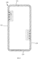
- the housing includes a first edge 121, a third edge 123 opposite to the first edge 121, a second edge 122, and a fourth edge 124 opposite to the second edge 122.
- the second edge 122 is connected to an end of the first edge 121 and an end of the third edge 123
- the fourth edge 124 is connected to the first edge 121 and the other end of the third edge 123.
- Millimeter wave modules are respectively disposed on at least two of the first edge 121, the second edge 122, the third edge 123 and the fourth edge 124.
- the two millimeter modules are respectively disposed on the second edge 122 and the fourth edge 124, thereby reducing an overall size of the antenna packaging module in the non-scanning direction and making it possible to place the antenna packaging module on both sides of the electronic device.
- the electronic device with the antenna packaging module of any of the above embodiments can be used to receive and transmit the millimeter wave signals for 5G communications, improve distortions of directional map and impedance bandwidth of the antenna packaging module, enhance the radiation efficiency and radiation gain of the millimeter wave signals, and reduce the space occupied by the antenna packaging module in the electronic device.
- the electronic device may include a mobile phone, a tablet computer, a notebook computer, a palmtop computer, a mobile internet device (MID), a wearable device (such as a smart watch, a smart bracelet, a pedometer, and so on) or other communication modules provided with an antenna.
- a mobile phone such as a smart phone, a tablet computer, a notebook computer, a palmtop computer, a mobile internet device (MID), a wearable device (such as a smart watch, a smart bracelet, a pedometer, and so on) or other communication modules provided with an antenna.
- MID mobile internet device
- a wearable device such as a smart watch, a smart bracelet, a pedometer, and so on
- FIG. 6 is a block diagram of a partial structure of a mobile phone related to an electronic device according to an embodiment of the present disclosure.
- the mobile phone 600 includes: an array antenna 610, a memory 620, an input unit 630, a display unit 640, a sensor 650, an audio circuit 660, a wireless fidelity (WIFI) module 670, a processor 680, a power supply 690 and other components.
- WIFI wireless fidelity
- FIG. 6 is not construed to limit the mobile phone, and may include more or less components than the components illustrated, or combine some components, or have different component arrangements.
- the array antenna 610 may be used for receiving and transmitting signals in the process of receiving and transmitting information or calling. After receiving a downlink information of a base station, the array antenna 610 may transmit the information to the processor 680, or, the array antenna 610 may transmit an uplink data to the base station.
- the memory 620 may be configured to store software programs and modules, and the processor 680 may perform various function applications and data processing of the mobile phone by running the software programs and modules stored in the memory 620.
- the memory 620 may mainly include a program memory area and a data memory area.
- the program memory area may store an operating system, an application program required for at least one function (such as an application program for sound playing function, an application program for image playing function).
- the data memory area may store data (such as audio data, address book, and so on) created according to the use of the mobile phone, and so on.
- the memory 620 may include a high-speed random access memory and may further include a non-volatile memory, such as at least one disk memory member, a flash memory member, or other volatile solid memory members.
- the input unit 630 may be used to receive input digital or character information, and generate a key signal input related to the user setting and the function control of the mobile phone 600.
- the input unit 630 may include a touch panel 631 and other input devices 632.
- the touch panel 631 also known as a touch screen, may collect user's touch operations on or near it (such as user's operations on or near the touch panel 631 with any suitable object or accessory such as a finger, a touch pen), and drive a corresponding connection device according to a preset program.
- the touch panel 631 may include two parts: a touch measuring device and a touch controller.
- the touch measuring device measures a touch orientation of the user, measures a signal brought by the touch operation, and transmits the signal to the touch controller.
- the touch controller receives touch information from the touch measuring device, converts it into a contact coordinate, then sends it to the processor 680, and receives and executes a command sent by the processor 680.
- various kinds of touch panels 631 may be realized, such as a resistance touch panel, a capacitance touch panel, an infrared touch panel and a surface-acoustic-wave touch panel.
- the input unit 630 may further include other input devices 632.
- the other input devices 632 may include, but are not limited to, one or more of a physical keyboard, and a function key (such as a volume control key, a switch key, and so on).
- the display unit 640 may be used to display information that is input by the user or provided to the user and various menus of the mobile phone.
- the display unit 640 may include a display panel 641.
- the display panel 641 may be configured in a form of a liquid crystal display (LCD), an organic light-emitting diode (OLED), and so on.
- the touch panel 631 may cover the display panel 641. When the touch panel 631 measures a touch operation on or near it, the touch operation is transmitted to the processor 680 to determine a type of the touch operation. Then, the processor 680 provides a corresponding visual output on the display panel 641 according to the type of touch operation.
- the touch panel 631 and the display panel 641 serve as two independent components to realize the input and input functions of the mobile phone, the touch panel 631 and the display panel 641 may be integrated to realize the input and output functions of the mobile phone in some embodiments.
- the mobile phone 600 may further include at least one sensor 650, such as an optical sensor, a motion sensor, and other sensors.
- the light sensor may include an ambient light sensor and a proximity sensor.
- the ambient light sensor may adjust a brightness of the display panel 641 according to the light and shade of an ambient light, and the proximity sensor may turn off the display panel 641 and/or the backlight when the mobile phone moves to an ear.
- the motion sensor may include an acceleration sensor, which may measure accelerations in all directions. When the motion sensor stays still, it may measure a magnitude and a direction of gravity, which may be used to applications identifying a mobile phone posture (such as a horizontal and vertical screen switching), and functions related to vibration identification (such as a pedometer, a percussion), and so on.
- the mobile phone may be provided with a gyroscope, a barometer, a hygrometer, a thermometer, an infrared sensor and other sensors.
- An audio circuit 660, a speaker 661 and a microphone 662 may provide an audio interface between the user and the mobile phone.
- the audio circuit 660 may transmit an electrical signal converted from the received audio data to the speaker 661, and the speaker 661 converts the electrical signal to a sound signal to be output.
- the microphone 662 converts a collected audio signal into an electrical signal
- the audio circuit 660 receives the electrical signal and converts the electrical signal into audio data
- the audio data is output to the processor 680 to be processed. Then, the processed audio date is sent to another mobile phone by the array antenna 610, or output to the memory 620 for subsequent processing.
- the processor 680 is a control center of the mobile phone, which uses various interfaces and lines to connect all parts of the mobile phone, and performs various functions of the mobile phone and processes data by running or executing software programs and/or modules stored in the memory 620 and invoking data stored in the memory 620, so as to overall monitor the mobile phone.
- the processor 680 may include one or more processing units.
- the processor 680 may integrate an application processor and a modulating-demodulating processor.
- the application processor mainly processes an operating system, a user interface, an application program, and so on.
- the modulating-demodulating processor mainly processes a wireless communication. It should be understood that the above modulating-demodulating processor may not be integrated into the processor 680.
- the mobile phone 600 further includes a power supply 690 (such as a battery) for supplying power to each component.
- a power supply 690 such as a battery
- the power supply may be logically connected to the processor 680 through a power management system, so as to realize functions of charging, discharging, and power consumption management through the power management system.
- the mobile phone 600 may further include a camera, a Bluetooth module, and so on.
- Any reference to a memory, a storage, a database or other media used in the disclosure may include a non-volatile and/or volatile memory.
- a suitable non-volatile memory may include a read-only memory (ROM), a programmable ROM (PROM), an electrically programmable ROM (EPROM), an electrically erasable programmable ROM (EEPROM), or a flash memory.
- the volatile memory may include a random access memory (RM), which is used as an external cache memory.
- the RM may be obtained in many forms, such as static random access memory (SRM), a dynamic random access memory (DRM), a synchronous dynamic random access memory (SDRM), a double data rate synchronous dynamic random access memory (DDR SDRM), an enhanced synchronous dynamic random access memory (ESDRM), a synchlink dynamic random access memory (SLDRM), a rambus direct random access memory (RDRM), a direct rambus dynamic random access memory (DRDRM), and a rambus dynamic random access memory (RDRM).
- SRM static random access memory
- DRM synchronous dynamic random access memory
- DDR SDRM double data rate synchronous dynamic random access memory
- EDRM enhanced synchronous dynamic random access memory
- SRM synchlink dynamic random access memory
- RDRM rambus direct random access memory
- DDRDRM direct rambus dynamic random access memory
- RDRM rambus dynamic random access memory
Landscapes
- Engineering & Computer Science (AREA)
- Computer Networks & Wireless Communication (AREA)
- Physics & Mathematics (AREA)
- Optics & Photonics (AREA)
- Microelectronics & Electronic Packaging (AREA)
- Support Of Aerials (AREA)
- Variable-Direction Aerials And Aerial Arrays (AREA)
- Details Of Aerials (AREA)
Abstract
Description
- This application claims priority to a
CN application No.2019102114118 filed on March 20, 2019 - The disclosure relates to the technical field of antenna, and more particularly, to an antenna device and electronic device.
- Provided here is background information relevant to the disclosure and does not necessarily constitutes the exemplary prior art.
- With the development of wireless communication technology, technology of 5G network has emerged. As the fifth-generation mobile communication network, 5G network has a theoretical peak transmission speed up to tens of Gb per second, which is hundreds of times faster than the transmission speed of 4G network. Therefore, millimeter wave band with sufficient spectrum resources has become one of operating bands for 5G communication system.
- Millimeter-wave packaging antenna module is a mainstream packaging solution for future 5G millimeter wave electronic devices. The millimeter wave packaging antenna module can adopt a high-density interconnection process of a multilayer PCB and dispose a radiator on a side of the module. However, the radiator generally takes a microstrip patch antenna array. A size of the microstrip patch antenna array is mainly limited by a dielectric constant of the multilayer PCB board, and radiation efficiency of the microstrip patch antenna array is relatively low.
- The disclosure provides an antenna device and an electronic device, according to various embodiments.
- An antenna packaging module includes: an antenna substrate, a radiator, a second laminated circuit, a feed structure, and a conductive grid. A first laminated circuit and a ground layer are disposed respectively on two opposite sides of the antenna substrate. The radiator is disposed on a side of the first laminated circuit away from the antenna substrate. The second laminated circuit is disposed on a side of the ground layer away from the antenna substrate, and a side of the second laminated circuit away from the ground layer is configured to dispose a radio frequency chip. A feed structure extends through the second laminated circuit, the ground layer, the antenna substrate and the first laminated circuit, the feed structure is configured to connect the radio frequency chip and the radiator. The conductive grid includes a number of spaced conductive structures, the conductive structures extend through the antenna substrate and are connected with the ground layer, and a portion of the feed structure is disposed in a space formed by two adjacent conductive structures.
- An electronic device is further provided. The electronic device includes a housing and the above-mentioned antenna packaging module. The antenna packaging module is accommodated in the housing.
- The antenna packaging module and the electronic device includes: an antenna substrate, a radiator, a second laminated circuit, a feed structure, and a conductive grid. A first laminated circuit and a ground layer are disposed respectively on two opposite sides of the antenna substrate. The radiator is disposed on a side of the first laminated circuit away from the antenna substrate. The second laminated circuit is disposed on a side of the ground layer away from the antenna substrate, and a side of the second laminated circuit away from the ground layer is configured to dispose a radio frequency chip. The feed structure extends through the second laminated circuit, the ground layer, the antenna substrate and the first laminated circuit, the feed structure is configured to connect the radio frequency chip and the radiator. The conductive grid includes a number of spaced conductive structures, the conductive structures extend through the antenna substrate and are connected with the ground layer, and a portion of the feed structure is disposed in a space formed by two adjacent conductive structures. By introducing the conductive grid, surface wave can be suppressed, and the antenna radiation efficiency and antenna gain can be improved.
- Details of one or more embodiments of the disclosure will be described in the following drawings and description. Other features, objects and advantages of the disclosure will become more apparent from the description, the drawings, and the claims.
- In order to more clearly illustrate the embodiments of the present disclosure or related art, the following figures will be described in the embodiments are briefly introduced. It is obvious that the drawings are merely some embodiments of the present disclosure, and other drawings can also be obtained by those skilled in the art according to these drawings without any creative effort.
-
FIG. 1 is a stereo diagram of an electronic device according to an embodiment of the disclosure; -
FIG. 2 is a schematic structural diagram of an antenna packaging module according to an embodiment of the disclosure; -
FIG. 3a is a schematic diagram showing the structure of conductive sheets, according to an embodiment of the disclosure; -
FIG. 3b is a schematic diagram showing the structure of conductive sheets, according to another embodiment of the disclosure; -
FIG. 3c is a schematic diagram showing the structure of conductive sheets, according to still another embodiment of the disclosure; -
FIG. 4 is a schematic structural diagram of an antenna packaging module according to another embodiment of the disclosure; -
FIG. 5 is a main view of a housing according to another embodiment of the disclosure, wherein the housing is included in the electronic device illustrated inFIG. 1 ; and -
FIG. 6 is a block diagram showing partial structure of a mobile phone, which is relevant to the electronic device provided in the embodiments of the disclosure. - In order to more clearly and obviously illustrate objects, technical solutions and advantages of the disclosure, the disclosure will be further described in detail below with reference to the accompanying drawings and embodiments. It should be understood that the specific embodiments described herein are merely used to explain the disclosure, but not to limit the disclosure.
- It should be understood that terms such as "first", "second", etc. are used herein for describing various elements, but these elements should not be limited by these terms. These terms are only used for distinguishing one element from another element, and are not intended to indicate or imply relative importance or to imply the number of indicated technical features. Thus, the feature defined with "first" and "second" may explicitly or implicitly include at least one such feature. In the description of the disclosure, "a number of' means two or more than two, such as two and three, unless expressly specified otherwise.
- It should be noted that when an element is described to be arranged to another element, the element may be directly arranged on another component or there may be an intermediate element. When an element is considered to be connected to another element, the element may be directly connected to another component or there may be an intermediate element.
- An antenna module according to an embodiment of the disclosure is applied to an electronic device. In an embodiment, the electronic device may include a mobile phone, a tablet computer, a notebook computer, a palmtop computer, a mobile Internet device (MID), a wearable device (such as a smart watch, a smart bracelet, a pedometer, etc.) or other communication modules provided with an array antenna module.
- As illustrated in
FIG. 1 , anelectronic device 10 provided in an embodiment of the disclosure may include adisplay assembly 110, ahousing assembly 120 and a controller. Thedisplay assembly 110 is fixed to thehousing assembly 120 and forms an external structure of the electronic device together with thehousing assembly 120. Thehousing assembly 120 may include a middle frame and a rear cover. The middle frame may be a frame structure having a through hole. The middle frame may be accommodated in an accommodating space formed by the display assembly and the rear cover. The rear cover is used to form an external profile of the electronic device. The rear cover may be formed integrally. In a molding process of the rear cover, a rear camera hole, a fingerprint identification module, an antenna module mounting hole and other structures may be formed in the rear cover. The rear cover may be a non-metallic rear cover. For example, the rear cover may be a plastic rear cover, a ceramic rear cover, a 3D glass rear cover, and so on. The controller is configured to control an operation of the electronic device. The display assembly may be used to display pictures or texts, and may provide a user with an operation interface. - In an embodiment, the
housing assembly 120 is integrated with an antenna packaging module. The antenna packaging module can transmit and receive millimeter wave signals through thehousing assembly 120, such that the electronic device may achieve a wide coverage of the millimeter wave signals. - The millimeter wave refers to an electromagnetic wave with a millimeter-level wavelength, and a frequency of the millimeter wave is approximately between 20 GHz and 300 GHz. The 3rd Generation Partnership Project (3GPP) has specified a list of frequency bands supported by 5G New Radio (NR), and spectrum range of 5G NR is up to 100GHz. 5G NR supports two major frequency bands: frequency range 1 (FR1), i.e., a sub 6 GHz frequency band, and frequency range 2 (FR2), i.e., a millimeter wave frequency band. The frequency range of FR1 frequency band is 450 MHz - 6 GHz, and the maximum channel bandwidth is 100MHz. The frequency range of FR2 is 24.25 GHz - 52.6 GHz, and the maximum channel bandwidth is 400MHz. A nearly 11GHz spectrum used for 5G mobile broadband includes: 3.85GHz licensed spectrum, such as: 28 GHz (24.25-29.5 GHz), 37GHz (37.0-38.6 GHz), 39 GHz (38.6-40 GHz) and 14 GHz unlicensed spectrum (57-71 GHz). 5G communication system operates in three bands as follows: 28 GHz, 39 GHz, and 60 GHz.
- As illustrated in
FIG. 2 , an embodiment of the disclosure provides an antenna packaging module. The antenna packaging module includes anantenna substrate 210, a firstlaminated circuit 220, aground layer 230, aradiator 240, a secondlaminated circuit 250, afeed structure 260, aradio frequency chip 270 and aconductive grid 280. - In an embodiment, the
antenna substrate 210, the firstlaminated circuit 220, theground layer 230, and the secondlaminated circuit 250 may be integrated in a multilayer printed circuit board (PCB) which is integrated by a high-density interconnect (HDI) process. The multilayer PCB may include a core layer, prepreg (PP) layers laminated respectively on two sides of the core layer, and metal layers TM plated on each PP layer and the core layer. The PP layer is a semi-cured sheet disposed between two copper layers. The two copper layers are attached to two opposite sides of the PP layer, respectively, and the two copper layers are insulated from each other. The metal layer TM can be a copper layer, a tin layer, a lead-tin alloy layer, a tin-copper alloy layer, etc. - In an embodiment, the
antenna substrate 210 may be considered as the core layer. Theantenna substrate 210 includes a first surface and a second surface opposite to the first surface. The firstlaminated circuit 220 is disposed on the first surface of theantenna substrate 210. In other embodiments, the firstlaminated circuit 220 may include a number of spaced metal layers TM and PP layers, where the metal layer TM is arranged above the PP layer. - In an embodiment, the
ground layer 230 is disposed on the second surface of theantenna substrate 210. - In an embodiment, the second
laminated circuit 250 is disposed on a side of theground layer 230 away from theantenna substrate 210. A side of the secondlaminated circuit 250 away from theground layer 230 is configured to dispose aradio frequency chip 270. In other embodiments, the secondlaminated circuit 250 may include a number of spaced metal layers TM and PP layers. The metal layer TM is arranged above the PP layer. - In an embodiment, a
radiator 240 is disposed on a side of the firstlaminated circuit 220 away from theantenna substrate 210. Specifically, theradiator 240 is disposed on the top metal layer TM-p to receive and transmit millimeter wave signals. Theradiator 240 is further provided with a feed point for feeding current signals. The feed point is connected to theradio frequency chip 270 via thefeed structure 260. - In an embodiment, the
radiator 240 may be a phased antenna array configured to radiate millimeter wave signals. For example, theradiator 240, which is configured to radiate the millimeter wave signals, may be an antenna array formed by antennas selected from types of a patch antenna, a dipole antenna, a yagi antenna, a beam antenna, or other suitable antenna elements. - The
feed structure 260 extends through the secondlaminated circuit 250, theground layer 230, theantenna substrate 210 and the firstlaminated circuit 220 to connect theradio frequency chip 270 and theradiator 240. - In an embodiment, the second
laminated circuit 250, theground layer 230, theantenna substrate 210 and the firstlaminated circuit 220 may define a number of through holes therein. A location of the through hole on the firstlaminated circuit 220 is set corresponding to a location of the feed point. Conductive material is filled in the through holes to form thefeed structure 260, and theradio frequency chip 270 and theradiator 240 are conducted via thefeed structure 260. Theradio frequency chip 270 is connected to theradiator 240 via thefeed structure 260 to feed current signals into theradiator 240, thereby receiving and transmitting the millimeter wave signals. - The
conductive grid 280 includes a number of spacedconductive structures 281, theconductive structures 281 extends through theantenna substrate 210 and connect to theground layer 230. A portion of thefeed structure 260 is disposed in a space formed by two adjacentconductive structures 281. - In an embodiment, material of the
conductive structures 281 may be a conductive material, such as a metallic material, an alloy material, a conductive silicone material, a graphite material, etc. In this embodiment, the material of theconductive structures 281 may be copper. - By introducing the
conductive grid 280 in theantenna substrate 210, the aforementioned antenna packaging module can suppress a surface wave, that is, the antenna packaging module has characteristics of high impedance for the surface wave in a certain frequency band. Specifically, the antenna packaging module has a suppressive effect on the surface wave of a surface propagation frequency within an attenuation band, or cannot support propagation of the surface wave of a frequency band within the attenuation band, and then an antenna radiation efficiency is improved, thereby improving an antenna gain. The surface wave is a guided wave propagating along an interface between two media. A medium substrate of a plane antenna can restrict part of electromagnetic wave to propagate at the interface between medium and air. Meanwhile, the introducedconductive grid 280, which can be considered as a number of parallel LC circuits, can improve the impedance bandwidth of the antenna and enhance isolation between ports of the antenna. By introducing theconductive grid 280, size of theradiator 240 along a non-scanning direction can be reduced, thereby reducing a volume of the entire antenna packaging module. - In an embodiment, the first
laminated circuit 220 includes a firstconductive layer 221 adjacent to a side of theantenna substrate 210. The firstconductive layer 221 can be considered as a metal layer TM disposed adjacent to theantenna substrate 210. The metal layer TM can be a copper layer, a tin layer, a lead-tin alloy layer, a tin-copper alloy layer, etc. - Specifically, the
conductive structure 281 includes aconductive column 281a extending through theantenna substrate 210 and aconductive sheet 281b disposed on the firstconductive layer 221. Theconductive sheet 281b is connected to theground layer 230 via theconductive column 281a. - As illustrated in
FIG. 3a, FIG. 3b andFIG. 3c , a shape of theconductive sheet 281b may include at least one of a rectangle (shown inFIG. 3a ), an annulus (shown inFIG. 3b ), a circle (shown inFIG. 3c ), an ellipse, a mushroom shape, an inverted "H" shape, and a cross shape. In the embodiments of the disclosure, the shape of theconductive sheet 281b may be set according to an actual demand, and is not limited to the above examples. - It should be noted that a size of the
conductive sheet 281b is related to thickness and dielectric constant of theantenna substrate 210. In the embodiments of the disclosure, the size of theconductive sheet 281b is not further limited. A resonant frequency of theradiator 240 can be adjusted by adjusting the sizes of theconductive sheets 281b, the thickness and the dielectric constant of theantenna substrate 210. - In an embodiment, the
conductive columns 281a are in one-to-one correspondence with theconductive sheets 281b. Theconductive structures 281 are electrically connected to an antenna layer via theconductive columns 281a. Specifically, theantenna substrate 210 defines a number of through holes, and conductive material are filled in the through holes to formconductive columns 281a. Theconductive columns 281a are in one-to-one correspondence with theconductive sheets 281b. Theconductive structures 281 are electrically connected to theground layer 230 via theconductive columns 281a to achieve a common ground for theconductive sheets 281b via theconductive columns 281a. Meanwhile, the spacedconductive sheets 281b are respectively independent and not connected to each other, thereby achieving a mutual capacitive coupling between theconductive sheets 281b. - In an embodiment, a shape of a cross section of the
conductive column 281a along a plane of the antenna substrate is the same as a shape of theconductive sheet 281b connected to theconductive column 281a. That is, theconductive column 281a may be considered as theconductive sheet 281b with greater thickness, and the thickness of theconductive column 281a is the thickness of theantenna substrate 210. For example, in a condition that the shape of theconductive sheet 281b is a circular, the shape of theconductive column 281a connected to theconductive sheet 281b is a cylindrical. The material of theconductive columns 281a, which is formed by filling the conductive material in the through hole, is the same as the material of theconductive structure 281. For example, the material may be a metal material, a graphite material, etc. - In an embodiment, a number of the
conductive sheets 281b are periodically arranged on a firstconductive layer 221. For example, the conductive sheets may be arranged as a honeycomb arrangement structure, a diamond arrangement structure, a rectangular arrangement structure, a radial arrangement structure, a gradient arrangement structure, etc. Each of theconductive sheets 281b in aconductive grid 280 may be same or different in shape. For example, the periodically arrangedconductive sheets 281b are rotationally symmetric or axially symmetric in a plane. - In an embodiment according to
FIG. 3a , each of the periodically arrangedconductive sheets 281b in a plane is same in shape, and an area of each of the periodically arrangedconductive sheets 281b is equal. For example, theconductive sheets 281b in theconductive grid 280 are arranged in a two-dimensional array. - In an embodiment, each of the
conductive sheets 281b in theconductive structure 281 is same in shape, an area of theconductive sheet 281b located at a center of theconductive grid 280 is the largest, and areas of theconductive sheets 281b decrease gradually along a direction radiating from the center to the periphery. For example, theconductive sheets 281b in theconductive grid 280 are arranged in a two-dimensional rectangular array of M∗M, the shape of each of theconductive sheets 281b in theconductive grid 280 is circular, a center-to-center distance between two adjacentconductive sheets 281b is equal, or an edge-to-edge distance between two adjacentconductive sheets 281b is equal. M may be 4, 5, 6 or an integer greater than 6. In the embodiments of the disclosure, the shape of theconductive sheet 281b, and the value of M are not further limited. - In this embodiment, by arranging the
conductive grid 280 in a two-dimensional rectangular array of M∗M where theconductive sheets 281b gradually change in two dimensions, the impedance bandwidth and gain of the antenna packaging module can be improved simultaneously, a beam width of a main lobe of the antenna packaging module can be diminished, and a directionality of the antenna packaging module can be enhanced. - In an embodiment, each of the
conductive sheets 281b in theconductive grid 280 is same in shape, and areas of theconductive sheets 281b in each row of theconductive grid 280 gradually decreases along a direction. For example, theconductive sheets 281b in theconductive grid 280 are arranged in a two-dimensional rectangular array of M∗M, and the shape of each of theconductive sheets 281b is rectangular. In the two-dimensional rectangular array of M∗M provided in an embodiment, the areas of theconductive sheets 281b gradually reduce along a row direction from the first row to the M-th row, or the areas of theconductive sheets 281b gradually enlarge along the row direction. A trend of enlarging areas of the two adjacentconductive sheets 281b along the row direction is the same, or a trend of reducing areas of the two adjacentconductive sheets 281b along the row direction is the same, that is, the areas are reduced in a same proportion or the areas are enlarged in a same proportion. - In a two-dimensional rectangular array of M∗M provided in another embodiment, the areas of the
conductive sheets 281b gradually reduce along a column direction from the first column to the M-th column, or the areas of theconductive sheets 281b enlarge along the column direction. A trend of enlarging areas of the two adjacentconductive sheets 281b along the column direction is the same, or a trend of reducing areas of the two adjacentconductive sheets 281b along the column direction is the same, that is, the areas are reduced in a same proportion or the areas are enlarged in a same proportion. - Further, in the two-dimensional rectangular array of M∗M, a center-to-center distance between two adjacent conductive sheets is equal, or an edge-to-edge distance between two adjacent conductive sheets is equal. M may be 4, 5, 6 or an integer greater than 6. In the embodiments of the disclosure, the shape of the
conductive sheet 281b, and the value of M are not further limited. - It should be noted that the center-to-center distance can be considered as a distance between the respective centers of the two adjacent
conductive sheets 281b, and the edge-to-edge distance can be considered as the shortest distance between edges of the two adjacentconductive sheets 281b. - In the embodiment, by arranging the
conductive grid 280 in a two-dimensional rectangular array of M∗M where theconductive sheets 281b gradually change in two dimensions, the impedance bandwidth and gain of the antenna packaging module can be improved simultaneously, a beam width of a main lobe of the antenna packaging module is diminished, and a directionality of the antenna packaging module is enhanced. - The center distance can be understood as the spacing between the respective centers of the two adjacent
conductive sheets 281b; the edge distance can be understood as the shortest spacing between the edges of the two adjacentconductive sheets 281b. - In this embodiment, by arranging the
conductive grid 280 in a two-dimensional rectangular array of M∗M where theconductive sheets 281b gradually change in two dimensions, the impedance bandwidth and gain of the antenna packaging module can be improved simultaneously, a beam width of a main lobe of the antenna packaging module can be diminished, and a directionality of the antenna packaging module can be enhanced. - As illustrated in
FIG. 4 , an antenna packaging module provided in an embodiment includes anantenna substrate 210, a firstlaminated circuit 220, aground layer 230, aradiator 240, a secondlaminated circuit 250, afeed structure 260, and aconductive grid 280. Theantenna substrate 210, the firstlaminated circuit 220 and the secondlaminated circuit 250 are laminated by a PCB of 8-layer millimeter wave package antenna integrated by the High Density Interconnect (HDI) process. The firstlaminated circuit 220 includes metal layers TM1-TM4, and PP layers (including PP1~ PP3) between the adjacent metal layers. The metal layers TM1-TM4 are the copper layers of the antenna. The metal layer TM4 can be considered as a firstconductive layer 221 of the firstlaminated circuit 220 which is adjacent to a side of theantenna substrate 210. - The
radiator 240 is arranged above the metal layer TM1. - The metal layer TM5 is the
ground layer 230. - The second
laminated circuit 250 includes metal layers TM6-TM8 and PP layers (including PP4~ PP6) between adjacent metal layer. The metal layers TM6-TM8 are copper layers of the wiring in a feed network and control lines the antenna package module, and theradio frequency chip 270 is soldered to the TM8. - It should be noted that PP1-PP6 are semi-cured sheets disposed between two metal layer s TM (such as copper layers), each PP layer insulates and adheres the two adjacent metal layers.
- By introducing the conductive grid 280 (a number of periodically spaced
conductive sheets 281b located at TM4 and aconductive column 281a extending through the antenna substrate 210) in the metal layer TM4 and theantenna substrate 210 to connect with TM5 (the ground layer 230) to form a ground layer of theradiator 240, surface waves can be suppressed, thereby improving the antenna radiation efficiency and the antenna gain. Meanwhile, the introducedconductive grid 280, which can be considered a number of parallel LC circuits, can improve the impedance bandwidth of the antenna and enhance isolation between ports of the antenna. By introducing theconductive grid 280, size of theradiator 240 along a non-scanning direction can be reduced, thereby reducing a volume of the entire antenna packaging module. - As illustrated in
FIG. 5 , an electronic device includes a housing and an antenna packaging module of any of the above embodiments, and the antenna packaging module is accommodated in the housing. - In an embodiment, the electronic device includes at least two of the antenna packaging modules which are disposed on different sides of the housing. For example, the housing includes a
first edge 121, athird edge 123 opposite to thefirst edge 121, asecond edge 122, and afourth edge 124 opposite to thesecond edge 122. Thesecond edge 122 is connected to an end of thefirst edge 121 and an end of thethird edge 123, and thefourth edge 124 is connected to thefirst edge 121 and the other end of thethird edge 123. Millimeter wave modules are respectively disposed on at least two of thefirst edge 121, thesecond edge 122, thethird edge 123 and thefourth edge 124. In a condition that there are two millimeter wave modules, the two millimeter modules are respectively disposed on thesecond edge 122 and thefourth edge 124, thereby reducing an overall size of the antenna packaging module in the non-scanning direction and making it possible to place the antenna packaging module on both sides of the electronic device. - The electronic device with the antenna packaging module of any of the above embodiments can be used to receive and transmit the millimeter wave signals for 5G communications, improve distortions of directional map and impedance bandwidth of the antenna packaging module, enhance the radiation efficiency and radiation gain of the millimeter wave signals, and reduce the space occupied by the antenna packaging module in the electronic device.
- The electronic device may include a mobile phone, a tablet computer, a notebook computer, a palmtop computer, a mobile internet device (MID), a wearable device (such as a smart watch, a smart bracelet, a pedometer, and so on) or other communication modules provided with an antenna.
-
FIG. 6 is a block diagram of a partial structure of a mobile phone related to an electronic device according to an embodiment of the present disclosure. As illustrated inFIG. 6 , themobile phone 600 includes: anarray antenna 610, amemory 620, aninput unit 630, adisplay unit 640, asensor 650, anaudio circuit 660, a wireless fidelity (WIFI)module 670, aprocessor 680, apower supply 690 and other components. It should be understood by those skilled in related art that the structure of the mobile phone illustrated inFIG. 6 is not construed to limit the mobile phone, and may include more or less components than the components illustrated, or combine some components, or have different component arrangements. - The
array antenna 610 may be used for receiving and transmitting signals in the process of receiving and transmitting information or calling. After receiving a downlink information of a base station, thearray antenna 610 may transmit the information to theprocessor 680, or, thearray antenna 610 may transmit an uplink data to the base station. Thememory 620 may be configured to store software programs and modules, and theprocessor 680 may perform various function applications and data processing of the mobile phone by running the software programs and modules stored in thememory 620. Thememory 620 may mainly include a program memory area and a data memory area. The program memory area may store an operating system, an application program required for at least one function (such as an application program for sound playing function, an application program for image playing function). The data memory area may store data (such as audio data, address book, and so on) created according to the use of the mobile phone, and so on. In addition, thememory 620 may include a high-speed random access memory and may further include a non-volatile memory, such as at least one disk memory member, a flash memory member, or other volatile solid memory members. - The
input unit 630 may be used to receive input digital or character information, and generate a key signal input related to the user setting and the function control of themobile phone 600. In an embodiment, theinput unit 630 may include atouch panel 631 andother input devices 632. Thetouch panel 631 also known as a touch screen, may collect user's touch operations on or near it (such as user's operations on or near thetouch panel 631 with any suitable object or accessory such as a finger, a touch pen), and drive a corresponding connection device according to a preset program. In an embodiment, thetouch panel 631 may include two parts: a touch measuring device and a touch controller. The touch measuring device measures a touch orientation of the user, measures a signal brought by the touch operation, and transmits the signal to the touch controller. The touch controller receives touch information from the touch measuring device, converts it into a contact coordinate, then sends it to theprocessor 680, and receives and executes a command sent by theprocessor 680. In addition, various kinds oftouch panels 631 may be realized, such as a resistance touch panel, a capacitance touch panel, an infrared touch panel and a surface-acoustic-wave touch panel. Besides thetouch panel 631, theinput unit 630 may further includeother input devices 632. In an embodiment, theother input devices 632 may include, but are not limited to, one or more of a physical keyboard, and a function key (such as a volume control key, a switch key, and so on). - The
display unit 640 may be used to display information that is input by the user or provided to the user and various menus of the mobile phone. Thedisplay unit 640 may include adisplay panel 641. In an embodiment, thedisplay panel 641 may be configured in a form of a liquid crystal display (LCD), an organic light-emitting diode (OLED), and so on. In an embodiment, thetouch panel 631 may cover thedisplay panel 641. When thetouch panel 631 measures a touch operation on or near it, the touch operation is transmitted to theprocessor 680 to determine a type of the touch operation. Then, theprocessor 680 provides a corresponding visual output on thedisplay panel 641 according to the type of touch operation. Although inFIG. 6 , thetouch panel 631 and thedisplay panel 641 serve as two independent components to realize the input and input functions of the mobile phone, thetouch panel 631 and thedisplay panel 641 may be integrated to realize the input and output functions of the mobile phone in some embodiments. - The
mobile phone 600 may further include at least onesensor 650, such as an optical sensor, a motion sensor, and other sensors. In an embodiment, the light sensor may include an ambient light sensor and a proximity sensor. The ambient light sensor may adjust a brightness of thedisplay panel 641 according to the light and shade of an ambient light, and the proximity sensor may turn off thedisplay panel 641 and/or the backlight when the mobile phone moves to an ear. The motion sensor may include an acceleration sensor, which may measure accelerations in all directions. When the motion sensor stays still, it may measure a magnitude and a direction of gravity, which may be used to applications identifying a mobile phone posture (such as a horizontal and vertical screen switching), and functions related to vibration identification (such as a pedometer, a percussion), and so on. In addition, the mobile phone may be provided with a gyroscope, a barometer, a hygrometer, a thermometer, an infrared sensor and other sensors. - An
audio circuit 660, aspeaker 661 and amicrophone 662 may provide an audio interface between the user and the mobile phone. Theaudio circuit 660 may transmit an electrical signal converted from the received audio data to thespeaker 661, and thespeaker 661 converts the electrical signal to a sound signal to be output. On the other hand, themicrophone 662 converts a collected audio signal into an electrical signal, theaudio circuit 660 receives the electrical signal and converts the electrical signal into audio data, and the audio data is output to theprocessor 680 to be processed. Then, the processed audio date is sent to another mobile phone by thearray antenna 610, or output to thememory 620 for subsequent processing. - The
processor 680 is a control center of the mobile phone, which uses various interfaces and lines to connect all parts of the mobile phone, and performs various functions of the mobile phone and processes data by running or executing software programs and/or modules stored in thememory 620 and invoking data stored in thememory 620, so as to overall monitor the mobile phone. In an embodiment, theprocessor 680 may include one or more processing units. In an embodiment, theprocessor 680 may integrate an application processor and a modulating-demodulating processor. The application processor mainly processes an operating system, a user interface, an application program, and so on. The modulating-demodulating processor mainly processes a wireless communication. It should be understood that the above modulating-demodulating processor may not be integrated into theprocessor 680. - The
mobile phone 600 further includes a power supply 690 (such as a battery) for supplying power to each component. In some embodiments, the power supply may be logically connected to theprocessor 680 through a power management system, so as to realize functions of charging, discharging, and power consumption management through the power management system. - In an embodiment, the
mobile phone 600 may further include a camera, a Bluetooth module, and so on. - Any reference to a memory, a storage, a database or other media used in the disclosure may include a non-volatile and/or volatile memory. A suitable non-volatile memory may include a read-only memory (ROM), a programmable ROM (PROM), an electrically programmable ROM (EPROM), an electrically erasable programmable ROM (EEPROM), or a flash memory. The volatile memory may include a random access memory (RM), which is used as an external cache memory. The RM may be obtained in many forms, such as static random access memory (SRM), a dynamic random access memory (DRM), a synchronous dynamic random access memory (SDRM), a double data rate synchronous dynamic random access memory (DDR SDRM), an enhanced synchronous dynamic random access memory (ESDRM), a synchlink dynamic random access memory (SLDRM), a rambus direct random access memory (RDRM), a direct rambus dynamic random access memory (DRDRM), and a rambus dynamic random access memory (RDRM).
- Respective technical features of the above embodiments may be combined arbitrarily. In order to make the description concise, not all possible combinations of the respective technical features in the above embodiments have been described. However, as long as the combinations of these technical features do not have contradictions, they should be considered to be fallen into the scope of the description.
- The above embodiments only illustrate several implementations of the disclosure, and the descriptions thereof are specific and detailed, but it cannot not be understood as limiting the protection scope of the disclosure. It should be noted that, for those skilled in the related art, several modifications and variants can be made without departing from the principle of the disclosure, which belong to the protection scope of the present disclosure. Therefore, the protection scope of the patent of the disclosure shall be subject to the appended claims.
Claims (20)
- An antenna packaging module, comprising:an antenna substrate, a first laminated circuit and a ground layer being disposed respectively on two opposite sides of the antenna substrate;a radiator disposed on a side of the first laminated circuit away from the antenna substrate;a second laminated circuit disposed on a side of the ground layer away from the antenna substrate, a side of the second laminated circuit away from the ground layer being configured to dispose a radio frequency chip;a feed structure extending through the second laminated circuit, the ground layer, the antenna substrate and the first laminated circuit, the feed structure being configured to connect the radio frequency chip and the radiator; anda conductive grid comprising a plurality of spaced conductive structures, the conductive structures extending through the antenna substrate and being connected with the ground layer, and a portion of the feed structure being disposed in a space formed by two adjacent conductive structures.
- The antenna packaging module as claimed in claim 1, wherein the first laminated circuit comprises a first conductive layer adjacent to a side of the antenna substrate.
- The antenna packaging module as claimed in claim 2, wherein the conductive structure comprises a conductive column extending through the antenna substrate and a conductive sheet disposed on the first conductive layer, and the conductive sheet is connected to the ground layer via the conductive column.
- The antenna packaging module as claimed in claim 1, wherein a plurality of conductive sheets are periodically arranged on a first conductive layer.
- The antenna packaging module as claimed in claim 4, wherein the periodically arranged conductive sheets are rotationally symmetric in a plane.
- The antenna packaging module as claimed in claim 4, wherein the periodically arranged conductive sheets are axially symmetric in a plane.
- The antenna packaging module as claimed in claim 5 or claim 6, wherein the periodically arranged conductive sheets are same in shape, an area of the conductive sheet located at a center of the conductive grid is the largest, and areas of the conductive sheets decrease gradually along a direction from the center to the periphery.
- The antenna packaging module as claimed in claim 5 or claim 6, wherein areas of the periodically arranged conductive sheets in each row decrease along a same direction, or areas of the periodically arranged conductive sheets in each row increase along a same direction.
- The antenna packaging module as claimed in claim 5 or claim 6, wherein an area of each of the periodically arranged conductive sheets is equal.
- The antenna packaging module as claimed in claim 1, wherein a center-to-center distance between two adjacent conductive sheets is equal, or an edge-to-edge distance between two adjacent conductive sheets is equal.
- The antenna packaging module as claimed in claim 1, wherein a shape of a cross section of a conductive column along a plane of the antenna substrate is the same as a shape of a conductive sheet connected to the conductive column.
- The antenna packaging module as claimed in claim 1, wherein a shape of a conductive sheet comprising at least one of a rectangle, an annulus, a circle, an ellipse, a mushroom shape and an inverted "H" shape.
- The antenna package module as claimed in claim 1, wherein the second laminated circuit, the ground layer, the antenna substrate and the first laminated circuit define a plurality of through holes therein, and conductive material are filled in the through holes to form the feed structure.
- The antenna package module as claimed in claim 1 wherein the radiator is an antenna array formed by antennas selected from at least one type of a patch antenna, a dipole antenna and a yagi antenna.
- An electronic device, comprising:a housing; andan antenna packaging module accommodated in the housing, wherein the antenna packaging module comprises:an antenna substrate, a first laminated circuit and a ground layer being disposed respectively on two opposite sides of the antenna substrate;a radiator disposed on a side of the first laminated circuit away from the antenna substrate;a second laminated circuit disposed on a side of the ground layer away from the antenna substrate, a side of the second laminated circuit away from the ground layer being configured to dispose a radio frequency chip;a feed structure extending through the second laminated circuit, the ground layer, the antenna substrate and the first laminated circuit, the feed structure being configured to connect the radio frequency chip and the radiator; anda conductive grid comprising a plurality of spaced conductive structures, the conductive structures extending through the antenna substrate and being connected with the ground layer, and a portion of the feed structure being disposed in a space formed by two adjacent conductive structures.
- The electronic device as claimed in claim 15, wherein the first laminated circuit comprises a first conductive layer adjacent to a side of the antenna substrate.
- The electronic device as claimed in claim 16, wherein the conductive structure comprises a conductive column extending through the antenna substrate and a conductive sheet disposed on the first conductive layer, and the conductive sheet is connected to the ground layer via the conductive column.
- The electronic device as claimed in claim 15, wherein a plurality of conductive sheets are periodically arranged on a first conductive layer.
- The electronic device of claim 15, wherein the periodically arranged conductive sheets are rotationally symmetric or axially symmetric in a plane.
- The electronic device of claim 15, wherein the electronic device comprises at least two of the antenna packaging modules;the housing comprises a first edge, a third edge opposite to the first edge, a second edge, and a fourth edge opposite to the second edge, the second edge is connected to an end of the first edge and an end of the third edge, the fourth edge is connected to the other end of the first edge and the other end of the third edge; andthe antenna packaging modules are respectively disposed on at least two of the first edge, the second edge, the third edge and the fourth edge.
Applications Claiming Priority (2)
| Application Number | Priority Date | Filing Date | Title |
|---|---|---|---|
| CN201910211411.8A CN111725606B (en) | 2019-03-20 | 2019-03-20 | Antenna package modules and electronic equipment |
| PCT/CN2020/079502 WO2020187181A1 (en) | 2019-03-20 | 2020-03-16 | Antenna apparatus and electronic device |
Publications (3)
| Publication Number | Publication Date |
|---|---|
| EP3920322A1 true EP3920322A1 (en) | 2021-12-08 |
| EP3920322A4 EP3920322A4 (en) | 2022-03-30 |
| EP3920322B1 EP3920322B1 (en) | 2023-06-14 |
Family
ID=72519612
Family Applications (1)
| Application Number | Title | Priority Date | Filing Date |
|---|---|---|---|
| EP20772990.6A Active EP3920322B1 (en) | 2019-03-20 | 2020-03-16 | Antenna apparatus and electronic device |
Country Status (4)
| Country | Link |
|---|---|
| US (1) | US20210384615A1 (en) |
| EP (1) | EP3920322B1 (en) |
| CN (1) | CN111725606B (en) |
| WO (1) | WO2020187181A1 (en) |
Cited By (1)
| Publication number | Priority date | Publication date | Assignee | Title |
|---|---|---|---|---|
| EP4383449A1 (en) * | 2022-12-07 | 2024-06-12 | Nxp B.V. | Printed circuit board with electromagnetic bandgap structure for launcher in package devices |
Families Citing this family (5)
| Publication number | Priority date | Publication date | Assignee | Title |
|---|---|---|---|---|
| CN112531342B (en) * | 2020-12-07 | 2023-06-09 | Oppo广东移动通信有限公司 | Antenna modules and electronic equipment |
| KR102933007B1 (en) * | 2021-05-24 | 2026-03-04 | 삼성전자주식회사 | Antenna module and apparatus including thereof |
| CN115621719B (en) * | 2022-10-19 | 2025-12-16 | 中国航空工业集团公司雷华电子技术研究所 | Loadable antenna based on composite material and multilayer structure |
| CN117673721B (en) * | 2023-10-25 | 2024-11-22 | 隔空微电子(深圳)有限公司 | A broadband antenna packaging structure |
| US12614843B2 (en) * | 2023-12-06 | 2026-04-28 | AUO Corporation | Antenna device |
Family Cites Families (25)
| Publication number | Priority date | Publication date | Assignee | Title |
|---|---|---|---|---|
| US7683854B2 (en) * | 2006-02-09 | 2010-03-23 | Raytheon Company | Tunable impedance surface and method for fabricating a tunable impedance surface |
| JP4294670B2 (en) * | 2006-09-15 | 2009-07-15 | シャープ株式会社 | Wireless communication device |
| CN101982898A (en) * | 2010-08-24 | 2011-03-02 | 浙江大学 | Millimetre wave planar antenna and array thereof |
| US8948712B2 (en) * | 2012-05-31 | 2015-02-03 | Skyworks Solutions, Inc. | Via density and placement in radio frequency shielding applications |
| US9295157B2 (en) * | 2012-07-13 | 2016-03-22 | Skyworks Solutions, Inc. | Racetrack design in radio frequency shielding applications |
| US9196951B2 (en) * | 2012-11-26 | 2015-11-24 | International Business Machines Corporation | Millimeter-wave radio frequency integrated circuit packages with integrated antennas |
| JP2015070541A (en) * | 2013-09-30 | 2015-04-13 | マスプロ電工株式会社 | Antenna device |
| US9362234B2 (en) * | 2014-01-07 | 2016-06-07 | Freescale Semiconductor, Inc. | Shielded device packages having antennas and related fabrication methods |
| US9620464B2 (en) * | 2014-08-13 | 2017-04-11 | International Business Machines Corporation | Wireless communications package with integrated antennas and air cavity |
| CN105789847B (en) * | 2014-12-15 | 2019-01-04 | 财团法人工业技术研究院 | Antenna integrated package structure and manufacturing method thereof |
| US10498000B2 (en) * | 2015-01-19 | 2019-12-03 | Gapwaves Ab | Microwave or millimeter wave RF part realized by die-forming |
| WO2017111920A1 (en) * | 2015-12-21 | 2017-06-29 | Intel Corporation | Microelectronic devices designed with high frequency communication modules having steerable beamforming capability |
| US9929470B2 (en) * | 2016-04-29 | 2018-03-27 | L-3 Communications Corporation | Low profile wideband planar antenna element with integrated baluns |
| US10594019B2 (en) * | 2016-12-03 | 2020-03-17 | International Business Machines Corporation | Wireless communications package with integrated antenna array |
| US20180198204A1 (en) * | 2016-12-13 | 2018-07-12 | Skyworks Solutions, Inc. | Apparatus and methods for dynamic management of antenna arrays |
| US10541464B2 (en) * | 2017-01-17 | 2020-01-21 | Sony Corporation | Microwave antenna coupling apparatus, microwave antenna apparatus and microwave antenna package |
| KR20180090527A (en) * | 2017-02-03 | 2018-08-13 | 삼성전기주식회사 | Semiconductor package and manufacturing method threrof |
| US10297927B2 (en) * | 2017-05-01 | 2019-05-21 | Intel Corporation | Antenna package for large-scale millimeter wave phased arrays |
| US10944180B2 (en) * | 2017-07-10 | 2021-03-09 | Viasat, Inc. | Phased array antenna |
| CN110401008B (en) * | 2018-04-25 | 2022-02-25 | 华为技术有限公司 | Packaging structure with packaged antenna and communication equipment |
| US10972055B2 (en) * | 2018-06-15 | 2021-04-06 | Skyworks Solutions, Inc. | Integrated doherty power amplifier |
| IL280516B2 (en) * | 2018-08-02 | 2024-10-01 | Viasat Inc | Antenna components module |
| CN109119768A (en) * | 2018-08-12 | 2019-01-01 | 瑞声科技(南京)有限公司 | AOG antenna system and mobile terminal |
| US11962071B2 (en) * | 2020-02-04 | 2024-04-16 | Lg Electronics Inc. | Electronic device provided with antenna |
| US12143144B2 (en) * | 2021-03-25 | 2024-11-12 | Skyworks Solutions, Inc. | Antenna arrays with multiple feeds and varying pitch for wideband frequency coverage |
-
2019
- 2019-03-20 CN CN201910211411.8A patent/CN111725606B/en not_active Expired - Fee Related
-
2020
- 2020-03-16 EP EP20772990.6A patent/EP3920322B1/en active Active
- 2020-03-16 WO PCT/CN2020/079502 patent/WO2020187181A1/en not_active Ceased
-
2021
- 2021-08-18 US US17/405,806 patent/US20210384615A1/en not_active Abandoned
Cited By (2)
| Publication number | Priority date | Publication date | Assignee | Title |
|---|---|---|---|---|
| EP4383449A1 (en) * | 2022-12-07 | 2024-06-12 | Nxp B.V. | Printed circuit board with electromagnetic bandgap structure for launcher in package devices |
| US12414228B2 (en) | 2022-12-07 | 2025-09-09 | Nxp B.V. | Printed circuit board with electromagnetic bandgap structure for launcher in package devices |
Also Published As
| Publication number | Publication date |
|---|---|
| EP3920322A4 (en) | 2022-03-30 |
| US20210384615A1 (en) | 2021-12-09 |
| CN111725606A (en) | 2020-09-29 |
| EP3920322B1 (en) | 2023-06-14 |
| WO2020187181A1 (en) | 2020-09-24 |
| CN111725606B (en) | 2021-08-31 |
Similar Documents
| Publication | Publication Date | Title |
|---|---|---|
| US11056771B2 (en) | Antenna module and electronic device | |
| US11239562B2 (en) | Antenna module and electronic device | |
| EP3920322B1 (en) | Antenna apparatus and electronic device | |
| US11901637B2 (en) | Millimeter wave module and electronic device | |
| CN110867662B (en) | Antenna packaging module and electronic equipment | |
| CN209298341U (en) | Antenna units and electronic equipment | |
| CN110854507B (en) | Antenna package modules and electronic equipment | |
| CN112768904B (en) | Antenna radiator, antenna assembly and electronic equipment | |
| CN111614801A (en) | Display components and electronics | |
| CN111509403B (en) | Array antenna and electronic device | |
| EP4372913A1 (en) | Antenna and electronic device comprising same | |
| CN111244605A (en) | Electronic equipment | |
| CN112103624B (en) | Antenna device and electronic apparatus | |
| CN111129719A (en) | Electronic device | |
| CN111641025B (en) | Antenna module and electronic equipment | |
| EP4216369B1 (en) | Antenna and electronic device comprising same | |
| HK40031441A (en) | Antenna module and electronic device | |
| HK40031441B (en) | Antenna module and electronic device | |
| HK40009399B (en) | Antenna module and electronic equipment | |
| HK40009399A (en) | Antenna module and electronic equipment |
Legal Events
| Date | Code | Title | Description |
|---|---|---|---|
| STAA | Information on the status of an ep patent application or granted ep patent |
Free format text: STATUS: THE INTERNATIONAL PUBLICATION HAS BEEN MADE |
|
| PUAI | Public reference made under article 153(3) epc to a published international application that has entered the european phase |
Free format text: ORIGINAL CODE: 0009012 |
|
| STAA | Information on the status of an ep patent application or granted ep patent |
Free format text: STATUS: REQUEST FOR EXAMINATION WAS MADE |
|
| 17P | Request for examination filed |
Effective date: 20210903 |
|
| AK | Designated contracting states |
Kind code of ref document: A1 Designated state(s): AL AT BE BG CH CY CZ DE DK EE ES FI FR GB GR HR HU IE IS IT LI LT LU LV MC MK MT NL NO PL PT RO RS SE SI SK SM TR |
|
| A4 | Supplementary search report drawn up and despatched |
Effective date: 20220228 |
|
| RIC1 | Information provided on ipc code assigned before grant |
Ipc: H01Q 21/08 20060101ALI20220222BHEP Ipc: H01Q 1/24 20060101ALI20220222BHEP Ipc: H01Q 21/06 20060101ALI20220222BHEP Ipc: H01Q 9/04 20060101ALI20220222BHEP Ipc: H01Q 15/00 20060101ALI20220222BHEP Ipc: H01Q 1/22 20060101AFI20220222BHEP |
|
| DAV | Request for validation of the european patent (deleted) | ||
| DAX | Request for extension of the european patent (deleted) | ||
| GRAP | Despatch of communication of intention to grant a patent |
Free format text: ORIGINAL CODE: EPIDOSNIGR1 |
|
| STAA | Information on the status of an ep patent application or granted ep patent |
Free format text: STATUS: GRANT OF PATENT IS INTENDED |
|
| INTG | Intention to grant announced |
Effective date: 20230328 |
|
| GRAS | Grant fee paid |
Free format text: ORIGINAL CODE: EPIDOSNIGR3 |
|
| GRAA | (expected) grant |
Free format text: ORIGINAL CODE: 0009210 |
|
| STAA | Information on the status of an ep patent application or granted ep patent |
Free format text: STATUS: THE PATENT HAS BEEN GRANTED |
|
| AK | Designated contracting states |
Kind code of ref document: B1 Designated state(s): AL AT BE BG CH CY CZ DE DK EE ES FI FR GB GR HR HU IE IS IT LI LT LU LV MC MK MT NL NO PL PT RO RS SE SI SK SM TR |
|
| REG | Reference to a national code |
Ref country code: CH Ref legal event code: EP |
|
| REG | Reference to a national code |
Ref country code: DE Ref legal event code: R096 Ref document number: 602020012574 Country of ref document: DE |
|
| REG | Reference to a national code |
Ref country code: AT Ref legal event code: REF Ref document number: 1579913 Country of ref document: AT Kind code of ref document: T Effective date: 20230715 |
|
| REG | Reference to a national code |
Ref country code: LT Ref legal event code: MG9D |
|
| REG | Reference to a national code |
Ref country code: NL Ref legal event code: MP Effective date: 20230614 |
|
| PG25 | Lapsed in a contracting state [announced via postgrant information from national office to epo] |
Ref country code: SE Free format text: LAPSE BECAUSE OF FAILURE TO SUBMIT A TRANSLATION OF THE DESCRIPTION OR TO PAY THE FEE WITHIN THE PRESCRIBED TIME-LIMIT Effective date: 20230614 Ref country code: NO Free format text: LAPSE BECAUSE OF FAILURE TO SUBMIT A TRANSLATION OF THE DESCRIPTION OR TO PAY THE FEE WITHIN THE PRESCRIBED TIME-LIMIT Effective date: 20230914 Ref country code: ES Free format text: LAPSE BECAUSE OF FAILURE TO SUBMIT A TRANSLATION OF THE DESCRIPTION OR TO PAY THE FEE WITHIN THE PRESCRIBED TIME-LIMIT Effective date: 20230614 |
|
| REG | Reference to a national code |
Ref country code: AT Ref legal event code: MK05 Ref document number: 1579913 Country of ref document: AT Kind code of ref document: T Effective date: 20230614 |
|
| PG25 | Lapsed in a contracting state [announced via postgrant information from national office to epo] |
Ref country code: RS Free format text: LAPSE BECAUSE OF FAILURE TO SUBMIT A TRANSLATION OF THE DESCRIPTION OR TO PAY THE FEE WITHIN THE PRESCRIBED TIME-LIMIT Effective date: 20230614 Ref country code: NL Free format text: LAPSE BECAUSE OF FAILURE TO SUBMIT A TRANSLATION OF THE DESCRIPTION OR TO PAY THE FEE WITHIN THE PRESCRIBED TIME-LIMIT Effective date: 20230614 Ref country code: LV Free format text: LAPSE BECAUSE OF FAILURE TO SUBMIT A TRANSLATION OF THE DESCRIPTION OR TO PAY THE FEE WITHIN THE PRESCRIBED TIME-LIMIT Effective date: 20230614 Ref country code: LT Free format text: LAPSE BECAUSE OF FAILURE TO SUBMIT A TRANSLATION OF THE DESCRIPTION OR TO PAY THE FEE WITHIN THE PRESCRIBED TIME-LIMIT Effective date: 20230614 Ref country code: HR Free format text: LAPSE BECAUSE OF FAILURE TO SUBMIT A TRANSLATION OF THE DESCRIPTION OR TO PAY THE FEE WITHIN THE PRESCRIBED TIME-LIMIT Effective date: 20230614 Ref country code: GR Free format text: LAPSE BECAUSE OF FAILURE TO SUBMIT A TRANSLATION OF THE DESCRIPTION OR TO PAY THE FEE WITHIN THE PRESCRIBED TIME-LIMIT Effective date: 20230915 |
|
| PG25 | Lapsed in a contracting state [announced via postgrant information from national office to epo] |
Ref country code: FI Free format text: LAPSE BECAUSE OF FAILURE TO SUBMIT A TRANSLATION OF THE DESCRIPTION OR TO PAY THE FEE WITHIN THE PRESCRIBED TIME-LIMIT Effective date: 20230614 |
|
| PG25 | Lapsed in a contracting state [announced via postgrant information from national office to epo] |
Ref country code: SK Free format text: LAPSE BECAUSE OF FAILURE TO SUBMIT A TRANSLATION OF THE DESCRIPTION OR TO PAY THE FEE WITHIN THE PRESCRIBED TIME-LIMIT Effective date: 20230614 |
|
| PG25 | Lapsed in a contracting state [announced via postgrant information from national office to epo] |
Ref country code: IS Free format text: LAPSE BECAUSE OF FAILURE TO SUBMIT A TRANSLATION OF THE DESCRIPTION OR TO PAY THE FEE WITHIN THE PRESCRIBED TIME-LIMIT Effective date: 20231014 |
|
| PG25 | Lapsed in a contracting state [announced via postgrant information from national office to epo] |
Ref country code: SM Free format text: LAPSE BECAUSE OF FAILURE TO SUBMIT A TRANSLATION OF THE DESCRIPTION OR TO PAY THE FEE WITHIN THE PRESCRIBED TIME-LIMIT Effective date: 20230614 Ref country code: SK Free format text: LAPSE BECAUSE OF FAILURE TO SUBMIT A TRANSLATION OF THE DESCRIPTION OR TO PAY THE FEE WITHIN THE PRESCRIBED TIME-LIMIT Effective date: 20230614 Ref country code: RO Free format text: LAPSE BECAUSE OF FAILURE TO SUBMIT A TRANSLATION OF THE DESCRIPTION OR TO PAY THE FEE WITHIN THE PRESCRIBED TIME-LIMIT Effective date: 20230614 Ref country code: PT Free format text: LAPSE BECAUSE OF FAILURE TO SUBMIT A TRANSLATION OF THE DESCRIPTION OR TO PAY THE FEE WITHIN THE PRESCRIBED TIME-LIMIT Effective date: 20231016 Ref country code: IS Free format text: LAPSE BECAUSE OF FAILURE TO SUBMIT A TRANSLATION OF THE DESCRIPTION OR TO PAY THE FEE WITHIN THE PRESCRIBED TIME-LIMIT Effective date: 20231014 Ref country code: EE Free format text: LAPSE BECAUSE OF FAILURE TO SUBMIT A TRANSLATION OF THE DESCRIPTION OR TO PAY THE FEE WITHIN THE PRESCRIBED TIME-LIMIT Effective date: 20230614 Ref country code: CZ Free format text: LAPSE BECAUSE OF FAILURE TO SUBMIT A TRANSLATION OF THE DESCRIPTION OR TO PAY THE FEE WITHIN THE PRESCRIBED TIME-LIMIT Effective date: 20230614 Ref country code: AT Free format text: LAPSE BECAUSE OF FAILURE TO SUBMIT A TRANSLATION OF THE DESCRIPTION OR TO PAY THE FEE WITHIN THE PRESCRIBED TIME-LIMIT Effective date: 20230614 |
|
| PG25 | Lapsed in a contracting state [announced via postgrant information from national office to epo] |
Ref country code: PL Free format text: LAPSE BECAUSE OF FAILURE TO SUBMIT A TRANSLATION OF THE DESCRIPTION OR TO PAY THE FEE WITHIN THE PRESCRIBED TIME-LIMIT Effective date: 20230614 |
|
| REG | Reference to a national code |
Ref country code: DE Ref legal event code: R097 Ref document number: 602020012574 Country of ref document: DE |
|
| PLBE | No opposition filed within time limit |
Free format text: ORIGINAL CODE: 0009261 |
|
| STAA | Information on the status of an ep patent application or granted ep patent |
Free format text: STATUS: NO OPPOSITION FILED WITHIN TIME LIMIT |
|
| PG25 | Lapsed in a contracting state [announced via postgrant information from national office to epo] |
Ref country code: DK Free format text: LAPSE BECAUSE OF FAILURE TO SUBMIT A TRANSLATION OF THE DESCRIPTION OR TO PAY THE FEE WITHIN THE PRESCRIBED TIME-LIMIT Effective date: 20230614 |
|
| PG25 | Lapsed in a contracting state [announced via postgrant information from national office to epo] |
Ref country code: SI Free format text: LAPSE BECAUSE OF FAILURE TO SUBMIT A TRANSLATION OF THE DESCRIPTION OR TO PAY THE FEE WITHIN THE PRESCRIBED TIME-LIMIT Effective date: 20230614 |
|
| 26N | No opposition filed |
Effective date: 20240315 |
|
| PG25 | Lapsed in a contracting state [announced via postgrant information from national office to epo] |
Ref country code: SI Free format text: LAPSE BECAUSE OF FAILURE TO SUBMIT A TRANSLATION OF THE DESCRIPTION OR TO PAY THE FEE WITHIN THE PRESCRIBED TIME-LIMIT Effective date: 20230614 Ref country code: IT Free format text: LAPSE BECAUSE OF FAILURE TO SUBMIT A TRANSLATION OF THE DESCRIPTION OR TO PAY THE FEE WITHIN THE PRESCRIBED TIME-LIMIT Effective date: 20230614 |
|
| REG | Reference to a national code |
Ref country code: CH Ref legal event code: PL |
|
| PG25 | Lapsed in a contracting state [announced via postgrant information from national office to epo] |
Ref country code: BG Free format text: LAPSE BECAUSE OF FAILURE TO SUBMIT A TRANSLATION OF THE DESCRIPTION OR TO PAY THE FEE WITHIN THE PRESCRIBED TIME-LIMIT Effective date: 20230614 |
|
| PG25 | Lapsed in a contracting state [announced via postgrant information from national office to epo] |
Ref country code: LU Free format text: LAPSE BECAUSE OF NON-PAYMENT OF DUE FEES Effective date: 20240316 |
|
| PG25 | Lapsed in a contracting state [announced via postgrant information from national office to epo] |
Ref country code: MC Free format text: LAPSE BECAUSE OF FAILURE TO SUBMIT A TRANSLATION OF THE DESCRIPTION OR TO PAY THE FEE WITHIN THE PRESCRIBED TIME-LIMIT Effective date: 20230614 |
|
| PG25 | Lapsed in a contracting state [announced via postgrant information from national office to epo] |
Ref country code: MC Free format text: LAPSE BECAUSE OF FAILURE TO SUBMIT A TRANSLATION OF THE DESCRIPTION OR TO PAY THE FEE WITHIN THE PRESCRIBED TIME-LIMIT Effective date: 20230614 Ref country code: LU Free format text: LAPSE BECAUSE OF NON-PAYMENT OF DUE FEES Effective date: 20240316 Ref country code: BG Free format text: LAPSE BECAUSE OF FAILURE TO SUBMIT A TRANSLATION OF THE DESCRIPTION OR TO PAY THE FEE WITHIN THE PRESCRIBED TIME-LIMIT Effective date: 20230614 |
|
| REG | Reference to a national code |
Ref country code: BE Ref legal event code: MM Effective date: 20240331 |
|
| PG25 | Lapsed in a contracting state [announced via postgrant information from national office to epo] |
Ref country code: BE Free format text: LAPSE BECAUSE OF NON-PAYMENT OF DUE FEES Effective date: 20240331 |
|
| PG25 | Lapsed in a contracting state [announced via postgrant information from national office to epo] |
Ref country code: IE Free format text: LAPSE BECAUSE OF NON-PAYMENT OF DUE FEES Effective date: 20240316 |
|
| PG25 | Lapsed in a contracting state [announced via postgrant information from national office to epo] |
Ref country code: IE Free format text: LAPSE BECAUSE OF NON-PAYMENT OF DUE FEES Effective date: 20240316 Ref country code: BE Free format text: LAPSE BECAUSE OF NON-PAYMENT OF DUE FEES Effective date: 20240331 Ref country code: CH Free format text: LAPSE BECAUSE OF NON-PAYMENT OF DUE FEES Effective date: 20240331 |
|
| PG25 | Lapsed in a contracting state [announced via postgrant information from national office to epo] |
Ref country code: CY Free format text: LAPSE BECAUSE OF FAILURE TO SUBMIT A TRANSLATION OF THE DESCRIPTION OR TO PAY THE FEE WITHIN THE PRESCRIBED TIME-LIMIT; INVALID AB INITIO Effective date: 20200316 |
|
| PG25 | Lapsed in a contracting state [announced via postgrant information from national office to epo] |
Ref country code: HU Free format text: LAPSE BECAUSE OF FAILURE TO SUBMIT A TRANSLATION OF THE DESCRIPTION OR TO PAY THE FEE WITHIN THE PRESCRIBED TIME-LIMIT; INVALID AB INITIO Effective date: 20200316 |
|
| PG25 | Lapsed in a contracting state [announced via postgrant information from national office to epo] |
Ref country code: TR Free format text: LAPSE BECAUSE OF FAILURE TO SUBMIT A TRANSLATION OF THE DESCRIPTION OR TO PAY THE FEE WITHIN THE PRESCRIBED TIME-LIMIT Effective date: 20230614 |
|
| PGFP | Annual fee paid to national office [announced via postgrant information from national office to epo] |
Ref country code: GB Payment date: 20260202 Year of fee payment: 7 |
|
| PGFP | Annual fee paid to national office [announced via postgrant information from national office to epo] |
Ref country code: DE Payment date: 20260204 Year of fee payment: 7 |
|
| PGFP | Annual fee paid to national office [announced via postgrant information from national office to epo] |
Ref country code: FR Payment date: 20260209 Year of fee payment: 7 |