EP3920248A1 - Semiconductor device with capacitor element - Google Patents
Semiconductor device with capacitor element Download PDFInfo
- Publication number
- EP3920248A1 EP3920248A1 EP21170579.3A EP21170579A EP3920248A1 EP 3920248 A1 EP3920248 A1 EP 3920248A1 EP 21170579 A EP21170579 A EP 21170579A EP 3920248 A1 EP3920248 A1 EP 3920248A1
- Authority
- EP
- European Patent Office
- Prior art keywords
- semiconductor device
- substrate
- pad
- capacitor
- terminals
- Prior art date
- Legal status (The legal status is an assumption and is not a legal conclusion. Google has not performed a legal analysis and makes no representation as to the accuracy of the status listed.)
- Granted
Links
Images




Classifications
-
- H—ELECTRICITY
- H10—SEMICONDUCTOR DEVICES; ELECTRIC SOLID-STATE DEVICES NOT OTHERWISE PROVIDED FOR
- H10D—INORGANIC ELECTRIC SEMICONDUCTOR DEVICES
- H10D1/00—Resistors, capacitors or inductors
- H10D1/01—Manufacture or treatment
- H10D1/041—Manufacture or treatment of capacitors having no potential barriers
- H10D1/043—Manufacture or treatment of capacitors having no potential barriers using patterning processes to form electrode extensions, e.g. etching
-
- H—ELECTRICITY
- H10—SEMICONDUCTOR DEVICES; ELECTRIC SOLID-STATE DEVICES NOT OTHERWISE PROVIDED FOR
- H10D—INORGANIC ELECTRIC SEMICONDUCTOR DEVICES
- H10D1/00—Resistors, capacitors or inductors
- H10D1/01—Manufacture or treatment
- H10D1/041—Manufacture or treatment of capacitors having no potential barriers
- H10D1/042—Manufacture or treatment of capacitors having no potential barriers using deposition processes to form electrode extensions
-
- H—ELECTRICITY
- H10—SEMICONDUCTOR DEVICES; ELECTRIC SOLID-STATE DEVICES NOT OTHERWISE PROVIDED FOR
- H10D—INORGANIC ELECTRIC SEMICONDUCTOR DEVICES
- H10D1/00—Resistors, capacitors or inductors
- H10D1/60—Capacitors
- H10D1/68—Capacitors having no potential barriers
- H10D1/692—Electrodes
- H10D1/711—Electrodes having non-planar surfaces, e.g. formed by texturisation
- H10D1/716—Electrodes having non-planar surfaces, e.g. formed by texturisation having vertical extensions
-
- H—ELECTRICITY
- H10—SEMICONDUCTOR DEVICES; ELECTRIC SOLID-STATE DEVICES NOT OTHERWISE PROVIDED FOR
- H10W—GENERIC PACKAGES, INTERCONNECTIONS, CONNECTORS OR OTHER CONSTRUCTIONAL DETAILS OF DEVICES COVERED BY CLASS H10
- H10W20/00—Interconnections in chips, wafers or substrates
- H10W20/20—Interconnections within wafers or substrates, e.g. through-silicon vias [TSV]
-
- H—ELECTRICITY
- H10—SEMICONDUCTOR DEVICES; ELECTRIC SOLID-STATE DEVICES NOT OTHERWISE PROVIDED FOR
- H10W—GENERIC PACKAGES, INTERCONNECTIONS, CONNECTORS OR OTHER CONSTRUCTIONAL DETAILS OF DEVICES COVERED BY CLASS H10
- H10W20/00—Interconnections in chips, wafers or substrates
- H10W20/40—Interconnections external to wafers or substrates, e.g. back-end-of-line [BEOL] metallisations or vias connecting to gate electrodes
- H10W20/41—Interconnections external to wafers or substrates, e.g. back-end-of-line [BEOL] metallisations or vias connecting to gate electrodes characterised by their conductive parts
- H10W20/435—Cross-sectional shapes or dispositions of interconnections
-
- H—ELECTRICITY
- H10—SEMICONDUCTOR DEVICES; ELECTRIC SOLID-STATE DEVICES NOT OTHERWISE PROVIDED FOR
- H10W—GENERIC PACKAGES, INTERCONNECTIONS, CONNECTORS OR OTHER CONSTRUCTIONAL DETAILS OF DEVICES COVERED BY CLASS H10
- H10W20/00—Interconnections in chips, wafers or substrates
- H10W20/40—Interconnections external to wafers or substrates, e.g. back-end-of-line [BEOL] metallisations or vias connecting to gate electrodes
- H10W20/495—Capacitive arrangements or effects of, or between wiring layers
- H10W20/496—Capacitor integral with wiring layers
-
- H—ELECTRICITY
- H10—SEMICONDUCTOR DEVICES; ELECTRIC SOLID-STATE DEVICES NOT OTHERWISE PROVIDED FOR
- H10W—GENERIC PACKAGES, INTERCONNECTIONS, CONNECTORS OR OTHER CONSTRUCTIONAL DETAILS OF DEVICES COVERED BY CLASS H10
- H10W44/00—Electrical arrangements for controlling or matching impedance
- H10W44/601—Capacitive arrangements
-
- H—ELECTRICITY
- H10—SEMICONDUCTOR DEVICES; ELECTRIC SOLID-STATE DEVICES NOT OTHERWISE PROVIDED FOR
- H10W—GENERIC PACKAGES, INTERCONNECTIONS, CONNECTORS OR OTHER CONSTRUCTIONAL DETAILS OF DEVICES COVERED BY CLASS H10
- H10W70/00—Package substrates; Interposers; Redistribution layers [RDL]
- H10W70/60—Insulating or insulated package substrates; Interposers; Redistribution layers
- H10W70/611—Insulating or insulated package substrates; Interposers; Redistribution layers for connecting multiple chips together
-
- H—ELECTRICITY
- H10—SEMICONDUCTOR DEVICES; ELECTRIC SOLID-STATE DEVICES NOT OTHERWISE PROVIDED FOR
- H10W—GENERIC PACKAGES, INTERCONNECTIONS, CONNECTORS OR OTHER CONSTRUCTIONAL DETAILS OF DEVICES COVERED BY CLASS H10
- H10W70/00—Package substrates; Interposers; Redistribution layers [RDL]
- H10W70/60—Insulating or insulated package substrates; Interposers; Redistribution layers
- H10W70/62—Insulating or insulated package substrates; Interposers; Redistribution layers characterised by their interconnections
- H10W70/65—Shapes or dispositions of interconnections
-
- H—ELECTRICITY
- H10—SEMICONDUCTOR DEVICES; ELECTRIC SOLID-STATE DEVICES NOT OTHERWISE PROVIDED FOR
- H10W—GENERIC PACKAGES, INTERCONNECTIONS, CONNECTORS OR OTHER CONSTRUCTIONAL DETAILS OF DEVICES COVERED BY CLASS H10
- H10W90/00—Package configurations
Definitions
- the present disclosure relates to a semiconductor device, and in particular, to a semiconductor device with a capacitor element.
- Semiconductor devices can be applied in various fields, such as smart TVs, voice assistant devices (VAD), tablets, feature phones, smartphones, optical and Blu-ray DVD players, and so on.
- Semiconductor devices are typically manufactured in the following manner: sequentially depositing an insulation or dielectric layer, a conductive layer, and a semiconductor material layer on a semiconductor substrate, and patterning the various material layers by using lithography and etching technique to forming circuit components and elements thereon.
- the functional density i.e., the number of interconnected devices per chip area
- geometric size i.e., the smallest component (or line) that can be created using the fabrication process
- This scaling-down process generally provides benefits by improving production efficiency and performance of semiconductor devices, and lowering associated costs as well.
- Such scaling down has also been accompanied by increased complexity in design and manufacturing of semiconductor devices. Parallel advances in manufacturing have allowed increasingly complex designs to be fabricated with precision and reliability.
- decoupling capacitors may be integrated into semiconductor devices and used as charge reservoirs to prevent unwanted drop or rise in power supply.
- Existing decoupling capacitors for semiconductor devices have been generally adequate for their intended purposes, but they have not been entirely satisfactory in all respects.
- An embodiment of the present disclosure provides a semiconductor device, which includes a substrate and at least one capacitor element.
- the capacitor element is on the substrate.
- the capacitor element includes a first electrode with a first pad and first terminals connected to the first pad, wherein the first terminals extend away from the substrate; and a second electrode with a second pad and second terminals connected to the second pad, wherein the second terminals extend toward the substrate, wherein the first terminals and the second terminals are staggered and separated by an interlayer dielectric layer.
- a semiconductor device which includes a substrate and at least one capacitor element on each of the opposite surfaces of the substrate.
- Each capacitor element includes a first electrode with a first pad and first terminals connected to the first pad, wherein the first terminals extend away from the substrate; and a second electrode with a second pad and second terminals connected to the second pad, wherein the second terminals extend toward the substrate, wherein the first terminals and the second terminals are staggered and separated by an interlayer dielectric layer.
- first and second features are formed in direct contact
- additional features may be formed between the first and second features, such that the first and second features may not be in direct contact
- present disclosure may repeat reference numerals and/or letters in the various examples. This repetition is for the purpose of simplicity and clarity and does not in itself dictate a relationship between the various embodiments and/or configurations discussed.
- attachments, coupling and the like refer to a relationship wherein structures are secured or attached to one another either directly or indirectly through intervening structures, as well as both movable or rigid attachments or relationships, unless expressly described otherwise.
- the term “coupled” include any method of direct and indirect electrical connection.
- spatially relative terms such as “beneath,” “below,” “lower,” “above,” “upper” and the like, may be used herein for ease of description to describe one element or feature's relationship to another element or feature as illustrated in the figures.
- the spatially relative terms are intended to encompass different orientations of the device in use or operation in addition to the orientation depicted in the figures.
- the apparatus may be otherwise oriented (rotated 90 degrees or at other orientations) and the spatially relative descriptors used herein may likewise be interpreted accordingly.
- the present disclosure provides a semiconductor device with at least one capacitor element as a decoupling capacitor to prevent power supply noise (such as unwanted rise or drop in power supply) in the semiconductor device.
- a high-density capacitor element is provided to achieve higher capacitance for the decoupling capacitor and higher compactness of the semiconductor device.
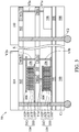
- FIGS. 1-3 illustrate schematic cross-sectional views of a semiconductor device, in accordance with some embodiments of the present disclosure.
- semiconductor device 10 includes a substrate 100 and at least one capacitor element 104 on the substrate 100.
- the substrate 100 may include an elementary (single element) semiconductor, such as silicon or germanium in a crystalline structure; a compound semiconductor, such as silicon carbide (SiC), gallium arsenide (GaAs), gallium phosphide (GaP), indium phosphide (InP), indium arsenide (InAs), and/or indium antimonide (InSb); an alloy semiconductor such as SiGe, GeC, GaAsP, AlInAs, AlGaAs, GaInAs, GaInP, and/or GaInAsP; a non-semiconductor material, such as soda-lime glass, fused silica, fused quartz, and/or calcium fluoride (CaF 2 ); and/or combinations
- the capacitor element 104 includes a first electrode 111 and a second electrode 112.
- the first electrode 111 and the second electrode 112 are formed as a first comb-shaped structure and a second comb-shaped structure, respectively.
- the first electrode 111 is configured to have a first pad 111P and a plurality of first terminals 111T connected to the first pad 111P.
- the first terminals 111T extend away from the substrate 100.
- the second electrode 112 is configured to have a second pad 112P and second terminals 112T connected to the second pad 112P.
- the second terminals 112T extend toward the substrate 100.
- the extension directions of the first terminals 111T and the second terminals 112T are parallel. As shown in FIG.
- the first terminals 111T and the second terminals 112T are staggered and separated by an interlayer dielectric layer 106.
- the terminals 111T and the second terminals 112T are alternately arranged in a horizontal direction parallel to the surface of the substrate 100 and extend between the first pad 111P and the second pad 112P in a vertical direction with respect to the surface of the substrate 100.
- the capacitor element 104 could be contained in a memory module, for example, a DRAM cell, but not limited.
- the method of forming the capacitor element 104 includes (but not limited to) depositing and patterning a material layer for the first pad 111P, depositing and patterning a material layer for the first terminals 111T on the first pad 111P (thereby forming the first electrode 111 of the capacitor element 104), depositing a material layer for the interlayer dielectric layer 106, patterning the material layer for the interlayer dielectric layer 106 to form openings, depositing a material layer for the second terminals 112T in the openings, depositing and patterning a material layer for the second pad 112P on the second terminals 112T (thereby forming the second electrode 112 of the capacitor element 104).
- patterning the material layer for the interlayer dielectric layer 106 to form openings may include etching (e.g. dry etching, wet etching, reactive ion etching (RIE)) the material layer to form the openings.
- etching e.g. dry etching, wet etching, reactive ion etching (RIE)
- RIE reactive ion etching
- a planarization process such as chemical mechanical polishing (CMP) process may be performed to remove excess material layer for the second terminals 112T outside the openings after depositing the material layer for the second terminals 112T in the openings.
- the material of the first pad 111P and the second pad 112P may include a conductive material, such as metal, metal nitride, metal oxide, metal alloy, doped polysilicon or another suitable conductive material, a combination thereof.
- the metal may include Au, Ni, Pt, Pd, Ir, Ti, Cr, W, Al, Cu, or another suitable material;
- the metal nitride may include MoN, WN, TiN, TaN, TaSiN, TaCN, TiAIN, or another suitable material.
- the first pad 111P and the second pad 112P may include the same material. In other embodiments, the first pad 111P and the second pad 112P may include different materials.
- the material layer for the first pad 111P and the second pad 112P may be deposited by chemical vapor deposition (CVD) process, physical vapor deposition (PVD) process, atomic layer deposition (ALD) process, or the like.
- the material of the first terminals 111T and the second terminals 112T may be high-k material including, for example, metal oxide or metal nitride.
- the high-k material may include HfO 2 , HfSiO, HfSiON, HfTaO, HfTiO, HfZrO, zirconium oxide, aluminum oxide, hafnium dioxide-alumina (HfO 2 -Al 2 O 3 ) alloy, other suitable high-k dielectric materials, and/or combinations thereof.
- the material layer for the first terminals 111T and the second terminals 112T may be deposited by any suitable method, such as CVD process, plasma-enhanced CVD (PECVD) process, spin-on-glass process, a combination thereof, or the like.
- the first terminals 111T and the second terminals 112T may include the same material.
- first terminals 111T and the second terminals 112T may include different materials.
- first pad 111P and the second pad 112P may each include Cu, W, or SiGe, and the first terminals 111T and the second terminals 112T may each include TiN or TaN.
- the interlayer dielectric layer 106 may include a dielectric material (e.g., a semiconductor oxide, a semiconductor nitride, a semiconductor oxynitride, a semiconductor carbide, etc.), SOG, fluoride-doped silicate glass (FSG), phosphosilicate glass (PSG), borophosphosilicate glass (BPSG), , xerogel, aerogel, amorphous fluorinated carbon, parylene, benzocyclobutene (BCB), and/or combinations thereof.
- the interlayer dielectric layer 106 may be form by CVD process, ALD process, PECVD process, high-density CVD process, PVD process, one or more other applicable processes, or a combination thereof.
- the semiconductor device 10 includes a dielectric layer 101 disposed between the substrate 100 and the capacitor element 104.
- the dielectric layer 101 may be single layer or multilayer structure including dielectric material formed of semiconductor oxide, semiconductor nitride, semiconductor oxynitride, semiconductor carbide or combinations thereof.
- the dielectric layer 101 may be formed by CVD process, ALD process, PVD process, one or more other applicable processes, or a combination thereof.
- the semiconductor device 10 includes a plurality of capacitor elements 104 successively stacked on the substrate 100.
- the capacitor elements 104 are successively stacked on the dielectric layer 101.
- the successively stacked capacitor elements 104 with the first electrode 111 and the second electrode 112 may form more compact capacitors and may be used as decoupling capacitors to provide a higher capacitance than conventional decoupling capacitors.
- the capacitance provided by the capacitor elements 104 of some embodiments of the present disclosure may be greater than 2.5 times of the capacitance provided by a conventional decoupling capacitor.
- the conventional decoupling capacitor (such as cylinder-shaped or plate-shaped decoupling capacitor) of thickness 100 ⁇ m may provide a value about 600-1300 nF/mm 2 (capacitance/area), while the capacitor elements 104 having the first electrode 111 and the second electrode 112 of thickness less than 100 ⁇ m may provide a value greater than 1200-2600 nF/mm 2 (capacitance/area).
- the capacitor elements 104 of some embodiments of the present disclosure has a higher value of capacitance/area and a smaller thickness and may be used as a decoupling capacitor for semiconductor device 10. As a result, power supply noises in the semiconductor device 10 may be prevented due to higher value of capacitance/area provided by the capacitor elements 104. Furthermore, since the thickness of the semiconductor device 10 with the decoupling capacitor (i.e. the capacitor elements 104) is reduced, the parasitic inductance and resistance will be reduced.
- the semiconductor device 10 may include one or more dielectric layers 102 between a lower one of the capacitor elements 104 and an upper one of the capacitor elements 104. As shown in FIG. 1 , conductive layers M1a/M1b, M2a/M2b, and M3a/M3b are disposed in the respective dielectric layers 102, and vias V1a/V1b, V2a/V2b, and V3a/V3b are disposed in the respective interlayer dielectric layers 106.
- the first pad 111P of the lower one of the capacitor elements 104 is connected to the second pad 112P of the upper one of the capacitor elements 104 through, for example, the via V1b, the conductive layer M1b, and the via V2b, and the second pad 112P of the lower one of the capacitor elements 104 is connected to the first pad 111P of the upper one of the capacitor elements 104 through, for example, the via V1a and the conductive layer M1a.
- the number of capacitor elements 104 successively stacked on the substrate 100 is not particularly limited. The number may be two, six, twenty one, or up to fifty or more. In some embodiments, the overall thickness of the semiconductor device 10 with the capacitor elements 104 is less than 150 ⁇ m.
- the successively stacked capacitor elements 104 may form a high-density decoupling capacitor in the semiconductor device 10 and provide a greater capacitance than conventional decoupling capacitors.
- the thickness of the decoupling capacitor formed by the capacitor elements 104 is less than the conventional decoupling capacitors. Therefore, the resulting semiconductor device with the capacitor elements 104 is thinner than those semiconductor devices with conventional decoupling capacitors and a better heat dissipation of the resulting semiconductor device may be achieved.
- the capacitor elements 104 and an IC element 108 may be integrated on the same substrate 100.
- the separation mark S represents one or more elements may be disposed between the capacitor elements 104 and the IC element 108, or, in some embodiments, the capacitor elements 104 is adjacent to the IC element 108 and no other element is disposed therebetween.
- the IC element 108 may include a memory device, a graphics processing unit (GPU), a central processing unit (CPU), or any other processing unit or control unit.
- the IC element 108 may be connected to the capacitor elements 104 via interconnections (not shown) to prevent noise from the power supply of the IC element 108. It should be noted that the IC element 108 disposed between dielectric layer 101 and dielectric layer 102 is merely illustrative. In some embodiments, the IC element 108 may be disposed on the dielectric layer 102 and be substantially on the same level as the capacitor elements 104. In some embodiments, the IC element 108 may be connected to another element through the via V1c, the conductive layer M1c, the via V2c, and the conductive layer M2c.
- the semiconductor device 10 includes a main logic die containing IC elements 110 and 114 attached on the dielectric layer 102, in accordance with some embodiments of the present disclosure.
- the IC elements 110 and 114 may include memory, a graphics processing unit (GPU), a central processing unit (CPU), or a combination thereof.
- the semiconductor device 10 may include connection features C1 and C2 which penetrate through the substrate 100. In further embodiments, the connection features C1 and C2 penetrate through the dielectric layer 102, the interlayer dielectric layer 106, the dielectric layer 101 and the substrate 100, and extend beneath a bottom surface of the substrate 100.
- connection features C1 and C2 may be connected to respective solder bumps below the substrate 100.
- the connection features C1 and C2 may be connected to the IC elements 114 and 110 respectively.
- the connection features C1 and C2 may be bonded to, for example, a printed circuit board (PCB).
- the second pad 111P of one of the capacitor elements 104 may be connected to the connection feature C1.
- the connection features C1 and C2 may be formed by a method including through silicon via (TSV) technique.
- TSV through silicon via
- the semiconductor device 10 may include plural sets of the capacitor elements 104 disposed on the substrate 100, and each of the plural sets of the capacitor elements may be respectively connected to components heterogeneously integrated in the semiconductor device 10. Accordingly, the plural sets of the capacitor elements 104 may be used as decoupling capacitors to provide higher capacitance for the components. Furthermore, the thickness of the semiconductor device 10 with the plural sets of the capacitor elements (used as decoupling capacitors) is less than the thickness of the semiconductor device with the conventional decoupling capacitors.
- one embodiment of the present disclosure may provide a decoupling capacitor of thickness equal to or less than 100 ⁇ m with a value greater than 2600 nF/mm 2 (capacitance/area), while the thickness of the conventional decoupling capacitor may need to be greater than 260 ⁇ m so that a value greater than 2600 nF/mm 2 (capacitance/area) may be achieved. Therefore, according to some embodiments of the present disclosure, parasitic inductance and resistance of heterogeneous integration with decoupling capacitors may be reduced by providing thinner decoupling capacitors.
- the IC element 108 may include memory and the IC element 110 may include CPU. In such embodiments, the performance of the semiconductor device may be improved due to shorter physical path for data communication between CPU and memory.
- FIGS. 4-6 illustrate schematic cross-sectional views of a semiconductor device, in accordance with other embodiments of the present disclosure.
- the semiconductor device 20 includes the substrate 100 and at least one capacitor element 104 on each of the opposite surfaces of the substrate 100.
- the capacitor element 104 of the semiconductor device 20 includes a first electrode 111 and a second electrode 112.
- the first electrode 111 is configured to have a first pad 111P and first terminals 111T connected to the first pad 111P.
- the first terminals 111T extend away from the substrate 100.
- the second electrode 112 is configured to have a second pad 112P and second terminals 112T connected to the second pad 112P.
- the second terminals 112T extend toward the substrate 100.
- the first terminals 111T and the second terminals 112T are staggered and separated by the interlayer dielectric layer 106.
- the material of the first pad 111P and the second pad 112P may include a conductive material, such as metal, metal nitride, metal oxide, metal alloy, another suitable conductive material, a combination thereof.
- the material of the first terminals 111T and the second terminals 112T may be high-k material including, for example, metal oxide or metal nitride.
- the method of forming the capacitor element 104 of the semiconductor device 20 is similar to the method described above with respect the semiconductor device 10 in FIG. 1 .
- the capacitor element 104 includes a plurality of capacitor elements 104 successively stacked on each of the opposite surfaces the substrate 100. In some embodiments, the sum of the thickness of each of the capacitor elements 104 is less than 100 ⁇ m. In some embodiments, the thickness of each of the capacitor elements 104 is about 2 ⁇ m. In some embodiments, the thickness of the semiconductor device 20 with the capacitor elements 104 is less than 150 ⁇ m.
- the successively stacked capacitor elements 104 may form high-density capacitors on the opposite surfaces of the substrate 100 and may be used as decoupling capacitors to provide higher capacitance than conventional decoupling capacitors. Therefore, power supply noises in the semiconductor device 20 may be prevented more effectively than conventional decoupling capacitors.
- the semiconductor device 20 may include one or more dielectric layers 102 between a lower one of the capacitor elements 104 and an upper one of the capacitor elements 104. As shown in FIG. 4 , conductive layers M1a/M1b and conductive layers M2a/M2b are disposed in the respective dielectric layers 102, and vias V1b, V2b, V3b, and V4b are disposed in the respective interlayer dielectric layers 106.
- the first pad 111P of the lower one of the capacitor elements 104 is connected to the second pad 112P of the upper one of the capacitor elements 104 through, for example, the via V1b, the conductive layer M1b, and the via V2b, and the second pad 112P of the lower one of the capacitor elements 104 is connected to the first pad 111P of the upper one of the capacitor elements 104 through, for example, the conductive layer M1a.
- the first pad 111P of the lower one of the capacitor elements 104 is connected to the second pad 112P of the upper one of the capacitor elements 104 through, for example, the via V3b, the conductive layer M2b, and the via V4b, and the second pad 112P of the lower one of the capacitor elements 104 is connected to the first pad 111P of the upper one of the capacitor elements 104 through, for example, the conductive layer M2a.
- the number of capacitor elements 104 successively stacked on the opposite surfaces of the substrate 100 is not particularly limited. The number may be one, eleven, thirty, or up to fifty or more.
- the embodiment describes a hybrid structure formed by techniques of at least two wafers bonding
- the semiconductor device 20 includes a main logic die containing an IC element 116 attached on the dielectric layer 102, in accordance with other embodiments of the present disclosure.
- the IC element 116 may include memory, a graphics processing unit (GPU), a central processing unit (CPU), or a combination thereof.
- the semiconductor device 20 may include connection features C3, C4, and C5 which may be bonded to, for example, a printed circuit board (PCB).
- PCB printed circuit board
- connection features connection features C3, C4, and C5 may be formed by a method including through silicon via (TSV) technique.
- TSV through silicon via
- the second pad 112P of the lower one of the capacitor elements 104 is connected to the first pad 111P of the upper one of the capacitor elements 104 through the connection feature C4 in some embodiments.
- the embodiment describes a hybrid structure formed by techniques of at least three wafers bonding
- the semiconductor device 20 includes a main logic die containing an IC element 117 attached to the interlayer dielectric layer 106 on the upper surface of the substrate 100 and another main logic die containing an IC element 118 attached to the interlayer dielectric layer 106 under the lower surface of the substrate 100, in accordance with other embodiments of the present disclosure.
- the main logic die containing an IC element 117 is attached to the interlayer dielectric layer 106 on the topmost capacitor element 104 and the main logic die containing an IC element 118 is attached to the interlayer dielectric layer 106 under the bottommost capacitor element 104.
- the semiconductor device 20 may include an IC element 120 connected to the IC element 117 through via V3c and an IC element 122 connected to the IC element 118 through via V1c.
- FIG. 6 illustrates another example of heterogeneous integration, where two main logic dies are respectively attached to the respective interlayer dielectric layers 106 above and/or below the least one capacitor element on the opposite surfaces of the substrate 100, in accordance with some embodiments of the present disclosure.
- the semiconductor device 20 may be thinner and more compact since the components are integrated on opposite sides of the same substrate 100, and the communication between components is more efficient due to shorter physical paths among the components are provided.
- the embodiments of the present disclosure provide many benefits to a semiconductor device.
- the power supply noises in the semiconductor device may be prevented by the capacitor elements more effectively and a stable power supply is achieved.
- the capacitor elements may form high-density decoupling capacitors to provide thinner decoupling capacitors for the semiconductor device. In addition, this may improve heat dissipation in the semiconductor device with decoupling capacitors.
Landscapes
- Semiconductor Integrated Circuits (AREA)
- Engineering & Computer Science (AREA)
- Power Engineering (AREA)
- Bipolar Transistors (AREA)
- Noodles (AREA)
- Die Bonding (AREA)
Abstract
Description
- This application claims the benefit of
U.S. Provisional Application No. 63/034,450 filed on June 4, 2020 - The present disclosure relates to a semiconductor device, and in particular, to a semiconductor device with a capacitor element.
- Semiconductor devices can be applied in various fields, such as smart TVs, voice assistant devices (VAD), tablets, feature phones, smartphones, optical and Blu-ray DVD players, and so on. Semiconductor devices are typically manufactured in the following manner: sequentially depositing an insulation or dielectric layer, a conductive layer, and a semiconductor material layer on a semiconductor substrate, and patterning the various material layers by using lithography and etching technique to forming circuit components and elements thereon.
- In an effort to continue the scaling-down process of semiconductor devices, the functional density (i.e., the number of interconnected devices per chip area) has generally increased while geometric size (i.e., the smallest component (or line) that can be created using the fabrication process) has decreased. This scaling-down process generally provides benefits by improving production efficiency and performance of semiconductor devices, and lowering associated costs as well. Such scaling down has also been accompanied by increased complexity in design and manufacturing of semiconductor devices. Parallel advances in manufacturing have allowed increasingly complex designs to be fabricated with precision and reliability.
- However, numerous challenges have arisen in the effort to continue the scaling-down of semiconductor devices. For example, fluctuations (or noises) in power supply (or being referred to power supply noise) adversely affect performance of semiconductor devices. To reduce power supply noise, decoupling capacitors may be integrated into semiconductor devices and used as charge reservoirs to prevent unwanted drop or rise in power supply. Existing decoupling capacitors for semiconductor devices have been generally adequate for their intended purposes, but they have not been entirely satisfactory in all respects.
- Some embodiments of the present disclosure provide a semiconductor device. An embodiment of the present disclosure provides a semiconductor device, which includes a substrate and at least one capacitor element. The capacitor element is on the substrate. The capacitor element includes a first electrode with a first pad and first terminals connected to the first pad, wherein the first terminals extend away from the substrate; and a second electrode with a second pad and second terminals connected to the second pad, wherein the second terminals extend toward the substrate, wherein the first terminals and the second terminals are staggered and separated by an interlayer dielectric layer.
- Another embodiment of the present disclosure provides a semiconductor device, which includes a substrate and at least one capacitor element on each of the opposite surfaces of the substrate. Each capacitor element includes a first electrode with a first pad and first terminals connected to the first pad, wherein the first terminals extend away from the substrate; and a second electrode with a second pad and second terminals connected to the second pad, wherein the second terminals extend toward the substrate, wherein the first terminals and the second terminals are staggered and separated by an interlayer dielectric layer.
- Aspects of the present disclosure are best understood from the following detailed description when read with the accompanying figures. It is emphasized that, in accordance with the standard practice in the industry, various features are not drawn to scale. In fact, the dimensions of the various features may be arbitrarily increased or reduced for clarity of discussion.
-
FIGS. 1-3 illustrate schematic cross-sectional views of a semiconductor device, in accordance with some embodiments of the present disclosure. -
FIGS. 4-6 illustrate schematic cross-sectional views of a semiconductor device, in accordance with other embodiments of the present disclosure. - The following disclosure provides many different embodiments, or examples, for implementing different features of the provided subject matter. Specific examples of components and arrangements are described below to simplify the present disclosure. These are, of course, merely examples and are not intended to be limiting. For example, the formation of a first feature over or on a second feature in the description that follows may include embodiments in which the first and second features are formed in direct contact, and may also include embodiments in which additional features may be formed between the first and second features, such that the first and second features may not be in direct contact. In addition, the present disclosure may repeat reference numerals and/or letters in the various examples. This repetition is for the purpose of simplicity and clarity and does not in itself dictate a relationship between the various embodiments and/or configurations discussed.
- Additionally, in some embodiments of the present disclosure, terms concerning attachments, coupling and the like, such as "connected" and "interconnected", refer to a relationship wherein structures are secured or attached to one another either directly or indirectly through intervening structures, as well as both movable or rigid attachments or relationships, unless expressly described otherwise. In addition, the term "coupled" include any method of direct and indirect electrical connection.
- Further, spatially relative terms, such as "beneath," "below," "lower," "above," "upper" and the like, may be used herein for ease of description to describe one element or feature's relationship to another element or feature as illustrated in the figures. The spatially relative terms are intended to encompass different orientations of the device in use or operation in addition to the orientation depicted in the figures. The apparatus may be otherwise oriented (rotated 90 degrees or at other orientations) and the spatially relative descriptors used herein may likewise be interpreted accordingly.
- The terms "about", "approximately", and "roughly" typically mean ±20% of the stated value, or ±10% of the stated value, or ±5% of the stated value, or ±3% of the stated value, or ±2% of the stated value, or ±1% of the stated value, or ±0.5% of the stated value. The stated value of the present disclosure is an approximate value. When there is no specific description, the stated value includes the meaning of "about", "approximately", and "roughly". The terminology used herein is for the purpose of describing particular embodiments only and is not intended to limit the invention. As used herein, the singular terms "a," "an" and "the" are intended to include the plural forms as well, unless the context clearly indicates otherwise.
- Some embodiments of the disclosure are described below. Additional operations can be provided before, during, and/or after the stages described in these embodiments. Some of the stages that are described can be replaced or eliminated for different embodiments. Additional features can be added to the semiconductor device structure. Some of the features described below can be replaced or eliminated for different embodiments. Although some embodiments are discussed with operations performed in a particular order, these operations may be performed in another logical order.
- As the performance of semiconductor devices have been improved, larger currents at higher frequencies but with lower power supply are demanded by these high-performance semiconductor devices. In such conditions, the design of power system becomes increasingly challenging. For example, the impact of power supply noise on the performance of semiconductor devices is critical and should be addressed. The present disclosure provides a semiconductor device with at least one capacitor element as a decoupling capacitor to prevent power supply noise (such as unwanted rise or drop in power supply) in the semiconductor device. In some embodiments, a high-density capacitor element is provided to achieve higher capacitance for the decoupling capacitor and higher compactness of the semiconductor device.
-
FIGS. 1-3 illustrate schematic cross-sectional views of a semiconductor device, in accordance with some embodiments of the present disclosure. Referring toFIG. 1 ,semiconductor device 10 includes asubstrate 100 and at least onecapacitor element 104 on thesubstrate 100. Thesubstrate 100 may include an elementary (single element) semiconductor, such as silicon or germanium in a crystalline structure; a compound semiconductor, such as silicon carbide (SiC), gallium arsenide (GaAs), gallium phosphide (GaP), indium phosphide (InP), indium arsenide (InAs), and/or indium antimonide (InSb); an alloy semiconductor such as SiGe, GeC, GaAsP, AlInAs, AlGaAs, GaInAs, GaInP, and/or GaInAsP; a non-semiconductor material, such as soda-lime glass, fused silica, fused quartz, and/or calcium fluoride (CaF2); and/or combinations thereof. For example, the material of the elementary semiconductor may include monocrystalline silicon (Si), polycrystalline silicon (poly-Si), amorphous silicon (a-Si), germanium (Ge), and/or carbon (C) (e.g. diamond). - The
capacitor element 104 includes afirst electrode 111 and asecond electrode 112. In some embodiments, thefirst electrode 111 and thesecond electrode 112 are formed as a first comb-shaped structure and a second comb-shaped structure, respectively. Thefirst electrode 111 is configured to have afirst pad 111P and a plurality offirst terminals 111T connected to thefirst pad 111P. Thefirst terminals 111T extend away from thesubstrate 100. Thesecond electrode 112 is configured to have asecond pad 112P andsecond terminals 112T connected to thesecond pad 112P. Thesecond terminals 112T extend toward thesubstrate 100. In some embodiments, the extension directions of thefirst terminals 111T and thesecond terminals 112T are parallel. As shown inFIG. 1 , thefirst terminals 111T and thesecond terminals 112T are staggered and separated by aninterlayer dielectric layer 106. In some embodiments, theterminals 111T and thesecond terminals 112T are alternately arranged in a horizontal direction parallel to the surface of thesubstrate 100 and extend between thefirst pad 111P and thesecond pad 112P in a vertical direction with respect to the surface of thesubstrate 100. In some embodiments, thecapacitor element 104 could be contained in a memory module, for example, a DRAM cell, but not limited. - In some embodiments, the method of forming the
capacitor element 104 includes (but not limited to) depositing and patterning a material layer for thefirst pad 111P, depositing and patterning a material layer for thefirst terminals 111T on thefirst pad 111P (thereby forming thefirst electrode 111 of the capacitor element 104), depositing a material layer for theinterlayer dielectric layer 106, patterning the material layer for theinterlayer dielectric layer 106 to form openings, depositing a material layer for thesecond terminals 112T in the openings, depositing and patterning a material layer for thesecond pad 112P on thesecond terminals 112T (thereby forming thesecond electrode 112 of the capacitor element 104). In some embodiments, patterning the material layer for theinterlayer dielectric layer 106 to form openings may include etching (e.g. dry etching, wet etching, reactive ion etching (RIE)) the material layer to form the openings. In some embodiments, a planarization process such as chemical mechanical polishing (CMP) process may be performed to remove excess material layer for thesecond terminals 112T outside the openings after depositing the material layer for thesecond terminals 112T in the openings. - The material of the
first pad 111P and thesecond pad 112P may include a conductive material, such as metal, metal nitride, metal oxide, metal alloy, doped polysilicon or another suitable conductive material, a combination thereof. For example, the metal may include Au, Ni, Pt, Pd, Ir, Ti, Cr, W, Al, Cu, or another suitable material; the metal nitride may include MoN, WN, TiN, TaN, TaSiN, TaCN, TiAIN, or another suitable material. In some embodiments, thefirst pad 111P and thesecond pad 112P may include the same material. In other embodiments, thefirst pad 111P and thesecond pad 112P may include different materials. The material layer for thefirst pad 111P and thesecond pad 112P may be deposited by chemical vapor deposition (CVD) process, physical vapor deposition (PVD) process, atomic layer deposition (ALD) process, or the like. The material of thefirst terminals 111T and thesecond terminals 112T may be high-k material including, for example, metal oxide or metal nitride. In some embodiments, the high-k material may include HfO2, HfSiO, HfSiON, HfTaO, HfTiO, HfZrO, zirconium oxide, aluminum oxide, hafnium dioxide-alumina (HfO2-Al2O3) alloy, other suitable high-k dielectric materials, and/or combinations thereof. The material layer for thefirst terminals 111T and thesecond terminals 112T may be deposited by any suitable method, such as CVD process, plasma-enhanced CVD (PECVD) process, spin-on-glass process, a combination thereof, or the like. In some embodiments, thefirst terminals 111T and thesecond terminals 112T may include the same material. In other embodiments, thefirst terminals 111T and thesecond terminals 112T may include different materials. According to some embodiments of the present disclosure, thefirst pad 111P and thesecond pad 112P may each include Cu, W, or SiGe, and thefirst terminals 111T and thesecond terminals 112T may each include TiN or TaN. - The interlayer dielectric layer 106 (or may be referred to inter-metal dielectric (IMD) may include a dielectric material (e.g., a semiconductor oxide, a semiconductor nitride, a semiconductor oxynitride, a semiconductor carbide, etc.), SOG, fluoride-doped silicate glass (FSG), phosphosilicate glass (PSG), borophosphosilicate glass (BPSG), , xerogel, aerogel, amorphous fluorinated carbon, parylene, benzocyclobutene (BCB), and/or combinations thereof. The
interlayer dielectric layer 106 may be form by CVD process, ALD process, PECVD process, high-density CVD process, PVD process, one or more other applicable processes, or a combination thereof. - In some embodiments, the
semiconductor device 10 includes adielectric layer 101 disposed between thesubstrate 100 and thecapacitor element 104. Thedielectric layer 101 may be single layer or multilayer structure including dielectric material formed of semiconductor oxide, semiconductor nitride, semiconductor oxynitride, semiconductor carbide or combinations thereof. Thedielectric layer 101 may be formed by CVD process, ALD process, PVD process, one or more other applicable processes, or a combination thereof. - According to some embodiments of the present disclosure, the
semiconductor device 10 includes a plurality ofcapacitor elements 104 successively stacked on thesubstrate 100. In some embodiments, thecapacitor elements 104 are successively stacked on thedielectric layer 101. The successively stackedcapacitor elements 104 with thefirst electrode 111 and thesecond electrode 112 may form more compact capacitors and may be used as decoupling capacitors to provide a higher capacitance than conventional decoupling capacitors. The capacitance provided by thecapacitor elements 104 of some embodiments of the present disclosure may be greater than 2.5 times of the capacitance provided by a conventional decoupling capacitor. For example, the conventional decoupling capacitor (such as cylinder-shaped or plate-shaped decoupling capacitor) ofthickness 100 µm may provide a value about 600-1300 nF/mm2 (capacitance/area), while thecapacitor elements 104 having thefirst electrode 111 and thesecond electrode 112 of thickness less than 100 µm may provide a value greater than 1200-2600 nF/mm2 (capacitance/area). Thecapacitor elements 104 of some embodiments of the present disclosure has a higher value of capacitance/area and a smaller thickness and may be used as a decoupling capacitor forsemiconductor device 10. As a result, power supply noises in thesemiconductor device 10 may be prevented due to higher value of capacitance/area provided by thecapacitor elements 104. Furthermore, since the thickness of thesemiconductor device 10 with the decoupling capacitor (i.e. the capacitor elements 104) is reduced, the parasitic inductance and resistance will be reduced. - In some embodiments, the
semiconductor device 10 may include one or moredielectric layers 102 between a lower one of thecapacitor elements 104 and an upper one of thecapacitor elements 104. As shown inFIG. 1 , conductive layers M1a/M1b, M2a/M2b, and M3a/M3b are disposed in the respectivedielectric layers 102, and vias V1a/V1b, V2a/V2b, and V3a/V3b are disposed in the respective interlayer dielectric layers 106. In some embodiments, thefirst pad 111P of the lower one of thecapacitor elements 104 is connected to thesecond pad 112P of the upper one of thecapacitor elements 104 through, for example, the via V1b, the conductive layer M1b, and the via V2b, and thesecond pad 112P of the lower one of thecapacitor elements 104 is connected to thefirst pad 111P of the upper one of thecapacitor elements 104 through, for example, the via V1a and the conductive layer M1a. The number ofcapacitor elements 104 successively stacked on thesubstrate 100 is not particularly limited. The number may be two, six, twenty one, or up to fifty or more. In some embodiments, the overall thickness of thesemiconductor device 10 with thecapacitor elements 104 is less than 150 µm. The successively stackedcapacitor elements 104 may form a high-density decoupling capacitor in thesemiconductor device 10 and provide a greater capacitance than conventional decoupling capacitors. In addition, the thickness of the decoupling capacitor formed by thecapacitor elements 104 is less than the conventional decoupling capacitors. Therefore, the resulting semiconductor device with thecapacitor elements 104 is thinner than those semiconductor devices with conventional decoupling capacitors and a better heat dissipation of the resulting semiconductor device may be achieved. - Referring to
FIG. 2 , thecapacitor elements 104 and anIC element 108 may be integrated on thesame substrate 100. For simplicity, like features inFIG. 2 andFIG. 1 are designated with like reference numerals and some of the description is not repeated. The separation mark S represents one or more elements may be disposed between thecapacitor elements 104 and theIC element 108, or, in some embodiments, thecapacitor elements 104 is adjacent to theIC element 108 and no other element is disposed therebetween. TheIC element 108 may include a memory device, a graphics processing unit (GPU), a central processing unit (CPU), or any other processing unit or control unit. In some embodiments, theIC element 108 may be connected to thecapacitor elements 104 via interconnections (not shown) to prevent noise from the power supply of theIC element 108. It should be noted that theIC element 108 disposed betweendielectric layer 101 anddielectric layer 102 is merely illustrative. In some embodiments, theIC element 108 may be disposed on thedielectric layer 102 and be substantially on the same level as thecapacitor elements 104. In some embodiments, theIC element 108 may be connected to another element through the via V1c, the conductive layer M1c, the via V2c, and the conductive layer M2c. - Referring to
FIG. 3 , thesemiconductor device 10 includes a main logic die containingIC elements dielectric layer 102, in accordance with some embodiments of the present disclosure. For simplicity, like features inFIG. 3 andFIGS. 1 and2 are designated with like reference numerals and some of the description is not repeated. TheIC elements semiconductor device 10 may include connection features C1 and C2 which penetrate through thesubstrate 100. In further embodiments, the connection features C1 and C2 penetrate through thedielectric layer 102, theinterlayer dielectric layer 106, thedielectric layer 101 and thesubstrate 100, and extend beneath a bottom surface of thesubstrate 100. In some embodiments, the connection features C1 and C2 may be connected to respective solder bumps below thesubstrate 100. In some embodiments, the connection features C1 and C2 may be connected to theIC elements second pad 111P of one of thecapacitor elements 104 may be connected to the connection feature C1. In some embodiment, the connection features C1 and C2 may be formed by a method including through silicon via (TSV) technique. The main logic die includingIC elements capacitor elements 104, theIC element 108 are integrated on thesame substrate 100. This integration may be referred to heterogeneous integration, which represents an integration of system on chips (SoC), memories, power supply, power management, and/or other components. In some embodiments, thesemiconductor device 10 may include plural sets of thecapacitor elements 104 disposed on thesubstrate 100, and each of the plural sets of the capacitor elements may be respectively connected to components heterogeneously integrated in thesemiconductor device 10. Accordingly, the plural sets of thecapacitor elements 104 may be used as decoupling capacitors to provide higher capacitance for the components. Furthermore, the thickness of thesemiconductor device 10 with the plural sets of the capacitor elements (used as decoupling capacitors) is less than the thickness of the semiconductor device with the conventional decoupling capacitors. For example, one embodiment of the present disclosure may provide a decoupling capacitor of thickness equal to or less than 100 µm with a value greater than 2600 nF/mm2 (capacitance/area), while the thickness of the conventional decoupling capacitor may need to be greater than 260 µm so that a value greater than 2600 nF/mm2 (capacitance/area) may be achieved. Therefore, according to some embodiments of the present disclosure, parasitic inductance and resistance of heterogeneous integration with decoupling capacitors may be reduced by providing thinner decoupling capacitors. In some embodiments, theIC element 108 may include memory and theIC element 110 may include CPU. In such embodiments, the performance of the semiconductor device may be improved due to shorter physical path for data communication between CPU and memory. -
FIGS. 4-6 illustrate schematic cross-sectional views of a semiconductor device, in accordance with other embodiments of the present disclosure. Referring toFIG. 4 , thesemiconductor device 20 includes thesubstrate 100 and at least onecapacitor element 104 on each of the opposite surfaces of thesubstrate 100. For simplicity, like features insemiconductor device 20 andsemiconductor device 10 are designated with like reference numerals and some of the description is not repeated. Thecapacitor element 104 of thesemiconductor device 20 includes afirst electrode 111 and asecond electrode 112. Thefirst electrode 111 is configured to have afirst pad 111P andfirst terminals 111T connected to thefirst pad 111P. Thefirst terminals 111T extend away from thesubstrate 100. Thesecond electrode 112 is configured to have asecond pad 112P andsecond terminals 112T connected to thesecond pad 112P. Thesecond terminals 112T extend toward thesubstrate 100. As shown inFIG. 4 , thefirst terminals 111T and thesecond terminals 112T are staggered and separated by theinterlayer dielectric layer 106. The material of thefirst pad 111P and thesecond pad 112P may include a conductive material, such as metal, metal nitride, metal oxide, metal alloy, another suitable conductive material, a combination thereof. The material of thefirst terminals 111T and thesecond terminals 112T may be high-k material including, for example, metal oxide or metal nitride. The method of forming thecapacitor element 104 of thesemiconductor device 20 is similar to the method described above with respect thesemiconductor device 10 inFIG. 1 . - In some embodiments, the
capacitor element 104 includes a plurality ofcapacitor elements 104 successively stacked on each of the opposite surfaces thesubstrate 100. In some embodiments, the sum of the thickness of each of thecapacitor elements 104 is less than 100 µm. In some embodiments, the thickness of each of thecapacitor elements 104 is about 2 µm. In some embodiments, the thickness of thesemiconductor device 20 with thecapacitor elements 104 is less than 150 µm. The successively stackedcapacitor elements 104 may form high-density capacitors on the opposite surfaces of thesubstrate 100 and may be used as decoupling capacitors to provide higher capacitance than conventional decoupling capacitors. Therefore, power supply noises in thesemiconductor device 20 may be prevented more effectively than conventional decoupling capacitors. - In some embodiments, the
semiconductor device 20 may include one or moredielectric layers 102 between a lower one of thecapacitor elements 104 and an upper one of thecapacitor elements 104. As shown inFIG. 4 , conductive layers M1a/M1b and conductive layers M2a/M2b are disposed in the respectivedielectric layers 102, and vias V1b, V2b, V3b, and V4b are disposed in the respective interlayer dielectric layers 106. In some embodiments, forcapacitor elements 104 below the lower surface of thesemiconductor device 20, thefirst pad 111P of the lower one of thecapacitor elements 104 is connected to thesecond pad 112P of the upper one of thecapacitor elements 104 through, for example, the via V1b, the conductive layer M1b, and the via V2b, and thesecond pad 112P of the lower one of thecapacitor elements 104 is connected to thefirst pad 111P of the upper one of thecapacitor elements 104 through, for example, the conductive layer M1a. Similarly, in some embodiments, forcapacitor elements 104 on the upper surface of thesemiconductor device 20, thefirst pad 111P of the lower one of thecapacitor elements 104 is connected to thesecond pad 112P of the upper one of thecapacitor elements 104 through, for example, the via V3b, the conductive layer M2b, and the via V4b, and thesecond pad 112P of the lower one of thecapacitor elements 104 is connected to thefirst pad 111P of the upper one of thecapacitor elements 104 through, for example, the conductive layer M2a. The number ofcapacitor elements 104 successively stacked on the opposite surfaces of thesubstrate 100 is not particularly limited. The number may be one, eleven, thirty, or up to fifty or more. - Referring to
FIG. 5 , the embodiment describes a hybrid structure formed by techniques of at least two wafers bonding, thesemiconductor device 20 includes a main logic die containing anIC element 116 attached on thedielectric layer 102, in accordance with other embodiments of the present disclosure. For simplicity, like features inFIG. 5 andFIG. 4 are designated with like reference numerals and some of the description is not repeated. TheIC element 116 may include memory, a graphics processing unit (GPU), a central processing unit (CPU), or a combination thereof. Thesemiconductor device 20 may include connection features C3, C4, and C5 which may be bonded to, for example, a printed circuit board (PCB). In some embodiment, the connection features connection features C3, C4, and C5 may be formed by a method including through silicon via (TSV) technique. As shown inFIG. 5 , thesecond pad 112P of the lower one of thecapacitor elements 104 is connected to thefirst pad 111P of the upper one of thecapacitor elements 104 through the connection feature C4 in some embodiments. - Referring to
FIG. 6 , the embodiment describes a hybrid structure formed by techniques of at least three wafers bonding, thesemiconductor device 20 includes a main logic die containing anIC element 117 attached to theinterlayer dielectric layer 106 on the upper surface of thesubstrate 100 and another main logic die containing anIC element 118 attached to theinterlayer dielectric layer 106 under the lower surface of thesubstrate 100, in accordance with other embodiments of the present disclosure. In some embodiments, the main logic die containing anIC element 117 is attached to theinterlayer dielectric layer 106 on thetopmost capacitor element 104 and the main logic die containing anIC element 118 is attached to theinterlayer dielectric layer 106 under thebottommost capacitor element 104. For simplicity, like features inFIG. 6 andFIG. 4 are designated with like reference numerals and some of the description is not repeated. In some embodiments, thesemiconductor device 20 may include anIC element 120 connected to theIC element 117 through via V3c and anIC element 122 connected to theIC element 118 through via V1c.FIG. 6 illustrates another example of heterogeneous integration, where two main logic dies are respectively attached to the respective interlayerdielectric layers 106 above and/or below the least one capacitor element on the opposite surfaces of thesubstrate 100, in accordance with some embodiments of the present disclosure. In such embodiments of heterogeneous integration, thesemiconductor device 20 may be thinner and more compact since the components are integrated on opposite sides of thesame substrate 100, and the communication between components is more efficient due to shorter physical paths among the components are provided. - The embodiments of the present disclosure provide many benefits to a semiconductor device. For example, the power supply noises in the semiconductor device may be prevented by the capacitor elements more effectively and a stable power supply is achieved. The capacitor elements may form high-density decoupling capacitors to provide thinner decoupling capacitors for the semiconductor device. In addition, this may improve heat dissipation in the semiconductor device with decoupling capacitors.
- The foregoing outlines features of several embodiments so that those skilled in the art may better understand the aspects of the present disclosure. Those skilled in the art should appreciate that they may readily use the present disclosure as a basis for designing or modifying other processes and structures for carrying out the same purposes and/or achieving the same advantages of the embodiments introduced herein. Those skilled in the art should also realize that such equivalent constructions do not depart from the spirit and scope of the present disclosure, and that they may make various changes, substitutions, and alterations herein without departing from the spirit and scope of the present disclosure.
Claims (15)
- A semiconductor device, comprising:a substrate; andat least one capacitor element on the substrate, wherein the at least one capacitor element comprises:a first electrode with a first pad and first terminals connected to the first pad, wherein the first terminals extend away from the substrate; anda second electrode with a second pad and second terminals connected to the second pad, wherein the second terminals extend toward the substrate, wherein the first terminals and the second terminals are staggered and separated by an interlayer dielectric layer.
- The semiconductor device as claimed in claim 1, further comprising a dielectric layer between the substrate and the at least one capacitor element.
- The semiconductor device as claimed in claim 1 or 2, wherein the at least one capacitor element comprises a plurality of capacitor elements successively stacked on the substrate.
- The semiconductor device as claimed in claim 3, wherein the first pad of a lower one of the capacitor elements is connected to the second pad of an upper one of the capacitor elements; and/or
wherein the second pad of the lower one of the capacitor elements is connected to the first pad of the upper one of the capacitor elements. - The semiconductor device as claimed in claim 3 or 4, further comprising a dielectric layer between the lower one of the capacitor elements and the upper one of the capacitor elements, and a conductive layer in the dielectric layer.
- The semiconductor device as claimed in one of the preceding claims, further comprising a first IC element on the substrate, wherein the first IC element is substantially on a same level as the at least one capacitor element;
wherein the first IC element preferably comprises memory, a graphics processing unit (GPU), a central processing unit (CPU), or a combination thereof. - The semiconductor device as claimed in claim 6, further comprising a second IC element over and connected to the first IC element, and a third IC element over the at least one capacitor element;
wherein the second IC element and the third IC element preferably each comprises memory, a graphics processing unit (GPU), a central processing unit (CPU), or a combination thereof. - The semiconductor device of one of the preceding claims comprising:
at least one capacitor element on each of opposite surfaces of the substrate. - The semiconductor device as claimed in claim 8, wherein the at least one capacitor element comprises a plurality of capacitor elements successively stacked on each of the opposite surfaces the substrate.
- The semiconductor device as claimed in claim 8 or 9, wherein a sum of a thickness of each of the capacitor elements is less than 100 µm.
- The semiconductor device as claimed in one of claims 8 to 10, further comprising a first IC element disposed above the at least one capacitor element on an upper surface of the substrate, and/or
further comprising a second IC element disposed below the at least one capacitor element under a lower surface of the substrate; and/or
further comprising a third IC element disposed above the upper surface of the substrate and/or a fourth IC element disposed below the lower surface of the substrate, wherein the third IC element is connected to the first IC element and the fourth IC element is connected to the second IC element. - The semiconductor device of one of the preceding claims comprising:a first IC element on the substrate; anda connection feature penetrating through the substrate.
- The semiconductor device as claimed in claim 12, further comprising a dielectric layer on the at least one capacitor element;
wherein the connection feature preferably penetrates through the dielectric layer and the substrate, and extends beneath a bottom surface of the substrate. - The semiconductor device as claimed in claim 12 or 13, further comprising a second IC element on the dielectric layer, wherein the connection feature is connected to the second IC element.
- The semiconductor device as claimed in one of claims 12 to 14, wherein the connection feature is connected to the first pad.
Applications Claiming Priority (2)
| Application Number | Priority Date | Filing Date | Title |
|---|---|---|---|
| US202063034450P | 2020-06-04 | 2020-06-04 | |
| US17/226,330 US11538748B2 (en) | 2020-06-04 | 2021-04-09 | Semiconductor device with capacitor element |
Publications (2)
| Publication Number | Publication Date |
|---|---|
| EP3920248A1 true EP3920248A1 (en) | 2021-12-08 |
| EP3920248B1 EP3920248B1 (en) | 2025-07-02 |
Family
ID=75728553
Family Applications (1)
| Application Number | Title | Priority Date | Filing Date |
|---|---|---|---|
| EP21170579.3A Active EP3920248B1 (en) | 2020-06-04 | 2021-04-27 | Semiconductor device with capacitor element |
Country Status (4)
| Country | Link |
|---|---|
| US (2) | US11538748B2 (en) |
| EP (1) | EP3920248B1 (en) |
| CN (1) | CN113764377A (en) |
| TW (1) | TWI806059B (en) |
Families Citing this family (5)
| Publication number | Priority date | Publication date | Assignee | Title |
|---|---|---|---|---|
| JP7654431B2 (en) | 2021-03-17 | 2025-04-01 | キオクシア株式会社 | Semiconductor device and its manufacturing method |
| KR20230123346A (en) * | 2022-02-16 | 2023-08-23 | 삼성전자주식회사 | Integrated Circuit |
| CN117393553B (en) * | 2022-07-05 | 2026-01-06 | 荣耀终端股份有限公司 | Semiconductor devices including decoupling capacitors and their manufacturing methods |
| US20240113158A1 (en) * | 2022-09-30 | 2024-04-04 | Intel Corporation | High surface area capacitor in an electronic substrate package |
| US12588291B2 (en) * | 2023-06-13 | 2026-03-24 | Intel Corporation | Substrates including micro-structured thin film capacitors |
Citations (5)
| Publication number | Priority date | Publication date | Assignee | Title |
|---|---|---|---|---|
| US20080042181A1 (en) * | 2006-08-21 | 2008-02-21 | Nec Electronics Corporation | Semiconductor device |
| KR20100085391A (en) * | 2009-01-20 | 2010-07-29 | 삼성전자주식회사 | Semiconductor device having capacitor and fabrication method thereof |
| US7960773B2 (en) * | 2008-08-29 | 2011-06-14 | Industrial Technology Research Institute | Capacitor device and method for manufacturing the same |
| US20160020267A1 (en) * | 2012-11-26 | 2016-01-21 | Taiwan Semiconductor Manufacturing Co., Ltd. | Low impedance high density deep trench capacitor |
| US20190057949A1 (en) * | 2017-08-16 | 2019-02-21 | Samsung Electronics Co., Ltd. | Semiconductor packages |
Family Cites Families (11)
| Publication number | Priority date | Publication date | Assignee | Title |
|---|---|---|---|---|
| US6391707B1 (en) * | 2001-05-04 | 2002-05-21 | Texas Instruments Incorporated | Method of manufacturing a zero mask high density metal/insulator/metal capacitor |
| KR100867038B1 (en) * | 2005-03-02 | 2008-11-04 | 삼성전기주식회사 | Capacitor embedded printed circuit board and its manufacturing method |
| FR2965942B1 (en) * | 2010-10-08 | 2013-02-22 | Commissariat Energie Atomique | LIQUID CRYSTAL DISPLAY OF TRANSMISSIVE TYPE IN CMOS TECHNOLOGY WITH AUXILIARY STORAGE CAPACITY |
| JP5754398B2 (en) * | 2012-03-09 | 2015-07-29 | 三菱電機株式会社 | Semiconductor device |
| US9331013B2 (en) * | 2013-03-14 | 2016-05-03 | Taiwan Semiconductor Manufacturing Company, Ltd. | Integrated capacitor |
| US9349788B2 (en) * | 2013-08-08 | 2016-05-24 | Zhuhai Advanced Chip Carriers & Electronic Substrate Solutions Technologies Co. Ltd. | Thin film capacitors embedded in polymer dielectric |
| US9704836B2 (en) * | 2015-03-16 | 2017-07-11 | Mediatek Inc. | Semiconductor package assembly |
| WO2019005021A1 (en) * | 2017-06-27 | 2019-01-03 | Intel Corporation | Microelectronic devices designed with ultra-high-k dielectric capacitors integrated with package substrates |
| CN109244059A (en) * | 2017-07-10 | 2019-01-18 | 中芯国际集成电路制造(上海)有限公司 | A kind of semiconductor devices and preparation method thereof, electronic device |
| KR20190017558A (en) * | 2017-08-11 | 2019-02-20 | 삼성전자주식회사 | Capacitor structure and semiconductor device having the same |
| US10446325B2 (en) * | 2017-09-29 | 2019-10-15 | Advanced Semiconductor Engineering, Inc. | Capacitor structures |
-
2021
- 2021-04-09 US US17/226,330 patent/US11538748B2/en active Active
- 2021-04-27 EP EP21170579.3A patent/EP3920248B1/en active Active
- 2021-05-31 CN CN202110603765.4A patent/CN113764377A/en active Pending
- 2021-06-01 TW TW110119760A patent/TWI806059B/en active
-
2022
- 2022-11-22 US US18/057,880 patent/US11798878B2/en active Active
Patent Citations (5)
| Publication number | Priority date | Publication date | Assignee | Title |
|---|---|---|---|---|
| US20080042181A1 (en) * | 2006-08-21 | 2008-02-21 | Nec Electronics Corporation | Semiconductor device |
| US7960773B2 (en) * | 2008-08-29 | 2011-06-14 | Industrial Technology Research Institute | Capacitor device and method for manufacturing the same |
| KR20100085391A (en) * | 2009-01-20 | 2010-07-29 | 삼성전자주식회사 | Semiconductor device having capacitor and fabrication method thereof |
| US20160020267A1 (en) * | 2012-11-26 | 2016-01-21 | Taiwan Semiconductor Manufacturing Co., Ltd. | Low impedance high density deep trench capacitor |
| US20190057949A1 (en) * | 2017-08-16 | 2019-02-21 | Samsung Electronics Co., Ltd. | Semiconductor packages |
Also Published As
| Publication number | Publication date |
|---|---|
| CN113764377A (en) | 2021-12-07 |
| TWI806059B (en) | 2023-06-21 |
| US11538748B2 (en) | 2022-12-27 |
| TW202147565A (en) | 2021-12-16 |
| US11798878B2 (en) | 2023-10-24 |
| US20230083357A1 (en) | 2023-03-16 |
| EP3920248B1 (en) | 2025-07-02 |
| US20210384117A1 (en) | 2021-12-09 |
Similar Documents
| Publication | Publication Date | Title |
|---|---|---|
| EP3920248B1 (en) | Semiconductor device with capacitor element | |
| US8890224B2 (en) | Semiconductor structures having a metal-insulator-metal capacitor structure | |
| US12356639B2 (en) | Double-sided stacked DTC structure | |
| CN220774364U (en) | Packaging structure and high bandwidth memory HBM device | |
| US12525528B2 (en) | Metal-insulator-metal device with improved performance | |
| US20250336752A1 (en) | Techniques for heat dispersion in 3d integrated circuit | |
| CN115831925A (en) | Integrated circuit structure and method of forming the same | |
| US12532728B2 (en) | Backside leakage prevention | |
| US20250234568A1 (en) | Capacitor device with multi-layer dielectric structure | |
| CN221447166U (en) | Semiconductor device with a semiconductor device having a plurality of semiconductor chips | |
| TWI914030B (en) | Semiconductor device structure having hybrid bond structure with air gap | |
| US20240079353A1 (en) | Passive Semiconductor Device | |
| US20260144054A1 (en) | Semiconductor devices and methods of formation | |
| US20260123389A1 (en) | System on integrated chips and methods of forming | |
| US20250379158A1 (en) | Guard ring structure | |
| KR102924054B1 (en) | Passive devices in bonding layers | |
| US20250391705A1 (en) | Semiconductor die packages and methods of formation | |
| TWI913773B (en) | Integrated circuit structure and method of fabricating thereof | |
| TWI908083B (en) | Contact structure and manufacturing method thereof | |
| TWI923151B (en) | Semiconductor device, semiconductor package comprising the same and method of forming the same | |
| CN119340304A (en) | Semiconductor structure and method for forming the same | |
| US20260047176A1 (en) | Semiconductor device and method of fabricating the same |
Legal Events
| Date | Code | Title | Description |
|---|---|---|---|
| PUAI | Public reference made under article 153(3) epc to a published international application that has entered the european phase |
Free format text: ORIGINAL CODE: 0009012 |
|
| STAA | Information on the status of an ep patent application or granted ep patent |
Free format text: STATUS: THE APPLICATION HAS BEEN PUBLISHED |
|
| AK | Designated contracting states |
Kind code of ref document: A1 Designated state(s): AL AT BE BG CH CY CZ DE DK EE ES FI FR GB GR HR HU IE IS IT LI LT LU LV MC MK MT NL NO PL PT RO RS SE SI SK SM TR |
|
| B565 | Issuance of search results under rule 164(2) epc |
Effective date: 20211011 |
|
| STAA | Information on the status of an ep patent application or granted ep patent |
Free format text: STATUS: REQUEST FOR EXAMINATION WAS MADE |
|
| 17P | Request for examination filed |
Effective date: 20220531 |
|
| RBV | Designated contracting states (corrected) |
Designated state(s): AL AT BE BG CH CY CZ DE DK EE ES FI FR GB GR HR HU IE IS IT LI LT LU LV MC MK MT NL NO PL PT RO RS SE SI SK SM TR |
|
| P01 | Opt-out of the competence of the unified patent court (upc) registered |
Effective date: 20230627 |
|
| STAA | Information on the status of an ep patent application or granted ep patent |
Free format text: STATUS: EXAMINATION IS IN PROGRESS |
|
| 17Q | First examination report despatched |
Effective date: 20231121 |
|
| REG | Reference to a national code |
Ref country code: DE Ref legal event code: R079 Free format text: PREVIOUS MAIN CLASS: H01L0049020000 Ipc: H01L0023522000 Ref document number: 602021033177 Country of ref document: DE |
|
| GRAP | Despatch of communication of intention to grant a patent |
Free format text: ORIGINAL CODE: EPIDOSNIGR1 |
|
| STAA | Information on the status of an ep patent application or granted ep patent |
Free format text: STATUS: GRANT OF PATENT IS INTENDED |
|
| RIC1 | Information provided on ipc code assigned before grant |
Ipc: H10D 1/00 20250101ALI20250304BHEP Ipc: H01L 23/522 20060101AFI20250304BHEP |
|
| INTG | Intention to grant announced |
Effective date: 20250331 |
|
| GRAS | Grant fee paid |
Free format text: ORIGINAL CODE: EPIDOSNIGR3 |
|
| GRAA | (expected) grant |
Free format text: ORIGINAL CODE: 0009210 |
|
| STAA | Information on the status of an ep patent application or granted ep patent |
Free format text: STATUS: THE PATENT HAS BEEN GRANTED |
|
| AK | Designated contracting states |
Kind code of ref document: B1 Designated state(s): AL AT BE BG CH CY CZ DE DK EE ES FI FR GB GR HR HU IE IS IT LI LT LU LV MC MK MT NL NO PL PT RO RS SE SI SK SM TR |
|
| REG | Reference to a national code |
Ref country code: GB Ref legal event code: FG4D |
|
| REG | Reference to a national code |
Ref country code: CH Ref legal event code: EP |
|
| REG | Reference to a national code |
Ref country code: DE Ref legal event code: R096 Ref document number: 602021033177 Country of ref document: DE |
|
| REG | Reference to a national code |
Ref country code: IE Ref legal event code: FG4D |
|
| REG | Reference to a national code |
Ref country code: NL Ref legal event code: MP Effective date: 20250702 |
|
| REG | Reference to a national code |
Ref country code: DE Ref legal event code: R079 Ref document number: 602021033177 Country of ref document: DE Free format text: PREVIOUS MAIN CLASS: H01L0023522000 Ipc: H10W0020400000 |
|
| PG25 | Lapsed in a contracting state [announced via postgrant information from national office to epo] |
Ref country code: PT Free format text: LAPSE BECAUSE OF FAILURE TO SUBMIT A TRANSLATION OF THE DESCRIPTION OR TO PAY THE FEE WITHIN THE PRESCRIBED TIME-LIMIT Effective date: 20251103 |
|
| PG25 | Lapsed in a contracting state [announced via postgrant information from national office to epo] |
Ref country code: NL Free format text: LAPSE BECAUSE OF FAILURE TO SUBMIT A TRANSLATION OF THE DESCRIPTION OR TO PAY THE FEE WITHIN THE PRESCRIBED TIME-LIMIT Effective date: 20250702 |
|
| REG | Reference to a national code |
Ref country code: AT Ref legal event code: MK05 Ref document number: 1810288 Country of ref document: AT Kind code of ref document: T Effective date: 20250702 |
|
| PG25 | Lapsed in a contracting state [announced via postgrant information from national office to epo] |
Ref country code: IS Free format text: LAPSE BECAUSE OF FAILURE TO SUBMIT A TRANSLATION OF THE DESCRIPTION OR TO PAY THE FEE WITHIN THE PRESCRIBED TIME-LIMIT Effective date: 20251102 |
|
| PG25 | Lapsed in a contracting state [announced via postgrant information from national office to epo] |
Ref country code: NO Free format text: LAPSE BECAUSE OF FAILURE TO SUBMIT A TRANSLATION OF THE DESCRIPTION OR TO PAY THE FEE WITHIN THE PRESCRIBED TIME-LIMIT Effective date: 20251002 |
|
| REG | Reference to a national code |
Ref country code: LT Ref legal event code: MG9D |
|
| PG25 | Lapsed in a contracting state [announced via postgrant information from national office to epo] |
Ref country code: AT Free format text: LAPSE BECAUSE OF FAILURE TO SUBMIT A TRANSLATION OF THE DESCRIPTION OR TO PAY THE FEE WITHIN THE PRESCRIBED TIME-LIMIT Effective date: 20250702 |
|
| PG25 | Lapsed in a contracting state [announced via postgrant information from national office to epo] |
Ref country code: FI Free format text: LAPSE BECAUSE OF FAILURE TO SUBMIT A TRANSLATION OF THE DESCRIPTION OR TO PAY THE FEE WITHIN THE PRESCRIBED TIME-LIMIT Effective date: 20250702 |
|
| PG25 | Lapsed in a contracting state [announced via postgrant information from national office to epo] |
Ref country code: HR Free format text: LAPSE BECAUSE OF FAILURE TO SUBMIT A TRANSLATION OF THE DESCRIPTION OR TO PAY THE FEE WITHIN THE PRESCRIBED TIME-LIMIT Effective date: 20250702 |
|
| PG25 | Lapsed in a contracting state [announced via postgrant information from national office to epo] |
Ref country code: GR Free format text: LAPSE BECAUSE OF FAILURE TO SUBMIT A TRANSLATION OF THE DESCRIPTION OR TO PAY THE FEE WITHIN THE PRESCRIBED TIME-LIMIT Effective date: 20251003 |
|
| PG25 | Lapsed in a contracting state [announced via postgrant information from national office to epo] |
Ref country code: SE Free format text: LAPSE BECAUSE OF FAILURE TO SUBMIT A TRANSLATION OF THE DESCRIPTION OR TO PAY THE FEE WITHIN THE PRESCRIBED TIME-LIMIT Effective date: 20250702 Ref country code: CZ Free format text: LAPSE BECAUSE OF FAILURE TO SUBMIT A TRANSLATION OF THE DESCRIPTION OR TO PAY THE FEE WITHIN THE PRESCRIBED TIME-LIMIT Effective date: 20250702 |
|
| PG25 | Lapsed in a contracting state [announced via postgrant information from national office to epo] |
Ref country code: LV Free format text: LAPSE BECAUSE OF FAILURE TO SUBMIT A TRANSLATION OF THE DESCRIPTION OR TO PAY THE FEE WITHIN THE PRESCRIBED TIME-LIMIT Effective date: 20250702 |
|
| PG25 | Lapsed in a contracting state [announced via postgrant information from national office to epo] |
Ref country code: BG Free format text: LAPSE BECAUSE OF FAILURE TO SUBMIT A TRANSLATION OF THE DESCRIPTION OR TO PAY THE FEE WITHIN THE PRESCRIBED TIME-LIMIT Effective date: 20250702 Ref country code: PL Free format text: LAPSE BECAUSE OF FAILURE TO SUBMIT A TRANSLATION OF THE DESCRIPTION OR TO PAY THE FEE WITHIN THE PRESCRIBED TIME-LIMIT Effective date: 20250702 |
|
| PG25 | Lapsed in a contracting state [announced via postgrant information from national office to epo] |
Ref country code: RS Free format text: LAPSE BECAUSE OF FAILURE TO SUBMIT A TRANSLATION OF THE DESCRIPTION OR TO PAY THE FEE WITHIN THE PRESCRIBED TIME-LIMIT Effective date: 20251002 |
|
| PG25 | Lapsed in a contracting state [announced via postgrant information from national office to epo] |
Ref country code: ES Free format text: LAPSE BECAUSE OF FAILURE TO SUBMIT A TRANSLATION OF THE DESCRIPTION OR TO PAY THE FEE WITHIN THE PRESCRIBED TIME-LIMIT Effective date: 20250702 |
|
| PG25 | Lapsed in a contracting state [announced via postgrant information from national office to epo] |
Ref country code: SM Free format text: LAPSE BECAUSE OF FAILURE TO SUBMIT A TRANSLATION OF THE DESCRIPTION OR TO PAY THE FEE WITHIN THE PRESCRIBED TIME-LIMIT Effective date: 20250702 |
|
| PGFP | Annual fee paid to national office [announced via postgrant information from national office to epo] |
Ref country code: GB Payment date: 20260312 Year of fee payment: 6 |
|
| PG25 | Lapsed in a contracting state [announced via postgrant information from national office to epo] |
Ref country code: DK Free format text: LAPSE BECAUSE OF FAILURE TO SUBMIT A TRANSLATION OF THE DESCRIPTION OR TO PAY THE FEE WITHIN THE PRESCRIBED TIME-LIMIT Effective date: 20250702 |
|
| PG25 | Lapsed in a contracting state [announced via postgrant information from national office to epo] |
Ref country code: IT Free format text: LAPSE BECAUSE OF FAILURE TO SUBMIT A TRANSLATION OF THE DESCRIPTION OR TO PAY THE FEE WITHIN THE PRESCRIBED TIME-LIMIT Effective date: 20250702 |
|
| PGFP | Annual fee paid to national office [announced via postgrant information from national office to epo] |
Ref country code: FR Payment date: 20260309 Year of fee payment: 6 |
|
| PG25 | Lapsed in a contracting state [announced via postgrant information from national office to epo] |
Ref country code: SK Free format text: LAPSE BECAUSE OF FAILURE TO SUBMIT A TRANSLATION OF THE DESCRIPTION OR TO PAY THE FEE WITHIN THE PRESCRIBED TIME-LIMIT Effective date: 20250702 Ref country code: EE Free format text: LAPSE BECAUSE OF FAILURE TO SUBMIT A TRANSLATION OF THE DESCRIPTION OR TO PAY THE FEE WITHIN THE PRESCRIBED TIME-LIMIT Effective date: 20250702 |
|
| PLBE | No opposition filed within time limit |
Free format text: ORIGINAL CODE: 0009261 |
|
| STAA | Information on the status of an ep patent application or granted ep patent |
Free format text: STATUS: NO OPPOSITION FILED WITHIN TIME LIMIT |