EP3920236A2 - Selective laser annealing method - Google Patents
Selective laser annealing method Download PDFInfo
- Publication number
- EP3920236A2 EP3920236A2 EP21176603.5A EP21176603A EP3920236A2 EP 3920236 A2 EP3920236 A2 EP 3920236A2 EP 21176603 A EP21176603 A EP 21176603A EP 3920236 A2 EP3920236 A2 EP 3920236A2
- Authority
- EP
- European Patent Office
- Prior art keywords
- laser
- nitride semiconductor
- type iii
- openings
- passivation layer
- Prior art date
- Legal status (The legal status is an assumption and is not a legal conclusion. Google has not performed a legal analysis and makes no representation as to the accuracy of the status listed.)
- Pending
Links
Images



Classifications
-
- H—ELECTRICITY
- H10—SEMICONDUCTOR DEVICES; ELECTRIC SOLID-STATE DEVICES NOT OTHERWISE PROVIDED FOR
- H10D—INORGANIC ELECTRIC SEMICONDUCTOR DEVICES
- H10D30/00—Field-effect transistors [FET]
- H10D30/01—Manufacture or treatment
- H10D30/015—Manufacture or treatment of FETs having heterojunction interface channels or heterojunction gate electrodes, e.g. HEMT
-
- H—ELECTRICITY
- H10—SEMICONDUCTOR DEVICES; ELECTRIC SOLID-STATE DEVICES NOT OTHERWISE PROVIDED FOR
- H10D—INORGANIC ELECTRIC SEMICONDUCTOR DEVICES
- H10D30/00—Field-effect transistors [FET]
- H10D30/40—FETs having zero-dimensional [0D], one-dimensional [1D] or two-dimensional [2D] charge carrier gas channels
- H10D30/47—FETs having zero-dimensional [0D], one-dimensional [1D] or two-dimensional [2D] charge carrier gas channels having two-dimensional [2D] charge carrier gas channels, e.g. nanoribbon FETs or high electron mobility transistors [HEMT]
- H10D30/471—High electron mobility transistors [HEMT] or high hole mobility transistors [HHMT]
- H10D30/473—High electron mobility transistors [HEMT] or high hole mobility transistors [HHMT] having confinement of carriers by multiple heterojunctions, e.g. quantum well HEMT
- H10D30/4732—High electron mobility transistors [HEMT] or high hole mobility transistors [HHMT] having confinement of carriers by multiple heterojunctions, e.g. quantum well HEMT using Group III-V semiconductor material
-
- H—ELECTRICITY
- H10—SEMICONDUCTOR DEVICES; ELECTRIC SOLID-STATE DEVICES NOT OTHERWISE PROVIDED FOR
- H10D—INORGANIC ELECTRIC SEMICONDUCTOR DEVICES
- H10D30/00—Field-effect transistors [FET]
- H10D30/40—FETs having zero-dimensional [0D], one-dimensional [1D] or two-dimensional [2D] charge carrier gas channels
- H10D30/47—FETs having zero-dimensional [0D], one-dimensional [1D] or two-dimensional [2D] charge carrier gas channels having two-dimensional [2D] charge carrier gas channels, e.g. nanoribbon FETs or high electron mobility transistors [HEMT]
- H10D30/471—High electron mobility transistors [HEMT] or high hole mobility transistors [HHMT]
- H10D30/475—High electron mobility transistors [HEMT] or high hole mobility transistors [HHMT] having wider bandgap layer formed on top of lower bandgap active layer, e.g. undoped barrier HEMTs such as i-AlGaN/GaN HEMTs
-
- H—ELECTRICITY
- H10—SEMICONDUCTOR DEVICES; ELECTRIC SOLID-STATE DEVICES NOT OTHERWISE PROVIDED FOR
- H10D—INORGANIC ELECTRIC SEMICONDUCTOR DEVICES
- H10D62/00—Semiconductor bodies, or regions thereof, of devices having potential barriers
- H10D62/10—Shapes, relative sizes or dispositions of the regions of the semiconductor bodies; Shapes of the semiconductor bodies
- H10D62/17—Semiconductor regions connected to electrodes not carrying current to be rectified, amplified or switched, e.g. channel regions
- H10D62/213—Channel regions of field-effect devices
- H10D62/221—Channel regions of field-effect devices of FETs
- H10D62/235—Channel regions of field-effect devices of FETs of IGFETs
-
- H—ELECTRICITY
- H10—SEMICONDUCTOR DEVICES; ELECTRIC SOLID-STATE DEVICES NOT OTHERWISE PROVIDED FOR
- H10D—INORGANIC ELECTRIC SEMICONDUCTOR DEVICES
- H10D62/00—Semiconductor bodies, or regions thereof, of devices having potential barriers
- H10D62/80—Semiconductor bodies, or regions thereof, of devices having potential barriers characterised by the materials
- H10D62/82—Heterojunctions
- H10D62/824—Heterojunctions comprising only Group III-V materials heterojunctions, e.g. GaN/AlGaN heterojunctions
-
- H—ELECTRICITY
- H10—SEMICONDUCTOR DEVICES; ELECTRIC SOLID-STATE DEVICES NOT OTHERWISE PROVIDED FOR
- H10D—INORGANIC ELECTRIC SEMICONDUCTOR DEVICES
- H10D62/00—Semiconductor bodies, or regions thereof, of devices having potential barriers
- H10D62/80—Semiconductor bodies, or regions thereof, of devices having potential barriers characterised by the materials
- H10D62/85—Semiconductor bodies, or regions thereof, of devices having potential barriers characterised by the materials being Group III-V materials, e.g. GaAs
-
- H—ELECTRICITY
- H10—SEMICONDUCTOR DEVICES; ELECTRIC SOLID-STATE DEVICES NOT OTHERWISE PROVIDED FOR
- H10D—INORGANIC ELECTRIC SEMICONDUCTOR DEVICES
- H10D64/00—Electrodes of devices having potential barriers
- H10D64/01—Manufacture or treatment
- H10D64/011—Manufacture or treatment of electrodes ohmically coupled to a semiconductor
- H10D64/0116—Manufacture or treatment of electrodes ohmically coupled to a semiconductor to Group III-V semiconductors
-
- H—ELECTRICITY
- H10—SEMICONDUCTOR DEVICES; ELECTRIC SOLID-STATE DEVICES NOT OTHERWISE PROVIDED FOR
- H10D—INORGANIC ELECTRIC SEMICONDUCTOR DEVICES
- H10D64/00—Electrodes of devices having potential barriers
- H10D64/20—Electrodes characterised by their shapes, relative sizes or dispositions
- H10D64/23—Electrodes carrying the current to be rectified, amplified, oscillated or switched, e.g. sources, drains, anodes or cathodes
- H10D64/251—Source or drain electrodes for field-effect devices
-
- H—ELECTRICITY
- H10—SEMICONDUCTOR DEVICES; ELECTRIC SOLID-STATE DEVICES NOT OTHERWISE PROVIDED FOR
- H10P—GENERIC PROCESSES OR APPARATUS FOR THE MANUFACTURE OR TREATMENT OF DEVICES COVERED BY CLASS H10
- H10P14/00—Formation of materials, e.g. in the shape of layers or pillars
- H10P14/60—Formation of materials, e.g. in the shape of layers or pillars of insulating materials
- H10P14/69—Inorganic materials
- H10P14/694—Inorganic materials composed of nitrides
- H10P14/6943—Inorganic materials composed of nitrides containing silicon
- H10P14/69433—Inorganic materials composed of nitrides containing silicon the material being a silicon nitride not containing oxygen, e.g. SixNy or SixByNz
-
- H—ELECTRICITY
- H10—SEMICONDUCTOR DEVICES; ELECTRIC SOLID-STATE DEVICES NOT OTHERWISE PROVIDED FOR
- H10P—GENERIC PROCESSES OR APPARATUS FOR THE MANUFACTURE OR TREATMENT OF DEVICES COVERED BY CLASS H10
- H10P30/00—Ion implantation into wafers, substrates or parts of devices
- H10P30/20—Ion implantation into wafers, substrates or parts of devices into semiconductor materials, e.g. for doping
-
- H—ELECTRICITY
- H10—SEMICONDUCTOR DEVICES; ELECTRIC SOLID-STATE DEVICES NOT OTHERWISE PROVIDED FOR
- H10P—GENERIC PROCESSES OR APPARATUS FOR THE MANUFACTURE OR TREATMENT OF DEVICES COVERED BY CLASS H10
- H10P30/00—Ion implantation into wafers, substrates or parts of devices
- H10P30/20—Ion implantation into wafers, substrates or parts of devices into semiconductor materials, e.g. for doping
- H10P30/202—Ion implantation into wafers, substrates or parts of devices into semiconductor materials, e.g. for doping characterised by the semiconductor materials
- H10P30/206—Ion implantation into wafers, substrates or parts of devices into semiconductor materials, e.g. for doping characterised by the semiconductor materials into Group III-V semiconductors
-
- H—ELECTRICITY
- H10—SEMICONDUCTOR DEVICES; ELECTRIC SOLID-STATE DEVICES NOT OTHERWISE PROVIDED FOR
- H10P—GENERIC PROCESSES OR APPARATUS FOR THE MANUFACTURE OR TREATMENT OF DEVICES COVERED BY CLASS H10
- H10P30/00—Ion implantation into wafers, substrates or parts of devices
- H10P30/20—Ion implantation into wafers, substrates or parts of devices into semiconductor materials, e.g. for doping
- H10P30/21—Ion implantation into wafers, substrates or parts of devices into semiconductor materials, e.g. for doping of electrically active species
-
- H—ELECTRICITY
- H10—SEMICONDUCTOR DEVICES; ELECTRIC SOLID-STATE DEVICES NOT OTHERWISE PROVIDED FOR
- H10P—GENERIC PROCESSES OR APPARATUS FOR THE MANUFACTURE OR TREATMENT OF DEVICES COVERED BY CLASS H10
- H10P30/00—Ion implantation into wafers, substrates or parts of devices
- H10P30/20—Ion implantation into wafers, substrates or parts of devices into semiconductor materials, e.g. for doping
- H10P30/28—Ion implantation into wafers, substrates or parts of devices into semiconductor materials, e.g. for doping characterised by an annealing step, e.g. for activation of dopants
-
- H—ELECTRICITY
- H10—SEMICONDUCTOR DEVICES; ELECTRIC SOLID-STATE DEVICES NOT OTHERWISE PROVIDED FOR
- H10P—GENERIC PROCESSES OR APPARATUS FOR THE MANUFACTURE OR TREATMENT OF DEVICES COVERED BY CLASS H10
- H10P34/00—Irradiation with electromagnetic or particle radiation of wafers, substrates or parts of devices
- H10P34/40—Irradiation with electromagnetic or particle radiation of wafers, substrates or parts of devices with high-energy radiation
- H10P34/42—Irradiation with electromagnetic or particle radiation of wafers, substrates or parts of devices with high-energy radiation with electromagnetic radiation, e.g. laser annealing
-
- H—ELECTRICITY
- H10—SEMICONDUCTOR DEVICES; ELECTRIC SOLID-STATE DEVICES NOT OTHERWISE PROVIDED FOR
- H10P—GENERIC PROCESSES OR APPARATUS FOR THE MANUFACTURE OR TREATMENT OF DEVICES COVERED BY CLASS H10
- H10P95/00—Generic processes or apparatus for manufacture or treatments not covered by the other groups of this subclass
- H10P95/90—Thermal treatments, e.g. annealing or sintering
-
- H—ELECTRICITY
- H10—SEMICONDUCTOR DEVICES; ELECTRIC SOLID-STATE DEVICES NOT OTHERWISE PROVIDED FOR
- H10W—GENERIC PACKAGES, INTERCONNECTIONS, CONNECTORS OR OTHER CONSTRUCTIONAL DETAILS OF DEVICES COVERED BY CLASS H10
- H10W74/00—Encapsulations, e.g. protective coatings
- H10W74/10—Encapsulations, e.g. protective coatings characterised by their shape or disposition
- H10W74/131—Encapsulations, e.g. protective coatings characterised by their shape or disposition the semiconductor body being only partially enclosed
- H10W74/137—Encapsulations, e.g. protective coatings characterised by their shape or disposition the semiconductor body being only partially enclosed the encapsulations being directly on the semiconductor body
-
- H—ELECTRICITY
- H10—SEMICONDUCTOR DEVICES; ELECTRIC SOLID-STATE DEVICES NOT OTHERWISE PROVIDED FOR
- H10W—GENERIC PACKAGES, INTERCONNECTIONS, CONNECTORS OR OTHER CONSTRUCTIONAL DETAILS OF DEVICES COVERED BY CLASS H10
- H10W74/00—Encapsulations, e.g. protective coatings
- H10W74/40—Encapsulations, e.g. protective coatings characterised by their materials
- H10W74/43—Encapsulations, e.g. protective coatings characterised by their materials comprising oxides, nitrides or carbides, e.g. ceramics or glasses
-
- H—ELECTRICITY
- H10—SEMICONDUCTOR DEVICES; ELECTRIC SOLID-STATE DEVICES NOT OTHERWISE PROVIDED FOR
- H10D—INORGANIC ELECTRIC SEMICONDUCTOR DEVICES
- H10D62/00—Semiconductor bodies, or regions thereof, of devices having potential barriers
- H10D62/10—Shapes, relative sizes or dispositions of the regions of the semiconductor bodies; Shapes of the semiconductor bodies
- H10D62/13—Semiconductor regions connected to electrodes carrying current to be rectified, amplified or switched, e.g. source or drain regions
- H10D62/149—Source or drain regions of field-effect devices
-
- H—ELECTRICITY
- H10—SEMICONDUCTOR DEVICES; ELECTRIC SOLID-STATE DEVICES NOT OTHERWISE PROVIDED FOR
- H10D—INORGANIC ELECTRIC SEMICONDUCTOR DEVICES
- H10D62/00—Semiconductor bodies, or regions thereof, of devices having potential barriers
- H10D62/10—Shapes, relative sizes or dispositions of the regions of the semiconductor bodies; Shapes of the semiconductor bodies
- H10D62/17—Semiconductor regions connected to electrodes not carrying current to be rectified, amplified or switched, e.g. channel regions
- H10D62/343—Gate regions of field-effect devices having PN junction gates
-
- H—ELECTRICITY
- H10—SEMICONDUCTOR DEVICES; ELECTRIC SOLID-STATE DEVICES NOT OTHERWISE PROVIDED FOR
- H10D—INORGANIC ELECTRIC SEMICONDUCTOR DEVICES
- H10D62/00—Semiconductor bodies, or regions thereof, of devices having potential barriers
- H10D62/80—Semiconductor bodies, or regions thereof, of devices having potential barriers characterised by the materials
- H10D62/85—Semiconductor bodies, or regions thereof, of devices having potential barriers characterised by the materials being Group III-V materials, e.g. GaAs
- H10D62/8503—Nitride Group III-V materials, e.g. AlN or GaN
Definitions
- Ion implantation is used to form doped regions in semiconductor devices.
- impurity atoms are implanted into a semiconductor body by injecting accelerated atoms into the surface of the semiconductor body.
- a dopant activation step is performed.
- the dopant activation step applies heat to the semiconductor body. This thermal energy repairs the crystal damage caused by the atom implantation. Moreover, this thermal energy induces the implanted dopant atoms to move into substitutional lattice sites, thereby producing electrically active donors or acceptors in the semiconductor material.
- One challenge associated with ion implantation is that the thermal budget required for dopant activation step can damage other components of the semiconductor device.
- a method of forming a semiconductor device comprises providing a semiconductor body comprising a base carrier portion and a type III-nitride semiconductor portion disposed on the base carrier portion, the type III-nitride semiconductor portion comprising a heterojunction and two-dimensional charge carrier gas, forming one or more ohmic contacts in the type III-nitride semiconductor portion, the ohmic contacts forming an ohmic connection with the two-dimensional charge carrier gas, and forming a gate structure that is configured to control a conductive state of the two-dimensional charge carrier gas.
- Forming the one or more ohmic contacts comprises forming a structured laser-reflective mask on the upper surface of the type III-nitride semiconductor portion, implanting dopant atoms into the upper surface of the type III-nitride semiconductor portion, and performing a laser thermal anneal that activates the implanted dopant atoms.
- the gate structure is formed before forming the one or more ohmic contacts.
- forming the structured laser-reflective mask comprises depositing a layer of reflective material on the upper surface of the type III-nitride semiconductor portion and forming first and second openings in the layer of laser reflective material, and wherein the implanting of dopant atoms comprises implanting the dopant atoms through the first and second openings.
- the reflective material is formed above the gate structure and the first and second openings are positioned on opposing lateral sides of the gate structure.
- the first and second openings substantially transmit energy from the laser into the semiconductor body and the laser-reflective mask substantially reflects energy from the laser.
- the method further comprises forming an electrically insulating passivation layer on the upper surface of the type III-nitride semiconductor portion, the structured laser-reflective mask is formed on top of the passivation layer, and performing the laser thermal anneal comprises transmitting energy from the laser through the portions of the passivation layer that are exposed by the first and second openings.
- the passivation layer is positioned directly on peripheral portions of the implanted doped regions of the respective the ohmic contacts formed in the type III-nitride semiconductor portion.
- the type III-nitride semiconductor portion comprises a channel layer and a barrier layer
- the channel layer comprises In X Ga (1-X) N, where x ⁇ 0
- the passivation layer is a layer of silicon nitride.
- the method further comprises structuring the passivation layer after performing the laser thermal anneal to include first and second openings in the passivation layer, and depositing electrically conductive material in the first and second openings of the passivation layer to form the one or more ohmic contacts, and the first and second openings in the layer of laser reflective material and the first and second openings in the passivation layer are formed by a common photomask.
- the method further comprises structuring the passivation layer after performing the laser thermal anneal to include first and second openings in the passivation layer, and depositing electrically conductive material in the first and second openings of the passivation layer to form the one or more ohmic contacts, and the first and second openings in the layer of laser reflective material and the first and second openings in the passivation layer are formed by separate photomasks.
- portions of the passivation layer are in direct contact with portions, for example peripheral portions, of the doped regions of the respective one or more ohmic contacts.
- the one or more ohmic contacts comprise conductive metal regions formed on a surface of the type III-nitride semiconductor portion and doped regions implanted in the type III-nitride portion beneath the conductive metal regions, wherein the conductive metal regions directly cover and contact the implanted doped regions.
- the conductive metal regions are positioned directly on the electrically insulating passivation layer and directly on the implanted doped regions.
- the laser-reflective mask comprises a plurality of first-type dielectric material layers arranged alternatingly with a plurality of second-type dielectric material layers, and the first-type dielectric material has a different refractive index as the second-type dielectric material.
- a melting point of the first-type dielectric material and a melting point of the second-type dielectric material are each greater than an activation temperature that activates the implanted dopant atoms.
- the first-type dielectric material layers and the second-type dielectric material layers is formed by a chemical vapour deposition technique or a physical sputtering technique.
- the laser thermal anneal is applied with the laser being applied to the laser-reflective mask at an incident angle ⁇ , and wherein each of the first-type dielectric material layers and the second-type dielectric material layers have a thickness of ( ⁇ /4 ⁇ ) ⁇ (1-sin2( ⁇ )/ ⁇ 2 ), wherein ⁇ is a wavelength of the laser, and wherein ⁇ is a refractive index of the first-type dielectric material or second type dielectric material of the respective layer.
- material of the laser-reflective mask has an energy bandgap that is higher than an energy bandgap of the type III-nitride semiconductor material or materials.
- the laser thermal anneal is performed such that ⁇ ⁇ 1240/E, wherein E is an energy bandgap of the type III-nitride semiconductor of the type III-nitride semiconductor portion in electron-volts, and wherein ⁇ is a wavelength of the laser in nanometres.
- a method of forming a semiconductor device comprises providing a semiconductor body, forming a thermosensitive element on or within the semiconductor body, forming a structured laser-reflective mask on the upper surface of the semiconductor body that covers the thermosensitive element and comprises first and second openings, and performing a laser thermal annealing process that transmits laser energy through the first and second openings and into the semiconductor body.
- the thermosensitive element comprises a critical temperature at which the thermosensitive element is irreparably damaged.
- the laser thermal annealing process brings portions of the semiconductor body that are underneath the first and second openings above the critical temperature. During the laser thermal annealing process, the thermosensitive element remains below the critical temperature.
- thermosensitive element is a gate electrode of a MOSFET device.
- thermosensitive element is a gate structure of a HEMT device.
- thermosensitive element is a gate structure of a HEMT device and the gate structure comprises a region of doped III-nitride semiconductor material.
- the method further comprises implanting dopant atoms into the upper surface of the type III-nitride semiconductor portion and performing the laser thermal anneal comprises activating the implanted dopant atoms.
- a semiconductor device comprises a semiconductor body comprising a base carrier portion and a type III-nitride semiconductor portion disposed on the base carrier portion, the type III-nitride semiconductor portion comprising a heterojunction and two-dimensional charge carrier gas, one or more ohmic contacts that form an ohmic connection with the two-dimensional charge carrier gas, respectively, an electrically insulating passivation layer formed on the base carrier portion directly over the one or more ohmic contacts, and a gate structure that is configured to control a conductive state of the two-dimensional charge carrier gas.
- the type III-nitride semiconductor portion comprises a channel layer and a barrier layer
- the channel layer comprises In X Ga (1-X) N, where x ⁇ 0
- the passivation layer is a layer of silicon nitride.
- the one or more ohmic contacts comprise conductive metal regions formed on a surface of the type III-nitride semiconductor portion and doped regions implanted in the type III-nitride portion beneath the conductive metal regions, wherein the conductive metal regions directly cover and contact the implanted doped regions.
- the conductive metal regions are positioned directly on the electrically insulating passivation layer and directly on the implanted doped regions.
- Embodiments of a selective laser annealing technique are described herein.
- the technique advantageously allows for laser annealing of selected regions of a semiconductor body while other portions of the semiconductor body remain cool and unaffected by the laser.
- laser-reflective material is formed on a semiconductor body.
- the laser-reflective material is structured, e.g., by etching, to include one or more openings that expose selected portions of the semiconductor body.
- a laser thermal is performed whereby concentrated radiation is directed towards the semiconductor body.
- the laser-reflective material of the mask reflects most of the energy from the laser source. Meanwhile, the radiation from the laser source is permitted to pass through the openings in the structured laser-reflective mask.
- the selective laser thermal anneal technique therefore allows for selective application of energy to designated locations of a semiconductor body, with the adjacent regions that are covered by the laser-reflective mask remaining cool. This advantageously allows for laser thermal annealing to be performed with thermosensitive elements (i.e., features that could be damaged from laser thermal annealing) being present on the semiconductor body.
- a high-electron mobility transistor 100 is depicted, according to an embodiment.
- the high-electron mobility transistor 100 is formed in a semiconductor body 102.
- the semiconductor body 102 includes a base portion 104 and a type III-nitride semiconductor portion 106 disposed on the base portion 104.
- the base portion 104 includes silicon.
- the base portion 104 can be a commercially available bulk silicon wafer. More generally, the base portion 104 can include any of a wide variety of semiconductor materials, including type IV semiconductor materials, e.g., silicon (Si), sapphire, carbide (SiC), silicon germanium (SiGe), etc.
- the type III-nitride semiconductor portion 106 of the semiconductor body 102 includes a channel layer 108 and a barrier layer 110 formed on the channel layer 108.
- the barrier layer 110 and the channel layer 108 are layers of type III-nitride semiconductor material which have a different bandgap from one another. This difference in bandgap produces a naturally occurring two-dimensional charge carrier gas 105 (i.e., a two-dimensional electron gas (2DEG) or a two-dimensional hole gas (2DHG)) at a heterojunction between the channel layer 108 and the barrier layer 110.
- the channel layer 108 and the barrier layer 110 can include any binary, ternary or quaternary III-V semiconductor materials responsible for this device concept.
- III-V semiconductor materials include gallium arsenide (GaAs), gallium phosphide (GaP), indium phosphide (InP), gallium nitride (GaN), aluminium gallium nitride (AIGaN), indium gallium phosphide (InGaPa) or indium gallium arsenide phosphide (InGaAsP).
- the channel layer 108 and the barrier layer 110 are GaN based layers.
- the channel layer 108 can be a layer of gallium nitride and the barrier layer 110 can be layer of aluminum gallium nitride.
- the channel layer 108 can be layer of AlxGa1-xN and the barrier layer 110 can be a layer of AlyGa1-yN with a higher aluminum concentration as the channel layer 108.
- the type III-nitride semiconductor portion 106 may include a spacer layer of nitride material (e.g., a 1-2 nm thick layer of AIN) between the channel layer 108 and the barrier layer 110.
- the semiconductor body 102 may include further layers or regions (not shown) between the base portion 104 and the channel layer 108.
- the semiconductor body 102 may include a nucleation layer formed on the base portion 104 that facilitates epitaxial growth.
- This nucleation layer can be a thin layer (e.g., a 100-200 nm layer) of AIN (aluminum nitride), for example.
- the semiconductor body 102 may include additional regions type III-nitride semiconductor material.
- the semiconductor body 102 may include a lattice transition region that is configured to alleviate mechanical stress due to lattice mismatch. This lattice transition region may include a layered stack of type III-nitride semiconductor layers of different alloy concentration and/or insulating layers.
- the transistor 100 includes source and drain contacts 112, 114 on an upper surface of the type III-nitride semiconductor portion 106.
- the source and drain contacts 112, 114 are ohmic contacts that form an ohmic connection with the two-dimensional charge carrier gas 105.
- the source and drain contacts 112, 114 may include any of a wide variety of electrical conductors, e.g., nickel, copper, aluminum, titanium, aluminum nitride, titanium nitride, etc., and alloys thereof.
- the transistor 100 further includes source and drain contact regions 116, 118 in the type III-nitride semiconductor portion 106, which provide the ohmic connection between the conductive material of the source and drain contacts 112, 114 and the two-dimensional charge carrier gas 105.
- the source contact region 116 is disposed at the interface between the source contact 112 and the type III-nitride semiconductor portion 106.
- the drain contact region 118 is disposed at the interface between the drain contact 114 and the type III-nitride semiconductor portion 106.
- the source and drain contact regions 112, 114 are doped semiconductor regions that with a higher dopant concentration than the surrounding semiconductor material.
- the source and drain contact regions 116, 118 may have a dopant concentration on the order of at least 10 17 dopant atoms cm -3
- the surrounding material of the type III-nitride semiconductor portion 106 may have a dopant concentration of no more than 5 x 10 15 dopant atoms cm -3 .
- the source and drain contact regions 116, 118 lower the energy barrier at the metal-semiconductor interface, thereby facilitating low-contact resistance and substantially ohmic (i.e., non-rectifying) behavior.
- the transistor 100 may include any configuration with one or more ohmic contacts which form an ohmic connection with the two-dimensional charge carrier gas 105.
- the transistor 100 additionally includes a gate structure 120 on the upper surface of the type III-nitride semiconductor portion 106.
- the gate structure 120 is configured to control a conductive connection between the source and drain contacts 112, 114.
- the gate structure 120 includes an electrically conductive gate electrode 122 that receives a gate bias and is configured control the conductive state of the two-dimensional charge carrier gas 105.
- the gate electrode 122 can include conductive materials such as metals, e.g., nickel, copper, titanium, alloys thereof, metal nitrides, e.g., AIN, TiN, and highly doped semiconductors, e.g., polysilicon.
- the gate structure 120 may include a doped type III-nitride semiconductor region 124 between the gate electrode 122 and the two-dimensional charge carrier gas 105.
- the material properties of the doped type III-nitride semiconductor region 124 e.g., doping concentration, thickness, etc. are tailored such that the doped type III-nitride semiconductor region 124 applies an electric field which depletes the two-dimensional charge carrier gas 105 in the absence of any external bias to the gate structure 120.
- the doped type III-nitride semiconductor region 124 can be used to configure the transistor 100 as a normally-off device.
- the high-electron mobility transistor 100 additionally includes a passivation layer 126 formed on the upper surface of the type III-nitride semiconductor portion 106.
- the passivation layer 126 includes an electrically insulating material, such as silicon nitride (SiN), silicon dioxide (SiO 2 ), and silicon oxynitride (SiO x N Y ), to name a few.
- the passivation layer 126 can be a relatively thin (e.g., equal to or less than 100 nm thick, 75 nm thick, 50 nm thick, etc.) layer.
- the passivation layer 126 protects the semiconductor body 102 from harmful environmental conditions, including moisture and particulates.
- the passivation layer 126 may be positioned on the peripheral regions of the source and drain contact regions 116, 118 in the type III-nitride semiconductor portion 106.
- the passivation layer 126 extends between the source contact 112 and the gate structure 120 and between the gate structure 120 and the drain contact 112 on the upper surface of the type III-nitride semiconductor portion 106.
- the peripheral region of the source and drain contacts 112, 114 is positioned on the passivation layer 126.
- a semiconductor body 102 is provided.
- the semiconductor body 102 can have any of the material configurations previously discussed with reference to Fig. 1 .
- the base portion 104 is provided from a bulk semiconductor wafer, and the various layers of the type III-nitride semiconductor portion 106 including the channel layer 108 and the barrier layer 110 are formed by epitaxial deposition.
- the passivation layer 126 may be formed by a deposition process, e.g., chemical vapour deposition (CVD).
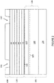
- laser reflective material 128 is formed on an upper surface of the semiconductor body 102 or on top of the passivation layer 126 (if present). Properties of the laser reflective material 128 and techniques for forming the laser reflective material 128 will be described in further detail below.
- a first etch resistant mask 130 is formed on top of the laser reflective material 128.
- the first etch resistant mask 130 can include hardmask materials or photoresist materials.
- the first etch resistant mask 130 is patterned to include first and second openings 132, 134 that expose portions of the laser reflective material 128. This may be done using lithography techniques, for example.
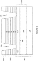
- an etching process is performed.
- the etching process forms first and second openings 136, 138 in the layer of laser reflective material 128, thereby forming a structured laser-reflective mask 140.
- this etching process can include any of a wide variety of semiconductor etching techniques such as wet chemical etching, reactive ion etching, plasma etching, etc.
- the etching process is an anisotropic wet chemical etch process, which results in the first and second openings 136, 138 being tapered.
- the etching process is stopped when the etchant reaches the passivation layer 126.
- the passivation layer 126 remains intact and is exposed at the bottom of the first and second openings 136, 138.
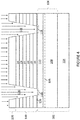
- a dopant implantation process is performed. According to this process, dopant atoms are accelerated towards the upper surface of the semiconductor body 102. The dopant atoms pass through the through the first and second openings 136, 138 in the structured laser-reflective mask 140 and penetrate the passivation layer 126, thereby forming a source contact region 116 and a drain contact region 118 underneath the first and second openings 136, 138. Meanwhile, the structured laser-reflective mask 140 substantially prohibits the dopant atoms from penetrating the semiconductor body 102. That is, the structured laser-reflective mask 140 acts as an ion implantation mask.
- the dopant atoms can include any element that is an impurity with respect to the intrinsic semiconductor material of the semiconductor body 102. These dopant atoms can be used to create p-type or n-type material.
- the dopant atoms are silicon atoms, which form n-type dopants in the type-III semiconductor material.
- a dopant dose of the implanted silicon atoms may in the range of 10 15 - 10 16 dopant atoms/cm -2 , for example.
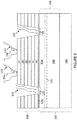
- a laser thermal anneal process is performed. Before performing the laser thermal anneal, the structured laser-reflective mask 140 can be removed, e.g., by an etching technique. Subsequently, the laser thermal anneal process is performed by emitting from a laser source highly concentrated electromagnetic radiation 142 directed towards the semiconductor body 102. Generally speaking, the electromagnetic radiation 142 can be in any frequency range, e.g., infrared, visible spectrum, ultraviolet, etc. In an embodiment, the laser thermal anneal process involves using an excimer laser as the laser source to apply UV radiation with a wavelength of 308 nm.
- the radiation 142 is in the visible light spectrum (i.e., a wavelength of between 400 nm - 700 nm).
- the radiation 142 may be applied in short bursts, e.g., between about 100 ns (nanoseconds) and 200 ns.
- energy from the laser source is substantially transmitted through the first and second openings 136, 138 into the semiconductor body 102.
- a greater amount of energy may be transferred into the semiconductor body 102.
- at least 60%, 70%, 80%, etc., of the energy from the laser source may be transferred through the first and second openings 136, 138 and into the semiconductor body 102 during the laser thermal anneal process.
- the electromagnetic radiation 142 is transmitted through the first and second openings 136, 138 and through the portions of the passivation layer 126 that are exposed by the first and second openings 136, 138.
- the thickness and reflectivity of the passivation layer 126 is such that most of the energy from the laser source passes through the passivation layer 126 and into the semiconductor body 102.
- the laser thermal anneal process locally elevates the temperature of the source and drain contact regions 112, 114 to a dopant activation temperature, e.g., at least 800°C, at least 900°C, etc. As a result, the source and drain contact regions 112, 114 become electrically active doped regions.
- energy from the laser source is substantially reflected by the laser-reflective mask 140.
- at least 60%, 70%, 80%, etc., of the energy from the laser source may be reflected by the laser-reflective mask 140 during the laser thermal anneal process.
- the portions of the semiconductor body 102 that are covered by the laser-reflective mask 140 i.e., the portions of the semiconductor body 102 outside of the source and drain contact regions 112, 114, are substantially cooler during the laser thermal annealing process.
- these regions can remain at a temperature of below e.g., at least 300°C, at least 200°C, etc., while the source and drain contact regions 112, 114 are elevated to the dopant activation temperature.
- the structured laser-reflective mask 140 is removed after performing the laser thermal anneal process. This may be done using a wet chemical etchant, such as an aqueous diluted hydrofluoric acid (DHF). Subsequently, a second etch-resistant mask 148 is provided on top of the passivation layer 126.
- the material of the second etch-resistant mask 148 is configured to permit etching of the passivation layer 126 selective to the mask.
- Exemplary materials for the passivation layer 126 include hardmask materials and photoresist materials.
- the second etch-resistant mask 148 is patterned to include first and second openings 144, 146 directly over the source contact region 116 and the drain contact region 118.
- the passivation layer 126 is etched to include first and second openings 150, 152 that expose the source and drain contact regions 112, 114 in the type III-nitride semiconductor portion 106.
- an electrically conductive material 154 is deposited on the semiconductor body 102. This can be done by a blanket deposition process, e.g., physical vapour deposition (PVD).
- the deposited conductive material 154 fills the first and second openings 150, 152 in the passivation layer 126 and forms an ohmic contact with the source and drain contact regions 112, 114.
- the conductive material 154 can include any of a variety of materials such as nickel, copper, titanium, alloys thereof, metal nitrides, e.g., AIN, TiN, etc.
- the conductive material 154 includes titanium and/or titanium nitride (TiN). After blanket depositing the conductive material 154, it can be structured to remove substantially all of the material that covers the passivation layer 126. This can be done by a selective etching technique, for example.
- a planarization process is performed to remove the remaining conductive material 154 that is present on the passivation layer 126. This may be done using planarization techniques such as chemical mechanical polishing (CMP), grinding, etc. As a result, the source and drain contacts 112, 114 have upper surfaces that are substantially planar and coplanar with the upper surface of the passivation layer 126.
- CMP chemical mechanical polishing
- One advantage of the above described technique is the ability to form a high-quality passivation layer 126 that is protected from harmful processing temperatures.
- the interface between the type III-nitride semiconductor material and the passivation layer 126 plays a significant role in the performance of the device. This interface can become damaged during conventional annealing processes that are used for dopant activation. These annealing processes concurrently heat the passivation layer and damage the interface between the type III-nitride semiconductor material and the passivation layer. Because the above described technique covers the passivation layer 126 with the laser reflective material 128 during the annealing step, the passivation layer 126 remains relatively cool during the laser thermal anneal process.
- the interface between the passivation layer 126 and the semiconductor body 102 is undamaged.
- the technique offers greater flexibility in selecting the size and location of the passivation layer 126, and advantageously allows for the passivation layer 126 to be formed directly over the source and drain contact regions 112, 114 without damage to the interface between the interface between the type III-nitride semiconductor material and the passivation layer 126.
- the above described technique is particularly advantageous in semiconductor substrates that are hybrids of different lattice constant material, for example a type IV semiconductor base material (e.g., Si) with a type III-nitride semiconductor region (e.g., GaN) formed thereon.
- a difference in coefficient of thermal expansion between the hybrid materials results in mechanical stress or strain in the substrate under high temperatures.
- the laser reflective material 128 maintains the temperature of the substrate below values that cause harmful thermal expansion during the laser thermal anneal process.
- the first and second openings 136, 138 in the laser reflective material 128 and the first and second openings 150, 152 in the passivation layer 126 are formed using a single photomask.
- the technique for structuring the passivation layer 126 which determines the geometry of the source and drain contacts 112, 114, is self-aligned with the technique for structuring the laser reflective material 128, which determines the geometry of the source and drain contact regions 112, 114.
- the first etch resistant mask 130 as described with reference to Fig. 2 is lithographically patterned using a first photomask (not shown), and the second etch-resistant mask 148 as described with reference to Fig.
- the second etch-resistant mask 148 as shown in Fig. 6 is omitted, and the structured laser-reflective mask 140 is used directly as an etch mask for forming the first and second openings 150, 152 in the passivation layer 126.
- first and second openings 136, 138 in the laser reflective material 128 and the first and second openings 150, 152 in the passivation layer 126 are formed from separate lithography masks.
- the source and drain contacts 112, 114 are not self-aligned with the source and drain contact regions 112, 114.
- the first etch resistant mask 130 as described with reference to Fig. 2 is lithographically patterned using a first photomask (not shown)
- the second etch-resistant mask 148 as described with reference to Fig. 6 is lithographically patterned using a second photomask (not shown).
- One advantage of this technique is greater flexibility regarding the size and location of the source and drain contacts 112, 114.
- the laser reflective material 128 may include dielectric materials. Specifically, the laser reflective material 128 may have the configuration of a so-called Bragg mirror. In this configuration, the laser reflective material 128 includes multiple dielectric layers with different reflective properties. More generally, the laser reflective material 128 can include any material configuration which substantially reflects ultraviolet radiation, e.g., reflective metals such as copper, gold, silver, etc.
- the laser reflective material 128 includes a plurality of first-type dielectric material layers 154 type arranged alternatingly with a plurality of second-type dielectric material layers 156.
- the first-type dielectric material is different from the second-type dielectric material, and has a different refractive index n.
- the first-type dielectric material layers 154 are oxide layers (e.g., SiO 2 ) and the second-type dielectric material layers 156 are nitride layers (e.g., Si 3 N 4 ).
- the layered stack can be configured to reflect substantially all of the light directed at the laser-reflective mask 140 in the above described manner.
- the optical depth of each layer can be selected to be at or substantially close to 1 ⁇ 4 of the wavelength of the radiation 142 from the laser source.
- the laser-reflective mask 140 includes three of the first-type dielectric material layers 154 and three of the second-type dielectric material layers 156. This arrangement advantageously provides substantial reflection (e.g., about 80% of the laser energy in the case of a 308 nm laser anneal).
- first-type dielectric material layers 154 and second-type dielectric material layers 156 may be selected based on a variety of factors including desired reflection and processing complexity. Additionally or alternatively, embodiments of a Bragg mirror configuration may include further different dielectric material layers (i.e., third-type dielectric material layers, fourth-type dielectric material layers, etc.) and/or dielectric material layers of different thicknesses.
- some or all of the first-type dielectric material layers 154 and the second-type dielectric material layers 156 are formed by a chemical vapour deposition technique or a physical sputtering technique.
- a chemical vapour deposition technique or a physical sputtering technique.
- One advantage of these techniques is that they can create dielectric layers reliably at predictable thicknesses. Hence, these techniques allow for precise tailoring of the optical depth of the layers of the laser-reflective mask 140, and consequently highly efficient reflection by the laser-reflective mask 140.
- a melting point of the dielectric layers from the laser-reflective mask 140 are higher than the temperature that the semiconductor body 102 is heated to during the laser thermal annealing process.
- the Bragg mirror may include silicon nitride layers with melting point of about 1900°C, silicon dioxide layers with a melting point of about 1700°C, and the laser thermal annealing step may bring the semiconductor body to a temperature of about 800°C - 1000°, e.g., for dopant activation.
- the material of the laser-reflective mask 140 can be selected to withstand the process temperatures of the laser thermal annealing to which it is used.
- the laser-reflective mask 140 includes metallic regions (e.g., copper, silver, etc.) this laser-reflective mask 140 can be used in combination with any process that heats the semiconductor body 102 to lower temperatures than the melting point of these metallic regions (e.g., below about 900°C).
- metallic regions e.g., copper, silver, etc.
- the material of the laser-reflective mask 140 has an energy bandgap that is higher than the type III-nitride semiconductor material of the source and drain contact regions 112, 114.
- This arrangement results in the portion of the semiconductor body 102 that receives energy from the laser (e.g., the source and drain contact regions 112, 114 in the above discussed example) absorbing energy with greater efficiency than within the laser-reflective mask 140.
- the first-type dielectric material layers 154 and the second-type dielectric material layers 156 of the laser-reflective mask 140 each have a higher bandgap than the subjacent GaN material.
- the wavelength of the laser thermal anneal is correlated to the energy bandgap of the material being energized.
- the laser thermal anneal is performed such that ⁇ ⁇ 1240/E, wherein E is an energy bandgap of the material being energized by the laser in electron-volts (eV) and ⁇ is a wavelength of the radiation 142 from the laser source in nanometers. Maintaining this relationship ensures a high absorption coefficient in the targeted material.
- a laser thermal anneal process is shown, according to another embodiment.
- the radiation 142 from the laser source is applied at a non-perpendicular angle relative to the semiconductor body 102.
- the laser being is applied to the laser-reflective mask 140 at an incident angle ⁇ , relative to a plane 156 that is perpendicular to the upper surface of the laser-reflective mask 140.
- the incident angle ⁇ is greater than zero degrees and less than 90 degrees.
- the laser is applied at an acute angle relative to the upper surface of the laser-reflective mask 140.
- each of the layers of the laser-reflective mask 140 may have a thickness of ( ⁇ /4 ⁇ ) ⁇ (1-sin2( ⁇ )/ ⁇ 2 ), wherein ⁇ is a wavelength of the laser, and wherein ⁇ is a refractive index of the layer in question.
- the first-type dielectric material layers 154 each have a first thickness based on the refractive index ⁇ of the first-type dielectric material
- the second-type dielectric material layers 156 each have a second thickness based on the refractive index ⁇ of the second-type dielectric material.
- a laser thermal anneal process is shown, according to another embodiment.
- the laser-reflective mask 140 is used to protect a thermosensitive element 158.
- a semiconductor body 102 is provided.
- the semiconductor body 102 may include type III-nitride semiconductor material according to the configuration described with reference to Fig. 1 .
- the semiconductor body 102 may include only type IV semiconductor materials, e.g., silicon (Si) silicon carbide (SiC) or silicon germanium (SiGe).
- Si silicon
- SiC silicon carbide
- SiGe silicon germanium
- thermosensitive element 158 has a critical temperature at which the thermosensitive element 158 is irreparably damaged.
- the thermosensitive element 158 may any component of an active semiconductor device that is susceptible to damage or malfunction at elevated temperatures, e.g., temperatures associated with semiconductor processing.
- the thermosensitive element 158 can include the gate structure of a MOSFET device. More specifically, the thermosensitive element 158 can include electrically conductive gate electrode material (e.g., copper, aluminum, polysilicon, etc.) of a MOSFET device. If heated beyond a critical temperature, e.g., the melting point of the gate electrode material, the structure can become irreversibly damaged.
- the thermosensitive element 158 can include the gate structure of a HEMT device.
- This gate structure may include an electrically conductive gate electrode which is susceptible to damage for the reasons explained above. Additionally, this gate structure can include a region of doped III-nitride semiconductor material that is configured to deplete a two-dimensional charge carrier gas, e.g., as described in the gate structure 120 with reference to Fig. 1 . This region may include p-type dopants (e.g., magnesium) which tend to diffuse out of the material when the device is subjected to high temperatures, e.g., above 800° C. Still other examples of the thermosensitive element 158 include bipolar transistors, e.g., with a SiGe:C base, capacitors, with ferro-electric dielectrics which are unstable at high temperatures.
- p-type dopants e.g., magnesium
- the thermosensitive element 158 include bipolar transistors, e.g., with a SiGe:C base, capacitors, with ferro-electric dielectrics which are unstable at high temperatures.
- thermosensitive element 158 can be any element that shows deconstruction when exposed to thermal budgets beyond a certain threshold.
- the thermosensitive element 158 can be formed on the upper surface of the semiconductor body 102 (e.g., in the case of a planar gate structure 120) or within the semiconductor body 102 (e.g., in the case of a trenched gate structure 120).
- a laser-reflective mask 140 is formed to cover the thermosensitive element 158.
- the laser-reflective mask 140 may include any of the materials previously described and may be formed according to any of the techniques previously described.
- the laser-reflective mask 140 may be formed by initially depositing a blanket layer or layers that completely covers the thermosensitive element 158.
- the laser-reflective mask 140 may be formed by successively depositing the dielectric layers (e.g., by chemical vapor deposition or physical sputtering) directly on the gate electrode 122.
- the upper surface of the laser-reflective mask 140 is planar in the figure, this surface may be undulated due to conformal deposition.
- the material is structured to include first and second openings 136, 138, e.g., according to the previously described techniques.
- laser thermal annealing may be performed.
- radiation 142 is generated by a laser source and transmitted through the first and second openings 136, 138 in the manner previously described.
- the exposed regions of the semiconductor body 102 are heated.
- the portions of the semiconductor body 102 covered by the laser-reflective mask 140 are substantially prevented from receiving the laser energy.
- the regions protected by the laser-reflective mask 140 remain cool.
- the laser thermal annealing process is used in a source/drain dopant activation technique (e.g., as described above, wherein the source and drain regions are locally elevated to a temperature of about 800° C).
- the region that includes the thermosensitive element 158 remains relatively cool, e.g., at or below 300° C.
- the thermosensitive element 158 is advantageously prevented from being exposed to damaging temperature.
- HEMT is also commonly referred to as HFET (heterostructure field effect transistor 100), MODFET (modulation-doped FET) and MESFET (metal semiconductor field effect transistor 100).
- HFET heterostructure field effect transistor 100
- MODFET modulation-doped FET
- MESFET metal semiconductor field effect transistor 100
- HEMT, HFET, MESFET and MODFET are used interchangeably herein to refer to any III-nitride based compound semiconductor transistor 100 incorporating a junction between two materials with different band gaps (i.e., a heterojunction) as the channel.
Landscapes
- Junction Field-Effect Transistors (AREA)
- Physics & Mathematics (AREA)
- Electromagnetism (AREA)
- Optics & Photonics (AREA)
- Chemical & Material Sciences (AREA)
- Engineering & Computer Science (AREA)
- Ceramic Engineering (AREA)
- Recrystallisation Techniques (AREA)
Abstract
Description
- Ion implantation is used to form doped regions in semiconductor devices. According to this technique, impurity atoms are implanted into a semiconductor body by injecting accelerated atoms into the surface of the semiconductor body. After the atoms are implanted, a dopant activation step is performed. The dopant activation step applies heat to the semiconductor body. This thermal energy repairs the crystal damage caused by the atom implantation. Moreover, this thermal energy induces the implanted dopant atoms to move into substitutional lattice sites, thereby producing electrically active donors or acceptors in the semiconductor material. One challenge associated with ion implantation is that the thermal budget required for dopant activation step can damage other components of the semiconductor device.
- According to the invention, a method of forming a semiconductor device comprises providing a semiconductor body comprising a base carrier portion and a type III-nitride semiconductor portion disposed on the base carrier portion, the type III-nitride semiconductor portion comprising a heterojunction and two-dimensional charge carrier gas, forming one or more ohmic contacts in the type III-nitride semiconductor portion, the ohmic contacts forming an ohmic connection with the two-dimensional charge carrier gas, and forming a gate structure that is configured to control a conductive state of the two-dimensional charge carrier gas. Forming the one or more ohmic contacts comprises forming a structured laser-reflective mask on the upper surface of the type III-nitride semiconductor portion, implanting dopant atoms into the upper surface of the type III-nitride semiconductor portion, and performing a laser thermal anneal that activates the implanted dopant atoms.
- In some embodiments, the gate structure is formed before forming the one or more ohmic contacts.
- In some embodiments, forming the structured laser-reflective mask comprises depositing a layer of reflective material on the upper surface of the type III-nitride semiconductor portion and forming first and second openings in the layer of laser reflective material, and wherein the implanting of dopant atoms comprises implanting the dopant atoms through the first and second openings.
- In some embodiments, the reflective material is formed above the gate structure and the first and second openings are positioned on opposing lateral sides of the gate structure.
- In some embodiments, during the laser thermal anneal, the first and second openings substantially transmit energy from the laser into the semiconductor body and the laser-reflective mask substantially reflects energy from the laser.
- In some embodiments, the method further comprises forming an electrically insulating passivation layer on the upper surface of the type III-nitride semiconductor portion, the structured laser-reflective mask is formed on top of the passivation layer, and performing the laser thermal anneal comprises transmitting energy from the laser through the portions of the passivation layer that are exposed by the first and second openings.
- In some embodiments, the passivation layer is positioned directly on peripheral portions of the implanted doped regions of the respective the ohmic contacts formed in the type III-nitride semiconductor portion.
- In some embodiments, the type III-nitride semiconductor portion comprises a channel layer and a barrier layer, the channel layer comprises InXGa(1-X)N, where x≥0, the barrier layer comprises InxAlyGazN, where x≥0, y>0 and z=1-x-y.
- In some embodiments, the passivation layer is a layer of silicon nitride.
- In some embodiments, the method further comprises structuring the passivation layer after performing the laser thermal anneal to include first and second openings in the passivation layer, and depositing electrically conductive material in the first and second openings of the passivation layer to form the one or more ohmic contacts, and the first and second openings in the layer of laser reflective material and the first and second openings in the passivation layer are formed by a common photomask.
- In some embodiments, the method further comprises structuring the passivation layer after performing the laser thermal anneal to include first and second openings in the passivation layer, and depositing electrically conductive material in the first and second openings of the passivation layer to form the one or more ohmic contacts, and the first and second openings in the layer of laser reflective material and the first and second openings in the passivation layer are formed by separate photomasks.
- In some embodiments, after forming the first and second openings, portions of the passivation layer are in direct contact with portions, for example peripheral portions, of the doped regions of the respective one or more ohmic contacts.
- In some embodiments, the one or more ohmic contacts comprise conductive metal regions formed on a surface of the type III-nitride semiconductor portion and doped regions implanted in the type III-nitride portion beneath the conductive metal regions, wherein the conductive metal regions directly cover and contact the implanted doped regions.
- In some embodiments, the conductive metal regions are positioned directly on the electrically insulating passivation layer and directly on the implanted doped regions.
- In some embodiments, the laser-reflective mask comprises a plurality of first-type dielectric material layers arranged alternatingly with a plurality of second-type dielectric material layers, and the first-type dielectric material has a different refractive index as the second-type dielectric material.
- In some embodiments, a melting point of the first-type dielectric material and a melting point of the second-type dielectric material are each greater than an activation temperature that activates the implanted dopant atoms.
- In some embodiments, the first-type dielectric material layers and the second-type dielectric material layers is formed by a chemical vapour deposition technique or a physical sputtering technique.
- In some embodiments, the laser thermal anneal is applied with the laser being applied to the laser-reflective mask at an incident angle θ, and wherein each of the first-type dielectric material layers and the second-type dielectric material layers have a thickness of (λ/4η)·√(1-sin2(θ)/η2), wherein λ is a wavelength of the laser, and wherein η is a refractive index of the first-type dielectric material or second type dielectric material of the respective layer.
- In some embodiments, material of the laser-reflective mask has an energy bandgap that is higher than an energy bandgap of the type III-nitride semiconductor material or materials.
- In some embodiments, the laser thermal anneal is performed such that λ <1240/E, wherein E is an energy bandgap of the type III-nitride semiconductor of the type III-nitride semiconductor portion in electron-volts, and wherein λ is a wavelength of the laser in nanometres.
- According to another embodiment, a method of forming a semiconductor device comprises providing a semiconductor body, forming a thermosensitive element on or within the semiconductor body, forming a structured laser-reflective mask on the upper surface of the semiconductor body that covers the thermosensitive element and comprises first and second openings, and performing a laser thermal annealing process that transmits laser energy through the first and second openings and into the semiconductor body. The thermosensitive element comprises a critical temperature at which the thermosensitive element is irreparably damaged. The laser thermal annealing process brings portions of the semiconductor body that are underneath the first and second openings above the critical temperature. During the laser thermal annealing process, the thermosensitive element remains below the critical temperature.
- In some embodiments, the thermosensitive element is a gate electrode of a MOSFET device.
- In some embodiments, the thermosensitive element is a gate structure of a HEMT device.
- In some embodiments, the thermosensitive element is a gate structure of a HEMT device and the gate structure comprises a region of doped III-nitride semiconductor material.
- In some embodiments, the doped III-nitride semiconductor material is p-doped III-nitride semiconductor material, for example p-doped GaN or p-doped AlyGazN, where y>0 and z=1-y.
- In some embodiments, the method further comprises implanting dopant atoms into the upper surface of the type III-nitride semiconductor portion and performing the laser thermal anneal comprises activating the implanted dopant atoms.
- According to an embodiment, a semiconductor device comprises a semiconductor body comprising a base carrier portion and a type III-nitride semiconductor portion disposed on the base carrier portion, the type III-nitride semiconductor portion comprising a heterojunction and two-dimensional charge carrier gas, one or more ohmic contacts that form an ohmic connection with the two-dimensional charge carrier gas, respectively, an electrically insulating passivation layer formed on the base carrier portion directly over the one or more ohmic contacts, and a gate structure that is configured to control a conductive state of the two-dimensional charge carrier gas.
- In some embodiments, the type III-nitride semiconductor portion comprises a channel layer and a barrier layer, the channel layer comprises InXGa(1-X)N, where x≥0, the barrier layer comprises InxAlyGazN, where x≥0, y>0 and z=1-x-y, and the passivation layer is a layer of silicon nitride.
- In some embodiments, the one or more ohmic contacts comprise conductive metal regions formed on a surface of the type III-nitride semiconductor portion and doped regions implanted in the type III-nitride portion beneath the conductive metal regions, wherein the conductive metal regions directly cover and contact the implanted doped regions.
- In some embodiments, the conductive metal regions are positioned directly on the electrically insulating passivation layer and directly on the implanted doped regions.
- The elements of the drawings are not necessarily to scale relative to each other. Like reference numerals designate corresponding similar parts. The features of the various illustrated embodiments can be combined unless they exclude each other. Embodiments are depicted in the drawings and are detailed in the description which follows.
-
Figure 1 depicts a high-electron mobility transistor, according to an embodiment. -
Figure 2 depicts the formation of laser-reflective material on a semiconductor body, according to an embodiment. -
Figure 3 depicts etching the laser-reflective material to form a structured laser-reflective mask, according to an embodiment. -
Figure 4 depicts implanting dopant atoms through the structured laser-reflective mask and into the semiconductor body, according to an embodiment. -
Figure 5 depicts performing a laser thermal anneal process that transmits laser energy through openings of the structured laser-reflective mask, according to an embodiment. -
Figure 6 depicts removing the structured laser-reflective mask forming a second structured mask over passivation layer, according to an embodiment. -
Figure 7 depicts etching openings in the passivation layer, according to an embodiment. -
Figure 8 depicts forming source and drain contacts in the structured passivation layer, according to an embodiment. -
Figure 9 depicts performing an angled laser thermal anneal process that transmits laser energy through openings of the structured laser-reflective mask, according to an embodiment. -
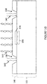
Figure 10 depicts performing a laser thermal anneal process while a thermosensitive element is protected by a laser-reflective mask, according to an embodiment. - Embodiments of a selective laser annealing technique are described herein. The technique advantageously allows for laser annealing of selected regions of a semiconductor body while other portions of the semiconductor body remain cool and unaffected by the laser. According to this technique, laser-reflective material is formed on a semiconductor body. The laser-reflective material is structured, e.g., by etching, to include one or more openings that expose selected portions of the semiconductor body. Subsequently, a laser thermal is performed whereby concentrated radiation is directed towards the semiconductor body. The laser-reflective material of the mask reflects most of the energy from the laser source. Meanwhile, the radiation from the laser source is permitted to pass through the openings in the structured laser-reflective mask. The selective laser thermal anneal technique therefore allows for selective application of energy to designated locations of a semiconductor body, with the adjacent regions that are covered by the laser-reflective mask remaining cool. This advantageously allows for laser thermal annealing to be performed with thermosensitive elements (i.e., features that could be damaged from laser thermal annealing) being present on the semiconductor body.
- Referring to
Fig. 1 , a high-electron mobility transistor 100 is depicted, according to an embodiment. The high-electron mobility transistor 100 is formed in asemiconductor body 102. Thesemiconductor body 102 includes abase portion 104 and a type III-nitride semiconductor portion 106 disposed on thebase portion 104. According to an embodiment, thebase portion 104 includes silicon. For example, thebase portion 104 can be a commercially available bulk silicon wafer. More generally, thebase portion 104 can include any of a wide variety of semiconductor materials, including type IV semiconductor materials, e.g., silicon (Si), sapphire, carbide (SiC), silicon germanium (SiGe), etc. - The type III-
nitride semiconductor portion 106 of thesemiconductor body 102 includes achannel layer 108 and abarrier layer 110 formed on thechannel layer 108. Thebarrier layer 110 and thechannel layer 108 are layers of type III-nitride semiconductor material which have a different bandgap from one another. This difference in bandgap produces a naturally occurring two-dimensional charge carrier gas 105 (i.e., a two-dimensional electron gas (2DEG) or a two-dimensional hole gas (2DHG)) at a heterojunction between thechannel layer 108 and thebarrier layer 110. Generally speaking, thechannel layer 108 and thebarrier layer 110 can include any binary, ternary or quaternary III-V semiconductor materials responsible for this device concept. Examples of these III-V semiconductor materials include gallium arsenide (GaAs), gallium phosphide (GaP), indium phosphide (InP), gallium nitride (GaN), aluminium gallium nitride (AIGaN), indium gallium phosphide (InGaPa) or indium gallium arsenide phosphide (InGaAsP). According to an embodiment, thechannel layer 108 and thebarrier layer 110 are GaN based layers. For example, thechannel layer 108 can be a layer of gallium nitride and thebarrier layer 110 can be layer of aluminum gallium nitride. In another example, thechannel layer 108 can be layer of AlxGa1-xN and thebarrier layer 110 can be a layer of AlyGa1-yN with a higher aluminum concentration as thechannel layer 108. In another example, the channel layer can include InXGa(1-X)N, where x≥0, and the barrier layer can at least partially include InxAlyGazN, where x≥0, y>0 and z=1-x-y. In any of the above examples, the type III-nitride semiconductor portion 106 may include a spacer layer of nitride material (e.g., a 1-2 nm thick layer of AIN) between thechannel layer 108 and thebarrier layer 110. - The
semiconductor body 102 may include further layers or regions (not shown) between thebase portion 104 and thechannel layer 108. For example, thesemiconductor body 102 may include a nucleation layer formed on thebase portion 104 that facilitates epitaxial growth. This nucleation layer can be a thin layer (e.g., a 100-200 nm layer) of AIN (aluminum nitride), for example. Additionally, or alternatively, thesemiconductor body 102 may include additional regions type III-nitride semiconductor material. For example, thesemiconductor body 102 may include a lattice transition region that is configured to alleviate mechanical stress due to lattice mismatch. This lattice transition region may include a layered stack of type III-nitride semiconductor layers of different alloy concentration and/or insulating layers. - The
transistor 100 includes source anddrain contacts nitride semiconductor portion 106. The source anddrain contacts charge carrier gas 105. The source anddrain contacts transistor 100 further includes source and draincontact regions nitride semiconductor portion 106, which provide the ohmic connection between the conductive material of the source anddrain contacts charge carrier gas 105. Thesource contact region 116 is disposed at the interface between thesource contact 112 and the type III-nitride semiconductor portion 106. Likewise, thedrain contact region 118 is disposed at the interface between thedrain contact 114 and the type III-nitride semiconductor portion 106. The source and draincontact regions contact regions nitride semiconductor portion 106 may have a dopant concentration of no more than 5 x 10¹⁵ dopant atoms cm-3. The source and draincontact regions transistor 100 may include any configuration with one or more ohmic contacts which form an ohmic connection with the two-dimensionalcharge carrier gas 105. - The
transistor 100 additionally includes agate structure 120 on the upper surface of the type III-nitride semiconductor portion 106. In a commonly known manner, thegate structure 120 is configured to control a conductive connection between the source anddrain contacts gate structure 120 includes an electricallyconductive gate electrode 122 that receives a gate bias and is configured control the conductive state of the two-dimensionalcharge carrier gas 105. Thegate electrode 122 can include conductive materials such as metals, e.g., nickel, copper, titanium, alloys thereof, metal nitrides, e.g., AIN, TiN, and highly doped semiconductors, e.g., polysilicon. Optionally, thegate structure 120 may include a doped type III-nitride semiconductor region 124 between thegate electrode 122 and the two-dimensionalcharge carrier gas 105. The material properties of the doped type III-nitride semiconductor region 124 (e.g., doping concentration, thickness, etc.) are tailored such that the doped type III-nitride semiconductor region 124 applies an electric field which depletes the two-dimensionalcharge carrier gas 105 in the absence of any external bias to thegate structure 120. Thus, the doped type III-nitride semiconductor region 124 can be used to configure thetransistor 100 as a normally-off device. The doped type III-nitride semiconductor region 124 may be formed from p-doped III-nitride semiconductor material, for example p-doped GaN or p-doped AlyGazN, where y>0 and z=1-y. - The high-
electron mobility transistor 100 additionally includes apassivation layer 126 formed on the upper surface of the type III-nitride semiconductor portion 106. Thepassivation layer 126 includes an electrically insulating material, such as silicon nitride (SiN), silicon dioxide (SiO2), and silicon oxynitride (SiOxNY), to name a few. Thepassivation layer 126 can be a relatively thin (e.g., equal to or less than 100 nm thick, 75 nm thick, 50 nm thick, etc.) layer. Among other things, thepassivation layer 126 protects thesemiconductor body 102 from harmful environmental conditions, including moisture and particulates. - The
passivation layer 126 may be positioned on the peripheral regions of the source and draincontact regions nitride semiconductor portion 106. Thepassivation layer 126 extends between thesource contact 112 and thegate structure 120 and between thegate structure 120 and thedrain contact 112 on the upper surface of the type III-nitride semiconductor portion 106. In some embodiments, the peripheral region of the source anddrain contacts passivation layer 126. - Referring to
Figures 2 - 8 , selected process steps for forming the high-electron mobility transistor 100 are depicted. These process steps may be combined with other known techniques to form the high-electron mobility transistor 100 according to any of the embodiments described above. - Referring to
Figure 2 , asemiconductor body 102 is provided. Thesemiconductor body 102 can have any of the material configurations previously discussed with reference toFig. 1 . According to one technique, thebase portion 104 is provided from a bulk semiconductor wafer, and the various layers of the type III-nitride semiconductor portion 106 including thechannel layer 108 and thebarrier layer 110 are formed by epitaxial deposition. Thepassivation layer 126 may be formed by a deposition process, e.g., chemical vapour deposition (CVD). - After providing the
semiconductor body 102, laserreflective material 128 is formed on an upper surface of thesemiconductor body 102 or on top of the passivation layer 126 (if present). Properties of the laserreflective material 128 and techniques for forming the laserreflective material 128 will be described in further detail below. A first etchresistant mask 130 is formed on top of the laserreflective material 128. The first etchresistant mask 130 can include hardmask materials or photoresist materials. The first etchresistant mask 130 is patterned to include first andsecond openings reflective material 128. This may be done using lithography techniques, for example. - Referring to
Figure 3 , an etching process is performed. The etching process forms first andsecond openings reflective material 128, thereby forming a structured laser-reflective mask 140. Generally speaking, this etching process can include any of a wide variety of semiconductor etching techniques such as wet chemical etching, reactive ion etching, plasma etching, etc. According to an embodiment, the etching process is an anisotropic wet chemical etch process, which results in the first andsecond openings - According to an embodiment, the etching process is stopped when the etchant reaches the
passivation layer 126. As a result, thepassivation layer 126 remains intact and is exposed at the bottom of the first andsecond openings - Referring to
Figure 4 , a dopant implantation process is performed. According to this process, dopant atoms are accelerated towards the upper surface of thesemiconductor body 102. The dopant atoms pass through the through the first andsecond openings reflective mask 140 and penetrate thepassivation layer 126, thereby forming asource contact region 116 and adrain contact region 118 underneath the first andsecond openings reflective mask 140 substantially prohibits the dopant atoms from penetrating thesemiconductor body 102. That is, the structured laser-reflective mask 140 acts as an ion implantation mask. - Generally speaking, the dopant atoms can include any element that is an impurity with respect to the intrinsic semiconductor material of the
semiconductor body 102. These dopant atoms can be used to create p-type or n-type material. In an embodiment, the dopant atoms are silicon atoms, which form n-type dopants in the type-III semiconductor material. A dopant dose of the implanted silicon atoms may in the range of 1015 - 1016 dopant atoms/cm-2, for example. - Referring to
Figure 5 , a laser thermal anneal process is performed. Before performing the laser thermal anneal, the structured laser-reflective mask 140 can be removed, e.g., by an etching technique. Subsequently, the laser thermal anneal process is performed by emitting from a laser source highly concentratedelectromagnetic radiation 142 directed towards thesemiconductor body 102. Generally speaking, theelectromagnetic radiation 142 can be in any frequency range, e.g., infrared, visible spectrum, ultraviolet, etc. In an embodiment, the laser thermal anneal process involves using an excimer laser as the laser source to apply UV radiation with a wavelength of 308 nm. In another embodiment, theradiation 142 is in the visible light spectrum (i.e., a wavelength of between 400 nm - 700 nm). Theradiation 142 may be applied in short bursts, e.g., between about 100 ns (nanoseconds) and 200 ns. - During the laser thermal anneal process, energy from the laser source is substantially transmitted through the first and
second openings semiconductor body 102. This means that at least 50% of the energy from the laser source is transferred into thesemiconductor body 102 in the regions directly underneath the first andsecond openings semiconductor body 102. For example, at least 60%, 70%, 80%, etc., of the energy from the laser source may be transferred through the first andsecond openings semiconductor body 102 during the laser thermal anneal process. Theelectromagnetic radiation 142 is transmitted through the first andsecond openings passivation layer 126 that are exposed by the first andsecond openings passivation layer 126 is such that most of the energy from the laser source passes through thepassivation layer 126 and into thesemiconductor body 102. The laser thermal anneal process locally elevates the temperature of the source and draincontact regions contact regions - Also during the laser thermal anneal process, energy from the laser source is substantially reflected by the laser-
reflective mask 140. This means that greater than 50% of the energy from the laser source is reflected by the laser-reflective mask 140, and hence less than 50% of the energy from the laser source is transmitted to the portions of thesemiconductor body 102 that are underneath the laser-reflective mask 140. For example, at least 60%, 70%, 80%, etc., of the energy from the laser source may be reflected by the laser-reflective mask 140 during the laser thermal anneal process. As a result, the portions of thesemiconductor body 102 that are covered by the laser-reflective mask 140, i.e., the portions of thesemiconductor body 102 outside of the source and draincontact regions contact regions - Referring to
Fig. 6 , the structured laser-reflective mask 140 is removed after performing the laser thermal anneal process. This may be done using a wet chemical etchant, such as an aqueous diluted hydrofluoric acid (DHF). Subsequently, a second etch-resistant mask 148 is provided on top of thepassivation layer 126. The material of the second etch-resistant mask 148 is configured to permit etching of thepassivation layer 126 selective to the mask. Exemplary materials for thepassivation layer 126 include hardmask materials and photoresist materials. The second etch-resistant mask 148 is patterned to include first andsecond openings source contact region 116 and thedrain contact region 118. This may be done using photolithography techniques, for example. Subsequently, thepassivation layer 126 is etched to include first andsecond openings contact regions nitride semiconductor portion 106. - Referring to
Fig. 7 , an electricallyconductive material 154 is deposited on thesemiconductor body 102. This can be done by a blanket deposition process, e.g., physical vapour deposition (PVD). The depositedconductive material 154 fills the first andsecond openings passivation layer 126 and forms an ohmic contact with the source and draincontact regions conductive material 154 can include any of a variety of materials such as nickel, copper, titanium, alloys thereof, metal nitrides, e.g., AIN, TiN, etc. In a particular embodiment, theconductive material 154 includes titanium and/or titanium nitride (TiN). After blanket depositing theconductive material 154, it can be structured to remove substantially all of the material that covers thepassivation layer 126. This can be done by a selective etching technique, for example. - Referring to
Fig. 8 , a planarization process is performed to remove the remainingconductive material 154 that is present on thepassivation layer 126. This may be done using planarization techniques such as chemical mechanical polishing (CMP), grinding, etc. As a result, the source anddrain contacts passivation layer 126. - One advantage of the above described technique is the ability to form a high-
quality passivation layer 126 that is protected from harmful processing temperatures. In type III-nitride semiconductor devices, the interface between the type III-nitride semiconductor material and thepassivation layer 126 plays a significant role in the performance of the device. This interface can become damaged during conventional annealing processes that are used for dopant activation. These annealing processes concurrently heat the passivation layer and damage the interface between the type III-nitride semiconductor material and the passivation layer. Because the above described technique covers thepassivation layer 126 with the laserreflective material 128 during the annealing step, thepassivation layer 126 remains relatively cool during the laser thermal anneal process. Hence, the interface between thepassivation layer 126 and thesemiconductor body 102 is undamaged. Hence, the technique offers greater flexibility in selecting the size and location of thepassivation layer 126, and advantageously allows for thepassivation layer 126 to be formed directly over the source and draincontact regions passivation layer 126. The above described technique is particularly advantageous in semiconductor substrates that are hybrids of different lattice constant material, for example a type IV semiconductor base material (e.g., Si) with a type III-nitride semiconductor region (e.g., GaN) formed thereon. In that case, a difference in coefficient of thermal expansion between the hybrid materials results in mechanical stress or strain in the substrate under high temperatures. The laserreflective material 128 maintains the temperature of the substrate below values that cause harmful thermal expansion during the laser thermal anneal process. - In one embodiment of the above described technique, the first and
second openings reflective material 128 and the first andsecond openings passivation layer 126 are formed using a single photomask. Hence, the technique for structuring thepassivation layer 126, which determines the geometry of the source anddrain contacts reflective material 128, which determines the geometry of the source and draincontact regions resistant mask 130 as described with reference toFig. 2 is lithographically patterned using a first photomask (not shown), and the second etch-resistant mask 148 as described with reference toFig. 6 is lithographically patterned using the first photomask again. According to another example of a self-aligned technique, the second etch-resistant mask 148 as shown inFig. 6 is omitted, and the structured laser-reflective mask 140 is used directly as an etch mask for forming the first andsecond openings passivation layer 126. These self-aligned techniques advantageously mitigate process cost and complexity. - In another embodiment the first and
second openings reflective material 128 and the first andsecond openings passivation layer 126 are formed from separate lithography masks. Hence, the source anddrain contacts contact regions resistant mask 130 as described with reference toFig. 2 is lithographically patterned using a first photomask (not shown), and the second etch-resistant mask 148 as described with reference toFig. 6 is lithographically patterned using a second photomask (not shown). One advantage of this technique is greater flexibility regarding the size and location of the source anddrain contacts - Various techniques for forming the laser-
reflective mask 140 will now be discussed. In an embodiment, the laserreflective material 128 may include dielectric materials. Specifically, the laserreflective material 128 may have the configuration of a so-called Bragg mirror. In this configuration, the laserreflective material 128 includes multiple dielectric layers with different reflective properties. More generally, the laserreflective material 128 can include any material configuration which substantially reflects ultraviolet radiation, e.g., reflective metals such as copper, gold, silver, etc. - Referring again to
Fig. 3 , one example of a laser-reflective mask 140 with a Bragg mirror configuration is shown. In this embodiment, the laserreflective material 128 includes a plurality of first-type dielectric material layers 154 type arranged alternatingly with a plurality of second-type dielectric material layers 156. The first-type dielectric material is different from the second-type dielectric material, and has a different refractive index n. In one example, the first-type dielectric material layers 154 are oxide layers (e.g., SiO2) and the second-type dielectric material layers 156 are nitride layers (e.g., Si3N4). By appropriately tailoring the thickness of the dielectric material layers with respect to a given radiation wavelength, the layered stack can be configured to reflect substantially all of the light directed at the laser-reflective mask 140 in the above described manner. Specifically, the optical depth of each layer can be selected to be at or substantially close to ¼ of the wavelength of theradiation 142 from the laser source. In the depicted embodiment, the laser-reflective mask 140 includes three of the first-type dielectric material layers 154 and three of the second-type dielectric material layers 156. This arrangement advantageously provides substantial reflection (e.g., about 80% of the laser energy in the case of a 308 nm laser anneal). More generally, the number of first-type dielectric material layers 154 and second-type dielectric material layers 156 may be selected based on a variety of factors including desired reflection and processing complexity. Additionally or alternatively, embodiments of a Bragg mirror configuration may include further different dielectric material layers (i.e., third-type dielectric material layers, fourth-type dielectric material layers, etc.) and/or dielectric material layers of different thicknesses. - According to an embodiment, some or all of the first-type dielectric material layers 154 and the second-type dielectric material layers 156 are formed by a chemical vapour deposition technique or a physical sputtering technique. One advantage of these techniques is that they can create dielectric layers reliably at predictable thicknesses. Hence, these techniques allow for precise tailoring of the optical depth of the layers of the laser-
reflective mask 140, and consequently highly efficient reflection by the laser-reflective mask 140. - According to an embodiment, a melting point of the dielectric layers from the laser-
reflective mask 140 are higher than the temperature that thesemiconductor body 102 is heated to during the laser thermal annealing process. For example, the Bragg mirror may include silicon nitride layers with melting point of about 1900°C, silicon dioxide layers with a melting point of about 1700°C, and the laser thermal annealing step may bring the semiconductor body to a temperature of about 800°C - 1000°, e.g., for dopant activation. More generally, the material of the laser-reflective mask 140 can be selected to withstand the process temperatures of the laser thermal annealing to which it is used. If, for example, the laser-reflective mask 140 includes metallic regions (e.g., copper, silver, etc.) this laser-reflective mask 140 can be used in combination with any process that heats thesemiconductor body 102 to lower temperatures than the melting point of these metallic regions (e.g., below about 900°C). - According to an embodiment, the material of the laser-
reflective mask 140 has an energy bandgap that is higher than the type III-nitride semiconductor material of the source and draincontact regions semiconductor body 102 that receives energy from the laser (e.g., the source and draincontact regions reflective mask 140. For example, in the above described Bragg mirror configuration, the first-type dielectric material layers 154 and the second-type dielectric material layers 156 of the laser-reflective mask 140 each have a higher bandgap than the subjacent GaN material. - According to an embodiment, the wavelength of the laser thermal anneal is correlated to the energy bandgap of the material being energized. In an example of this concept, the laser thermal anneal is performed such that λ <1240/E, wherein E is an energy bandgap of the material being energized by the laser in electron-volts (eV) and λ is a wavelength of the
radiation 142 from the laser source in nanometers. Maintaining this relationship ensures a high absorption coefficient in the targeted material. - Referring to
Fig. 9 , a laser thermal anneal process is shown, according to another embodiment. According to this technique, theradiation 142 from the laser source is applied at a non-perpendicular angle relative to thesemiconductor body 102. In more detail, the laser being is applied to the laser-reflective mask 140 at an incident angle θ, relative to aplane 156 that is perpendicular to the upper surface of the laser-reflective mask 140. The incident angle θ is greater than zero degrees and less than 90 degrees. Hence, the laser is applied at an acute angle relative to the upper surface of the laser-reflective mask 140. - According to an embodiment, the properties of the laser-
reflective mask 140 are tailored to maximize reflectivity for the angled laser technique. In more detail, each of the layers of the laser-reflective mask 140 (i.e., the first-type dielectric material layers 154 and the second-type dielectric material layers 156) may have a thickness of (λ/4η)·√(1-sin2(θ)/η2), wherein λ is a wavelength of the laser, and wherein η is a refractive index of the layer in question. Hence, the first-type dielectric material layers 154 each have a first thickness based on the refractive index η of the first-type dielectric material, and the second-type dielectric material layers 156 each have a second thickness based on the refractive index η of the second-type dielectric material. By selecting thickness of the layers in the laser-reflective mask 140 to conform to this requirement, the laser-reflective mask 140 is well-suited to reflect substantially all of the laser energy, e.g., at least 80% of the laser energy. - Referring to
Fig. 10 , a laser thermal anneal process is shown, according to another embodiment. In this embodiment, the laser-reflective mask 140 is used to protect athermosensitive element 158. According to this technique, asemiconductor body 102 is provided. Thesemiconductor body 102 may include type III-nitride semiconductor material according to the configuration described with reference toFig. 1 . Alternatively, thesemiconductor body 102 may include only type IV semiconductor materials, e.g., silicon (Si) silicon carbide (SiC) or silicon germanium (SiGe). Before the laser thermal anneal process is performed, at least onethermosensitive element 158 is formed on or in thesemiconductor body 102. Thethermosensitive element 158 has a critical temperature at which thethermosensitive element 158 is irreparably damaged. Generally speaking, thethermosensitive element 158 may any component of an active semiconductor device that is susceptible to damage or malfunction at elevated temperatures, e.g., temperatures associated with semiconductor processing. For example, thethermosensitive element 158 can include the gate structure of a MOSFET device. More specifically, thethermosensitive element 158 can include electrically conductive gate electrode material (e.g., copper, aluminum, polysilicon, etc.) of a MOSFET device. If heated beyond a critical temperature, e.g., the melting point of the gate electrode material, the structure can become irreversibly damaged. In another example, thethermosensitive element 158 can include the gate structure of a HEMT device. This gate structure may include an electrically conductive gate electrode which is susceptible to damage for the reasons explained above. Additionally, this gate structure can include a region of doped III-nitride semiconductor material that is configured to deplete a two-dimensional charge carrier gas, e.g., as described in thegate structure 120 with reference toFig. 1 . This region may include p-type dopants (e.g., magnesium) which tend to diffuse out of the material when the device is subjected to high temperatures, e.g., above 800° C. Still other examples of thethermosensitive element 158 include bipolar transistors, e.g., with a SiGe:C base, capacitors, with ferro-electric dielectrics which are unstable at high temperatures. More generally, thethermosensitive element 158 can be any element that shows deconstruction when exposed to thermal budgets beyond a certain threshold. Thethermosensitive element 158 can be formed on the upper surface of the semiconductor body 102 (e.g., in the case of a planar gate structure 120) or within the semiconductor body 102 (e.g., in the case of a trenched gate structure 120). - A laser-
reflective mask 140 is formed to cover thethermosensitive element 158. The laser-reflective mask 140 may include any of the materials previously described and may be formed according to any of the techniques previously described. The laser-reflective mask 140 may be formed by initially depositing a blanket layer or layers that completely covers thethermosensitive element 158. For example, in the case that the device structure is ametal gate electrode 122, the laser-reflective mask 140 may be formed by successively depositing the dielectric layers (e.g., by chemical vapor deposition or physical sputtering) directly on thegate electrode 122. Although the upper surface of the laser-reflective mask 140 is planar in the figure, this surface may be undulated due to conformal deposition. Subsequently, the material is structured to include first andsecond openings - After structuring the laser-
reflective mask 140, laser thermal annealing may be performed. During this process,radiation 142 is generated by a laser source and transmitted through the first andsecond openings semiconductor body 102 are heated. Meanwhile, the portions of thesemiconductor body 102 covered by the laser-reflective mask 140 are substantially prevented from receiving the laser energy. Thus, the regions protected by the laser-reflective mask 140 remain cool. In one example of this concept, the laser thermal annealing process is used in a source/drain dopant activation technique (e.g., as described above, wherein the source and drain regions are locally elevated to a temperature of about 800° C). Meanwhile, the region that includes thethermosensitive element 158 remains relatively cool, e.g., at or below 300° C. Thus, thethermosensitive element 158 is advantageously prevented from being exposed to damaging temperature. - The term HEMT is also commonly referred to as HFET (heterostructure field effect transistor 100), MODFET (modulation-doped FET) and MESFET (metal semiconductor field effect transistor 100). The terms HEMT, HFET, MESFET and MODFET are used interchangeably herein to refer to any III-nitride based
compound semiconductor transistor 100 incorporating a junction between two materials with different band gaps (i.e., a heterojunction) as the channel. - As used herein, the terms "having," "containing," "including," "comprising" and the like are open-ended terms that indicate the presence of stated elements or features, but do not preclude additional elements or features. The articles "a," "an" and "the" are intended to include the plural as well as the singular, unless the context clearly indicates otherwise.
- It is to be understood that the features of the various embodiments described herein may be combined with each other, unless specifically noted otherwise.
- Although specific embodiments have been illustrated and described herein, it will be appreciated by those of ordinary skill in the art that a variety of alternate and/or equivalent implementations may be substituted for the specific embodiments shown and described without departing from the scope of the present invention. This application is intended to cover any adaptations or variations of the specific embodiments discussed herein. Therefore, it is intended that this invention be limited only by the claims and the equivalents thereof.
Claims (15)
- A method of forming a semiconductor device, the method comprising:providing a semiconductor body comprising a base carrier portion and a type III-nitride semiconductor portion disposed on the base carrier portion, the type III-nitride semiconductor portion comprising a heterojunction and two-dimensional charge carrier gas;forming one or more ohmic contacts in the type III-nitride semiconductor portion, the ohmic contacts forming an ohmic connection with the two-dimensional charge carrier gas; andforming a gate structure that is configured to control a conductive state of the two-dimensional charge carrier gas;wherein forming the one or more ohmic contacts comprises:forming a structured laser-reflective mask on the upper surface of the type III-nitride semiconductor portion;implanting dopant atoms into the upper surface of the type III-nitride semiconductor portion; andperforming a laser thermal anneal that activates the implanted dopant atoms.
- The method of claim 1, wherein forming the structured laser-reflective mask comprises depositing a layer of reflective material on the upper surface of the type III-nitride semiconductor portion and forming first and second openings in the layer of laser reflective material, and wherein the implanting of dopant atoms comprises implanting the dopant atoms through the first and second openings.
- The method of claim 1 or claim 2, further comprising forming an electrically insulating passivation layer on the upper surface of the type III-nitride semiconductor portion, wherein the structured laser-reflective mask is formed on top of the passivation layer, and wherein performing the laser thermal anneal comprises transmitting energy from the laser through the portions of the passivation layer that are exposed by the first and second openings.
- The method of claim 3, wherein the type III-nitride semiconductor portion comprises a channel layer and a barrier layer, wherein the channel layer comprises InXGa(1-X)N, where x≥0, wherein the barrier layer comprises InxAlyGazN, where x≥0, y>0 and z=1-x-y, and wherein the passivation layer is a layer of silicon nitride.
- The method of claim 3, further comprising:structuring the passivation layer after performing the laser thermal anneal to include first and second openings in the passivation layer; anddepositing electrically conductive material in the first and second openings in the passivation layer to form the one or more ohmic contacts, andwherein the first and second openings in the layer of laser reflective material and the first and second openings in the passivation layer are formed by a common photomask, or, by separate photomasks.
- The method of any one of claims 1 to 5, wherein the laser-reflective mask comprises a plurality of first-type dielectric material layers type arranged alternatingly with a plurality of second-type dielectric material layers, and wherein the first-type dielectric material has a different refractive index as the second-type dielectric material.
- The method of claim 6, wherein at least one of the first-type dielectric material layers and the second-type dielectric material layers is formed by a chemical vapour deposition technique or a physical sputtering technique.
- The method of claim 6 or claim 7, wherein the laser thermal anneal is applied with the laser being applied to the laser-reflective mask at an incident angle θ, and wherein each of the first-type dielectric material layers and the second-type dielectric material layers have a thickness of (λ/4η)·√(1-sin2(θ)/η2), wherein λ is a wavelength of the laser, and wherein η is a refractive index of the first-type dielectric material or second type dielectric material of the respective layer.
- The method of any one of claims 1 to 8, wherein the material of the laser-reflective mask has an energy bandgap that is higher than an energy bandgap of the type III-nitride semiconductor material.
- The method of any one of claims 1 to 9, wherein the laser thermal anneal is performed such that λ <1240/E, wherein E is an energy bandgap of the type III-nitride semiconductor of the type III-nitride semiconductor portion in electron-volts, and wherein λ is a wavelength of the light in nanometres.
- A method of forming a semiconductor device, the method comprising:providing a semiconductor body;forming a thermosensitive element on or within the semiconductor body,forming a structured laser-reflective mask on the upper surface of the semiconductor body that covers the thermosensitive element and comprises first and second openings; andperforming a laser thermal annealing process that transmits laser energy through the first and second openings and into the semiconductor body,wherein the thermosensitive element comprises a critical temperature at which the thermosensitive element irreparably damaged,wherein the laser thermal annealing process brings portions of the semiconductor body that are underneath the first and second openings to above the critical temperature, andwherein during the laser thermal annealing process the thermosensitive element remains below the critical temperature.
- The method of claim 11, wherein the thermosensitive element is a gate electrode of a MOSFET device, or wherein the thermosensitive element is a gate structure of a HEMT device, and wherein the gate structure comprises a region of doped III-nitride semiconductor material.
- The method of claim 11 or claim 12, further comprising implanting dopant atoms into the upper surface of the semiconductor body, and wherein performing the laser thermal anneal comprises activating the implanted dopant atoms.
- A semiconductor device, comprising:a semiconductor body comprising a base carrier portion and a type III-nitride semiconductor portion disposed on the base carrier portion, the type III-nitride semiconductor portion comprising a heterojunction and two-dimensional charge carrier gas;one or more ohmic contacts that form an ohmic connection with the two-dimensional charge carrier gas;an electrically insulating passivation layer formed on the base carrier portion directly over the one or more ohmic contacts; anda gate structure that is configured to control a conductive state of the two-dimensional charge carrier gas.
- The semiconductor device of claim 14, wherein the one or more ohmic contacts comprise conductive metal regions formed on a surface of the type III-nitride semiconductor portion and doped regions implanted in the type III-nitride portion beneath the conductive metal regions, wherein the conductive metal regions directly cover and contact the implanted doped regions.
Applications Claiming Priority (1)
| Application Number | Priority Date | Filing Date | Title |
|---|---|---|---|
| US16/894,223 US11581418B2 (en) | 2020-06-05 | 2020-06-05 | Selective thermal annealing method |
Publications (2)
| Publication Number | Publication Date |
|---|---|
| EP3920236A2 true EP3920236A2 (en) | 2021-12-08 |
| EP3920236A3 EP3920236A3 (en) | 2022-04-20 |
Family
ID=76217653
Family Applications (1)
| Application Number | Title | Priority Date | Filing Date |
|---|---|---|---|
| EP21176603.5A Pending EP3920236A3 (en) | 2020-06-05 | 2021-05-28 | Selective laser annealing method |
Country Status (4)
| Country | Link |
|---|---|
| US (3) | US11581418B2 (en) |
| EP (1) | EP3920236A3 (en) |
| KR (1) | KR20210152388A (en) |
| CN (1) | CN113764265A (en) |
Families Citing this family (3)
| Publication number | Priority date | Publication date | Assignee | Title |
|---|---|---|---|---|
| CN117954321A (en) * | 2024-03-26 | 2024-04-30 | 山东大学 | A gallium nitride HEMT based on laser annealing process and preparation method thereof |
| DE102024124978B4 (en) | 2024-09-02 | 2026-03-26 | Fraunhofer-Gesellschaft zur Förderung der angewandten Forschung eingetragener Verein | Method for producing structured metallic contacts on a semiconductor substrate |
| CN119767726A (en) * | 2024-12-31 | 2025-04-04 | 广东省科学院半导体研究所 | Gallium nitride device preparation method and gallium nitride device |
Family Cites Families (9)
| Publication number | Priority date | Publication date | Assignee | Title |
|---|---|---|---|---|
| US6514840B2 (en) * | 1999-04-13 | 2003-02-04 | International Business Machines Corporation | Micro heating of selective regions |
| JP4986415B2 (en) * | 2004-06-14 | 2012-07-25 | 株式会社半導体エネルギー研究所 | Method for manufacturing semiconductor device |
| EP1791173A1 (en) | 2005-11-25 | 2007-05-30 | STMicroelectronics S.r.l. | Process for manufacturing a MOSFET and corresponding MOSFET |
| US7622374B2 (en) | 2005-12-29 | 2009-11-24 | Infineon Technologies Ag | Method of fabricating an integrated circuit |
| US7494857B2 (en) * | 2006-12-29 | 2009-02-24 | Taiwan Semiconductor Manufacturing Company, Ltd. | Advanced activation approach for MOS devices |
| WO2010008383A1 (en) * | 2008-07-16 | 2010-01-21 | Sionyx, Inc. | Thin sacrificial masking films for protecting semiconductors from pulsed laser process |
| US8216924B2 (en) | 2009-10-16 | 2012-07-10 | Cree, Inc. | Methods of fabricating transistors using laser annealing of source/drain regions |
| FR3026559B1 (en) | 2014-09-30 | 2017-12-22 | Commissariat Energie Atomique | LOCALIZED ANNEALING METHOD OF SEMICONDUCTOR ELEMENTS USING REFLECTOR AREA |
| JPWO2017163356A1 (en) * | 2016-03-24 | 2019-01-31 | 国立大学法人九州大学 | Laser doping apparatus and semiconductor device manufacturing method |
-
2020
- 2020-06-05 US US16/894,223 patent/US11581418B2/en active Active
-
2021
- 2021-05-28 EP EP21176603.5A patent/EP3920236A3/en active Pending
- 2021-06-01 KR KR1020210070515A patent/KR20210152388A/en not_active Ceased
- 2021-06-04 CN CN202110623979.8A patent/CN113764265A/en active Pending
-
2023
- 2023-01-05 US US18/093,434 patent/US12278275B2/en active Active
-
2025
- 2025-04-14 US US19/178,169 patent/US20250240993A1/en active Pending
Also Published As
| Publication number | Publication date |
|---|---|
| US20210384318A1 (en) | 2021-12-09 |
| US20250240993A1 (en) | 2025-07-24 |
| EP3920236A3 (en) | 2022-04-20 |
| US12278275B2 (en) | 2025-04-15 |
| CN113764265A (en) | 2021-12-07 |
| KR20210152388A (en) | 2021-12-15 |
| US20230155000A1 (en) | 2023-05-18 |
| US11581418B2 (en) | 2023-02-14 |
Similar Documents
| Publication | Publication Date | Title |
|---|---|---|
| EP3734666B1 (en) | Semiconductor device and fabrication method thereof | |
| US12278275B2 (en) | Selective laser annealing method | |
| US10790375B2 (en) | High electron mobility transistor | |
| US9236464B2 (en) | Method of forming a high electron mobility transistor | |
| US8105889B2 (en) | Methods of fabricating transistors including self-aligned gate electrodes and source/drain regions | |
| US11527606B2 (en) | Semiconductor device and method for forming the same | |
| KR101991036B1 (en) | ION IMPLANTED AND SELF ALIGNED GATE STRUCTURE FOR GaN TRANSISTORS | |
| US20230387289A1 (en) | Vertical field effect transistor device and method of fabrication | |
| CN107452684B (en) | Method for enhancing surface doping concentration of source/drain region | |
| US9691878B2 (en) | Method of manufacturing MOSFET | |
| US9917187B2 (en) | Semiconductor device and manufacturing method | |
| US8697505B2 (en) | Method of forming a semiconductor structure | |
| EP4213216A1 (en) | High electron mobility transistor and methods for fabricating the same | |
| US12243935B2 (en) | High electron mobility transistor devices having a silicided polysilicon layer | |
| US20240014307A1 (en) | High electron mobility transistor (hemt) device and method of forming the same | |
| US12051739B2 (en) | Package structure having a first connection circuit and manufacturing method thereof | |
| US20250006831A1 (en) | Semiconductor device and method for forming the same | |
| CN113540228A (en) | semiconductor device |
Legal Events
| Date | Code | Title | Description |
|---|---|---|---|
| PUAI | Public reference made under article 153(3) epc to a published international application that has entered the european phase |
Free format text: ORIGINAL CODE: 0009012 |
|
| STAA | Information on the status of an ep patent application or granted ep patent |
Free format text: STATUS: THE APPLICATION HAS BEEN PUBLISHED |
|
| AK | Designated contracting states |
Kind code of ref document: A2 Designated state(s): AL AT BE BG CH CY CZ DE DK EE ES FI FR GB GR HR HU IE IS IT LI LT LU LV MC MK MT NL NO PL PT RO RS SE SI SK SM TR |
|
| PUAL | Search report despatched |
Free format text: ORIGINAL CODE: 0009013 |
|
| AK | Designated contracting states |
Kind code of ref document: A3 Designated state(s): AL AT BE BG CH CY CZ DE DK EE ES FI FR GB GR HR HU IE IS IT LI LT LU LV MC MK MT NL NO PL PT RO RS SE SI SK SM TR |
|
| RIC1 | Information provided on ipc code assigned before grant |
Ipc: H01L 29/20 20060101ALN20220315BHEP Ipc: H01L 29/10 20060101ALN20220315BHEP Ipc: H01L 29/08 20060101ALN20220315BHEP Ipc: H01L 21/265 20060101ALN20220315BHEP Ipc: H01L 21/285 20060101ALI20220315BHEP Ipc: H01L 21/268 20060101ALI20220315BHEP Ipc: H01L 21/337 20060101ALI20220315BHEP Ipc: H01L 29/778 20060101AFI20220315BHEP |
|
| STAA | Information on the status of an ep patent application or granted ep patent |
Free format text: STATUS: REQUEST FOR EXAMINATION WAS MADE |
|
| 17P | Request for examination filed |
Effective date: 20221020 |
|
| RBV | Designated contracting states (corrected) |
Designated state(s): AL AT BE BG CH CY CZ DE DK EE ES FI FR GB GR HR HU IE IS IT LI LT LU LV MC MK MT NL NO PL PT RO RS SE SI SK SM TR |