EP3920223A1 - Storage structure and method for forming same - Google Patents
Storage structure and method for forming same Download PDFInfo
- Publication number
- EP3920223A1 EP3920223A1 EP19932107.6A EP19932107A EP3920223A1 EP 3920223 A1 EP3920223 A1 EP 3920223A1 EP 19932107 A EP19932107 A EP 19932107A EP 3920223 A1 EP3920223 A1 EP 3920223A1
- Authority
- EP
- European Patent Office
- Prior art keywords
- groove
- trench
- dielectric layer
- insulating layer
- grooves
- Prior art date
- Legal status (The legal status is an assumption and is not a legal conclusion. Google has not performed a legal analysis and makes no representation as to the accuracy of the status listed.)
- Granted
Links
Images






Classifications
-
- H—ELECTRICITY
- H10—SEMICONDUCTOR DEVICES; ELECTRIC SOLID-STATE DEVICES NOT OTHERWISE PROVIDED FOR
- H10B—ELECTRONIC MEMORY DEVICES
- H10B12/00—Dynamic random access memory [DRAM] devices
- H10B12/01—Manufacture or treatment
- H10B12/02—Manufacture or treatment for one transistor one-capacitor [1T-1C] memory cells
- H10B12/05—Making the transistor
- H10B12/056—Making the transistor the transistor being a FinFET
-
- H—ELECTRICITY
- H10—SEMICONDUCTOR DEVICES; ELECTRIC SOLID-STATE DEVICES NOT OTHERWISE PROVIDED FOR
- H10B—ELECTRONIC MEMORY DEVICES
- H10B12/00—Dynamic random access memory [DRAM] devices
- H10B12/30—DRAM devices comprising one-transistor - one-capacitor [1T-1C] memory cells
- H10B12/34—DRAM devices comprising one-transistor - one-capacitor [1T-1C] memory cells the transistor being at least partially in a trench in the substrate
-
- H—ELECTRICITY
- H10—SEMICONDUCTOR DEVICES; ELECTRIC SOLID-STATE DEVICES NOT OTHERWISE PROVIDED FOR
- H10B—ELECTRONIC MEMORY DEVICES
- H10B12/00—Dynamic random access memory [DRAM] devices
- H10B12/01—Manufacture or treatment
- H10B12/02—Manufacture or treatment for one transistor one-capacitor [1T-1C] memory cells
- H10B12/05—Making the transistor
- H10B12/053—Making the transistor the transistor being at least partially in a trench in the substrate
-
- H—ELECTRICITY
- H10—SEMICONDUCTOR DEVICES; ELECTRIC SOLID-STATE DEVICES NOT OTHERWISE PROVIDED FOR
- H10B—ELECTRONIC MEMORY DEVICES
- H10B12/00—Dynamic random access memory [DRAM] devices
- H10B12/30—DRAM devices comprising one-transistor - one-capacitor [1T-1C] memory cells
- H10B12/36—DRAM devices comprising one-transistor - one-capacitor [1T-1C] memory cells the transistor being a FinFET
-
- H—ELECTRICITY
- H10—SEMICONDUCTOR DEVICES; ELECTRIC SOLID-STATE DEVICES NOT OTHERWISE PROVIDED FOR
- H10B—ELECTRONIC MEMORY DEVICES
- H10B12/00—Dynamic random access memory [DRAM] devices
- H10B12/30—DRAM devices comprising one-transistor - one-capacitor [1T-1C] memory cells
- H10B12/48—Data lines or contacts therefor
- H10B12/488—Word lines
-
- H—ELECTRICITY
- H10—SEMICONDUCTOR DEVICES; ELECTRIC SOLID-STATE DEVICES NOT OTHERWISE PROVIDED FOR
- H10D—INORGANIC ELECTRIC SEMICONDUCTOR DEVICES
- H10D64/00—Electrodes of devices having potential barriers
- H10D64/01—Manufacture or treatment
-
- H—ELECTRICITY
- H10—SEMICONDUCTOR DEVICES; ELECTRIC SOLID-STATE DEVICES NOT OTHERWISE PROVIDED FOR
- H10B—ELECTRONIC MEMORY DEVICES
- H10B12/00—Dynamic random access memory [DRAM] devices
- H10B12/30—DRAM devices comprising one-transistor - one-capacitor [1T-1C] memory cells
- H10B12/31—DRAM devices comprising one-transistor - one-capacitor [1T-1C] memory cells having a storage electrode stacked over the transistor
Definitions
- the present invention relates to the field of memory, in particular to a memory structure and a method for forming the same.
- DRAM Dynamic Random Access Memory
- Each memory cell usually includes a capacitor and a transistor.
- the transistor has its gate connected to word line, its drain connected to bit line and its source connected to capacitor. Voltage signal on the word line can control on or off of the transistor and then the data information stored in the capacitor can be read through the bit line or the data information can be written into the capacitor through the bit line for storage.
- the technical problem of the present invention is to reduce the leakage current of the memory structure composed of capacitor and transistor in memories.
- the present invention provides a method for forming a memory structure, which includes the following operations.
- a semiconductor substrate is provided, on which a number of discrete active areas arranged in rows and columns are formed.
- a first groove is formed between adjacent active areas.
- the first groove includes a number of first trenches arranged in a column direction and a number of second trenches arranged in a row direction.
- the first trenches are filled with an insulating layer and the second trenches are filled with a first anti-etching dielectric layer.
- a second anti-etching dielectric layer is formed on the sidewall surface of the active areas between adjacent first anti-etching dielectric layers and in the insulating layer.
- Each of the active areas is etched to form two second grooves along the row direction in each of the active areas.
- the two second grooves divide each active area into a drain located in the middle and two sources located at both sides of the drain.
- the two second grooves are respectively located on both sides of the second anti-etching dielectric layer.
- Part of the insulating layer between the first anti-etching dielectric layer and the second anti-etching dielectric layer are removed by etching, to form a third groove which exposes at least part of the surface of the sidewalls on both sides of the active area at the bottom of the second grooves and part of the surface of the sidewalls of the source and drain on both sides of the second grooves.
- the third groove is in connection with the corresponding second groove.
- a gate structure is formed in the second groove and the third groove.
- the first anti-etching dielectric layer and the second anti-etching dielectric layer are made of a material different from that of the insulating layer.
- either one of a depth of the first anti-etching dielectric layer and a depth of the second anti-etching dielectric layer is greater than a total depth of the third groove and the second groove.
- the formation process of the second anti-etching dielectric layer includes the following operations.
- a mask layer is formed on the insulating layer and the active areas, which mask layer has a number of openings along the row direction with each opening exposing at least part of the surface of the insulating layer on both sides of each of the active areas.
- the insulating layer is etched along the openings by using the mask layer as a mask to form a fourth groove in the insulating layer, with the fourth groove exposing part of the sidewall of the active areas.
- a second anti-etching dielectric layer filling the fourth groove is formed.
- the specific process of forming a number of discrete active areas arranged in rows and columns on the semiconductor substrate includes the following operations.
- a number of discrete elongated active zones arranged in a column direction are formed on the semiconductor substrate, with a second trench between adjacent elongated active zones and with the first trench filled with an insulating layer.
- the elongated active zones and the insulating layer are etched, to form a number of second trenches arranged in a row direction in the elongated active zones and the insulating layer, with the second trenches formed disconnecting the elongated active zones to form a number of discrete active areas arranged in rows and columns.
- a first anti-etching dielectric layer filling the second trenches is formed.
- the elongated active zones and the insulating layer at the bottom of the second trenches are etched to form a third trench in the elongated active zones and the insulating layer at the bottom of the second trenches before forming the first anti-etching dielectric layer, with the size of the third trench in the row direction being larger than the size of the second trenches in the row direction.
- a second insulating layer is formed on the sidewall of the third trench.
- the elongated active zones and the insulating layer at the bottom of the third trench are etched, to form a fourth trench in the elongated active zones and the insulating layer at the bottom of the third trench, after the second insulating layer is formed.
- a first anti-etching dielectric layer is formed in the fourth trench, the third trench and the second trench.
- the depth of the second trench or the total depth of the second trench, the third trench and the fourth trench is greater than the total depth of the second groove and the third groove.
- the second insulating layer is removed while part of the insulating layer between the first anti-etching dielectric layer and the second anti-etching dielectric layer is removed by etching.
- the third groove in addition to exposing part of the surface of the sidewalls on both sides of the active area at the bottom of the second groove and part of the sidewall surface of the source and drain on both sides of the second groove, the third groove also exposes part of the sidewall surface of the second trench or the third trench, or part of the surface of one sidewall of the active area away from the second groove.
- the third groove only exposes part of the surface of the sidewalls on both sides of the active area at the bottom of the second groove and part of the sidewall surface of the source and drain on both sides of the second groove.
- the gate structure includes a gate dielectric layer located on the sidewall surfaces of the second groove and the third groove, and a word line located on the gate dielectric layer and filled in the second groove and the third groove.
- the method proposed in the present invention also includes: forming a bit line connected to the gate; forming a capacitor connected to the source and on the insulating layer; and forming a bit line connected to the drain and on the insulating layer.
- the present invention further provides a memory structure, which comprises:
- the first anti-etching dielectric layer and the second anti-etching dielectric layer are made of a material different from that of the insulating layer.
- either one of the depth of the first anti-etching dielectric layer and the depth the second anti-etching dielectric layer is greater than the total depth of the third groove and the second groove.
- the size of the third trench in the row direction being greater than the size of the second trench in the row direction.
- the first anti-etching dielectric layer is located in the fourth trench, the third trench and the second trench.
- the third groove in addition to exposing part of the surface of the sidewalls on both sides of the active area at the bottom of the second groove and part of the sidewall surface of the source and drain on both sides of the second groove, the third groove also exposes part of the sidewall surface of the second trench or the third trench, or part of the surface of one sidewall of the active area away from the second groove.
- the third groove only exposes part of the surface of the sidewalls on both sides of the active area at the bottom of the second groove and part of the sidewall surface of the source and drain on both sides of the second groove.
- the gate structure includes: a gate dielectric layer located on the sidewall surfaces of the second groove and the third groove; and a gate located on the gate dielectric layer and filled in the second groove and the third groove.
- the memory structure also includes: a bit line connected to the gate; a capacitor connected to the source and on the insulating layer; and a bit line connected to the drain and on the insulating layer.
- the method for forming the memory structure of the present invention includes: etching the active area, forming two second grooves along the row direction in each active area with the two second grooves formed dividing each active area into a drain located in the middle and two sources located at both sides of the drain or into a source located in the middle and two drains located at both sides of the source and with the two second grooves located at both sides of the second anti-etching dielectric layer, and then removing part of the insulating layer between the first anti-etching dielectric layer and second anti-etching dielectric layer by etching to form a third groove which exposes at least part of the surface of the sidewalls on both sides of the active area at the bottom of the second grooves and part of the surface of the sidewalls of the source and drain on both sides of the second grooves with the third groove in connection with the corresponding second groove; and then forming a gate structure in the second groove and the third groove.
- the gate structure formed in the third groove and the second groove at least covers three sides of the active area (channel area) between source and drain, which increases the area of the gate structure, improves the control of the gate structure over the channel area and limits the leakage path of the leakage current between a plate of the capacitor (the capacitor is used to store data and one of its plates is electrically connected to the source) and the semiconductor substrate, thereby effectively reducing the leakage current, increasing the area of word line (the gate structure includes word line) and lowering the resistance value of word line.
- the third groove also exposes part of the sidewall surface of the second trench or the third trench or part of the surface of one sidewall of the active area away from the second groove.
- the third groove structure makes the gate structure surround the peripheral sidewalls of the active area (channel area) between source and drain and therefore increases the area of the gate structure, improves the control of the gate structure over the channel area and further limits the leakage path of the leakage current between a plate of the capacitor (the capacitor is used to store data and one of its plates is electrically connected to the source) and the semiconductor substrate, thereby effectively reducing the leakage current, increasing the area of word line (the gate structure includes word line) and lowering the resistance value of word line.
- the size of the third trench in the row direction is greater than the size of the second trench in the row direction.
- the bottom size of the first anti-etching dielectric layer formed is relatively large to reduce the area of the connection portion between the subsequently formed source and the bottom semiconductor substrate, thereby reducing the area of leakage path through which the current in the source flows to the semiconductor substrate and reducing the leakage current.
- a second insulating layer is formed on the sidewall of the third trench
- the memory structure proposed in the present invention includes two second grooves along the row direction in each active area.
- the two second grooves divide each active area into a drain located in the middle and two sources located at both sides of the drain or into a source located in the middle and two drains located at both sides of the source.
- the two second grooves are located at both sides of the second anti-etching dielectric layer respectively.
- the surface of the insulating layer is lower than the bottom surface of the second groove.
- the memory structure includes a third groove on the insulating layer between the first anti-etching dielectric layer and the second anti-etching dielectric layer.
- the third groove exposes at least part of the surface of the sidewalls on both sides of the active area at the bottom of the second grooves and part of the surface of the sidewalls of the source and drain on both sides of the second grooves.
- the third groove is in connection with the corresponding second groove.
- the memory structure includes a gate structure in the second groove and the third groove.
- Such configuration enables the gate structure to at least cover three sides of the active area (channel area) between source and drain, which increases the area of the gate structure, improves the control of the gate structure over the channel area and limits the leakage path of the leakage current between a plate of the capacitor (the capacitor is used to store data and one of its plates is electrically connected to the source) and the semiconductor substrate, thereby effectively reducing the leakage current, increasing the area of word line (the gate structure includes word line) and lowering the resistance value of word line.
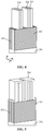
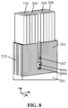
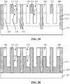
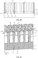
- FIG. 1 - FIG. 28 are schematic structural diagrams showing formation process of the memory structure described in the examples of the present invention.
- the trench-type transistor structure specifically includes a semiconductor substrate, a trench in the semiconductor substrate, a gate in the trench, and a drain area and a source area in the semiconductor substrate located on both sides of the trench.
- the trench-type transistor has its gate connected to word line, its drain area connected to bit line and its source area connected to capacitor. Since some electrons will leak from the source area into the semiconductor substrate when the memory structure is working, storage capacity of DRAM becomes worse. Therefore, how to reduce leakage current of a memory structure has become an urgent problem to be solved.
- the formation method of the memory structure may include: etching the active area, forming two second grooves along the row direction in each active area with the two second grooves formed dividing each active area into a drain located in the middle and two sources located at both sides of the drain or into a source located in the middle and two drains located at both sides of the source and with the two second grooves located at both sides of the second anti-etching dielectric layer, and then removing part of the insulating layer between the first anti-etching dielectric layer and second anti-etching dielectric layer by etching to form a third groove which exposes at least part of the surface of the sidewalls on both sides of the active area at the bottom of the second grooves and part of the surface of the sidewalls of the source and drain on both sides of the second grooves with the third groove in connection with the corresponding second groove; and then forming a gate structure in the second groove and the third groove.
- the gate structure formed in the third groove and the second groove at least covers three side surfaces of the active area (channel area) between source and drain, which increases the area of the gate structure, improves the control of the gate structure over the channel area and limits the leakage path of the leakage current between a plate of the capacitor (the capacitor is used to store data and one of its plates is electrically connected to the source) and the semiconductor substrate, thereby effectively reducing the leakage current, increasing the area of word line (there is word line in the gate structure) and lowering the resistance value of word line.
- FIG. 1 - FIG. 28 are schematic structural diagrams showing formation process of the memory structure described in the examples of the present invention.
- FIG. 10 is a cross-sectional schematic view taken along the cutting line EF in FIG. 9 .
- FIG. 11 is a cross-sectional schematic view taken along the cutting line GH in FIG. 9 .
- FIG. 12 is a cross-sectional schematic view taken along the cutting line LM in FIG. 9 .
- a semiconductor substrate 201 is provided, on which a number of discrete active areas 212 arranged in rows and columns are formed. There are a number of first trenches arranged in a column direction and a number of second trenches arranged in a row direction between adjacent active area. The first trenches are filled with an insulating layer 203 and the second trenches are filled with a first anti-etching dielectric layer 211.
- a number of discrete active areas 212 may be formed by etching the semiconductor substrate 201 or by using an epitaxial process.
- the discrete active areas 212 are formed by etching the semiconductor substrate 201.
- the formation process of the active areas 212 will described in detail below with reference to the accompanying drawings ( FIG. 1 to FIG. 12 ).
- the formation process of the active areas 212 includes the follows.
- FIG. 2 is a cross-sectional schematic view taken along the cutting line AB in FIG. 1.
- FIG. 3 is a cross-sectional schematic view taken along the cutting line CD in FIG. 1 .
- a semiconductor substrate 201 is provided, on which a number of discrete elongated active zones 202 arranged in a column direction are formed.
- a first trench is provided between adjacent elongated active zones 202 and the first trench is filled with an insulating layer 203.
- the semiconductor substrate 201 may be made of silicon (Si), germanium (Ge), silicon germanium (GeSi) or silicon carbide (SiC), or silicon-on-insulator (SOI) or germanium-on-insulator (GOI), or other materials such as gallium arsenide and other group III-V compounds.
- the semiconductor substrate 201 is a silicon substrate.
- the semiconductor substrate is doped with certain impurity ions as required.
- the impurity ions may be N-type impurity ions or P-type impurity ions.
- the doping includes doping in well areas and doping in source and drain areas.
- the elongated active zones 202 are subsequently used to form a number of discrete active areas 212 (refer to FIG. 9 to FIG. 12 ).
- the insulating layer 203 is subsequently used for electrical isolation between the active areas 212.
- the formation process of the elongated active zones 202 and the insulating layer 203 includes the following operations.
- a mask layer is formed on the semiconductor substrate 201 (not shown in accompanying drawings), which mask layer has a number of openings arranged in parallel along the column direction.
- the semiconductor substrate 201 is etched along the openings by using the mask layer as a mask, to form a number of discrete elongated active zones 202 arranged along the column direction in the semiconductor substrate 201 with a first trench between adjacent elongated active zones 202.
- An isolation material layer is formed in the first trench and on the surface of the mask layer, with the isolation material layer filling the first trench.
- the isolation material layer and mask layer on the surface of the elongated active zones 202 are removed by planarizing, to form an insulating layer 203 in the first trench.
- the column direction described in the present application refers to the direction parallel to the x-axis.
- the elongated active zones 202 and the semiconductor substrate 201 are distinguished by dotted lines in FIG. 2 and FIG. 3 .
- the insulating layer 203 may be made of silicon oxide, silicon nitride, silicon oxynitride or other suitable isolation materials.
- the insulating layer 203 is made of silicon nitride.
- first mask patterns 210 arranged along the row direction are formed on the elongated active zones 202 and the insulating layer 203.
- a second mask pattern 204 is formed on the sidewalls on both sides of the first mask patterns 210.
- a number of first mask patterns 210 are arranged in parallel along the row direction with the row direction perpendicular to the column direction.
- the row direction is parallel to the y-axis.
- the position where a fourth groove is subsequently formed in the insulating layer corresponds to the position where the first mask patterns 210 are.
- the position where two second grooves along the row direction are subsequently formed corresponds to the position where the second mask pattern 204 is.
- the first mask patterns 210 and the second mask pattern 204 are made of different materials.
- the first mask patterns 210 are made of silicon nitride
- the second mask pattern 204 is made of silicon oxynitride.
- the first mask patterns 210 and the second mask pattern 204 can be also made of other suitable materials.
- the formation process of the second mask pattern 204 includes the following operations.
- a second mask material layer (not shown in accompanying drawings) is formed on the surface of the first mask patterns 210 and the surface of the elongated active zones 202 and the insulating layer 203.
- the second mask material layer is etched without a mask, to form a second mask pattern 204 on the sidewalls on both sides of the first mask patterns 210.
- no first mask pattern may be formed first, but a second mask pattern may be formed first on the elongated active areas and on the insulating layer. After the second mask pattern is formed, a first mask pattern and a third mask pattern may be subsequently formed simultaneously.
- a third mask pattern 206 is formed on the surface of the sidewall of the second mask pattern 204.
- the formation process of the third mask pattern 206 includes the following operations.
- a third mask material layer 205 is formed on the surface of the first mask patterns 210 and the second mask pattern 204 and on the surface of the elongated active zones 202 and the insulating layer 203.
- the third mask material layer 205 is etched without a mask, to form a third mask pattern 206 on the surface of the sidewall of the second mask pattern 204.
- the third mask pattern 206 is used as a mask in subsequent etching of the elongated active areas and the insulating layer to form a number of second trenches arranged in the row direction in the elongated active areas and the insulating layer.
- the third mask pattern 206 may be made of amorphous carbon or any other suitable material.
- the second mask pattern 204 and the third mask pattern 206 are sequentially formed on the sidewalls on both sides of the first mask patterns 210 in a self-aligned way, which results in higher accuracy in position and size of the first mask patterns 210, the second mask pattern 204 and the third mask pattern 206 and improves the accuracy in position and size of the second trenches, the second groove and the fourth groove subsequently formed, thereby helping to improve the performance of memory structure and simplifying processes by eliminating the process of multiple photoetchings and etchings for forming masks.
- the elongated active zones 201 (refer to FIG. 6 ) and the insulating layer 203 are etched to form a number of second trenches 207 arranged in the row direction in the elongated active zones 201 and the insulating layer 203.
- the elongated active zones 201 are disconnected by the second trenches 207 to form a number of discrete active areas 212 arranged in rows and columns.
- the first trench and the second trenches 207 constitute a first groove.
- the third mask pattern 206, the second mask pattern 204 and the first mask patterns 210 are used as masks when etching the elongated active zones 201 and the insulating layer 203.
- An anisotropic dry etching method may be adopted as the etching process, such as an anisotropic plasma etching process.
- the elongated active zones 202 and the insulating layer 203 at the bottom of the second trenches 207 are further etched after the second trenches 207 are formed, to form a third trench 209a in the elongated active zone and the insulating layer 203 at the bottom of the second trenches 207, with the size of the third trench 209a in the row direction being greater than the size of the second trenches 207 in the row direction.
- a second insulating layer (not shown in accompanying drawings) is formed on the sidewall of the third trench 209a.
- the elongated active zones 202 and the insulating layer 203 at the bottom of the third trench 209a are etched, to form a fourth trench 209b in the elongated active zones 202 and the insulating layer 203 at the bottom of the third trench 209a after the second insulating layer is formed.
- An isotropic etching process is used in etching and forming the third trench 209a.
- the isotropic etching process used is wet etching.
- An anisotropic dry etching process may be used in etching and forming the fourth trench 209b, with the size of the fourth trench 209b being smaller than that of the third trench 209a.
- the size of the third trench 209a in the row direction being greater than the size of the second trenches 207 in the row direction means that the size of the third trench 209a along the y-axis direction is greater than the size of the second trenches 207 along the y-axis direction.
- the bottom size of the first anti-etching dielectric layer formed is relatively large, to reduce the area of the connection portion between the subsequently formed source and the bottom semiconductor substrate, thereby reducing the area of leakage path through which the current in the source flows to the semiconductor substrate and reducing the leakage current.
- a second insulating layer is formed on the sidewall of the third trench 209a
- the size of the third trench 209a and the second trenches 207 refers to the maximum size of the third trench 209a and the second trenches 207 in the y-axis direction.
- the first trench, second trench, third trench and fourth trench described in this example constitute the first groove.
- first trench and the second trench constitute the first groove
- the third trench and the fourth trench may not be formed
- a first anti-etching dielectric layer may be directly formed in the second trench subsequently.
- the depth of the second trenches 207 or the total depth of the second trenches 207 and the third trench 209a is greater than the total depth of the second groove and the third groove formed subsequently.
- the first anti-etching dielectric layer can well isolate adjacent active areas and word lines (gate structure).
- a first anti-etching dielectric layer 211 is formed in the fourth trench 209b, the third trench 209a and the second trenches 207.
- the first anti-etching dielectric layer 211 and the insulating layer 203 are used to isolate adjacent active areas 212.
- a number of active areas 212 are arranged in rows and columns on the semiconductor substrate (refer to FIG. 10 ).
- the first anti-etching dielectric layer 211 formed may be flush with the top surface of the first mask patterns 210.
- the first anti-etching dielectric layer 211 may be made of silicon nitride.
- the first mask patterns 210 are removed (refer to FIG. 12 ) and a number of openings (first openings) 213 along the row direction are formed, with each opening exposing at least part of the surface of the insulating layer 203 on both sides of the active areas 212.
- the first mask patterns 210 may be removed by wet etching. Since the first mask patterns 210 are made of the material different from that of the second mask pattern 204, the third mask pattern 206 and the first anti-etching dielectric layer 211, the etching process may be selected flexibly. Therefore, when the first mask patterns 210 is being removed, the etching rate of the first mask patterns 210 is greater than that of the second mask pattern 204, the third mask pattern 206 and the first anti-etching dielectric layer 211, as a result of which the second mask pattern 204, the third mask pattern 206 and the first anti-etching dielectric layer 211 are less etched or the amount of etching is basically negligible. The second mask pattern 204, the third mask pattern 206 and the first anti-etching dielectric layer 211 are remained as masks for etching the insulating layer 203, to form a fourth groove in the insulating layer 203.
- the insulating layer 203 is etched along the openings 213 by using the mask layers (the second mask pattern 204, the third mask pattern 206 and the first anti-etching dielectric layer 211) as masks, such that the fourth groove 214 is formed in the insulating layer 203, with the fourth groove 214 formed exposing part of the sidewall of active areas.
- the depth of the fourth groove 214 is greater than that of the first anti-etching dielectric layer 211.
- a second anti-etching dielectric layer 215 filling the fourth groove is formed.
- the second anti-etching dielectric layer 215 formed is on the sidewalls of the active areas 212 between the two second grooves formed subsequently and in the insulating layer 203 (refer to FIG. 16 ).
- the second anti-etching dielectric layer 215 is made of the material different from that of the insulating layer, and is made of silicon nitride, silicon oxynitride or any other suitable material.
- the second anti-etching dielectric layer 215 in this example is made of silicon nitride.
- the second anti-etching dielectric layer 215 prevents connection between adjacent second grooves or adjacent third grooves so as to form two independent word lines (gate structure) later when part of the insulating layer between the first anti-etching dielectric layer and the second anti-etching dielectric layer on both sides of the bottom of the second groove is subsequently removed by etching to form a third groove exposing at least part of the surface of the sidewalls on both sides of the active area at the bottom of the second grooves and part of the surface of the sidewalls of the source and drain on both sides of the second grooves.
- the depth of the second anti-etching dielectric layer 215 is greater than the total depth of the third groove and the second groove formed subsequently.
- the width of the second anti-etching dielectric layer 215 in the column direction is greater than the width of the third groove in the column direction, so as to better prevent connection between adjacent second grooves or adjacent third grooves and reduce the difficulties in the process of forming the third groove when the third groove is subsequently formed.
- the formation process of the second anti-etching dielectric layer 215 includes the following operations.
- An anti-etching dielectric material layer is formed in the openings and the fourth groove and on the surface of the second mask pattern 204, the third mask pattern 206 and the first anti-etching dielectric layer 211, with the anti-etching dielectric material layer filling the openings and the fourth groove.
- the anti-etching dielectric material layer on the top surface of the second mask pattern 204, the third mask pattern 206 and the first anti-etching dielectric layer 21 is removed by planarizing, to form a second anti-etching dielectric layer 215 in the openings and the fourth groove.
- the second mask pattern 204 (refer to FIG. 15 ) is removed, to form a number of openings (second openings) 216 arranged along the row direction, with each opening 216 exposing at least the surface of the active areas 212.
- each active area 212 There are two openings 216 on each active area 212.
- two second grooves along the row direction can be formed in each active area 212, with the two second grooves formed dividing each active area 212 into a drain located in the middle and two sources located at both sides of the drain.
- the wet etching process may be used to remove the second mask pattern 204.
- each opening 216 exposes the surface of the insulating layer 203 at the bottom and the sidewall surface of the second anti-etching dielectric layer 215.
- the active areas 212 are etched along the openings 216, and two second grooves 217 distributed along the row direction are formed in each active area 212, with the two second grooves 217 dividing each active area 212 into a drain 218 located in the middle and two sources 220 and 219 located at both sides of the drain 218, and with the two second grooves 217 being located at both sides of the second anti-etching dielectric layer 215 respectively.
- the active areas 212 are etched using the plasma etching process which uses one or more of HBr and Cl 2 as the process gas.
- the two second grooves 217 formed are discrete, and divide each active area 212 into a drain 218 located in the middle and two sources 220 and 219 located at both sides of the drain 218, enabling to subsequently form two common-drain trench-type transistors after word lines (gate structure) are formed.
- the two second grooves 217 formed divide each active area 212 into a source located in the middle and two drains located at both sides of the source, enabling to subsequently form two common-source trench-type transistors after word lines (gate structure) are formed.
- the depth of the second grooves 217 is smaller than that of the first anti-etching dielectric layer 211.
- part of the insulating layer 203 (refer to FIG. 20 ) at the bottom of the openings 216 can be etched and removed at the same time, so that the second grooves 217 formed can extend into the insulating layer 203 on both sides of the active areas 212.
- the depth of the second grooves 217 formed in the insulating layer 203 is equal to or less than that of the second grooves 217 formed in the active areas 212.
- the material of the active areas 212 has a higher etching selectivity than that of the insulating layer 203.
- the insulating layer at the bottom of the openings 216 will not be etched or will be little etched, so that the second grooves 217 formed are only in the active areas 212.
- the two second grooves 217 formed divide each active area 212 into a source located in the middle and two drains located at both sides of the source, with one of the two drains subsequently being connected to the capacitor of memory structure and the source being connected to the bit line.
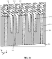
- FIG. 21 is a three-dimensional schematic diagram showing the process of etching the active areas 212 along the openings 216 and forming two second grooves 217 along the row direction in each active area 212 with the two second grooves 217 dividing each active area 212 into a drain 218 located in the middle and two sources 220 and 219 located at both sides of the drain 218.
- the part of the first anti-etching dielectric layer 211 (refer to FIG. 19 to FIG. 20 ), the second anti-etching dielectric layer 215 (refer to FIG. 19 to FIG. 20 ) and the third mask pattern 206 (refer to FIG. 19 to FIG. 20 ) above the top surface of the active areas (the sources 220/219 and the drain 218) is not shown.
- FIG. 23 is a cross-sectional schematic view taken in the direction of the cutting line A3B3 in FIG. 22 and FIG. 24 is a cross-sectional schematic view taken in the direction of the cutting line A4B4 in FIG.
- part of the insulating layer 203 between the first anti-etching dielectric layer 211 and the second anti-etching dielectric layer 215 is etched and removed, and a third groove 221 is formed which exposes at least part of the surface of the sidewalls on both sides of the active areas 212 (two sidewalls in the x-axis direction) at the bottom of the second grooves 217 and part of the surface of the sidewalls (two sidewalls in the x-axis direction) of the sources 219/220 and the drain 218 at both sides of the second grooves 217, with the third groove 221 in connection with the corresponding second grooves 217.
- Part of the insulating layer 203 between the first anti-etching dielectric layer 211 and the second anti-etching dielectric layer 215 is etched and removed. During etching, the first anti-etching dielectric layer 211 and the second anti-etching dielectric layer 215 can prevent two adjacent second grooves 217 and two adjacent third grooves 221 from connection.
- the third groove 221 not only exposes part of the surface of the sidewalls on both sides of the active areas 212 at the bottom of the second grooves 217 and part of the surface of the sidewalls of the sources 219/220 and the drain 218 on both sides of the second grooves 217, but also exposes part of the sidewall surface of the second trench or the third trench or part of the surface of one sidewall of the active areas 212 away from the second grooves 217.
- each active area has four sidewalls, including two opposite sidewalls in the x-axis direction (row direction) and two opposite sidewalls in the y-axis direction (column direction).
- the third grooves 221 include a first portion 221a and a second portion 221b that are connected to each other.
- the first portion 221a is located on the insulating layer 203 on both sides of the bottom of the second grooves 217 and between the first anti-etching dielectric layer 211 and the second anti-etching dielectric layer 215.
- the first portion 221a exposes part of the surface of the sidewalls (two opposite sidewalls in the y-axis direction (column direction)) on both sides of the active areas 212 at the bottom of the second grooves 217 and part of the surface of the sidewalls (two sidewalls in the x-axis direction (column direction)) of the sources 219/220 and the drain 218 on both sides of the second grooves 217.
- the second portion 221b is located between the active areas 212 and the first anti-etching dielectric layer 211.
- the second portion 221b exposes part of the surface of one sidewall (a sidewall in the y-axis direction (row direction)) of the active areas 212 away from the second grooves 217 and part of the surface of the first anti-etching dielectric layer 211.
- the second portion 221b is in connection with the first portion 221a.
- the structure of the third grooves 221 enables the gate structure formed to surround the peripheral sidewalls of the active areas 212 (channel areas) between the source 220 and the drain 218, which enlarges the area of the gate structure, improves the control of the gate structure on the channel areas and further limits leakage path of the leakage current between a plate of the capacitor (the capacitor is used to store data and one of its plates is electrically connected to the source) and the semiconductor substrate, thereby effectively reducing the leakage current, increasing the area of word line (the gate structure includes word line) and lowering the resistance value of word line.
- the third grooves only expose part of the surface of the sidewalls on both sides of the active areas at the bottom of the second grooves and part of the surface of the sidewalls of the source and the drain on both sides of the second grooves.
- a third groove structure enables the gate structure to at least cover three sides of the active areas 212 (channel areas) between the source 220 and the drain 218, which increases the area of the gate structure, improves the control of the gate structure over the channel area and limits the leakage path of the leakage current between a plate of the capacitor (the capacitor is used to store data and one of its plates electrically connected to the source) and the semiconductor substrate, thereby effectively reducing the leakage current, increasing the area of word line (the gate structure includes word line) and lowering the resistance value of word line.
- FIG. 26 is a three-dimensional schematic diagram of the gate structure
- FIG. 27 is a cross-sectional schematic view of FIG. 25 taken along the cutting line A1B1
- FIG. 28 is a cross-sectional schematic view of FIG. 25 taken along the cutting line A2B2
- a gate structure 223 is formed in the second grooves and the third grooves.
- the gate structure 223 includes: a gate dielectric layer on the surface of the sidewalls of the second grooves and the third grooves; and a word line on the gate dielectric layer and filling the second grooves and the third grooves.
- the gate dielectric layer is made of a high-K dielectric material, such as HfO 2 , TiO 2 , HfZrO, HfSiNO, Ta 2 O 5 , ZrO 2 , ZrSiO 2 , Al 2 O 3 , SrTiO 3 or BaSrTiO.
- the word line is made of one or more metal materials of W, Al, Cu, Ti, Ag, Au, Pt and Ni.
- the gate dielectric layer may be made of silicon oxide, and the word line may be made of polysilicon.
- the formation process of the gate structure includes the following operations.
- a gate dielectric material layer is formed on the surface of the sidewall and bottom of the third grooves and the second grooves.
- a word line material layer is formed on the gate dielectric material layer.
- the gate dielectric material layer and the word line material layer on the top surface of the sources 220/219 and the drain 218 are removed to form a gate structure in the third grooves and the second grooves.
- the gate structure includes a gate dielectric layer on the surface of the sidewalls of the second grooves and the third grooves, and a word line located on the gate dielectric layer and filling the second grooves and the third grooves.
- the chemical mechanical polishing process or the etch-back process may be used to remove the gate dielectric material layer and the word line material layer on the top surface of the sources 220/219 and the drain 218.
- the third mask pattern 206 (refer to FIG. 19 ), the second anti-etching dielectric layer 215 and the first anti-etching dielectric layer 211 on the top surface of the sources 220/219 and the drain 218 can be removed at the same time when the gate dielectric material layer and the word line material layer on the top surface of the sources 220/219 and the drain 218 are removed.
- the gate structure 223 formed includes a first portion 223a, a second portion 223b and a third portion 223c that are connected with each other.
- the first portion 223a of the gate structure 223 is filled in the second grooves 217 (refer to FIG. 22 ).
- the second portion 223b of the gate structure 223 is filled in the first portion 221a of the third grooves 221 (refer to FIG. 22 ).
- the third portion 223c of the gate structure 223 is filled in the second portion 221b of the third grooves 221 (refer to FIG. 22 ).
- the formation method of the memory structure further includes the following operations.
- a bit line connected to the gate is formed.
- a capacitor connected to the source 220 (or the source 219) is formed on the insulating layer 203 (not shown in accompanying drawings).
- a bit line connected to the drain 218 is formed on the insulating layer 203 (not shown in accompanying drawings).
- the examples of the present invention also provide a memory structure.
- the memory structure includes a semiconductor substrate 201, a second anti-etching dielectric layer 215, second grooves 217, a third groove, and a gate structure 223.
- a number of discrete active areas 212 arranged in rows and columns are formed on the semiconductor substrate 201.
- the first trenches are filled with an insulating layer 203 and the second trenches are filled with a first anti-etching dielectric layer 211.
- the second anti-etching dielectric layer 215 is located on the sidewall surface of the active area 212 between adjacent first anti-etching dielectric layers 211 and in the insulating layer 203.
- Two second grooves 217 is arranged along the row direction in each active area.
- the two second grooves 217 divide each active area into a drain 218 located in the middle and two sources 219/220 located at both sides of the drain 218.
- the two second grooves 217 are respectively located at both sides of the second anti-etching dielectric layer 215.
- the surface of the insulating layer 203 is lower than the bottom surface of the second grooves 217.
- the third groove is located on the insulating layer 203 between the first anti-etching dielectric layer 211 and the second anti-etching dielectric layer 215.
- the third groove exposes at least part of the surface of the sidewalls on both sides of the active areas 212 at the bottom of the second grooves 217 and part of the surface of the sidewalls of the source and drain at both sides of the second grooves 217.
- the third groove is in connection with the corresponding second groove.
- the gate structure 223 is located in the second groove and the third groove.
- the first anti-etching dielectric layer 211 and the second anti-etching dielectric layer 215 are made of the material different from that of the insulating layer.
- either one of the depth of the first anti-etching dielectric layer 211 and the depth of the second anti-etching dielectric layer 215 is greater than the total depth of the third groove and the second groove.
- the size of the third trench in the row direction is larger than the size of the second trenches in the row direction.
- the first anti-etching dielectric layer is arranged in the fourth trench, the third trench and the second trench.
- the third groove in addition to exposing part of the surface of the sidewalls on both sides of the active area at the bottom of the second groove and part of the sidewall surface of the source and drain on both sides of the second groove, the third groove also exposes part of the sidewall surface of the second trench or the third trench, or part of the surface of one sidewall of the active area away from the second groove.
- the third groove only exposes part of the surface of the sidewalls on both sides of the active area at the bottom of the second groove and part of the sidewall surface of the source and drain on both sides of the second groove.
- the gate structure 223 includes: a gate dielectric layer located on the sidewall surfaces of the second groove and the third groove; and a word line located on the gate dielectric layer and filled with the second groove and the third groove.
- the gate structure 223 formed includes a first portion 223a, a second portion 223b and a third portion 223c that are connected with each other.
- the first portion 223a of the gate structure 223 is filled in the second grooves 217 (refer to FIG. 22 ).
- the second portion 223b of the gate structure 223 is filled in the first portion 221a of the third grooves 221 (refer to FIG. 22 ).
- the third portion 223c is filled in the second portion 221b of the third grooves 221 (refer to FIG. 22 ).
- the memory structure also includes a word line connected to the gate, a capacitor connected to the source 219 (or the source 220) and on the insulating layer 203 (not shown in accompanying drawings), and a bit line connected to the drain 218 and on the insulating layer 203 (not shown in accompanying drawings).
Landscapes
- Engineering & Computer Science (AREA)
- Manufacturing & Machinery (AREA)
- Semiconductor Memories (AREA)
Abstract
Description
- The present invention relates to the field of memory, in particular to a memory structure and a method for forming the same.
- Dynamic Random Access Memory (DRAM) is a semiconductor memory device commonly used in computers and is composed of many repeated memory cells. Each memory cell usually includes a capacitor and a transistor. The transistor has its gate connected to word line, its drain connected to bit line and its source connected to capacitor. Voltage signal on the word line can control on or off of the transistor and then the data information stored in the capacitor can be read through the bit line or the data information can be written into the capacitor through the bit line for storage.
- However, since the memory structure composed of capacitor and transistor in existing memories is prone to leakage current, the performance of existing memories need to be further improved.
- The technical problem of the present invention is to reduce the leakage current of the memory structure composed of capacitor and transistor in memories.
- To this end, the present invention provides a method for forming a memory structure, which includes the following operations.
- A semiconductor substrate is provided, on which a number of discrete active areas arranged in rows and columns are formed. A first groove is formed between adjacent active areas. The first groove includes a number of first trenches arranged in a column direction and a number of second trenches arranged in a row direction. The first trenches are filled with an insulating layer and the second trenches are filled with a first anti-etching dielectric layer.
- A second anti-etching dielectric layer is formed on the sidewall surface of the active areas between adjacent first anti-etching dielectric layers and in the insulating layer.
- Each of the active areas is etched to form two second grooves along the row direction in each of the active areas. The two second grooves divide each active area into a drain located in the middle and two sources located at both sides of the drain. The two second grooves are respectively located on both sides of the second anti-etching dielectric layer.
- Part of the insulating layer between the first anti-etching dielectric layer and the second anti-etching dielectric layer are removed by etching, to form a third groove which exposes at least part of the surface of the sidewalls on both sides of the active area at the bottom of the second grooves and part of the surface of the sidewalls of the source and drain on both sides of the second grooves. The third groove is in connection with the corresponding second groove.
- A gate structure is formed in the second groove and the third groove.
- Optionally, the first anti-etching dielectric layer and the second anti-etching dielectric layer are made of a material different from that of the insulating layer.
- Optionally, either one of a depth of the first anti-etching dielectric layer and a depth of the second anti-etching dielectric layer is greater than a total depth of the third groove and the second groove.
- Optionally, the formation process of the second anti-etching dielectric layer includes the following operations. A mask layer is formed on the insulating layer and the active areas, which mask layer has a number of openings along the row direction with each opening exposing at least part of the surface of the insulating layer on both sides of each of the active areas. The insulating layer is etched along the openings by using the mask layer as a mask to form a fourth groove in the insulating layer, with the fourth groove exposing part of the sidewall of the active areas. A second anti-etching dielectric layer filling the fourth groove is formed.
- Optionally, the specific process of forming a number of discrete active areas arranged in rows and columns on the semiconductor substrate includes the following operations. A number of discrete elongated active zones arranged in a column direction are formed on the semiconductor substrate, with a second trench between adjacent elongated active zones and with the first trench filled with an insulating layer. The elongated active zones and the insulating layer are etched, to form a number of second trenches arranged in a row direction in the elongated active zones and the insulating layer, with the second trenches formed disconnecting the elongated active zones to form a number of discrete active areas arranged in rows and columns. A first anti-etching dielectric layer filling the second trenches is formed.
- Optionally, the elongated active zones and the insulating layer at the bottom of the second trenches are etched to form a third trench in the elongated active zones and the insulating layer at the bottom of the second trenches before forming the first anti-etching dielectric layer, with the size of the third trench in the row direction being larger than the size of the second trenches in the row direction. A second insulating layer is formed on the sidewall of the third trench. The elongated active zones and the insulating layer at the bottom of the third trench are etched, to form a fourth trench in the elongated active zones and the insulating layer at the bottom of the third trench, after the second insulating layer is formed. A first anti-etching dielectric layer is formed in the fourth trench, the third trench and the second trench.
- Optionally, the depth of the second trench or the total depth of the second trench, the third trench and the fourth trench is greater than the total depth of the second groove and the third groove.
- Optionally, the second insulating layer is removed while part of the insulating layer between the first anti-etching dielectric layer and the second anti-etching dielectric layer is removed by etching.
- Optionally, in addition to exposing part of the surface of the sidewalls on both sides of the active area at the bottom of the second groove and part of the sidewall surface of the source and drain on both sides of the second groove, the third groove also exposes part of the sidewall surface of the second trench or the third trench, or part of the surface of one sidewall of the active area away from the second groove.
- Optionally, the third groove only exposes part of the surface of the sidewalls on both sides of the active area at the bottom of the second groove and part of the sidewall surface of the source and drain on both sides of the second groove.
- Optionally, the gate structure includes a gate dielectric layer located on the sidewall surfaces of the second groove and the third groove, and a word line located on the gate dielectric layer and filled in the second groove and the third groove.
- Optionally, the method proposed in the present invention also includes: forming a bit line connected to the gate; forming a capacitor connected to the source and on the insulating layer; and forming a bit line connected to the drain and on the insulating layer.
- The present invention further provides a memory structure, which comprises:
- a semiconductor substrate on which a number of discrete active areas arranged in rows and columns are formed. A first groove is formed between adjacent active areas. The first groove includes a number of first trenches arranged in a column direction and a number of second trenches arranged in a row direction. The first trenches are filled with an insulating layer and the second trenches are filled with a first anti-etching dielectric layer;
- a second anti-etching dielectric layer on the sidewall surface of the active areas between adjacent first anti-etching dielectric layers and in the insulating layer;
- two second grooves along the row direction in each of the active areas. The two second grooves divide each active area into a drain located in the middle and two sources located at both sides of the drain. The two second grooves are respectively located at both sides of the second anti-etching dielectric layer. The surface of the insulating layer is lower than the bottom surface of the second groove;
- a third groove on the insulating layer between the first anti-etching dielectric layer and the second anti-etching dielectric layer, which exposes at least part of the surface of the sidewalls on both sides of the active area at the bottom of the second grooves and part of the surface of the sidewalls of the source and drain on both sides of the second grooves. The third groove is in connection with the corresponding second groove; and
- a gate structure in the second groove and the third groove.
- Optionally, the first anti-etching dielectric layer and the second anti-etching dielectric layer are made of a material different from that of the insulating layer.
- Optionally, either one of the depth of the first anti-etching dielectric layer and the depth the second anti-etching dielectric layer is greater than the total depth of the third groove and the second groove.
- Optionally, there is a third trench in the elongated active zone and the insulating layer at the bottom of the second trench, with the size of the third trench in the row direction being greater than the size of the second trench in the row direction. There is a fourth trench in the elongated active zone and the insulating layer at the bottom of the third trench. The first anti-etching dielectric layer is located in the fourth trench, the third trench and the second trench.
- Optionally, in addition to exposing part of the surface of the sidewalls on both sides of the active area at the bottom of the second groove and part of the sidewall surface of the source and drain on both sides of the second groove, the third groove also exposes part of the sidewall surface of the second trench or the third trench, or part of the surface of one sidewall of the active area away from the second groove.
- Optionally, the third groove only exposes part of the surface of the sidewalls on both sides of the active area at the bottom of the second groove and part of the sidewall surface of the source and drain on both sides of the second groove.
- Optionally, the gate structure includes: a gate dielectric layer located on the sidewall surfaces of the second groove and the third groove; and a gate located on the gate dielectric layer and filled in the second groove and the third groove.
- Optionally, the memory structure also includes: a bit line connected to the gate; a capacitor connected to the source and on the insulating layer; and a bit line connected to the drain and on the insulating layer.
- Compared with the prior art, the technical solutions proposed in the present invention have the following advantages.
- The method for forming the memory structure of the present invention includes: etching the active area, forming two second grooves along the row direction in each active area with the two second grooves formed dividing each active area into a drain located in the middle and two sources located at both sides of the drain or into a source located in the middle and two drains located at both sides of the source and with the two second grooves located at both sides of the second anti-etching dielectric layer, and then removing part of the insulating layer between the first anti-etching dielectric layer and second anti-etching dielectric layer by etching to form a third groove which exposes at least part of the surface of the sidewalls on both sides of the active area at the bottom of the second grooves and part of the surface of the sidewalls of the source and drain on both sides of the second grooves with the third groove in connection with the corresponding second groove; and then forming a gate structure in the second groove and the third groove. By forming the aforementioned third groove structure, the gate structure formed in the third groove and the second groove at least covers three sides of the active area (channel area) between source and drain, which increases the area of the gate structure, improves the control of the gate structure over the channel area and limits the leakage path of the leakage current between a plate of the capacitor (the capacitor is used to store data and one of its plates is electrically connected to the source) and the semiconductor substrate, thereby effectively reducing the leakage current, increasing the area of word line (the gate structure includes word line) and lowering the resistance value of word line.
- Furthermore, in addition to exposing part of the surface of the sidewalls on both sides of the active area at the bottom of the second grooves and part of the surface of the sidewalls of the source and drain on both sides of the second grooves, the third groove also exposes part of the sidewall surface of the second trench or the third trench or part of the surface of one sidewall of the active area away from the second groove. After a gate structure is formed in the third groove and the second groove, such the third groove structure makes the gate structure surround the peripheral sidewalls of the active area (channel area) between source and drain and therefore increases the area of the gate structure, improves the control of the gate structure over the channel area and further limits the leakage path of the leakage current between a plate of the capacitor (the capacitor is used to store data and one of its plates is electrically connected to the source) and the semiconductor substrate, thereby effectively reducing the leakage current, increasing the area of word line (the gate structure includes word line) and lowering the resistance value of word line.
- Furthermore, the size of the third trench in the row direction is greater than the size of the second trench in the row direction. On the one hand, when the first anti-etching dielectric layer is subsequently formed, the bottom size of the first anti-etching dielectric layer formed is relatively large to reduce the area of the connection portion between the subsequently formed source and the bottom semiconductor substrate, thereby reducing the area of leakage path through which the current in the source flows to the semiconductor substrate and reducing the leakage current. On the other hand, after a second insulating layer is formed on the sidewall of the third trench, it is convenient for subsequently removing the second insulating layer while part of the insulating layer between the first anti-etching dielectric layer and the second anti-etching dielectric layer is removed by etching to form a third groove, so as to easily ensure that the third groove formed not only exposes part of the surface of the sidewalls on both sides of the active area at the bottom of the second groove and part of the sidewall surface of the source and drain on both sides of the second groove, but also exposes part of the sidewall surface of the second trench or the third trench or part of the surface of one sidewall of the active area away from the second groove.
- The memory structure proposed in the present invention includes two second grooves along the row direction in each active area. The two second grooves divide each active area into a drain located in the middle and two sources located at both sides of the drain or into a source located in the middle and two drains located at both sides of the source. The two second grooves are located at both sides of the second anti-etching dielectric layer respectively. The surface of the insulating layer is lower than the bottom surface of the second groove. The memory structure includes a third groove on the insulating layer between the first anti-etching dielectric layer and the second anti-etching dielectric layer. The third groove exposes at least part of the surface of the sidewalls on both sides of the active area at the bottom of the second grooves and part of the surface of the sidewalls of the source and drain on both sides of the second grooves. The third groove is in connection with the corresponding second groove. The memory structure includes a gate structure in the second groove and the third groove. Such configuration enables the gate structure to at least cover three sides of the active area (channel area) between source and drain, which increases the area of the gate structure, improves the control of the gate structure over the channel area and limits the leakage path of the leakage current between a plate of the capacitor (the capacitor is used to store data and one of its plates is electrically connected to the source) and the semiconductor substrate, thereby effectively reducing the leakage current, increasing the area of word line (the gate structure includes word line) and lowering the resistance value of word line.
-
FIG. 1 - FIG. 28 are schematic structural diagrams showing formation process of the memory structure described in the examples of the present invention. - As described in the "BACKGROUND" section above, existing memory structures are prone to leakage current, and the performance of existing memories need to be improved.
- Studies have found that in order to improve the integration of memory structures, the trench-type transistor structure is currently used. The trench-type transistor structure specifically includes a semiconductor substrate, a trench in the semiconductor substrate, a gate in the trench, and a drain area and a source area in the semiconductor substrate located on both sides of the trench. The trench-type transistor has its gate connected to word line, its drain area connected to bit line and its source area connected to capacitor. Since some electrons will leak from the source area into the semiconductor substrate when the memory structure is working, storage capacity of DRAM becomes worse. Therefore, how to reduce leakage current of a memory structure has become an urgent problem to be solved.
- To this end, the disclosure provides a memory structure and its formation method. The formation method of the memory structure may include: etching the active area, forming two second grooves along the row direction in each active area with the two second grooves formed dividing each active area into a drain located in the middle and two sources located at both sides of the drain or into a source located in the middle and two drains located at both sides of the source and with the two second grooves located at both sides of the second anti-etching dielectric layer, and then removing part of the insulating layer between the first anti-etching dielectric layer and second anti-etching dielectric layer by etching to form a third groove which exposes at least part of the surface of the sidewalls on both sides of the active area at the bottom of the second grooves and part of the surface of the sidewalls of the source and drain on both sides of the second grooves with the third groove in connection with the corresponding second groove; and then forming a gate structure in the second groove and the third groove. By forming the aforementioned third groove structure, the gate structure formed in the third groove and the second groove at least covers three side surfaces of the active area (channel area) between source and drain, which increases the area of the gate structure, improves the control of the gate structure over the channel area and limits the leakage path of the leakage current between a plate of the capacitor (the capacitor is used to store data and one of its plates is electrically connected to the source) and the semiconductor substrate, thereby effectively reducing the leakage current, increasing the area of word line (there is word line in the gate structure) and lowering the resistance value of word line.
- In order to give a clearer explanation on the aforesaid purposes, characteristics and advantages of the present invention, the specific examples of the present invention are described in detail below with reference to the accompanying drawings. When describing the examples of the present invention in detail, the schematic diagrams attached hereto, for illustrative purposes, are not partially enlarged based on the regular scale, and should not limit the protection scope of the present invention but only serve as examples. Besides, the three-dimensional size of length, width and depth should be included in practical application.
-
FIG. 1 - FIG. 28 are schematic structural diagrams showing formation process of the memory structure described in the examples of the present invention. - As shown in
FIG. 9 to FIG. 12 ,FIG. 10 is a cross-sectional schematic view taken along the cutting line EF inFIG. 9 .FIG. 11 is a cross-sectional schematic view taken along the cutting line GH inFIG. 9 .FIG. 12 is a cross-sectional schematic view taken along the cutting line LM inFIG. 9 . Asemiconductor substrate 201 is provided, on which a number of discreteactive areas 212 arranged in rows and columns are formed. There are a number of first trenches arranged in a column direction and a number of second trenches arranged in a row direction between adjacent active area. The first trenches are filled with an insulatinglayer 203 and the second trenches are filled with a first anti-etchingdielectric layer 211. - A number of discrete
active areas 212 may be formed by etching thesemiconductor substrate 201 or by using an epitaxial process. - In this example, the discrete
active areas 212 are formed by etching thesemiconductor substrate 201. The formation process of theactive areas 212 will described in detail below with reference to the accompanying drawings (FIG. 1 to FIG. 12 ). The formation process of theactive areas 212 includes the follows. - As shown in
FIG. 1 to FIG. 3, FIG. 2 is a cross-sectional schematic view taken along the cutting line AB inFIG. 1. FIG. 3 is a cross-sectional schematic view taken along the cutting line CD inFIG. 1 . Asemiconductor substrate 201 is provided, on which a number of discrete elongatedactive zones 202 arranged in a column direction are formed. A first trench is provided between adjacent elongatedactive zones 202 and the first trench is filled with an insulatinglayer 203. - The
semiconductor substrate 201 may be made of silicon (Si), germanium (Ge), silicon germanium (GeSi) or silicon carbide (SiC), or silicon-on-insulator (SOI) or germanium-on-insulator (GOI), or other materials such as gallium arsenide and other group III-V compounds. In this example, thesemiconductor substrate 201 is a silicon substrate. The semiconductor substrate is doped with certain impurity ions as required. The impurity ions may be N-type impurity ions or P-type impurity ions. In an example, the doping includes doping in well areas and doping in source and drain areas. - The elongated
active zones 202 are subsequently used to form a number of discrete active areas 212 (refer toFIG. 9 to FIG. 12 ). The insulatinglayer 203 is subsequently used for electrical isolation between theactive areas 212. In an example, the formation process of the elongatedactive zones 202 and the insulatinglayer 203 includes the following operations. A mask layer is formed on the semiconductor substrate 201 (not shown in accompanying drawings), which mask layer has a number of openings arranged in parallel along the column direction. Thesemiconductor substrate 201 is etched along the openings by using the mask layer as a mask, to form a number of discrete elongatedactive zones 202 arranged along the column direction in thesemiconductor substrate 201 with a first trench between adjacent elongatedactive zones 202. An isolation material layer is formed in the first trench and on the surface of the mask layer, with the isolation material layer filling the first trench. The isolation material layer and mask layer on the surface of the elongatedactive zones 202 are removed by planarizing, to form an insulatinglayer 203 in the first trench. It should be noted that the column direction described in the present application refers to the direction parallel to the x-axis. For illustrative purposes, the elongatedactive zones 202 and thesemiconductor substrate 201 are distinguished by dotted lines inFIG. 2 and FIG. 3 . - The insulating
layer 203 may be made of silicon oxide, silicon nitride, silicon oxynitride or other suitable isolation materials. In this example, the insulatinglayer 203 is made of silicon nitride. - As shown in
FIG. 4 , a number offirst mask patterns 210 arranged along the row direction are formed on the elongatedactive zones 202 and the insulatinglayer 203. Asecond mask pattern 204 is formed on the sidewalls on both sides of thefirst mask patterns 210. - A number of
first mask patterns 210 are arranged in parallel along the row direction with the row direction perpendicular to the column direction. In this example, the row direction is parallel to the y-axis. - The position where a fourth groove is subsequently formed in the insulating layer corresponds to the position where the
first mask patterns 210 are. The position where two second grooves along the row direction are subsequently formed corresponds to the position where thesecond mask pattern 204 is. - In this example, the
first mask patterns 210 and thesecond mask pattern 204 are made of different materials. In one example, thefirst mask patterns 210 are made of silicon nitride, and thesecond mask pattern 204 is made of silicon oxynitride. In other examples, thefirst mask patterns 210 and thesecond mask pattern 204 can be also made of other suitable materials. - In one example, the formation process of the
second mask pattern 204 includes the following operations. A second mask material layer (not shown in accompanying drawings) is formed on the surface of thefirst mask patterns 210 and the surface of the elongatedactive zones 202 and the insulatinglayer 203. The second mask material layer is etched without a mask, to form asecond mask pattern 204 on the sidewalls on both sides of thefirst mask patterns 210. - In other examples, no first mask pattern may be formed first, but a second mask pattern may be formed first on the elongated active areas and on the insulating layer. After the second mask pattern is formed, a first mask pattern and a third mask pattern may be subsequently formed simultaneously.
- As shown in
FIG. 4 and FIG. 5 , athird mask pattern 206 is formed on the surface of the sidewall of thesecond mask pattern 204. - In one example, the formation process of the
third mask pattern 206 includes the following operations. A thirdmask material layer 205 is formed on the surface of thefirst mask patterns 210 and thesecond mask pattern 204 and on the surface of the elongatedactive zones 202 and the insulatinglayer 203. The thirdmask material layer 205 is etched without a mask, to form athird mask pattern 206 on the surface of the sidewall of thesecond mask pattern 204. - The
third mask pattern 206 is used as a mask in subsequent etching of the elongated active areas and the insulating layer to form a number of second trenches arranged in the row direction in the elongated active areas and the insulating layer. Thethird mask pattern 206 may be made of amorphous carbon or any other suitable material. - In this example, with respect to the mask structure of the
first mask patterns 210, thesecond mask pattern 204 and thethird mask pattern 206, thesecond mask pattern 204 and thethird mask pattern 206 are sequentially formed on the sidewalls on both sides of thefirst mask patterns 210 in a self-aligned way, which results in higher accuracy in position and size of thefirst mask patterns 210, thesecond mask pattern 204 and thethird mask pattern 206 and improves the accuracy in position and size of the second trenches, the second groove and the fourth groove subsequently formed, thereby helping to improve the performance of memory structure and simplifying processes by eliminating the process of multiple photoetchings and etchings for forming masks. - As shown in
FIG. 7 , the elongated active zones 201 (refer toFIG. 6 ) and the insulatinglayer 203 are etched to form a number ofsecond trenches 207 arranged in the row direction in the elongatedactive zones 201 and the insulatinglayer 203. The elongatedactive zones 201 are disconnected by thesecond trenches 207 to form a number of discreteactive areas 212 arranged in rows and columns. The first trench and thesecond trenches 207 constitute a first groove. - In this example, the
third mask pattern 206, thesecond mask pattern 204 and thefirst mask patterns 210 are used as masks when etching the elongatedactive zones 201 and the insulatinglayer 203. An anisotropic dry etching method may be adopted as the etching process, such as an anisotropic plasma etching process. - In this example, as shown in
FIG. 8 , the elongatedactive zones 202 and the insulatinglayer 203 at the bottom of thesecond trenches 207 are further etched after thesecond trenches 207 are formed, to form athird trench 209a in the elongated active zone and the insulatinglayer 203 at the bottom of thesecond trenches 207, with the size of thethird trench 209a in the row direction being greater than the size of thesecond trenches 207 in the row direction. A second insulating layer (not shown in accompanying drawings) is formed on the sidewall of thethird trench 209a. The elongatedactive zones 202 and the insulatinglayer 203 at the bottom of thethird trench 209a are etched, to form afourth trench 209b in the elongatedactive zones 202 and the insulatinglayer 203 at the bottom of thethird trench 209a after the second insulating layer is formed. - An isotropic etching process is used in etching and forming the
third trench 209a. In one example, the isotropic etching process used is wet etching. An anisotropic dry etching process may be used in etching and forming thefourth trench 209b, with the size of thefourth trench 209b being smaller than that of thethird trench 209a. - In this example, the size of the
third trench 209a in the row direction being greater than the size of thesecond trenches 207 in the row direction means that the size of thethird trench 209a along the y-axis direction is greater than the size of thesecond trenches 207 along the y-axis direction. On the one hand, when the first anti-etching dielectric layer is subsequently formed, the bottom size of the first anti-etching dielectric layer formed is relatively large, to reduce the area of the connection portion between the subsequently formed source and the bottom semiconductor substrate, thereby reducing the area of leakage path through which the current in the source flows to the semiconductor substrate and reducing the leakage current. On the other hand, after a second insulating layer is formed on the sidewall of thethird trench 209a, it is convenient for subsequently removing the second insulating layer while part of the insulating layer between the first anti-etching dielectric layer and the second anti-etching dielectric layer is removed by etching to form a third groove, so as to easily ensure that the third groove formed not only exposes part of the surface of the sidewalls on both sides of the active area at the bottom of the second groove and part of the sidewall surface of the source and drain on both sides of the second groove, but also exposes part of the sidewall surface of the second trench or the third trench or part of the surface of one sidewall of the active area away from the second groove. It should be noted that the size of thethird trench 209a and thesecond trenches 207 refers to the maximum size of thethird trench 209a and thesecond trenches 207 in the y-axis direction. The first trench, second trench, third trench and fourth trench described in this example constitute the first groove. - It should be noted that in other examples, the first trench and the second trench constitute the first groove, the third trench and the fourth trench may not be formed, and a first anti-etching dielectric layer may be directly formed in the second trench subsequently.
- The depth of the
second trenches 207 or the total depth of thesecond trenches 207 and thethird trench 209a is greater than the total depth of the second groove and the third groove formed subsequently. When a first anti-etching dielectric layer is subsequently formed in thesecond trenches 207 or in thesecond trenches 207 and thethird trench 209a, the first anti-etching dielectric layer can well isolate adjacent active areas and word lines (gate structure). - As shown in
FIG. 9 to FIG. 12 , a first anti-etchingdielectric layer 211 is formed in thefourth trench 209b, thethird trench 209a and thesecond trenches 207. - The first anti-etching
dielectric layer 211 and the insulatinglayer 203 are used to isolate adjacentactive areas 212. A number ofactive areas 212 are arranged in rows and columns on the semiconductor substrate (refer toFIG. 10 ). - In this example, the first anti-etching
dielectric layer 211 formed may be flush with the top surface of thefirst mask patterns 210. The first anti-etchingdielectric layer 211 may be made of silicon nitride. - As shown in
FIG. 13 which is based onFIG. 12 , thefirst mask patterns 210 are removed (refer toFIG. 12 ) and a number of openings (first openings) 213 along the row direction are formed, with each opening exposing at least part of the surface of the insulatinglayer 203 on both sides of theactive areas 212. - The
first mask patterns 210 may be removed by wet etching. Since thefirst mask patterns 210 are made of the material different from that of thesecond mask pattern 204, thethird mask pattern 206 and the first anti-etchingdielectric layer 211, the etching process may be selected flexibly. Therefore, when thefirst mask patterns 210 is being removed, the etching rate of thefirst mask patterns 210 is greater than that of thesecond mask pattern 204, thethird mask pattern 206 and the first anti-etchingdielectric layer 211, as a result of which thesecond mask pattern 204, thethird mask pattern 206 and the first anti-etchingdielectric layer 211 are less etched or the amount of etching is basically negligible. Thesecond mask pattern 204, thethird mask pattern 206 and the first anti-etchingdielectric layer 211 are remained as masks for etching the insulatinglayer 203, to form a fourth groove in the insulatinglayer 203. - As shown in
FIG. 14 , the insulatinglayer 203 is etched along theopenings 213 by using the mask layers (thesecond mask pattern 204, thethird mask pattern 206 and the first anti-etching dielectric layer 211) as masks, such that the fourth groove 214 is formed in the insulatinglayer 203, with the fourth groove 214 formed exposing part of the sidewall of active areas. - The depth of the fourth groove 214 is greater than that of the first anti-etching
dielectric layer 211. - As shown in
FIG. 15 , a second anti-etchingdielectric layer 215 filling the fourth groove is formed. - The second anti-etching
dielectric layer 215 formed is on the sidewalls of theactive areas 212 between the two second grooves formed subsequently and in the insulating layer 203 (refer toFIG. 16 ). The second anti-etchingdielectric layer 215 is made of the material different from that of the insulating layer, and is made of silicon nitride, silicon oxynitride or any other suitable material. The second anti-etchingdielectric layer 215 in this example is made of silicon nitride. The second anti-etchingdielectric layer 215 prevents connection between adjacent second grooves or adjacent third grooves so as to form two independent word lines (gate structure) later when part of the insulating layer between the first anti-etching dielectric layer and the second anti-etching dielectric layer on both sides of the bottom of the second groove is subsequently removed by etching to form a third groove exposing at least part of the surface of the sidewalls on both sides of the active area at the bottom of the second grooves and part of the surface of the sidewalls of the source and drain on both sides of the second grooves. - The depth of the second anti-etching
dielectric layer 215 is greater than the total depth of the third groove and the second groove formed subsequently. The width of the second anti-etchingdielectric layer 215 in the column direction is greater than the width of the third groove in the column direction, so as to better prevent connection between adjacent second grooves or adjacent third grooves and reduce the difficulties in the process of forming the third groove when the third groove is subsequently formed. - In one example, the formation process of the second anti-etching
dielectric layer 215 includes the following operations. An anti-etching dielectric material layer is formed in the openings and the fourth groove and on the surface of thesecond mask pattern 204, thethird mask pattern 206 and the first anti-etchingdielectric layer 211, with the anti-etching dielectric material layer filling the openings and the fourth groove. The anti-etching dielectric material layer on the top surface of thesecond mask pattern 204, thethird mask pattern 206 and the firstanti-etching dielectric layer 21 is removed by planarizing, to form a second anti-etchingdielectric layer 215 in the openings and the fourth groove. - As shown in
FIG. 17 , which is based onFIG. 11 andFIG. 16 , as well asFIG. 18 which is based onFIG. 15 , the second mask pattern 204 (refer toFIG. 15 ) is removed, to form a number of openings (second openings) 216 arranged along the row direction, with eachopening 216 exposing at least the surface of theactive areas 212. - There are two
openings 216 on eachactive area 212. When theactive areas 212 are subsequently etched along the twoopenings 216, two second grooves along the row direction can be formed in eachactive area 212, with the two second grooves formed dividing eachactive area 212 into a drain located in the middle and two sources located at both sides of the drain. - The wet etching process may be used to remove the
second mask pattern 204. - In this example, as shown in
FIG. 18 , eachopening 216 exposes the surface of the insulatinglayer 203 at the bottom and the sidewall surface of the second anti-etchingdielectric layer 215. - As shown in
FIG. 19 , which is based onFIG. 17 , as well asFIG. 20 which is based onFIG. 18 , theactive areas 212 are etched along theopenings 216, and twosecond grooves 217 distributed along the row direction are formed in eachactive area 212, with the twosecond grooves 217 dividing eachactive area 212 into adrain 218 located in the middle and twosources drain 218, and with the twosecond grooves 217 being located at both sides of the second anti-etchingdielectric layer 215 respectively. - In one example, the
active areas 212 are etched using the plasma etching process which uses one or more of HBr and Cl2 as the process gas. - In this example, the two
second grooves 217 formed are discrete, and divide eachactive area 212 into adrain 218 located in the middle and twosources drain 218, enabling to subsequently form two common-drain trench-type transistors after word lines (gate structure) are formed. - In other examples, after two
second grooves 217 are formed, the twosecond grooves 217 formed divide eachactive area 212 into a source located in the middle and two drains located at both sides of the source, enabling to subsequently form two common-source trench-type transistors after word lines (gate structure) are formed. - The depth of the
second grooves 217 is smaller than that of the first anti-etchingdielectric layer 211. - In this example, when the two
second grooves 217 distributed along the row direction are being formed in eachactive area 212 by etching theactive areas 212, part of the insulating layer 203 (refer toFIG. 20 ) at the bottom of theopenings 216 can be etched and removed at the same time, so that thesecond grooves 217 formed can extend into the insulatinglayer 203 on both sides of theactive areas 212. The depth of thesecond grooves 217 formed in the insulatinglayer 203 is equal to or less than that of thesecond grooves 217 formed in theactive areas 212. - In other examples, when the two
second grooves 217 distributed along the row direction are being formed in eachactive area 212 by etching theactive areas 212, the material of theactive areas 212 has a higher etching selectivity than that of the insulatinglayer 203. As a result, when thesecond grooves 217 are being formed, the insulating layer at the bottom of theopenings 216 will not be etched or will be little etched, so that thesecond grooves 217 formed are only in theactive areas 212. - In other examples, after the two
second grooves 217 are formed, the twosecond grooves 217 formed divide eachactive area 212 into a source located in the middle and two drains located at both sides of the source, with one of the two drains subsequently being connected to the capacitor of memory structure and the source being connected to the bit line. -
FIG. 21 is a three-dimensional schematic diagram showing the process of etching theactive areas 212 along theopenings 216 and forming twosecond grooves 217 along the row direction in eachactive area 212 with the twosecond grooves 217 dividing eachactive area 212 into adrain 218 located in the middle and twosources drain 218. The part of the first anti-etching dielectric layer 211 (refer toFIG. 19 to FIG. 20 ), the second anti-etching dielectric layer 215 (refer toFIG. 19 to FIG. 20 ) and the third mask pattern 206 (refer toFIG. 19 to FIG. 20 ) above the top surface of the active areas (thesources 220/219 and the drain 218) is not shown. - As shown in
FIG. 22 to FIG. 24 among whichFIG. 22 is based onFIG. 21 ,FIG. 23 is a cross-sectional schematic view taken in the direction of the cutting line A3B3 inFIG. 22 andFIG. 24 is a cross-sectional schematic view taken in the direction of the cutting line A4B4 inFIG. 22 , part of the insulatinglayer 203 between the first anti-etchingdielectric layer 211 and the second anti-etchingdielectric layer 215 is etched and removed, and athird groove 221 is formed which exposes at least part of the surface of the sidewalls on both sides of the active areas 212 (two sidewalls in the x-axis direction) at the bottom of thesecond grooves 217 and part of the surface of the sidewalls (two sidewalls in the x-axis direction) of thesources 219/220 and thedrain 218 at both sides of thesecond grooves 217, with thethird groove 221 in connection with the correspondingsecond grooves 217. - Part of the insulating
layer 203 between the first anti-etchingdielectric layer 211 and the second anti-etchingdielectric layer 215 is etched and removed. During etching, the first anti-etchingdielectric layer 211 and the second anti-etchingdielectric layer 215 can prevent two adjacentsecond grooves 217 and two adjacentthird grooves 221 from connection. - In this example, the
third groove 221 not only exposes part of the surface of the sidewalls on both sides of theactive areas 212 at the bottom of thesecond grooves 217 and part of the surface of the sidewalls of thesources 219/220 and thedrain 218 on both sides of thesecond grooves 217, but also exposes part of the sidewall surface of the second trench or the third trench or part of the surface of one sidewall of theactive areas 212 away from thesecond grooves 217. Specifically, each active area has four sidewalls, including two opposite sidewalls in the x-axis direction (row direction) and two opposite sidewalls in the y-axis direction (column direction). Thethird grooves 221 include afirst portion 221a and asecond portion 221b that are connected to each other. Thefirst portion 221a is located on the insulatinglayer 203 on both sides of the bottom of thesecond grooves 217 and between the first anti-etchingdielectric layer 211 and the second anti-etchingdielectric layer 215. Thefirst portion 221a exposes part of the surface of the sidewalls (two opposite sidewalls in the y-axis direction (column direction)) on both sides of theactive areas 212 at the bottom of thesecond grooves 217 and part of the surface of the sidewalls (two sidewalls in the x-axis direction (column direction)) of thesources 219/220 and thedrain 218 on both sides of thesecond grooves 217. Thesecond portion 221b is located between theactive areas 212 and the first anti-etchingdielectric layer 211. Thesecond portion 221b exposes part of the surface of one sidewall (a sidewall in the y-axis direction (row direction)) of theactive areas 212 away from thesecond grooves 217 and part of the surface of the first anti-etchingdielectric layer 211. Thesecond portion 221b is in connection with thefirst portion 221a. After a gate structure is subsequently formed in thethird grooves 221 and thesecond grooves 217, the structure of thethird grooves 221 enables the gate structure formed to surround the peripheral sidewalls of the active areas 212 (channel areas) between thesource 220 and thedrain 218, which enlarges the area of the gate structure, improves the control of the gate structure on the channel areas and further limits leakage path of the leakage current between a plate of the capacitor (the capacitor is used to store data and one of its plates is electrically connected to the source) and the semiconductor substrate, thereby effectively reducing the leakage current, increasing the area of word line (the gate structure includes word line) and lowering the resistance value of word line. - In other examples, the third grooves only expose part of the surface of the sidewalls on both sides of the active areas at the bottom of the second grooves and part of the surface of the sidewalls of the source and the drain on both sides of the second grooves. After a gate structure is subsequently formed in the third grooves and the
second grooves 217, such a third groove structure enables the gate structure to at least cover three sides of the active areas 212 (channel areas) between thesource 220 and thedrain 218, which increases the area of the gate structure, improves the control of the gate structure over the channel area and limits the leakage path of the leakage current between a plate of the capacitor (the capacitor is used to store data and one of its plates electrically connected to the source) and the semiconductor substrate, thereby effectively reducing the leakage current, increasing the area of word line (the gate structure includes word line) and lowering the resistance value of word line. - As shown in
FIG. 25 to FIG. 28 among whichFIG. 25 is based onFIG. 22 ,FIG. 26 is a three-dimensional schematic diagram of the gate structure,FIG. 27 is a cross-sectional schematic view ofFIG. 25 taken along the cutting line A1B1 andFIG. 28 is a cross-sectional schematic view ofFIG. 25 taken along the cutting line A2B2, agate structure 223 is formed in the second grooves and the third grooves. - In one example, the
gate structure 223 includes: a gate dielectric layer on the surface of the sidewalls of the second grooves and the third grooves; and a word line on the gate dielectric layer and filling the second grooves and the third grooves. - In one example, the gate dielectric layer is made of a high-K dielectric material, such as HfO2, TiO2, HfZrO, HfSiNO, Ta2O5, ZrO2, ZrSiO2, Al2O3, SrTiO3 or BaSrTiO. The word line is made of one or more metal materials of W, Al, Cu, Ti, Ag, Au, Pt and Ni.
- In other examples, the gate dielectric layer may be made of silicon oxide, and the word line may be made of polysilicon.
- In one example, the formation process of the gate structure includes the following operations. A gate dielectric material layer is formed on the surface of the sidewall and bottom of the third grooves and the second grooves. A word line material layer is formed on the gate dielectric material layer. The gate dielectric material layer and the word line material layer on the top surface of the
sources 220/219 and thedrain 218 are removed to form a gate structure in the third grooves and the second grooves. The gate structure includes a gate dielectric layer on the surface of the sidewalls of the second grooves and the third grooves, and a word line located on the gate dielectric layer and filling the second grooves and the third grooves. In one example, the chemical mechanical polishing process or the etch-back process may be used to remove the gate dielectric material layer and the word line material layer on the top surface of thesources 220/219 and thedrain 218. The third mask pattern 206 (refer toFIG. 19 ), the second anti-etchingdielectric layer 215 and the first anti-etchingdielectric layer 211 on the top surface of thesources 220/219 and thedrain 218 can be removed at the same time when the gate dielectric material layer and the word line material layer on the top surface of thesources 220/219 and thedrain 218 are removed. - As shown in
FIG. 26 , thegate structure 223 formed includes afirst portion 223a, asecond portion 223b and athird portion 223c that are connected with each other. Thefirst portion 223a of thegate structure 223 is filled in the second grooves 217 (refer toFIG. 22 ). Thesecond portion 223b of thegate structure 223 is filled in thefirst portion 221a of the third grooves 221 (refer toFIG. 22 ). Thethird portion 223c of thegate structure 223 is filled in thesecond portion 221b of the third grooves 221 (refer toFIG. 22 ). - In one example, after the
gate structure 223 is formed, the formation method of the memory structure further includes the following operations. A bit line connected to the gate is formed. A capacitor connected to the source 220 (or the source 219) is formed on the insulating layer 203 (not shown in accompanying drawings). A bit line connected to thedrain 218 is formed on the insulating layer 203 (not shown in accompanying drawings). - The examples of the present invention also provide a memory structure. As shown in
FIG. 25 to FIG. 28 , the memory structure includes asemiconductor substrate 201, a second anti-etchingdielectric layer 215,second grooves 217, a third groove, and agate structure 223. - On the
semiconductor substrate 201, a number of discreteactive areas 212 arranged in rows and columns are formed. There are a number of first trenches arranged in a column direction and a number of second trenches arranged in a row direction between adjacentactive areas 212. The first trenches are filled with an insulatinglayer 203 and the second trenches are filled with a first anti-etchingdielectric layer 211. - The second anti-etching
dielectric layer 215 is located on the sidewall surface of theactive area 212 between adjacent first anti-etchingdielectric layers 211 and in the insulatinglayer 203. - Two
second grooves 217 is arranged along the row direction in each active area. The twosecond grooves 217 divide each active area into adrain 218 located in the middle and twosources 219/220 located at both sides of thedrain 218. The twosecond grooves 217 are respectively located at both sides of the second anti-etchingdielectric layer 215. The surface of the insulatinglayer 203 is lower than the bottom surface of thesecond grooves 217. - The third groove is located on the insulating
layer 203 between the first anti-etchingdielectric layer 211 and the second anti-etchingdielectric layer 215. The third groove exposes at least part of the surface of the sidewalls on both sides of theactive areas 212 at the bottom of thesecond grooves 217 and part of the surface of the sidewalls of the source and drain at both sides of thesecond grooves 217. The third groove is in connection with the corresponding second groove. - The
gate structure 223 is located in the second groove and the third groove. - Specifically, in one example, the first anti-etching
dielectric layer 211 and the second anti-etchingdielectric layer 215 are made of the material different from that of the insulating layer. - In one example, either one of the depth of the first anti-etching
dielectric layer 211 and the depth of the second anti-etchingdielectric layer 215 is greater than the total depth of the third groove and the second groove. - In one example, there is a third trench in the elongated active areas at the bottom of the second trenches and in the insulating layer. The size of the third trench in the row direction is larger than the size of the second trenches in the row direction. There is a fourth trench in the elongated active area at the bottom of the third trench and in the insulating layer. The first anti-etching dielectric layer is arranged in the fourth trench, the third trench and the second trench.
- In one example, in addition to exposing part of the surface of the sidewalls on both sides of the active area at the bottom of the second groove and part of the sidewall surface of the source and drain on both sides of the second groove, the third groove also exposes part of the sidewall surface of the second trench or the third trench, or part of the surface of one sidewall of the active area away from the second groove.
- In one example, the third groove only exposes part of the surface of the sidewalls on both sides of the active area at the bottom of the second groove and part of the sidewall surface of the source and drain on both sides of the second groove.
- In one example, the
gate structure 223 includes: a gate dielectric layer located on the sidewall surfaces of the second groove and the third groove; and a word line located on the gate dielectric layer and filled with the second groove and the third groove. - As shown in
FIG. 26 , thegate structure 223 formed includes afirst portion 223a, asecond portion 223b and athird portion 223c that are connected with each other. Thefirst portion 223a of thegate structure 223 is filled in the second grooves 217 (refer toFIG. 22 ). Thesecond portion 223b of thegate structure 223 is filled in thefirst portion 221a of the third grooves 221 (refer toFIG. 22 ). Thethird portion 223c is filled in thesecond portion 221b of the third grooves 221 (refer toFIG. 22 ). - The memory structure also includes a word line connected to the gate, a capacitor connected to the source 219 (or the source 220) and on the insulating layer 203 (not shown in accompanying drawings), and a bit line connected to the
drain 218 and on the insulating layer 203 (not shown in accompanying drawings). - It should be noted that other definitions or descriptions related to the memory structure in this example will not be further explained. For details, please refer to the corresponding definitions or descriptions in the foregoing examples concerning formation process of memory structure.
- Although the present invention has been disclosed as above in preferred examples, the present invention should not be limited as a result. Those skilled in the art may make changes or modifications to the present invention based on the methods and technical solutions disclosed above without departing from the spirit and scope of the present invention. Therefore, any simple alterations, equivalent changes and modifications made to the foregoing examples based on the technical essence of the present invention without departing from the technical solutions proposed in the present invention are deemed to fall within the protection scope of the technical solutions in the present invention.
Claims (20)
- A method for forming a memory structure, the method comprising:providing a semiconductor substrate, wherein a number of discrete active areas are arranged in rows and columns on the semiconductor substrate, and a first groove is formed between two of the active areas that are adjacent, the first groove comprising a number of first trenches arranged in a column direction and a number of second trenches arranged in a row direction, the first trenches being filled with an insulating layer and the second trenches being filled with a first anti-etching dielectric layer;forming a second anti-etching dielectric layer on a sidewall surface of the active area between adjacent first anti-etching dielectric layers and in the insulating layer;etching each of the active areas to form two second grooves along the row direction in each of the active areas, wherein the two second grooves divide each active area into a drain located in the middle of the active area and two sources located at both sides of the drain, and the two second grooves are respectively located at both sides of the second anti-etching dielectric layer;removing part of the insulating layer between the first anti-etching dielectric layer and the second anti-etching dielectric layer by etching, to form a third groove which exposes at least part of the surface of the sidewalls on both sides of the active area at a bottom of the second grooves and part of the surface of the sidewalls of the source and drain on both sides of the second grooves, the third groove being in connection with the second groove; andforming a gate structure in the second groove and the third groove.
- The method for forming the memory structure according to claim 1, wherein the first anti-etching dielectric layer and the second anti-etching dielectric layer are made of a material different from that of the insulating layer.
- The method for forming the memory structure according to claim 2, wherein either one of a depth of the first anti-etching dielectric layer and a depth of the second anti-etching dielectric layer is greater than a total depth of the third groove and the second groove.
- The method for forming the memory structure according to claim 2 or 3, wherein forming the second anti-etching dielectric layer comprises:forming a mask layer on the insulating layer and the active areas, the mask layer having a number of openings along the row direction with each opening exposing at least part of the surface of the insulating layer on both sides of each of the active areas;etching the insulating layer along the openings by using the mask layer as a mask, to form a fourth groove in the insulating layer, the fourth groove exposing part of the sidewall of the active areas; andforming a second anti-etching dielectric layer filling the fourth groove.
- The method for forming the memory structure according to claim 1 or 2, wherein forming the number of discrete active areas arranged in rows and columns on the semiconductor substrate comprises:forming a number of discrete elongated active zones arranged in a column direction on the semiconductor substrate, a second trench being formed between adjacent elongated active zones, with the first trench being filled with an insulating layer; andetching the elongated active zones and the insulating layer, to form a number of second trenches arranged in a row direction in the elongated active zones and the insulating layer, the second trenches disconnecting the elongated active zones to form a number of discrete active areas arranged in rows and columns, andforming the first anti-etching dielectric layer filling the second trenches.
- The method for forming the memory structure according to claim 5, wherein before forming the first anti-etching dielectric layer,etching the discrete elongated active zones and the insulating layer at a bottom of the second trenches, to form a third trench in the elongated active zones and the insulating layer at the bottom of the second trenches, a size of the third trench in the row direction being larger than a size of the second trenches in the row direction;forming a second insulating layer on a sidewall of the third trench;etching the elongated active zones and the insulating layer at the bottom of the third trench, to form a fourth trench in the elongated active zones and the insulating layer at the bottom of the third trench, after the second insulating layer is formed,wherein the first anti-etching dielectric layer is formed in the fourth trench, the third trench and the second trench.
- The method for forming the memory structure according to claim 6, wherein a depth of the second trench or a total depth of the second trench, the third trench and the fourth trench is greater than a total depth of the second groove and the third groove.
- The method for forming the memory structure according to claim 6, wherein the second insulating layer is removed while part of the insulating layer between the first anti-etching dielectric layer and the second anti-etching dielectric layer is removed by etching.
- The method for forming the memory structure according to claim 6, wherein the third groove further exposes part of the sidewall surface of the second trench or the third trench, or part of the surface of one sidewall of the active area away from the second groove, in addition to at least part of the surface of the sidewalls on both sides of the active areas at a bottom of the second grooves and part of the surface of the sidewalls of the source and drain on both sides of the second grooves.
- The method for forming the memory structure according to claim 1, wherein the third groove only exposes part of the surface of the sidewalls on both sides of the active area at the bottom of the second groove and part of the sidewall surface of the source and drain on both sides of the second groove.
- The method for forming the memory structure according to claim 1, wherein the gate structure comprises: a gate dielectric layer located on the sidewall surfaces of the second groove and the third groove; and a gate located on the gate dielectric layer and filled in the second groove and the third groove.
- The method for forming the memory structure according to claim 11, further comprising:forming a bit line connected to the gate;forming a capacitor connected to the source and on the insulating layer; andforming a bit line connected to the drain and on the insulating layer.
- A memory structure, comprising:a semiconductor substrate, wherein a number of discrete active areas are arranged in rows and columns on the semiconductor substrate, and a first groove is formed between two of the active areas that are adjacent, the first groove comprising a number of first trenches arranged in a column direction and a number of second trenches arranged in a row direction, the first trenches being filled with an insulating layer and the second trenches being filled with a first anti-etching dielectric layer;a second anti-etching dielectric layer on a sidewall surface of the active area between adjacent first anti-etching dielectric layers and in the insulating layer;two second grooves along the row direction in each of the active areas, wherein the two second grooves divide each active area into a drain located in the middle of the active area and two sources located at both sides of the drain, and the two second grooves are respectively located at both sides of the second anti-etching dielectric layer, a surface of the insulating layer is lower than a bottom surface of the second groove;a third groove on the insulating layer between the first anti-etching dielectric layer and the second anti-etching dielectric layer, the third groove exposing at least part of the surface of the sidewalls on both sides of the active areas at a bottom of the second grooves and part of the surface of the sidewalls of the source and drain on both sides of the second grooves, the third groove being in connection with the second groove; anda gate structure in the second groove and the third groove.
- The memory structure according to claim 13, wherein the first anti-etching dielectric layer and the second anti-etching dielectric layer are made of a material different from that of the insulating layer.
- The memory structure according to claim 14, wherein either one of a depth of the first anti-etching dielectric layer and a depth of the second anti-etching dielectric layer is greater than a total depth of the third groove and the second groove.
- The memory structure according to claim 14, wherein a third trench is formed in an elongated discrete active zone and the insulating layer at the bottom of the second trench, a size of the third trench in the row direction is greater than a size of the second trench in the row direction;a fourth trench is formed in the elongated active zone and the insulating layer at a bottom of the third trench; andthe first anti-etching dielectric layer is located in the fourth trench, the third trench and the second trench.
- The memory structure according to claim 16, wherein the third groove further exposes part of the sidewall surface of the second trench or the third trench, or part of the surface of one sidewall of the active area away from the second groove, in addition to at least part of the surface of the sidewalls on both sides of the active areas at a bottom of the second grooves and part of the surface of the sidewalls of the source and drain on both sides of the second grooves.
- The memory structure according to claim 14, wherein the third groove only exposes part of the surface of the sidewalls on both sides of the active area at the bottom of the second groove and part of the sidewall surface of the source and drain on both sides of the second groove.
- The memory structure according to claim 14, wherein the gate structure comprises:
a gate dielectric layer located on the sidewall surfaces of the second groove and the third groove; and a gate located on the gate dielectric layer and filled in the second groove and the third groove. - The memory structure according to claim 19, wherein the memory structure further comprises: a bit line connected to the gate; a capacitor connected to the source and on the insulating layer; and a bit line connected to the drain and on the insulating layer.
Applications Claiming Priority (2)
| Application Number | Priority Date | Filing Date | Title |
|---|---|---|---|
| CN201910481060.2A CN112038341B (en) | 2019-06-04 | 2019-06-04 | Storage structure and method of forming the same |
| PCT/CN2019/127861 WO2020244199A1 (en) | 2019-06-04 | 2019-12-24 | Storage structure and method for forming same |
Publications (3)
| Publication Number | Publication Date |
|---|---|
| EP3920223A1 true EP3920223A1 (en) | 2021-12-08 |
| EP3920223A4 EP3920223A4 (en) | 2022-05-11 |
| EP3920223B1 EP3920223B1 (en) | 2023-04-19 |
Family
ID=73576539
Family Applications (1)
| Application Number | Title | Priority Date | Filing Date |
|---|---|---|---|
| EP19932107.6A Active EP3920223B1 (en) | 2019-06-04 | 2019-12-24 | Storage structure and method for forming same |
Country Status (4)
| Country | Link |
|---|---|
| US (1) | US11189624B2 (en) |
| EP (1) | EP3920223B1 (en) |
| CN (1) | CN112038341B (en) |
| WO (1) | WO2020244199A1 (en) |
Families Citing this family (2)
| Publication number | Priority date | Publication date | Assignee | Title |
|---|---|---|---|---|
| CN115915752B (en) * | 2022-06-09 | 2025-10-21 | 长鑫存储技术有限公司 | Semiconductor structure and manufacturing method thereof |
| CN116546815B (en) * | 2023-06-21 | 2023-11-24 | 长鑫存储技术有限公司 | Semiconductor structure and forming method thereof |
Family Cites Families (18)
| Publication number | Priority date | Publication date | Assignee | Title |
|---|---|---|---|---|
| US20050275006A1 (en) * | 2004-05-25 | 2005-12-15 | Ming Tang | [multi-gate dram with deep-trench capacitor and fabrication thereof] |
| US20070040202A1 (en) * | 2005-08-18 | 2007-02-22 | Infineon Technologies Ag | Semiconductor memory cell array having self-aligned recessed gate MOS transistors and method for forming the same |
| US7700983B2 (en) * | 2005-12-15 | 2010-04-20 | Qimonda Ag | Transistor, memory cell, memory cell array and method of forming a memory cell array |
| KR100827656B1 (en) * | 2006-08-11 | 2008-05-07 | 삼성전자주식회사 | Transistor having recess channel structure and fin structure, semiconductor device adopting same and manufacturing method thereof |
| KR100763337B1 (en) * | 2006-10-02 | 2007-10-04 | 삼성전자주식회사 | Semiconductor device having buried gate line and manufacturing method thereof |
| US8866254B2 (en) * | 2008-02-19 | 2014-10-21 | Micron Technology, Inc. | Devices including fin transistors robust to gate shorts and methods of making the same |
| TW201017771A (en) * | 2008-10-29 | 2010-05-01 | Nanya Technology Corp | Vertical transistor and fabricating method thereof and vertical transistor array |
| KR101198253B1 (en) * | 2010-12-30 | 2012-11-07 | 에스케이하이닉스 주식회사 | Nonvolatile memory device and method for fabricating the same |
| US20120292716A1 (en) * | 2011-05-17 | 2012-11-22 | Nanya Technology Corporation | Dram structure with buried word lines and fabrication thereof, and ic structure and fabrication thereof |
| US9634134B2 (en) * | 2011-10-13 | 2017-04-25 | Taiwan Semiconductor Manufacturing Company, Ltd. | Embedded transistor |
| US9023723B2 (en) * | 2012-05-31 | 2015-05-05 | Applied Materials, Inc. | Method of fabricating a gate-all-around word line for a vertical channel DRAM |
| CN106611712B (en) * | 2015-10-27 | 2020-08-07 | 中芯国际集成电路制造(上海)有限公司 | Semiconductor structure and forming method thereof |
| CN207353225U (en) * | 2017-09-29 | 2018-05-11 | 睿力集成电路有限公司 | A kind of transistor arrangement, storage unit and memory array |
| CN107564861A (en) * | 2017-09-29 | 2018-01-09 | 睿力集成电路有限公司 | A kind of transistor arrangement, memory cell, memory array and preparation method thereof |
| CN208127208U (en) * | 2018-04-11 | 2018-11-20 | 长鑫存储技术有限公司 | Memory and semiconductor devices |
| CN208655632U (en) * | 2018-09-10 | 2019-03-26 | 长鑫存储技术有限公司 | Integrated circuit memory |
| CN208738260U (en) * | 2018-09-20 | 2019-04-12 | 长鑫存储技术有限公司 | Semiconductor devices |
| CN210272356U (en) * | 2019-06-04 | 2020-04-07 | 长鑫存储技术有限公司 | Memory structure |
-
2019
- 2019-06-04 CN CN201910481060.2A patent/CN112038341B/en active Active
- 2019-12-24 WO PCT/CN2019/127861 patent/WO2020244199A1/en not_active Ceased
- 2019-12-24 EP EP19932107.6A patent/EP3920223B1/en active Active
-
2021
- 2021-05-18 US US17/324,050 patent/US11189624B2/en active Active
Also Published As
| Publication number | Publication date |
|---|---|
| WO2020244199A1 (en) | 2020-12-10 |
| US11189624B2 (en) | 2021-11-30 |
| EP3920223A4 (en) | 2022-05-11 |
| EP3920223B1 (en) | 2023-04-19 |
| CN112038341B (en) | 2024-06-21 |
| US20210313332A1 (en) | 2021-10-07 |
| CN112038341A (en) | 2020-12-04 |
Similar Documents
| Publication | Publication Date | Title |
|---|---|---|
| US11217593B2 (en) | Memory structure and its formation method | |
| KR102587153B1 (en) | Three-dimensional memory device and manufacturing method thereof | |
| CN114284270B (en) | Storage unit, memory and manufacturing method thereof | |
| CN113707612B (en) | Memory device and method of forming same | |
| US12089393B2 (en) | Memory and method for forming same | |
| CN116133395B (en) | Memory device and method for forming the same | |
| CN116133375B (en) | Storage devices and their manufacturing methods | |
| CN112447605B (en) | DRAM memory and method of forming the same | |
| CN210272310U (en) | DRAM memory | |
| CN114005791B (en) | Memory device and method of forming the same | |
| US20240274676A1 (en) | Semiconductor device including backside contact structure having low ohmic contact resistance | |
| CN121284969A (en) | Three-dimensional memory and method for manufacturing the same | |
| CN115188708A (en) | Semiconductor device and method of forming the same | |
| US11189624B2 (en) | Memory structure and its formation method | |
| US11626408B2 (en) | Memory device and forming method thereof | |
| WO2025039309A1 (en) | Three-dimensional stacked dynamic random access memory and manufacturing method therefor | |
| CN210272357U (en) | Memory structure | |
| US20230039205A1 (en) | Semiconductor memory device and method of fabricating the same | |
| CN210272356U (en) | Memory structure | |
| US20230084851A1 (en) | Storage device and method for forming storage device | |
| KR20240028183A (en) | Semiconductor device | |
| CN118338647A (en) | Semiconductor structure and method of forming the same | |
| EP4586757A1 (en) | Semiconductor memory device | |
| CN117835691A (en) | Semiconductor structure and method for manufacturing the same | |
| CN121057205A (en) | Semiconductor devices and methods for manufacturing semiconductor devices |
Legal Events
| Date | Code | Title | Description |
|---|---|---|---|
| STAA | Information on the status of an ep patent application or granted ep patent |
Free format text: STATUS: THE INTERNATIONAL PUBLICATION HAS BEEN MADE |
|
| PUAI | Public reference made under article 153(3) epc to a published international application that has entered the european phase |
Free format text: ORIGINAL CODE: 0009012 |
|
| STAA | Information on the status of an ep patent application or granted ep patent |
Free format text: STATUS: REQUEST FOR EXAMINATION WAS MADE |
|
| 17P | Request for examination filed |
Effective date: 20210903 |
|
| AK | Designated contracting states |
Kind code of ref document: A1 Designated state(s): AL AT BE BG CH CY CZ DE DK EE ES FI FR GB GR HR HU IE IS IT LI LT LU LV MC MK MT NL NO PL PT RO RS SE SI SK SM TR |
|
| A4 | Supplementary search report drawn up and despatched |
Effective date: 20220413 |
|
| RIC1 | Information provided on ipc code assigned before grant |
Ipc: H01L 27/108 20060101AFI20220407BHEP |
|
| DAV | Request for validation of the european patent (deleted) | ||
| DAX | Request for extension of the european patent (deleted) | ||
| REG | Reference to a national code |
Ref country code: DE Ref country code: DE Ref legal event code: R079 Ref document number: 602019027913 Country of ref document: DE Free format text: PREVIOUS MAIN CLASS: H01L0027108000 Ipc: H10B0012000000 |
|
| GRAP | Despatch of communication of intention to grant a patent |
Free format text: ORIGINAL CODE: EPIDOSNIGR1 |
|
| STAA | Information on the status of an ep patent application or granted ep patent |
Free format text: STATUS: GRANT OF PATENT IS INTENDED |
|
| RIC1 | Information provided on ipc code assigned before grant |
Ipc: H10B 12/00 20230101AFI20230110BHEP |
|
| INTG | Intention to grant announced |
Effective date: 20230124 |
|
| GRAS | Grant fee paid |
Free format text: ORIGINAL CODE: EPIDOSNIGR3 |
|
| GRAA | (expected) grant |
Free format text: ORIGINAL CODE: 0009210 |
|
| STAA | Information on the status of an ep patent application or granted ep patent |
Free format text: STATUS: THE PATENT HAS BEEN GRANTED |
|
| AK | Designated contracting states |
Kind code of ref document: B1 Designated state(s): AL AT BE BG CH CY CZ DE DK EE ES FI FR GB GR HR HU IE IS IT LI LT LU LV MC MK MT NL NO PL PT RO RS SE SI SK SM TR |
|
| REG | Reference to a national code |
Ref country code: GB Ref legal event code: FG4D |
|
| REG | Reference to a national code |
Ref country code: DE Ref legal event code: R096 Ref document number: 602019027913 Country of ref document: DE |
|
| REG | Reference to a national code |
Ref country code: CH Ref legal event code: EP |
|
| REG | Reference to a national code |
Ref country code: IE Ref legal event code: FG4D |
|
| REG | Reference to a national code |
Ref country code: AT Ref legal event code: REF Ref document number: 1562189 Country of ref document: AT Kind code of ref document: T Effective date: 20230515 |
|
| REG | Reference to a national code |
Ref country code: NL Ref legal event code: FP |
|
| P01 | Opt-out of the competence of the unified patent court (upc) registered |
Effective date: 20230530 |
|
| REG | Reference to a national code |
Ref country code: LT Ref legal event code: MG9D |
|
| REG | Reference to a national code |
Ref country code: AT Ref legal event code: MK05 Ref document number: 1562189 Country of ref document: AT Kind code of ref document: T Effective date: 20230419 |
|
| PG25 | Lapsed in a contracting state [announced via postgrant information from national office to epo] |
Ref country code: SE Free format text: LAPSE BECAUSE OF FAILURE TO SUBMIT A TRANSLATION OF THE DESCRIPTION OR TO PAY THE FEE WITHIN THE PRESCRIBED TIME-LIMIT Effective date: 20230419 Ref country code: PT Free format text: LAPSE BECAUSE OF FAILURE TO SUBMIT A TRANSLATION OF THE DESCRIPTION OR TO PAY THE FEE WITHIN THE PRESCRIBED TIME-LIMIT Effective date: 20230821 Ref country code: NO Free format text: LAPSE BECAUSE OF FAILURE TO SUBMIT A TRANSLATION OF THE DESCRIPTION OR TO PAY THE FEE WITHIN THE PRESCRIBED TIME-LIMIT Effective date: 20230719 Ref country code: ES Free format text: LAPSE BECAUSE OF FAILURE TO SUBMIT A TRANSLATION OF THE DESCRIPTION OR TO PAY THE FEE WITHIN THE PRESCRIBED TIME-LIMIT Effective date: 20230419 Ref country code: AT Free format text: LAPSE BECAUSE OF FAILURE TO SUBMIT A TRANSLATION OF THE DESCRIPTION OR TO PAY THE FEE WITHIN THE PRESCRIBED TIME-LIMIT Effective date: 20230419 |
|
| PG25 | Lapsed in a contracting state [announced via postgrant information from national office to epo] |
Ref country code: RS Free format text: LAPSE BECAUSE OF FAILURE TO SUBMIT A TRANSLATION OF THE DESCRIPTION OR TO PAY THE FEE WITHIN THE PRESCRIBED TIME-LIMIT Effective date: 20230419 Ref country code: PL Free format text: LAPSE BECAUSE OF FAILURE TO SUBMIT A TRANSLATION OF THE DESCRIPTION OR TO PAY THE FEE WITHIN THE PRESCRIBED TIME-LIMIT Effective date: 20230419 Ref country code: LV Free format text: LAPSE BECAUSE OF FAILURE TO SUBMIT A TRANSLATION OF THE DESCRIPTION OR TO PAY THE FEE WITHIN THE PRESCRIBED TIME-LIMIT Effective date: 20230419 Ref country code: LT Free format text: LAPSE BECAUSE OF FAILURE TO SUBMIT A TRANSLATION OF THE DESCRIPTION OR TO PAY THE FEE WITHIN THE PRESCRIBED TIME-LIMIT Effective date: 20230419 Ref country code: IS Free format text: LAPSE BECAUSE OF FAILURE TO SUBMIT A TRANSLATION OF THE DESCRIPTION OR TO PAY THE FEE WITHIN THE PRESCRIBED TIME-LIMIT Effective date: 20230819 Ref country code: HR Free format text: LAPSE BECAUSE OF FAILURE TO SUBMIT A TRANSLATION OF THE DESCRIPTION OR TO PAY THE FEE WITHIN THE PRESCRIBED TIME-LIMIT Effective date: 20230419 Ref country code: GR Free format text: LAPSE BECAUSE OF FAILURE TO SUBMIT A TRANSLATION OF THE DESCRIPTION OR TO PAY THE FEE WITHIN THE PRESCRIBED TIME-LIMIT Effective date: 20230720 |
|
| PG25 | Lapsed in a contracting state [announced via postgrant information from national office to epo] |
Ref country code: FI Free format text: LAPSE BECAUSE OF FAILURE TO SUBMIT A TRANSLATION OF THE DESCRIPTION OR TO PAY THE FEE WITHIN THE PRESCRIBED TIME-LIMIT Effective date: 20230419 |
|
| PG25 | Lapsed in a contracting state [announced via postgrant information from national office to epo] |
Ref country code: SK Free format text: LAPSE BECAUSE OF FAILURE TO SUBMIT A TRANSLATION OF THE DESCRIPTION OR TO PAY THE FEE WITHIN THE PRESCRIBED TIME-LIMIT Effective date: 20230419 |
|
| REG | Reference to a national code |
Ref country code: DE Ref legal event code: R097 Ref document number: 602019027913 Country of ref document: DE |
|
| PG25 | Lapsed in a contracting state [announced via postgrant information from national office to epo] |
Ref country code: SM Free format text: LAPSE BECAUSE OF FAILURE TO SUBMIT A TRANSLATION OF THE DESCRIPTION OR TO PAY THE FEE WITHIN THE PRESCRIBED TIME-LIMIT Effective date: 20230419 Ref country code: SK Free format text: LAPSE BECAUSE OF FAILURE TO SUBMIT A TRANSLATION OF THE DESCRIPTION OR TO PAY THE FEE WITHIN THE PRESCRIBED TIME-LIMIT Effective date: 20230419 Ref country code: RO Free format text: LAPSE BECAUSE OF FAILURE TO SUBMIT A TRANSLATION OF THE DESCRIPTION OR TO PAY THE FEE WITHIN THE PRESCRIBED TIME-LIMIT Effective date: 20230419 Ref country code: EE Free format text: LAPSE BECAUSE OF FAILURE TO SUBMIT A TRANSLATION OF THE DESCRIPTION OR TO PAY THE FEE WITHIN THE PRESCRIBED TIME-LIMIT Effective date: 20230419 Ref country code: DK Free format text: LAPSE BECAUSE OF FAILURE TO SUBMIT A TRANSLATION OF THE DESCRIPTION OR TO PAY THE FEE WITHIN THE PRESCRIBED TIME-LIMIT Effective date: 20230419 Ref country code: CZ Free format text: LAPSE BECAUSE OF FAILURE TO SUBMIT A TRANSLATION OF THE DESCRIPTION OR TO PAY THE FEE WITHIN THE PRESCRIBED TIME-LIMIT Effective date: 20230419 |
|
| PLBE | No opposition filed within time limit |
Free format text: ORIGINAL CODE: 0009261 |
|
| STAA | Information on the status of an ep patent application or granted ep patent |
Free format text: STATUS: NO OPPOSITION FILED WITHIN TIME LIMIT |
|
| 26N | No opposition filed |
Effective date: 20240122 |
|
| PG25 | Lapsed in a contracting state [announced via postgrant information from national office to epo] |
Ref country code: SI Free format text: LAPSE BECAUSE OF FAILURE TO SUBMIT A TRANSLATION OF THE DESCRIPTION OR TO PAY THE FEE WITHIN THE PRESCRIBED TIME-LIMIT Effective date: 20230419 |
|
| PG25 | Lapsed in a contracting state [announced via postgrant information from national office to epo] |
Ref country code: SI Free format text: LAPSE BECAUSE OF FAILURE TO SUBMIT A TRANSLATION OF THE DESCRIPTION OR TO PAY THE FEE WITHIN THE PRESCRIBED TIME-LIMIT Effective date: 20230419 Ref country code: IT Free format text: LAPSE BECAUSE OF FAILURE TO SUBMIT A TRANSLATION OF THE DESCRIPTION OR TO PAY THE FEE WITHIN THE PRESCRIBED TIME-LIMIT Effective date: 20230419 |
|
| REG | Reference to a national code |
Ref country code: CH Ref legal event code: PL |
|
| PG25 | Lapsed in a contracting state [announced via postgrant information from national office to epo] |
Ref country code: LU Free format text: LAPSE BECAUSE OF NON-PAYMENT OF DUE FEES Effective date: 20231224 |
|
| PG25 | Lapsed in a contracting state [announced via postgrant information from national office to epo] |
Ref country code: MC Free format text: LAPSE BECAUSE OF FAILURE TO SUBMIT A TRANSLATION OF THE DESCRIPTION OR TO PAY THE FEE WITHIN THE PRESCRIBED TIME-LIMIT Effective date: 20230419 |
|
| REG | Reference to a national code |
Ref country code: BE Ref legal event code: MM Effective date: 20231231 |
|
| PG25 | Lapsed in a contracting state [announced via postgrant information from national office to epo] |
Ref country code: MC Free format text: LAPSE BECAUSE OF FAILURE TO SUBMIT A TRANSLATION OF THE DESCRIPTION OR TO PAY THE FEE WITHIN THE PRESCRIBED TIME-LIMIT Effective date: 20230419 Ref country code: LU Free format text: LAPSE BECAUSE OF NON-PAYMENT OF DUE FEES Effective date: 20231224 |
|
| REG | Reference to a national code |
Ref country code: IE Ref legal event code: MM4A |
|
| PG25 | Lapsed in a contracting state [announced via postgrant information from national office to epo] |
Ref country code: IE Free format text: LAPSE BECAUSE OF NON-PAYMENT OF DUE FEES Effective date: 20231224 |
|
| PG25 | Lapsed in a contracting state [announced via postgrant information from national office to epo] |
Ref country code: BE Free format text: LAPSE BECAUSE OF NON-PAYMENT OF DUE FEES Effective date: 20231231 |
|
| PG25 | Lapsed in a contracting state [announced via postgrant information from national office to epo] |
Ref country code: CH Free format text: LAPSE BECAUSE OF NON-PAYMENT OF DUE FEES Effective date: 20231231 |
|
| PG25 | Lapsed in a contracting state [announced via postgrant information from national office to epo] |
Ref country code: IE Free format text: LAPSE BECAUSE OF NON-PAYMENT OF DUE FEES Effective date: 20231224 Ref country code: CH Free format text: LAPSE BECAUSE OF NON-PAYMENT OF DUE FEES Effective date: 20231231 Ref country code: BE Free format text: LAPSE BECAUSE OF NON-PAYMENT OF DUE FEES Effective date: 20231231 |
|
| PG25 | Lapsed in a contracting state [announced via postgrant information from national office to epo] |
Ref country code: BG Free format text: LAPSE BECAUSE OF FAILURE TO SUBMIT A TRANSLATION OF THE DESCRIPTION OR TO PAY THE FEE WITHIN THE PRESCRIBED TIME-LIMIT Effective date: 20230419 |
|
| PG25 | Lapsed in a contracting state [announced via postgrant information from national office to epo] |
Ref country code: BG Free format text: LAPSE BECAUSE OF FAILURE TO SUBMIT A TRANSLATION OF THE DESCRIPTION OR TO PAY THE FEE WITHIN THE PRESCRIBED TIME-LIMIT Effective date: 20230419 |
|
| PG25 | Lapsed in a contracting state [announced via postgrant information from national office to epo] |
Ref country code: CY Free format text: LAPSE BECAUSE OF FAILURE TO SUBMIT A TRANSLATION OF THE DESCRIPTION OR TO PAY THE FEE WITHIN THE PRESCRIBED TIME-LIMIT; INVALID AB INITIO Effective date: 20191224 |
|
| PG25 | Lapsed in a contracting state [announced via postgrant information from national office to epo] |
Ref country code: HU Free format text: LAPSE BECAUSE OF FAILURE TO SUBMIT A TRANSLATION OF THE DESCRIPTION OR TO PAY THE FEE WITHIN THE PRESCRIBED TIME-LIMIT; INVALID AB INITIO Effective date: 20191224 |
|
| PG25 | Lapsed in a contracting state [announced via postgrant information from national office to epo] |
Ref country code: TR Free format text: LAPSE BECAUSE OF FAILURE TO SUBMIT A TRANSLATION OF THE DESCRIPTION OR TO PAY THE FEE WITHIN THE PRESCRIBED TIME-LIMIT Effective date: 20230419 |
|
| PGFP | Annual fee paid to national office [announced via postgrant information from national office to epo] |
Ref country code: DE Payment date: 20251211 Year of fee payment: 7 |
|
| PGFP | Annual fee paid to national office [announced via postgrant information from national office to epo] |
Ref country code: GB Payment date: 20251219 Year of fee payment: 7 |
|
| PGFP | Annual fee paid to national office [announced via postgrant information from national office to epo] |
Ref country code: FR Payment date: 20251229 Year of fee payment: 7 Ref country code: NL Payment date: 20251219 Year of fee payment: 7 |