EP3920010A1 - Capacitive sensor - Google Patents
Capacitive sensor Download PDFInfo
- Publication number
- EP3920010A1 EP3920010A1 EP21177015.1A EP21177015A EP3920010A1 EP 3920010 A1 EP3920010 A1 EP 3920010A1 EP 21177015 A EP21177015 A EP 21177015A EP 3920010 A1 EP3920010 A1 EP 3920010A1
- Authority
- EP
- European Patent Office
- Prior art keywords
- lines
- detection
- drive
- line
- face
- Prior art date
- Legal status (The legal status is an assumption and is not a legal conclusion. Google has not performed a legal analysis and makes no representation as to the accuracy of the status listed.)
- Granted
Links
Images














Classifications
-
- G—PHYSICS
- G01—MEASURING; TESTING
- G01D—MEASURING NOT SPECIALLY ADAPTED FOR A SPECIFIC VARIABLE; ARRANGEMENTS FOR MEASURING TWO OR MORE VARIABLES NOT COVERED IN A SINGLE OTHER SUBCLASS; TARIFF METERING APPARATUS; MEASURING OR TESTING NOT OTHERWISE PROVIDED FOR
- G01D5/00—Mechanical means for transferring the output of a sensing member; Means for converting the output of a sensing member to another variable where the form or nature of the sensing member does not constrain the means for converting; Transducers not specially adapted for a specific variable
- G01D5/12—Mechanical means for transferring the output of a sensing member; Means for converting the output of a sensing member to another variable where the form or nature of the sensing member does not constrain the means for converting; Transducers not specially adapted for a specific variable using electric or magnetic means
- G01D5/14—Mechanical means for transferring the output of a sensing member; Means for converting the output of a sensing member to another variable where the form or nature of the sensing member does not constrain the means for converting; Transducers not specially adapted for a specific variable using electric or magnetic means influencing the magnitude of a current or voltage
- G01D5/24—Mechanical means for transferring the output of a sensing member; Means for converting the output of a sensing member to another variable where the form or nature of the sensing member does not constrain the means for converting; Transducers not specially adapted for a specific variable using electric or magnetic means influencing the magnitude of a current or voltage by varying capacitance
-
- G—PHYSICS
- G01—MEASURING; TESTING
- G01R—MEASURING ELECTRIC VARIABLES; MEASURING MAGNETIC VARIABLES
- G01R27/00—Arrangements for measuring resistance, reactance, impedance, or electric characteristics derived therefrom
- G01R27/02—Measuring real or complex resistance, reactance, impedance, or other two-pole characteristics derived therefrom, e.g. time constant
- G01R27/26—Measuring inductance or capacitance; Measuring quality factor, e.g. by using the resonance method; Measuring loss factor; Measuring dielectric constants ; Measuring impedance or related variables
- G01R27/2605—Measuring capacitance
-
- G—PHYSICS
- G06—COMPUTING OR CALCULATING; COUNTING
- G06F—ELECTRIC DIGITAL DATA PROCESSING
- G06F3/00—Input arrangements for transferring data to be processed into a form capable of being handled by the computer; Output arrangements for transferring data from processing unit to output unit, e.g. interface arrangements
- G06F3/01—Input arrangements or combined input and output arrangements for interaction between user and computer
- G06F3/03—Arrangements for converting the position or the displacement of a member into a coded form
- G06F3/041—Digitisers, e.g. for touch screens or touch pads, characterised by the transducing means
- G06F3/0416—Control or interface arrangements specially adapted for digitisers
- G06F3/04166—Details of scanning methods, e.g. sampling time, grouping of sub areas or time sharing with display driving
- G06F3/041662—Details of scanning methods, e.g. sampling time, grouping of sub areas or time sharing with display driving using alternate mutual and self-capacitive scanning
-
- G—PHYSICS
- G06—COMPUTING OR CALCULATING; COUNTING
- G06F—ELECTRIC DIGITAL DATA PROCESSING
- G06F3/00—Input arrangements for transferring data to be processed into a form capable of being handled by the computer; Output arrangements for transferring data from processing unit to output unit, e.g. interface arrangements
- G06F3/01—Input arrangements or combined input and output arrangements for interaction between user and computer
- G06F3/03—Arrangements for converting the position or the displacement of a member into a coded form
- G06F3/041—Digitisers, e.g. for touch screens or touch pads, characterised by the transducing means
- G06F3/044—Digitisers, e.g. for touch screens or touch pads, characterised by the transducing means by capacitive means
- G06F3/0445—Digitisers, e.g. for touch screens or touch pads, characterised by the transducing means by capacitive means using two or more layers of sensing electrodes, e.g. using two layers of electrodes separated by a dielectric layer
-
- G—PHYSICS
- G06—COMPUTING OR CALCULATING; COUNTING
- G06F—ELECTRIC DIGITAL DATA PROCESSING
- G06F3/00—Input arrangements for transferring data to be processed into a form capable of being handled by the computer; Output arrangements for transferring data from processing unit to output unit, e.g. interface arrangements
- G06F3/01—Input arrangements or combined input and output arrangements for interaction between user and computer
- G06F3/03—Arrangements for converting the position or the displacement of a member into a coded form
- G06F3/041—Digitisers, e.g. for touch screens or touch pads, characterised by the transducing means
- G06F3/044—Digitisers, e.g. for touch screens or touch pads, characterised by the transducing means by capacitive means
- G06F3/0446—Digitisers, e.g. for touch screens or touch pads, characterised by the transducing means by capacitive means using a grid-like structure of electrodes in at least two directions, e.g. using row and column electrodes
-
- G—PHYSICS
- G06—COMPUTING OR CALCULATING; COUNTING
- G06F—ELECTRIC DIGITAL DATA PROCESSING
- G06F3/00—Input arrangements for transferring data to be processed into a form capable of being handled by the computer; Output arrangements for transferring data from processing unit to output unit, e.g. interface arrangements
- G06F3/01—Input arrangements or combined input and output arrangements for interaction between user and computer
- G06F3/03—Arrangements for converting the position or the displacement of a member into a coded form
- G06F3/041—Digitisers, e.g. for touch screens or touch pads, characterised by the transducing means
- G06F3/044—Digitisers, e.g. for touch screens or touch pads, characterised by the transducing means by capacitive means
- G06F3/0448—Details of the electrode shape, e.g. for enhancing the detection of touches, for generating specific electric field shapes, for enhancing display quality
-
- H—ELECTRICITY
- H03—ELECTRONIC CIRCUITRY
- H03K—PULSE TECHNIQUE
- H03K17/00—Electronic switching or gating, i.e. not by contact-making and –breaking
- H03K17/94—Electronic switching or gating, i.e. not by contact-making and –breaking characterised by the way in which the control signals are generated
- H03K17/96—Touch switches
- H03K17/962—Capacitive touch switches
-
- G—PHYSICS
- G06—COMPUTING OR CALCULATING; COUNTING
- G06F—ELECTRIC DIGITAL DATA PROCESSING
- G06F2203/00—Indexing scheme relating to G06F3/00 - G06F3/048
- G06F2203/041—Indexing scheme relating to G06F3/041 - G06F3/045
- G06F2203/04103—Manufacturing, i.e. details related to manufacturing processes specially suited for touch sensitive devices
-
- G—PHYSICS
- G06—COMPUTING OR CALCULATING; COUNTING
- G06F—ELECTRIC DIGITAL DATA PROCESSING
- G06F2203/00—Indexing scheme relating to G06F3/00 - G06F3/048
- G06F2203/041—Indexing scheme relating to G06F3/041 - G06F3/045
- G06F2203/04112—Electrode mesh in capacitive digitiser: electrode for touch sensing is formed of a mesh of very fine, normally metallic, interconnected lines that are almost invisible to see. This provides a quite large but transparent electrode surface, without need for ITO or similar transparent conductive material
-
- H—ELECTRICITY
- H03—ELECTRONIC CIRCUITRY
- H03K—PULSE TECHNIQUE
- H03K17/00—Electronic switching or gating, i.e. not by contact-making and –breaking
- H03K17/94—Electronic switching or gating, i.e. not by contact-making and –breaking characterised by the way in which the control signals are generated
- H03K17/96—Touch switches
- H03K2017/9602—Touch switches characterised by the type or shape of the sensing electrodes
-
- H—ELECTRICITY
- H03—ELECTRONIC CIRCUITRY
- H03K—PULSE TECHNIQUE
- H03K2217/00—Indexing scheme related to electronic switching or gating, i.e. not by contact-making or -breaking covered by H03K17/00
- H03K2217/94—Indexing scheme related to electronic switching or gating, i.e. not by contact-making or -breaking covered by H03K17/00 characterised by the way in which the control signal is generated
- H03K2217/96—Touch switches
- H03K2217/9607—Capacitive touch switches
- H03K2217/960755—Constructional details of capacitive touch and proximity switches
- H03K2217/960765—Details of shielding arrangements
-
- H—ELECTRICITY
- H03—ELECTRONIC CIRCUITRY
- H03K—PULSE TECHNIQUE
- H03K2217/00—Indexing scheme related to electronic switching or gating, i.e. not by contact-making or -breaking covered by H03K17/00
- H03K2217/94—Indexing scheme related to electronic switching or gating, i.e. not by contact-making or -breaking covered by H03K17/00 characterised by the way in which the control signal is generated
- H03K2217/96—Touch switches
- H03K2217/9607—Capacitive touch switches
- H03K2217/960755—Constructional details of capacitive touch and proximity switches
- H03K2217/960775—Emitter-receiver or "fringe" type detection, i.e. one or more field emitting electrodes and corresponding one or more receiving electrodes
Definitions
- the invention relates to capacitive sensors.
- JP 2019-29166 A describes a conventional capacitive sensor.
- This capacitive sensor includes a detection electrode, a drive electrode, a circuit board, and a controller.
- the detection electrode and the drive electrode can be configured such that the detection electrode and the drive electrode are arranged side-by-side on a face of the circuit board, such that the detection electrode is provided on a face of the circuit board and the drive electrode surrounds the detection electrode on the face of the circuit board, or such that the detection electrode is provided on a face of the circuit board and the drive electrode is provided on the other face of the circuit board and overlaps the detection electrode.
- the controller is configured to perform a self-capacitive sensing, a mutual capacitive sensing, and a combined capacitive sensing combining a self-capacitive sensing and a mutual capacitive sensing in order to determine whether a detection target, which is a human body, has touched a detection face.
- the controller activates the detection electrode and deactivates the drive electrode.
- the controller detects the touch by the detection target.
- the controller deactivates the detection electrode and activates the drive electrode, resulting in electrostatic coupling between the drive electrode and the detection electrode.
- the controller detects the touch by the detection target.
- the controller activates the detection electrode and the drive electrode.
- the controller detects the touch by the detection target.
- the controller can detect the touch by the detection target, distinguishing it from the conductor deposit, on the basis of the changes in the first and second capacitances by the combined capacitive sensing.
- the detection electrode and the drive electrode are arranged side-by-side, the drive electrode surrounds the detection electrode, or the detection electrode overlaps the detection electrode.
- the conductor deposit adheres to the detection face to be located above a central portion of the detection electrode, for example, the conductor deposit is located away from the drive electrode.
- This arrangement can change the capacitance between the conductor deposit and the detection electrode, but not the capacitance between the detection electrode and the drive electrode due to the existence of the conductor deposit.
- the controller may erroneously detect the conductor deposit as a detection target only on the basis of the change in the first capacitance.
- the invention provides a capacitive sensor with an increased possibility that a conductor deposit causes a change in a capacitance between a detection electrode and a drive electrode.
- a capacitive sensor of the invention includes a substrate, a detection electrode, a drive electrode, and a controller.
- the substrate includes one or a plurality of layers.
- the one or plurality of layers includes a first face and a second face that are different from each other in a first direction.
- the or each layer is insulating.
- the first direction is a thickness direction of the substrate.
- the detection electrode includes a plurality of first detection lines. The first detection lines are electrically connected to each other and arrayed at spaced intervals on the first face.
- the drive electrode includes a plurality of first drive lines electrically connected to each other.
- Each of the first drive lines is arranged on one of the first and second faces such as to be located between adjacent two of the first detection lines as viewed from one side in the first direction.
- the controller is configured to charge and discharge the detection electrode and supply drive pulses to the drive electrode.
- the approach causes a change in a first capacitance between the detection electrode and the detection target.
- the approach causes a change in a second capacitance between the detection electrode and the drive electrode.
- the controller is further configured to detect the detection target on the basis of changes in the first and second capacitances.
- each of the first drive lines of the drive electrode is located between the adjacent first detection lines.
- a conductor deposit is located on a substantially Z-direction side relative to at least one of the first drive lines and the first detection line adjacent thereto, so that it is possible to change a mutual capacitance in the second capacitance which is formed between the at least one first drive line and the first detection line adjacent thereto. Therefore, the possibility that the second capacitance is changed by the conductor deposit is increased, and the possibility that the controller erroneously detects the conductor deposit as the detection target is reduced.
- the detection electrode may further include at least one second detection line electrically connected to the first detection lines.
- the at least one second detection line may be arranged on one of the first and second faces.
- the drive electrode may further include at least one second drive line electrically connected to the first drive lines.
- the at least one second drive line may be arranged on one of the first and second faces.
- the first detection lines may extend in a second direction and may be arrayed at spaced intervals in a third direction.
- the second direction may be substantially orthogonal to the first direction
- the third direction may be substantially orthogonal to the first direction and intersecting the second direction.
- the at least one second detection line may extend in the third direction and may intersect the first detection lines on the first face.
- the at least one second detection line may a plurality of second detection lines. In this case, the second detection lines may be arranged on the first face at spaced intervals in the second direction and may intersect the first detection lines.
- the first drive lines may extend in the second direction and may be arranged on the second face at spaced intervals in the third direction.
- the at least one second drive line may extend in the third direction.
- the at least one second drive line may include a plurality of second drive lines.
- each of the second drive lines may be arranged on the second face such as to be located between adjacent two of the second detection lines as viewed from the one side in the first direction and intersect the first drive lines.
- the drive electrode may further include at least one third drive line electrically connected to the first drive lines and the at least one second drive line.
- the at least one third drive line may be arranged on the second face such as to extend along, and overlap as viewed from the one side in the first direction, at least one of the first detection lines.
- the drive electrode may further include at least one fourth drive line electrically connected to the first drive lines, the at least one second drive line, and the at least one third drive line.
- the at least one second detection line may be arranged on the first face.
- the at least one fourth drive line may be arranged on the second face such as to overlap at least one of the at least one second detection line as viewed from the one side in the first direction.
- the at least one third drive line may include a plurality of third drive lines.
- the third drive lines may be arranged on the second face such as to overlap the corresponding first detection lines as viewed from the one side in the first direction.
- the third drive lines and the first drive lines may be arranged alternately in an array direction thereof.
- the at least one fourth drive line may include a plurality of fourth drive lines.
- the fourth drive lines may be arranged on the second face such as to overlap the corresponding second detection lines as viewed from the one side in the first direction.
- the fourth drive lines and the second drive lines may be arranged alternately in an array direction thereof.
- each of the first detection lines may include a first end on one side in the second direction and a second end on the other side in the second direction.
- the first detection lines may include a first detection line on one side in the third direction, which may be one of the first detection lines that is located on the most one side in the third direction, and a first detection line on the other side in the third direction, which may be one of the first detection lines that is located on the most other side in the third direction.
- the at least one second detection line may include a pair of second detection lines arranged on the first face.
- the second detection lines may include one second detection line and the other second detection line, the one second detection line may be coupled to the first end of each of the first detection lines, and the other second detection line may be coupled to the second ends of the first detection lines.
- the at least one second drive line may include a main body having a ring shape or a partially discontinuous ring shape and being provided on the second face of the substrate.
- the main body may include a first portion being an inner perimeter portion of the main body. The first portion of the main body may be located such as to overlap the first detection line on the one side in the third direction, the first detection line on the other side in the third direction, and the pair of second detection lines as viewed from the one side in the first direction.
- the first drive lines may each have a first end on the one side in the second direction and a second end on the other side in the second direction.
- the at least one second drive line may further include a plurality of first connecting portions and a plurality of second connecting portions. Where the first drive lines are arranged on the first face, each of the first connecting portions may extend on the second face, from the first portion of the main body to a position on the other side in the first direction relative to the first end of a corresponding one of the first drive lines, and a distal end of each of the first connecting portions may be connected to the first end of the corresponding first drive line via a through-hole electrode of the substrate.
- Each of the second connecting portions may extend on the second face, from the first portion of the main body to a position on the other side in the first direction relative to the second end of a corresponding one of the first drive lines, and a distal end of each of the second connecting portions may be connected to the second end of the corresponding first drive line via another through-hole electrode of the substrate.
- the first and second connecting portions may be omitted, in which case the first drive lines may extend on the second face, from a portion on the one side in the second direction of the first portion of the main body to a portion on the other side in the first direction of the first portion of the main body.
- the first detection lines and the second detection lines may mutually intersect forming a mesh pattern on the first face and may be mutually connected electrically at intersections thereof.
- the mesh constituted by the first detection lines and the second detection lines may have a plurality of first clearances as viewed from the one side in the first direction, each of the first clearances including four spaces.
- the four spaces of each first clearance may be defined by adjacent two of the first detection lines, adjacent two of the second detection lines that intersect the adjacent two first detection lines, one of the first drive lines that is located between the adjacent two first detection lines, and one of the second drive lines that is located between the adjacent two second detection lines.
- first drive lines and the second drive lines may mutually intersect forming a mesh pattern on the first face and may be mutually electrically connected at intersections thereof.
- the mesh constituted by the first drive lines and the second drive lines may have a plurality of third clearances as viewed from the one side in the first direction, each of the third clearances including four spaces.
- the detection electrode may further include a third detection line.
- the third detection line may have a ring shape or a partially discontinuous ring shape, may be arranged on the first face such as to surround at least the first detection lines, and may be coupled to opposite ends in a longitudinal direction of the first detection lines.
- the third detection line may be arranged on the first face such as to surround at least the first detection lines and at least the second detection lines, and may be coupled to opposite ends in a longitudinal direction of the first detection lines and to opposite ends in a longitudinal direction of the second detection lines.
- the layers of the substrate may further include a third face.
- the third face may be different from the first and second faces in the first direction and arranged on the other side in the first direction relative to the second face.
- the capacitive sensor of any of the above aspects may further include a ground electrode.
- the ground electrode may include a plurality of first ground lines and/or at least one second ground line on the third face.
- the first ground lines may be arranged such as to overlap the respective first detection lines or the respective first drive lines as viewed from the one side in the first direction.
- the at least one second ground line may be arranged on the third face such as to overlap the at least one second detection line as viewed from the one side in the first direction.
- the at least one second ground line may include a plurality of second ground lines.
- the second ground lines may be arranged such as to overlap the respective second detection lines or the respective second drive lines as viewed from the one side in the first direction.
- first ground lines and the second ground lines may mutually intersect forming a mesh pattern on the third face and may be mutually electrically connected at intersections thereof.
- the mesh constituted by the first ground lines and the second ground lines has a plurality of clearances being a plurality of gaps.
- Each gap is defined by adjacent two of the first ground lines and adjacent two of the second ground lines that intersect the adj acent two first ground lines, and is located on the other side in the first direction relative to the four spaces.
- Two spaces may be provided between adjacent two of the first detection lines and one of the first drive lines that is located between the adjacent two first detection lines.
- two spaces may be provided between adjacent two of the first drive lines and one of the first detection lines that is located between the adjacent two first drive lines as viewed from the one side in the first direction.
- a gap may be provided between adjacent two of the first ground lines and may be located on the other side in the first direction relative to the two spaces.
- the detection electrode may further include a fifth drive line having a ring shape or a partially discontinuous ring shape. Where the third detection line is provided, the fifth drive line may be arranged on the first face such as to surround the third detection line. Where the third detection line is not provided, the fifth drive line may be provided on the first face such as to surround at least the first detection lines.
- the ground electrode may include a third ground line having a ring shape or a partially discontinuous ring shape.
- the third ground line may be provided on the first face such as to surround the fifth drive line.
- the third ground line may be provided on the first face such as to surround not the fifth drive line but the first detection lines, the second detection lines, and/or the third detection line.
- the ground electrode may further include at least one fourth ground line electrically connected to the first ground lines.
- the at least one fourth ground line may be arranged on the third face such as to overlap at least one of the first drive lines as viewed from the one side in the first direction.
- the or each fourth ground line may be located between adjacent two of the first ground lines with gaps between the or each fourth ground line and the adjacent two first ground lines. In this case, the gaps may be located on the other side in the first direction relative to the spaces.
- the at least one fourth ground line may include a plurality of fourth ground lines.
- the fourth ground lines may be arranged on the third face such as to overlap the respective first drive lines as viewed from the one side in the first direction.
- the ground electrode may include a plurality of sixth ground lines and a plurality of seventh ground lines.
- the sixth ground lines and the seventh ground lines may mutually intersect forming a mesh pattern on the third face and may be mutually connected electrically at intersections thereof.
- the sixth ground lines may include a plurality of first ground lines.
- the sixth ground lines may further include a plurality of fourth ground lines.
- the mesh constituted by the sixth ground lines and the seventh ground lines may have a plurality of clearances being a plurality of gaps.
- the gaps may include a plurality of gaps located between adjacent two of the first and fourth ground lines and located on the other side in the first direction relative to the spaces.
- the detection electrode may further include a plurality of fourth detection lines. Where the first drive lines are arranged on the first face, the fourth detection lines may be arranged on the second face such as to overlap the respective first drive lines as viewed from the one side in the first direction.
- the detection electrode may further include at least one fifth detection line electrically connected to the first detection lines, the at least one second detection line, and the fourth detection lines.
- the at least one fifth detection line may intersect the fourth detection lines on the second face.
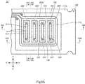
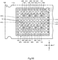
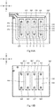
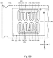
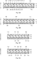
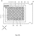
- a capacitive sensor S1 (which may be referred to simply as a sensor S1) according to a plurality of embodiments, including a first embodiment and variants thereof, of the invention, with reference to Figs. 1A to 8H .
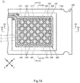
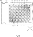
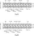
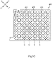
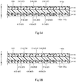
- Figs. 1A to 3C show the sensor S1 of the first embodiment.
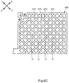
- Figs. 4A to 6C show a first variant of the sensor S1 of the first embodiment.
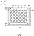
- Figs. 7A and 7B show a second variant of the sensor S1 of the first embodiment.
- Figs. 8A to 8H show third to tenth variants of the sensor S1 of the first embodiment.
- Figs. 2A to 2D and Figs. 5A to 5D indicates a Z-Z' direction (first direction).
- the Z-Z' direction corresponds to a thickness direction of a substrate 100 of the sensor S1 and includes a Z direction (one side in the first direction) and a Z' direction (the other side in the first direction).
- Figs. 1A , 1B , 3A to 3C , 4A , 4B , and 6A to 8H show a Y-Y' direction (second direction) and an X-X' direction (third direction).
- the Y-Y' and X-X' directions are substantially orthogonal to the Z-Z' direction.
- the Y-Y' direction includes a Y direction (one side in the second direction) and a Y' direction (the other side in the second direction).
- the X-X' direction is only required to cross the Y-Y' direction and may be substantially orthogonal to the Y-Y' direction.
- the X-X' direction includes an X direction (one side in the third direction) and an X' direction (the other side in the third direction).
- the sensor S1 is configured to detect a touch from the Z-direction side by a detection target, such as a finger of a user, on a detection face distinguishing the detection target from a conductor deposit, such as water, that may adhere to the detection face.
- a detection target such as a finger of a user
- the sensor S1 is housed in a housing of a vehicle or an electronic device.
- the detection face may be provided in the housing, on the Z-direction side relative to the sensor S1.
- the detection face may be a face on the most Z-direction side of the substrate 100.
- the sensor S1 includes the substrate 100 mentioned above.
- the substrate 100 includes at least one layer 110.
- the or each layer 110 is insulating.
- the substrate 100 is constituted by the layer 110.
- the layer 110 is constituted by a single-phase board or a synthetic resin film, for example.
- the substrate 100 is constituted by the plurality of layers 110 laminated in the Z-Z' direction.
- the substrate 100 is constituted by a multilayer board or a multilayer film, for example, and the plurality of layers 110 are constituted by a plurality of layers, laminated in the Z-Z' direction, of the multilayer board, or alternatively a plurality of synthetic resin films, laminated in the Z-Z' direction, of the multilayer film.
- the synthetic resin film is made of, e.g., one of the following materials or a polymer alloy in which a plurality of materials is selected from the following materials and mixed: polycarbonate (PC), polystyrene (PS), cycloolefin copolymer (COC), cycloolefin polymer (COP), polymethyl methacrylate (PMMA), or polypropylene (PP).
- the substrate 100 may be flat, or may be partly or entirely bent to form a curved surface.
- the one or plurality of layers 110 have a first face 110a and a second face 110b.
- the or each layer 110 has a face on the Z-direction side and a face on the Z'-direction side.
- the first face 110a is one of the faces on the Z- and Z'-direction sides of the one or plurality of layers 110.
- the second face 110b is one of the faces on the Z- and Z'-direction sides of the one or plurality of layers 110 that is different from the first face 110a.
- the second face 110b may be one of the faces on the Z- and Z'-direction sides of the one or plurality of layers 110 that is located on the Z'-direction side relative to the first face 110a.
- the one or plurality of layers 110 may further include a plurality of through-hole electrodes (not shown). The plurality of through-hole electrodes can be omitted.
- the layers 110 may further include a third face 110c, in addition to the first face 110a and the second face 110b.
- the third face 110c is one of the faces on the Z- and Z'-direction sides of the layers 110 that is different from, and located on the Z'-direction side relative to, the first face 110a and the second face 110b.
- the sensor S1 further includes a detection electrode 200.
- the detection electrode 200 serves dual functions of a detection electrode for self-capacitive sensing and a detection electrode for mutual capacitive sensing.
- the detection electrode 200 includes a plurality of first detection lines 210 electrically connected to each other.
- the first detection lines 210 are made of an electrically conductive material.
- the first detection lines 210 may be: (a) constituted by a conductor formed on the first face 110a of the substrate 100 by a well-known printing method, photolithography, or other means; or (b) formed by forming a conductor on the first face 110a of the substrate 100 by spattering, electroless plating, or vapor deposition and thereafter removing unnecessary portions of the conductor by laser etching or chemical etching.
- the first detection lines 210 may extend straight in the Y-Y' direction, or may curve party or entirely but extend generally in the Y-Y' direction.
- the Y-Y' direction may be, but is not required to be, a direction in which a conductor deposit adhering to the detection face falls under its own weight (where the conductor deposit is water, a direction in which the water moves under its own weight).
- the first detection lines 210 are arrayed at spaced intervals in the X-X' direction on the first face 110a of the substrate 100.
- the Y-Y' direction corresponds to the longitudinal direction of the first detection lines 210
- the X-X' direction corresponds to an array direction of the first detection lines 210.
- the sensor S1 further includes a drive electrode 300.
- the drive electrode 300 is a drive electrode for mutual capacitive sensing.
- the drive electrode 300 includes a plurality of first drive lines 310 electrically connected to each other.
- the first drive lines 310 are made of a material that is the same or similar to that of the first detection lines 210.
- the first drive lines 310 may extend straight in the Y-Y' direction, or may curve party or entirely but extend generally in the Y-Y' direction.
- the first drive lines 310 are arranged on one of the first face 110a and the second face 110b of the substrate 100 and each located between adjacent two of the first detection lines 210 as viewed from the Z-direction side.
- the first drive lines 310 and the first detection lines 210 are arranged alternately one after the other in the X-X' direction as viewed from the Z-direction side.
- the first drive lines 310 are provided on the first face 110a (see Figs. 8B, 8D , 8E, and 8G )
- each of the first drive lines 310 is spaced from corresponding adjacent two of the first detection lines 210. Accordingly, the first drive lines 310 are not electrically connected to any of first detection lines 210.
- the first drive lines 310 are provided on the second face 110b (see Figs.
- the first drive lines 310 are provided on the second face 110b, which is different from the first face 110a on which the first detection lines 210 are provided. Accordingly, the first drive lines 310 are not electrically connected to any of the first detection lines 210.
- Figs. 8B, 8D , 8E, and 8G show the first detection lines 210 and the first drive lines 310 on the first face 110a in solid lines.
- Figs. 8A, 8C , 8F, and 8H show the first detection lines 210 on the first face 110a in solid lines, and the first drive lines 310 on the second face 110b in broken lines.
- the first drive lines 310 have a dimension in the Y-Y' direction that may be larger than, substantially the same as, or smaller than, that of the first detection lines 210.
- the detection electrode 200 may further include at least one second detection line 220.
- the one or plurality of second detection lines 220 are electrically connected to the plurality of first detection lines 210, but not to the plurality of first drive lines 310.
- the one or plurality of second detection lines 220 are made of a material that is the same or similar to that of the first detection lines 210.
- the one or plurality of second detection lines 220 may extend straight in the X-X' direction, or may curve party or entirely but extend generally in the X-X' direction.
- the one or plurality of second detection lines 220 are arranged on one of the first face 110a and the second face 110b of the substrate 100.
- the one or plurality of second detection lines 220 may have one of the following configurations (1) to (4).
- Figs. 8A to 8D show the second detection lines 220 on the first face 110a are shown in solid lines
- Figs. 8E to 8H show the second detection lines 220 on the second face 110b in broken lines.
- the or each second drive line 320 has a dimension in the X-X' direction that may be larger than, substantially the same as, or smaller than, that of the at least one second detection line 220.
- the drive electrode 300 may further include at least one third drive line 330.
- the one or plurality of third drive lines 330 are electrically connected to the plurality of first drive lines 310 and the one or plurality of second drive lines 320, but not to the plurality of first detection lines 210 nor the one or plurality of second detection lines 220.
- the one or plurality of third drive lines 330 are made of a material that is the same or similar to that of the first detection lines 210.
- the third drive line 330 is arranged on the second face 110b of the substrate 100 such as to extend generally along, and overlap as viewed from the Z-direction side, one of the first detection lines 210.
- the third drive lines 330 are arranged on the second face 110b of the substrate 100 such as to extend generally along, and overlap as viewed from the Z-direction side, the respective first detection lines 210.
- the third drive lines 330 and the first drive lines 310 are arranged alternately one after the other in the array direction thereof (X-X' direction).
- the or each third drive line 330 may, but is not required to, has a width dimension (dimension in the X-X' direction) that is substantially the same as that of the overlapping first detection line 210.
- the one or plurality of third drive lines 330 are arranged away from the one or plurality of second detection lines 220 on the second face 110b.
- the or each third drive line 330 has a dimension in the Y-Y' direction that may be larger than, substantially the same as, or smaller than, that of the overlapping first detection line 210.
- the drive electrode 300 may further include at least one fourth drive line 340.
- the at least one second detection line 220 is arranged on the first face 110a of the substrate 100.
- the one or plurality of fourth drive lines 340 are electrically connected to the plurality of first drive lines 310, the one or plurality of second drive lines 320, and the one or plurality of third drive lines 330, but not to the plurality of first detection lines 210 nor the one or plurality of second detection lines 220.
- the one or plurality of fourth drive lines 340 are made of a material that is the same or similar to that of the first detection lines 210.
- the fourth drive line 340 is arranged on the second face 110b of the substrate 100 such as to extend generally along the second detection line 220 or one of the second detection lines 220, overlap the second detection line 220 or the one second detection line 220 as viewed from the Z-direction side.
- the fourth drive line 340 intersects at least the one or plurality of third drive lines 330 and is electrically connected to the one or plurality of third drive lines 330 at the intersection or intersections.
- the fourth drive lines 340 are arranged on the second face 110b of the substrate 100 such as to extend along, and overlap as viewed from the Z-direction side, the respective second detection lines 220.
- the fourth drive lines 340 intersect at least the one or plurality of third drive lines 330 and are electrically connected to the one or plurality of third drive lines 330 at the intersections.
- the or each fourth drive line 340 may, but is not required to, have a width dimension (dimension in the Y-Y' direction) that is substantially the same as that of the overlapping second detection line 220.
- the or each fourth drive line 340 has a dimension in the X-X' direction that that may be larger than, substantially the same as, or smaller than, that of the overlapping second detection line 220.
- the plurality of first detection lines 210 and the second detection lines 220 may mutually intersect forming a mesh pattern on the first face 110a, and the first drive lines 310, the second drive lines 320, the third drive lines 330, and the fourth drive lines 340 may be arranged to form a mesh pattern on the second face 110b ( Figs. 1A to 3C ).
- each of the first drive lines 310 is located between adjacent two of the first detection lines 210 as viewed from the Z-direction side
- each of the second drive lines 320 is located between adjacent two of the second detection lines 220 as viewed from the Z-direction side.
- the first drive lines 310 and the third drive lines 330 are arranged alternately one after the other in the array direction thereof (X-X' direction)
- the second drive lines 320 and the fourth drive lines 340 are arranged alternately one after the other in the array direction thereof (Y-Y' direction).
- the mesh constituted by the first detection lines 210 and the second detection lines 220 as viewed from the Z direction has a plurality of clearances, each of which include four spaces S. In other words, there are a plurality of sets of four spaces S.
- the four spaces S of each set are defined by adjacent two of the first detection lines 210, adjacent two of the second detection lines 220 that intersect the adjacent two first detection lines 210, one of the first drive lines 310 that is located between the adjacent two first detection lines 210, and one of the second drive lines 320 that is located between the adjacent two second detection lines 220.
- the detection electrode 200 may further include a third detection line 230 (see Figs. 1A , 3A , 4A , 6A , 7A and 7B ).
- the third detection line 230 is electrically connected to the plurality of first detection lines 210 and the one or plurality of second detection lines 220, but not to the plurality of first drive lines 310, the one or plurality of second drive lines 320, the one or plurality of third drive lines 330, nor the one or plurality of fourth drive lines 340.
- the third detection line 230 has a ring shape or a partially discontinuous ring shape, and is made of a material that is the same or similar to that of the first detection lines 210.
- the third detection line 230 is provided on the first face 110a of the substrate 100, surrounds at least the first detection lines 210, and is coupled to opposite ends in the longitudinal direction of the first detection lines 210.
- the third detection line 230 is provided on the first face 110a of the substrate 100, surrounds the first detection lines 210 and the one or plurality of second detection lines 220, and is coupled to opposite ends in the longitudinal direction of the first detection lines 210 and opposite ends in the longitudinal direction of the one or plurality of second detection lines 220 (see Figs. 3A , 6A , and 7B ).
- the third detection line 230 can be omitted.
- the drive electrode 300 may further include a fifth drive line 350 (see Figs. 1A , 3A , 4A , 6A , 7A and 7B ).
- the fifth drive line 350 has a ring shape or a partially discontinuous ring shape, and is made of a material that is the same or similar to that of the first detection lines 210.
- the fifth drive line 350 is arranged on the first face 110a of the substrate 100 and surrounds the third detection line 230.
- the fifth drive line 350 is electrically connected to the plurality of first drive lines 310, the one or plurality of second drive lines 320, the one or plurality of third drive lines 330, and the one or plurality of fourth drive lines 340, but not to the first detection lines 210, the one or plurality of second detection lines 220, and the third detection line 230.
- the fifth drive line 350 is electrically connected to the plurality of first drive lines 310, the one or plurality of second drive lines 320, the one or plurality of third drive lines 330, and/or the one or plurality of fourth drive lines 340 via the corresponding through-hole electrodes of the substrate 100.
- the fifth drive line 350 can be omitted.
- the at least one second detection line 220 can be omitted.
- the at least one second drive line 320, the at least one third drive line 330, and/or the at least one fourth drive line 340 can be omitted.
- the sensor S1 of the first embodiment and the sensor S1 of the first variant have substantially the same configuration except for the presence or absence of the plurality of third drive lines 330 and the plurality of fourth drive lines 340. As such, it is suggested to refer to Figs. 4A to 6C showing the sensor S1 of the first variant for the reference to the aspects in which the third drive lines 330 and the fourth drive lines 340 are omitted.
- the sensor S1 may further include a ground electrode 400 electrically connected to a ground of the substrate 100.
- the ground electrode 400 includes a plurality of first ground lines 410 electrically connected to each other.
- the first ground lines 410 are made of a material that is the same or similar to that of the first detection lines 210.
- the first ground lines 410 extend generally along the respective first detection lines 210. Where the at least one third drive line 330 is not provided, the first ground lines 410 are arranged on the third face 110c of the substrate 100 such as to overlap the respective first detection lines 210 as viewed from the Z-direction side.
- Each of the first ground lines 410 has a width dimension (dimension in the X-X' direction) that may be slightly larger than, substantially the same as, or smaller than, that of the overlapping first detection line 210.
- the at least one third drive line 330 include a plurality of third drive lines 330
- the first ground lines 410 are arranged on the third face 110c of the substrate 100 such as to overlap the respective first detection lines 210 and the respective third drive lines 330 as viewed from the Z-direction side.
- the width dimension (dimension in the X-X' direction) of each of the first ground lines 410 may be slightly larger than, or substantially the same as, that of each of the overlapping first detection line 210 and the overlapping third drive line 330.
- the ground electrode 400 may further include at least one second ground line 420.
- the or each second ground line 420 is made of a material that is the same or similar to that of the first detection lines 210.
- the or each second ground line 420 extends along the at least one second detection line 220, intersects the plurality of first ground lines 410, and is electrically connected to the first ground lines 410 at the intersections.
- the second ground line 420 is arranged on the third face 110c of the substrate 100 such as to overlap the single second detection line 220 or one of the second detection lines 220 as viewed from the Z-direction side.
- the at least one second ground line 420 include the plurality of second ground lines 420
- the at least one second detection line 220 include the plurality of second detection lines 220
- the plurality of fourth drive lines 340 is not provided
- the second ground lines 420 are arranged on the third face 110c of the substrate 100 such as to overlap the respective second detection lines 220 as viewed from the Z-direction side.
- the or each second ground line 420 has a width dimension (dimension in the X-X' direction) that may be slightly larger than, substantially the same as, or smaller than, that of the overlapping second detection line 220.
- the second ground line 420 includes the single second ground line 420, and the at least one fourth drive line 340 is provided
- the second ground line 420 is arranged on the third face 110c of the substrate 100 such as to overlap the single second detection line 220 and the single fourth drive line 340 as viewed from the Z-direction side, or alternatively overlap one of the second detection lines 220 and one of the fourth drive lines 340 as viewed from the Z-direction side.
- the at least one second ground line 420 include the plurality of second ground lines 420
- the at least one second detection line 220 include the plurality of second detection lines 220
- the plurality of fourth drive lines 340 are provided
- the second ground lines 420 are arranged on the third face 110c of the substrate 100 such as to overlap the respective second detection lines 220 and the respective fourth drive lines 340 as viewed from the Z-direction side.
- the width dimension (dimension in the Y-Y' direction) of the or each second ground line 420 may be slightly larger than, substantially the same as, or smaller than, that of each of the overlapping second detection line 220 and the overlapping fourth drive line 340.
- the plurality of first detection lines 210 and the plurality of second detection lines 220 mutually intersect forming a mesh pattern on the first face 110a
- the plurality of first ground lines 410 and the plurality of second ground lines 420 may also mutually intersect forming a mesh pattern on the third face 110c (see Figs. 1A to 7B ).
- the first ground lines 410 and/or the at least one second ground line 420 can be omitted.
- the third face 110c of the substrate 100 can also be omitted.
- the plurality of first ground lines 410 and the plurality of second ground lines 420 intersecting in a mesh pattern may be constituted by the conductor described above or by a mesh-patterned metal plate, similarly to the first detection lines 210 and the second detection lines 220 intersecting in a mesh pattern.
- the mesh constituted by the first ground lines 410 and the second ground lines 420 has a plurality of clearances (second clearances) being a plurality of gaps G (see Figs. 3C and 6C ).
- Each gap G is defined by adjacent two of the first ground lines 410, and adjacent two of the second ground lines 420 that intersect the adjacent two first ground lines 410.
- Each gap G is located on the Z'-direction side relative to the four spaces S of the corresponding set (see Figs. 1B and 4B ).
- the ground electrode 400 may further include a third ground line 430.
- the third ground line 430 has a ring shape or a partially discontinuous ring shape, and is made of a material that is the same or similar to that of the first detection lines 210.
- the third ground line 430 is arranged on the first face 110a of the substrate 100 such as to surround the fifth drive line 350 (see Figs. 7A and 7B ).
- the third ground line 430 is provided on the first face 110a of the substrate 100 and surrounds at least the first detection lines 210.
- the third ground line 430 can be omitted (see Figs. 1A to 6C ).
- the sensor S1 may further include a controller 500.
- the controller 500 is only required to be constituted by a logic circuit, such as a detection IC, software to processed by a processor, or the like and electrically connected to the detection electrode 200 and the drive electrode 300.
- the controller 500 may be, but is not required to be, mounted on the substrate 100 or provided in the substrate 100.
- the controller 500 is configured to charge and discharge the detection electrode 200 and supply drive pulses to the drive electrode 300. When a detection target approaches the detection electrode 200 while the detection electrode 200 is being charged and discharged, the approach causes a change in a first capacitance between the detection electrode 200 and the detection target.
- the approach causes a change in a second capacitance between the detection electrode 200 and the drive electrode 300.
- the controller 500 is further configured to detect the detection target on the basis of changes in the first and second capacitances.
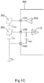
- the controller 500 may include an internal capacitor CADC, an analog-to-digital converter (ADC) 510, an I/O port 520, an external pin 530, an external pin 540, and an external pin 550, for example (see Fig. 1C ).
- the internal capacitor CADC may be connected to the external pins 530 and 540.
- the external pin 540 may be connected to the ground of the substrate 100.
- the external pin 530 may be connected to the detection electrode 200, and an external capacitor CRX may be provided between the detection electrode 200 and the ground.
- the I/O port 520 may be connected to the drive electrode 300 via the external pin 550, and drive pulses may be supplied to the drive electrode 300 from the I/O port 520.
- a mutual capacitance CTXRX (which may be referred to as a second capacitance CTXRX) is formed between the drive electrode 300 and the detection electrode 200.
- the controller 500 includes a memory (not shown), which stores first and second threshold values.
- the second capacitance CTXRX includes at least a first mutual capacitance. Since each of the first drive lines 310 of the drive electrode 300 is located between adjacent two of the first detection lines 210 of the detection electrode 200 as viewed from the Z-direction side, during drive pulses supply, a first mutual capacitance is formed between the first drive lines 310 and the first detection lines 210 adjacent thereto.
- the second capacitance CTXRX further includes a second mutual capacitance, a third mutual capacitance, and a fourth mutual capacitance.
- a second mutual capacitance is formed between the second drive lines 320 and the second detection lines 220 adjacent thereto, a third mutual capacitance is formed between the first drive lines 310 and portions on the X- and X'-direction sides relative to a plurality of intersecting portions of the plurality of second detection lines 220, and a fourth mutual capacitance is formed between the second drive lines 320 and portions on the Y- and Y'-direction sides relative to a plurality of intersecting portions of the plurality of first detection lines 210.
- the intersecting portions of the second detection lines 220 are portions of the second detection lines 220 where the second detection lines 220 intersects the first drive lines 310 as viewed from the Z direction.
- the intersecting portions of the first detection lines 210 are portions of the first detection lines 210 where the first detection lines 210 intersect the second drive lines 320 as viewed from the Z direction.
- the second capacitance CTXRX further includes a fifth mutual capacitance. Since the fifth drive line 350 surrounds the third detection line 230 in spaced relation to each other, During drive pulses supply, a fifth mutual capacitance is formed between the third detection line 230 and the fifth drive line 350.
- the second capacitance CTXRX further includes a sixth mutual capacitance.
- each of the first drive lines 310 includes first and second portions located on the Y- and Y'-direction sides, respectively, relative to the third detection line 230 (the first and second portions of each first drive line 310 are located outside the third detection line 230).
- a sixth mutual capacitance is formed between the third detection line 230 and the first and second portions of first drive lines 310.
- the second capacitance CTXRX further includes a seventh mutual capacitance.
- the or each second drive line 320 includes first and second portions located on the X- and X'-direction sides, respectively, relative to the third detection line 230 (the first and second portions of the or each second drive line 320 are located outside the third detection line 230).
- a seventh mutual capacitance is formed between the third detection line 230 and the first and second portions of the at least one second drive line 320.
- the second capacitance CTXRX further includes an eighth mutual capacitance.
- the or each third drive line 330 includes first and second portions located on the Y- and Y'-direction sides, respectively, relative to the third detection line 230 (the first and second portions of the or each third drive line 330 are located outside the third detection line 230).
- an eighth mutual capacitance is formed between the third detection line 230 and the first and second portions of the at least one third drive line 330.
- the second capacitance CTXRX further includes a ninth mutual capacitance.
- the or each fourth drive line 340 includes first and second portions located on the X- and X'-direction sides, respectively, relative to the third detection line 230 (the first and second portions of the or each fourth drive line 340 are located outside the third detection line 230).
- a ninth mutual capacitance is formed between the third detection line 230 and the first and second portions of the at least one fourth drive line 340.
- the controller 500 is configured to supply drive pulses to the drive electrode 300 and repeat the following process steps (A) to (D).
- the signal of the drive pulses is at a low level in step (A) above, changes from the low level to a high level in step (B) above, is maintained at the high level in step (C) above, and changes from the high level to the low level in step (D) above.
- the voltage of the internal capacitor CADC input into the ADC 510 is increased compared to a case where the drive pulses are not supplied.
- the voltage of the internal capacitor CADC input to the ADC 510 is decreased compared to the case where the drive pulse is not supplied.
- the first capacitance between the detection target and the detection electrode 200 is added to the external capacitor CRX, whereas the electric charge of the second capacitance CTXRX between the drive electrode 300 and the detection electrode 200 moves to earth through the detection target, so that the second capacitance CTXRX decreases.
- the voltage of the internal capacitor CADC decreases as the first capacitance increases, and the voltage of the internal capacitor CADC decreases as the second capacitance CTXRX decreases.
- the voltage of the internal capacitor CADC decreases in accordance with both a change in the first capacitance and a change in the second capacitance CTXRX.
- the voltage of the internal capacitor CADC is significantly decreased compared to a case where the voltage of the internal capacitor CADC is decreased in accordance with a change in the first capacitance only or a change in the second capacitance CTXRX only.
- the voltage of the internal capacitor CADC increases as the first capacitance increases, and the voltage of the internal capacitor CADC increases as the second capacitance CTXRX decreases.
- the voltage of the internal capacitor CADC increases in accordance with both a change in the first capacitance and a change in the second capacitance CTXRX.
- the voltage of the internal capacitor CADC is significantly increased as compared to the case where the voltage of the internal capacitor CADC is increased in accordance with a change in the first capacitance only or a change in the second capacitance CTXRX only.
- the controller 500 is configured to compare the voltage of the internal capacitor CADC at the first timing with the first threshold value, and makes a first determination of whether or not the voltage of the internal capacitor CADC at the first timing is equal to or smaller than the first threshold value.
- the controller 500 compares the voltage of the internal capacitor CADC at the second timing with the second threshold value, and makes a second determination of whether or not the voltage of the internal capacitor CADC at the second timing is equal to or larger than the second threshold value.
- controller 500 determines that the voltage of the internal capacitor CADC is equal to or smaller than the first threshold value as a result of the first determination and/or determines that the voltage of the internal capacitor CADC is equal to or larger than the second threshold value as a result of the second determination, then the controller 500 determines that the detection target has touched the detection face.
- the first capacitance between the conductor deposit and the detection electrode 200 is added to the external capacitor CRX. Since the conductor deposit electrically floats from earth, the capacitance of the conductor deposit is added to second capacitance CTXRX between the drive electrode 300 and the detection electrode 200, and accordingly the second capacitance CTXRX increases by the capacitance of the conductor deposit.
- the voltage component of the internal capacitor CADC that should decrease as the first capacitance increases is cancelled by the voltage component of the internal capacitor CADC that should increase as the second capacitance CTXRX increases.
- Such cancellation results in that the voltage of the internal capacitor CADC changes hardly or slightly at the first timing.
- the voltage component of the internal capacitor CADC that should increase as the first capacitance increases is cancelled by the voltage component of the internal capacitor CADC that should decrease as the second capacitance CTXRX increases.
- the controller 500 will not erroneously determine that the conductor deposit is a detection target in the results of the first and/or second determinations.
- the controller 500 is thus able to detect a touch on the detection face by the detection target distinguishing the detection target from the conductor deposit.
- the spacing between the first drive lines 310 in the X-X' direction may be adjusted such that the first capacitance is substantially the same as the second capacitance CTXRX.
- the second capacitance CTXRX can be decreased, by reducing the spacing between the first drive lines 310 of the drive electrode 300 in the X-X' direction, such that the first capacitance is substantially the same as the second capacitance CTXRX.
- the spacing between the first drive lines 310 in the X-X' direction may be smaller than the spacing between the first detection lines 210 in the X-X' direction.
- the second capacitance CTXRX is larger than the first capacitance. More particularly, the second capacitance CTXRX is can be increased, by enlarging the spacing between the first drive lines 310 of the drive electrode 300 in the X-X' direction, such that the first capacitance is substantially the same as the second capacitance CTXRX
- the spacing between the first drive lines 310 in the X-X' direction and the spacing between the second drive lines 320 in the Y-Y' direction may be adjusted such that the first capacitance is substantially the same as the second capacitance CTXRX.
- the second capacitance CTXRX can be decreased, by reducing the spacing between the first drive lines 310 of the drive electrode 300 in the X-X' direction and the spacing between the second drive lines 320 in the Y-Y' direction, such that the first capacitance is substantially the same as the second capacitance CTXRX.
- the spacing between the first drive lines 310 in the X-X' direction may be smaller than the spacing between the first detection lines 210 in the X-X' direction
- the spacing between the second drive lines 320 in the Y-Y' direction may be smaller than the spacing between the second detection lines 220 in the Y-Y' direction.
- the second capacitance CTXRX can be increased, by enlarging the spacing between the first drive lines 310 of the drive electrode 300 in the X-X' direction and the spacing between the second drive lines 320 in the Y-Y' direction, such that the first capacitance is substantially the same as the second capacitance CTXRX
- the sensor S1 as described above provides the following technical features and effects.
- Each of the first drive lines 310 of the drive electrode 300 is located between adjacent two of the first detection lines 210 of the detection electrode 200 as viewed from the Z-direction side.
- a conductor deposit adhering to the detection face is located substantially on the Z-direction side relative to at least one of the first drive lines 310 and the first detection line(s) 210 adjacent thereto, making it possible to change the first mutual capacitance of the second capacitance CTXRX, formed between the at least one of the first drive lines 310 and the first detection line(s) 210 adjacent thereto.
- Such change in the first mutual capacitance increases the possibility that the conductor deposit adhering to the detection face changes the second capacitance CTXRX, thereby reducing the possibility that the controller 500 erroneously detects the conductor deposit as a detection target.
- each of the first drive lines 310 is located between adjacent two of the first detection lines 210 of the detection electrode 200 as viewed from the Z-direction side
- each of the second drive lines 320 is located between adjacent two of the second detection lines 220 as viewed from the Z-direction side
- a conductor deposit adhering to the detection face is located substantially on the Z-direction side relative to at least one of the first drive lines 310 and the first detection line(s) 210 adjacent thereto and/or at least one of the second drive lines 320 and the second detection line(s) 220 adjacent thereto, making it possible to change the first, second, third, and/or fourth mutual capacitance of the second capacitance CTXRX.
- the first mutual capacitance is formed between the at least one of the first drive lines 310 and the first detection line(s) 210 adjacent thereto
- the second mutual capacitance is formed between the at least one of the second drive lines 320 and the second detection line(s) 220 adjacent thereto.
- the third mutual capacitance is between each of the first drive lines 310 and the portions on the X- and X'-direction sides relative to the intersecting portions of the second detection lines 220.
- the fourth mutual capacitance is formed between each of the second drive lines 320 and the potions on the Y- and Y'-direction sides relative to the intersecting portions of the first detection lines 210.
- Such change(s) in the mutual capacitance(s) increases the possibility that the conductor deposit adhering to the detection face further changes the second capacitance CTXRX, thereby further reducing the possibility that the controller 500 erroneously detects the conductor deposit as a detection target.
- a conductor deposit adhering to the detection face is located substantially on the Z-direction side relative to the fifth drive line 350 and the third detection line 230, making it possible to change the fifth mutual capacitance of the second capacitance CTXRX, formed between the fifth drive line 350 and the third detection line 230.
- Such change in the fifth mutual capacitance increases the possibility that the conductor deposit adhering to the detection face changes the second capacitance CTXRX, thereby further reducing the possibility that the controller 500 erroneously detects the conductor deposit as a detection target.
- the plurality of first drive lines 310, the at least one second drive line 320, the at least one third drive line 330, and/or the at least one fourth drive lines 340 of the drive electrode 300 each include the first and second portions located outside the third detection line 230
- a conductor deposit adhering to the detection face is located substantially on the Z-direction side relative to the first and/or second portions of at least one of the first drive lines 310, the second drive line(s) 320, the third drive line(s) 330 and/or the fourth drive line(s) 340 and the third detection line 230, making it possible to change the sixth, seventh, eighth, and/or nineth mutual capacitance of the second capacitance CTXRX.
- the sixth mutual capacitance is formed between the third detection line 230 and the first and/or second portions of the the at least one first drive lines 310.
- the seventh mutual capacitance is formed between the third detection line 230 and the first and/or second portions of the at least one second drive line 320.
- the eighth mutual capacitance is formed between the third detection line 230 and the first and/or second portions of the at least one third drive line 330.
- the ninth mutual capacitance is formed between the third detection line 230 and the first and/or second portions of the at least one fourth drive line 340.
- Such change(s) in the mutual capacitance(s) increases the possibility that the conductor deposit adhering to the detection face changes the second capacitance CTXRX, thereby further reducing the possibility that the controller 500 erroneously detects the conductor deposit as a detection target.
- the at least one third drive line 330 is provided, the or each third drive line 330 on the second face 110b of the substrate 100 overlaps a corresponding one of the first detection lines 210 on the first face 110a of the substrate 100 and thereby functions as an electromagnetic shield to shield the corresponding first detection line 210 from the Z'-direction side. Therefore, the at least one first detection line 210 is less susceptible to electromagnetic influence from the Z'-direction side.
- the or each fourth drive line 340 on the second face 110b of the substrate 100 overlaps the second detection line 220 or a corresponding one of the second detection lines 220 on the first face 110a of the substrate 100 and thereby functions as an electromagnetic shield to shield the corresponding second detection line 220 from the Z'-direction side. Therefore, the at least one second detection line 220 is less susceptible to electromagnetic influence from the Z'-direction side.
- the or each first ground line 410 on the third face 110c of the substrate 100 overlaps a corresponding one of the first detection lines 210 on the first face 110a of the substrate 100 and thereby functions as an electromagnetic shield to shield the corresponding first detection line 210 from the Z'-direction side. Therefore, the at least one first detection line 210 is less susceptible to electromagnetic influence from the Z'-direction side.
- the or each second ground line 420 on the third face 110c of the substrate 100 overlaps the second detection line 220 or a corresponding one of the second detection lines 220 on the first face 110a or the second face 110b of the substrate 100 and thereby functions as an electromagnetic shield to shield the corresponding second detection line 220 from the Z'-direction side. Therefore, the at least one second detection line 220 is less susceptible to electromagnetic influence from the Z'-direction side.
- part of the electric charge from the first and second drive lines 310 and 320 does not move to the plurality of gaps G but to the adjacent first and second detection lines 210 and 220, suppressing the reduction in the first to fourth mutual capacitances.
- a capacitive sensor S2 (which may be referred to simply as a sensor S2) according to a plurality of embodiments, including a second embodiment and variants thereof, of the invention, with reference to Figs. 9A to 11C.
- Figs. 9A to 11C show the sensor S2 of the second embodiment.
- Figs. 10A to 10D also show the Z-Z' direction as in the sensor S1.
- Figs. 9A and 9B and Figs. 11A to 11C also show the X-X' and Y-Y' directions as in the sensor S1.
- the sensor S2 has a configuration similar to that of the sensor S1 but different in the following points: (1) a detection electrode 200' includes a plurality of first detection lines 210 and a pair of second detection lines 220 on a first face 110a of a substrate 100; and (2) a drive electrode 300' includes a plurality of first drive lines 310 on the first face 110a of the substrate 100 and a second drive line 320' on a second face 110b of the substrate 100. These differences will be described in detail, omitting descriptions of the sensor S2 on overlaps with the sensor S1.
- the plurality of first detection lines 210 of the detection electrode 200' extend in the Y-Y' direction and are arrayed at spaced intervals in the X-X' direction (see Figs. 9A and 11A ).
- the first detection lines 210 each have a first end on the Y-direction side and a second end on the Y'-direction side.
- the first detection lines 210 include a first detection line 210 on the X-direction side and a first detection line 210 on the X'-direction side.
- the first detection line 210 on the X-direction side is the one of the first detection lines 210 that is located on the most X-direction side.
- the first detection line 210 on the X'-direction side is the one of the first detection lines 210 that is located on the most X'-direction side.
- the pair of second detection lines 220 of the detection electrode 200' includes one and the other of the second detection lines 220.
- the one second detection line 220 extends in the X-X' direction and is coupled to the first ends of the first detection lines 210.
- the other second detection line 220 extends in the X-X' direction and is coupled to the second ends of the first detection lines 210.
- the first detection line 210 on the X-direction side, the first detection line 210 on the X'-direction side, and the pair of second detection lines 220 form a detection line of generally rectangular ring shape. This detection line may be referred to as a "ring-shaped detection line". It should be noted that only one of the pair of second detection lines 220 may be provided.
- the plurality of first drive lines 310 of the drive electrode 300' extend in the Y-Y' direction.
- Each of the first drive lines 310 is arranged between adjacent two of the first detection lines 210 as viewed from the Z-direction side.
- the first drive lines 310 each have a first end in the Y direction and a second end in the Y' direction.
- Each of the first drive lines 310 has a dimension in the Y-Y' direction that is smaller than that of each of the first detection lines 210.
- the first ends of the first drive lines 310 are spaced from the one second detection line 220 in the Y-Y' direction, and the second ends of the first drive lines 310 are spaced from the other second detection line 220 in the Y-Y direction. Accordingly, the first drive lines 310 are not electrically connected to the second detection lines 220.
- the drive electrode 300' may further include the fifth drive line 350 described above.
- the fifth drive line 350 surrounds the ring-shaped detection line in spaced relation to each other on the first face 110a of the substrate 100.
- the fifth drive line 350 can be omitted.
- the second drive line 320' of the drive electrode 300' includes a main body 321' having a ring shape or a partially discontinuous ring shape.
- the main body 321' includes a first portion 321a' and/or a second portion 321b'. Where the first portion 321a' is provided, the first portion 321a' is an inner perimeter portion of the main body 321' and is located such as to overlap the ring-shaped detection line as viewed from the Z-direction side, and the second portion 321b' is a portion of the main body 321' that has a ring shape or a partially discontinuous ring shape and is located outside the first portion 321a' of the main body 321' and outside the ring-shaped detection line.
- the second portion 321b' is a portion of the main body 321' that has a ring shape or a partially discontinuous ring shape and is located outside the ring-shaped detection line.
- the fifth drive line 350 is provided, whether or not the first portion 321a' is provided, the second portion of the main body 321' is located between the fifth drive line 350 and the ring-shaped detection line as viewed from the Z-direction side.
- the main body 321' is connected to the fifth drive line 350 via a through-hole electrode of the substrate 100. The second portion of the main body 321' can be omitted.
- the second drive line 320' may further include a plurality of first connecting portions 322' and a plurality of second connecting portions 323'.
- the substrate 100 include a plurality of through-hole electrodes 130 and a plurality of through-hole electrodes 140.
- Each first connecting portion 322' extends in the Y' direction, from a portion on the Y-direction side of the first portion 321a' of the main body 321' to a position on the Z'-direction side relative to the first end of a corresponding one of the first drive lines 310.
- the distal end of each first connecting portion 322' is connected to the first end of the corresponding first drive line 310 via a corresponding one of the through-hole electrodes 130 of the substrate 100.
- each first connecting portions 322' is arranged between adjacent two of the first detection lines 210 and also between the first end of the corresponding first drive line 310 and the one second detection line 220.
- Each second connecting portion 323' extends in the Y direction, from a portion on the Y'-direction side of the first portion 321a' of the main body 321' to a position on the Z'-direction side relative to the second end of a corresponding one of the first drive lines 310.
- the distal end of the second connecting portion 323' is connected to the second end of the corresponding first drive line 310 via a corresponding one of the corresponding through-hole electrodes 140 of the substrate 100.
- each second connecting portion 323' is arranged between adjacent two of the first detection lines 210 and also between the second end of the corresponding first drive line 310 and the other second detection line 220.
- the first drive lines 310 may be provided not on the first face 110a of the substrate 100, but on the second face 110b of the substrate 100.
- the first connecting portions 322' and the second connecting portions 323' can be omitted, and the first and second ends of the first drive lines 310 may extend to, and be coupled to, the main body 321'.
- two elongated spaces S exist between adjacent two of the first detection lines 210 and one of the first drive lines 310 that is located between the adjacent two first detection lines as viewed from the Z direction.
- the two spaces S exist for each set of the two adjacent first detection lines 210. In other words, there is a plurality of sets of the two spaces S.
- the drive electrode 300' may further include at least one third drive line 330.
- the or each third drive line 330 extends from the portion on the Y-direction side to the portion on the Y'-direction side of the first portion 321a' of the main body 321'.
- the one or plurality of third drive lines 330 of the drive electrode 300' is arranged on the second face 110b of the substrate 100 such as to extend along, and overlap as viewed from the Z-direction side, the one or plurality of first detection lines 210.
- the at least one third drive line 330 can be omitted.
- the sensor S2 may further include a ground electrode 400' electrically connected to a ground of the substrate 100.
- the ground electrode 400' may include the plurality of first ground lines 410 and/or the at least one second ground line 420 described above.
- the at least one second ground line 420 may include two second ground lines 420 arranged such as to each overlap one of the pair of second detection lines 220.
- the two second ground lines 420 include a second ground line 420 on the Y-direction side and a second ground line 420 on the Y'-direction side.
- the ground electrode 400' may further include at least one fourth ground line 440 electrically connected to at least the plurality of first ground lines 410.
- the least one fourth ground line 440 is made of a material that is the same or similar to that of the first detection lines 210.
- the at least one fourth ground line 440 is arranged on the third face 110c of the substrate 100 such as to extend along, and overlap as viewed from the Z-direction side, at least one of the first drive lines 310.
- the at least one fourth ground line 440 may include a plurality of fourth ground lines 440 arranged on the third face 110c of the substrate 100 such as to overlap the corresponding first drive lines 310. In this case, the fourth ground lines 440 and the first ground lines 410 are arranged alternately one after the other in the X-X' direction.
- the ground electrode 400' may include a plurality of sixth ground lines 460 and a plurality of seventh ground lines 470.
- the sixth ground lines 460 and the seventh ground lines 470 are made of a material that is the same or similar to that of the first detection lines 210.
- the sixth ground lines 460 are provided on the third face 110c of the substrate 100, extend in the Y-Y' direction, and arrayed at spaced intervals in the X-X' direction.
- the seventh ground lines 470 are provided on the third face 110c of the substrate 100, extend in the X-X' direction, and are arrayed at spaced intervals in the Y-Y' direction.
- the sixth ground lines 460 and the seventh ground lines 470 mutually intersect forming a mesh pattern and are mutually connected electrically at the intersections.
- the sixth ground lines 460 include the plurality of first ground lines 410 and the at least one fourth ground line 440, and the plurality of seventh ground lines 470 include the at least one second ground line 420.
- the plurality of through-hole electrodes 130 and the plurality of through-hole electrodes 140 of the substrate 100 may reach the third face 110c of the substrate 100 (see Fig. 10D ).
- the ground electrode 400' may further include a plurality of fifth ground lines 450 generally of ring shape, made of a material that is the same or similar to that of the first detection lines 210.
- Each of the fifth ground lines 450 is arranged on the third face 110c of the substrate 100 such as to be located between, and coupled to, adjacent two of the plurality of first ground lines 410.
- the fifth ground lines 450 include a plurality of fifth ground lines 450 on the Y-direction side, each surrounding one of the through-hole electrodes 130, and a plurality of fifth ground lines 450 on the Y'-direction side, each surrounding one of the through-hole electrodes 140.
- the fifth ground lines 450 on the Y-direction side are located on the Y'-direction side adjacently to, and coupled to, the second ground line 420 on the Y-direction side.
- the fifth ground lines 450 on the Y-direction side divide, and are coupled to, one of the seventh ground lines 470 that is located on the Y'-direction side relative to the second ground line 420 on the Y-direction side.
- the fifth ground lines 450 on the Y'-direction side are located on the Y-direction side adjacently to, and coupled to, the second ground line 420 on the Y'-direction side.
- the fifth ground lines 450 on the Y'-direction side divide, and are coupled to, one of the seventh ground lines 470 that is located on the Y-direction side relative to the second ground line 420 on the Y'-direction side.
- each of the fifth ground lines 450 on the Y-direction side and each of the fifth ground lines 450 on the Y'-direction side divide, and are coupled to, a corresponding one of the fourth ground lines 440.
- the ground electrode 400' may further include the third ground line 430 described above as in the ground electrode 400 of the sensor S1.
- an elongated gap may be provided to extend between, and along, each adjacent two of the first ground lines 410.
- each gap is located on the Z'-direction side relative to the two spaces S of the corresponding set.
- an elongated gap may be provided to extend between, and along, each of the fourth ground lines 440 and one of the first ground lines 410 that is adjacent to the fourth ground line 440.
- Each gap exists for each set of the adjacent fourth ground line 440 and first ground line 410.
- Each gap is located on the Z'-direction side relative to a corresponding one of the spaces S.
- the mesh constituted by the sixth ground lines 460 and the seventh ground lines 470 has a plurality of clearances being a plurality of gaps.
- Each gap is defined by adjacent two of the sixth ground lines 460 and adjacent two of the seventh ground lines 470 which intersect the adjacent two sixth ground lines 460.
- the gaps in the mesh include a plurality of sets of gaps G, and the gap G of each set is located between adjacent two of the first ground lines 410 and fourth ground lines 440 of the sixth ground lines 460.
- Each gap G is located on the Z'-direction side relative to a corresponding one of the spaces S.
- a controller 500 of the sensor S2 is configured to charge and discharge the detection electrode 200' and supply drive pulses to the drive electrode 300'.
- the approach causes a change in a first capacitance between the detection electrode 200' and the detection target.
- the approach causes a change in a second capacitance between the detection electrode 200' and the drive electrode 300'.
- the controller 500 of the sensor S2 is further configured to detect the detection target on the basis of the change in the first capacitance between the detection electrode 200' and the detection target and the change in the second capacitance between the detection electrode 200' and the drive electrode 300'.
- a second capacitance CTXRX of the sensor S2 includes at least a first mutual capacitance as described above. Where the second portion 321b' of the main body 321' of the second drive line 320' is arranged outside the ring-shaped detection line, the second capacitance CTXRX further includes a tenth mutual capacitance. During drive pulses supply, a tenth mutual capacitance is formed between the second portion 321b' of the main body 321' and the ring-shaped detection line.
- the second capacitance CTXRX further includes an eleventh mutual capacitance, a twelfth mutual capacitance, a thirteenth mutual capacitance, and a fourteenth mutual capacitance.
- an eleventh mutual capacitance is formed between the first connecting portions 322' and the first detection lines 210 adjacent thereto, a twelfth mutual capacitance is formed between the second connecting portions 323' and the first detection lines 210 adjacent thereto, a thirteenth mutual capacitance is formed between the first connecting portions 322' and the one second detection line 220, and a fourteenth mutual capacitance is formed between the second connecting portions 323' and the other second detection line 220.
- the fifth drive line 350 surrounds the ring-shaped detection line in spaced relation to each other
- the second capacitance CTXRX further includes a fifteenth mutual capacitance.
- a fifteenth mutual capacitance is formed between the fifth drive line 350 and the ring-shaped detection line.
- the sensor S2 as described above provides the following technical features and effects.
- Each of the first drive lines 310 of the drive electrode 300' is located between adjacent two of the first detection lines 210 of the detection electrode 200' as viewed from the Z-direction side.
- a conductor deposit adhering to the detection face is located substantially on the Z-direction side relative to at least one of the first drive lines 310 and the first detection line(s) 210 adjacent thereto, making it possible to change the first mutual capacitance of the second capacitance CTXRX, formed between the at least one of the first drive lines 310 and the first detection line(s) 210 adjacent thereto.
- Such change in the first mutual capacitance increases the possibility that the conductor deposit adhering to the detection face changes the second capacitance CTXRX, thereby reducing the possibility that the controller 500 erroneously detects the conductor deposit as a detection target.
- the conductor deposit adhering to the detection face is located substantially on the Z-direction side relative to the second portion 321b' of the main body 321' of the second drive line 320' and the ring-shaped detection line, making it possible to change the tenth mutual capacitance of the second capacitance CTXRX, formed between the second portion 321b' of the main body 321' and the ring-shaped detection line.
- Such change in the tenth mutual capacitance increases the possibility that the conductor deposit adhering to the detection face changes the second capacitance CTXRX, thereby reducing the possibility that the controller 500 erroneously detects the conductor deposit as a detection target.
- a conductor deposit adhering to the detection face is located substantially on the Z-direction side relative to at least one of the first and second connecting portions 322' and 323', making it possible to change the eleventh, twelfth, thirteenth and/or fourteenth mutual capacitance of the second capacitance CTXRX.
- the eleventh mutual capacitance is formed between each of the first connecting portions 322' and the first detection line(s) 210 adjacent thereto.
- the twelfth mutual capacitance is formed between each of the second connecting portions 323' and the first detection line(s) 210 adjacent thereto.
- the thirteenth mutual capacitance is formed between each of the first connecting portions 322' and the one second detection line 220.
- a conductor deposit adhering to the detection face is located substantially on the Z-direction side relative to the fifth drive line 350 and the ring-shaped detection line, making it possible to change the fifteenth mutual capacitance of the second capacitance CTXRX, formed between the fifth drive line 350 and the ring-shaped detection line.
- Such change in the fifteenth mutual capacitance increases the possibility that the conductor deposit adhering to the detection face changes the second capacitance CTXRX, thereby reducing the possibility that the controller 500 erroneously detects the conductor deposit as a detection target.
- the first portion 321a' of the main body 321' of the second drive line 320' overlaps the ring-shaped detection line as viewed from the Z-direction side and thereby functions as an electromagnetic shield to shield the ring-shaped detection line (namely, the first detections 210 on the X- and X'-direction side and the pair of second detection lines 220) from the Z'-direction side. Therefore, the ring-shaped detection line is less susceptible to electromagnetic influence from the Z'-direction side.
- the one or plurality of third drive lines 330 on the second face 110b of the substrate 100 overlaps at least one of the first detection lines 210 on the first face 110a of the substrate 100 and thereby function an electromagnetic shield to shield the at least one first detection line 210 from the Z'-direction side. Therefore, the at least one first detection line 210 is susceptible to electromagnetic influence from the Z'-direction side.
- the plurality of fourth ground lines 440 is provided, and the plurality of gaps exits each between one of the fourth ground lines 440 and one of the first ground lines 410 that is adjacent to the fourth ground line 440, each gap is located on the Z'-direction side relative to a corresponding one of the spaces S.
- part of the electric charge from the first drive lines 310 does not move to the gaps but moves to the adjacent first detection lines 210, suppressing the reduction in the first mutual capacitance.
- the mesh constituted by the sixth ground lines 460 and the seventh ground lines 470 has the plurality of clearances being the plurality of gaps including the plurality of sets of gaps G, and the gaps G of each set is located between adjacent two of the first ground lines 410 and fourth ground lines 440, each gap G is located on the Z'-direction side relative to the corresponding space S.
- part of the electric charge from the first drive lines 310 does not move to the gaps G, suppressing the reduction in the first mutual capacitance.
- the sensor S2 exhibits the same technical feature and effect as the technical feature and effect (3) of the sensor S1.
- a capacitive sensor S3 (which may be referred to simply as a sensor S3) according to a plurality of embodiments, including a third embodiment and variants thereof, of the invention, with reference to Figs. 12A to 14C .
- Figs. 12A to 14C show the capacitive sensor S3 of the second embodiment.
- Figs. 13A to 13D also show the Z-Z' direction as in the sensor S1.
- Figs. 12A and 12B and Figs. 14A to 14C also show the X-X' and Y-Y' directions as in the sensor S1.
- the sensor S3 has a configuration similar to that of the sensor S1 but different in the following points: (1) a detection electrode 200" includes a plurality of first detection lines 210 and at least one second detection line 220 on the first face 110a of a substrate 100, and a plurality of fourth detection lines 240 on the second face 110b of the substrate 100, and that (2) a drive electrode 300" includes a plurality of first drive lines 310 on the first face 110a of the substrate 100 and a plurality of third drive lines 330 on the second face 110b of the substrate 100. These differences will be described in detail, omitting descriptions of the sensor S3 on overlaps with the sensor S1.
- the plurality of first detection lines 210 of the detection electrode 200" extend in the Y-Y' direction and are arrayed at spaced intervals in the X-X' direction (see Figs. 12A and 14A ).
- the first detection lines 210 each include a first end portion on the Y-direction side, a second end portion on the Y'-direction side, and an intermediate portion between the first and second end portions.
- the at least one second detection line 220 of the detection electrode 200" extends in the X-X' direction, intersects the intermediate portions of the first detection lines 210, and is electrically connected to the first detection lines 210 at the intersections. Where the at least one second detection line 220 include a plurality of second detection lines 220, the second detection lines 220 may be arrayed at spaced intervals in the Y-Y' direction.
- the plurality of first drive lines 310 of the drive electrode 300" extend in the Y-Y' direction.
- Each of the first drive lines 310 has a dimension in the Y-Y' direction that is smaller than that of each of the first detection lines 210.
- the first drive lines 310 are provided on the first face 110a of the substrate 100.
- the first drive lines 310 include a plurality of first drive lines 310 on the Y-direction side, each located between the first end portions of adjacent two of the first detection lines 210 as viewed from the Z-direction side, and a plurality of first drive lines 310 on the Y'-direction side, each located between the second end portions of adjacent two of the first detection lines 210 as viewed from the Z-direction side.
- the first drive lines 310 each have a first end and a second end on the opposite side, and each first end being located closer to the at least one second detection line 220 than the corresponding second end is.
- the first ends of the first drive lines 310 are located in spaced relation to the at least one second detection line 220 in the Y-Y' direction. Accordingly, the first drive lines 310 are not electrically connected to the at least one second detection line 220.
- the drive electrode 300" may further include the fifth drive line 350 described above.
- the fifth drive line 350 surrounds the plurality of first detection lines 210, the at least one second detection line 220, and the plurality of first drive lines 310 on the first face 110a of the substrate 100.
- the second ends of the first drive lines 310 are coupled to the fifth drive line 350.
- the fifth drive line 350 is arranged in spaced relation to the plurality of first detection lines 210 and the at least one second detection line 220.
- the plurality of third drive lines 330 of the drive electrode 300" is electrically connected to the plurality of first drive lines 310, but are not to the plurality of first detection lines 210 nor the at least one second detection line 220.
- the third drive lines 330 are arranged on the second face 110b of the substrate 100 such as to extend along, and overlap as viewed from the Z-direction side, the corresponding first detection lines 210.
- the third drive lines 330 each include a first end portion on the Y-direction side, a second end portion on the Y'-direction side, and an intermediate portion between the first and second end portions.
- the drive electrode 300" may further include at least one fourth drive line 340.
- the or each fourth drive line 340 is arranged on the second face 110b of the substrate 100 such as to extend generally along, overlap as viewed from the Z-direction side, the corresponding second detection line 220.
- the at least one fourth drive line 340 intersects the intermediate portions of the plurality of third drive lines 330 and is electrically connected to the plurality of third drive lines 330 at the intersections.
- the at least one fourth drive line 340, the first drive lines 310, and the third drive lines 330 are mutually connected electrically.
- the plurality of fourth detection lines 240 of the detection electrode 200" are made of a material that is the same or similar to that of the first detection lines 210, extend generally along the plurality of first drive lines 310, and are arranged such as to overlap the first drive lines 310 as viewed from the Z-direction side.
- the fourth detection lines 240 includes fourth detection lines 240 on the Y-direction side, which overlap the first drive lines 310 on the Y-direction side, and fourth detection lines 240 on the Y'-direction side, which overlap the first drive lines 310 on the Y'-direction side.
- the fourth detection lines 240 on the Y-direction side include a fourth detection line 240 on the YX-direction side, which is the most X-direction side one of the fourth detection lines 240 on the Y-direction side, and a fourth detection line 240 on the YX'-direction side, which is the most X'-direction side one of the fourth detection lines 240 on the Y-direction side.
- the fourth detection lines 240 on the Y'-direction side include a fourth detection line 240 on the Y'X-direction side, which is the most X-direction side one of the fourth detection lines 240 on the Y'-direction side, and a fourth detection line 240 on the Y'X'-direction side, which is the most X'-direction side one of the fourth detection lines 240 on the Y'-direction side.
- the plurality of fourth detection lines 240 on the Y-direction side and the first end portions of the plurality of third drive lines 330 are alternately arranged one by one at spaced intervals in the X-X' direction, and the plurality of fourth detection lines 240 on the Y'-direction side and the second end portions of the plurality of third drive lines 330 are alternately arranged one by one at spaced intervals in the X-X' direction. Accordingly, the fourth detection lines 240 are not electrically connected to the third drive lines 330.
- Each of the fourth detection lines 240 has a first end and a second end on the opposite side, and each first end being located closer to the at least one fourth drive line 340 than the corresponding second end is.
- the first ends of the fourth detection lines 240 are located in spaced relation to the at least one fourth drive line 340 in the Y-Y' direction. Accordingly, the fourth detection lines 240 are not electrically connected to the at least one fourth drive line 340.
- the fourth detection lines 240 are connected to the plurality of first detection lines 210 and the at least one second detection line 220.
- the at least one fourth drive line 340 can be omitted.
- the detection electrode 200" may further include a plurality of fifth detection lines 250 on the second face 110b of the substrate 100.
- the fifth detection lines 250 are made of a material that is the same or similar to that of the first detection lines 210 and extend in the X-X' direction.
- the fifth detection lines 250 include a fifth detection line 250 on the Y-direction side and a fifth detection line 250 on the Y'-direction side.
- the fifth detection line 250 on the Y-direction side is coupled to the second ends of the fourth detection lines 240 on the Y-direction side and is electrically connected to the fourth detection lines 240 on the Y-direction side.
- the fifth detection line 250 on the Y-direction side is arranged in spaced relation to the first end potions of the third drive lines 330 in the Y-Y' direction, and accordingly is not electrically connected to the third drive lines 330.
- the fifth detection line 250 on the Y'-direction side is coupled to the second ends of the fourth detection lines 240 on the Y'-direction side and is electrically connected to the fourth detection lines 240 on the Y'-direction side.
- the fifth detection line 250 on the Y'-direction side is arranged in spaced relation to the second end potions of the third drive lines 330 in the Y-Y' direction, and accordingly is not electrically connected to the third drive lines 330.
- the plurality of fifth detection lines 250 is electrically connected to the plurality of first detection lines 210 and the at least one second detection line 220 via through-hole electrodes of the substrate 100.
- the fifth detection line 250 on the Y-direction side are electrically connected to the fifth detection line 250 on the Y'-direction side.
- the fifth detection line 250 on the Y-direction side may intersect the fourth detection line 240 on the Y-direction side.
- the fifth detection line 250 on the Y'-direction side may intersect the fourth detection line 240 on the Y'-direction side.
- the plurality of fifth detection lines 250 can be omitted.
- the drive electrode 300" may further include a sixth drive line 360.
- the sixth drive line 360 has a ring shape or a partially discontinuous ring shape, and is made of a material that is the same or similar to that of the first detection lines 210.
- the sixth drive line 360 is provided on the second face 110b of the substrate 100 such as to surround the plurality of third drive lines 330, the at least one fourth drive line 340, the plurality of fourth detection lines 240, and the plurality of fifth detection lines 250.
- the sixth drive line 360 is arranged in spaced relation to the fourth detection line 240 on the YX-direction side, the fourth detection line 240 on the YX'-direction side, the fourth detection line 240 on the Y'X-direction side, the fourth detection line 240 on the Y'X'-direction side, the fifth detection line 250 on the Y-direction side, and the fifth detection line 250 on the Y'-direction side. Accordingly, the sixth drive line 360 is not electrically connected to the plurality of fourth detection lines 240 nor the plurality of fifth detection lines 250.
- the sixth drive line 360 may, but is not required to, be coupled to the at least one fourth drive line 340. Also, where the fifth drive line 350 is provided, the sixth drive line 360 is electrically connected to the fifth drive line 350 via another through-hole electrode of the substrate 100.
- the fifth drive line 350 and/or the sixth drive line 360 can be omitted.
- a controller 500 of the sensor S3 is configured to charge and discharge the detection electrode 200" and supply drive pulses to the drive electrode 300".
- the approach causes a change in a first capacitance between the detection electrode 200" and the detection target.
- the approach causes a change in a second capacitance between the detection electrode 200" and the drive electrode 300".
- the controller 500 of the sensor S3 is further configured to detect the detection target on the basis of the change in the first capacitance between the detection electrode 200" and the detection target and the change in the second capacitance between the detection electrode 200" and the drive electrode 300".
- a second capacitance CTXRX of the sensor S3 includes at least a first mutual capacitance, a sixteenth mutual capacitance, and a seventeenth mutual capacitance.
- the first mutual capacitance is as described above. Since the plurality of fourth detection lines 240 and the plurality of third drive lines 330 are alternately arranged one by one at spaced intervals, during drive pulses supply, a sixteenth mutual capacitance is formed between the third drive lines 330 and the fourth detection lines 240 adjacent thereto. Since the first drive lines 310 are arranged in spaced relation to the at least one second detection line 220 in the Y-Y' direction, during drive pulses supply, a seventeenth mutual capacitance is formed between the first drive lines 310 and the second detection line 220(s).
- the second capacitance CTXRX further includes an eighteenth mutual capacitance. Since the plurality of fourth detection lines 240 are arranged in spaced relation to the at least one fourth drive line 340 in the Y-Y' direction, during drive pulses supply, an eighteenth mutual capacitance is formed between the fourth detection lines 240 and the fourth drive line(s) 340.
- the second capacitance CTXRX further includes a nineteenth mutual capacitance. Since the fifth drive line 350 surrounds the plurality of first detection lines 210 in spaced relation to each other, during drive pulses supply, a nineteenth mutual capacitance is formed between the fifth drive line 350 and the first detection lines 210.
- the second capacitance CTXRX further includes a twentieth mutual capacitance.
- the fifth detection line 250 on the Y-direction side is arranged in spaced relation to the first ends of the plurality of third drive lines 330 in the Y-Y' direction
- the fifth detection line 250 on the Y'-direction side is arranged in spaced relation to the second ends of the third drive lines 330 in the Y-Y' direction.
- a twentieth mutual capacitance is formed between the fifth detection line 250 on the Y-direction side and the first ends of the third drive lines 330 and between the fifth detection line 250 on the Y'-direction side and the second ends of the third drive lines 330.
- the second capacitance CTXRX further includes a twenty-first mutual capacitance.
- the sixth drive line 360 is arranged in spaced relation to the fourth detection lines 240 on the YX-, YX'-, Y'X- and Y'X'-direction sides and the fifth detection line 250 on the Y- and Y'-direction sides.
- a twenty-first mutual capacitance is formed between the sixth drive line 360 and the fourth detection line 240 on the YX-direction side, between the sixth drive line 360 and the fourth detection line 240 on the YX'-direction side, between the sixth drive line 360 and the fourth detection line 240 on the Y'X-direction side, between the sixth drive line 360 and the fourth detection line 240 on the Y'X'-direction side, between the sixth drive line 360 and the fifth detection line 250 on the Y-direction side, and between the sixth drive line 360 and the fifth detection line 250 on the Y'-direction side.
- the sensor S3 as described above provides the following technical features and effects.
- Each of the first drive lines 310 of the drive electrode 300" is located between adjacent two of the first detection lines 210 of the detection electrode 200" as viewed from the Z-direction side.
- a conductor deposit adhering to the detection face is located substantially on the Z-direction side relative to the at least one of the first drive lines 310 and one of the first detection lines 210 adjacent thereto, making it possible to change the first mutual capacitance of the second capacitance CTXRX, formed between the at least one of the first drive lines 310 and the first detection line(s) 210 adjacent thereto.
- Such change in the first mutual capacitance increases the possibility that the conductor deposit adhering to the detection face changes the second capacitance CTXRX, thereby reducing the possibility that the controller 500 erroneously detects the conductor deposit as a detection target.
- a conductor deposit adhering to the detection face is located substantially on the Z-direction side relative to at least one of the third drive lines 330 and the fourth detection line(s) 240 adjacent thereto, making it possible to change the sixteenth mutual capacitance of the second capacitance CTXRX, formed between the at least one of the third drive lines 330 and the fourth detection line(s) 240 adjacent thereto.
- Such change in the sixteenth mutual capacitance increases the possibility that the conductor deposit adhering to the detection face changes the second capacitance CTXRX, thereby reducing the possibility that the controller 500 erroneously detects the conductor deposit as a detection target.
- a conductor deposit adhering to the detection face is located substantially on the Z-direction side relative to the at least one of the first drive lines 310 and the second detection line or one of the detection lines 220 adjacent thereto, making it possible to change the seventeenth mutual capacitance of the second capacitance CTXRX, formed between the at least one of the first drive line 310 and the second detection line or one of the detection lines 220 adjacent thereto.
- Such change in the seventeenth mutual capacitance increases the possibility that the conductor deposit adhering to the detection face changes the second capacitance CTXRX, thereby reducing the possibility that the controller 500 erroneously detects the conductor deposit as a detection target.
- the plurality of fourth detection lines 240 are arranged in spaced relation to the at least one fourth drive line 340 in the Y-Y' direction. Accordingly, a conductor deposit adhering to the detection face is located substantially on the Z-direction side relative to at least one of the fourth detection lines 240 and the fourth drive line or one of the fourth drive lines 340 adjacent thereto, making it possible to change the eighteenth mutual capacitance of the second capacitance CTXRX, formed between the at least one of the fourth detection lines 240 and the fourth drive line or one of the fourth drive lines 340 adjacent thereto.
- Such change in the eighteenth mutual capacitance increases the possibility that the conductor deposit adhering to the detection face changes the second capacitance CTXRX, thereby reducing the possibility that the controller 500 erroneously detects the conductor deposit as a detection target.
- the fifth drive line 350 surrounds the plurality of first detection lines 210 in spaced relation to each other.
- a conductor deposit adhering to the detection face is located substantially on the Z-direction side relative to at least one of the first detection lines 210 and the fifth drive line 350, making it possible to change the nineteenth mutual capacitance of the second capacitance CTXRX, formed between the at least one of the first detection line 210 and the fifth drive line 350.
- Such change in the nineteenth mutual capacitance increases the possibility that the conductor deposit adhering to the detection face changes the second capacitance CTXRX, thereby reducing the possibility that the controller 500 erroneously detects the conductor deposit as a detection target.
- the fifth detection line 250 on the Y-direction side is arranged in spaced relation to the first end portions of the plurality of third drive lines 330 in the Y-Y' direction
- the fifth detection line 250 on the Y'-direction side is arranged in spaced relation to the second end portions of the plurality of third drive lines 330 in the Y-Y' direction.
- a conductor deposit adhering to the detection face is located substantially on the Z-direction side relative to at least one of the first end portions of the third drive lines 330 and the fifth detection line 250 on the Y-direction side, and/or relative to at least one of the second end portions of the third drive lines 330 and the fifth detection line 250 on the Y'-direction side.
- Such change(s) in the twentieth mutual capacitance increases the possibility that the conductor deposit adhering to the detection face changes the second capacitance CTXRX, thereby reducing the possibility that the controller 500 erroneously detects the conductor deposit as a detection target.
- the sixth drive line 360 is arranged in spaced relation to the fourth detection lines 240 on the YX-, YX'-, Y'X- and Y'X'-direction sides and the fifth detection line 250 on the Y- and Y'-direction sides.
- a conductor deposit adhering to the detection face is located substantially on the Z-direction side relative to the sixth drive line 360 and at least one line of the fourth detection lines 240 on the YX-, YX'-, Y'X- and Y'X'-direction sides and the fifth detection line 250 on the Y- and Y'-direction sides, making it possible to change the twenty-first mutual capacitance of the second capacitance CTXRX, formed between the sixth drive line 360 and the at least one detection line.
- Such change(s) in the twenty-first mutual capacitance(s) increases the possibility that the conductor deposit adhering to the detection face changes the second capacitance CTXRX, thereby reducing the possibility that the controller 500 erroneously detects the conductor deposit as a detection target.
- Each of the third drive lines 330 on the second face 110b of the substrate 100 overlap a corresponding one of the first detection lines 210 on the first face 110a of the substrate 100 and thereby function as an electromagnetic shield to shield the corresponding first detection line 210 from the Z'-direction side. Therefore, the first detection lines 210 are less susceptible to electromagnetic influence from the Z'-direction side.
- Each of the fourth detection lines 240 on the second face 110b of the substrate 100 overlaps the corresponding of first drive lines 310 on the first face 110a of the substrate 100 and thereby function as function as an electromagnetic shield to shield the first drive lines 310 from the Z'-direction side. Therefore, the first drive lines 310 are less susceptible to electromagnetic influence from the Z'-direction side.
- the at least one fourth drive line 340 on the second face 110b of the substrate 100 overlaps the at least one second detection line 220 on the first face 110a of the substrate 100 and thereby function as an electromagnetic shield to shield the at least one second detection line 220 from the Z'-direction side. Therefore, the at least one second detection line 220 is less susceptible to electromagnetic influence from the Z'-direction side.
- a capacitive sensor S4 (which may be referred to simply as a sensor S4) according to a plurality of embodiments, including a fourth embodiment and variants thereof, of the invention, with reference to Figs. 15A and 15B .
- Figs. 15A and 15B show the capacitive sensor S4 of the fourth embodiment.
- the sensor S4 has a configuration similar to that of the sensor S1 but different in the following points: the first ground lines 410 of the ground electrode 400 overlap the plurality of first drive lines 310 of a drive electrode 300, rather than the plurality of first detection lines 210 of the detection electrode 200, as viewed from the Z-direction side; and the second ground lines 420 of the ground electrode 400 overlap the plurality of second drive lines 320 of the drive electrode 300, rather than the plurality of second detection lines 220 of the detection electrode 200, as viewed from the Z-direction side. These differences will be described in detail, omitting descriptions of the sensor S3 on overlaps with the sensor S1.
- the mesh constituted by the plurality of first drive lines 310 and the plurality of second drive lines 320 as viewed from the Z direction has a plurality of clearances (the third clearances), each of which include four spaces S.
- the four spaces S of each set are defined by adjacent two of the first drive lines 310, adjacent two of the second drive lines 320 that intersect the adjacent two first drive lines 310, one of the first detection lines 210 that is located between the adjacent two first drive lines 310, and one of the second detection lines 220 that is located between the adjacent two second drive lines 320.
- the mesh constituted the plurality of first ground lines 410 and the plurality of second ground lines 420 has a plurality of clearances (the fourth clearances) being a plurality of gaps G.
- Each gap G is defined by adj acent two of the first ground lines 410 and adj acent two of the plurality of second ground lines 420 which intersect the adjacent two first ground lines 410.
- Each gap G is located on the Z'-direction side relative to the four spaces S of the corresponding set.
- the sensor S4 as described above provides the same technical features and effects as the technical features and effects (1) and (2) of the sensor S1.
- the plurality of first ground lines 410 and the plurality of second ground lines 420 on the third face 110c of the substrate 100 respectively overlap the plurality of first drive lines 310 and the plurality of second drive lines 320 on the second face 110b of the substrate 100 and thereby function as electromagnetic shields to shield the first and second drive lines 310 and 320 from the Z'-direction side. Therefore, the first and second drive lines 310 and 320 are less susceptible to electromagnetic influence from the Z'-direction side.
- Each gap G is present on the Z'-direction side relative to the four spaces S of the corresponding set.
- the capacitive sensor of the invention is not limited to the embodiments described above, but may be modified as appropriate within the scope of the claims (within the disclosure of the invention). Some examples of modification are described below.
- the ground electrode 400 of the sensor S1 may further include the at least one fourth ground line 440.
- the ground electrode 400 of the sensor S1 may further include the plurality of fifth ground lines 450.
- the ground electrode of any of the above aspects may be connected to the ground of the substrate 100 as described above, but it may electrically float.
- the sensor S3 may further include the ground electrode 400 or a ground electrode 400'.
- the plurality of first ground lines 410 of the sensor S1 or S2 may be provided on the third face 110c of the substrate 100 such as to overlap the plurality of first drive lines 310, rather than the plurality of first detection lines 210, as viewed from the Z-direction side.
- two spaces may be provided between adjacent two of the first drive lines 310 and one of the first detections line 210 located therebetween, and a gap between two adjacent first ground lines 410 may be arranged on the Z'-direction side related to the corresponding two spaces.
- Means to electrically connect between the detection lines of any of the above aspects are not limited to examples described above, but may be internal lines, such as through-hole electrodes in the substrate or conductive line of the substrate, or external lines, such as lead wires.
- Means to electrically connect between the drive lines of any of the above aspects are not limited to examples described above, but may be internal lines, such as through-hole electrodes in the substrate or conductive line of the substrate, or external lines, such as lead wires.
- Means to electrically connect between the ground lines of any of the above aspects are not limited to examples described above, but may be internal lines, such as through-hole electrodes in the substrate or conductive line of the substrate, or external lines, such as lead wires.
- the detection lines, the drive lines, and/or the ground lines of any of the above aspects are not required to be elongated but may be of any shape.
- the controller 500 described above may be only configured to charge and discharge the detection electrode of any of the above aspects, or only configured to supply drive pulses to the drive electrode of any of the above aspects.
- the controller 500 may be further configured to detect a detection target on the basis of a change in the first capacitance between the detection electrode of any of the above aspects and the detection target, or on the basis of a change in the second capacitance between the detection electrode of any of the above aspects and the drive electrode of any of the above aspects.
- the capacitive sensor of any of the above aspects may include a plurality of detection electrodes and a plurality of drive electrodes of any of the above aspects.
- the capacitive sensor of the invention may a touch sensing panel to detect a coordinate position of a touch on a detection face by a detection target.
- the capacitive sensor of any of the above aspects may be configured to detect the approach of a detection target, rather than detecting a touch on a detection face by a detection target. In this case, the detection face is omitted.
Landscapes
- Engineering & Computer Science (AREA)
- General Engineering & Computer Science (AREA)
- Theoretical Computer Science (AREA)
- Physics & Mathematics (AREA)
- General Physics & Mathematics (AREA)
- Human Computer Interaction (AREA)
- Quality & Reliability (AREA)
- Measurement Of Length, Angles, Or The Like Using Electric Or Magnetic Means (AREA)
- Force Measurement Appropriate To Specific Purposes (AREA)
Abstract
Description
- The invention relates to capacitive sensors.
-
JP 2019-29166 A - The controller is configured to perform a self-capacitive sensing, a mutual capacitive sensing, and a combined capacitive sensing combining a self-capacitive sensing and a mutual capacitive sensing in order to determine whether a detection target, which is a human body, has touched a detection face.
- In the self-capacitive sensing, the controller activates the detection electrode and deactivates the drive electrode. In this state, when a detection target makes contact with the detection face and approaches the detection electrode, there is a change in a first capacitance between the detection electrode and the detection target. On the basis of the change in the first capacitance, the controller detects the touch by the detection target.
- In the mutual capacitive sensing, the controller deactivates the detection electrode and activates the drive electrode, resulting in electrostatic coupling between the drive electrode and the detection electrode. In this state, when a detection target makes contact with the detection face and approaches the drive electrode and the detection electrode, there is a change in a second capacitance between the drive electrode and the detection electrode. On the basis of the change in the second capacitance, the controller detects the touch by the detection target.
- In the combined capacitive sensing, the controller activates the detection electrode and the drive electrode. In this state, when a detection target makes contact with the detection face and approaches the drive electrode and the detection electrode, there are a change in a first capacitance between the detection electrode and the detection target and a change a second capacitance between the drive electrode and the detection electrode. On the basis of the changes in the first and second capacitances, the controller detects the touch by the detection target.
- Comparing the case where the detection target is in contact with the detection face and exists in the vicinity of the detection electrode and the drive electrode to the case where a conductor deposit, such as water, exists on the detection face and in the vicinity of the detection electrode and the drive electrode, the first capacitance changes in similar manners but the second capacitance changes in different manners. Therefore, the controller can detect the touch by the detection target, distinguishing it from the conductor deposit, on the basis of the changes in the first and second capacitances by the combined capacitive sensing.
- As described above, the detection electrode and the drive electrode are arranged side-by-side, the drive electrode surrounds the detection electrode, or the detection electrode overlaps the detection electrode. In any of these cases, if a conductor deposit adheres to the detection face to be located above a central portion of the detection electrode, for example, the conductor deposit is located away from the drive electrode. This arrangement can change the capacitance between the conductor deposit and the detection electrode, but not the capacitance between the detection electrode and the drive electrode due to the existence of the conductor deposit. In this case, the controller may erroneously detect the conductor deposit as a detection target only on the basis of the change in the first capacitance.
- The invention provides a capacitive sensor with an increased possibility that a conductor deposit causes a change in a capacitance between a detection electrode and a drive electrode.
- To solve the above problem, a capacitive sensor of the invention includes a substrate, a detection electrode, a drive electrode, and a controller. The substrate includes one or a plurality of layers. The one or plurality of layers includes a first face and a second face that are different from each other in a first direction. The or each layer is insulating. The first direction is a thickness direction of the substrate. The detection electrode includes a plurality of first detection lines. The first detection lines are electrically connected to each other and arrayed at spaced intervals on the first face. The drive electrode includes a plurality of first drive lines electrically connected to each other. Each of the first drive lines is arranged on one of the first and second faces such as to be located between adjacent two of the first detection lines as viewed from one side in the first direction. The controller is configured to charge and discharge the detection electrode and supply drive pulses to the drive electrode. When a detection target approaches the detection electrode while the detection electrode is being charged and discharged, the approach causes a change in a first capacitance between the detection electrode and the detection target. When a detection target approaches the detection electrode and the drive electrode while drive pulses are being supplied to the drive electrode, the approach causes a change in a second capacitance between the detection electrode and the drive electrode. The controller is further configured to detect the detection target on the basis of changes in the first and second capacitances.
- In the capacitive sensor of this aspect, each of the first drive lines of the drive electrode is located between the adjacent first detection lines. Thus, a conductor deposit is located on a substantially Z-direction side relative to at least one of the first drive lines and the first detection line adjacent thereto, so that it is possible to change a mutual capacitance in the second capacitance which is formed between the at least one first drive line and the first detection line adjacent thereto. Therefore, the possibility that the second capacitance is changed by the conductor deposit is increased, and the possibility that the controller erroneously detects the conductor deposit as the detection target is reduced.
- The detection electrode may further include at least one second detection line electrically connected to the first detection lines. The at least one second detection line may be arranged on one of the first and second faces.
- The drive electrode may further include at least one second drive line electrically connected to the first drive lines. The at least one second drive line may be arranged on one of the first and second faces.
- The first detection lines may extend in a second direction and may be arrayed at spaced intervals in a third direction. The second direction may be substantially orthogonal to the first direction, and the third direction may be substantially orthogonal to the first direction and intersecting the second direction. The at least one second detection line may extend in the third direction and may intersect the first detection lines on the first face. The at least one second detection line may a plurality of second detection lines. In this case, the second detection lines may be arranged on the first face at spaced intervals in the second direction and may intersect the first detection lines.
- The first drive lines may extend in the second direction and may be arranged on the second face at spaced intervals in the third direction. The at least one second drive line may extend in the third direction. The at least one second drive line may include a plurality of second drive lines.
- Where the at least one second detection line includes a plurality of second detection lines and the at least one second drive line includes a plurality of second drive lines, each of the second drive lines may be arranged on the second face such as to be located between adjacent two of the second detection lines as viewed from the one side in the first direction and intersect the first drive lines.
- The drive electrode may further include at least one third drive line electrically connected to the first drive lines and the at least one second drive line. The at least one third drive line may be arranged on the second face such as to extend along, and overlap as viewed from the one side in the first direction, at least one of the first detection lines.
- The drive electrode may further include at least one fourth drive line electrically connected to the first drive lines, the at least one second drive line, and the at least one third drive line. In this case, the at least one second detection line may be arranged on the first face. The at least one fourth drive line may be arranged on the second face such as to overlap at least one of the at least one second detection line as viewed from the one side in the first direction.
- The at least one third drive line may include a plurality of third drive lines. The third drive lines may be arranged on the second face such as to overlap the corresponding first detection lines as viewed from the one side in the first direction. The third drive lines and the first drive lines may be arranged alternately in an array direction thereof.
- Where the at least one second detection line includes a plurality of second detection lines, the at least one fourth drive line may include a plurality of fourth drive lines. The fourth drive lines may be arranged on the second face such as to overlap the corresponding second detection lines as viewed from the one side in the first direction. The fourth drive lines and the second drive lines may be arranged alternately in an array direction thereof.
- Where the first detection lines extend in the second direction and are arrayed at spaced intervals in the third direction, each of the first detection lines may include a first end on one side in the second direction and a second end on the other side in the second direction. The first detection lines may include a first detection line on one side in the third direction, which may be one of the first detection lines that is located on the most one side in the third direction, and a first detection line on the other side in the third direction, which may be one of the first detection lines that is located on the most other side in the third direction.
- The at least one second detection line may include a pair of second detection lines arranged on the first face. The second detection lines may include one second detection line and the other second detection line, the one second detection line may be coupled to the first end of each of the first detection lines, and the other second detection line may be coupled to the second ends of the first detection lines.
- The at least one second drive line may include a main body having a ring shape or a partially discontinuous ring shape and being provided on the second face of the substrate. The main body may include a first portion being an inner perimeter portion of the main body. The first portion of the main body may be located such as to overlap the first detection line on the one side in the third direction, the first detection line on the other side in the third direction, and the pair of second detection lines as viewed from the one side in the first direction.
- The first drive lines may each have a first end on the one side in the second direction and a second end on the other side in the second direction.
- The at least one second drive line may further include a plurality of first connecting portions and a plurality of second connecting portions. Where the first drive lines are arranged on the first face, each of the first connecting portions may extend on the second face, from the first portion of the main body to a position on the other side in the first direction relative to the first end of a corresponding one of the first drive lines, and a distal end of each of the first connecting portions may be connected to the first end of the corresponding first drive line via a through-hole electrode of the substrate. Each of the second connecting portions may extend on the second face, from the first portion of the main body to a position on the other side in the first direction relative to the second end of a corresponding one of the first drive lines, and a distal end of each of the second connecting portions may be connected to the second end of the corresponding first drive line via another through-hole electrode of the substrate. The first and second connecting portions may be omitted, in which case the first drive lines may extend on the second face, from a portion on the one side in the second direction of the first portion of the main body to a portion on the other side in the first direction of the first portion of the main body.
- Where the at least one second detection line includes a plurality of second detection lines, the first detection lines and the second detection lines may mutually intersect forming a mesh pattern on the first face and may be mutually connected electrically at intersections thereof. The mesh constituted by the first detection lines and the second detection lines may have a plurality of first clearances as viewed from the one side in the first direction, each of the first clearances including four spaces. In this case, the four spaces of each first clearance may be defined by adjacent two of the first detection lines, adjacent two of the second detection lines that intersect the adjacent two first detection lines, one of the first drive lines that is located between the adjacent two first detection lines, and one of the second drive lines that is located between the adjacent two second detection lines. Alternatively, the first drive lines and the second drive lines may mutually intersect forming a mesh pattern on the first face and may be mutually electrically connected at intersections thereof. The mesh constituted by the first drive lines and the second drive lines may have a plurality of third clearances as viewed from the one side in the first direction, each of the third clearances including four spaces.
- The detection electrode may further include a third detection line. The third detection line may have a ring shape or a partially discontinuous ring shape, may be arranged on the first face such as to surround at least the first detection lines, and may be coupled to opposite ends in a longitudinal direction of the first detection lines. Where the at least one second detection line is provided on the first face, the third detection line may be arranged on the first face such as to surround at least the first detection lines and at least the second detection lines, and may be coupled to opposite ends in a longitudinal direction of the first detection lines and to opposite ends in a longitudinal direction of the second detection lines.
- The layers of the substrate may further include a third face. The third face may be different from the first and second faces in the first direction and arranged on the other side in the first direction relative to the second face.
- The capacitive sensor of any of the above aspects may further include a ground electrode. The ground electrode may include a plurality of first ground lines and/or at least one second ground line on the third face. The first ground lines may be arranged such as to overlap the respective first detection lines or the respective first drive lines as viewed from the one side in the first direction. The at least one second ground line may be arranged on the third face such as to overlap the at least one second detection line as viewed from the one side in the first direction. The at least one second ground line may include a plurality of second ground lines. The second ground lines may be arranged such as to overlap the respective second detection lines or the respective second drive lines as viewed from the one side in the first direction.
- Where the first ground lines and the second ground lines are provided, the first ground lines and the second ground lines may mutually intersect forming a mesh pattern on the third face and may be mutually electrically connected at intersections thereof.
- The mesh constituted by the first ground lines and the second ground lines has a plurality of clearances being a plurality of gaps. Each gap is defined by adjacent two of the first ground lines and adjacent two of the second ground lines that intersect the adj acent two first ground lines, and is located on the other side in the first direction relative to the four spaces.
- Two spaces may be provided between adjacent two of the first detection lines and one of the first drive lines that is located between the adjacent two first detection lines. Alternatively, two spaces may be provided between adjacent two of the first drive lines and one of the first detection lines that is located between the adjacent two first drive lines as viewed from the one side in the first direction.
- A gap may be provided between adjacent two of the first ground lines and may be located on the other side in the first direction relative to the two spaces.
- The detection electrode may further include a fifth drive line having a ring shape or a partially discontinuous ring shape. Where the third detection line is provided, the fifth drive line may be arranged on the first face such as to surround the third detection line. Where the third detection line is not provided, the fifth drive line may be provided on the first face such as to surround at least the first detection lines.
- The ground electrode may include a third ground line having a ring shape or a partially discontinuous ring shape. The third ground line may be provided on the first face such as to surround the fifth drive line. The third ground line may be provided on the first face such as to surround not the fifth drive line but the first detection lines, the second detection lines, and/or the third detection line.
- The ground electrode may further include at least one fourth ground line electrically connected to the first ground lines. The at least one fourth ground line may be arranged on the third face such as to overlap at least one of the first drive lines as viewed from the one side in the first direction. The or each fourth ground line may be located between adjacent two of the first ground lines with gaps between the or each fourth ground line and the adjacent two first ground lines. In this case, the gaps may be located on the other side in the first direction relative to the spaces.
- The at least one fourth ground line may include a plurality of fourth ground lines. The fourth ground lines may be arranged on the third face such as to overlap the respective first drive lines as viewed from the one side in the first direction.
- The ground electrode may include a plurality of sixth ground lines and a plurality of seventh ground lines. The sixth ground lines and the seventh ground lines may mutually intersect forming a mesh pattern on the third face and may be mutually connected electrically at intersections thereof. The sixth ground lines may include a plurality of first ground lines. The sixth ground lines may further include a plurality of fourth ground lines.
- The mesh constituted by the sixth ground lines and the seventh ground lines may have a plurality of clearances being a plurality of gaps. The gaps may include a plurality of gaps located between adjacent two of the first and fourth ground lines and located on the other side in the first direction relative to the spaces.
- The detection electrode may further include a plurality of fourth detection lines. Where the first drive lines are arranged on the first face, the fourth detection lines may be arranged on the second face such as to overlap the respective first drive lines as viewed from the one side in the first direction.
- The detection electrode may further include at least one fifth detection line electrically connected to the first detection lines, the at least one second detection line, and the fourth detection lines. The at least one fifth detection line may intersect the fourth detection lines on the second face.
-
-
Fig. 1A is a schematic plan view of a capacitive sensor according to a first embodiment of the invention, with a substrate of the capacitive sensor shown as transparent, showing a superposition relationship between a detection electrode, a drive electrode, and a ground electrode. -
Fig. 1B is a schematic bottom view of the capacitive sensor of the first embodiment, with the substrate of the capacitive sensor shown as transparent, showing a superposition relationship between the detection electrode, the drive electrode, and the ground electrode. -
Fig. 1C is a diagram explaining a relationship between the detection electrode, the drive electrode, and a controller of the capacitive sensor of the first embodiment. -
Fig. 2A is a cross-sectional view, taken alongline 2A-2AinFig. 1A , of the capacitive sensor of the first embodiment. -
Fig. 2B is a cross-sectional view, taken alongline 2B-2B inFig. 1A , of the capacitive sensor of the first embodiment. -
Fig. 2C is a cross-sectional view, taken along line 2C-2C inFig. 1A , of the capacitive sensor of the first embodiment. -
Fig. 2D is a cross-sectional view, taken alongline 2D-2D inFig. 1A , of the capacitive sensor of the first embodiment. -
Fig. 3A is a schematic plan view showing relative positions of first to third detection lines of the detection electrode and a fifth drive line of the drive electrode on a first face of the substrate of the capacitive sensor of the first embodiment. -
Fig. 3B is a schematic plan view showing relative positions of first to fourth drive lines of the drive electrode on a second face of the substrate of the capacitive sensor of the first embodiment. -
Fig. 3C is a schematic plan view showing relative positions of first and second ground lines of the ground electrode on a third face of the substrate of the capacitive sensor of the first embodiment. -
Fig. 4A is a schematic plan view of a first variant of the capacitive sensor of the first embodiment, with a substrate of the capacitive sensor shown as transparent, showing a superposition relationship between a detection electrode, a drive electrode, and a ground electrode. -
Fig. 4B is a schematic bottom view of the capacitive sensor of the first variant, with the substrate of the capacitive sensor shown as transparent, showing a superposition relationship between a detection electrode, a drive electrode, and a ground electrode. -
Fig. 5A is a cross-sectional view, taken alongline 5A-5AinFig. 4A , of the capacitive sensor of the first variant. -
Fig. 5B is a cross-sectional view, taken alongline 5B-5B inFig. 4A , of the capacitive sensor of the first variant. -
Fig. 5C is a cross-sectional view, taken alongline 5C-5C inFig. 4A , of the capacitive sensor of the first variant. -
Fig. 5D is a cross-sectional view, taken alongline 5D-5D inFig. 4A , of the capacitive sensor of the first variant. -
Fig. 6A is a schematic plan view showing relative positions of first to third detection lines of the detection electrode and a fifth drive line of the drive electrode on a first face of the substrate of the capacitive sensor of the first variant. -
Fig. 6B is a schematic plan view showing relative positions of the first and second drive lines of the drive electrode on a second face of the substrate of the capacitive sensor of the first variant. -
Fig. 6C is a schematic plan view showing relative positions of first and second ground lines of the ground electrode on a third face of the substrate of the capacitive sensor of the first variant. -
Fig. 7A is a schematic plan view of a second variant of the capacitive sensor of the first embodiment, with a substrate of the capacitive sensor shown as transparent, showing a superposition relationship between a detection electrode, a drive electrode, and a ground electrode. -
Fig. 7B is a schematic plan view of the capacitive sensor of the second variant, showing a positional relationship between first and second detection lines of the detection electrode, a fifth drive line of the drive electrode, and a third ground line of the ground electrode on the first face of the substrate. -
Fig. 8A is a schematic plan view of a third variant of the capacitive sensor of the first embodiment, showing a positional relationship between first and second detection lines on a first face of a substrate of the capacitive sensor and first and second drive lines on a second face of the substrate. -
Fig. 8B is a schematic plan view of a fourth variant of the capacitive sensor of the first embodiment, showing a positional relationship between first and second detection lines and first drive lines on a first face of a substrate of the capacitive sensor and a second drive line on a second face of the substrate. -
Fig. 8C is a schematic plan view of a fifth variant of the capacitive sensor of the first embodiment, showing a positional relationship between first and second detection lines and second drive lines on a first face of a substrate of the capacitive sensor and first drive lines on a second face of the substrate. -
Fig. 8D is a schematic plan view of a sixth variant of the capacitive sensor of the first embodiment, showing a positional relationship between first and second detection lines and first and second drive lines on a first face of a substrate of the capacitive sensor. -
Fig. 8E is a schematic plan view of a seventh variant of the capacitive sensor of the first embodiment, showing a positional relationship between first detection lines and first and second drive lines on a first face of a substrate of the capacitive sensor and first detection lines on a second face of the substrate. -
Fig. 8F is a schematic plan view of an eighth variant of the capacitive sensor of the first embodiment, showing a positional relationship between first detection lines and second drive lines on a first face of a substrate of the capacitive sensor and second detection lines and first drive lines on a second face of the substrate. -
Fig. 8G is a schematic plan view of a ninth variant of the capacitive sensor of the first embodiment, showing a positional relationship between first detection lines and first drive lines on a first face of a substrate of the capacitive sensor and second detection lines and second drive lines on a second face of the substrate. -
Fig. 8H is a schematic plan view of a tenth variant of the capacitive sensor of the first embodiment, showing a positional relationship between first detection lines on a first face of a substrate of the capacitive sensor and second detection lines and first and second drive lines on a second face of the substrate. -
Fig. 9A is a schematic plan view of a capacitive sensor according to a second embodiment of the invention, with a substrate of the capacitive sensor shown as transparent, showing a superposition relationship between a detection electrode, a drive electrode, and a ground electrode. -
Fig. 9B is a schematic bottom view of the capacitive sensor of the second embodiment, with the substrate of the capacitive sensor shown as transparent, showing a superposition relationship between the detection electrode, the drive electrode, and the ground electrode. -
Fig. 10A is a cross-sectional view, taken alongline 10A-10A inFig. 9A , of the capacitive sensor of the second embodiment. -
Fig. 10B is a cross-sectional view, taken alongline 10B-10B inFig. 9A , of the capacitive sensor of the second embodiment. -
Fig. 10C is a cross-sectional view, taken alongline 10C-10C inFig. 9A , of the capacitive sensor of the second embodiment. -
Fig. 10D is a cross-sectional view, taken alongline 10D-10D inFig. 9A , of the capacitive sensor of the second embodiment. -
Fig. 11A is a schematic plan view showing relative positions of first and second detection lines of the detection electrode and first and fifth drive lines of the drive electrode on a first face of the substrate of the capacitive sensor of the second embodiment. -
Fig. 11B is a schematic plan view showing relative positions of second and third drive lines of the drive electrode on a second face of the substrate of the capacitive sensor of the second embodiment. -
Fig. 11C is a schematic plan view showing relative positions of first and second ground lines and fourth and fifth ground lines of the ground electrode on a third face of the substrate of the capacitive sensor of the second embodiment. -
Fig. 12A is a schematic plan view of a capacitive sensor according to a third embodiment of the invention, with a substrate of the capacitive sensor shown as transparent, showing a superposition relationship between a detection electrode and a drive electrode. -
Fig. 12B is a schematic bottom view of the capacitive sensor of the third embodiment, with the substrate of the capacitive sensor shown as transparent, showing a superposition relationship between the detection electrode and the drive electrode. -
Fig. 13A is a cross-sectional view, taken alongline 13A-13A inFig. 12A , of the capacitive sensor of the third embodiment. -
Fig. 13B is a cross-sectional view, taken alongline 13B-13B inFig. 12A , of the capacitive sensor of the third embodiment. -
Fig. 13C is a cross-sectional view, taken alongline 13C-13C inFig. 12A , of the capacitive sensor of the third embodiment. -
Fig. 13D is a cross-sectional view, taken alongline 13D-13D inFig. 12A , of the capacitive sensor of the third embodiment. -
Fig. 14A is a schematic plan view showing relative positions of first and second detection lines of the detection electrode and first and fifth drive lines of the drive electrode on a first face of the substrate of the capacitive sensor of the third embodiment. -
Fig. 14B is a schematic plan view showing relative positions of fourth and fifth detection lines of the detection electrode and third and fourth drive lines of the drive electrode on a second face of the substrate of the capacitive sensor of the third embodiment. -
Fig. 15A is a schematic plan view of a capacitive sensor according to a fourth embodiment of the invention, with a substrate of the capacitive sensor shown as transparent, showing a superposition relationship between a detection electrode, a drive electrode, and a ground electrode. -
Fig. 15B is a schematic bottom view of the capacitive sensor of the fourth embodiment, with the substrate of the capacitive sensor shown as transparent, showing a superposition relationship between the detection electrode, the drive electrode, and the ground electrode. - In the brief description of the drawings above and the description of embodiments which follows, relative spatial terms such as "upper", "lower", "top", "bottom", "left", "right", "front", "rear", etc., are used for the convenience of the skilled reader and refer to the orientation of the capacitive sensors and their constituent parts as depicted in the drawings. No limitation is intended by use of these terms, either in use of the invention, during its manufacture, shipment, custody, or sale, or during assembly of its constituent parts or when incorporated into or combined with other apparatus.
- Hereinafter, first, second, and third embodiments of the invention and variants thereof will be described. It should be noted that components of embodiments and the variants described later can be mutually combined as long as there is no contradiction. It should be also noted that materials, shapes, dimensions, numbers, arrangements, etc. constituting each component in each of aspects of the embodiments and the variants described later are merely examples and may be designed and modified in any manner as long as the same functions are realized.
- Hereinafter described is a capacitive sensor S1 (which may be referred to simply as a sensor S1) according to a plurality of embodiments, including a first embodiment and variants thereof, of the invention, with reference to
Figs. 1A to 8H .Figs. 1A to 3C show the sensor S1 of the first embodiment.Figs. 4A to 6C show a first variant of the sensor S1 of the first embodiment.Figs. 7A and7B show a second variant of the sensor S1 of the first embodiment.Figs. 8A to 8H show third to tenth variants of the sensor S1 of the first embodiment.Figs. 2A to 2D andFigs. 5A to 5D indicates a Z-Z' direction (first direction). The Z-Z' direction corresponds to a thickness direction of asubstrate 100 of the sensor S1 and includes a Z direction (one side in the first direction) and a Z' direction (the other side in the first direction).Figs. 1A ,1B ,3A to 3C ,4A ,4B , and6A to 8H show a Y-Y' direction (second direction) and an X-X' direction (third direction). The Y-Y' and X-X' directions are substantially orthogonal to the Z-Z' direction. The Y-Y' direction includes a Y direction (one side in the second direction) and a Y' direction (the other side in the second direction). The X-X' direction is only required to cross the Y-Y' direction and may be substantially orthogonal to the Y-Y' direction. The X-X' direction includes an X direction (one side in the third direction) and an X' direction (the other side in the third direction). - The sensor S1 is configured to detect a touch from the Z-direction side by a detection target, such as a finger of a user, on a detection face distinguishing the detection target from a conductor deposit, such as water, that may adhere to the detection face. In use, the sensor S1 is housed in a housing of a vehicle or an electronic device. The detection face may be provided in the housing, on the Z-direction side relative to the sensor S1. Alternatively, the detection face may be a face on the most Z-direction side of the
substrate 100. These two detection faces will be herein described without making a distinction therebetween, but it should be noted that the detection face may be provided in the housing as described above, i.e., may not be a constituent of the sensor S1. - The sensor S1 includes the
substrate 100 mentioned above. Thesubstrate 100 includes at least onelayer 110. The or eachlayer 110 is insulating. Where the at least onelayer 110 include the single layer 110 (not shown), thesubstrate 100 is constituted by thelayer 110. In this case, thelayer 110 is constituted by a single-phase board or a synthetic resin film, for example. Where the at least onelayer 110 include the plurality of layers 110 (seeFigs. 2A to 2D and5A to 5D ), thesubstrate 100 is constituted by the plurality oflayers 110 laminated in the Z-Z' direction. In this case, thesubstrate 100 is constituted by a multilayer board or a multilayer film, for example, and the plurality oflayers 110 are constituted by a plurality of layers, laminated in the Z-Z' direction, of the multilayer board, or alternatively a plurality of synthetic resin films, laminated in the Z-Z' direction, of the multilayer film. The synthetic resin film is made of, e.g., one of the following materials or a polymer alloy in which a plurality of materials is selected from the following materials and mixed: polycarbonate (PC), polystyrene (PS), cycloolefin copolymer (COC), cycloolefin polymer (COP), polymethyl methacrylate (PMMA), or polypropylene (PP). Thesubstrate 100 may be flat, or may be partly or entirely bent to form a curved surface. - The one or plurality of
layers 110 have afirst face 110a and asecond face 110b. The or eachlayer 110 has a face on the Z-direction side and a face on the Z'-direction side. Thefirst face 110a is one of the faces on the Z- and Z'-direction sides of the one or plurality oflayers 110. Thesecond face 110b is one of the faces on the Z- and Z'-direction sides of the one or plurality oflayers 110 that is different from thefirst face 110a. Thesecond face 110b may be one of the faces on the Z- and Z'-direction sides of the one or plurality oflayers 110 that is located on the Z'-direction side relative to thefirst face 110a. The one or plurality oflayers 110 may further include a plurality of through-hole electrodes (not shown). The plurality of through-hole electrodes can be omitted. - Where the at least one
layer 110 include the plurality oflayers 110, thelayers 110 may further include athird face 110c, in addition to thefirst face 110a and thesecond face 110b. Thethird face 110c is one of the faces on the Z- and Z'-direction sides of thelayers 110 that is different from, and located on the Z'-direction side relative to, thefirst face 110a and thesecond face 110b. - The sensor S1 further includes a
detection electrode 200. Thedetection electrode 200 serves dual functions of a detection electrode for self-capacitive sensing and a detection electrode for mutual capacitive sensing. Thedetection electrode 200 includes a plurality offirst detection lines 210 electrically connected to each other. Thefirst detection lines 210 are made of an electrically conductive material. For example, thefirst detection lines 210 may be: (a) constituted by a conductor formed on thefirst face 110a of thesubstrate 100 by a well-known printing method, photolithography, or other means; or (b) formed by forming a conductor on thefirst face 110a of thesubstrate 100 by spattering, electroless plating, or vapor deposition and thereafter removing unnecessary portions of the conductor by laser etching or chemical etching. Thefirst detection lines 210 may extend straight in the Y-Y' direction, or may curve party or entirely but extend generally in the Y-Y' direction. The Y-Y' direction may be, but is not required to be, a direction in which a conductor deposit adhering to the detection face falls under its own weight (where the conductor deposit is water, a direction in which the water moves under its own weight). Thefirst detection lines 210 are arrayed at spaced intervals in the X-X' direction on thefirst face 110a of thesubstrate 100. The Y-Y' direction corresponds to the longitudinal direction of thefirst detection lines 210, and the X-X' direction corresponds to an array direction of the first detection lines 210. - The sensor S1 further includes a
drive electrode 300. Thedrive electrode 300 is a drive electrode for mutual capacitive sensing. Thedrive electrode 300 includes a plurality offirst drive lines 310 electrically connected to each other. Thefirst drive lines 310 are made of a material that is the same or similar to that of the first detection lines 210. Thefirst drive lines 310 may extend straight in the Y-Y' direction, or may curve party or entirely but extend generally in the Y-Y' direction. Thefirst drive lines 310 are arranged on one of thefirst face 110a and thesecond face 110b of thesubstrate 100 and each located between adjacent two of thefirst detection lines 210 as viewed from the Z-direction side. In other words, thefirst drive lines 310 and thefirst detection lines 210 are arranged alternately one after the other in the X-X' direction as viewed from the Z-direction side. Where thefirst drive lines 310 are provided on thefirst face 110a (seeFigs. 8B, 8D ,8E, and 8G ), each of thefirst drive lines 310 is spaced from corresponding adjacent two of the first detection lines 210. Accordingly, thefirst drive lines 310 are not electrically connected to any of first detection lines 210. Where thefirst drive lines 310 are provided on thesecond face 110b (seeFigs. 8A, 8C ,8F, and 8H ), thefirst drive lines 310 are provided on thesecond face 110b, which is different from thefirst face 110a on which thefirst detection lines 210 are provided. Accordingly, thefirst drive lines 310 are not electrically connected to any of the first detection lines 210.Figs. 8B, 8D ,8E, and 8G show thefirst detection lines 210 and thefirst drive lines 310 on thefirst face 110a in solid lines.Figs. 8A, 8C ,8F, and 8H show thefirst detection lines 210 on thefirst face 110a in solid lines, and thefirst drive lines 310 on thesecond face 110b in broken lines. - The
first drive lines 310 have a dimension in the Y-Y' direction that may be larger than, substantially the same as, or smaller than, that of the first detection lines 210. - The
detection electrode 200 may further include at least onesecond detection line 220. The one or plurality ofsecond detection lines 220 are electrically connected to the plurality offirst detection lines 210, but not to the plurality of first drive lines 310. The one or plurality ofsecond detection lines 220 are made of a material that is the same or similar to that of the first detection lines 210. The one or plurality ofsecond detection lines 220 may extend straight in the X-X' direction, or may curve party or entirely but extend generally in the X-X' direction. The one or plurality ofsecond detection lines 220 are arranged on one of thefirst face 110a and thesecond face 110b of thesubstrate 100. For example, the one or plurality ofsecond detection lines 220 may have one of the following configurations (1) to (4).Figs. 8A to 8D show thesecond detection lines 220 on thefirst face 110a are shown in solid lines, andFigs. 8E to 8H show thesecond detection lines 220 on thesecond face 110b in broken lines. - (1) The at least one
second detection line 220 include the singlesecond detection line 220 arranged on thefirst face 110a of thesubstrate 100. Thesecond detection line 220 intersects the plurality offirst detection lines 210 and is electrically connected to thefirst detection lines 210 at the intersections. - (2) The at least one
second detection line 220 include the plurality ofsecond detection lines 220 arranged on thefirst face 110a of thesubstrate 100 at spaced intervals in the Y-Y' direction (seeFigs. 8A to 8D ). Thesecond detection lines 220 intersect the plurality offirst detection lines 210 and are electrically connected to thefirst detection lines 210 at the intersections. For example, thefirst detection lines 210 and thesecond detection lines 220 may mutually intersect forming a mesh pattern (seeFigs. 1A to 7B ). In this case, thefirst detection lines 210 and thesecond detection lines 220 may be constituted by the conductor described above or by a mesh-patterned metal plate. - (3) The at least one
second detection line 220 include the singlesecond detection line 220 arranged on thesecond face 110b of thesubstrate 100. Thesecond detection line 220 intersects the plurality offirst detection lines 210 as viewed from the Z-direction side and is electrically connected to thefirst detection lines 210 via the through-hole electrodes of thesubstrate 100. - (4) The at least one
second detection line 220 include the plurality ofsecond detection lines 220 arranged on thesecond face 110b of thesubstrate 100 at spaced intervals (seeFigs. 8E to 8H ). Thesecond detection lines 220 intersect the plurality offirst detection lines 210 as viewed from the Z-direction side and are electrically connected to thefirst detection lines 210 via the corresponding through-hole electrodes of thesubstrate 100.
Where the at least onesecond detection line 220 and the plurality offirst drive lines 310 are provided on the same face (first face 110a orsecond face 110b) of thesubstrate 100, the at least onesecond detection line 220 is arranged away from the first drive lines 310 (seeFigs. 8B, 8D ,8F, and 8H ). For example, the at least onesecond detection line 220 may intersect one end portions in the longitudinal direction of thefirst detection lines 210 as viewed from the Z-direction side, and thefirst drive lines 310 may be arranged between the other end portions in the longitudinal direction of the first detection lines 210.
Thedrive electrode 300 may further include at least onesecond drive line 320. The one or plurality ofsecond drive lines 320 are electrically connected to the plurality offirst drive lines 310, but are not to the plurality offirst detection lines 210 nor the one or plurality of second detection lines 220. The one or plurality ofsecond drive lines 320 are made of a material that is the same or similar to that of the first detection lines 210. The one or plurality ofsecond drive lines 320 may extend straight in the X-X' direction, or may curve party or entirely but extend generally in the X-X' direction. The one or plurality ofsecond drive lines 320 are arranged on one of thefirst face 110a and thesecond face 110b of thesubstrate 100. For example, the at least onesecond drive line 320 may have one of the following configurations (5) to (12).Figs. 8C, 8D ,8E, and 8F show thesecond drive lines 320 on thefirst face 110a in solid lines, andFigs. 8A, 8B ,8G, and 8H shown thesecond drive lines 320 on thesecond face 110b in broken lines. - (5) On the precondition that the one or plurality of
second detection lines 220 are provided on thefirst face 110a of thesubstrate 100 and the plurality offirst drive lines 310 are provided on thesecond face 110b of the substrate 100 (seeFig. 8A ), the one or plurality ofsecond drive lines 320 is arranged on thesecond face 110b of thesubstrate 100, intersects thefirst drive lines 310, and is electrically connected to thefirst drive lines 310 at the intersections. Where the at least onesecond drive line 320 includes the plurality ofsecond drive lines 320 and the at least onesecond detection line 220 includes the plurality ofsecond detection lines 220, thefirst detection lines 210 and thesecond detection lines 220 may mutually intersect forming a mesh pattern on thefirst face 110a, and thefirst drive lines 310 and thesecond drive lines 320 may mutually intersect forming a mesh pattern on thesecond face 110b (seeFigs. 4A to 7B ). In this case, each of thefirst drive lines 310 is arranged on thesecond face 110b to be located between adjacent two of thefirst detection lines 210 as viewed from the Z-direction side, and each of thesecond drive lines 320 is arranged on thesecond face 110b to be located between adjacent two of thesecond detection lines 220 as viewed from the Z-direction side. In other words, thefirst drive lines 310 and thefirst detection lines 210 are arranged alternately one after the other in the X-X' direction as viewed from the Z-direction side, and thesecond drive lines 320 and thesecond detection lines 220 are arranged alternately one after the other in the Y-Y' direction as viewed from the Z-direction side. Thefirst drive lines 310 and thesecond drive lines 320 intersecting in a mesh pattern may be constituted by the conductor described above or by a mesh-patterned metal plate, similarly to the offirst detection lines 210 and thesecond detection lines 220 intersecting in a mesh pattern. - (6) On the precondition that the one or plurality of
second detection lines 220 are provided on thesecond face 110b of thesubstrate 100 and the plurality offirst drive lines 310 are provided on thefirst face 110a of the substrate 100 (seeFig. 8G ), the one or plurality ofsecond drive lines 320 is arranged away from the one or plurality ofsecond detection lines 220 on thesecond face 110b of thesubstrate 100 and intersects thefirst drive lines 310 as viewed from the Z-direction side. The onesecond drive line 320 is electrically connected to thefirst drive lines 310 at the intersections via through-hole electrodes of thesubstrate 100, or alternatively the plurality ofsecond drive lines 320 is electrically connected to thefirst drive lines 310 at the intersections via the corresponding through-hole electrodes of thesubstrate 100. - (7) On the precondition that the one or plurality of
second detection lines 220 are provided on thefirst face 110a of thesubstrate 100, and the plurality offirst drive lines 310 are provided on thesecond face 110b of the substrate 100 (seeFig. 8C ), the one or plurality ofsecond drive lines 320 is arranged away from thefirst detection lines 210 and the one or plurality ofsecond detection lines 220 on thefirst face 110a of thesubstrate 100 and intersects thefirst drive lines 310 as viewed from the Z-direction side. The onesecond drive line 320 is electrically connected to thefirst drive lines 310 at the intersections via through-hole electrodes of thesubstrate 100, or alternatively the plurality ofsecond drive lines 320 is electrically connected to thefirst drive lines 310 at the intersections via the corresponding through-hole electrodes of thesubstrate 100. - (8) On the precondition that the one or plurality of
second detection lines 220 are provided on thesecond face 110b of thesubstrate 100, and the plurality offirst drive lines 310 is provided on thefirst face 110a of the substrate 100 (seeFig. 8E ), the one or plurality ofsecond drive lines 320 is arranged away from thefirst detection lines 210 on thefirst face 110a of thesubstrate 100, intersects thefirst drive lines 310, and is electrically connected to thefirst drive lines 310 at the intersections. - (9) On the precondition that the one or plurality of
second detection lines 220 and the plurality offirst drive lines 310 are provided on thefirst face 110a of the substrate 100 (seeFig. 8B ), the one or plurality ofsecond drive lines 320 is arranged on thesecond face 110b of thesubstrate 100 and intersects thefirst drive lines 310 as viewed from the Z-direction side. The onesecond drive line 320 is electrically connected to thefirst drive lines 310 at the intersections via through-hole electrodes of thesubstrate 100, or alternatively the plurality ofsecond drive lines 320 is electrically connected to thefirst drive lines 310 via the corresponding through-hole electrodes of thesubstrate 100. - (10) On the precondition that the one or plurality of
second detection lines 220 and the plurality offirst drive lines 310 are provided on thefirst face 110a of the substrate 100 (seeFig. 8D ), the one or plurality ofsecond drive lines 320 are arranged away from the plurality offirst detection lines 210 and the one or plurality ofsecond detection lines 220 on thefirst face 110a of thesubstrate 100, intersect thefirst drive lines 310, and are electrically connected to thefirst drive lines 310 at the intersections. - (11) On the precondition that the one or plurality of
second detection lines 220 are provided on thesecond face 110b of thesubstrate 100, and the plurality offirst drive lines 310 is provided on thesecond face 110b of the substrate 100 (seeFig. 8F ), the one or plurality ofsecond drive lines 320 is arranged away from the plurality offirst detection lines 210 on thefirst face 110a of thesubstrate 100 and intersects thefirst drive lines 310 as viewed from the Z-direction side. The onesecond drive line 320 is electrically connected to thefirst drive lines 310 at the intersections via through-hole electrodes of thesubstrate 100, or alternatively the plurality ofsecond drive lines 320 is electrically connected to thefirst drive lines 310 via the corresponding through-hole electrodes of thesubstrate 100. - (12) On the precondition that the one or plurality of
second detection lines 220 are provided on thesecond face 110b of thesubstrate 100 and the plurality offirst drive lines 310 are provided on thesecond face 110b of the substrate 100 (seeFig. 8H ), the one or plurality ofsecond drive lines 320 are arranged away from the one or plurality ofsecond detection lines 220 on thesecond face 110b of thesubstrate 100, intersect thefirst drive lines 310, and are electrically connected to thefirst drive lines 310 at the intersections. - The or each
second drive line 320 has a dimension in the X-X' direction that may be larger than, substantially the same as, or smaller than, that of the at least onesecond detection line 220. - The
drive electrode 300 may further include at least onethird drive line 330. The one or plurality ofthird drive lines 330 are electrically connected to the plurality offirst drive lines 310 and the one or plurality ofsecond drive lines 320, but not to the plurality offirst detection lines 210 nor the one or plurality of second detection lines 220. The one or plurality ofthird drive lines 330 are made of a material that is the same or similar to that of the first detection lines 210. - Where the at least one
third drive line 330 include the singlethird drive line 330, thethird drive line 330 is arranged on thesecond face 110b of thesubstrate 100 such as to extend generally along, and overlap as viewed from the Z-direction side, one of the first detection lines 210. - Where the at least one
third drive line 330 include the plurality ofthird drive lines 330, thethird drive lines 330 are arranged on thesecond face 110b of thesubstrate 100 such as to extend generally along, and overlap as viewed from the Z-direction side, the respective first detection lines 210. In this case, thethird drive lines 330 and thefirst drive lines 310 are arranged alternately one after the other in the array direction thereof (X-X' direction). - The or each
third drive line 330 may, but is not required to, has a width dimension (dimension in the X-X' direction) that is substantially the same as that of the overlappingfirst detection line 210. Where the one or plurality ofsecond detection lines 220 are provided on thesecond face 110b, the one or plurality ofthird drive lines 330 are arranged away from the one or plurality ofsecond detection lines 220 on thesecond face 110b. The or eachthird drive line 330 has a dimension in the Y-Y' direction that may be larger than, substantially the same as, or smaller than, that of the overlappingfirst detection line 210. - The
drive electrode 300 may further include at least onefourth drive line 340. In this case, the at least onesecond detection line 220 is arranged on thefirst face 110a of thesubstrate 100. The one or plurality offourth drive lines 340 are electrically connected to the plurality offirst drive lines 310, the one or plurality ofsecond drive lines 320, and the one or plurality ofthird drive lines 330, but not to the plurality offirst detection lines 210 nor the one or plurality of second detection lines 220. The one or plurality offourth drive lines 340 are made of a material that is the same or similar to that of the first detection lines 210. - Where the at least one
fourth drive line 340 include the singlefourth drive line 340, thefourth drive line 340 is arranged on thesecond face 110b of thesubstrate 100 such as to extend generally along thesecond detection line 220 or one of thesecond detection lines 220, overlap thesecond detection line 220 or the onesecond detection line 220 as viewed from the Z-direction side. Thefourth drive line 340 intersects at least the one or plurality ofthird drive lines 330 and is electrically connected to the one or plurality ofthird drive lines 330 at the intersection or intersections. - Where the at least one
fourth drive line 340 includes the plurality offourth drive lines 340 and the at least onesecond detection line 220 includes the plurality of second detection lines 220(seeFigs. 1A to 2D and3B ), thefourth drive lines 340 are arranged on thesecond face 110b of thesubstrate 100 such as to extend along, and overlap as viewed from the Z-direction side, the respective second detection lines 220. Thefourth drive lines 340 intersect at least the one or plurality ofthird drive lines 330 and are electrically connected to the one or plurality ofthird drive lines 330 at the intersections. - The or each
fourth drive line 340 may, but is not required to, have a width dimension (dimension in the Y-Y' direction) that is substantially the same as that of the overlappingsecond detection line 220. The or eachfourth drive line 340 has a dimension in the X-X' direction that that may be larger than, substantially the same as, or smaller than, that of the overlappingsecond detection line 220. - Where the plurality of
second detection lines 220 are provided on thefirst face 110a of thesubstrate 100 and the plurality offirst drive lines 310, the plurality ofsecond drive lines 320, the plurality ofthird drive lines 330, and the plurality offourth drive lines 340 are provided on thesecond face 110b, the plurality offirst detection lines 210 and thesecond detection lines 220 may mutually intersect forming a mesh pattern on thefirst face 110a, and thefirst drive lines 310, thesecond drive lines 320, thethird drive lines 330, and thefourth drive lines 340 may be arranged to form a mesh pattern on thesecond face 110b (Figs. 1A to 3C ). Also in this case, each of thefirst drive lines 310 is located between adjacent two of thefirst detection lines 210 as viewed from the Z-direction side, and each of thesecond drive lines 320 is located between adjacent two of thesecond detection lines 220 as viewed from the Z-direction side. Thefirst drive lines 310 and thethird drive lines 330 are arranged alternately one after the other in the array direction thereof (X-X' direction), and thesecond drive lines 320 and thefourth drive lines 340 are arranged alternately one after the other in the array direction thereof (Y-Y' direction). - Regardless of whether the plurality of
third drive lines 330 and the plurality offourth drive lines 340 are provided, where the plurality offirst detection lines 210 and the plurality ofsecond detection lines 220 mutually intersect forming a mesh pattern on thefirst face 110a and the plurality offirst drive lines 310 and the plurality ofsecond drive lines 320 mutually intersect forming a mesh pattern on thesecond face 110b (seeFigs. 1A and4A ), the mesh constituted by thefirst detection lines 210 and thesecond detection lines 220 as viewed from the Z direction has a plurality of clearances, each of which include four spaces S. In other words, there are a plurality of sets of four spaces S. The four spaces S of each set are defined by adjacent two of thefirst detection lines 210, adjacent two of thesecond detection lines 220 that intersect the adjacent twofirst detection lines 210, one of thefirst drive lines 310 that is located between the adjacent twofirst detection lines 210, and one of thesecond drive lines 320 that is located between the adjacent two second detection lines 220. - The
detection electrode 200 may further include a third detection line 230 (seeFigs. 1A ,3A ,4A ,6A ,7A and7B ). Thethird detection line 230 is electrically connected to the plurality offirst detection lines 210 and the one or plurality ofsecond detection lines 220, but not to the plurality offirst drive lines 310, the one or plurality ofsecond drive lines 320, the one or plurality ofthird drive lines 330, nor the one or plurality of fourth drive lines 340. Thethird detection line 230 has a ring shape or a partially discontinuous ring shape, and is made of a material that is the same or similar to that of the first detection lines 210. Thethird detection line 230 is provided on thefirst face 110a of thesubstrate 100, surrounds at least thefirst detection lines 210, and is coupled to opposite ends in the longitudinal direction of the first detection lines 210. Where the one or plurality ofsecond detection lines 220 are provided on thefirst face 110a of thesubstrate 100, and the plurality offirst drive lines 310 and the one or plurality ofsecond drive lines 320 are provided on thesecond face 110b of thesubstrate 100, thethird detection line 230 is provided on thefirst face 110a of thesubstrate 100, surrounds thefirst detection lines 210 and the one or plurality ofsecond detection lines 220, and is coupled to opposite ends in the longitudinal direction of thefirst detection lines 210 and opposite ends in the longitudinal direction of the one or plurality of second detection lines 220 (seeFigs. 3A ,6A , and7B ). Thethird detection line 230 can be omitted. - Where the
third detection line 230 is provided, thedrive electrode 300 may further include a fifth drive line 350 (seeFigs. 1A ,3A ,4A ,6A ,7A and7B ). Thefifth drive line 350 has a ring shape or a partially discontinuous ring shape, and is made of a material that is the same or similar to that of the first detection lines 210. Thefifth drive line 350 is arranged on thefirst face 110a of thesubstrate 100 and surrounds thethird detection line 230. Thefifth drive line 350 is electrically connected to the plurality offirst drive lines 310, the one or plurality ofsecond drive lines 320, the one or plurality ofthird drive lines 330, and the one or plurality offourth drive lines 340, but not to thefirst detection lines 210, the one or plurality ofsecond detection lines 220, and thethird detection line 230. For example, where the plurality offirst drive lines 310, the one or plurality ofsecond drive lines 320, the one or plurality ofthird drive lines 330, and/or the one or plurality offourth drive lines 340 are provided on thesecond face 110b of thesubstrate 100, thefifth drive line 350 is electrically connected to the plurality offirst drive lines 310, the one or plurality ofsecond drive lines 320, the one or plurality ofthird drive lines 330, and/or the one or plurality offourth drive lines 340 via the corresponding through-hole electrodes of thesubstrate 100. Thefifth drive line 350 can be omitted. - In any of the above aspects, the at least one
second detection line 220 can be omitted. Further, in any of the above aspects, the at least onesecond drive line 320, the at least onethird drive line 330, and/or the at least onefourth drive line 340 can be omitted. The sensor S1 of the first embodiment and the sensor S1 of the first variant have substantially the same configuration except for the presence or absence of the plurality ofthird drive lines 330 and the plurality of fourth drive lines 340. As such, it is suggested to refer toFigs. 4A to 6C showing the sensor S1 of the first variant for the reference to the aspects in which thethird drive lines 330 and thefourth drive lines 340 are omitted. - The sensor S1 may further include a
ground electrode 400 electrically connected to a ground of thesubstrate 100. Theground electrode 400 includes a plurality offirst ground lines 410 electrically connected to each other. Thefirst ground lines 410 are made of a material that is the same or similar to that of the first detection lines 210. Thefirst ground lines 410 extend generally along the respective first detection lines 210. Where the at least onethird drive line 330 is not provided, thefirst ground lines 410 are arranged on thethird face 110c of thesubstrate 100 such as to overlap the respectivefirst detection lines 210 as viewed from the Z-direction side. Each of thefirst ground lines 410 has a width dimension (dimension in the X-X' direction) that may be slightly larger than, substantially the same as, or smaller than, that of the overlappingfirst detection line 210. Where the at least onethird drive line 330 include a plurality ofthird drive lines 330, thefirst ground lines 410 are arranged on thethird face 110c of thesubstrate 100 such as to overlap the respectivefirst detection lines 210 and the respectivethird drive lines 330 as viewed from the Z-direction side. In this case, the width dimension (dimension in the X-X' direction) of each of thefirst ground lines 410 may be slightly larger than, or substantially the same as, that of each of the overlappingfirst detection line 210 and the overlappingthird drive line 330. - The
ground electrode 400 may further include at least onesecond ground line 420. The or eachsecond ground line 420 is made of a material that is the same or similar to that of the first detection lines 210. The or eachsecond ground line 420 extends along the at least onesecond detection line 220, intersects the plurality offirst ground lines 410, and is electrically connected to thefirst ground lines 410 at the intersections. - Where the at least one
second ground line 420 include the singlesecond ground line 420 and the at least onefourth drive line 340 is not provided, thesecond ground line 420 is arranged on thethird face 110c of thesubstrate 100 such as to overlap the singlesecond detection line 220 or one of thesecond detection lines 220 as viewed from the Z-direction side. - Where the at least one
second ground line 420 include the plurality ofsecond ground lines 420, the at least onesecond detection line 220 include the plurality ofsecond detection lines 220, and the plurality offourth drive lines 340 is not provided, thesecond ground lines 420 are arranged on thethird face 110c of thesubstrate 100 such as to overlap the respectivesecond detection lines 220 as viewed from the Z-direction side. - The or each
second ground line 420 has a width dimension (dimension in the X-X' direction) that may be slightly larger than, substantially the same as, or smaller than, that of the overlappingsecond detection line 220. - Where the at least one
second ground line 420 include the singlesecond ground line 420, and the at least onefourth drive line 340 is provided, thesecond ground line 420 is arranged on thethird face 110c of thesubstrate 100 such as to overlap the singlesecond detection line 220 and the singlefourth drive line 340 as viewed from the Z-direction side, or alternatively overlap one of thesecond detection lines 220 and one of thefourth drive lines 340 as viewed from the Z-direction side. - Where the at least one
second ground line 420 include the plurality ofsecond ground lines 420, the at least onesecond detection line 220 include the plurality ofsecond detection lines 220, and the plurality offourth drive lines 340 are provided, thesecond ground lines 420 are arranged on thethird face 110c of thesubstrate 100 such as to overlap the respectivesecond detection lines 220 and the respectivefourth drive lines 340 as viewed from the Z-direction side. - The width dimension (dimension in the Y-Y' direction) of the or each
second ground line 420 may be slightly larger than, substantially the same as, or smaller than, that of each of the overlappingsecond detection line 220 and the overlappingfourth drive line 340. - Where the plurality of
first detection lines 210 and the plurality ofsecond detection lines 220 mutually intersect forming a mesh pattern on thefirst face 110a, the plurality offirst ground lines 410 and the plurality ofsecond ground lines 420 may also mutually intersect forming a mesh pattern on thethird face 110c (seeFigs. 1A to 7B ). Thefirst ground lines 410 and/or the at least onesecond ground line 420 can be omitted. Where thefirst ground lines 410 and the at least onesecond ground line 420 are both omitted, thethird face 110c of thesubstrate 100 can also be omitted. The plurality offirst ground lines 410 and the plurality ofsecond ground lines 420 intersecting in a mesh pattern may be constituted by the conductor described above or by a mesh-patterned metal plate, similarly to thefirst detection lines 210 and thesecond detection lines 220 intersecting in a mesh pattern. - Where the plurality of
first ground lines 410 and the plurality ofsecond ground lines 420 mutually intersect forming a mesh pattern, the mesh constituted by thefirst ground lines 410 and thesecond ground lines 420 has a plurality of clearances (second clearances) being a plurality of gaps G (seeFigs. 3C and6C ). Each gap G is defined by adjacent two of thefirst ground lines 410, and adjacent two of thesecond ground lines 420 that intersect the adjacent two first ground lines 410. Each gap G is located on the Z'-direction side relative to the four spaces S of the corresponding set (seeFigs. 1B and4B ). - The
ground electrode 400 may further include athird ground line 430. Thethird ground line 430 has a ring shape or a partially discontinuous ring shape, and is made of a material that is the same or similar to that of the first detection lines 210. Where thefifth drive line 350 is provided, thethird ground line 430 is arranged on thefirst face 110a of thesubstrate 100 such as to surround the fifth drive line 350 (seeFigs. 7A and7B ). Where thefifth drive line 350 is not provided, thethird ground line 430 is provided on thefirst face 110a of thesubstrate 100 and surrounds at least the first detection lines 210. Thethird ground line 430 can be omitted (seeFigs. 1A to 6C ). - The sensor S1 may further include a
controller 500. Thecontroller 500 is only required to be constituted by a logic circuit, such as a detection IC, software to processed by a processor, or the like and electrically connected to thedetection electrode 200 and thedrive electrode 300. Thecontroller 500 may be, but is not required to be, mounted on thesubstrate 100 or provided in thesubstrate 100. Thecontroller 500 is configured to charge and discharge thedetection electrode 200 and supply drive pulses to thedrive electrode 300. When a detection target approaches thedetection electrode 200 while thedetection electrode 200 is being charged and discharged, the approach causes a change in a first capacitance between thedetection electrode 200 and the detection target. When a detection target approaches thedetection electrode 200 and thedrive electrode 300 while drive pulses are being supplied to the drive electrode 300 (which may be referred to simply as "during drive pulses supply"), the approach causes a change in a second capacitance between thedetection electrode 200 and thedrive electrode 300. Thecontroller 500 is further configured to detect the detection target on the basis of changes in the first and second capacitances. - The
controller 500 may include an internal capacitor CADC, an analog-to-digital converter (ADC) 510, an I/O port 520, anexternal pin 530, anexternal pin 540, and anexternal pin 550, for example (seeFig. 1C ). The internal capacitor CADC may be connected to theexternal pins external pin 540 may be connected to the ground of thesubstrate 100. Theexternal pin 530 may be connected to thedetection electrode 200, and an external capacitor CRX may be provided between thedetection electrode 200 and the ground. The I/O port 520 may be connected to thedrive electrode 300 via theexternal pin 550, and drive pulses may be supplied to thedrive electrode 300 from the I/O port 520. By supplying drive pulses to thedrive electrode 300, a mutual capacitance CTXRX (which may be referred to as a second capacitance CTXRX) is formed between thedrive electrode 300 and thedetection electrode 200. Thecontroller 500 includes a memory (not shown), which stores first and second threshold values. - The second capacitance CTXRX includes at least a first mutual capacitance. Since each of the
first drive lines 310 of thedrive electrode 300 is located between adjacent two of thefirst detection lines 210 of thedetection electrode 200 as viewed from the Z-direction side, during drive pulses supply, a first mutual capacitance is formed between thefirst drive lines 310 and thefirst detection lines 210 adjacent thereto. - Where the plurality of
first detection lines 210 and the plurality ofsecond detection lines 220 of thedetection electrode 200 mutually intersect forming a mesh pattern, the plurality offirst drive lines 310 and the plurality ofsecond drive lines 320 of thedrive electrode 300 mutually intersect forming a mesh pattern, and each of thesecond drive lines 320 is located between adjacent two of thesecond detection lines 220 as viewed from the Z-direction side, the second capacitance CTXRX further includes a second mutual capacitance, a third mutual capacitance, and a fourth mutual capacitance. During drive pulses supply, a second mutual capacitance is formed between thesecond drive lines 320 and thesecond detection lines 220 adjacent thereto, a third mutual capacitance is formed between thefirst drive lines 310 and portions on the X- and X'-direction sides relative to a plurality of intersecting portions of the plurality ofsecond detection lines 220, and a fourth mutual capacitance is formed between thesecond drive lines 320 and portions on the Y- and Y'-direction sides relative to a plurality of intersecting portions of the plurality of first detection lines 210. The intersecting portions of thesecond detection lines 220 are portions of thesecond detection lines 220 where thesecond detection lines 220 intersects thefirst drive lines 310 as viewed from the Z direction. The intersecting portions of thefirst detection lines 210 are portions of thefirst detection lines 210 where thefirst detection lines 210 intersect thesecond drive lines 320 as viewed from the Z direction. - Where the
third detection line 230 and thefifth drive line 350 are provided, the second capacitance CTXRX further includes a fifth mutual capacitance. Since thefifth drive line 350 surrounds thethird detection line 230 in spaced relation to each other, During drive pulses supply, a fifth mutual capacitance is formed between thethird detection line 230 and thefifth drive line 350. - Where the
third detection line 230 is provided, and the dimension in the Y-Y' direction of each of thefirst drive lines 310 are larger than that of each of thefirst detection lines 210, the second capacitance CTXRX further includes a sixth mutual capacitance. In this case, each of thefirst drive lines 310 includes first and second portions located on the Y- and Y'-direction sides, respectively, relative to the third detection line 230 (the first and second portions of eachfirst drive line 310 are located outside the third detection line 230). During drive pulses supply, a sixth mutual capacitance is formed between thethird detection line 230 and the first and second portions of first drive lines 310. Where thethird detection line 230 is provided, and the dimension in the X-X' direction of the or eachsecond drive line 320 is larger than that of the or eachsecond detection line 220, the second capacitance CTXRX further includes a seventh mutual capacitance. In this case, the or eachsecond drive line 320 includes first and second portions located on the X- and X'-direction sides, respectively, relative to the third detection line 230 (the first and second portions of the or eachsecond drive line 320 are located outside the third detection line 230). During drive pulses supply, a seventh mutual capacitance is formed between thethird detection line 230 and the first and second portions of the at least onesecond drive line 320. Where thethird detection line 230 is provided, and the dimension in the Y-Y' direction of the or eachthird drive line 330 is larger than that of the overlapping one of thefirst detection lines 210, the second capacitance CTXRX further includes an eighth mutual capacitance. In this case, the or eachthird drive line 330 includes first and second portions located on the Y- and Y'-direction sides, respectively, relative to the third detection line 230 (the first and second portions of the or eachthird drive line 330 are located outside the third detection line 230). During drive pulses supply, an eighth mutual capacitance is formed between thethird detection line 230 and the first and second portions of the at least onethird drive line 330. Where thethird detection line 230 is provided, and the dimension in the X-X' direction of the or eachfourth drive line 340 is larger than that of the or eachsecond detection line 220, the second capacitance CTXRX further includes a ninth mutual capacitance. In this case, the or eachfourth drive line 340 includes first and second portions located on the X- and X'-direction sides, respectively, relative to the third detection line 230 (the first and second portions of the or eachfourth drive line 340 are located outside the third detection line 230). During drive pulses supply, a ninth mutual capacitance is formed between thethird detection line 230 and the first and second portions of the at least onefourth drive line 340. - The
controller 500 is configured to supply drive pulses to thedrive electrode 300 and repeat the following process steps (A) to (D). - (A) The
controller 500 charges the internal capacitor CADC to a level VDD and discharge the external capacitor CRX to a level VSS. - (B) After step (A), the
controller 500 connects the internal capacitor CADC to the external capacitor CRX and make voltages of these two capacitors stable at a midpoint. At this time, the electric charge moves from the internal capacitor CADC to the external capacitor CRX. After the stabilization of the voltages of the capacitors, thecontroller 500 disconnects the internal capacitor CADC from the external capacitor CRX. Then, the voltage of the internal capacitor CADC is input into theADC 510, which timing will be referred to as a first timing. - (C) After step (B), the
controller 500 charges the external capacitor CRX to the level VDD and discharge the internal capacitor CADC to the level VSS. - (D) After step (C), the
controller 500 connects the internal capacitor CADC to the external capacitor CRX and make voltages of these two capacitors stable at a midpoint. At this time, the electric charge moves from the external capacitor CRX to the internal capacitor CADC. After the stabilization of the voltages of the capacitors, thecontroller 500 disconnects the internal capacitor CADC from the external capacitor CRX. Then, the voltage of the internal capacitor CADC is input into theADC 510, which timing will be referred to as a second timing. - The signal of the drive pulses is at a low level in step (A) above, changes from the low level to a high level in step (B) above, is maintained at the high level in step (C) above, and changes from the high level to the low level in step (D) above. At the first timing in step (B) above, since the signal of the drive pulses is at the high level, the voltage of the internal capacitor CADC input into the
ADC 510 is increased compared to a case where the drive pulses are not supplied. At the second timing (D) above, since the signal of the drive pulses is at the low level, the voltage of the internal capacitor CADC input to theADC 510 is decreased compared to the case where the drive pulse is not supplied. - When a detection target touches the detection face (i.e., the detection target approaches the
detection electrode 200 and thedrive electrode 300 from the Z-direction side), the first capacitance between the detection target and thedetection electrode 200 is added to the external capacitor CRX, whereas the electric charge of the second capacitance CTXRX between thedrive electrode 300 and thedetection electrode 200 moves to earth through the detection target, so that the second capacitance CTXRX decreases. At the first timing, the voltage of the internal capacitor CADC decreases as the first capacitance increases, and the voltage of the internal capacitor CADC decreases as the second capacitance CTXRX decreases. In other words, at the first timing, the voltage of the internal capacitor CADC decreases in accordance with both a change in the first capacitance and a change in the second capacitance CTXRX. Thus, the voltage of the internal capacitor CADC is significantly decreased compared to a case where the voltage of the internal capacitor CADC is decreased in accordance with a change in the first capacitance only or a change in the second capacitance CTXRX only. At the second timing, the voltage of the internal capacitor CADC increases as the first capacitance increases, and the voltage of the internal capacitor CADC increases as the second capacitance CTXRX decreases. In other words, at the second timing, the voltage of the internal capacitor CADC increases in accordance with both a change in the first capacitance and a change in the second capacitance CTXRX. Thus, the voltage of the internal capacitor CADC is significantly increased as compared to the case where the voltage of the internal capacitor CADC is increased in accordance with a change in the first capacitance only or a change in the second capacitance CTXRX only. - The
controller 500 is configured to compare the voltage of the internal capacitor CADC at the first timing with the first threshold value, and makes a first determination of whether or not the voltage of the internal capacitor CADC at the first timing is equal to or smaller than the first threshold value. Thecontroller 500 compares the voltage of the internal capacitor CADC at the second timing with the second threshold value, and makes a second determination of whether or not the voltage of the internal capacitor CADC at the second timing is equal to or larger than the second threshold value. If thecontroller 500 determines that the voltage of the internal capacitor CADC is equal to or smaller than the first threshold value as a result of the first determination and/or determines that the voltage of the internal capacitor CADC is equal to or larger than the second threshold value as a result of the second determination, then thecontroller 500 determines that the detection target has touched the detection face. - On the other hand, when a conductor deposit, such as water, adheres to the detection face (i.e., when the conductor deposit exists on the Z-direction side relative to the detection electrode 200), the first capacitance between the conductor deposit and the
detection electrode 200 is added to the external capacitor CRX. Since the conductor deposit electrically floats from earth, the capacitance of the conductor deposit is added to second capacitance CTXRX between thedrive electrode 300 and thedetection electrode 200, and accordingly the second capacitance CTXRX increases by the capacitance of the conductor deposit. In this case, at the first timing, the voltage component of the internal capacitor CADC that should decrease as the first capacitance increases is cancelled by the voltage component of the internal capacitor CADC that should increase as the second capacitance CTXRX increases. Such cancellation results in that the voltage of the internal capacitor CADC changes hardly or slightly at the first timing. At the second timing, the voltage component of the internal capacitor CADC that should increase as the first capacitance increases is cancelled by the voltage component of the internal capacitor CADC that should decrease as the second capacitance CTXRX increases. Such cancellation results in that the voltage of the internal capacitor CADC changes hardly or slightly at the second timing. Accordingly, when the conductor deposit, such as water, adheres to the detection face, the voltage of the internal capacitor CADC at the first timing does not fall to or below the first threshold value, and the voltage of the internal capacitor CADC at the second timing does not reach or exceed the second threshold value. Therefore, thecontroller 500 will not erroneously determine that the conductor deposit is a detection target in the results of the first and/or second determinations. Thecontroller 500 is thus able to detect a touch on the detection face by the detection target distinguishing the detection target from the conductor deposit. - The spacing between the
first drive lines 310 in the X-X' direction may be adjusted such that the first capacitance is substantially the same as the second capacitance CTXRX. For example, where the first capacitance is larger than the second capacitance CTXRX, the second capacitance CTXRX can be decreased, by reducing the spacing between thefirst drive lines 310 of thedrive electrode 300 in the X-X' direction, such that the first capacitance is substantially the same as the second capacitance CTXRX. In this case, the spacing between thefirst drive lines 310 in the X-X' direction may be smaller than the spacing between thefirst detection lines 210 in the X-X' direction. This arrangement can be reversed in a case where the second capacitance CTXRX is larger than the first capacitance. More particularly, the second capacitance CTXRX is can be increased, by enlarging the spacing between thefirst drive lines 310 of thedrive electrode 300 in the X-X' direction, such that the first capacitance is substantially the same as the second capacitance CTXRX - Where the plurality of
second detection lines 220 and the plurality ofsecond drive lines 320 are provided, the spacing between thefirst drive lines 310 in the X-X' direction and the spacing between thesecond drive lines 320 in the Y-Y' direction may be adjusted such that the first capacitance is substantially the same as the second capacitance CTXRX. For example, where the first capacitance is larger than the second capacitance CTXRX, the second capacitance CTXRX can be decreased, by reducing the spacing between thefirst drive lines 310 of thedrive electrode 300 in the X-X' direction and the spacing between thesecond drive lines 320 in the Y-Y' direction, such that the first capacitance is substantially the same as the second capacitance CTXRX. In this case, the spacing between thefirst drive lines 310 in the X-X' direction may be smaller than the spacing between thefirst detection lines 210 in the X-X' direction, and the spacing between thesecond drive lines 320 in the Y-Y' direction may be smaller than the spacing between thesecond detection lines 220 in the Y-Y' direction. This arrangement can be reversed in a case where the second capacitance CTXRX is larger than the first capacitance. More particularly, the second capacitance CTXRX can be increased, by enlarging the spacing between thefirst drive lines 310 of thedrive electrode 300 in the X-X' direction and the spacing between thesecond drive lines 320 in the Y-Y' direction, such that the first capacitance is substantially the same as the second capacitance CTXRX - The sensor S1 as described above provides the following technical features and effects.
- Technical Feature and Effect (1): Each of the
first drive lines 310 of thedrive electrode 300 is located between adjacent two of thefirst detection lines 210 of thedetection electrode 200 as viewed from the Z-direction side. With this arrangement, a conductor deposit adhering to the detection face is located substantially on the Z-direction side relative to at least one of thefirst drive lines 310 and the first detection line(s) 210 adjacent thereto, making it possible to change the first mutual capacitance of the second capacitance CTXRX, formed between the at least one of thefirst drive lines 310 and the first detection line(s) 210 adjacent thereto. Such change in the first mutual capacitance increases the possibility that the conductor deposit adhering to the detection face changes the second capacitance CTXRX, thereby reducing the possibility that thecontroller 500 erroneously detects the conductor deposit as a detection target. - Where the plurality of
first detection lines 210 and the plurality ofsecond detection lines 220 of thedetection electrode 200 mutually intersect forming a mesh pattern, the plurality offirst drive lines 310 and the plurality ofsecond drive lines 320 of thedrive electrode 300 mutually intersect forming a mesh pattern, each of thefirst drive lines 310 is located between adjacent two of thefirst detection lines 210 of thedetection electrode 200 as viewed from the Z-direction side, and each of thesecond drive lines 320 is located between adjacent two of thesecond detection lines 220 as viewed from the Z-direction side, a conductor deposit adhering to the detection face is located substantially on the Z-direction side relative to at least one of thefirst drive lines 310 and the first detection line(s) 210 adjacent thereto and/or at least one of thesecond drive lines 320 and the second detection line(s) 220 adjacent thereto, making it possible to change the first, second, third, and/or fourth mutual capacitance of the second capacitance CTXRX. The first mutual capacitance is formed between the at least one of thefirst drive lines 310 and the first detection line(s) 210 adjacent thereto, the second mutual capacitance is formed between the at least one of thesecond drive lines 320 and the second detection line(s) 220 adjacent thereto. The third mutual capacitance is between each of thefirst drive lines 310 and the portions on the X- and X'-direction sides relative to the intersecting portions of the second detection lines 220. The fourth mutual capacitance is formed between each of thesecond drive lines 320 and the potions on the Y- and Y'-direction sides relative to the intersecting portions of the first detection lines 210. Such change(s) in the mutual capacitance(s) increases the possibility that the conductor deposit adhering to the detection face further changes the second capacitance CTXRX, thereby further reducing the possibility that thecontroller 500 erroneously detects the conductor deposit as a detection target. - Where the
third detection line 230 of thedetection electrode 200 and thefifth drive line 350 of thedrive electrode 300 are provided, a conductor deposit adhering to the detection face is located substantially on the Z-direction side relative to thefifth drive line 350 and thethird detection line 230, making it possible to change the fifth mutual capacitance of the second capacitance CTXRX, formed between thefifth drive line 350 and thethird detection line 230. Such change in the fifth mutual capacitance increases the possibility that the conductor deposit adhering to the detection face changes the second capacitance CTXRX, thereby further reducing the possibility that thecontroller 500 erroneously detects the conductor deposit as a detection target. - Where the
third detection line 230 of thedetection electrode 200 is provided, and the plurality offirst drive lines 310, the at least onesecond drive line 320, the at least onethird drive line 330, and/or the at least onefourth drive lines 340 of thedrive electrode 300 each include the first and second portions located outside thethird detection line 230, a conductor deposit adhering to the detection face is located substantially on the Z-direction side relative to the first and/or second portions of at least one of thefirst drive lines 310, the second drive line(s) 320, the third drive line(s) 330 and/or the fourth drive line(s) 340 and thethird detection line 230, making it possible to change the sixth, seventh, eighth, and/or nineth mutual capacitance of the second capacitance CTXRX. The sixth mutual capacitance is formed between thethird detection line 230 and the first and/or second portions of the the at least one first drive lines 310. The seventh mutual capacitance is formed between thethird detection line 230 and the first and/or second portions of the at least onesecond drive line 320. The eighth mutual capacitance is formed between thethird detection line 230 and the first and/or second portions of the at least onethird drive line 330. The ninth mutual capacitance is formed between thethird detection line 230 and the first and/or second portions of the at least onefourth drive line 340. Such change(s) in the mutual capacitance(s) increases the possibility that the conductor deposit adhering to the detection face changes the second capacitance CTXRX, thereby further reducing the possibility that thecontroller 500 erroneously detects the conductor deposit as a detection target. - Technical Feature and Effect (2): Where the at least one
third drive line 330 is provided, the or eachthird drive line 330 on thesecond face 110b of thesubstrate 100 overlaps a corresponding one of thefirst detection lines 210 on thefirst face 110a of thesubstrate 100 and thereby functions as an electromagnetic shield to shield the correspondingfirst detection line 210 from the Z'-direction side. Therefore, the at least onefirst detection line 210 is less susceptible to electromagnetic influence from the Z'-direction side. Also, where the at least onefourth drive line 340 is provided, the or eachfourth drive line 340 on thesecond face 110b of thesubstrate 100 overlaps thesecond detection line 220 or a corresponding one of thesecond detection lines 220 on thefirst face 110a of thesubstrate 100 and thereby functions as an electromagnetic shield to shield the correspondingsecond detection line 220 from the Z'-direction side. Therefore, the at least onesecond detection line 220 is less susceptible to electromagnetic influence from the Z'-direction side. - Technical Feature and Effect (3): Where the plurality of
first ground lines 410 is provided, the or eachfirst ground line 410 on thethird face 110c of thesubstrate 100 overlaps a corresponding one of thefirst detection lines 210 on thefirst face 110a of thesubstrate 100 and thereby functions as an electromagnetic shield to shield the correspondingfirst detection line 210 from the Z'-direction side. Therefore, the at least onefirst detection line 210 is less susceptible to electromagnetic influence from the Z'-direction side. Also, where the at least onesecond ground line 420 is provided, the or eachsecond ground line 420 on thethird face 110c of thesubstrate 100 overlaps thesecond detection line 220 or a corresponding one of thesecond detection lines 220 on thefirst face 110a or thesecond face 110b of thesubstrate 100 and thereby functions as an electromagnetic shield to shield the correspondingsecond detection line 220 from the Z'-direction side. Therefore, the at least onesecond detection line 220 is less susceptible to electromagnetic influence from the Z'-direction side. - Technical Feature and Effect (4): Where the plurality of
first detection lines 210 and the plurality ofsecond detection lines 220 of thedetection electrode 200 mutually intersect forming a mesh pattern, the plurality offirst drive lines 310 and the plurality ofsecond drive lines 320 of thedrive electrode 300 mutually intersect forming a mesh pattern, the plurality of sets of four spaces S are provided as described above, and the gaps G are provided which are the plurality of clearances in the mesh constated by the plurality offirst ground lines 410 and the plurality ofsecond ground lines 420, each gap G is present on the Z'-direction side relative the four spaces S of the corresponding set. With such arrangement, during drive pulses supply, part of the electric charge from the first andsecond drive lines second detection lines - Hereinafter described is a capacitive sensor S2 (which may be referred to simply as a sensor S2) according to a plurality of embodiments, including a second embodiment and variants thereof, of the invention, with reference to
Figs. 9A to 11C. Figs. 9A to 11C show the sensor S2 of the second embodiment.Figs. 10A to 10D also show the Z-Z' direction as in the sensor S1.Figs. 9A and9B andFigs. 11A to 11C also show the X-X' and Y-Y' directions as in the sensor S1. - The sensor S2 has a configuration similar to that of the sensor S1 but different in the following points: (1) a detection electrode 200' includes a plurality of
first detection lines 210 and a pair ofsecond detection lines 220 on afirst face 110a of asubstrate 100; and (2) a drive electrode 300' includes a plurality offirst drive lines 310 on thefirst face 110a of thesubstrate 100 and a second drive line 320' on asecond face 110b of thesubstrate 100. These differences will be described in detail, omitting descriptions of the sensor S2 on overlaps with the sensor S1. - The plurality of
first detection lines 210 of the detection electrode 200' extend in the Y-Y' direction and are arrayed at spaced intervals in the X-X' direction (seeFigs. 9A and11A ). Thefirst detection lines 210 each have a first end on the Y-direction side and a second end on the Y'-direction side. Thefirst detection lines 210 include afirst detection line 210 on the X-direction side and afirst detection line 210 on the X'-direction side. Thefirst detection line 210 on the X-direction side is the one of thefirst detection lines 210 that is located on the most X-direction side. Thefirst detection line 210 on the X'-direction side is the one of thefirst detection lines 210 that is located on the most X'-direction side. - The pair of
second detection lines 220 of the detection electrode 200' includes one and the other of the second detection lines 220. The onesecond detection line 220 extends in the X-X' direction and is coupled to the first ends of the first detection lines 210. The othersecond detection line 220 extends in the X-X' direction and is coupled to the second ends of the first detection lines 210. Thefirst detection line 210 on the X-direction side, thefirst detection line 210 on the X'-direction side, and the pair ofsecond detection lines 220 form a detection line of generally rectangular ring shape. This detection line may be referred to as a "ring-shaped detection line". It should be noted that only one of the pair ofsecond detection lines 220 may be provided. - The plurality of
first drive lines 310 of the drive electrode 300' extend in the Y-Y' direction. Each of thefirst drive lines 310 is arranged between adjacent two of thefirst detection lines 210 as viewed from the Z-direction side. Thefirst drive lines 310 each have a first end in the Y direction and a second end in the Y' direction. Each of thefirst drive lines 310 has a dimension in the Y-Y' direction that is smaller than that of each of the first detection lines 210. The first ends of thefirst drive lines 310 are spaced from the onesecond detection line 220 in the Y-Y' direction, and the second ends of thefirst drive lines 310 are spaced from the othersecond detection line 220 in the Y-Y direction. Accordingly, thefirst drive lines 310 are not electrically connected to the second detection lines 220. - The drive electrode 300' may further include the
fifth drive line 350 described above. In this case, thefifth drive line 350 surrounds the ring-shaped detection line in spaced relation to each other on thefirst face 110a of thesubstrate 100. Thefifth drive line 350 can be omitted. - The second drive line 320' of the drive electrode 300' includes a main body 321' having a ring shape or a partially discontinuous ring shape. The main body 321' includes a
first portion 321a' and/or asecond portion 321b'. Where thefirst portion 321a' is provided, thefirst portion 321a' is an inner perimeter portion of the main body 321' and is located such as to overlap the ring-shaped detection line as viewed from the Z-direction side, and thesecond portion 321b' is a portion of the main body 321' that has a ring shape or a partially discontinuous ring shape and is located outside thefirst portion 321a' of the main body 321' and outside the ring-shaped detection line. Where thefirst portion 321a' is not provided, thesecond portion 321b' is a portion of the main body 321' that has a ring shape or a partially discontinuous ring shape and is located outside the ring-shaped detection line. Where thefifth drive line 350 is provided, whether or not thefirst portion 321a' is provided, the second portion of the main body 321' is located between thefifth drive line 350 and the ring-shaped detection line as viewed from the Z-direction side. Where thefifth drive line 350 is provided, the main body 321' is connected to thefifth drive line 350 via a through-hole electrode of thesubstrate 100. The second portion of the main body 321' can be omitted. - The second drive line 320' may further include a plurality of first connecting portions 322' and a plurality of second connecting portions 323'. In this case, the
substrate 100 include a plurality of through-hole electrodes 130 and a plurality of through-hole electrodes 140. Each first connecting portion 322' extends in the Y' direction, from a portion on the Y-direction side of thefirst portion 321a' of the main body 321' to a position on the Z'-direction side relative to the first end of a corresponding one of the first drive lines 310. The distal end of each first connecting portion 322' is connected to the first end of the correspondingfirst drive line 310 via a corresponding one of the through-hole electrodes 130 of thesubstrate 100. When viewed from the Z-direction side, each first connecting portions 322' is arranged between adjacent two of thefirst detection lines 210 and also between the first end of the correspondingfirst drive line 310 and the onesecond detection line 220. Each second connecting portion 323' extends in the Y direction, from a portion on the Y'-direction side of thefirst portion 321a' of the main body 321' to a position on the Z'-direction side relative to the second end of a corresponding one of the first drive lines 310. The distal end of the second connecting portion 323' is connected to the second end of the correspondingfirst drive line 310 via a corresponding one of the corresponding through-hole electrodes 140 of thesubstrate 100. When viewed from the Z-direction side, each second connecting portion 323' is arranged between adjacent two of thefirst detection lines 210 and also between the second end of the correspondingfirst drive line 310 and the othersecond detection line 220. - The
first drive lines 310 may be provided not on thefirst face 110a of thesubstrate 100, but on thesecond face 110b of thesubstrate 100. In this case, the first connecting portions 322' and the second connecting portions 323' can be omitted, and the first and second ends of thefirst drive lines 310 may extend to, and be coupled to, the main body 321'. - Irrespective of whether the plurality of
first drive lines 310 are provided on thefirst face 110a or thesecond face 110b of thesubstrate 100, two elongated spaces S exist between adjacent two of thefirst detection lines 210 and one of thefirst drive lines 310 that is located between the adjacent two first detection lines as viewed from the Z direction. The two spaces S exist for each set of the two adjacent first detection lines 210. In other words, there is a plurality of sets of the two spaces S. - The drive electrode 300' may further include at least one
third drive line 330. The or eachthird drive line 330 extends from the portion on the Y-direction side to the portion on the Y'-direction side of thefirst portion 321a' of the main body 321'. The one or plurality ofthird drive lines 330 of the drive electrode 300' is arranged on thesecond face 110b of thesubstrate 100 such as to extend along, and overlap as viewed from the Z-direction side, the one or plurality of first detection lines 210. The at least onethird drive line 330 can be omitted. - The sensor S2 may further include a ground electrode 400' electrically connected to a ground of the
substrate 100. The ground electrode 400' may include the plurality offirst ground lines 410 and/or the at least onesecond ground line 420 described above. The at least onesecond ground line 420 may include twosecond ground lines 420 arranged such as to each overlap one of the pair of second detection lines 220. The twosecond ground lines 420 include asecond ground line 420 on the Y-direction side and asecond ground line 420 on the Y'-direction side. - Where the at least one
third drive line 330 is provided, the ground electrode 400' may further include at least onefourth ground line 440 electrically connected to at least the plurality of first ground lines 410. The least onefourth ground line 440 is made of a material that is the same or similar to that of the first detection lines 210. The at least onefourth ground line 440 is arranged on thethird face 110c of thesubstrate 100 such as to extend along, and overlap as viewed from the Z-direction side, at least one of the first drive lines 310. The at least onefourth ground line 440 may include a plurality offourth ground lines 440 arranged on thethird face 110c of thesubstrate 100 such as to overlap the corresponding first drive lines 310. In this case, thefourth ground lines 440 and thefirst ground lines 410 are arranged alternately one after the other in the X-X' direction. - The ground electrode 400' may include a plurality of
sixth ground lines 460 and a plurality of seventh ground lines 470. Thesixth ground lines 460 and theseventh ground lines 470 are made of a material that is the same or similar to that of the first detection lines 210. Thesixth ground lines 460 are provided on thethird face 110c of thesubstrate 100, extend in the Y-Y' direction, and arrayed at spaced intervals in the X-X' direction. Theseventh ground lines 470 are provided on thethird face 110c of thesubstrate 100, extend in the X-X' direction, and are arrayed at spaced intervals in the Y-Y' direction. Thesixth ground lines 460 and theseventh ground lines 470 mutually intersect forming a mesh pattern and are mutually connected electrically at the intersections. Thesixth ground lines 460 include the plurality offirst ground lines 410 and the at least onefourth ground line 440, and the plurality ofseventh ground lines 470 include the at least onesecond ground line 420. - The plurality of through-
hole electrodes 130 and the plurality of through-hole electrodes 140 of thesubstrate 100 may reach thethird face 110c of the substrate 100 (seeFig. 10D ). In this case, the ground electrode 400' may further include a plurality offifth ground lines 450 generally of ring shape, made of a material that is the same or similar to that of the first detection lines 210. - Each of the
fifth ground lines 450 is arranged on thethird face 110c of thesubstrate 100 such as to be located between, and coupled to, adjacent two of the plurality of first ground lines 410. Thefifth ground lines 450 include a plurality offifth ground lines 450 on the Y-direction side, each surrounding one of the through-hole electrodes 130, and a plurality offifth ground lines 450 on the Y'-direction side, each surrounding one of the through-hole electrodes 140. Thefifth ground lines 450 on the Y-direction side are located on the Y'-direction side adjacently to, and coupled to, thesecond ground line 420 on the Y-direction side. Thefifth ground lines 450 on the Y-direction side divide, and are coupled to, one of theseventh ground lines 470 that is located on the Y'-direction side relative to thesecond ground line 420 on the Y-direction side. Thefifth ground lines 450 on the Y'-direction side are located on the Y-direction side adjacently to, and coupled to, thesecond ground line 420 on the Y'-direction side. Thefifth ground lines 450 on the Y'-direction side divide, and are coupled to, one of theseventh ground lines 470 that is located on the Y-direction side relative to thesecond ground line 420 on the Y'-direction side. Further, each of thefifth ground lines 450 on the Y-direction side and each of thefifth ground lines 450 on the Y'-direction side divide, and are coupled to, a corresponding one of the fourth ground lines 440. - It is possible to omit the plurality of
first ground lines 410, the at least onesecond ground line 420, the at least onefourth ground line 440, the plurality offifth ground lines 450, and/or the at least onesixth ground line 460. On the other hand, the ground electrode 400' may further include thethird ground line 430 described above as in theground electrode 400 of the sensor S1. - Where the at least one
fourth ground line 440 is not provided, an elongated gap may be provided to extend between, and along, each adjacent two of the first ground lines 410. In this case, each gap is located on the Z'-direction side relative to the two spaces S of the corresponding set. - Where the plurality of
fourth ground lines 440 are provided, an elongated gap may be provided to extend between, and along, each of thefourth ground lines 440 and one of thefirst ground lines 410 that is adjacent to thefourth ground line 440. Each gap exists for each set of the adjacentfourth ground line 440 andfirst ground line 410. Each gap is located on the Z'-direction side relative to a corresponding one of the spaces S. - Where the plurality of
sixth ground lines 460 and the plurality ofseventh ground lines 470 mutually intersect forming a mesh pattern, the mesh constituted by thesixth ground lines 460 and theseventh ground lines 470 has a plurality of clearances being a plurality of gaps. Each gap is defined by adjacent two of thesixth ground lines 460 and adjacent two of theseventh ground lines 470 which intersect the adjacent two sixth ground lines 460. The gaps in the mesh include a plurality of sets of gaps G, and the gap G of each set is located between adjacent two of thefirst ground lines 410 andfourth ground lines 440 of the sixth ground lines 460. Each gap G is located on the Z'-direction side relative to a corresponding one of the spaces S. - Similarly to the
controller 500 of the sensor S1, acontroller 500 of the sensor S2 is configured to charge and discharge the detection electrode 200' and supply drive pulses to the drive electrode 300'. When a detection target approaches the detection electrode 200' while the detection electrode 200' is being charged and discharged, the approach causes a change in a first capacitance between the detection electrode 200' and the detection target. When a detection target approaches the detection electrode 200' and the drive electrode 300' while drive pulses are being supplied to the drive electrode 300' (which may be referred to simply as "during drive pulses supply"), the approach causes a change in a second capacitance between the detection electrode 200' and the drive electrode 300'. Similarly to thecontroller 500 of the sensor S1, thecontroller 500 of the sensor S2 is further configured to detect the detection target on the basis of the change in the first capacitance between the detection electrode 200' and the detection target and the change in the second capacitance between the detection electrode 200' and the drive electrode 300'. - A second capacitance CTXRX of the sensor S2 includes at least a first mutual capacitance as described above. Where the
second portion 321b' of the main body 321' of the second drive line 320' is arranged outside the ring-shaped detection line, the second capacitance CTXRX further includes a tenth mutual capacitance. During drive pulses supply, a tenth mutual capacitance is formed between thesecond portion 321b' of the main body 321' and the ring-shaped detection line. Where the plurality of first connecting portions 322' and the plurality of second connecting portions 323' of the second drive line 320' are provided, the second capacitance CTXRX further includes an eleventh mutual capacitance, a twelfth mutual capacitance, a thirteenth mutual capacitance, and a fourteenth mutual capacitance. During drive pulses supply, an eleventh mutual capacitance is formed between the first connecting portions 322' and thefirst detection lines 210 adjacent thereto, a twelfth mutual capacitance is formed between the second connecting portions 323' and thefirst detection lines 210 adjacent thereto, a thirteenth mutual capacitance is formed between the first connecting portions 322' and the onesecond detection line 220, and a fourteenth mutual capacitance is formed between the second connecting portions 323' and the othersecond detection line 220. Where thefifth drive line 350 surrounds the ring-shaped detection line in spaced relation to each other, the second capacitance CTXRX further includes a fifteenth mutual capacitance. During drive pulses supply, a fifteenth mutual capacitance is formed between thefifth drive line 350 and the ring-shaped detection line. - The sensor S2 as described above provides the following technical features and effects.
- Technical Feature and Effect (1): Each of the
first drive lines 310 of the drive electrode 300' is located between adjacent two of thefirst detection lines 210 of the detection electrode 200' as viewed from the Z-direction side. With this arrangement, a conductor deposit adhering to the detection face is located substantially on the Z-direction side relative to at least one of thefirst drive lines 310 and the first detection line(s) 210 adjacent thereto, making it possible to change the first mutual capacitance of the second capacitance CTXRX, formed between the at least one of thefirst drive lines 310 and the first detection line(s) 210 adjacent thereto. Such change in the first mutual capacitance increases the possibility that the conductor deposit adhering to the detection face changes the second capacitance CTXRX, thereby reducing the possibility that thecontroller 500 erroneously detects the conductor deposit as a detection target. - Where the
second portion 321b' of the body 321' of the second drive line 320' surrounds the ring-shaped detection line, the conductor deposit adhering to the detection face is located substantially on the Z-direction side relative to thesecond portion 321b' of the main body 321' of the second drive line 320' and the ring-shaped detection line, making it possible to change the tenth mutual capacitance of the second capacitance CTXRX, formed between thesecond portion 321b' of the main body 321' and the ring-shaped detection line. Such change in the tenth mutual capacitance increases the possibility that the conductor deposit adhering to the detection face changes the second capacitance CTXRX, thereby reducing the possibility that thecontroller 500 erroneously detects the conductor deposit as a detection target. - Where the plurality of first connecting portions 322' and the plurality of second connecting portions 323' of the second drive line 320' are provided, a conductor deposit adhering to the detection face is located substantially on the Z-direction side relative to at least one of the first and second connecting portions 322' and 323', making it possible to change the eleventh, twelfth, thirteenth and/or fourteenth mutual capacitance of the second capacitance CTXRX. The eleventh mutual capacitance is formed between each of the first connecting portions 322' and the first detection line(s) 210 adjacent thereto. The twelfth mutual capacitance is formed between each of the second connecting portions 323' and the first detection line(s) 210 adjacent thereto. The thirteenth mutual capacitance is formed between each of the first connecting portions 322' and the one
second detection line 220. The fourteenth mutual capacitance formed between each of the second connecting portions 323' and the othersecond detection line 220. Such change(s) in the mutual capacitance(s) increases the possibility that the conductor deposit adhering to the detection face changes the second capacitance CTXRX, thereby reducing the possibility that thecontroller 500 erroneously detects the conductor deposit as a detection target. - Where the
fifth drive line 350 surrounds the ring-shaped detection line in spaced relation to each other, a conductor deposit adhering to the detection face is located substantially on the Z-direction side relative to thefifth drive line 350 and the ring-shaped detection line, making it possible to change the fifteenth mutual capacitance of the second capacitance CTXRX, formed between thefifth drive line 350 and the ring-shaped detection line. Such change in the fifteenth mutual capacitance increases the possibility that the conductor deposit adhering to the detection face changes the second capacitance CTXRX, thereby reducing the possibility that thecontroller 500 erroneously detects the conductor deposit as a detection target. - Technical Feature and Effect (2): The
first portion 321a' of the main body 321' of the second drive line 320' overlaps the ring-shaped detection line as viewed from the Z-direction side and thereby functions as an electromagnetic shield to shield the ring-shaped detection line (namely, thefirst detections 210 on the X- and X'-direction side and the pair of second detection lines 220) from the Z'-direction side. Therefore, the ring-shaped detection line is less susceptible to electromagnetic influence from the Z'-direction side. Further, where the at least onethird drive line 330 is provided, the one or plurality ofthird drive lines 330 on thesecond face 110b of thesubstrate 100 overlaps at least one of thefirst detection lines 210 on thefirst face 110a of thesubstrate 100 and thereby function an electromagnetic shield to shield the at least onefirst detection line 210 from the Z'-direction side. Therefore, the at least onefirst detection line 210 is susceptible to electromagnetic influence from the Z'-direction side. - Technical Feature and Effect (3): Where the plurality of sets of two spaces S exist, with two spaces S of each set located between adjacent two of the
first detection lines 210 and thefirst drive line 310 located therebetween as viewed from the Z direction, the at least onefourth ground line 440 is not provided, and the plurality of gaps exists, each located between adjacent two of thefirst ground lines 410 of the ground electrode 400', each gap is located on the Z'-direction side relative to the two spaces S of the corresponding set. In this case, part of the electric charge from thefirst drive lines 310 does not move to the gaps but moves to the adjacentfirst detection lines 210, suppressing the reduction in the first mutual capacitance. - Also, where the plurality of sets of two spaces S are provided, the plurality of
fourth ground lines 440 is provided, and the plurality of gaps exits each between one of thefourth ground lines 440 and one of thefirst ground lines 410 that is adjacent to thefourth ground line 440, each gap is located on the Z'-direction side relative to a corresponding one of the spaces S. In this case, during drive pulses supply, part of the electric charge from thefirst drive lines 310 does not move to the gaps but moves to the adjacentfirst detection lines 210, suppressing the reduction in the first mutual capacitance. - Further, where the plurality of sets of the two spaces S exist, the plurality of
sixth ground lines 460 and the plurality ofseventh ground lines 470 mutually intersect forming a mesh pattern, the mesh constituted by thesixth ground lines 460 and theseventh ground lines 470 has the plurality of clearances being the plurality of gaps including the plurality of sets of gaps G, and the gaps G of each set is located between adjacent two of thefirst ground lines 410 andfourth ground lines 440, each gap G is located on the Z'-direction side relative to the corresponding space S. In this case, part of the electric charge from thefirst drive lines 310 does not move to the gaps G, suppressing the reduction in the first mutual capacitance. - Where the
first ground lines 410 and/or thesecond ground line 420 of the ground electrode 400' is provided, the sensor S2 exhibits the same technical feature and effect as the technical feature and effect (3) of the sensor S1. - Hereinafter described is a capacitive sensor S3 (which may be referred to simply as a sensor S3) according to a plurality of embodiments, including a third embodiment and variants thereof, of the invention, with reference to
Figs. 12A to 14C .Figs. 12A to 14C show the capacitive sensor S3 of the second embodiment.Figs. 13A to 13D also show the Z-Z' direction as in the sensor S1.Figs. 12A and12B andFigs. 14A to 14C also show the X-X' and Y-Y' directions as in the sensor S1. - The sensor S3 has a configuration similar to that of the sensor S1 but different in the following points: (1) a
detection electrode 200" includes a plurality offirst detection lines 210 and at least onesecond detection line 220 on thefirst face 110a of asubstrate 100, and a plurality offourth detection lines 240 on thesecond face 110b of thesubstrate 100, and that (2) adrive electrode 300" includes a plurality offirst drive lines 310 on thefirst face 110a of thesubstrate 100 and a plurality ofthird drive lines 330 on thesecond face 110b of thesubstrate 100. These differences will be described in detail, omitting descriptions of the sensor S3 on overlaps with the sensor S1. - The plurality of
first detection lines 210 of thedetection electrode 200" extend in the Y-Y' direction and are arrayed at spaced intervals in the X-X' direction (seeFigs. 12A and14A ). Thefirst detection lines 210 each include a first end portion on the Y-direction side, a second end portion on the Y'-direction side, and an intermediate portion between the first and second end portions. The at least onesecond detection line 220 of thedetection electrode 200" extends in the X-X' direction, intersects the intermediate portions of thefirst detection lines 210, and is electrically connected to thefirst detection lines 210 at the intersections. Where the at least onesecond detection line 220 include a plurality ofsecond detection lines 220, thesecond detection lines 220 may be arrayed at spaced intervals in the Y-Y' direction. - The plurality of
first drive lines 310 of thedrive electrode 300" extend in the Y-Y' direction. Each of thefirst drive lines 310 has a dimension in the Y-Y' direction that is smaller than that of each of the first detection lines 210. Thefirst drive lines 310 are provided on thefirst face 110a of thesubstrate 100. Thefirst drive lines 310 include a plurality offirst drive lines 310 on the Y-direction side, each located between the first end portions of adjacent two of thefirst detection lines 210 as viewed from the Z-direction side, and a plurality offirst drive lines 310 on the Y'-direction side, each located between the second end portions of adjacent two of thefirst detection lines 210 as viewed from the Z-direction side. Thefirst drive lines 310 each have a first end and a second end on the opposite side, and each first end being located closer to the at least onesecond detection line 220 than the corresponding second end is. The first ends of thefirst drive lines 310 are located in spaced relation to the at least onesecond detection line 220 in the Y-Y' direction. Accordingly, thefirst drive lines 310 are not electrically connected to the at least onesecond detection line 220. - The
drive electrode 300" may further include thefifth drive line 350 described above. Thefifth drive line 350 surrounds the plurality offirst detection lines 210, the at least onesecond detection line 220, and the plurality offirst drive lines 310 on thefirst face 110a of thesubstrate 100. The second ends of thefirst drive lines 310 are coupled to thefifth drive line 350. Thefifth drive line 350 is arranged in spaced relation to the plurality offirst detection lines 210 and the at least onesecond detection line 220. - The plurality of
third drive lines 330 of thedrive electrode 300" is electrically connected to the plurality offirst drive lines 310, but are not to the plurality offirst detection lines 210 nor the at least onesecond detection line 220. Thethird drive lines 330 are arranged on thesecond face 110b of thesubstrate 100 such as to extend along, and overlap as viewed from the Z-direction side, the corresponding first detection lines 210. Thethird drive lines 330 each include a first end portion on the Y-direction side, a second end portion on the Y'-direction side, and an intermediate portion between the first and second end portions. - The
drive electrode 300" may further include at least onefourth drive line 340. The or eachfourth drive line 340 is arranged on thesecond face 110b of thesubstrate 100 such as to extend generally along, overlap as viewed from the Z-direction side, the correspondingsecond detection line 220. The at least onefourth drive line 340 intersects the intermediate portions of the plurality ofthird drive lines 330 and is electrically connected to the plurality ofthird drive lines 330 at the intersections. In other words, the at least onefourth drive line 340, thefirst drive lines 310, and thethird drive lines 330 are mutually connected electrically. - The plurality of
fourth detection lines 240 of thedetection electrode 200" are made of a material that is the same or similar to that of thefirst detection lines 210, extend generally along the plurality offirst drive lines 310, and are arranged such as to overlap thefirst drive lines 310 as viewed from the Z-direction side. Thefourth detection lines 240 includesfourth detection lines 240 on the Y-direction side, which overlap thefirst drive lines 310 on the Y-direction side, andfourth detection lines 240 on the Y'-direction side, which overlap thefirst drive lines 310 on the Y'-direction side. More particularly, thefourth detection lines 240 on the Y-direction side include afourth detection line 240 on the YX-direction side, which is the most X-direction side one of thefourth detection lines 240 on the Y-direction side, and afourth detection line 240 on the YX'-direction side, which is the most X'-direction side one of thefourth detection lines 240 on the Y-direction side. Thefourth detection lines 240 on the Y'-direction side include afourth detection line 240 on the Y'X-direction side, which is the most X-direction side one of thefourth detection lines 240 on the Y'-direction side, and afourth detection line 240 on the Y'X'-direction side, which is the most X'-direction side one of thefourth detection lines 240 on the Y'-direction side. - The plurality of
fourth detection lines 240 on the Y-direction side and the first end portions of the plurality ofthird drive lines 330 are alternately arranged one by one at spaced intervals in the X-X' direction, and the plurality offourth detection lines 240 on the Y'-direction side and the second end portions of the plurality ofthird drive lines 330 are alternately arranged one by one at spaced intervals in the X-X' direction. Accordingly, thefourth detection lines 240 are not electrically connected to the third drive lines 330. Each of thefourth detection lines 240 has a first end and a second end on the opposite side, and each first end being located closer to the at least onefourth drive line 340 than the corresponding second end is. The first ends of thefourth detection lines 240 are located in spaced relation to the at least onefourth drive line 340 in the Y-Y' direction. Accordingly, thefourth detection lines 240 are not electrically connected to the at least onefourth drive line 340. Thefourth detection lines 240 are connected to the plurality offirst detection lines 210 and the at least onesecond detection line 220. The at least onefourth drive line 340 can be omitted. - The
detection electrode 200" may further include a plurality offifth detection lines 250 on thesecond face 110b of thesubstrate 100. Thefifth detection lines 250 are made of a material that is the same or similar to that of thefirst detection lines 210 and extend in the X-X' direction. Thefifth detection lines 250 include afifth detection line 250 on the Y-direction side and afifth detection line 250 on the Y'-direction side. Thefifth detection line 250 on the Y-direction side is coupled to the second ends of thefourth detection lines 240 on the Y-direction side and is electrically connected to thefourth detection lines 240 on the Y-direction side. However, thefifth detection line 250 on the Y-direction side is arranged in spaced relation to the first end potions of thethird drive lines 330 in the Y-Y' direction, and accordingly is not electrically connected to the third drive lines 330. Thefifth detection line 250 on the Y'-direction side is coupled to the second ends of thefourth detection lines 240 on the Y'-direction side and is electrically connected to thefourth detection lines 240 on the Y'-direction side. However, thefifth detection line 250 on the Y'-direction side is arranged in spaced relation to the second end potions of thethird drive lines 330 in the Y-Y' direction, and accordingly is not electrically connected to the third drive lines 330. The plurality offifth detection lines 250 is electrically connected to the plurality offirst detection lines 210 and the at least onesecond detection line 220 via through-hole electrodes of thesubstrate 100. As a result, thefifth detection line 250 on the Y-direction side are electrically connected to thefifth detection line 250 on the Y'-direction side. Thefifth detection line 250 on the Y-direction side may intersect thefourth detection line 240 on the Y-direction side. Thefifth detection line 250 on the Y'-direction side may intersect thefourth detection line 240 on the Y'-direction side. The plurality offifth detection lines 250 can be omitted. - The
drive electrode 300" may further include asixth drive line 360. In this case, thesixth drive line 360 has a ring shape or a partially discontinuous ring shape, and is made of a material that is the same or similar to that of the first detection lines 210. Thesixth drive line 360 is provided on thesecond face 110b of thesubstrate 100 such as to surround the plurality ofthird drive lines 330, the at least onefourth drive line 340, the plurality offourth detection lines 240, and the plurality of fifth detection lines 250. Thesixth drive line 360 is arranged in spaced relation to thefourth detection line 240 on the YX-direction side, thefourth detection line 240 on the YX'-direction side, thefourth detection line 240 on the Y'X-direction side, thefourth detection line 240 on the Y'X'-direction side, thefifth detection line 250 on the Y-direction side, and thefifth detection line 250 on the Y'-direction side. Accordingly, thesixth drive line 360 is not electrically connected to the plurality offourth detection lines 240 nor the plurality of fifth detection lines 250. Thesixth drive line 360 may, but is not required to, be coupled to the at least onefourth drive line 340. Also, where thefifth drive line 350 is provided, thesixth drive line 360 is electrically connected to thefifth drive line 350 via another through-hole electrode of thesubstrate 100. Thefifth drive line 350 and/or thesixth drive line 360 can be omitted. - Similarly to the
controller 500 of the sensor S1, acontroller 500 of the sensor S3 is configured to charge and discharge thedetection electrode 200" and supply drive pulses to thedrive electrode 300". When a detection target approaches thedetection electrode 200" while thedetection electrode 200" is being charged and discharged, the approach causes a change in a first capacitance between thedetection electrode 200" and the detection target. When a detection target approaches thedetection electrode 200" and thedrive electrode 300" while drive pulses are being supplied to thedrive electrode 300" (which may be referred to simply as "during drive pulses supply"), the approach causes a change in a second capacitance between thedetection electrode 200" and thedrive electrode 300". Similarly to thecontroller 500 of the sensor S1, thecontroller 500 of the sensor S3 is further configured to detect the detection target on the basis of the change in the first capacitance between thedetection electrode 200" and the detection target and the change in the second capacitance between thedetection electrode 200" and thedrive electrode 300". - A second capacitance CTXRX of the sensor S3 includes at least a first mutual capacitance, a sixteenth mutual capacitance, and a seventeenth mutual capacitance. The first mutual capacitance is as described above. Since the plurality of
fourth detection lines 240 and the plurality ofthird drive lines 330 are alternately arranged one by one at spaced intervals, during drive pulses supply, a sixteenth mutual capacitance is formed between thethird drive lines 330 and thefourth detection lines 240 adjacent thereto. Since thefirst drive lines 310 are arranged in spaced relation to the at least onesecond detection line 220 in the Y-Y' direction, during drive pulses supply, a seventeenth mutual capacitance is formed between thefirst drive lines 310 and the second detection line 220(s). - Where the at least one
fourth drive line 340 is provided, the second capacitance CTXRX further includes an eighteenth mutual capacitance. Since the plurality offourth detection lines 240 are arranged in spaced relation to the at least onefourth drive line 340 in the Y-Y' direction, during drive pulses supply, an eighteenth mutual capacitance is formed between thefourth detection lines 240 and the fourth drive line(s) 340. - Where the
fifth drive line 350 is provided, the second capacitance CTXRX further includes a nineteenth mutual capacitance. Since thefifth drive line 350 surrounds the plurality offirst detection lines 210 in spaced relation to each other, during drive pulses supply, a nineteenth mutual capacitance is formed between thefifth drive line 350 and the first detection lines 210. - Where the plurality of
fifth detection lines 250 are provided, the second capacitance CTXRX further includes a twentieth mutual capacitance. Of the plurality offifth detection lines 250, thefifth detection line 250 on the Y-direction side is arranged in spaced relation to the first ends of the plurality ofthird drive lines 330 in the Y-Y' direction, and thefifth detection line 250 on the Y'-direction side is arranged in spaced relation to the second ends of thethird drive lines 330 in the Y-Y' direction. Accordingly, during drive pulses supply, a twentieth mutual capacitance is formed between thefifth detection line 250 on the Y-direction side and the first ends of thethird drive lines 330 and between thefifth detection line 250 on the Y'-direction side and the second ends of the third drive lines 330. - Where the
sixth drive line 360 is provided, the second capacitance CTXRX further includes a twenty-first mutual capacitance. Thesixth drive line 360 is arranged in spaced relation to thefourth detection lines 240 on the YX-, YX'-, Y'X- and Y'X'-direction sides and thefifth detection line 250 on the Y- and Y'-direction sides. Accordingly, during drive pulses supply, a twenty-first mutual capacitance is formed between thesixth drive line 360 and thefourth detection line 240 on the YX-direction side, between thesixth drive line 360 and thefourth detection line 240 on the YX'-direction side, between thesixth drive line 360 and thefourth detection line 240 on the Y'X-direction side, between thesixth drive line 360 and thefourth detection line 240 on the Y'X'-direction side, between thesixth drive line 360 and thefifth detection line 250 on the Y-direction side, and between thesixth drive line 360 and thefifth detection line 250 on the Y'-direction side. - The sensor S3 as described above provides the following technical features and effects.
- Technical Feature and Effect (1): Each of the
first drive lines 310 of thedrive electrode 300" is located between adjacent two of thefirst detection lines 210 of thedetection electrode 200" as viewed from the Z-direction side. With this arrangement, a conductor deposit adhering to the detection face is located substantially on the Z-direction side relative to the at least one of thefirst drive lines 310 and one of thefirst detection lines 210 adjacent thereto, making it possible to change the first mutual capacitance of the second capacitance CTXRX, formed between the at least one of thefirst drive lines 310 and the first detection line(s) 210 adjacent thereto. Such change in the first mutual capacitance increases the possibility that the conductor deposit adhering to the detection face changes the second capacitance CTXRX, thereby reducing the possibility that thecontroller 500 erroneously detects the conductor deposit as a detection target. - Since the plurality of
fourth detection lines 240 and the plurality ofthird drive lines 330 are alternately arranged one by one at spaced intervals, a conductor deposit adhering to the detection face is located substantially on the Z-direction side relative to at least one of thethird drive lines 330 and the fourth detection line(s) 240 adjacent thereto, making it possible to change the sixteenth mutual capacitance of the second capacitance CTXRX, formed between the at least one of thethird drive lines 330 and the fourth detection line(s) 240 adjacent thereto. Such change in the sixteenth mutual capacitance increases the possibility that the conductor deposit adhering to the detection face changes the second capacitance CTXRX, thereby reducing the possibility that thecontroller 500 erroneously detects the conductor deposit as a detection target. - Since the plurality of
first drive lines 310 are arranged in spaced relation to the at least onesecond detection line 220 in the Y-Y' direction, a conductor deposit adhering to the detection face is located substantially on the Z-direction side relative to the at least one of thefirst drive lines 310 and the second detection line or one of thedetection lines 220 adjacent thereto, making it possible to change the seventeenth mutual capacitance of the second capacitance CTXRX, formed between the at least one of thefirst drive line 310 and the second detection line or one of thedetection lines 220 adjacent thereto. Such change in the seventeenth mutual capacitance increases the possibility that the conductor deposit adhering to the detection face changes the second capacitance CTXRX, thereby reducing the possibility that thecontroller 500 erroneously detects the conductor deposit as a detection target. - Where the at least one
fourth drive line 340 is provided, the plurality offourth detection lines 240 are arranged in spaced relation to the at least onefourth drive line 340 in the Y-Y' direction. Accordingly, a conductor deposit adhering to the detection face is located substantially on the Z-direction side relative to at least one of thefourth detection lines 240 and the fourth drive line or one of thefourth drive lines 340 adjacent thereto, making it possible to change the eighteenth mutual capacitance of the second capacitance CTXRX, formed between the at least one of thefourth detection lines 240 and the fourth drive line or one of thefourth drive lines 340 adjacent thereto. Such change in the eighteenth mutual capacitance increases the possibility that the conductor deposit adhering to the detection face changes the second capacitance CTXRX, thereby reducing the possibility that thecontroller 500 erroneously detects the conductor deposit as a detection target. - Where the
fifth drive line 350 is provided, thefifth drive line 350 surrounds the plurality offirst detection lines 210 in spaced relation to each other. With this arrangement, a conductor deposit adhering to the detection face is located substantially on the Z-direction side relative to at least one of thefirst detection lines 210 and thefifth drive line 350, making it possible to change the nineteenth mutual capacitance of the second capacitance CTXRX, formed between the at least one of thefirst detection line 210 and thefifth drive line 350. Such change in the nineteenth mutual capacitance increases the possibility that the conductor deposit adhering to the detection face changes the second capacitance CTXRX, thereby reducing the possibility that thecontroller 500 erroneously detects the conductor deposit as a detection target. - Where the plurality of
fifth detection lines 250 is provided, of the plurality offifth detection lines 250, thefifth detection line 250 on the Y-direction side is arranged in spaced relation to the first end portions of the plurality ofthird drive lines 330 in the Y-Y' direction, and thefifth detection line 250 on the Y'-direction side is arranged in spaced relation to the second end portions of the plurality ofthird drive lines 330 in the Y-Y' direction. With this arrangement, a conductor deposit adhering to the detection face is located substantially on the Z-direction side relative to at least one of the first end portions of thethird drive lines 330 and thefifth detection line 250 on the Y-direction side, and/or relative to at least one of the second end portions of thethird drive lines 330 and thefifth detection line 250 on the Y'-direction side. This makes it possible to change the twentieth mutual capacitance of the second capacitance CTXRX, formed between the at least one first end portion of thethird drive lines 330 and thefifth detection line 250 on the Y-direction side, and/or between the at least one second end portion of thethird drive lines 330 and thefifth detection line 250 on the Y'-direction side. Such change(s) in the twentieth mutual capacitance increases the possibility that the conductor deposit adhering to the detection face changes the second capacitance CTXRX, thereby reducing the possibility that thecontroller 500 erroneously detects the conductor deposit as a detection target. - Where the
sixth drive line 360 is provided, thesixth drive line 360 is arranged in spaced relation to thefourth detection lines 240 on the YX-, YX'-, Y'X- and Y'X'-direction sides and thefifth detection line 250 on the Y- and Y'-direction sides. With this arrangement, a conductor deposit adhering to the detection face is located substantially on the Z-direction side relative to thesixth drive line 360 and at least one line of thefourth detection lines 240 on the YX-, YX'-, Y'X- and Y'X'-direction sides and thefifth detection line 250 on the Y- and Y'-direction sides, making it possible to change the twenty-first mutual capacitance of the second capacitance CTXRX, formed between thesixth drive line 360 and the at least one detection line. Such change(s) in the twenty-first mutual capacitance(s) increases the possibility that the conductor deposit adhering to the detection face changes the second capacitance CTXRX, thereby reducing the possibility that thecontroller 500 erroneously detects the conductor deposit as a detection target. - Technical Feature and Effect (2): Each of the
third drive lines 330 on thesecond face 110b of thesubstrate 100 overlap a corresponding one of thefirst detection lines 210 on thefirst face 110a of thesubstrate 100 and thereby function as an electromagnetic shield to shield the correspondingfirst detection line 210 from the Z'-direction side. Therefore, thefirst detection lines 210 are less susceptible to electromagnetic influence from the Z'-direction side. Each of thefourth detection lines 240 on thesecond face 110b of thesubstrate 100 overlaps the corresponding offirst drive lines 310 on thefirst face 110a of thesubstrate 100 and thereby function as function as an electromagnetic shield to shield thefirst drive lines 310 from the Z'-direction side. Therefore, thefirst drive lines 310 are less susceptible to electromagnetic influence from the Z'-direction side. Further, where the at least onefourth drive line 340 is provided, the at least onefourth drive line 340 on thesecond face 110b of thesubstrate 100 overlaps the at least onesecond detection line 220 on thefirst face 110a of thesubstrate 100 and thereby function as an electromagnetic shield to shield the at least onesecond detection line 220 from the Z'-direction side. Therefore, the at least onesecond detection line 220 is less susceptible to electromagnetic influence from the Z'-direction side. - Hereinafter described is a capacitive sensor S4 (which may be referred to simply as a sensor S4) according to a plurality of embodiments, including a fourth embodiment and variants thereof, of the invention, with reference to
Figs. 15A and15B .Figs. 15A and15B show the capacitive sensor S4 of the fourth embodiment. - The sensor S4 has a configuration similar to that of the sensor S1 but different in the following points: the
first ground lines 410 of theground electrode 400 overlap the plurality offirst drive lines 310 of adrive electrode 300, rather than the plurality offirst detection lines 210 of thedetection electrode 200, as viewed from the Z-direction side; and thesecond ground lines 420 of theground electrode 400 overlap the plurality ofsecond drive lines 320 of thedrive electrode 300, rather than the plurality ofsecond detection lines 220 of thedetection electrode 200, as viewed from the Z-direction side. These differences will be described in detail, omitting descriptions of the sensor S3 on overlaps with the sensor S1. - The mesh constituted by the plurality of
first drive lines 310 and the plurality ofsecond drive lines 320 as viewed from the Z direction has a plurality of clearances (the third clearances), each of which include four spaces S. In other words, there are a plurality of sets of four spaces S. The four spaces S of each set are defined by adjacent two of thefirst drive lines 310, adjacent two of thesecond drive lines 320 that intersect the adjacent twofirst drive lines 310, one of thefirst detection lines 210 that is located between the adjacent twofirst drive lines 310, and one of thesecond detection lines 220 that is located between the adjacent two second drive lines 320. - The mesh constituted the plurality of
first ground lines 410 and the plurality ofsecond ground lines 420 has a plurality of clearances (the fourth clearances) being a plurality of gaps G. Each gap G is defined by adj acent two of thefirst ground lines 410 and adj acent two of the plurality ofsecond ground lines 420 which intersect the adjacent two first ground lines 410. Each gap G is located on the Z'-direction side relative to the four spaces S of the corresponding set. - The sensor S4 as described above provides the same technical features and effects as the technical features and effects (1) and (2) of the sensor S1.
- Technical Feature and Effect (3): The plurality of
first ground lines 410 and the plurality ofsecond ground lines 420 on thethird face 110c of thesubstrate 100 respectively overlap the plurality offirst drive lines 310 and the plurality ofsecond drive lines 320 on thesecond face 110b of thesubstrate 100 and thereby function as electromagnetic shields to shield the first andsecond drive lines second drive lines - Technical Feature and Effect (4): Each gap G is present on the Z'-direction side relative to the four spaces S of the corresponding set. With such arrangement, during drive pulses supply, part of the electric charge from the first and
second drive lines second detection lines - It should be appreciated that the capacitive sensor of the invention is not limited to the embodiments described above, but may be modified as appropriate within the scope of the claims (within the disclosure of the invention). Some examples of modification are described below.
- The
ground electrode 400 of the sensor S1 may further include the at least onefourth ground line 440. Theground electrode 400 of the sensor S1 may further include the plurality of fifth ground lines 450. The ground electrode of any of the above aspects may be connected to the ground of thesubstrate 100 as described above, but it may electrically float. The sensor S3 may further include theground electrode 400 or a ground electrode 400'. - The plurality of
first ground lines 410 of the sensor S1 or S2 may be provided on thethird face 110c of thesubstrate 100 such as to overlap the plurality offirst drive lines 310, rather than the plurality offirst detection lines 210, as viewed from the Z-direction side. In this case, two spaces may be provided between adjacent two of thefirst drive lines 310 and one of the first detections line 210 located therebetween, and a gap between two adjacentfirst ground lines 410 may be arranged on the Z'-direction side related to the corresponding two spaces. - Means to electrically connect between the detection lines of any of the above aspects are not limited to examples described above, but may be internal lines, such as through-hole electrodes in the substrate or conductive line of the substrate, or external lines, such as lead wires. Means to electrically connect between the drive lines of any of the above aspects are not limited to examples described above, but may be internal lines, such as through-hole electrodes in the substrate or conductive line of the substrate, or external lines, such as lead wires. Means to electrically connect between the ground lines of any of the above aspects are not limited to examples described above, but may be internal lines, such as through-hole electrodes in the substrate or conductive line of the substrate, or external lines, such as lead wires. The detection lines, the drive lines, and/or the ground lines of any of the above aspects are not required to be elongated but may be of any shape.
- The
controller 500 described above may be only configured to charge and discharge the detection electrode of any of the above aspects, or only configured to supply drive pulses to the drive electrode of any of the above aspects. In this case, thecontroller 500 may be further configured to detect a detection target on the basis of a change in the first capacitance between the detection electrode of any of the above aspects and the detection target, or on the basis of a change in the second capacitance between the detection electrode of any of the above aspects and the drive electrode of any of the above aspects. - The capacitive sensor of any of the above aspects may include a plurality of detection electrodes and a plurality of drive electrodes of any of the above aspects. In other words, the capacitive sensor of the invention may a touch sensing panel to detect a coordinate position of a touch on a detection face by a detection target. Also, the capacitive sensor of any of the above aspects may be configured to detect the approach of a detection target, rather than detecting a touch on a detection face by a detection target. In this case, the detection face is omitted.
- S1, S2, S3, S4: capacitive sensor
- 100: substrate
110: layer; 110a: first face; 110b: second face; 110c: third face; 130 to 140: through-hole electrode - 200, 200', 200": detection electrode
210: first detection line; 220: second detection line; 230: third detection line; 240: fourth detection line; 250: fifth detection line - 300, 300', 300": drive electrode
310: first drive line; 320: second drive line; 330: third drive line; 340: fourth drive line; 350: fifth drive line; 360: sixth drive line - 400, 400': ground electrode
410: first ground line; 420: second ground line; 430: third ground line; 440: fourth ground line; 450: fifth ground line; 460: sixth ground line; 470: seventh ground line - 500: controller
510: analog-to-digital converter (ADC); 520: I/O port; 530 to 550: external pin; CADC: internal capacitor; CRX: external capacitor
Claims (16)
- A capacitive sensor (S1, S2, S3, S4) comprising:a substrate (100) including one or a plurality of layers (110) including a first face (110a) and a second face (110b) that are different from each other in a first direction (Z-Z'), the first direction (Z-Z') being a thickness direction of the substrate (100), the or each layer (110) being insulating;a detection electrode (200, 200', 200") including a plurality of first detection lines (210), the first detection lines (210) being electrically connected to each other and arrayed at spaced intervals on the first face (110a);a drive electrode (300, 300', 300") including a plurality of first drive lines (310) electrically connected to each other, each of the first drive lines (310) being arranged on one of the first (110a) and second (110b) faces such as to be located between adjacent two of the first detection lines (210) as viewed from one side (Z) in the first direction (Z-Z'); anda controller (500) being configured to charge and discharge the detection electrode (200, 200', 200") and supply drive pulses to the drive electrode (300, 300', 300"), whereinwhen a detection target approaches the detection electrode (200, 200', 200") while the detection electrode (200, 200', 200") is being charged and discharged, the approach causes a change in a first capacitance between the detection electrode (200, 200', 200") and the detection target,when a detection target approaches the detection electrode (200, 200', 200") and the drive electrode (300, 300', 300") while drive pulses are being supplied to the drive electrode (300, 300', 300"), the approach causes a change in a second capacitance between the detection electrode (200, 200', 200") and the drive electrode (300, 300', 300"), andthe controller (500) is further configured to detect the detection target on the basis of changes in the first and second capacitances.
- The capacitive sensor (S1, S2, S3, S4) according to claim 1, whereinthe detection electrode (200, 200', 200") further includes at least one second detection line (220) electrically connected to the first detection lines (210), andthe at least one second detection line (220) is arranged on one of the first (110a) and second (110b) faces.
- The capacitive sensor (S1, S2, S4) according to claim 2, whereinthe drive electrode (300, 300') further includes at least one second drive line (320, 320') electrically connected to the first drive lines (310), andthe at least one second drive line (320, 320') is arranged on one of the first (110a) and second (110b) faces.
- The capacitive sensor (S1, S4) according to claim 3, whereinthe first detection lines (210) extend in a second direction (Y-Y') and are arrayed at spaced intervals in a third direction (X-X'), the second direction (Y-Y') being substantially orthogonal to the first direction (Z-Z'), the third direction (X-X') being substantially orthogonal to the first direction (Z-Z') and intersecting the second direction (Y-Y'),the at least one second detection line (220) comprises a plurality of second detection lines (220) extending in the third direction (X-X'), being arranged on the first face (110a) at spaced intervals in the second direction (Y-Y'), and intersecting the first detection lines (210),the first drive lines (310) extend in the second direction (Y-Y') and are arranged on the second face (110b) at spaced intervals in the third direction (X-X'), andthe at least one second drive line (320) comprises a plurality of second drive lines (320) extending in the third direction (X-X') and being arranged on the second face (110b) such as to be each located between adjacent two of the second detection lines (220) as viewed from the one side (Z) in the first direction (Z-Z') and intersect the first drive lines (310).
- The capacitive sensor (S1, S2, S3, S4) according to any one of claims 1 to 4, whereinthe drive electrode (300, 300', 300") further includes at least one third drive line (330) electrically connected to the first drive lines (310) and the at least one second drive line (320, 320'), andthe at least one third drive line (330) are arranged on the second face (110b) such as to extend along, and overlap as viewed from the one side (Z) in the first direction (Z-Z'), at least one of the first detection lines (210).
- The capacitive sensor (S1, S3, S4) according to claim 5, whereinthe drive electrode (300, 300") further includes at least one fourth drive line (340) electrically connected to the first drive lines (310), the at least one second drive line (320), and the at least one third drive line (330),the at least one second detection line (220) is arranged on the first face (110a), andthe at least one fourth drive line (340) is arranged on the second face (110b) such as to overlap at least one of the at least one second detection line (220) as viewed from the one side (Z) in the first direction (Z-Z').
- The capacitive sensor (S1, S3, S4) according to claim 5 or 6, whereinthe at least one third drive line (330) comprises a plurality of third drive lines (330) arranged on the second face (110b) such as to overlap the corresponding first detection lines (210) as viewed from the one side (Z) in the first direction (Z-Z'), andthe third drive lines (330) and the first drive lines (310) are arranged alternately in an array direction thereof.
- The capacitive sensor (S1, S4) according to claim 6, whereinthe at least one second detection line (220) comprises a plurality of second detection lines (220),the at least one fourth drive line (340) comprises a plurality of fourth drive lines (340) arranged on the second face (110b) such as to overlap the corresponding second detection lines (220) as viewed from the one side (Z) in the first direction (Z-Z'), andthe fourth drive lines (340) and the second drive lines (320, 320') are arranged alternately in an array direction thereof.
- The capacitive sensor (S2) according to claim 3, whereinthe first detection lines (210) extend in a second direction (Y-Y') and are arrayed at spaced intervals in a third direction (X-X'), the second direction (Y-Y') being substantially orthogonal to the first direction (Z-Z'), the third direction (X-X') being substantially orthogonal to the first direction (Z-Z') and intersecting the second direction (Y-Y'),each of the first detection lines (210) includes a first end on one side (Y) in the second direction (Y-Y') and a second end on the other side (Y') in the second direction (Y-Y'),the first detection lines (210) include a first detection line (210) on one side (X) in the third direction (X-X'), which is one of the first detection lines (210) that is located on the most one side (X) in the third direction (X-X'), and a first detection line (210) on the other side (X') in the third direction (X-X'), which is one of the first detection lines that is located on the most other side (X') in the third direction (X-X'),the at least one second detection line (220) comprises a pair of second detection lines (220) being arranged on the first face (110a) and including one second detection line (220) and the other second detection line (220), the one second detection line (220) is coupled to the first end of each of the first detection lines (210), and the other second detection line (220) is coupled to the second ends of the first detection lines (210),the at least one second drive line (320') includes a main body (321') having a ring shape or a partially discontinuous ring shape and being provided on the second face (110b),the main body (321') includes a first portion (321a') being an inner perimeter portion of the main body (321'), andthe first portion (321a') of the main body (321') is located such as to overlap the first detection line (210) on the one side (X) in the third direction (X-X'), the first detection line (210) on the other side (X') in the third direction (X-X'), and the pair of second detection lines (220) as viewed from the one side (Z) in the first direction (Z-Z').
- The capacitive sensor (S2) according to claim 9, whereinthe first drive lines (310) are arranged on the first face (110a) and each have a first end on the one side (Y) in the second direction (Y-Y') and a second end on the other side (Y') in the second direction (Y-Y'),the at least one second drive line (320') further includes a plurality of first connecting portions (322') and a plurality of second connecting portions (323'),each of the first connecting portions (322') extends on the second face (110b), from the first portion (321a') of the main body (321') to a position on the other side (Z') in the first direction (Z-Z') relative to the first end of a corresponding one of the first drive lines (310), and a distal end of each of the first connecting portions (322') is connected to the first end of the corresponding first drive line (310) via a through-hole electrode (130) of the substrate (100), andeach of the second connecting portions (323') extends on the second face (110b), from the first portion (321a') of the main body (321') to a position on the other side (Z') in the first direction (Z-Z') relative to the second end of a corresponding one of the first drive lines (310), and a distal end of each of the second connecting portions (323') is connected to the second end of the corresponding first drive line (310) via another through-hole electrode (140) of the substrate (100).
- The capacitive sensor (S1) according to any one of claims 1 to 8, whereinthe layers (110) of the substrate (100) further include a third face (110c), the third face (110c) being different from the first (110a) and second (110b) faces in the first direction (Z-Z') and arranged on the other side (Z') in the first direction (Z-Z') relative to the second face (110b),the detection electrode (200) further includes a plurality of second detection lines (220), the first detection lines (210) and the second detection lines (220) mutually intersect forming a mesh pattern on the first face (110a) and are mutually electrically connected at intersections thereof,the mesh constituted by the first detection lines (210) and the second detection lines (220) has a plurality of first clearances as viewed from the one side (Z) in the first direction (Z-Z'), each of the first clearances including four spaces (S),the four spaces (S) of each first clearance are defined by adjacent two of the first detection lines (210), adjacent two of the second detection lines (220) that intersect the adjacent two first detection lines (210), one of the first drive lines (310) that is located between the adjacent two first detection lines (210), and one of the second drive lines (320) that is located between the adjacent two second detection lines (220),the capacitive sensor (S1) further comprises a ground electrode (400) including a plurality of first ground lines (410) and a plurality of second ground lines (420),the first ground lines (410) and the second ground lines (420) mutually intersect forming a mesh pattern on the third face (110c) and are mutually electrically connected at intersections thereof, the first ground lines (410) are arranged such as to overlap the respective first detection lines (210) as viewed from the one side (Z) in the first direction (Z-Z'), and the second ground lines (420) are arranged such as to overlap the respective second detection lines (220) as viewed from the one side (Z) in the first direction (Z-Z'),the mesh constituted by the first ground lines (410) and the second ground lines (420) has a plurality of second clearances being a plurality of gaps (G), andeach gap (G) is defined by adjacent two of the first ground lines (410) and adjacent two of the second ground lines (420) that intersect the adjacent two first ground lines (410), and is located on the other side (Z') in the first direction (Z-Z') relative to the four spaces (S) of a corresponding one of the first clearances.
- The capacitive sensor (S4) according to any one of claims 1 to 8, whereinthe layers (110) of the substrate (100) further include a third face (110c), the third face (110c) being different from the first (110a) and second (110b) faces in the first direction (Z-Z') and arranged on the other side (Z') in the first direction (Z-Z') relative to the second face (110b),the detection electrode (200) further includes a plurality of second detection lines (220), the first detection lines (210) and the second detection lines (220) mutually intersect forming a mesh pattern on the first face (110a) and are mutually electrically connected at intersections thereof,the mesh constituted by the first drive lines (310) and the second drive lines (320) has a plurality of third clearances as viewed from the one side (Z) in the first direction (Z-Z'), each of the third clearances including four spaces (S),the four spaces (S) of each third clearance are defined by adjacent two of the first drive lines (310), adjacent two of the second drive lines (320) that intersect the adjacent two first drive lines (310), one of the first detection lines (210) that is located between the adjacent two first drive lines (310), and one of the second detection lines (220) that is located between the adjacent two second drive lines (320),the capacitive sensor(S4) further comprises a ground electrode (400) including a plurality of first ground lines (410) and a plurality of second ground lines (420),the first ground lines (410) and the second ground lines (420) mutually intersect forming a mesh pattern on the third face (110c) and are mutually connected electrically at intersections thereof, the first ground lines (410) are arranged such as to overlap the respective first drive lines (310) as viewed from the one side (Z) in the first direction (Z-Z'), and the second ground lines (420) are arranged such as to overlap the respective second drive lines (320) as viewed from the one side (Z) in the first direction (Z-Z'),the mesh constituted by the first ground lines (410) and the second ground lines (420) has a plurality of fourth clearances being a plurality of gaps (G), andeach gap (G) is defined by adjacent two of the first ground lines (410) and adjacent two of the second ground lines (420) that intersect the adjacent two first ground lines (410), and is located on the other side (Z') in the first direction (Z-Z') relative to the four spaces (S) of a corresponding one of the third clearances.
- The capacitive sensor (S2) according to any one of claims 1 to 10, whereintwo spaces (S) are provided between adjacent two of the first detection lines (210) and one of the first drive lines (310) that is located between the adjacent two first detection lines (210), or alternatively between adjacent two of the first drive lines (310) and one of the first detection lines (210) that is located between the adjacent two first drive lines (310), as viewed from the one side (Z) in the first direction (Z-Z'),the layers (110) of the substrate (100) further include a third face (110c), the third face (110c) being different from the first (110a) and second (110b) faces in the first direction (Z-Z') and arranged on the other side (Z') in the first direction (Z-Z') relative to the second face (110b),the capacitive sensor (S2) further comprises a ground electrode (400) including a plurality of first ground lines (410) electrically connected to each other,the first ground lines (410) are arranged on the third face (110c) such as to overlap the respective first detection lines (210) or the respective first drive lines (310) as viewed from the one side (Z) in the first direction (Z-Z'),a gap (G) is provided between adjacent two of the first ground lines (410) and located on the other side (Z') in the first direction (Z-Z') relative to the corresponding two spaces (S).
- The capacitive sensor (S1, S4) according to any one of claims 1 to 10, whereinthe detection electrode (200) further includes a third detection line (230),the third detection line (230) has a ring shape or a partially discontinuous ring shape, is arranged on the first face (110a) such as to surround at least the first detection lines (210), and is coupled to opposite ends in a longitudinal direction of the first detection lines (210),the drive electrode (300, 300', 300") further includes a fifth drive line (350),the fifth drive line (350) has a ring shape or a partially discontinuous ring shape, is electrically connected to the first drive lines (310), and is arranged on the first face (110a) such as to surround the third detection line (230),the capacitive sensor (S1, S4) further comprises a ground electrode (400) including a third ground line (330),the third ground line (330) has a ring shape or a partially discontinuous ring shape, and is arranged on the first face (110a) such as to surround the fifth drive line (350).
- The capacitive sensor (S2) according to any one of claims 1 to 10, whereinthe layers (110) of the substrate (100) further include a third face (110c), the third face (110c) being different from the first (110a) and second (110b) faces in the first direction (Z-Z') and arranged on the other side (Z') in the first direction (Z-Z') relative to the second face (110b),two spaces (S) are provided between adjacent two of the first detection lines (210) and one of the first drive lines (310) that is located between the adj acent two first detection lines (210),the capacitive sensor (S2) further comprises a ground electrode (400'), the ground electrode (400') includes:a plurality of first ground lines (410) arranged on the third face (110c) such as to overlap the respective first detection lines (210) as viewed from the one side (Z) in the first direction (Z-Z'), andat least one fourth ground line (440) electrically connected to the first ground lines (410) and arranged on the third face (110c) such as to overlap at least one of the first drive lines (310) as viewed from the one side (Z) in the first direction (Z-Z'), the or each fourth ground line (440) being located between adjacent two of the first ground lines (410) with gaps (G) between the or each fourth ground line (440) and two of the first ground lines (410) adjacent thereto, andthe gaps (G) are located on the other side (Z') in the first direction (Z-Z') relative to the spaces (S).
- The capacitive sensor (S2) according to any one of claims 1 to 10, whereinthe layers (110) of the substrate (100) further include a third face (110c), the third face (110c) being different from the first (110a) and second (110b) faces in the first direction (Z-Z') and arranged on the other side (Z') in the first direction (Z-Z') relative to the second face (110b),the capacitive sensor (S2) further comprises a ground electrode (400') including a plurality of sixth ground lines (460) and a plurality of seventh ground lines (470),the sixth ground lines (460) and the seventh ground lines (470) mutually intersect forming a mesh pattern on the third face (110c) and are mutually connected electrically at intersections thereof,the sixth ground lines (460) include:a plurality of first ground lines (410) arranged on the third face (110c) such as to overlap the respective first detection lines (210) as viewed from the one side (Z) in the first direction (Z-Z'), anda plurality of fourth ground lines (440) arranged on the third face (110c) such as to overlap the respective first drive lines (310) as viewed from the one side (Z) in the first direction (Z-Z'),two spaces (S) are provided between adjacent two of the first detection lines (210) and one of the first drive lines (310) that is located between the adjacent two first detection lines (210) as viewed from the one side (Z) in the first direction (Z-Z'), andthe mesh constituted by the sixth ground lines (460) and the seventh ground lines (470) has a plurality of clearances being a plurality of gaps (G), andthe gaps (G) include a plurality of gaps (G) located between adjacent two of the first (410) and fourth (440) ground lines and located on the other side (Z') in the first direction (Z-Z') relative to the spaces (S).
Applications Claiming Priority (1)
| Application Number | Priority Date | Filing Date | Title |
|---|---|---|---|
| JP2020097813A JP7445523B2 (en) | 2020-06-04 | 2020-06-04 | capacitive sensor |
Publications (2)
| Publication Number | Publication Date |
|---|---|
| EP3920010A1 true EP3920010A1 (en) | 2021-12-08 |
| EP3920010B1 EP3920010B1 (en) | 2025-09-03 |
Family
ID=76217712
Family Applications (1)
| Application Number | Title | Priority Date | Filing Date |
|---|---|---|---|
| EP21177015.1A Active EP3920010B1 (en) | 2020-06-04 | 2021-06-01 | Capacitive sensor |
Country Status (4)
| Country | Link |
|---|---|
| US (1) | US11493363B2 (en) |
| EP (1) | EP3920010B1 (en) |
| JP (1) | JP7445523B2 (en) |
| CN (1) | CN113760135B (en) |
Citations (5)
| Publication number | Priority date | Publication date | Assignee | Title |
|---|---|---|---|---|
| KR20150004377U (en) * | 2014-05-29 | 2015-12-09 | 제이 터치 코퍼레이션 | Double-layer electrode structure for touch-sensitive panel |
| US20170199611A1 (en) * | 2016-01-08 | 2017-07-13 | Atmel Corporation | Touch Sensor and Associated Control Method for Decreased Capacitive Loads |
| EP3210305A1 (en) * | 2014-10-24 | 2017-08-30 | Microchip Technology Incorporated | Analog elimination of ungrounded conductive objects in capacitive sensing |
| JP2019029166A (en) | 2017-07-28 | 2019-02-21 | エルエス オートモーティブ テクノロジーズ カンパニー リミテッドLs Automotive Technologies Co., Ltd. | Capacitance switch unit and method for manufacturing the same |
| US20190102009A1 (en) * | 2017-09-29 | 2019-04-04 | Japan Display Inc. | Detection device and display device |
Family Cites Families (16)
| Publication number | Priority date | Publication date | Assignee | Title |
|---|---|---|---|---|
| JP5252454B2 (en) * | 2009-06-30 | 2013-07-31 | 株式会社ジャパンディスプレイウェスト | Contact detection device and display device having touch sensor function |
| CN102402354A (en) * | 2010-09-10 | 2012-04-04 | 敦泰科技有限公司 | Capacitive touch screen with mesh-like electrodes |
| CN101950230B (en) * | 2010-09-21 | 2012-02-22 | 友达光电股份有限公司 | Capacitive touch sensor and capacitive touch device |
| JP5876304B2 (en) * | 2012-01-25 | 2016-03-02 | 株式会社東海理化電機製作所 | Capacitive touch input device |
| JP2015121829A (en) | 2012-04-18 | 2015-07-02 | シャープ株式会社 | Color filter integrated touch panel |
| JP2013242432A (en) * | 2012-05-21 | 2013-12-05 | Panasonic Liquid Crystal Display Co Ltd | Liquid crystal display device |
| JP2013246289A (en) * | 2012-05-25 | 2013-12-09 | Panasonic Liquid Crystal Display Co Ltd | Liquid crystal display device |
| JP5908791B2 (en) | 2012-05-28 | 2016-04-26 | ミネベア株式会社 | Touch sensor, input device for electronic equipment using the same, and detection method or control method thereof |
| CN102841719A (en) * | 2012-09-14 | 2012-12-26 | 常州裕成光电有限公司 | Structure of capacitive touch screen sensor |
| KR101496812B1 (en) * | 2013-03-15 | 2015-02-27 | 삼성전기주식회사 | Touch sensing apparatus and touchscreen apparatus |
| JP5563698B1 (en) * | 2013-05-10 | 2014-07-30 | 株式会社東海理化電機製作所 | Touch input device |
| JP2014219986A (en) | 2013-05-10 | 2014-11-20 | サムソン エレクトロ−メカニックス カンパニーリミテッド. | Touch sensor and electronic device having the same |
| JP6139590B2 (en) | 2014-03-24 | 2017-05-31 | 株式会社 ハイディープHiDeep Inc. | Touch detection method and touch detector for performing the same |
| WO2018066685A1 (en) * | 2016-10-06 | 2018-04-12 | シャープ株式会社 | Touch panel and touch panel system |
| CN106445267B (en) * | 2016-10-28 | 2019-03-26 | 京东方科技集团股份有限公司 | A capacitive touch screen, its bending judgment method and display device |
| JP6777057B2 (en) | 2017-11-08 | 2020-10-28 | Smk株式会社 | Touch panel |
-
2020
- 2020-06-04 JP JP2020097813A patent/JP7445523B2/en active Active
-
2021
- 2021-05-21 US US17/326,758 patent/US11493363B2/en active Active
- 2021-06-01 EP EP21177015.1A patent/EP3920010B1/en active Active
- 2021-06-03 CN CN202110619108.9A patent/CN113760135B/en active Active
Patent Citations (5)
| Publication number | Priority date | Publication date | Assignee | Title |
|---|---|---|---|---|
| KR20150004377U (en) * | 2014-05-29 | 2015-12-09 | 제이 터치 코퍼레이션 | Double-layer electrode structure for touch-sensitive panel |
| EP3210305A1 (en) * | 2014-10-24 | 2017-08-30 | Microchip Technology Incorporated | Analog elimination of ungrounded conductive objects in capacitive sensing |
| US20170199611A1 (en) * | 2016-01-08 | 2017-07-13 | Atmel Corporation | Touch Sensor and Associated Control Method for Decreased Capacitive Loads |
| JP2019029166A (en) | 2017-07-28 | 2019-02-21 | エルエス オートモーティブ テクノロジーズ カンパニー リミテッドLs Automotive Technologies Co., Ltd. | Capacitance switch unit and method for manufacturing the same |
| US20190102009A1 (en) * | 2017-09-29 | 2019-04-04 | Japan Display Inc. | Detection device and display device |
Non-Patent Citations (1)
| Title |
|---|
| PERME TOM: "A SHORT HISTORY CREATING A GOOD SENSOR", 25 June 2007 (2007-06-25), pages 1 - 10, XP055852407, Retrieved from the Internet <URL:http://www.t-es-t.hu/download/microchip/an1101a.pdf> [retrieved on 20211018] * |
Also Published As
| Publication number | Publication date |
|---|---|
| CN113760135B (en) | 2025-08-12 |
| JP2021190015A (en) | 2021-12-13 |
| CN113760135A (en) | 2021-12-07 |
| JP7445523B2 (en) | 2024-03-07 |
| US11493363B2 (en) | 2022-11-08 |
| US20210381855A1 (en) | 2021-12-09 |
| EP3920010B1 (en) | 2025-09-03 |
Similar Documents
| Publication | Publication Date | Title |
|---|---|---|
| US20140042410A1 (en) | Touch-sensing structure and touch-sensitive device | |
| US9081427B2 (en) | Position-sensing panel and method | |
| CN103492984B (en) | Mutual capacitance sensor array | |
| US20140054156A1 (en) | Touch-sensing electrode structure and touch-sensitive device | |
| US9007332B2 (en) | Position sensing panel | |
| US9285890B2 (en) | Touch sensor including electrostatic discharge pattern | |
| US11144168B1 (en) | Touch panel and manufacturing method thereof | |
| US20160124550A1 (en) | Wiring substrate | |
| JP5064848B2 (en) | Capacitance switch | |
| CN108780368A (en) | Touch screen, touch panel, display device and electronic equipment | |
| CN101647326B (en) | Multilayer Printed Circuit Board | |
| US10425079B1 (en) | Driven shield for a capacitance sensor | |
| US11475811B2 (en) | Flexible display substrate, method for controlling same, and display device | |
| US9626045B1 (en) | Position-sensing panel and related methods | |
| EP3920010B1 (en) | Capacitive sensor | |
| US20230122321A1 (en) | Detecting device and manufacturing method | |
| US10386976B2 (en) | Mutual capacitance sensing array | |
| EP3316100B1 (en) | Touch sensing device | |
| CN111752422B (en) | Electrode for touch panel, touch panel comprising same and terminal equipment | |
| KR20180045787A (en) | Touch input device | |
| CN111782081B (en) | Touch panel and display device | |
| JP7051386B2 (en) | Circuit board | |
| US20170371448A1 (en) | Touch Sensing Device | |
| US12360644B2 (en) | RX electrode for capacitive touch sensor, capacitive touch sensor, and noise reduction method | |
| JP2018005895A (en) | Touch input device |
Legal Events
| Date | Code | Title | Description |
|---|---|---|---|
| PUAI | Public reference made under article 153(3) epc to a published international application that has entered the european phase |
Free format text: ORIGINAL CODE: 0009012 |
|
| STAA | Information on the status of an ep patent application or granted ep patent |
Free format text: STATUS: THE APPLICATION HAS BEEN PUBLISHED |
|
| AK | Designated contracting states |
Kind code of ref document: A1 Designated state(s): AL AT BE BG CH CY CZ DE DK EE ES FI FR GB GR HR HU IE IS IT LI LT LU LV MC MK MT NL NO PL PT RO RS SE SI SK SM TR |
|
| B565 | Issuance of search results under rule 164(2) epc |
Effective date: 20211029 |
|
| STAA | Information on the status of an ep patent application or granted ep patent |
Free format text: STATUS: REQUEST FOR EXAMINATION WAS MADE |
|
| 17P | Request for examination filed |
Effective date: 20220513 |
|
| RBV | Designated contracting states (corrected) |
Designated state(s): AL AT BE BG CH CY CZ DE DK EE ES FI FR GB GR HR HU IE IS IT LI LT LU LV MC MK MT NL NO PL PT RO RS SE SI SK SM TR |
|
| GRAP | Despatch of communication of intention to grant a patent |
Free format text: ORIGINAL CODE: EPIDOSNIGR1 |
|
| STAA | Information on the status of an ep patent application or granted ep patent |
Free format text: STATUS: GRANT OF PATENT IS INTENDED |
|
| INTG | Intention to grant announced |
Effective date: 20250403 |
|
| GRAS | Grant fee paid |
Free format text: ORIGINAL CODE: EPIDOSNIGR3 |
|
| GRAA | (expected) grant |
Free format text: ORIGINAL CODE: 0009210 |
|
| STAA | Information on the status of an ep patent application or granted ep patent |
Free format text: STATUS: THE PATENT HAS BEEN GRANTED |
|
| AK | Designated contracting states |
Kind code of ref document: B1 Designated state(s): AL AT BE BG CH CY CZ DE DK EE ES FI FR GB GR HR HU IE IS IT LI LT LU LV MC MK MT NL NO PL PT RO RS SE SI SK SM TR |
|
| REG | Reference to a national code |
Ref country code: CH Ref legal event code: EP |
|
| REG | Reference to a national code |
Ref country code: DE Ref legal event code: R096 Ref document number: 602021037553 Country of ref document: DE |
|
| REG | Reference to a national code |
Ref country code: IE Ref legal event code: FG4D |
|
| REG | Reference to a national code |
Ref country code: NL Ref legal event code: MP Effective date: 20250903 |
|
| PG25 | Lapsed in a contracting state [announced via postgrant information from national office to epo] |
Ref country code: NO Free format text: LAPSE BECAUSE OF FAILURE TO SUBMIT A TRANSLATION OF THE DESCRIPTION OR TO PAY THE FEE WITHIN THE PRESCRIBED TIME-LIMIT Effective date: 20251203 |
|
| REG | Reference to a national code |
Ref country code: LT Ref legal event code: MG9D |
|
| PG25 | Lapsed in a contracting state [announced via postgrant information from national office to epo] |
Ref country code: FI Free format text: LAPSE BECAUSE OF FAILURE TO SUBMIT A TRANSLATION OF THE DESCRIPTION OR TO PAY THE FEE WITHIN THE PRESCRIBED TIME-LIMIT Effective date: 20250903 |
|
| PG25 | Lapsed in a contracting state [announced via postgrant information from national office to epo] |
Ref country code: HR Free format text: LAPSE BECAUSE OF FAILURE TO SUBMIT A TRANSLATION OF THE DESCRIPTION OR TO PAY THE FEE WITHIN THE PRESCRIBED TIME-LIMIT Effective date: 20250903 |
|
| PG25 | Lapsed in a contracting state [announced via postgrant information from national office to epo] |
Ref country code: GR Free format text: LAPSE BECAUSE OF FAILURE TO SUBMIT A TRANSLATION OF THE DESCRIPTION OR TO PAY THE FEE WITHIN THE PRESCRIBED TIME-LIMIT Effective date: 20251204 |
|
| PG25 | Lapsed in a contracting state [announced via postgrant information from national office to epo] |
Ref country code: SE Free format text: LAPSE BECAUSE OF FAILURE TO SUBMIT A TRANSLATION OF THE DESCRIPTION OR TO PAY THE FEE WITHIN THE PRESCRIBED TIME-LIMIT Effective date: 20250903 |
|
| PG25 | Lapsed in a contracting state [announced via postgrant information from national office to epo] |
Ref country code: LV Free format text: LAPSE BECAUSE OF FAILURE TO SUBMIT A TRANSLATION OF THE DESCRIPTION OR TO PAY THE FEE WITHIN THE PRESCRIBED TIME-LIMIT Effective date: 20250903 |
|
| PG25 | Lapsed in a contracting state [announced via postgrant information from national office to epo] |
Ref country code: BG Free format text: LAPSE BECAUSE OF FAILURE TO SUBMIT A TRANSLATION OF THE DESCRIPTION OR TO PAY THE FEE WITHIN THE PRESCRIBED TIME-LIMIT Effective date: 20250903 Ref country code: PL Free format text: LAPSE BECAUSE OF FAILURE TO SUBMIT A TRANSLATION OF THE DESCRIPTION OR TO PAY THE FEE WITHIN THE PRESCRIBED TIME-LIMIT Effective date: 20250903 |
|
| PG25 | Lapsed in a contracting state [announced via postgrant information from national office to epo] |
Ref country code: RS Free format text: LAPSE BECAUSE OF FAILURE TO SUBMIT A TRANSLATION OF THE DESCRIPTION OR TO PAY THE FEE WITHIN THE PRESCRIBED TIME-LIMIT Effective date: 20251203 |
|
| PG25 | Lapsed in a contracting state [announced via postgrant information from national office to epo] |
Ref country code: ES Free format text: LAPSE BECAUSE OF FAILURE TO SUBMIT A TRANSLATION OF THE DESCRIPTION OR TO PAY THE FEE WITHIN THE PRESCRIBED TIME-LIMIT Effective date: 20250903 |
|
| REG | Reference to a national code |
Ref country code: AT Ref legal event code: MK05 Ref document number: 1833846 Country of ref document: AT Kind code of ref document: T Effective date: 20250903 |
|
| PG25 | Lapsed in a contracting state [announced via postgrant information from national office to epo] |
Ref country code: NL Free format text: LAPSE BECAUSE OF FAILURE TO SUBMIT A TRANSLATION OF THE DESCRIPTION OR TO PAY THE FEE WITHIN THE PRESCRIBED TIME-LIMIT Effective date: 20250903 |
|
| PG25 | Lapsed in a contracting state [announced via postgrant information from national office to epo] |
Ref country code: SM Free format text: LAPSE BECAUSE OF FAILURE TO SUBMIT A TRANSLATION OF THE DESCRIPTION OR TO PAY THE FEE WITHIN THE PRESCRIBED TIME-LIMIT Effective date: 20250903 |
|
| PG25 | Lapsed in a contracting state [announced via postgrant information from national office to epo] |
Ref country code: AT Free format text: LAPSE BECAUSE OF FAILURE TO SUBMIT A TRANSLATION OF THE DESCRIPTION OR TO PAY THE FEE WITHIN THE PRESCRIBED TIME-LIMIT Effective date: 20250903 |
|
| PG25 | Lapsed in a contracting state [announced via postgrant information from national office to epo] |
Ref country code: IT Free format text: LAPSE BECAUSE OF FAILURE TO SUBMIT A TRANSLATION OF THE DESCRIPTION OR TO PAY THE FEE WITHIN THE PRESCRIBED TIME-LIMIT Effective date: 20250903 |
|
| PG25 | Lapsed in a contracting state [announced via postgrant information from national office to epo] |
Ref country code: IS Free format text: LAPSE BECAUSE OF FAILURE TO SUBMIT A TRANSLATION OF THE DESCRIPTION OR TO PAY THE FEE WITHIN THE PRESCRIBED TIME-LIMIT Effective date: 20260103 |
|
| PG25 | Lapsed in a contracting state [announced via postgrant information from national office to epo] |
Ref country code: PT Free format text: LAPSE BECAUSE OF FAILURE TO SUBMIT A TRANSLATION OF THE DESCRIPTION OR TO PAY THE FEE WITHIN THE PRESCRIBED TIME-LIMIT Effective date: 20260105 Ref country code: CZ Free format text: LAPSE BECAUSE OF FAILURE TO SUBMIT A TRANSLATION OF THE DESCRIPTION OR TO PAY THE FEE WITHIN THE PRESCRIBED TIME-LIMIT Effective date: 20250903 |
|
| PG25 | Lapsed in a contracting state [announced via postgrant information from national office to epo] |
Ref country code: EE Free format text: LAPSE BECAUSE OF FAILURE TO SUBMIT A TRANSLATION OF THE DESCRIPTION OR TO PAY THE FEE WITHIN THE PRESCRIBED TIME-LIMIT Effective date: 20250903 Ref country code: SK Free format text: LAPSE BECAUSE OF FAILURE TO SUBMIT A TRANSLATION OF THE DESCRIPTION OR TO PAY THE FEE WITHIN THE PRESCRIBED TIME-LIMIT Effective date: 20250903 |