EP3919945A1 - An opto-mechanical transducer apparatus and corresponding method - Google Patents
An opto-mechanical transducer apparatus and corresponding method Download PDFInfo
- Publication number
- EP3919945A1 EP3919945A1 EP21176460.0A EP21176460A EP3919945A1 EP 3919945 A1 EP3919945 A1 EP 3919945A1 EP 21176460 A EP21176460 A EP 21176460A EP 3919945 A1 EP3919945 A1 EP 3919945A1
- Authority
- EP
- European Patent Office
- Prior art keywords
- light
- optical element
- optically transparent
- lens
- collimating
- Prior art date
- Legal status (The legal status is an assumption and is not a legal conclusion. Google has not performed a legal analysis and makes no representation as to the accuracy of the status listed.)
- Granted
Links
Images





Classifications
-
- G—PHYSICS
- G02—OPTICS
- G02B—OPTICAL ELEMENTS, SYSTEMS OR APPARATUS
- G02B3/00—Simple or compound lenses
- G02B3/0087—Simple or compound lenses with index gradient
-
- G—PHYSICS
- G02—OPTICS
- G02B—OPTICAL ELEMENTS, SYSTEMS OR APPARATUS
- G02B6/00—Light guides; Structural details of arrangements comprising light guides and other optical elements, e.g. couplings
- G02B6/24—Coupling light guides
- G02B6/26—Optical coupling means
- G02B6/32—Optical coupling means having lens focusing means positioned between opposed fibre ends
-
- G—PHYSICS
- G01—MEASURING; TESTING
- G01L—MEASURING FORCE, STRESS, TORQUE, WORK, MECHANICAL POWER, MECHANICAL EFFICIENCY, OR FLUID PRESSURE
- G01L9/00—Measuring steady of quasi-steady pressure of fluid or fluent solid material by electric or magnetic pressure-sensitive elements; Transmitting or indicating the displacement of mechanical pressure-sensitive elements, used to measure the steady or quasi-steady pressure of a fluid or fluent solid material, by electric or magnetic means
- G01L9/0001—Transmitting or indicating the displacement of elastically deformable gauges by electric, electro-mechanical, magnetic or electro-magnetic means
- G01L9/0008—Transmitting or indicating the displacement of elastically deformable gauges by electric, electro-mechanical, magnetic or electro-magnetic means using vibrations
- G01L9/0022—Transmitting or indicating the displacement of elastically deformable gauges by electric, electro-mechanical, magnetic or electro-magnetic means using vibrations of a piezoelectric element
- G01L9/0023—Optical excitation or measuring
-
- G—PHYSICS
- G02—OPTICS
- G02B—OPTICAL ELEMENTS, SYSTEMS OR APPARATUS
- G02B6/00—Light guides; Structural details of arrangements comprising light guides and other optical elements, e.g. couplings
- G02B6/02—Optical fibres with cladding with or without a coating
- G02B6/028—Optical fibres with cladding with or without a coating with core or cladding having graded refractive index
-
- G—PHYSICS
- G02—OPTICS
- G02B—OPTICAL ELEMENTS, SYSTEMS OR APPARATUS
- G02B7/00—Mountings, adjusting means, or light-tight connections, for optical elements
- G02B7/003—Alignment of optical elements
-
- G—PHYSICS
- G02—OPTICS
- G02F—OPTICAL DEVICES OR ARRANGEMENTS FOR THE CONTROL OF LIGHT BY MODIFICATION OF THE OPTICAL PROPERTIES OF THE MEDIA OF THE ELEMENTS INVOLVED THEREIN; NON-LINEAR OPTICS; FREQUENCY-CHANGING OF LIGHT; OPTICAL LOGIC ELEMENTS; OPTICAL ANALOGUE/DIGITAL CONVERTERS
- G02F1/00—Devices or arrangements for the control of the intensity, colour, phase, polarisation or direction of light arriving from an independent light source, e.g. switching, gating or modulating; Non-linear optics
- G02F1/01—Devices or arrangements for the control of the intensity, colour, phase, polarisation or direction of light arriving from an independent light source, e.g. switching, gating or modulating; Non-linear optics for the control of the intensity, phase, polarisation or colour
- G02F1/0128—Devices or arrangements for the control of the intensity, colour, phase, polarisation or direction of light arriving from an independent light source, e.g. switching, gating or modulating; Non-linear optics for the control of the intensity, phase, polarisation or colour based on electro-mechanical, magneto-mechanical, elasto-optic effects
- G02F1/0131—Devices or arrangements for the control of the intensity, colour, phase, polarisation or direction of light arriving from an independent light source, e.g. switching, gating or modulating; Non-linear optics for the control of the intensity, phase, polarisation or colour based on electro-mechanical, magneto-mechanical, elasto-optic effects based on photo-elastic effects, e.g. mechanically induced birefringence
- G02F1/0134—Devices or arrangements for the control of the intensity, colour, phase, polarisation or direction of light arriving from an independent light source, e.g. switching, gating or modulating; Non-linear optics for the control of the intensity, phase, polarisation or colour based on electro-mechanical, magneto-mechanical, elasto-optic effects based on photo-elastic effects, e.g. mechanically induced birefringence in optical waveguides
Definitions
- the description relates to opto-mechanical systems.
- One or more embodiments may be used for optical alignment.
- Micro-opto-electromechanical systems also known as optical (micro)electromechanical systems or optical MEMS
- MOEMS optical
- MEMS optical
- sensing or manipulating optical signals on a very small size scale, using integrated mechanical, optical, and electrical systems, coupling a mechanical mode to a light mode and vice versa, for instance.
- An opto-mechanical sensor may transduce mechanical movement of a membrane (on a micrometer scale) into an optical signal and vice versa.
- an opto-mechanical sensor may comprise an oscillating (nano-/micro-)membrane with a light beam focused on an active area of the membrane, that is the area where the opto-mechanical transduction may be maximum.
- an active area may be arranged, for instance, at the center of the die, or at any other portion thereof.
- Such a type of sensor is disclosed, for instance, in A. Simonsen, S. Saarinen, J. Sanchez, J. Ardenkj ⁇ r-Larsen, A. Schliesser, and E. Polzik: "Sensitive optomechanical transduction of electric and magnetic signals to the optical domain," Opt. Express 27, 18561-18578 (2019 ).
- the light beam used is focused up to reaching a target spot size, e.g., of the order of micrometers.
- optical alignment between (a focal point of) the focused light beam and the (active) area of the membrane is a relevant figure of merit.
- Optical alignment using a focused beam may be challenging for various reasons, such as:
- An object of one or more embodiments is to contribute in overcoming the drawbacks discussed in the foregoing.
- such an object can be achieved by means of an electro-optical apparatus having the features set forth in the claims that follow.
- One or more embodiments may relate to a corresponding optical alignment method.
- One or more embodiments may comprise an optical element.
- a gradient-index, briefly GRIN, optical lens may be exemplary of such a lens.
- One or more embodiments may involve combining a GRIN lens with an optical buffer, so that the total length of the focusing and collimating system is the same.
- One or more embodiments may involve reading the reflected power of a collimated beam, which facilitates "skipping" direct reading of the chip.
- a focusing system and a collimating system may be placed in a same optical fiber block, so that the stability in relative positional arrangements is a function of the accuracy in the assembly of a single fiber block (approximately 1 micron).
- reflective geometries can be patterned on the chip, which facilitates providing optical fiducial marks, for instance.
- An opto-mechanical transducer 10 as exemplified in Figure 1 may comprise:
- the apparatus 10 may be (hermetically) sealed via a casing 90, such as a lid, for instance.
- the opto-mechanical apparatus 10 may transduce an optical signal to an electric signal via mechanical vibration of the membrane layer 20 when light is focused thereon.
- a GRIN lens as illustrated in Figure 2 is exemplary of an optical element 30 which can be advantageously used in embodiments as discussed herein.
- an "optical object” 30A as shown in Figure 2A configured to focus a light beam with parallel rays from a light source S, "squeezing" it to a focal point FP at a certain focal depth or distance F from the object 30, is referred to as a focusing lens 30A.
- a corresponding position along a propagation axis Z wherein the light beam spot reaches its minimum radius is called “focal point” FP (or beam waist).
- an optical object 30B as shown in Figure 2B which receives a diverging beam from a source S and generates a beam with no angular divergence left (in a notionally ideal scenario) or with a Gaussian behavior (in a more realistic scenario), is referred as a collimating lens 30B.
- a collimating lens 30B may have a collimating length, that is distance between the source S and the lens 30B such that the beam from the light source is collimated.
- a GRIN lens 30 as exemplified in Figure 2 may comprises a cylindrical or rod-like body, extending linearly (that is, longitudinally) between two flat ends 306, 308, suitable for fiber coupling.
- the optical behavior of a GRIN lens 30 may be based on the refractive index of the lens material, which varies spatially with a gradient profile, in ways per se known to those of skill in the art.
- Figure 2 shows a diagram of ray traces within a GRIN rod 30 designed to operate as a focusing lens.
- the linear rod-like body 30 may have a length, also indicated as one "pitch" P, that is the length for obtaining a 1:1 image without reversing which is related to the refractive index variation of each GRIN lens.
- a GRIN lens may behave as a focusing lens or a collimating lens (or as a diverging lens) as a function of its pitch P.
- shortening the rod to a fractional length of 1 ⁇ 2 or 1 ⁇ 4 of the full pitch P may vary the optical properties of the optical element 30.
- a GRIN lens may be used at 30 in order to focus a light beam (as exemplified in Figure 2A ) on the membrane bottom surface 200.
- accurately aligning a focused light beam so that its waist is at a position corresponding to the bottom surface 200 may be a challenging task.
- one or more embodiments may use an optical element 30 based on the GRIN lens concept which includes a focusing lens portion 32 and a collimating lens portion 34 embedded in a single optical piece, for instance in a single (light) fiber block.
- Such an optical element 30 may be designed so that both the focusing lens portion 32 and the collimating lens portion 34 have respective (focal) lengths F correlated therebetween, for instance thanks to being formed together in a single fiber block with a certain length.
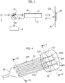
- Such an optical element 30, as exemplified in Figure 3 may be used in co-operation with a reference reflective surface 40, for instance included in the membrane layer 20 as a peripheral portion 400 surrounding a center portion 200 of its bottom surface or patterned as a non-connected reflective surface, operating as fiducial mark.
- a reference reflective surface 40 for instance co-planar with the bottom surface of the membrane 20, may facilitate performing an improved optical alignment of the focal length F of the focusing lens portion 32.
- a light beam emitted by the light source S may be concurrently focused 32 and collimated 34 when traveling through the optical element 30.
- a collimated ray of light provided therefrom may impinge onto the reflective reference surface 40.
- At least a part of the impinging collimated ray will be reflected from the reflective reference surface 40.
- a reflected ray of light R may travel backwards along the optical element 30 with the capability of being sensed, for instance via an optical circulator 31 arranged at the "distal" end of the element 30 (that is the end facing away from the reflective surface 40) .
- the circulator 31 may provide the reflected ray R to a user circuit A, for instance an actuator A, configured to perform a feedback on the alignment of the optical element 30 with respect to the reference surface 40.
- Alignment of the collimating lens 34 may thus be facilitated thanks to a bigger spot size available at the focal point FP.
- the focusing lens 32 being incorporated in a common optical assembly 30 together with the collimating lens 34 may therefore facilitate (in an essentially "passive” manner) simpler alignment for the focusing lens 32.
- the reflected light R provides a sort of passive alignment feedback, without per se activating the opto-mechanical transducer, that is without electrically powering the apparatus 10.
- the optical element 30 can be attached (e.g., glued) directly to assembly 10 once aligned therewith.
- the membrane 20 can be attached to the porthole 120 of the housing while the membrane 20 is assembled therein.
- a "target" reference surface 40, 400 as discussed herein may be located on an exposed surface portion of the optically transparent layer 16, 18 of the assembly 10, such as a surface portion aligned with the hole 120 in the housing 12 of the apparatus 10.
- planar reflective surfaces (or facets) 400A, 400B and of a corresponding pair of collimating lens portions 34A, 34B is discussed. It is otherwise understood that such quantities in exemplary arrangements are in no way limiting, as virtually any number of planar reflective surfaces (or facets) 400A, 400B and collimating lens portions 34a, 34B may be used in one or more embodiments.
- the collimating GRIN lenses 340 may be coupled to an optical spacer or "buffer", so that the total length L0 given by the sum of the length of the respective lens 340, 342 and the length of the respective spacer 342, 344 is the same for both the focusing 32 and collimating 34A, 34B portions, facilitating coupling the optical element 30 to the light source S and to the optically transparent layer 18.
- GRIN lenses 320, 340 having different pitch lengths may provide an advantageously easy assembly of the optical component 30 and may facilitate reaching the target spot size with the focal point FP at the central surface 200 of the membrane 20.
- the optical fibers embedding the focusing portion 32 and collimating portions 34A, 34B, respectively, may be assembled in a housing comprising:
- Figure 7 is an exemplary plan view of Figure 4 , showing the fiducial areas 400A, 400B, for instance two metallic square areas 400A, 400B having a side length C and whose centers are located at a same distance H from the central area 200 of the membrane 20 target for the focal point FP.
- the distance H may have a value of approximately 500 microns.
- Figure 7 also shows, represented with dashed lines superimposed on the reference reflective areas 400A, 400B and 20, spot sizes BSf, BSc output from the focusing portion 32 and collimating portion 34 of the optical element 30, respectively.
- an alignment error ⁇ c of the collimated beam BSc with respect to the reference areas 400A, 400B may be detected thanks to the signal R back-reflected from the reflective surfaces of the reference reflective areas 400A, 400B.
- Such an alignment error ⁇ c may be indicative of a corresponding alignment error ⁇ f of the focused beam with respect to the target focal point FP.
- the optical element 30 may be deemed to be aligned with respect to the reference surface 40 when the collimated beam spot size BSc fits (entirely) within the reference reflective areas 400A, 400B, that is when the alignment error ⁇ c is negligible, up to zero.
- the focal point FP can be deemed to be aligned with respect to the target position, corresponding to a negligible (ideally, up to zero) focusing alignment error ⁇ f when the collimated beam spot size BSc fits entirely within the reference reflective areas 400A, 400B, that is when the collimation alignment error ⁇ c is negligible (ideally, up to zero).
- Figure 8 is an enlarged view of the focusing portion 32 of the optical element 30, showing ray traces of a light beam propagating therethrough and output at an optical interface 330, for instance an optical window having a certain thickness T.
- the GRIN lens 320 may have a substantially cylindrical shape with a constant diameter E, e.g., between 350 and 500 microns.
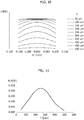
- Figure 8A is a diagram of a RMS focus beam spot size BSf, in microns, as a function of distance, in millimeters, from the ideal focal point FP taken as origin of the abscissa.
- the GRIN focusing lens 320 may have a respective length Pf about 5.35 mm
- the collimating GRIN lens 324 may have a second length Pc about 3.07 mm with the optical buffer 342 having a third length Bc about 2.28 mm, so that the total length Pc+Bc of the collimating GRIN lens and the collimating optical buffer 342 is equal to the length of focusing GRIN lens Pf.
- Figure 9A is a diagram of an RMS collimated beam spot size BSc, in microns, as a function of distance, in millimeters, from the reference surface 40 taken as origin of the abscissa.
- Figure 10 is a diagram of the amount of optical power LP reaching one of the reference surfaces 40, 400, 400A, 400B as a function of the alignment error ⁇ c calculated for various values of the length C of the reference surface.
- the total power of the light launched into the optical element 30 is considered to be equal to 1 Watt, for the sake of simplicity in performing power loss computation.
- an increased accuracy in detecting misalignments may be obtained for values of the length C of the reflective surfaces 400A, 400B in a range between 250 and 300 microns, with 250 microns the nominal best value.
- Figures 12 to 20 are illustrative of possible stages of assembling a sensor 10 along the lines discussed previously.
- such a sensor assembly 10 may comprise:
- the optical element 30 can be aligned directly with respect to the assembly 100 and coupled (e.g., glued) therewith.
- the assembly 10 may be included in a package 12 as exemplified in Figures 13, 14 having a glass window 120 and the optical element 30 can be coupled to such package window.
- the chip assembly of Figure 12 may be mounted inside the package of Figures 13 and 14 .
- Figures 13 and 14 are exemplary of a (e.g., ceramic) chip support package 12 comprising an array of electrically conductive leads 14 and a through hole 120 hosting a glass window on a bottom surface of the support 12.
- Figure 14 is a flipped perspective view of the package of Figure 13 , showing a backside 12a of the planar support 12 with the glass window 120.
- the assembly 10 may be placed and attached (e.g., glued) over the glass window 120, with a portion of the optical chip layer 18 exposed or aligned therewith.
- wire bonding may be performed to electrically couple bond pads 24 coupled to the membrane 22 and the array of leads 14 in the support 12, for electrical connection between the opto-mechanical assembly 10 and the outside of the package.
- a protective lid 90 may be attached to the package support 12, sealing the volume therein so that the chip assembly 100 is protected from external environment.
- Figure 17 shows the backside 12a of the support 12 with the membrane 20 and reference surfaces 400A, 400B visible from the optically transparent glass window 120.
- Figure 18 is a perspective view of the optical component 30 which may comprise set of three optical fibers 32, 34A, 34B, inserted inside a same optical fiber block 30 or coupled therebetween via a mechanical holder (not visible in the figure).
- Aligning the optical element 30 to the membrane 20 may comprise coupling the free output ends of the optical element 30 to the window 120 of the package 12 at the side of the window 120 exposed on the back of the package 12, as exemplified in Figure 19 .
- Figure 20 shows an enlarged view of the portion indicated by arrow XX of Figure 19 .
- a process of aligning ⁇ c, ⁇ f the optical element 30 with respect to the membrane 20 before fixedly coupling the element 30 to the window 120 may comprise:
- the focusing portion 32 is aligned by design to the working area of the membrane 20.
- An apparatus (for instance, 10) may comprise:
- An apparatus as exemplified herein may comprise a plurality of the reflective facets (400A, 400B), and in such an apparatus the optical element may incorporate: a plurality of light collimating paths (for instance, 34A, 34B) configured to provide respective light beams collimated (for instance, 340) onto the plurality of reflective facets.
- a plurality of light collimating paths for instance, 34A, 34B
- respective light beams collimated for instance, 340
- the plurality of reflective facets may comprise reflective facets arranged at a same distance (for instance, H) from a center (for instance, FP) of the piezoelectric membrane.
- the plurality of reflective facets comprises two facets arranged mirror-symmetrical from a center of the piezoelectric membrane.
- the plurality of reflective facets may comprise:
- the optical element may comprise:
- At least one of the light focusing path and of the at least one light collimating path in the optical element may include an optical spacer portion (for instance, 322, 342).
- a method as exemplified herein may comprise:
Landscapes
- Physics & Mathematics (AREA)
- General Physics & Mathematics (AREA)
- Optics & Photonics (AREA)
- Nonlinear Science (AREA)
- Optical Couplings Of Light Guides (AREA)
- Measuring Fluid Pressure (AREA)
- Investigating Or Analyzing Materials By The Use Of Ultrasonic Waves (AREA)
Abstract
an optically transparent substrate (18) having a first surface and a second surface opposed the first surface;
a piezoelectric membrane (20) arranged at the first surface of the optically transparent substrate (18), the piezoelectric membrane (20) configured to oscillate as a result of light propagated through the optically transparent substrate (18) impinging onto the piezoelectric membrane (20), wherein at least one reflective facet (40) facing the optically transparent substrate (18) is provided at the piezoelectric membrane (20) ;
an optical element (30) configured to receive a light beam at an input end and to guide the light beam towards an output end couplable to the second surface of the optically transparent substrate (18),
Description
- The description relates to opto-mechanical systems.
- One or more embodiments may be used for optical alignment.
- Micro-opto-electromechanical systems (briefly, MOEMS), also known as optical (micro)electromechanical systems or optical MEMS, are systems involving sensing or manipulating optical signals, on a very small size scale, using integrated mechanical, optical, and electrical systems, coupling a mechanical mode to a light mode and vice versa, for instance.
- Such a type of systems is discussed, for instance, in Midolo, L., Schliesser, A. and Fiore, A.: "Nano-opto-electro-mechanical systems", Nature Nanotech 13, 11-18 (2018), doi: 10.1038/s41565-017-0039-1
- An opto-mechanical sensor may transduce mechanical movement of a membrane (on a micrometer scale) into an optical signal and vice versa.
- For instance, an opto-mechanical sensor may comprise an oscillating (nano-/micro-)membrane with a light beam focused on an active area of the membrane, that is the area where the opto-mechanical transduction may be maximum. Such an active area may be arranged, for instance, at the center of the die, or at any other portion thereof.
- Such a type of sensor is disclosed, for instance, in A. Simonsen, S. Saarinen, J. Sanchez, J. Ardenkjær-Larsen, A. Schliesser, and E. Polzik: "Sensitive optomechanical transduction of electric and magnetic signals to the optical domain," Opt. Express 27, 18561-18578 (2019).
- In membrane-based opto-mechanical sensors of this type, the light beam used is focused up to reaching a target spot size, e.g., of the order of micrometers.
- As a result, optical alignment between (a focal point of) the focused light beam and the (active) area of the membrane is a relevant figure of merit.
- Optical alignment using a focused beam may be challenging for various reasons, such as:
- a difficulty in precisely determining a correct position for the minimum waist point of the light beam, which may result in poor performance and a difficulty in optimizing alignment;
- complexity of the search algorithms for a best alignment.
- Conventional optical alignment arrangements using a focused beam may involve a complex reading process including:
- performing a scan along X and Y axes for each position along the optical propagation direction (usually referred to as the Z axis);
- analyzing all the data in order to find a correct focusing depth;
- setting the system to a certain focusing depth;
- performing a further scan for determining an improved alignment.
- Conventional solutions as discussed in the foregoing thus suffer from the following drawbacks:
- complexity of alignment systems and methods;
- costs in terms of time and consumption, as related to direct reading and feedback from the opto-electronic device/component.
- An object of one or more embodiments is to contribute in overcoming the drawbacks discussed in the foregoing.
- According to one or more embodiments, such an object can be achieved by means of an electro-optical apparatus having the features set forth in the claims that follow.
- One or more embodiments may relate to a corresponding optical alignment method.
- The claims are an integral part of the technical teaching provided herein with reference to the embodiments.
- One or more embodiments may comprise an optical element. A gradient-index, briefly GRIN, optical lens may be exemplary of such a lens.
- One or more embodiments may offer one or more of the following advantages:
- use of a GRIN lens directly attached to a surface counters possible focusing misalignment errors;
- direct reading of the chip performances may become superfluous;
- optical alignment can be performed with standard equipment and procedures;
- using reflected power of a collimated light beam for performing optical alignment may render reading chip performance superfluous, which simplifies the alignment process.
- One or more embodiments may involve combining a GRIN lens with an optical buffer, so that the total length of the focusing and collimating system is the same.
- One or more embodiments may involve reading the reflected power of a collimated beam, which facilitates "skipping" direct reading of the chip.
- In one or more embodiments, advantageously, a focusing system and a collimating system may be placed in a same optical fiber block, so that the stability in relative positional arrangements is a function of the accuracy in the assembly of a single fiber block (approximately 1 micron).
- In one or more embodiments, reflective geometries can be patterned on the chip, which facilitates providing optical fiducial marks, for instance.
- One or more embodiments will now be described, by way of non-limiting example only, with reference to the annexed Figures, wherein:
-
Figure 1 is a cross-sectional view of an opto-mechanical transducer assembly, -
Figures 2, 2A and 2B are diagrams of principles underlying one or more embodiments; -
Figure 3 is a diagram of an optical alignment method as exemplified herein; -
Figure 4 is a perspective view of an alignment system as per the present disclosure; -
Figure 5 is a cross-sectional view along line V-V ofFigure 4 ; -
Figure 6 is a cross-sectional view along line VI-VI ofFigure 4 ; -
Figure 7 is a plan view ofFigure 4 ; -
Figures 8, 8A, 9 and 9A are diagrams of optical principles underlying one or more embodiments; -
Figures 10 and 11 are diagrams of power distribution; -
Figure 12 is a perspective view of an assembly as exemplified herein; -
Figures 13 and 14 are perspective views of a housing as per the present disclosure; -
Figures 15, 16 and17 are perspective views of an opto-mechanical assembly as per the present disclosure; -
Figure 18 is a perspective view of an optical element as per the present disclosure; -
Figure 19 is a perspective view of an apparatus as per the present disclosure; -
Figure 20 is an enlarged view essentially along arrow XX ofFigure 19 . - In the ensuing description, one or more specific details are illustrated, aimed at providing an in-depth understanding of examples of embodiments of this description. The embodiments may be obtained without one or more of the specific details, or with other methods, components, materials, etc. In other cases, known structures, materials, or operations are not illustrated or described in detail so that certain aspects of embodiments will not be obscured.
- Reference to "an embodiment" or "one embodiment" in the framework of the present description is intended to indicate that a particular configuration, structure, or characteristic described in relation to the embodiment is comprised in at least one embodiment. Hence, phrases such as "in an embodiment" or "in one embodiment" that may be present in one or more points of the present description do not necessarily refer to one and the same embodiment.
- Moreover, particular conformations, structures, or characteristics may be combined in any adequate way in one or more embodiments.
- The headings/references used herein are provided merely for convenience and hence do not define the extent of protection or the scope of the embodiments.
- For the ease of explanation, the drawings are in simplified form and are not to a precise scale.
- Throughout the figures annexed herein, like parts or elements are indicated with like references symbols and a corresponding description will not be repeated for each and every figure for brevity.
- An opto-
mechanical transducer 10 as exemplified inFigure 1 may comprise: - a
housing 12, for instance a ceramic housing, comprising a base with acentral hole 120, for instance, with a diameter about 4 mm (1mm= 10-3m = 1 millimeter) and configured as a porthole to hold an optically transparent material, for instance made of glass having a thickness of 0.2 mm, forming an optical window; - a plurality of electrically conductive leads 14, for instance flat leads exposed at the surface of the
housing 12; - one or more optically
transparent layers core 160 extending, for instance, about a thickness of 0.35 mm; - a
membrane layer 20, for instance a piezoelectric membrane, located on a top planar surface of the silica die 18 and comprising an at least partially reflective "bottom"surface 200 facing towards the top planar surface of the silica die 18; - (micro-)
spacers 22 configured to hold themembrane layer 20 separate from the top planar surface of the silica die 18 so as to allow the membrane to vibrate or oscillate; - electrically
conductive contact pads 24 coupled on a top surface of themembrane layer 20 and configured to control and/or detect variations of opto-mechanical properties of themembrane 20 via electrical signals transmitted therefrom or received thereto; - electrically
conductive wires 26 coupling the electricallyconductive contact pads 24 on themembrane layer 20 to electrically conductive leads 14 in thesupport base 12; - an
optical element 30 such as a lens, configured to guide light emitted from a source at an input end (not visible in the figure) of theoptical element 30 along an optical path aimed towards themembrane 20, theoptical element 30 is coupled to thepackage base 12 via theporthole 120 therein. For instance, the optical element may have a diameter about 2.5 mm and a length about the same size. - As exemplified in
Figure 1 , theapparatus 10 may be (hermetically) sealed via acasing 90, such as a lid, for instance. - In one or more embodiments, the opto-
mechanical apparatus 10 may transduce an optical signal to an electric signal via mechanical vibration of themembrane layer 20 when light is focused thereon. - A GRIN lens as illustrated in
Figure 2 is exemplary of anoptical element 30 which can be advantageously used in embodiments as discussed herein. - By way of background, it may be recalled that an "optical object" 30A as shown in
Figure 2A , configured to focus a light beam with parallel rays from a light source S, "squeezing" it to a focal point FP at a certain focal depth or distance F from theobject 30, is referred to as a focusinglens 30A. A corresponding position along a propagation axis Z wherein the light beam spot reaches its minimum radius is called "focal point" FP (or beam waist). - Conversely, an optical object 30B as shown in
Figure 2B , which receives a diverging beam from a source S and generates a beam with no angular divergence left (in a notionally ideal scenario) or with a Gaussian behavior (in a more realistic scenario), is referred as a collimating lens 30B. A collimating lens 30B may have a collimating length, that is distance between the source S and the lens 30B such that the beam from the light source is collimated. - A
GRIN lens 30 as exemplified inFigure 2 may comprises a cylindrical or rod-like body, extending linearly (that is, longitudinally) between twoflat ends - The optical behavior of a
GRIN lens 30 may be based on the refractive index of the lens material, which varies spatially with a gradient profile, in ways per se known to those of skill in the art. -
Figure 2 shows a diagram of ray traces within aGRIN rod 30 designed to operate as a focusing lens. The linear rod-like body 30 may have a length, also indicated as one "pitch" P, that is the length for obtaining a 1:1 image without reversing which is related to the refractive index variation of each GRIN lens. - As known to those of skill in the art, a GRIN lens may behave as a focusing lens or a collimating lens (or as a diverging lens) as a function of its pitch P.
- For instance, shortening the rod to a fractional length of ½ or ¼ of the full pitch P, as exemplified in
Figure 2 with inverted arrows, may vary the optical properties of theoptical element 30. - In an
apparatus 10 as exemplified inFigure 1 , a GRIN lens may be used at 30 in order to focus a light beam (as exemplified inFigure 2A ) on themembrane bottom surface 200. - On the other hand, as discussed previously, accurately aligning a focused light beam so that its waist is at a position corresponding to the
bottom surface 200 may be a challenging task. - As exemplified in
Figure 3 , one or more embodiments may use anoptical element 30 based on the GRIN lens concept which includes a focusinglens portion 32 and acollimating lens portion 34 embedded in a single optical piece, for instance in a single (light) fiber block. - Such an
optical element 30 may be designed so that both the focusinglens portion 32 and thecollimating lens portion 34 have respective (focal) lengths F correlated therebetween, for instance thanks to being formed together in a single fiber block with a certain length. - Such an
optical element 30, as exemplified inFigure 3 , may be used in co-operation with a referencereflective surface 40, for instance included in themembrane layer 20 as aperipheral portion 400 surrounding acenter portion 200 of its bottom surface or patterned as a non-connected reflective surface, operating as fiducial mark. Such a referencereflective surface 40, for instance co-planar with the bottom surface of themembrane 20, may facilitate performing an improved optical alignment of the focal length F of the focusinglens portion 32. - For instance, a light beam emitted by the light source S may be concurrently focused 32 and collimated 34 when traveling through the
optical element 30. As a result, a collimated ray of light provided therefrom may impinge onto thereflective reference surface 40. - At least a part of the impinging collimated ray will be reflected from the
reflective reference surface 40. Such a reflected ray of light R may travel backwards along theoptical element 30 with the capability of being sensed, for instance via anoptical circulator 31 arranged at the "distal" end of the element 30 (that is the end facing away from the reflective surface 40) . For instance, thecirculator 31 may provide the reflected ray R to a user circuit A, for instance an actuator A, configured to perform a feedback on the alignment of theoptical element 30 with respect to thereference surface 40. - Alignment of the collimating
lens 34 may thus be facilitated thanks to a bigger spot size available at the focal point FP. - The focusing
lens 32 being incorporated in a commonoptical assembly 30 together with the collimatinglens 34 may therefore facilitate (in an essentially "passive" manner) simpler alignment for the focusinglens 32. - It is noted that the reflected light R provides a sort of passive alignment feedback, without per se activating the opto-mechanical transducer, that is without electrically powering the
apparatus 10. - As mentioned, such a passive alignment process is relatively quick and easy.
- For instance, the
optical element 30 can be attached (e.g., glued) directly toassembly 10 once aligned therewith. - Alternatively, it can be attached to the
porthole 120 of the housing while themembrane 20 is assembled therein. - In an
optical alignment system Figures 4 to 7 , for instance: - the
reference surface 40 may comprise a plurality of planar reflective surfaces (or facets) 400A, 400B which may be symmetrically arranged with respect to themembrane layer 20, at a same distance from a target focal point FP of theactive surface 200 of themembrane 20; and - the
optical element 30 may comprise a plurality of collimatinglens portions lens portion 32 of theoptical element 30. - A "target"
reference surface transparent layer assembly 10, such as a surface portion aligned with thehole 120 in thehousing 12 of theapparatus 10. - For the sake of simplicity, in the following an arrangement of a pair of planar reflective surfaces (or facets) 400A, 400B and of a corresponding pair of collimating
lens portions collimating lens portions 34a, 34B may be used in one or more embodiments. - As exemplified in
Figure 5 (this is a cross-sectional view along line V-V ofFigure 4 ): - the focusing
lens portion 32 of theoptical element 30 may be incorporated in an optical fiber comprising a focusingGRIN lens portion 320 and anoptical spacer portion 322; - the pair of collimating
lens portions collimating lens portion 34A and a second collimating lens portion 24B, each comprising a collimatingGRIN lens portion 340 and a furtheroptical spacer portion 342. - For a certain light wavelength, a focusing
GRIN lens 320 may be obtained for a certain pitch P, e.g., P=500 microns, while acollimating GRIN lens 340 may be obtained for a fraction of the pitch, e.g., P'=1/2*P. - As the
collimating lenses 340 are shorter than the focusinglens 320, thecollimating GRIN lenses 340 may be coupled to an optical spacer or "buffer", so that the total length L0 given by the sum of the length of therespective lens respective spacer 342, 344 is the same for both the focusing 32 and collimating 34A, 34B portions, facilitating coupling theoptical element 30 to the light source S and to the opticallytransparent layer 18. - Use of
GRIN lenses optical component 30 and may facilitate reaching the target spot size with the focal point FP at thecentral surface 200 of themembrane 20. - As exemplified in
Figure 6 (this is a cross-sectional view along line VI-VI ofFigure 4 ), the optical fibers embedding the focusingportion 32 andcollimating portions - a
support layer 60 comprising a number of V-grooves 600 wherein thefibers - a
lid layer 64, configured to be arranged on thefibers grooves 600, - a
filling layer 62, for instance a layer of an epoxy resin, sandwiched between thesupport layer 60 and thelid layer 64, and filling the interstitial spaces between the V-grooves 600, thefibers lid layer 64. -
Figure 7 is an exemplary plan view ofFigure 4 , showing thefiducial areas square areas central area 200 of themembrane 20 target for the focal point FP. - For instance, the distance H may have a value of approximately 500 microns.
-
Figure 7 also shows, represented with dashed lines superimposed on the referencereflective areas portion 32 and collimatingportion 34 of theoptical element 30, respectively. - For instance, as exemplified in
Figure 7 : - the focused beam spot size BSf may reach a waist size below 20 µm, ideally 10 µm (1 µm = 10-6 m = 1 micron);
- the collimated beams spot sizes BSc may be about 300 µm at the respective
fiducial area - During optical alignment operations, an alignment error δc of the collimated beam BSc with respect to the
reference areas reflective areas - In one or more embodiments, the
optical element 30 may be deemed to be aligned with respect to thereference surface 40 when the collimated beam spot size BSc fits (entirely) within the referencereflective areas reflective areas -
Figure 8 is an enlarged view of the focusingportion 32 of theoptical element 30, showing ray traces of a light beam propagating therethrough and output at anoptical interface 330, for instance an optical window having a certain thickness T. - As exemplified in
Figure 8 , the focusingportion 32 may have a total length L0 given by the sum of a length Pf of the focusingGRIN lens 320, for instance equal to a full pitch and about 500 micron, and a length Bf of the focusingbuffer 322, for instance made of fused silica, e.g. L0=Pf+Bf. - For instance, the
GRIN lens 320 may have a substantially cylindrical shape with a constant diameter E, e.g., between 350 and 500 microns. -
Figure 8A is a diagram of a RMS focus beam spot size BSf, in microns, as a function of distance, in millimeters, from the ideal focal point FP taken as origin of the abscissa. - As exemplified in
Figure 9 , the collimatingportion 34 may have a total length L0 given by the sum of a length Pc of thecollimating GRIN lens 340, for instance about half of a lens pitch, and a length Bc of thecollimating buffer 342, for instance made of fused silica, e.g., L0=Pc+Bc. - In one or more embodiments, such a total length L0 is the same for the focusing
portion 32 and for the collimatingportion 34, e.g., L0=Pc+Bc=Pf+Bf. - For instance, the
GRIN focusing lens 320 may have a respective length Pf about 5.35 mm, the collimating GRIN lens 324 may have a second length Pc about 3.07 mm with theoptical buffer 342 having a third length Bc about 2.28 mm, so that the total length Pc+Bc of the collimating GRIN lens and the collimatingoptical buffer 342 is equal to the length of focusing GRIN lens Pf. -
Figure 9A is a diagram of an RMS collimated beam spot size BSc, in microns, as a function of distance, in millimeters, from thereference surface 40 taken as origin of the abscissa. -
Figure 10 is a diagram of the amount of optical power LP reaching one of the reference surfaces 40, 400, 400A, 400B as a function of the alignment error δc calculated for various values of the length C of the reference surface. In the example considered, the total power of the light launched into theoptical element 30 is considered to be equal to 1 Watt, for the sake of simplicity in performing power loss computation. -
Figure 11 is a diagram of the difference ΔLP between values of power at zero misalignment, e.g., δc=0, and power values with a maximum misalignment, e.g., δc=0.1 micron, plotted as a function of the corresponding reflective surface length C. - As exemplified in
Figures 10 and 11 , an increased accuracy in detecting misalignments may be obtained for values of the length C of thereflective surfaces -
Figures 12 to 20 are illustrative of possible stages of assembling asensor 10 along the lines discussed previously. - As illustrated in particular in
Figure 12 , such asensor assembly 10 may comprise: - an
optical chip layer 18, e.g., an optically transparent fused silica layer; - an
active membrane 20, such as a nano membrane of piezoelectric material, for instance; - a pair of electrically
conductive bonding pads 24 coupled to the membrane, where the working area of themembrane 20 is placed betweenbonding pads 24 which are configured to be used for providing electrical connection between leads and themembrane 20; - a pair of
reference surfaces membrane 20 so that their position with respect tomembrane 20 is well defined, which may comprise metallic or other reflective coating provided in the chip by lithography, in a way per se known. - In one or more embodiments, the
optical element 30 can be aligned directly with respect to theassembly 100 and coupled (e.g., glued) therewith. - Alternatively, the
assembly 10 may be included in apackage 12 as exemplified inFigures 13, 14 having aglass window 120 and theoptical element 30 can be coupled to such package window. For instance, the chip assembly ofFigure 12 may be mounted inside the package ofFigures 13 and 14 . -
Figures 13 and 14 are exemplary of a (e.g., ceramic)chip support package 12 comprising an array of electrically conductive leads 14 and a throughhole 120 hosting a glass window on a bottom surface of thesupport 12.Figure 14 is a flipped perspective view of the package ofFigure 13 , showing abackside 12a of theplanar support 12 with theglass window 120. - As exemplified in
Figure 15 , theassembly 10 may be placed and attached (e.g., glued) over theglass window 120, with a portion of theoptical chip layer 18 exposed or aligned therewith. As exemplified inFigures 15 and17 , wire bonding may be performed to electrically couplebond pads 24 coupled to themembrane 22 and the array ofleads 14 in thesupport 12, for electrical connection between the opto-mechanical assembly 10 and the outside of the package. - In one or more embodiments as exemplified in
Figure 16 , aprotective lid 90 may be attached to thepackage support 12, sealing the volume therein so that thechip assembly 100 is protected from external environment. -
Figure 17 shows thebackside 12a of thesupport 12 with themembrane 20 andreference surfaces transparent glass window 120. -
Figure 18 is a perspective view of theoptical component 30 which may comprise set of threeoptical fibers optical fiber block 30 or coupled therebetween via a mechanical holder (not visible in the figure). - Aligning the
optical element 30 to themembrane 20 may comprise coupling the free output ends of theoptical element 30 to thewindow 120 of thepackage 12 at the side of thewindow 120 exposed on the back of thepackage 12, as exemplified inFigure 19 . -
Figure 20 shows an enlarged view of the portion indicated by arrow XX ofFigure 19 . - In an arrangement as illustrated herein, a process of aligning δc, δf the
optical element 30 with respect to themembrane 20 before fixedly coupling theelement 30 to thewindow 120 may comprise: - transmitting S a pair of collimating light beams BSc towards the reflecting reference surfaces 400A, 400B while transmitting a focusing light beam BSf towards the
membrane 20; - receiving 31 a back-reflected light signal R from the
reflective surfaces - varying, for instance via actuators A, a position of the
optical element 30 with respect to the glass window 120 (and to the membrane 20) as a function of the back-reflected signal R. - As a result, it is possible align δc, δf the
collimating lenses - Since the position of the reference
reflective surfaces membrane 20 and since theoptical fibers portion 32 is aligned by design to the working area of themembrane 20. - An apparatus (for instance, 10) may comprise:
- an optically transparent substrate (for instance, 18) having a first surface and a second surface opposed the first surface;
- a piezoelectric membrane (for instance, 20) arranged at the first surface of the optically transparent substrate, the piezoelectric membrane configured to oscillate as a result of light propagated through the optically transparent substrate impinging onto the piezoelectric membrane, wherein at least one reflective facet (for instance, 40, 400A, 400B) facing the optically transparent substrate is provided at the piezoelectric membrane;
- an optical element (for instance, 30) configured to receive a light beam at an input end and to guide the light beam towards an output end couplable to the second surface of the optically transparent substrate;
- wherein the optical element incorporates:
- a light focusing path (for instance, 32) configured to focus (for instance, 320) a light beam at a focal point (for instance, FP) at the piezoelectric membrane, and
- at least one light collimating path (for instance, 34, 34A, 34B) configured to collimate (for instance, 340) the light beam onto the at least one reflective facet;
- wherein the optical element is configured to guide light reflected (for instance, R, 31) from the at least one reflective facet to the input end,
- wherein the light reflected to the input end is indicative of the position (for instance, δc, δf) of the optical element with respect to the focal point.
- In an apparatus as exemplified herein:
- the piezoelectric membrane may comprise the at least one reflective facet (for instance, 40), the at least one reflective facet having a central area (for instance, 200) and a peripheral area (for instance, 400), and
- the light focusing path in the optical element is configured to focus the light beam at the central area (for instance, 200, FP) of the at least one reflective facet, and
- the at least one light collimating path in the optical element is configured to collimate (for instance, 340) the light beam at the peripheral area of the at least one reflective facet.
- An apparatus as exemplified herein may comprise a plurality of the reflective facets (400A, 400B), and in such an apparatus the optical element may incorporate:
a plurality of light collimating paths (for instance, 34A, 34B) configured to provide respective light beams collimated (for instance, 340) onto the plurality of reflective facets. - In an apparatus as exemplified herein, the plurality of reflective facets may comprise reflective facets arranged at a same distance (for instance, H) from a center (for instance, FP) of the piezoelectric membrane.
- In an apparatus as exemplified herein, the plurality of reflective facets comprises two facets arranged mirror-symmetrical from a center of the piezoelectric membrane.
- In an apparatus as exemplified herein, the plurality of reflective facets may comprise:
- square facets with a side length (for instance, C) between about 250 and about 300 microns, and/or
- facets at a distance (for instance, H) of about 300 microns from a center of the piezoelectric membrane.
- In an apparatus as exemplified herein, the optical element may comprise:
- a substrate (for instance, 60) having a plurality of channels (for instance, 600) formed therein,
- a plurality of optical fibers (for instance, 32, 34, 34A, 34B) arranged in the channels (for instance, 600), and
- the optical fibers (for instance, 32, 34, 34A, 34B) providing the light focusing path (for instance, 32) and the at least one light collimating path (for instance, 34, 34A, 34B).
- In an apparatus as exemplified herein:
- the light focusing path in the optical element may comprise a light focusing gradient index, GRIN, lens (for instance, 320) with a focusing pitch (for instance, Pf),
- the at least one light collimating path in the optical element comprises a light collimating GRIN lens (for instance, 34A, 34B) having a collimating pitch (for instance, Pc), and the light focusing and light collimating paths may have a same total length (for instance, L0) and a same lens diameter (for instance, E) .
- In an apparatus as exemplified herein, at least one of the light focusing path and of the at least one light collimating path in the optical element may include an optical spacer portion (for instance, 322, 342).
- In an apparatus as exemplified herein:
- the same total length may be about 500 microns, and/or
- the same lens diameter may be about 350 microns.
- In an apparatus as exemplified herein:
- the apparatus may comprise a housing (for instance, 12, 90) having a support base (for instance, 12) with a through hole (for instance, 120) therein, the support base of the housing being coupled to the second surface of the optically transparent substrate with a portion of the second surface of the optically transparent substrate aligned with the through hole; and
- the output end of the optical element is coupled to the optically transparent layer at the through hole in the support base of the housing.
- A method as exemplified herein may comprise:
- launching (for instance, S) into the input end of the optical element (for instance, 30) of an opto-mechanical apparatus (for instance, 10) as exemplified herein, a light beam aimed at the at least one reflective facet (for instance, 40, 400A, 400B);
- sensing (for instance, 31) light (for instance, R) reflected towards the input end of the optical element (for instance, 30); and
- aligning (for instance, A) the optical element with respect to the focal point (for instance, FP) at the piezoelectric membrane (for instance, 20) of the apparatus (10) as a function of the reflected light sensed.
- It will be otherwise understood that the various individual implementing options exemplified throughout the figures accompanying this description are not necessarily intended to be adopted in the same combinations exemplified in the figures. One or more embodiments may thus adopt these (otherwise non-mandatory) options individually and/or in different combinations with respect to the combination exemplified in the accompanying figures.
- Without prejudice to the underlying principles, the details and embodiments may vary, even significantly, with respect to what has been described by way of example only, without departing from the extent of protection. The extent of protection is defined by the annexed claims.
Claims (18)
- An apparatus (10), comprising:an optically transparent substrate (18) having a first surface and a second surface opposed said first surface;a piezoelectric membrane (20) arranged at the first surface of the optically transparent substrate (18), the piezoelectric membrane (20) configured to oscillate as a result of light propagated through the optically transparent substrate (18) impinging onto the piezoelectric membrane (20), wherein at least one reflective facet (40, 400A, 400B) facing the optically transparent substrate (18) is provided at the piezoelectric membrane (20);an optical element (30) configured to receive a light beam at an input end and to guide said light beam towards an output end couplable to said second surface of said optically transparent substrate (18);wherein said optical element (30) incorporates:a light focusing path (32) configured to focus (320) a light beam at a focal point (FP) at said piezoelectric membrane (20), andat least one light collimating path (34, 34A, 34B) configured to collimate (340) said light beam onto said at least one reflective facet (40, 400A, 400B);wherein said optical element (30) is configured to guide light reflected (R, 31) from said at least one reflective facet (40, 400A, 400B) to said input end,wherein the light reflected (R, 31) to said input end is indicative of the position (δc, δf) of said optical element (30) with respect to said focal point (FP) .
- The apparatus (10) of claim 1, wherein:the piezoelectric membrane (20) comprises said at least one reflective facet (40), said at least one reflective facet (40) having a central area (200) and a peripheral area (400), andsaid light focusing path (32) in said optical element (30) is configured to focus (320) said light beam at said central area (200, FP) of said at least one reflective facet (40), andsaid at least one light collimating path (34) in said optical element (30) is configured to collimate (340) said light beam at said peripheral area (400) of said at least one reflective facet (40).
- The apparatus (10) of claim 1, comprising:
a plurality of said reflective facets (400A, 400B), and wherein said optical element (30) incorporates:
a plurality of light collimating paths (34A, 34B) configured to provide respective light beams collimated (340) onto said plurality of reflective facets (400A, 400B) . - The apparatus (10) of claim 3, wherein the plurality of reflective facets (400A, 400B) comprises reflective facets arranged at a same distance (H) from a center (FP) of the piezoelectric membrane (20).
- The apparatus (10) of claim 3 or 4, wherein said plurality of reflective facets (400A, 400B) comprises two facets arranged mirror-symmetrical from a center (FP) of the piezoelectric membrane (20).
- The apparatus (10) of claim 4 or claim 5, wherein said plurality of reflective facets (400A, 400B) comprises:square facets with a side length (C) between about 250 and about 300 microns, and/orfacets at a distance (H) of about 300 microns from a center (FP) of the piezoelectric membrane (20).
- The apparatus (10) of any of the previous claims, wherein said optical element (30) comprises:a substrate (60) having a plurality of channels (600) formed therein,a plurality of optical fibers (32, 34, 34A, 34B) arranged in said channels (600), andthe optical fibers (32, 34, 34A, 34B) providing said light focusing path (32) and said at least one light collimating path (34, 34A, 34B).
- The apparatus (10) of any of the previous claims, wherein:said light focusing path (32) in said optical element (30) comprises a light focusing gradient index, GRIN, lens (320) with a focusing pitch (Pf),said at least one light collimating path (34, 34A, 34B) in said optical element (30) comprises a light collimating GRIN lens (34A, 34B) having a collimating pitch (Pc), and said light focusing and light collimating paths (32, 34, 34A, 34B) have a same total length (Lo) and a same lens diameter (E).
- The apparatus (10) of claim 8, wherein at least one of said light focusing path (32) and of said at least one light collimating path (34, 34A, 34B) in said optical element (30) includes an optical spacer portion (322, 342) .
- The apparatus (10) of claim 8 or claim 9, wherein:said same total length (L0) is about 500 microns, and/orsaid same lens diameter (E) is about 350 microns.
- The apparatus (10) of any of the previous claims, wherein:the apparatus comprises a housing (12, 90) having a support base (12) with a through hole (120) therein, said support base (12) of said housing (12, 90) being coupled to said second surface of said optically transparent substrate (18) with a portion of said second surface of the optically transparent substrate (18) aligned with said through hole (120); andsaid output end of said optical element (30) is coupled to said optically transparent layer (18) at said through hole (120) in said support base (12) of said housing (12, 90).
- A method, comprising:launching (S) into said input end of said optical element (30) of an opto-mechanical apparatus (10) according to any of the previous claims, a light beam aimed at said at least one reflective facet (40, 400A, 400B);sensing (31) light (R) reflected to said input end of said optical element (30); andaligning (A) said optical element (30) with respect to said focal point (FP) at said piezoelectric membrane (20) of said apparatus (10) as a function of said reflected light (R) sensed (31).
- An apparatus (10), comprising:an optically transparent substrate (18) comprising:a first surface; anda second surface opposite the first surface;a piezoelectric membrane (20) disposed at the first surface of the optically transparent substrate (18);at least one reflective facet (40, 400A, 400B) disposed at the piezoelectric membrane (20) or in a same plane by a side of the piezoelectric membrane (20), and facing the optically transparent substrate (18); andan optical element (30) comprising:an input end configured to receive a light beam;an output end coupled to the second surface of the optically transparent substrate (18);a light focusing lens (32) having a focal point (FP) for the light beam at the piezoelectric membrane (20); anda light collimating lens (24) oriented to collimate the light beam onto the at least one reflective facet (40, 400A, 400B) for reflection back to the input end.
- The apparatus (10) of claim 13, wherein:the piezoelectric membrane (20) comprises the at least one reflective facet (40, 400A, 400B), the at least one reflective facet (40, 400A, 400B) having a central area and a peripheral area;the light focusing (32) has the focal point (FP) for the light beam at the central area of the at least one reflective facet (40, 400A, 400B); andthe light collimating lens is oriented to collimate the light beam at the peripheral area of the at least one reflective facet.
- The apparatus (10) of claim 13, further comprising a plurality of the reflective facets (400A, 400B), wherein the optical element (30) incorporates a plurality of light collimating lenses (34A, 34B) oriented to collimate respective light beams onto the plurality of the reflective facets (400A, 400B).
- The apparatus (10) of claim 13, wherein the optical element (30) comprises:a substrate (60) having a plurality of channels (600) formed therein; anda plurality of optical fibers (32, 34, 34A, 34B) arranged in the channels (600);wherein the optical fibers (32, 34, 34A, 34B) provide a light focusing path (320, 322) for the light focusing lens (32) and a light collimating path (340, 342) for the light collimating lens (34).
- The apparatus of claim 13, wherein:the light focusing lens (32) is a light focusing gradient index, GRIN, lens (320) with a focusing pitch (Pf); andthe light collimating lens (34) is a light collimating GRIN lens (340) having a collimating pitch (Pc), and wherein the light focusing lens (320) and the light collimating lens (340) have a same lens diameter (E) .
- The apparatus (10) of claim 13, wherein:the apparatus (10) further comprises a housing (12, 90) having a support base (12) with a through hole (120) therein, the support base (12) of the housing (12, 90) being coupled to the second surface of the optically transparent substrate (18) with a portion of the second surface of the optically transparent substrate (18) aligned with the through hole (120); andthe output end of the optical element (30) is coupled to the optically transparent substrate (18) at the through hole (120) in the support base (12) of the housing (12, 90).
Applications Claiming Priority (1)
| Application Number | Priority Date | Filing Date | Title |
|---|---|---|---|
| IT102020000013462A IT202000013462A1 (en) | 2020-06-05 | 2020-06-05 | OPTO-MECHANICAL TRANSDUCER APPARATUS AND CORRESPONDING PROCEDURE |
Publications (2)
| Publication Number | Publication Date |
|---|---|
| EP3919945A1 true EP3919945A1 (en) | 2021-12-08 |
| EP3919945B1 EP3919945B1 (en) | 2024-06-26 |
Family
ID=72087094
Family Applications (1)
| Application Number | Title | Priority Date | Filing Date |
|---|---|---|---|
| EP21176460.0A Active EP3919945B1 (en) | 2020-06-05 | 2021-05-28 | An opto-mechanical transducer apparatus and corresponding method |
Country Status (3)
| Country | Link |
|---|---|
| US (1) | US11598920B2 (en) |
| EP (1) | EP3919945B1 (en) |
| IT (1) | IT202000013462A1 (en) |
Citations (1)
| Publication number | Priority date | Publication date | Assignee | Title |
|---|---|---|---|---|
| CN110488340A (en) * | 2019-07-29 | 2019-11-22 | 中国科学院西安光学精密机械研究所 | An ultra-small interferometric ultrafast X-ray optical fiber detector |
Family Cites Families (2)
| Publication number | Priority date | Publication date | Assignee | Title |
|---|---|---|---|---|
| US4991150A (en) * | 1989-08-10 | 1991-02-05 | Wixom Michael R | Electroluminescent optical fiber shock sensor |
| EP0419021A3 (en) * | 1989-08-30 | 1991-10-09 | Schlumberger Industries Limited | Sensors with vibrating elements |
-
2020
- 2020-06-05 IT IT102020000013462A patent/IT202000013462A1/en unknown
-
2021
- 2021-05-21 US US17/326,955 patent/US11598920B2/en active Active
- 2021-05-28 EP EP21176460.0A patent/EP3919945B1/en active Active
Patent Citations (1)
| Publication number | Priority date | Publication date | Assignee | Title |
|---|---|---|---|---|
| CN110488340A (en) * | 2019-07-29 | 2019-11-22 | 中国科学院西安光学精密机械研究所 | An ultra-small interferometric ultrafast X-ray optical fiber detector |
Non-Patent Citations (5)
| Title |
|---|
| A. SIMONSENS. SAARINENJ. SANCHEZJ. ARDENKJ R-LARSENA. SCHLIESSERE. POLZIK: "Sensitive optomechanical transduction of electric and magnetic signals to the optical domain", OPT. EXPRESS, vol. 27, 2019, pages 18561 - 18578 |
| MARTIN VAN BUREN ET AL: "Foundations for low-loss fiber gradient-index lens pair coupling with the self-imaging mechanism", APPLIED OPTICS, vol. 42, no. 3, 20 January 2003 (2003-01-20), US, pages 550, XP055486666, ISSN: 0003-6935, DOI: 10.1364/AO.42.000550 * |
| MIDOLO, L.SCHLIESSER, A.FIORE, A.: "Nano-opto-electro-mechanical systems", NATURE NANOTECH, vol. 13, 2018, pages 11 - 18, XP036429618, DOI: 10.1038/s41565-017-0039-1 |
| R. W. ANDREWS ET AL: "Bidirectional and efficient conversion between microwave and optical light", NATURE PHYSICS, vol. 10, no. 4, 1 April 2014 (2014-04-01), GB, pages 321 - 326, XP055600106, ISSN: 1745-2473, DOI: 10.1038/nphys2911 * |
| T. BAGCI ET AL: "Optical detection of radio waves through a nanomechanical transducer", NATURE, vol. 507, no. 7490, 5 March 2014 (2014-03-05), pages 81 - 85, XP055173694, ISSN: 0028-0836, DOI: 10.1038/nature13029 * |
Also Published As
| Publication number | Publication date |
|---|---|
| US20210382332A1 (en) | 2021-12-09 |
| US11598920B2 (en) | 2023-03-07 |
| IT202000013462A1 (en) | 2021-12-05 |
| EP3919945B1 (en) | 2024-06-26 |
Similar Documents
| Publication | Publication Date | Title |
|---|---|---|
| US6717733B2 (en) | Collimator array | |
| JP4414650B2 (en) | Beam steering device and optical switch | |
| CN104364689A (en) | Coupling device with structured reflective surface for coupling fiber input/output | |
| CA2387538A1 (en) | Optical subassembly | |
| US6280100B1 (en) | Fiber optic connector with micro-alignable sensing fiber and associated fabrication method | |
| CN113227861A (en) | Multi-channel mode converter with silicon lens | |
| US10175425B2 (en) | Integrated polarizing and analyzing optical fiber collimator device and methods of use thereof | |
| CN215905853U (en) | Optical-mechanical device | |
| JP2004279618A (en) | Optical collimator structure | |
| US11598920B2 (en) | Opto-mechanical transducer apparatus and corresponding method | |
| US6877911B2 (en) | Optical-fiber supporting member and optical transmission device using the same | |
| JP2013221807A (en) | Optical fiber strain sensor, and optical fiber temperature sensor | |
| WO2004083924A1 (en) | Optical collimator | |
| JP2004279892A (en) | Bidirectional optical module | |
| WO2018180786A1 (en) | Optical component and optical connector and optical module comprising same | |
| JP2008268892A (en) | Optical isolator module and optical element module using the same | |
| JP2004317630A (en) | Optical transmission module | |
| JP4375958B2 (en) | Optical module | |
| JP2014010101A (en) | High-accuracy collimator and method for manufacturing the same | |
| JP2003097911A (en) | Displacement measuring device and displacement measuring method using the same | |
| KR20090122239A (en) | Optical metrology systems | |
| JP2004264072A (en) | Photoelectric type displacement detection apparatus | |
| JP2007058147A (en) | Optical isolator | |
| JP4767121B2 (en) | Fiber stub, optical receptacle and optical module using the same | |
| JPH09211251A (en) | Fiber positioning structure in scanning optics |
Legal Events
| Date | Code | Title | Description |
|---|---|---|---|
| PUAI | Public reference made under article 153(3) epc to a published international application that has entered the european phase |
Free format text: ORIGINAL CODE: 0009012 |
|
| STAA | Information on the status of an ep patent application or granted ep patent |
Free format text: STATUS: THE APPLICATION HAS BEEN PUBLISHED |
|
| AK | Designated contracting states |
Kind code of ref document: A1 Designated state(s): AL AT BE BG CH CY CZ DE DK EE ES FI FR GB GR HR HU IE IS IT LI LT LU LV MC MK MT NL NO PL PT RO RS SE SI SK SM TR |
|
| B565 | Issuance of search results under rule 164(2) epc |
Effective date: 20211109 |
|
| STAA | Information on the status of an ep patent application or granted ep patent |
Free format text: STATUS: REQUEST FOR EXAMINATION WAS MADE |
|
| 17P | Request for examination filed |
Effective date: 20220323 |
|
| RBV | Designated contracting states (corrected) |
Designated state(s): AL AT BE BG CH CY CZ DE DK EE ES FI FR GB GR HR HU IE IS IT LI LT LU LV MC MK MT NL NO PL PT RO RS SE SI SK SM TR |
|
| GRAP | Despatch of communication of intention to grant a patent |
Free format text: ORIGINAL CODE: EPIDOSNIGR1 |
|
| STAA | Information on the status of an ep patent application or granted ep patent |
Free format text: STATUS: GRANT OF PATENT IS INTENDED |
|
| RIC1 | Information provided on ipc code assigned before grant |
Ipc: G02B 7/00 20210101ALI20231011BHEP Ipc: G02B 3/00 20060101AFI20231011BHEP |
|
| INTG | Intention to grant announced |
Effective date: 20231025 |
|
| GRAJ | Information related to disapproval of communication of intention to grant by the applicant or resumption of examination proceedings by the epo deleted |
Free format text: ORIGINAL CODE: EPIDOSDIGR1 |
|
| STAA | Information on the status of an ep patent application or granted ep patent |
Free format text: STATUS: REQUEST FOR EXAMINATION WAS MADE |
|
| GRAP | Despatch of communication of intention to grant a patent |
Free format text: ORIGINAL CODE: EPIDOSNIGR1 |
|
| STAA | Information on the status of an ep patent application or granted ep patent |
Free format text: STATUS: GRANT OF PATENT IS INTENDED |
|
| INTC | Intention to grant announced (deleted) | ||
| INTG | Intention to grant announced |
Effective date: 20240228 |
|
| GRAS | Grant fee paid |
Free format text: ORIGINAL CODE: EPIDOSNIGR3 |
|
| GRAA | (expected) grant |
Free format text: ORIGINAL CODE: 0009210 |
|
| STAA | Information on the status of an ep patent application or granted ep patent |
Free format text: STATUS: THE PATENT HAS BEEN GRANTED |
|
| AK | Designated contracting states |
Kind code of ref document: B1 Designated state(s): AL AT BE BG CH CY CZ DE DK EE ES FI FR GB GR HR HU IE IS IT LI LT LU LV MC MK MT NL NO PL PT RO RS SE SI SK SM TR |
|
| REG | Reference to a national code |
Ref country code: GB Ref legal event code: FG4D |
|
| REG | Reference to a national code |
Ref country code: CH Ref legal event code: EP |
|
| REG | Reference to a national code |
Ref country code: DE Ref legal event code: R096 Ref document number: 602021014716 Country of ref document: DE |
|
| PG25 | Lapsed in a contracting state [announced via postgrant information from national office to epo] |
Ref country code: BG Free format text: LAPSE BECAUSE OF FAILURE TO SUBMIT A TRANSLATION OF THE DESCRIPTION OR TO PAY THE FEE WITHIN THE PRESCRIBED TIME-LIMIT Effective date: 20240626 |
|
| PG25 | Lapsed in a contracting state [announced via postgrant information from national office to epo] |
Ref country code: FI Free format text: LAPSE BECAUSE OF FAILURE TO SUBMIT A TRANSLATION OF THE DESCRIPTION OR TO PAY THE FEE WITHIN THE PRESCRIBED TIME-LIMIT Effective date: 20240626 Ref country code: HR Free format text: LAPSE BECAUSE OF FAILURE TO SUBMIT A TRANSLATION OF THE DESCRIPTION OR TO PAY THE FEE WITHIN THE PRESCRIBED TIME-LIMIT Effective date: 20240626 |
|
| REG | Reference to a national code |
Ref country code: LT Ref legal event code: MG9D |
|
| PG25 | Lapsed in a contracting state [announced via postgrant information from national office to epo] |
Ref country code: GR Free format text: LAPSE BECAUSE OF FAILURE TO SUBMIT A TRANSLATION OF THE DESCRIPTION OR TO PAY THE FEE WITHIN THE PRESCRIBED TIME-LIMIT Effective date: 20240927 |
|
| PG25 | Lapsed in a contracting state [announced via postgrant information from national office to epo] |
Ref country code: LV Free format text: LAPSE BECAUSE OF FAILURE TO SUBMIT A TRANSLATION OF THE DESCRIPTION OR TO PAY THE FEE WITHIN THE PRESCRIBED TIME-LIMIT Effective date: 20240626 |
|
| REG | Reference to a national code |
Ref country code: NL Ref legal event code: MP Effective date: 20240626 |
|
| PG25 | Lapsed in a contracting state [announced via postgrant information from national office to epo] |
Ref country code: NO Free format text: LAPSE BECAUSE OF FAILURE TO SUBMIT A TRANSLATION OF THE DESCRIPTION OR TO PAY THE FEE WITHIN THE PRESCRIBED TIME-LIMIT Effective date: 20240926 Ref country code: LV Free format text: LAPSE BECAUSE OF FAILURE TO SUBMIT A TRANSLATION OF THE DESCRIPTION OR TO PAY THE FEE WITHIN THE PRESCRIBED TIME-LIMIT Effective date: 20240626 Ref country code: HR Free format text: LAPSE BECAUSE OF FAILURE TO SUBMIT A TRANSLATION OF THE DESCRIPTION OR TO PAY THE FEE WITHIN THE PRESCRIBED TIME-LIMIT Effective date: 20240626 Ref country code: GR Free format text: LAPSE BECAUSE OF FAILURE TO SUBMIT A TRANSLATION OF THE DESCRIPTION OR TO PAY THE FEE WITHIN THE PRESCRIBED TIME-LIMIT Effective date: 20240927 Ref country code: FI Free format text: LAPSE BECAUSE OF FAILURE TO SUBMIT A TRANSLATION OF THE DESCRIPTION OR TO PAY THE FEE WITHIN THE PRESCRIBED TIME-LIMIT Effective date: 20240626 Ref country code: BG Free format text: LAPSE BECAUSE OF FAILURE TO SUBMIT A TRANSLATION OF THE DESCRIPTION OR TO PAY THE FEE WITHIN THE PRESCRIBED TIME-LIMIT Effective date: 20240626 Ref country code: RS Free format text: LAPSE BECAUSE OF FAILURE TO SUBMIT A TRANSLATION OF THE DESCRIPTION OR TO PAY THE FEE WITHIN THE PRESCRIBED TIME-LIMIT Effective date: 20240926 |
|
| PG25 | Lapsed in a contracting state [announced via postgrant information from national office to epo] |
Ref country code: NL Free format text: LAPSE BECAUSE OF FAILURE TO SUBMIT A TRANSLATION OF THE DESCRIPTION OR TO PAY THE FEE WITHIN THE PRESCRIBED TIME-LIMIT Effective date: 20240626 |
|
| REG | Reference to a national code |
Ref country code: AT Ref legal event code: MK05 Ref document number: 1698174 Country of ref document: AT Kind code of ref document: T Effective date: 20240626 |
|
| PG25 | Lapsed in a contracting state [announced via postgrant information from national office to epo] |
Ref country code: NL Free format text: LAPSE BECAUSE OF FAILURE TO SUBMIT A TRANSLATION OF THE DESCRIPTION OR TO PAY THE FEE WITHIN THE PRESCRIBED TIME-LIMIT Effective date: 20240626 |
|
| PG25 | Lapsed in a contracting state [announced via postgrant information from national office to epo] |
Ref country code: PT Free format text: LAPSE BECAUSE OF FAILURE TO SUBMIT A TRANSLATION OF THE DESCRIPTION OR TO PAY THE FEE WITHIN THE PRESCRIBED TIME-LIMIT Effective date: 20241028 |
|
| PG25 | Lapsed in a contracting state [announced via postgrant information from national office to epo] |
Ref country code: PT Free format text: LAPSE BECAUSE OF FAILURE TO SUBMIT A TRANSLATION OF THE DESCRIPTION OR TO PAY THE FEE WITHIN THE PRESCRIBED TIME-LIMIT Effective date: 20241028 |
|
| PG25 | Lapsed in a contracting state [announced via postgrant information from national office to epo] |
Ref country code: PL Free format text: LAPSE BECAUSE OF FAILURE TO SUBMIT A TRANSLATION OF THE DESCRIPTION OR TO PAY THE FEE WITHIN THE PRESCRIBED TIME-LIMIT Effective date: 20240626 |
|
| PG25 | Lapsed in a contracting state [announced via postgrant information from national office to epo] |
Ref country code: EE Free format text: LAPSE BECAUSE OF FAILURE TO SUBMIT A TRANSLATION OF THE DESCRIPTION OR TO PAY THE FEE WITHIN THE PRESCRIBED TIME-LIMIT Effective date: 20240626 |
|
| PG25 | Lapsed in a contracting state [announced via postgrant information from national office to epo] |
Ref country code: IS Free format text: LAPSE BECAUSE OF FAILURE TO SUBMIT A TRANSLATION OF THE DESCRIPTION OR TO PAY THE FEE WITHIN THE PRESCRIBED TIME-LIMIT Effective date: 20241026 Ref country code: AT Free format text: LAPSE BECAUSE OF FAILURE TO SUBMIT A TRANSLATION OF THE DESCRIPTION OR TO PAY THE FEE WITHIN THE PRESCRIBED TIME-LIMIT Effective date: 20240626 |
|
| PG25 | Lapsed in a contracting state [announced via postgrant information from national office to epo] |
Ref country code: CZ Free format text: LAPSE BECAUSE OF FAILURE TO SUBMIT A TRANSLATION OF THE DESCRIPTION OR TO PAY THE FEE WITHIN THE PRESCRIBED TIME-LIMIT Effective date: 20240626 |
|
| PG25 | Lapsed in a contracting state [announced via postgrant information from national office to epo] |
Ref country code: RO Free format text: LAPSE BECAUSE OF FAILURE TO SUBMIT A TRANSLATION OF THE DESCRIPTION OR TO PAY THE FEE WITHIN THE PRESCRIBED TIME-LIMIT Effective date: 20240626 Ref country code: SK Free format text: LAPSE BECAUSE OF FAILURE TO SUBMIT A TRANSLATION OF THE DESCRIPTION OR TO PAY THE FEE WITHIN THE PRESCRIBED TIME-LIMIT Effective date: 20240626 |
|
| PG25 | Lapsed in a contracting state [announced via postgrant information from national office to epo] |
Ref country code: ES Free format text: LAPSE BECAUSE OF FAILURE TO SUBMIT A TRANSLATION OF THE DESCRIPTION OR TO PAY THE FEE WITHIN THE PRESCRIBED TIME-LIMIT Effective date: 20240626 Ref country code: SM Free format text: LAPSE BECAUSE OF FAILURE TO SUBMIT A TRANSLATION OF THE DESCRIPTION OR TO PAY THE FEE WITHIN THE PRESCRIBED TIME-LIMIT Effective date: 20240626 |
|
| PG25 | Lapsed in a contracting state [announced via postgrant information from national office to epo] |
Ref country code: SM Free format text: LAPSE BECAUSE OF FAILURE TO SUBMIT A TRANSLATION OF THE DESCRIPTION OR TO PAY THE FEE WITHIN THE PRESCRIBED TIME-LIMIT Effective date: 20240626 Ref country code: SK Free format text: LAPSE BECAUSE OF FAILURE TO SUBMIT A TRANSLATION OF THE DESCRIPTION OR TO PAY THE FEE WITHIN THE PRESCRIBED TIME-LIMIT Effective date: 20240626 Ref country code: RO Free format text: LAPSE BECAUSE OF FAILURE TO SUBMIT A TRANSLATION OF THE DESCRIPTION OR TO PAY THE FEE WITHIN THE PRESCRIBED TIME-LIMIT Effective date: 20240626 Ref country code: PL Free format text: LAPSE BECAUSE OF FAILURE TO SUBMIT A TRANSLATION OF THE DESCRIPTION OR TO PAY THE FEE WITHIN THE PRESCRIBED TIME-LIMIT Effective date: 20240626 Ref country code: IS Free format text: LAPSE BECAUSE OF FAILURE TO SUBMIT A TRANSLATION OF THE DESCRIPTION OR TO PAY THE FEE WITHIN THE PRESCRIBED TIME-LIMIT Effective date: 20241026 Ref country code: ES Free format text: LAPSE BECAUSE OF FAILURE TO SUBMIT A TRANSLATION OF THE DESCRIPTION OR TO PAY THE FEE WITHIN THE PRESCRIBED TIME-LIMIT Effective date: 20240626 Ref country code: EE Free format text: LAPSE BECAUSE OF FAILURE TO SUBMIT A TRANSLATION OF THE DESCRIPTION OR TO PAY THE FEE WITHIN THE PRESCRIBED TIME-LIMIT Effective date: 20240626 Ref country code: CZ Free format text: LAPSE BECAUSE OF FAILURE TO SUBMIT A TRANSLATION OF THE DESCRIPTION OR TO PAY THE FEE WITHIN THE PRESCRIBED TIME-LIMIT Effective date: 20240626 Ref country code: AT Free format text: LAPSE BECAUSE OF FAILURE TO SUBMIT A TRANSLATION OF THE DESCRIPTION OR TO PAY THE FEE WITHIN THE PRESCRIBED TIME-LIMIT Effective date: 20240626 |
|
| PG25 | Lapsed in a contracting state [announced via postgrant information from national office to epo] |
Ref country code: IT Free format text: LAPSE BECAUSE OF FAILURE TO SUBMIT A TRANSLATION OF THE DESCRIPTION OR TO PAY THE FEE WITHIN THE PRESCRIBED TIME-LIMIT Effective date: 20240626 |
|
| REG | Reference to a national code |
Ref country code: DE Ref legal event code: R097 Ref document number: 602021014716 Country of ref document: DE |
|
| PG25 | Lapsed in a contracting state [announced via postgrant information from national office to epo] |
Ref country code: DK Free format text: LAPSE BECAUSE OF FAILURE TO SUBMIT A TRANSLATION OF THE DESCRIPTION OR TO PAY THE FEE WITHIN THE PRESCRIBED TIME-LIMIT Effective date: 20240626 |
|
| PLBE | No opposition filed within time limit |
Free format text: ORIGINAL CODE: 0009261 |
|
| STAA | Information on the status of an ep patent application or granted ep patent |
Free format text: STATUS: NO OPPOSITION FILED WITHIN TIME LIMIT |
|
| 26N | No opposition filed |
Effective date: 20250327 |
|
| PGFP | Annual fee paid to national office [announced via postgrant information from national office to epo] |
Ref country code: DE Payment date: 20250423 Year of fee payment: 5 |
|
| PG25 | Lapsed in a contracting state [announced via postgrant information from national office to epo] |
Ref country code: SE Free format text: LAPSE BECAUSE OF FAILURE TO SUBMIT A TRANSLATION OF THE DESCRIPTION OR TO PAY THE FEE WITHIN THE PRESCRIBED TIME-LIMIT Effective date: 20240626 |
|
| REG | Reference to a national code |
Ref country code: CH Ref legal event code: H13 Free format text: ST27 STATUS EVENT CODE: U-0-0-H10-H13 (AS PROVIDED BY THE NATIONAL OFFICE) Effective date: 20251223 |
|
| PG25 | Lapsed in a contracting state [announced via postgrant information from national office to epo] |
Ref country code: LU Free format text: LAPSE BECAUSE OF NON-PAYMENT OF DUE FEES Effective date: 20250528 |
|
| PG25 | Lapsed in a contracting state [announced via postgrant information from national office to epo] |
Ref country code: CH Free format text: LAPSE BECAUSE OF NON-PAYMENT OF DUE FEES Effective date: 20250531 |
|
| GBPC | Gb: european patent ceased through non-payment of renewal fee |
Effective date: 20250528 |
|
| REG | Reference to a national code |
Ref country code: BE Ref legal event code: MM Effective date: 20250531 |
|
| PG25 | Lapsed in a contracting state [announced via postgrant information from national office to epo] |
Ref country code: MC Free format text: LAPSE BECAUSE OF FAILURE TO SUBMIT A TRANSLATION OF THE DESCRIPTION OR TO PAY THE FEE WITHIN THE PRESCRIBED TIME-LIMIT Effective date: 20240626 |
|
| PG25 | Lapsed in a contracting state [announced via postgrant information from national office to epo] |
Ref country code: GB Free format text: LAPSE BECAUSE OF NON-PAYMENT OF DUE FEES Effective date: 20250528 |
|
| PG25 | Lapsed in a contracting state [announced via postgrant information from national office to epo] |
Ref country code: IE Free format text: LAPSE BECAUSE OF NON-PAYMENT OF DUE FEES Effective date: 20250528 |
|
| PG25 | Lapsed in a contracting state [announced via postgrant information from national office to epo] |
Ref country code: BE Free format text: LAPSE BECAUSE OF NON-PAYMENT OF DUE FEES Effective date: 20250531 |
|
| PG25 | Lapsed in a contracting state [announced via postgrant information from national office to epo] |
Ref country code: FR Free format text: LAPSE BECAUSE OF NON-PAYMENT OF DUE FEES Effective date: 20250531 |