EP3919443A1 - Titanium dioxide paste, porous semiconductor electrode substrate, photoelectrode, and dye-sensitized photovoltaic cell - Google Patents
Titanium dioxide paste, porous semiconductor electrode substrate, photoelectrode, and dye-sensitized photovoltaic cell Download PDFInfo
- Publication number
- EP3919443A1 EP3919443A1 EP20747767.0A EP20747767A EP3919443A1 EP 3919443 A1 EP3919443 A1 EP 3919443A1 EP 20747767 A EP20747767 A EP 20747767A EP 3919443 A1 EP3919443 A1 EP 3919443A1
- Authority
- EP
- European Patent Office
- Prior art keywords
- titanium dioxide
- porous semiconductor
- dioxide paste
- dye
- peak
- Prior art date
- Legal status (The legal status is an assumption and is not a legal conclusion. Google has not performed a legal analysis and makes no representation as to the accuracy of the status listed.)
- Withdrawn
Links
- GWEVSGVZZGPLCZ-UHFFFAOYSA-N Titan oxide Chemical compound O=[Ti]=O GWEVSGVZZGPLCZ-UHFFFAOYSA-N 0.000 title claims abstract description 466
- 239000004408 titanium dioxide Substances 0.000 title claims abstract description 231
- 239000004065 semiconductor Substances 0.000 title claims abstract description 149
- 239000000758 substrate Substances 0.000 title claims abstract description 143
- 239000002105 nanoparticle Substances 0.000 claims abstract description 84
- XLYOFNOQVPJJNP-UHFFFAOYSA-N water Substances O XLYOFNOQVPJJNP-UHFFFAOYSA-N 0.000 claims abstract description 30
- 239000002245 particle Substances 0.000 claims description 78
- 238000005259 measurement Methods 0.000 claims description 38
- 239000011362 coarse particle Substances 0.000 claims description 29
- 239000010419 fine particle Substances 0.000 claims description 28
- 239000007787 solid Substances 0.000 claims description 21
- 238000001035 drying Methods 0.000 claims description 14
- 239000011230 binding agent Substances 0.000 claims description 12
- 239000011358 absorbing material Substances 0.000 claims description 9
- 238000004519 manufacturing process Methods 0.000 description 26
- 239000002985 plastic film Substances 0.000 description 20
- 238000000034 method Methods 0.000 description 18
- 239000000463 material Substances 0.000 description 17
- 230000000052 comparative effect Effects 0.000 description 16
- 238000007650 screen-printing Methods 0.000 description 16
- 229920006255 plastic film Polymers 0.000 description 15
- 229920003023 plastic Polymers 0.000 description 14
- 238000006243 chemical reaction Methods 0.000 description 13
- 239000002612 dispersion medium Substances 0.000 description 13
- 239000008151 electrolyte solution Substances 0.000 description 12
- BASFCYQUMIYNBI-UHFFFAOYSA-N platinum Chemical compound [Pt] BASFCYQUMIYNBI-UHFFFAOYSA-N 0.000 description 12
- 238000012360 testing method Methods 0.000 description 11
- 239000000843 powder Substances 0.000 description 10
- 238000011156 evaluation Methods 0.000 description 9
- 239000004033 plastic Substances 0.000 description 9
- 239000002253 acid Substances 0.000 description 8
- SWXVUIWOUIDPGS-UHFFFAOYSA-N diacetone alcohol Chemical compound CC(=O)CC(C)(C)O SWXVUIWOUIDPGS-UHFFFAOYSA-N 0.000 description 8
- 239000011368 organic material Substances 0.000 description 8
- 239000005020 polyethylene terephthalate Substances 0.000 description 8
- 229920000139 polyethylene terephthalate Polymers 0.000 description 8
- 230000000694 effects Effects 0.000 description 7
- 238000002834 transmittance Methods 0.000 description 7
- 239000006185 dispersion Substances 0.000 description 6
- RHZWSUVWRRXEJF-UHFFFAOYSA-N indium tin Chemical compound [In].[Sn] RHZWSUVWRRXEJF-UHFFFAOYSA-N 0.000 description 6
- 229910052697 platinum Inorganic materials 0.000 description 6
- 238000002604 ultrasonography Methods 0.000 description 6
- BQCADISMDOOEFD-UHFFFAOYSA-N Silver Chemical compound [Ag] BQCADISMDOOEFD-UHFFFAOYSA-N 0.000 description 5
- 230000008859 change Effects 0.000 description 5
- 239000011521 glass Substances 0.000 description 5
- 229910010272 inorganic material Inorganic materials 0.000 description 5
- 229910052709 silver Inorganic materials 0.000 description 5
- 239000004332 silver Substances 0.000 description 5
- 238000007564 ultrasound attenuation spectroscopy Methods 0.000 description 5
- BDLXTDLGTWNUFM-UHFFFAOYSA-N 2-[(2-methylpropan-2-yl)oxy]ethanol Chemical compound CC(C)(C)OCCO BDLXTDLGTWNUFM-UHFFFAOYSA-N 0.000 description 4
- VEXZGXHMUGYJMC-UHFFFAOYSA-N Hydrochloric acid Chemical compound Cl VEXZGXHMUGYJMC-UHFFFAOYSA-N 0.000 description 4
- RTAQQCXQSZGOHL-UHFFFAOYSA-N Titanium Chemical compound [Ti] RTAQQCXQSZGOHL-UHFFFAOYSA-N 0.000 description 4
- 239000003792 electrolyte Substances 0.000 description 4
- 238000002347 injection Methods 0.000 description 4
- 239000007924 injection Substances 0.000 description 4
- 239000011147 inorganic material Substances 0.000 description 4
- 239000007788 liquid Substances 0.000 description 4
- 238000012423 maintenance Methods 0.000 description 4
- 229910052751 metal Inorganic materials 0.000 description 4
- 239000002184 metal Substances 0.000 description 4
- 239000000203 mixture Substances 0.000 description 4
- 238000012856 packing Methods 0.000 description 4
- -1 polyethylene terephthalate Polymers 0.000 description 4
- 239000010936 titanium Substances 0.000 description 4
- WEVYAHXRMPXWCK-UHFFFAOYSA-N Acetonitrile Chemical compound CC#N WEVYAHXRMPXWCK-UHFFFAOYSA-N 0.000 description 3
- OKTJSMMVPCPJKN-UHFFFAOYSA-N Carbon Chemical compound [C] OKTJSMMVPCPJKN-UHFFFAOYSA-N 0.000 description 3
- RYGMFSIKBFXOCR-UHFFFAOYSA-N Copper Chemical compound [Cu] RYGMFSIKBFXOCR-UHFFFAOYSA-N 0.000 description 3
- 229910052782 aluminium Inorganic materials 0.000 description 3
- XAGFODPZIPBFFR-UHFFFAOYSA-N aluminium Chemical compound [Al] XAGFODPZIPBFFR-UHFFFAOYSA-N 0.000 description 3
- 239000003575 carbonaceous material Substances 0.000 description 3
- 239000011248 coating agent Substances 0.000 description 3
- 238000000576 coating method Methods 0.000 description 3
- 239000004020 conductor Substances 0.000 description 3
- 229910052802 copper Inorganic materials 0.000 description 3
- 239000010949 copper Substances 0.000 description 3
- 239000013078 crystal Substances 0.000 description 3
- 239000007789 gas Substances 0.000 description 3
- PCHJSUWPFVWCPO-UHFFFAOYSA-N gold Chemical compound [Au] PCHJSUWPFVWCPO-UHFFFAOYSA-N 0.000 description 3
- 229910052737 gold Inorganic materials 0.000 description 3
- 239000010931 gold Substances 0.000 description 3
- 230000005484 gravity Effects 0.000 description 3
- 238000010438 heat treatment Methods 0.000 description 3
- 230000002401 inhibitory effect Effects 0.000 description 3
- 229910044991 metal oxide Inorganic materials 0.000 description 3
- 150000004706 metal oxides Chemical class 0.000 description 3
- 238000002156 mixing Methods 0.000 description 3
- 229920005989 resin Polymers 0.000 description 3
- 239000011347 resin Substances 0.000 description 3
- 229910052719 titanium Inorganic materials 0.000 description 3
- YEJRWHAVMIAJKC-UHFFFAOYSA-N 4-Butyrolactone Chemical compound O=C1CCCO1 YEJRWHAVMIAJKC-UHFFFAOYSA-N 0.000 description 2
- ROFVEXUMMXZLPA-UHFFFAOYSA-N Bipyridyl Chemical group N1=CC=CC=C1C1=CC=CC=N1 ROFVEXUMMXZLPA-UHFFFAOYSA-N 0.000 description 2
- PXHVJJICTQNCMI-UHFFFAOYSA-N Nickel Chemical compound [Ni] PXHVJJICTQNCMI-UHFFFAOYSA-N 0.000 description 2
- 239000004697 Polyetherimide Substances 0.000 description 2
- 239000004642 Polyimide Substances 0.000 description 2
- 239000004734 Polyphenylene sulfide Substances 0.000 description 2
- 229920010524 Syndiotactic polystyrene Polymers 0.000 description 2
- DKGAVHZHDRPRBM-UHFFFAOYSA-N Tert-Butanol Chemical compound CC(C)(C)O DKGAVHZHDRPRBM-UHFFFAOYSA-N 0.000 description 2
- XLOMVQKBTHCTTD-UHFFFAOYSA-N Zinc monoxide Chemical compound [Zn]=O XLOMVQKBTHCTTD-UHFFFAOYSA-N 0.000 description 2
- 150000007513 acids Chemical class 0.000 description 2
- QVGXLLKOCUKJST-UHFFFAOYSA-N atomic oxygen Chemical compound [O] QVGXLLKOCUKJST-UHFFFAOYSA-N 0.000 description 2
- 238000009835 boiling Methods 0.000 description 2
- 239000002041 carbon nanotube Substances 0.000 description 2
- 229910021393 carbon nanotube Inorganic materials 0.000 description 2
- 230000001186 cumulative effect Effects 0.000 description 2
- 230000005611 electricity Effects 0.000 description 2
- 238000005516 engineering process Methods 0.000 description 2
- 230000003628 erosive effect Effects 0.000 description 2
- 230000006872 improvement Effects 0.000 description 2
- 229910052738 indium Inorganic materials 0.000 description 2
- APFVFJFRJDLVQX-UHFFFAOYSA-N indium atom Chemical compound [In] APFVFJFRJDLVQX-UHFFFAOYSA-N 0.000 description 2
- 239000007769 metal material Substances 0.000 description 2
- 239000003960 organic solvent Substances 0.000 description 2
- 229910052760 oxygen Inorganic materials 0.000 description 2
- 239000001301 oxygen Substances 0.000 description 2
- 229920002492 poly(sulfone) Polymers 0.000 description 2
- 229920001230 polyarylate Polymers 0.000 description 2
- 229920001601 polyetherimide Polymers 0.000 description 2
- 239000011112 polyethylene naphthalate Substances 0.000 description 2
- 229920001721 polyimide Polymers 0.000 description 2
- 229920000069 polyphenylene sulfide Polymers 0.000 description 2
- 230000002441 reversible effect Effects 0.000 description 2
- 230000001235 sensitizing effect Effects 0.000 description 2
- 239000000243 solution Substances 0.000 description 2
- 238000001179 sorption measurement Methods 0.000 description 2
- 239000000126 substance Substances 0.000 description 2
- XOLBLPGZBRYERU-UHFFFAOYSA-N tin dioxide Chemical compound O=[Sn]=O XOLBLPGZBRYERU-UHFFFAOYSA-N 0.000 description 2
- 229910001887 tin oxide Inorganic materials 0.000 description 2
- XJDNKRIXUMDJCW-UHFFFAOYSA-J titanium tetrachloride Chemical compound Cl[Ti](Cl)(Cl)Cl XJDNKRIXUMDJCW-UHFFFAOYSA-J 0.000 description 2
- 238000000870 ultraviolet spectroscopy Methods 0.000 description 2
- FGYADSCZTQOAFK-UHFFFAOYSA-N 1-methylbenzimidazole Chemical compound C1=CC=C2N(C)C=NC2=C1 FGYADSCZTQOAFK-UHFFFAOYSA-N 0.000 description 1
- DSXYFRKRFSHLHL-UHFFFAOYSA-N 2-butyl-3-methyl-1h-imidazol-3-ium;iodide Chemical compound [I-].CCCCC=1NC=C[N+]=1C DSXYFRKRFSHLHL-UHFFFAOYSA-N 0.000 description 1
- 229910001200 Ferrotitanium Inorganic materials 0.000 description 1
- FYYHWMGAXLPEAU-UHFFFAOYSA-N Magnesium Chemical compound [Mg] FYYHWMGAXLPEAU-UHFFFAOYSA-N 0.000 description 1
- XUIMIQQOPSSXEZ-UHFFFAOYSA-N Silicon Chemical compound [Si] XUIMIQQOPSSXEZ-UHFFFAOYSA-N 0.000 description 1
- 238000002835 absorbance Methods 0.000 description 1
- 230000009471 action Effects 0.000 description 1
- 150000001298 alcohols Chemical class 0.000 description 1
- 230000002238 attenuated effect Effects 0.000 description 1
- 230000004888 barrier function Effects 0.000 description 1
- 230000005540 biological transmission Effects 0.000 description 1
- 230000015572 biosynthetic process Effects 0.000 description 1
- 230000000903 blocking effect Effects 0.000 description 1
- 229910052799 carbon Inorganic materials 0.000 description 1
- 230000015556 catabolic process Effects 0.000 description 1
- 239000003054 catalyst Substances 0.000 description 1
- 238000002485 combustion reaction Methods 0.000 description 1
- 239000000470 constituent Substances 0.000 description 1
- 238000007796 conventional method Methods 0.000 description 1
- 238000005260 corrosion Methods 0.000 description 1
- 230000007797 corrosion Effects 0.000 description 1
- 239000006059 cover glass Substances 0.000 description 1
- 238000006731 degradation reaction Methods 0.000 description 1
- 229920002457 flexible plastic Polymers 0.000 description 1
- 238000007646 gravure printing Methods 0.000 description 1
- 150000002484 inorganic compounds Chemical class 0.000 description 1
- 238000011835 investigation Methods 0.000 description 1
- 239000002608 ionic liquid Substances 0.000 description 1
- 229920000554 ionomer Polymers 0.000 description 1
- 239000012948 isocyanate Substances 0.000 description 1
- 150000002513 isocyanates Chemical class 0.000 description 1
- 239000007791 liquid phase Substances 0.000 description 1
- 229910052749 magnesium Inorganic materials 0.000 description 1
- 239000011777 magnesium Substances 0.000 description 1
- 239000012046 mixed solvent Substances 0.000 description 1
- 239000002071 nanotube Substances 0.000 description 1
- 229910052759 nickel Inorganic materials 0.000 description 1
- 230000003287 optical effect Effects 0.000 description 1
- 238000010979 pH adjustment Methods 0.000 description 1
- 239000003973 paint Substances 0.000 description 1
- 238000000059 patterning Methods 0.000 description 1
- 239000012071 phase Substances 0.000 description 1
- 229920000515 polycarbonate Polymers 0.000 description 1
- 239000004417 polycarbonate Substances 0.000 description 1
- 229920000728 polyester Polymers 0.000 description 1
- 229920001225 polyester resin Polymers 0.000 description 1
- 239000004645 polyester resin Substances 0.000 description 1
- 230000001681 protective effect Effects 0.000 description 1
- 150000003839 salts Chemical class 0.000 description 1
- 229910052710 silicon Inorganic materials 0.000 description 1
- 239000010703 silicon Substances 0.000 description 1
- 125000006850 spacer group Chemical group 0.000 description 1
- 238000001228 spectrum Methods 0.000 description 1
- 238000005507 spraying Methods 0.000 description 1
- 238000004544 sputter deposition Methods 0.000 description 1
- 229910001220 stainless steel Inorganic materials 0.000 description 1
- 239000010935 stainless steel Substances 0.000 description 1
- 238000003756 stirring Methods 0.000 description 1
- 150000003457 sulfones Chemical class 0.000 description 1
- 238000010345 tape casting Methods 0.000 description 1
- DZLFLBLQUQXARW-UHFFFAOYSA-N tetrabutylammonium Chemical class CCCC[N+](CCCC)(CCCC)CCCC DZLFLBLQUQXARW-UHFFFAOYSA-N 0.000 description 1
- DPKBAXPHAYBPRL-UHFFFAOYSA-M tetrabutylazanium;iodide Chemical compound [I-].CCCC[N+](CCCC)(CCCC)CCCC DPKBAXPHAYBPRL-UHFFFAOYSA-M 0.000 description 1
- 230000008719 thickening Effects 0.000 description 1
- 150000003609 titanium compounds Chemical class 0.000 description 1
- 229910000349 titanium oxysulfate Inorganic materials 0.000 description 1
- 239000012780 transparent material Substances 0.000 description 1
- 238000011179 visual inspection Methods 0.000 description 1
- 229910052724 xenon Inorganic materials 0.000 description 1
- FHNFHKCVQCLJFQ-UHFFFAOYSA-N xenon atom Chemical compound [Xe] FHNFHKCVQCLJFQ-UHFFFAOYSA-N 0.000 description 1
- 239000011787 zinc oxide Substances 0.000 description 1
Images
Classifications
-
- H—ELECTRICITY
- H01—ELECTRIC ELEMENTS
- H01G—CAPACITORS; CAPACITORS, RECTIFIERS, DETECTORS, SWITCHING DEVICES, LIGHT-SENSITIVE OR TEMPERATURE-SENSITIVE DEVICES OF THE ELECTROLYTIC TYPE
- H01G9/00—Electrolytic capacitors, rectifiers, detectors, switching devices, light-sensitive or temperature-sensitive devices; Processes of their manufacture
- H01G9/20—Light-sensitive devices
- H01G9/2027—Light-sensitive devices comprising an oxide semiconductor electrode
- H01G9/2031—Light-sensitive devices comprising an oxide semiconductor electrode comprising titanium oxide, e.g. TiO2
-
- C—CHEMISTRY; METALLURGY
- C01—INORGANIC CHEMISTRY
- C01G—COMPOUNDS CONTAINING METALS NOT COVERED BY SUBCLASSES C01D OR C01F
- C01G23/00—Compounds of titanium
- C01G23/04—Oxides; Hydroxides
- C01G23/047—Titanium dioxide
-
- C—CHEMISTRY; METALLURGY
- C01—INORGANIC CHEMISTRY
- C01G—COMPOUNDS CONTAINING METALS NOT COVERED BY SUBCLASSES C01D OR C01F
- C01G23/00—Compounds of titanium
- C01G23/04—Oxides; Hydroxides
- C01G23/047—Titanium dioxide
- C01G23/053—Producing by wet processes, e.g. hydrolysing titanium salts
- C01G23/0532—Producing by wet processes, e.g. hydrolysing titanium salts by hydrolysing sulfate-containing salts
-
- C—CHEMISTRY; METALLURGY
- C01—INORGANIC CHEMISTRY
- C01G—COMPOUNDS CONTAINING METALS NOT COVERED BY SUBCLASSES C01D OR C01F
- C01G23/00—Compounds of titanium
- C01G23/04—Oxides; Hydroxides
- C01G23/047—Titanium dioxide
- C01G23/053—Producing by wet processes, e.g. hydrolysing titanium salts
- C01G23/0536—Producing by wet processes, e.g. hydrolysing titanium salts by hydrolysing chloride-containing salts
-
- C—CHEMISTRY; METALLURGY
- C01—INORGANIC CHEMISTRY
- C01G—COMPOUNDS CONTAINING METALS NOT COVERED BY SUBCLASSES C01D OR C01F
- C01G23/00—Compounds of titanium
- C01G23/04—Oxides; Hydroxides
- C01G23/047—Titanium dioxide
- C01G23/07—Producing by vapour phase processes, e.g. halide oxidation
-
- H—ELECTRICITY
- H01—ELECTRIC ELEMENTS
- H01G—CAPACITORS; CAPACITORS, RECTIFIERS, DETECTORS, SWITCHING DEVICES, LIGHT-SENSITIVE OR TEMPERATURE-SENSITIVE DEVICES OF THE ELECTROLYTIC TYPE
- H01G9/00—Electrolytic capacitors, rectifiers, detectors, switching devices, light-sensitive or temperature-sensitive devices; Processes of their manufacture
- H01G9/004—Details
- H01G9/07—Dielectric layers
-
- H—ELECTRICITY
- H01—ELECTRIC ELEMENTS
- H01G—CAPACITORS; CAPACITORS, RECTIFIERS, DETECTORS, SWITCHING DEVICES, LIGHT-SENSITIVE OR TEMPERATURE-SENSITIVE DEVICES OF THE ELECTROLYTIC TYPE
- H01G9/00—Electrolytic capacitors, rectifiers, detectors, switching devices, light-sensitive or temperature-sensitive devices; Processes of their manufacture
- H01G9/20—Light-sensitive devices
- H01G9/2059—Light-sensitive devices comprising an organic dye as the active light absorbing material, e.g. adsorbed on an electrode or dissolved in solution
-
- C—CHEMISTRY; METALLURGY
- C01—INORGANIC CHEMISTRY
- C01P—INDEXING SCHEME RELATING TO STRUCTURAL AND PHYSICAL ASPECTS OF SOLID INORGANIC COMPOUNDS
- C01P2004/00—Particle morphology
- C01P2004/51—Particles with a specific particle size distribution
- C01P2004/53—Particles with a specific particle size distribution bimodal size distribution
-
- C—CHEMISTRY; METALLURGY
- C01—INORGANIC CHEMISTRY
- C01P—INDEXING SCHEME RELATING TO STRUCTURAL AND PHYSICAL ASPECTS OF SOLID INORGANIC COMPOUNDS
- C01P2004/00—Particle morphology
- C01P2004/60—Particles characterised by their size
- C01P2004/62—Submicrometer sized, i.e. from 0.1-1 micrometer
-
- C—CHEMISTRY; METALLURGY
- C01—INORGANIC CHEMISTRY
- C01P—INDEXING SCHEME RELATING TO STRUCTURAL AND PHYSICAL ASPECTS OF SOLID INORGANIC COMPOUNDS
- C01P2004/00—Particle morphology
- C01P2004/60—Particles characterised by their size
- C01P2004/64—Nanometer sized, i.e. from 1-100 nanometer
-
- C—CHEMISTRY; METALLURGY
- C01—INORGANIC CHEMISTRY
- C01P—INDEXING SCHEME RELATING TO STRUCTURAL AND PHYSICAL ASPECTS OF SOLID INORGANIC COMPOUNDS
- C01P2006/00—Physical properties of inorganic compounds
- C01P2006/22—Rheological behaviour as dispersion, e.g. viscosity, sedimentation stability
-
- C—CHEMISTRY; METALLURGY
- C01—INORGANIC CHEMISTRY
- C01P—INDEXING SCHEME RELATING TO STRUCTURAL AND PHYSICAL ASPECTS OF SOLID INORGANIC COMPOUNDS
- C01P2006/00—Physical properties of inorganic compounds
- C01P2006/40—Electric properties
-
- Y—GENERAL TAGGING OF NEW TECHNOLOGICAL DEVELOPMENTS; GENERAL TAGGING OF CROSS-SECTIONAL TECHNOLOGIES SPANNING OVER SEVERAL SECTIONS OF THE IPC; TECHNICAL SUBJECTS COVERED BY FORMER USPC CROSS-REFERENCE ART COLLECTIONS [XRACs] AND DIGESTS
- Y02—TECHNOLOGIES OR APPLICATIONS FOR MITIGATION OR ADAPTATION AGAINST CLIMATE CHANGE
- Y02E—REDUCTION OF GREENHOUSE GAS [GHG] EMISSIONS, RELATED TO ENERGY GENERATION, TRANSMISSION OR DISTRIBUTION
- Y02E10/00—Energy generation through renewable energy sources
- Y02E10/50—Photovoltaic [PV] energy
- Y02E10/542—Dye sensitized solar cells
Definitions
- the present disclosure relates to a titanium dioxide paste, a porous semiconductor electrode substrate, a photoelectrode, and a dye-sensitized solar cell.
- solar cells have been attracting interest as photoelectric conversion elements that convert light energy to electrical power.
- dye-sensitized solar cells are attracting interest for reasons such as that they can be expected to have lighter weight than silicon solar cells and the like, they can generate electricity stably over a wide illuminance range, and they can be produced using comparatively cheap materials without the need for large scale equipment.
- a dye-sensitized solar cell normally has a structure in which a dye-sensitized electrode (photoelectrode), an electrolyte layer, and a counter electrode including a catalyst layer are arranged in this order.
- a dye-sensitized electrode included in a dye-sensitized solar cell is produced by, for example, forming a porous semiconductor layer formed of semiconductor nanoparticles such as titanium dioxide nanoparticles on a conductive substrate to produce a porous semiconductor electrode substrate, and then causing adsorption of a sensitizing dye or the like to the porous semiconductor layer.
- the conductive substrate used in production of the porous semiconductor electrode substrate may, for example, be a substrate that is obtained by forming a conductive layer formed of a conductive material such as indium-tin complex oxide (ITO) on a support (base material) formed of an inorganic material (for example, glass) or an organic material (for example, plastic).
- ITO indium-tin complex oxide
- a porous semiconductor layer can be formed on the conductive substrate by implementing an application step of applying a paste (or viscous dispersion liquid) that contains semiconductor nanoparticles and a binder for thickening onto the conductive substrate and subsequently implementing a baking step of baking at high-temperature (450°C or higher) to burn off the binder.
- a paste or viscous dispersion liquid
- An organic material such as a plastic may be used as a support of a conductive substrate instead of an inorganic material such as glass from a viewpoint of producing a dye-sensitized solar cell having excellent flexibility.
- a porous semiconductor layer is formed on the conductive substrate at a low temperature (for example, 160°C or lower) that is within a heat resistant temperature range of the organic material.
- Patent Literature (PTL) 1 reports that when a viscous dispersion liquid that contains water as a dispersion medium, anatase crystalline titanium dioxide nanoparticles having an average particle diameter within a specific range, and brookite crystalline titanium dioxide nanoparticles having an average particle diameter within a specific range and that has a solid content concentration and viscosity that are within specific ranges is used as the paste mentioned above, it is possible to accurately form a porous semiconductor layer on a conductive substrate including a support formed of a plastic (for example, on a transparent conductive plastic film) at low-temperature.
- one object of the present disclosure is to provide a titanium dioxide paste that can form a porous semiconductor layer having excellent close adherence with a conductive substrate.
- Another object of the present disclosure is to provide a porous semiconductor electrode substrate having excellent close adherence of a porous semiconductor layer and a conductive substrate.
- Yet another object of the present disclosure is to provide a photoelectrode and a dye-sensitized solar cell that include this porous semiconductor electrode substrate.
- a porous semiconductor layer having excellent close adherence with a conductive substrate can be formed by using a titanium dioxide paste that contains titanium dioxide nanoparticles and water and that has a pH within a specific range, and, in this manner, the inventor completed the present disclosure.
- a presently disclosed titanium dioxide paste comprises titanium dioxide nanoparticles and water, and has a pH of not lower than 2.6 and not higher than 3.5.
- a titanium dioxide paste contains titanium dioxide nanoparticles and water and has a pH within the specific range set forth above in this manner, the titanium dioxide paste can form a porous semiconductor layer having excellent close adherence with a conductive substrate.
- a curve indicating a frequency distribution obtained through particle size distribution measurement, by mass, of the titanium dioxide nanoparticles has at least two peaks.
- a curve indicating a frequency distribution obtained through particle size distribution measurement, by mass, of the titanium dioxide nanoparticles has at least two peaks in this manner, close adherence of a porous semiconductor layer and a conductive substrate can be further increased, and photoelectric conversion efficiency of a dye-sensitized solar cell can be increased.
- the curve indicating a frequency distribution obtained through particle size distribution measurement, by mass, of the titanium dioxide nanoparticles is obtained through measurement of the presently disclosed titanium dioxide paste by ultrasound attenuation spectroscopy.
- the reason that close adherence of a porous semiconductor layer and a conductive substrate can be further increased and photoelectric conversion efficiency of a dye-sensitized solar cell can be increased as a result of at least two peaks being present on the curve indicating a frequency distribution obtained through particle size distribution measurement, by mass, of the titanium dioxide nanoparticles is as follows.
- the curve indicating a frequency distribution obtained through particle size distribution measurement has two peaks that are a peak corresponding to coarse particles and a peak corresponding to fine particles, for example, the fine particles pack into gaps between the coarse particles such that a porous semiconductor layer having a high level of packing is obtained.
- contact between the porous semiconductor layer and a conductive substrate is a state similar to surface contact, rather than point contact, and close adherence between the porous semiconductor layer and the conductive substrate improves.
- improvement of packing of the porous semiconductor layer can increase photoelectric conversion efficiency of a dye-sensitized solar cell by inhibiting transmission of sunlight and enabling effective use of sunlight.
- the at least two peaks include a fine particle peak having a peak top at a particle diameter of not less than 10 nm and not more than 40 nm and a coarse particle peak having a peak top at a particle diameter of not less than 60 nm and not more than 200 nm.
- the at least two peaks include a fine particle peak and a coarse particle peak having peak tops within the specific ranges set forth above in this manner, close adherence of a porous semiconductor layer and a conductive substrate can be even further increased, and photoelectric conversion efficiency of a dye-sensitized solar cell can be further increased.
- a ratio of frequency at the peak top of the coarse particle peak relative to frequency at the peak top of the fine particle peak is more than 1/3.
- a ratio of the frequency at the peak top of the coarse particle peak and the frequency at the peak top of the fine particle peak is more than the specific value set forth above in this manner, close adherence of a porous semiconductor layer and a conductive substrate can be even further increased, and photoelectric conversion efficiency of a dye-sensitized solar cell can be even further increased.
- the ratio of the frequencies at the peak tops can be calculated from a ratio of the heights of the respective peak tops of the coarse particle peak and the fine particle peak.
- the presently disclosed titanium dioxide paste preferably has a solid content concentration of not less than 45 mass% and not more than 55 mass%.
- the solid content concentration of the titanium dioxide paste is within the specific range set forth above in this manner, the titanium dioxide paste can be provided with suitable viscosity (rheological properties and thixotropy), and screen printing properties of the titanium dioxide paste can be enhanced.
- the solid content concentration of the titanium dioxide paste can be measured by mass loss on drying (drying at 180°C for 1 hour). Moreover, the solid content concentration of the titanium dioxide paste can be calculated from the specific gravity of each component contained in the titanium dioxide paste and the specific gravity of the titanium dioxide paste measured using a specific gravity cup.
- the presently disclosed titanium dioxide paste preferably has a viscosity at 25°C of not less than 10 Pa ⁇ s and not more than 24 Pa ⁇ s.
- the viscosity at 25°C of the titanium dioxide paste is within the specific range set forth above in this manner, the titanium dioxide paste can be provided with suitable viscosity (rheological properties and thixotropy), and screen printing properties of the titanium dioxide paste can be enhanced.
- the viscosity at 25°C of the titanium dioxide paste can be measured by a method described in the EXAMPLES section of the present specification.
- the presently disclosed titanium dioxide paste preferably does not substantially comprise a binder.
- the titanium dioxide paste does not substantially contain a binder in this manner, electrical conductivity of a porous semiconductor layer can be increased.
- a presently disclosed porous semiconductor electrode substrate comprises: a conductive substrate; and a porous semiconductor layer formed by applying any one of the titanium dioxide pastes set forth above onto the conductive substrate and drying the titanium dioxide paste that has been applied.
- a porous semiconductor electrode substrate that is obtained by applying any one of the titanium dioxide pastes set forth above onto a conductive substrate and drying the applied titanium dioxide paste to form a porous semiconductor layer in this manner has excellent close adherence of the porous semiconductor layer and the conductive substrate.
- a presently disclosed photoelectrode comprises: the porous semiconductor electrode substrate set forth above; and a dye or light-absorbing material adsorbed to the porous semiconductor layer of the porous semiconductor electrode substrate.
- a photoelectrode that includes the porous semiconductor electrode substrate set forth above in this manner has excellent close adherence of a porous semiconductor layer and a conductive substrate.
- a presently disclosed dye-sensitized solar cell comprises the porous semiconductor electrode substrate set forth above.
- a dye-sensitized solar cell that includes the porous semiconductor electrode substrate set forth above in this manner has excellent close adherence of a porous semiconductor layer and a conductive substrate and high performance.
- a titanium dioxide paste that can form a porous semiconductor layer having excellent close adherence with a conductive substrate.
- porous semiconductor electrode substrate having excellent close adherence of a porous semiconductor layer and a conductive substrate.
- the presently disclosed titanium dioxide paste can be used in production of the presently disclosed porous semiconductor electrode substrate.
- the presently disclosed porous semiconductor electrode substrate includes a porous semiconductor layer formed using the presently disclosed titanium dioxide paste.
- the presently disclosed porous semiconductor electrode substrate can be used in production of a presently disclosed photoelectrode for a dye-sensitized solar cell.
- the presently disclosed dye-sensitized solar cell includes the presently disclosed porous semiconductor electrode substrate.
- titanium dioxide paste contains titanium dioxide nanoparticles and water and has a pH within a specific range.
- the presently disclosed titanium dioxide paste makes it possible to form a porous semiconductor layer having excellent close adherence with a conductive substrate. Therefore, by using a porous semiconductor layer that has been formed using the presently disclosed titanium dioxide paste, it becomes difficult for electrolyte solution to erode an interface between the porous semiconductor layer and a conductive substrate in a dye-sensitized solar cell, and peeling of the porous semiconductor layer from the conductive substrate can be inhibited.
- paste refers to a dispersion in which solid particles are dispersed in a liquid such as water serving as a dispersion medium, and that has fluidity and high viscosity.
- titanium dioxide paste it is normally the case that the titanium dioxide nanoparticles, which are solid particles, are dispersed in water serving as a dispersion medium.
- the presently disclosed titanium dioxide paste may optionally contain other components besides the titanium dioxide nanoparticles and water mentioned above.
- the titanium dioxide nanoparticles contained in the titanium dioxide paste are a component that can function as a semiconductor in a porous semiconductor electrode substrate included in a dye-sensitized solar cell.
- the number of peaks present on a curve indicating a frequency distribution obtained through particle size distribution measurement, by mass, of the titanium dioxide nanoparticles is normally two or more, and is preferably two.
- the number of peaks present on the curve indicating a frequency distribution obtained through particle size distribution measurement, by mass, of the titanium dioxide nanoparticles is two or more, it is possible to densify a porous semiconductor layer and further increase close adherence of the porous semiconductor layer and a conductive substrate, and it is also possible to reduce transmittance of the porous semiconductor layer and increase photoelectric conversion efficiency of a dye-sensitized solar cell.
- the curve indicating a frequency distribution obtained through particle size distribution measurement, by mass, of the titanium dioxide nanoparticles is obtained through measurement of the presently disclosed titanium dioxide paste by ultrasound attenuation spectroscopy.
- the titanium dioxide paste is irradiated with ultrasound to cause relative motion of the titanium dioxide nanoparticles in the titanium dioxide paste relative to the dispersion medium, such as water.
- the attenuation rate of sound energy caused by this relative motion is measured relative to generated sound energy, and a particle size distribution is determined from a characteristic thereof.
- the titanium dioxide paste is irradiated with ultrasound of a certain frequency from one oscillator, ultrasound is received by another oscillator at the opposite side, and the proportion of ultrasound that is attenuated therebetween (i.e., the attenuation rate) is measured.
- measurement is performed with varying distance between the oscillators, and an attenuation rate per unit amount is calculated.
- Theoretical curve fitting is then performed with respect to an obtained spectrum of ultrasound frequency vs attenuation rate to obtain a curve indicating a frequency distribution according to particle size distribution measurement, by mass, of the titanium dioxide nanoparticles.
- peak refers to “a section protruding relative to the baseline”
- peak top refers to "a point on a peak where a maximum value of frequency distribution according to particle size distribution measurement is displayed”.
- the two or more peaks preferably include a fine particle peak having a peak top at a particle diameter of not less than 10 nm and not more than 40 nm and a coarse particle peak having a peak top at a particle diameter of not less than 60 nm and not more than 200 nm.
- the two or more peaks of the curve indicating a frequency distribution obtained through particle size distribution measurement, by mass, of the titanium dioxide nanoparticles include a fine particle peak and a coarse particle peak having peak tops within the specific ranges set forth above in this manner, close adherence of a porous semiconductor layer and a conductive substrate can be even further increased, and photoelectric conversion efficiency of a dye-sensitized solar cell can be further increased.
- the range for the peak top of the fine particle peak is preferably a particle diameter of not less than 15 nm and not more than 25 nm and the range for the peak top of the coarse particle peak is preferably a particle diameter of not less than 80 nm and not more than 120 nm from a viewpoint of causing good packing of fine particles between coarse particles so as to increase packing of a porous semiconductor layer.
- a ratio of the frequencies at the peak tops described above is preferably more than 1/3.
- the ratio of the frequency at the peak top of the coarse particle peak and the frequency at the peak top of the fine particle peak is more than the specific value set forth above in this manner, close adherence of a porous semiconductor layer and a conductive substrate can be even further increased, and photoelectric conversion efficiency of a dye-sensitized solar cell can be further increased.
- the average particle diameter of the titanium dioxide nanoparticles in the titanium dioxide paste is preferably 5 nm or more, and more preferably 22 nm or more, and is preferably 80 nm or less.
- average particle diameter represents the particle diameter (D50) at which, in a frequency distribution based on a particle size distribution by mass measured by ultrasound attenuation spectroscopy, cumulative mass calculated from a small diameter end of the distribution reaches 50%.
- the titanium dioxide nanoparticles may be crystalline.
- the crystal structure may be anatase, brookite, rutile, or the like, for example, without any specific limitations.
- the particle shape of the titanium dioxide nanoparticles can be an undefined shape, a spherical shape, a polyhedral shape, a fibrous shape, a nanotube shape, or the like, for example, without any specific limitations.
- titanium dioxide nanoparticles may be used in a powder state or may be used in the state of a sol (dispersion liquid) having the titanium dioxide nanoparticles dispersed in a dispersion medium such as water.
- the crystal structure, particle shape, state, and so forth of the titanium dioxide nanoparticles described above can differ depending on the production method of the titanium dioxide nanoparticles.
- Examples of production methods of titanium dioxide nanoparticles that can be used include, but are not specifically limited to, a liquid phase method in which a titanium compound such as titanium tetrachloride or titanyl sulfate is hydrolyzed and a gas phase method in which mixed combustion of titanium tetrachloride and oxygen or an oxygen-containing gas is performed. Note that various conditions in the production method of the titanium dioxide nanoparticles can be set as appropriate within ranges with which the desired effects are obtained.
- the production method of the titanium dioxide nanoparticles may be a single production method, but is preferably a method in which a plurality of types of titanium dioxide nanoparticles differing in terms of crystal structure, particle shape, state, and/or the like that are obtained by different production methods are mixed in any proportions.
- titanium dioxide nanoparticles displaying the frequency distribution described above can easily be produced as a mixture.
- the production method of the titanium dioxide nanoparticles may be implemented as part of a production method of the titanium dioxide paste.
- the presently disclosed titanium dioxide paste contains water as a dispersion medium for dispersing the titanium dioxide nanoparticles described above. Note that in a situation in which an aqueous sol having titanium dioxide nanoparticles dispersed in water is used in production of the titanium dioxide paste, water contained in this aqueous sol may be used in that form as the water contained in the titanium dioxide paste.
- the presently disclosed titanium dioxide paste may also contain another dispersion medium besides water with the aim of adjusting viscosity and improving drying properties.
- the content of the other dispersion medium in the presently disclosed titanium dioxide paste can be adjusted as appropriate within a range with which the desired effects are obtained.
- the proportional content of water in the dispersion medium is preferably 80 mass% or more, and more preferably 83 mass% or more, and is preferably 90 mass% or less, and more preferably 87 mass% or less.
- the presently disclosed titanium dioxide paste may contain other components besides the titanium dioxide nanoparticles and water described above.
- examples of such other components include binders, particles other than titanium dioxide nanoparticles, and acids.
- the presently disclosed titanium dioxide paste may contain a binder formed of a resin or the like with the aim of viscosity enhancement, for example, the presently disclosed titanium dioxide paste preferably does not substantially contain a binder.
- a binder does not remain in a porous semiconductor layer formed using the titanium dioxide paste even in a situation in which the porous semiconductor layer is formed at low-temperature (for example, 150°C or lower), and thus sufficiently high electrical conductivity of the porous semiconductor layer can be ensured.
- the phrase "does not substantially contain a binder” means that the content of organic material having a boiling point of 150°C or higher at a pressure of 1 atm is 1 mass% or less in terms of solid content. Also note that the content of organic material having a boiling point of 150°C or higher at a pressure of 1 atm is preferably 0.5 mass% or less in terms of solid content, and is more preferably 0 mass%.
- the presently disclosed titanium dioxide paste may contain other particles besides the titanium dioxide nanoparticles described above.
- the presently disclosed titanium dioxide paste may contain an acid with the aim of pH adjustment.
- an acid such as hydrochloric acid that may be contained in the aqueous sol as a residue can be used in that form as an acid contained in the titanium dioxide paste.
- a separate acid to the aforementioned aqueous sol may be added during mixing of components in production of the titanium dioxide paste.
- the content of an acid in the titanium dioxide paste is preferably adjusted as appropriate such that the pH of the titanium dioxide paste is within a specific range described below.
- the pH of the presently disclosed titanium dioxide paste is required to be 2.6 or higher, and is preferably 2.7 or higher, more preferably 2.8 or higher, and even more preferably 2.9 or higher. Moreover, the pH of the presently disclosed titanium dioxide paste is required to be 3.5 or lower, and is preferably 3.3 or lower, more preferably 3.1 or lower, and even more preferably 3.0 or lower. When the pH of the titanium dioxide paste is not lower than any of the lower limits set forth above, it is possible to sufficiently increase the viscosity of the titanium dioxide paste and maintain good screen printing properties, and it is also possible to inhibit excessive erosion of a conductive substrate and ensure sufficiently high electrical conductivity of a porous semiconductor electrode substrate.
- a porous semiconductor layer having excellent close adherence with a conductive substrate can be formed through a suitable degree of erosion of the conductive substrate.
- the pH of the titanium dioxide paste is not higher than any of the upper limits set forth above, it is possible to increase dispersibility of the titanium dioxide nanoparticles in the titanium dioxide paste and maintain good screen printing properties of the titanium dioxide paste, and it is also possible to increase light absorbance (reduce transmittance) of a porous semiconductor layer and maintain good performance, such as photoelectric conversion efficiency, of a dye-sensitized solar cell (DSC).
- DSC dye-sensitized solar cell
- the solid content concentration of the presently disclosed titanium dioxide paste is preferably 45 mass% or more, and more preferably 48 mass% or more, and is preferably 55 mass% or less, and more preferably 52 mass% or less.
- the solid content concentration of the titanium dioxide paste is within any of the specific ranges set forth above, screen printing properties of the titanium dioxide paste can be enhanced.
- the proportion constituted by the titanium dioxide nanoparticles among solid content in the presently disclosed titanium dioxide paste is preferably not less than 99 mass% and not more than 100 mass%.
- the viscosity at 25°C of the presently disclosed titanium dioxide paste is preferably 10 Pa ⁇ s or more, and more preferably 13 Pa ⁇ s or more, and is preferably 24 Pa ⁇ s or less, and more preferably 20 Pa ⁇ s of less.
- the viscosity at 25°C of the titanium dioxide paste is within any of the specific ranges set forth above, screen printing properties of the titanium dioxide paste can be enhanced.
- the viscosity at 25°C of the titanium dioxide paste can be adjusted through the solid content concentration of the titanium dioxide paste, for example.
- the production method of the titanium dioxide paste is not specifically limited and can, for example, be a method in which a powder of titanium dioxide nanoparticles and other optional components are added to and mixed with an aqueous sol having titanium dioxide nanoparticles dispersed in water, and then a dispersing device is used to disperse components such as the powder of titanium dioxide nanoparticles in the aqueous sol.
- the water contained in the aqueous sol can be used in that form as the water that is contained in the titanium dioxide paste. Moreover, water that is separate to the aqueous sol may be added in the operations described above.
- the dispersing device can be a commonly known dispersing device such as a three-roll mill, a paint conditioner, a homogenizer, an ultrasonic stirrer, a high-speed disper blade, or a combined rotation and revolution mixing conditioner.
- the pH of the titanium dioxide paste can be adjusted to within any of the specific ranges set forth above through appropriate setting of the pH of the aqueous sol.
- the presently disclosed porous semiconductor electrode substrate includes a conductive substrate and a porous semiconductor layer formed by applying the titanium dioxide paste set forth above onto the conductive substrate and performing heated drying of the titanium dioxide paste that has been applied.
- the presently disclosed porous semiconductor electrode substrate including a porous semiconductor layer formed using the presently disclosed titanium dioxide paste set forth above on a conductive substrate
- the presently disclosed porous semiconductor electrode substrate has excellent close adherence of the porous semiconductor layer and the conductive substrate.
- the conductive substrate can, for example, be a substrate that is itself electrically conductive, such as a metal substrate formed of a metal material such as titanium or stainless steel; or a substrate obtained by forming a conductive layer on a base material (support) formed of a material such as an inorganic material (for example, glass) or an organic material (for example, plastic).
- a metal substrate formed of a metal material such as titanium or stainless steel
- the material of the conductive substrate can be selected as appropriate depending on the application of the porous semiconductor electrode substrate and may be a transparent material in a case in which the porous semiconductor electrode substrate is required to have light transmittivity, for example.
- a conductive substrate including a support formed of a flexible plastic it is preferable to use a conductive substrate including a transparent plastic film as a support (i.e., to use a transparent conductive plastic film).
- a transparent conductive plastic film includes a transparent plastic film as a support and a conductive layer formed on the transparent plastic film.
- the transparent plastic film serving as a support is preferably formed of a low cost material that is colorless and that has excellent transparency, heat resistance, chemical resistance, and gas barrier properties.
- materials for the transparent plastic film serving as a support that are preferable from such viewpoints include polyethylene terephthalate (PET), polyethylene naphthalate (PEN), syndiotactic polystyrene (SPS), polyphenylene sulfide (PPS), polycarbonate (PC), polyarylate (PAr), polysulfone (PSF), polyester sulfone (PES), polyetherimide (PEI), and transparent polyimide (PI).
- PET polyethylene terephthalate
- PEN polyethylene naphthalate
- SPS syndiotactic polystyrene
- PPS polyphenylene sulfide
- PC polycarbonate
- PAr poly
- a metal such as platinum, gold, silver, copper, aluminum, or indium
- a carbon-based material such as carbon nanotubes
- a conductive metal oxide such as indium-tin complex oxide or tin oxide; or the like
- a conductive metal oxide is preferable from a viewpoint of optical transparency, with indium-tin complex oxide (ITO) and zinc oxide being particularly preferable.
- the transmittance of indium-tin complex oxide (ITO) preferably has a peak at 500 nm to 600 nm from a viewpoint of photoelectric conversion efficiency and visibility of a display or the like.
- a surface resistance value of the conductive layer is preferably 20 ⁇ /sq. or less, more preferably 10 ⁇ /sq. or less, and even more preferably 3 ⁇ /sq. or less.
- auxiliary lead lines can be provided on the conductive layer by patterning or the like for the purpose of current collection.
- auxiliary lead lines are normally formed using a low-resistance metal material such as copper, silver, aluminum, platinum, gold, titanium, or nickel.
- the surface resistance value is measured as a resistance value of the surface where an auxiliary lead line is included, and this value is preferably 10 ⁇ /sq. or less, and more preferably 3 ⁇ /sq. or less.
- the thickness of the transparent conductive plastic film is preferably not less than 30 ⁇ m and not more than 500 ⁇ m.
- the transparent conductive plastic film has excellent handleability, and deformation is inhibited during drying in formation of the porous semiconductor layer.
- the presently disclosed porous semiconductor electrode substrate can be produced by applying the presently disclosed titanium dioxide paste set forth above onto the conductive substrate and drying the titanium dioxide paste that has been applied to form a porous semiconductor layer.
- the porous semiconductor layer that is formed on the conductive substrate has excellent close adherence with the conductive substrate and peeling durability.
- the method by which the presently disclosed titanium dioxide paste set forth above is applied onto the conductive substrate can be a screen printing method, a metal mask method, a gravure printing method, or the like, for example, of which, a screen printing method is preferable.
- the presently disclosed titanium dioxide paste can be diluted and then applied onto the conductive substrate by a method such as a doctor blading method, a squeegee method, or a spraying method.
- the porous semiconductor layer is formed by applying the titanium dioxide paste onto a surface at the conductive layer-side of the conductive substrate.
- the titanium dioxide paste that has been applied can be dried by performing heated drying, for example, but is not specifically limited to being dried in this manner.
- the heating temperature in heated drying can be set as appropriate within a heat resistant temperature range of a constituent material of the conductive substrate that is used.
- the heating temperature in heated drying is preferably not lower than 120°C and not higher than 160°C from a viewpoint of performing drying efficiently while also inhibiting degradation of the plastic serving as the support caused by heating.
- the thickness of the formed porous semiconductor layer is preferably not less than 5 ⁇ m and not more than 10 ⁇ m.
- the thickness of the porous semiconductor layer is not less than the lower limit set forth above, sufficiently high electricity generation by a dye-sensitized solar cell can be ensured.
- the thickness of the porous semiconductor layer is not more than the upper limit set forth above, sufficiently high diffusivity of electrons in the porous semiconductor layer can be ensured.
- the presently disclosed photoelectrode includes the porous semiconductor electrode substrate set forth above and a dye or light-absorbing material adsorbed to the porous semiconductor layer of the porous semiconductor electrode substrate.
- the presently disclosed photoelectrode has excellent close adherence of a porous semiconductor layer and a conductive substrate as a result of including the porous semiconductor electrode substrate set forth above.
- the dye or light-absorbing material adsorbed to the porous semiconductor layer of the porous semiconductor electrode substrate is not specifically limited and can, for example, be a dye or light-absorbing material described in WO2016/006227A1 .
- the presently disclosed dye-sensitized solar cell includes the porous semiconductor electrode substrate set forth above.
- the presently disclosed dye-sensitized solar cell has excellent close adherence of a porous semiconductor layer and a conductive substrate and high performance as a result of including the porous semiconductor electrode substrate set forth above.
- the presently disclosed dye-sensitized solar cell includes a dye-sensitized electrode (photoelectrode) in which a dye or light-absorbing material is adsorbed to the porous semiconductor layer of the porous semiconductor electrode substrate set forth above, a counter electrode, and an electrolyte layer disposed between the dye-sensitized electrode and the counter electrode.
- a dye-sensitized electrode photoelectrode
- an electrolyte layer disposed between the dye-sensitized electrode and the counter electrode.
- the dye or light-absorbing material adsorbed to the porous semiconductor layer of the porous semiconductor electrode substrate is not specifically limited and can, for example, be a dye or light-absorbing material such as previously described in the "Photoelectrode" section.
- the counter electrode can be a substrate that is obtained by forming a conductive layer on a base material (support) formed of an organic material such as a plastic.
- the conductive material of the conductive layer included in the counter electrode can be a metal such as platinum, gold, silver, copper, titanium, aluminum, magnesium, or indium; a carbon-based material such as carbon nanotubes; a conductive metal oxide such as indium-tin complex oxide or fluorine-doped tin oxide (FTO); or the like.
- a metal such as platinum, gold, silver, copper, titanium, aluminum, magnesium, or indium
- a carbon-based material such as carbon nanotubes
- a conductive metal oxide such as indium-tin complex oxide or fluorine-doped tin oxide (FTO); or the like.
- FTO fluorine-doped tin oxide
- the electrolyte layer disposed between the dye-sensitized electrode and the counter electrode is not specifically limited and can, for example, be an electrolyte solution such as an aqueous electrolyte solution, an organic solvent electrolyte solution, or an ionic liquid electrolyte solution (molten salt electrolyte solution); a P-type semiconductor; or the like described in WO2016/006227 A1 .
- the presently disclosed dye-sensitized solar cell can be produced by a known method without any specific limitations so long as the porous semiconductor electrode substrate set forth above is used.
- the presently disclosed dye-sensitized solar cell can be produced using the dye-sensitized electrode (photoelectrode) set forth above.
- the dye-sensitized solar cell can be produced by overlapping the photoelectrode set forth above and a counter electrode, with a spacer interposed therebetween, in a state in which a surface at a side of the photoelectrode where the dye or light-absorbing material is adsorbed to the porous semiconductor layer and a surface at a conductive layer-side of the counter electrode are facing each other, and injecting an electrolyte solution as an electrolyte layer between the photoelectrode and the counter electrode.
- the viscosity at 25°C of a titanium dioxide paste can be determined through measurement performed using a B-type viscometer connected to a constant temperature water circulator under conditions of a rotation speed of 50 rpm.
- a transparent conductive plastic film (thickness: 200 ⁇ m; conductive layer-side surface resistance: 15 ⁇ /sq.) having a conductive layer formed of indium-tin complex oxide (ITO) on a base material made of polyethylene terephthalate (PET) was prepared as a conductive substrate.
- a titanium dioxide paste was applied by screen printing using a 400-mesh screen to a surface of the conductive substrate at a side where the conductive layer had been formed so as to form a rectangular coating film of 5 mm ⁇ 33 mm.
- An arbitrarily selected location of 1 cm 2 in the coating film that had been formed was visually inspected, and screen printing properties of the titanium dioxide paste were evaluated in accordance with the following standard. Note that less cissing and fewer pinholes in visual inspection of the coating film indicate that the titanium dioxide paste has better screen printing properties.
- a DT-1202 produced by Nihon Rufuto Co., Ltd. was used to perform measurement by ultrasound attenuation spectroscopy (ultrasound frequency: 1 MHz to 100 MHz) with respect to a titanium dioxide paste as a measurement sample to obtain a curve indicating a frequency distribution based on a particle size distribution, by mass, of titanium dioxide nanoparticles in the titanium dioxide paste. The number of peaks on the obtained curve indicating the frequency distribution and the particle diameter at which a peak top of each peak was present were confirmed.
- the particle diameter (D50) at which cumulative mass calculated from a small diameter end in the frequency distribution (by mass) reached 50% was taken to be the average particle diameter of the titanium dioxide nanoparticles in the titanium dioxide paste.
- a ratio of frequencies at the peak tops was calculated based on the heights of the respective peak tops of the coarse particle peak and the fine particle peak.
- a conductive substrate used in production of a porous semiconductor electrode substrate in each example or comparative example was set in an ultraviolet-visible spectrophotometer (UV1800 produced by Shimadzu Corporation) and baseline measurement was performed for a range of 200 nm to 1100 nm.
- UV1800 produced by Shimadzu Corporation
- the produced porous semiconductor electrode substrate (having a porous semiconductor layer formed on the conductive substrate) was set in the ultraviolet-visible spectrophotometer, spectroscopic measurement was performed, and a value of light transmittance at 530 nm was determined for the porous semiconductor layer formed on the conductive substrate.
- a produced porous semiconductor electrode substrate (having a porous semiconductor layer formed on a conductive substrate) was cut to a strip shape of 33 mm ⁇ 50 mm to produce three test specimens.
- Each of the test specimens was then placed in a 10 mL sample bottle made of glass.
- 6 mL of electrolyte solution was loaded into the sample bottle and the lid was closed to seal the sample bottle with the test specimen in an immersed state in the electrolyte solution.
- the sample bottle was placed in a 60°C thermostatic tank (oven) and was left at rest for 3 days. After 3 days, the test specimen was removed from the sample bottle, and the occurrence or absence of peeling of the porous semiconductor layer from the conductive substrate was visually confirmed for the test specimen.
- a solar simulator (PEC-L11 produced by Peccell Technologies Inc.) in which an AM1.5G filter was attached to a 150 W xenon lamp light source was used as a light source. The light intensity was adjusted to 1 sun (AM1.5G, 100 mW/cm 2 [Class A of JIS C8912]).
- a produced dye-sensitized solar cell was connected to a sourcemeter (Series 2400 SourceMeter produced by Keithley Instruments) and the following current/voltage characteristic was measured.
- Output current was measured while changing bias voltage from 0 V to 0.8 V in 0.01 V units under 1 sun light-irradiation.
- the output current was measured for each voltage step by, after the voltage had been changed, integrating values from 0.05 seconds after the voltage change to 0.15 seconds after the voltage change. Measurement was also performed while changing the bias voltage in the reverse direction from 0.8 V to 0 V, and an average value for the forward direction and the reverse direction was taken to be the photoelectric current.
- the initial performance of a dye-sensitized solar cell produced in each example or comparative example was evaluated.
- the dye-sensitized solar cell was loaded into a reliability test tank (IH constant temperature and constant humidity vessel produced by Yamato Scientific Co., Ltd.) that was maintained at a temperature of 60°C and a humidity of 90% RH, and a reliability test was performed by leaving the dye-sensitized solar cell for 500 hours in a light-shielded state without passing of current.
- the performance of the dye-sensitized solar cell after the reliability test was also evaluated.
- a performance maintenance rate (%) was calculated by the following formula using a current value A1 (mA) measured in evaluation of initial performance of the dye-sensitized solar cell and a current value A2 (mA) measured in evaluation of performance of the dye-sensitized solar cell after the reliability test.
- Performance maintenance rate % A 2 / A 1 ⁇ 100
- a larger value for the performance maintenance rate indicates that the dye-sensitized solar cell has better module durability.
- the dye-sensitized solar cell was irradiated with light equivalent to 1 sun of AM1.5G (JIS C 8912) by a solar simulator (PEC-L15 produced by Peccell Technologies Inc.), and the generated current was measured using an interface resistance meter (VSP produced by Bio-Logic Science Instruments) connected to the dye-sensitized solar cell. Current measurement was performed for approximately 10 seconds, an average value was calculated for data of the final 26 points (data for the final 5 seconds) when the value had stabilized, and a value obtained by further multiplying by -1 was taken to be the current value (mA).
- VSP interface resistance meter
- the average particle diameters of the titanium dioxide nanoparticles A and B are each a value that was calculated from particle diameter distribution measurement through scanning electron microscope observation.
- ethylene glycol mono-tert-butyl ether (EGTBE) and diacetone alcohol (DAA) were added such that the concentrations thereof in a titanium dioxide paste were 4.8 mass% of EGTBE and 1.9 mass% of DAA to thereby obtain a mixture.
- This mixture was subjected to 10 passes through a desktop three-roll mill to cause dispersion and thereby produce a titanium dioxide paste.
- the obtained titanium dioxide paste was confirmed to have a pH of 2.9 and a solid content concentration of 49 mass%.
- a frequency distribution and average particle diameter obtained through particle size distribution measurement of titanium dioxide nanoparticles in the titanium dioxide paste were determined.
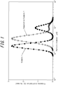
- a curve indicating the frequency distribution obtained through particle size distribution measurement had a fine particle peak having a peak top at a particle diameter of 20 nm and a coarse particle peak having a peak top at a particle diameter of 100 nm.
- the frequency distribution obtained through particle size distribution measurement of the titanium dioxide nanoparticles in the titanium dioxide paste is illustrated in FIG. 1 .
- a ratio of the frequencies at the peak tops was more than 1/3.
- a transparent conductive plastic film (thickness: 200 ⁇ m; conductive layer-side surface resistance: 15 ⁇ /sq.) including a conductive layer formed of ITO on a base material made of PET was prepared.
- a silver dispersion paste was patterned on the conductive layer in a parallel line form with a line width of 100 ⁇ m, a thickness of 20 ⁇ m, and a spacing of 10 mm by screen printing so as to form auxiliary lead lines for current collection formed of silver.
- a polyester resin was applied as a protective film onto these auxiliary lead lines for current collection with a width of 250 ⁇ m and a thickness of 4 ⁇ m so as to completely protect the auxiliary lead lines for current collection.
- a surface resistance value at the conductive layer-side of the transparent conductive plastic film on which the auxiliary lead lines for current collection had been formed was 3 ⁇ /sq.
- the transparent conductive plastic film on which these auxiliary lead lines for current collection had been formed was cut to 2 cm ⁇ 10 cm to obtain a conductive substrate, a pattern in which 6 circles of 6 mm in diameter were arranged with a spacing of 1.5 cm was printed on a surface at the conductive layer-side of this conductive substrate by screen printing using the titanium dioxide paste described above and a 200-mesh screen, and heated drying (10 minutes at 150°C) was subsequently performed to form a porous semiconductor layer having a film thickness of 8.2 ⁇ m. In this manner, a porous semiconductor electrode substrate having a porous semiconductor layer formed on the surface at the conductive layer-side of the conductive substrate was obtained.
- the porous semiconductor layer formed on the porous semiconductor electrode substrate was used to measure and evaluate light transmittance, close adherence with the conductive substrate, and peeling durability. The results are shown in Table 1.
- the porous semiconductor electrode substrate was immersed in a sensitizing dye solution obtained by dissolving a tetrabutyl ammonium salt of a bis(isocyanate) bis(bipyridyl) Rh complex (N719) as a Ru bipyridyl complex dye in a mixed solvent of acetonitrile:tert-butanol (1:1 (volume ratio)) such as to have a concentration of 3 ⁇ 10 -4 mol/L and was left at 40°C under stirring for 60 minutes to cause adsorption of the dye to the porous semiconductor layer of the porous semiconductor electrode substrate, and thereby produce a dye-sensitized electrode (photoelectrode).
- a sensitizing dye solution obtained by dissolving a tetrabutyl ammonium salt of a bis(isocyanate) bis(bipyridyl) Rh complex (N719) as a Ru bipyridyl complex dye in a mixed solvent of acetonitrile:ter
- the photoelectrode was cut to 2 cm ⁇ 1.5 cm such that a porous semiconductor layer having a circular shape of 6 mm in diameter was at the center thereof.
- the counter electrode was also cut to 2 cm ⁇ 1.5 cm, and then an injection opening (diameter: 1 mm) for electrolyte solution was formed.
- the photoelectrode and the counter electrode were overlapped with an ionomer resin film (Himilan 1652 produced by Dupont-Mitsui Polychemicals Co., Ltd.) of 25 ⁇ m in thickness interposed therebetween in a state in which the surface at the porous semiconductor layer-side of the photoelectrode where the dye had adsorbed and the surface at the conductive layer-side of the counter electrode faced each other, and were subjected to 5 minutes of curing treatment at 110°C.
- ionomer resin film Himilan 1652 produced by Dupont-Mitsui Polychemicals Co., Ltd.
- a titanium dioxide paste, a porous semiconductor electrode substrate, and a dye-sensitized solar cell were produced, and various measurements and evaluations were performed in the same way as in Example 1 with the exception that in production of the titanium dioxide paste in Example 1, the pH of the aqueous sol containing the titanium dioxide nanoparticles D was changed from 2.6 to 2.9 so as to change the pH of the obtained titanium dioxide paste from 2.9 to 3.1.
- the results are shown in Table 1.
- the obtained titanium dioxide paste had a pH of 3.7. Note that the average particle diameter of the titanium dioxide nanop
- a curve indicating a frequency distribution obtained through particle size distribution measurement of titanium dioxide nanoparticles in the titanium dioxide paste had a fine particle peak having a peak top at a particle diameter of 38 nm and a coarse particle peak having a peak top at a particle diameter of 112 nm.
- the frequency distribution of the titanium dioxide nanoparticles in the titanium dioxide paste is illustrated in FIG. 1 .
- a ratio of the frequencies at the peak tops was not more than 1/3.
- a titanium dioxide paste, a porous semiconductor electrode substrate, and a dye-sensitized solar cell were produced, and various measurements and evaluations were performed in the same way as in Comparative Example 1 with the exception that in production of the titanium dioxide paste in Comparative Example 1, the pH of the aqueous sol containing the titanium dioxide nanoparticles E was changed from 3.2 to 3.7 so as to change the pH of the obtained titanium dioxide paste from 3.7 to 4.1.
- the results are shown in Table 1.
- a titanium dioxide paste, a porous semiconductor electrode substrate, and a dye-sensitized solar cell were produced, and various measurements and evaluations were performed in the same way as in Comparative Example 1 with the exception that in production of the titanium dioxide paste in Comparative Example 1, the pH of the aqueous sol containing the titanium dioxide nanoparticles E was changed from 3.2 to 4.0 so as to change the pH of the obtained titanium dioxide paste from 3.7 to 4.5.
- the results are shown in Table 1.
- a porous semiconductor layer having excellent close adherence with a conductive substrate can be formed using the titanium dioxide pastes of Examples 1 and 2, which each contain titanium dioxide nanoparticles and water and have a pH within the prescribed range.
- a titanium dioxide paste that can form a porous semiconductor layer having excellent close adherence with a conductive substrate.
- porous semiconductor electrode substrate having excellent close adherence of a porous semiconductor layer and a conductive substrate.
Landscapes
- Engineering & Computer Science (AREA)
- Chemical & Material Sciences (AREA)
- Power Engineering (AREA)
- Organic Chemistry (AREA)
- Microelectronics & Electronic Packaging (AREA)
- Environmental & Geological Engineering (AREA)
- Life Sciences & Earth Sciences (AREA)
- General Life Sciences & Earth Sciences (AREA)
- Geology (AREA)
- Inorganic Chemistry (AREA)
- Materials Engineering (AREA)
- Hybrid Cells (AREA)
- Photovoltaic Devices (AREA)
- Inorganic Compounds Of Heavy Metals (AREA)
Abstract
Description
- The present disclosure relates to a titanium dioxide paste, a porous semiconductor electrode substrate, a photoelectrode, and a dye-sensitized solar cell.
- In recent years, solar cells have been attracting interest as photoelectric conversion elements that convert light energy to electrical power. Among solar cells, dye-sensitized solar cells are attracting interest for reasons such as that they can be expected to have lighter weight than silicon solar cells and the like, they can generate electricity stably over a wide illuminance range, and they can be produced using comparatively cheap materials without the need for large scale equipment.
- A dye-sensitized solar cell normally has a structure in which a dye-sensitized electrode (photoelectrode), an electrolyte layer, and a counter electrode including a catalyst layer are arranged in this order.
- A dye-sensitized electrode included in a dye-sensitized solar cell is produced by, for example, forming a porous semiconductor layer formed of semiconductor nanoparticles such as titanium dioxide nanoparticles on a conductive substrate to produce a porous semiconductor electrode substrate, and then causing adsorption of a sensitizing dye or the like to the porous semiconductor layer.
- The conductive substrate used in production of the porous semiconductor electrode substrate may, for example, be a substrate that is obtained by forming a conductive layer formed of a conductive material such as indium-tin complex oxide (ITO) on a support (base material) formed of an inorganic material (for example, glass) or an organic material (for example, plastic).
- In a case in which a conductive substrate that includes a support formed of an inorganic material such as glass is used, a porous semiconductor layer can be formed on the conductive substrate by implementing an application step of applying a paste (or viscous dispersion liquid) that contains semiconductor nanoparticles and a binder for thickening onto the conductive substrate and subsequently implementing a baking step of baking at high-temperature (450°C or higher) to burn off the binder.
- An organic material such as a plastic may be used as a support of a conductive substrate instead of an inorganic material such as glass from a viewpoint of producing a dye-sensitized solar cell having excellent flexibility.
- In a case in which a conductive substrate that includes a support formed of an organic material such as a plastic is used, it is necessary for a porous semiconductor layer to be formed on the conductive substrate at a low temperature (for example, 160°C or lower) that is within a heat resistant temperature range of the organic material.
- For example, Patent Literature (PTL) 1 reports that when a viscous dispersion liquid that contains water as a dispersion medium, anatase crystalline titanium dioxide nanoparticles having an average particle diameter within a specific range, and brookite crystalline titanium dioxide nanoparticles having an average particle diameter within a specific range and that has a solid content concentration and viscosity that are within specific ranges is used as the paste mentioned above, it is possible to accurately form a porous semiconductor layer on a conductive substrate including a support formed of a plastic (for example, on a transparent conductive plastic film) at low-temperature.
- PTL 1:
WO2016/006227A1 - In dye-sensitized solar cells, there are instances in which electrolyte solution erodes an interface between a porous semiconductor layer and a conductive substrate and thereby causes peeling of the porous semiconductor layer from the conductive substrate. From a viewpoint of inhibiting peeling of the porous semiconductor layer from the conductive substrate in this manner, it is necessary for the porous semiconductor layer to have good close adherence with the conductive substrate.
- However, there is room for improvement of a porous semiconductor layer formed according to the conventional technique described above in terms of close adherence with a conductive substrate.
- Accordingly, one object of the present disclosure is to provide a titanium dioxide paste that can form a porous semiconductor layer having excellent close adherence with a conductive substrate.
- Another object of the present disclosure is to provide a porous semiconductor electrode substrate having excellent close adherence of a porous semiconductor layer and a conductive substrate.
- Yet another object of the present disclosure is to provide a photoelectrode and a dye-sensitized solar cell that include this porous semiconductor electrode substrate.
- The inventor conducted diligent investigation with the aim of solving the problem set forth above. The inventor discovered that a porous semiconductor layer having excellent close adherence with a conductive substrate can be formed by using a titanium dioxide paste that contains titanium dioxide nanoparticles and water and that has a pH within a specific range, and, in this manner, the inventor completed the present disclosure.
- Specifically, the present disclosure aims to advantageously solve the problem set forth above, and a presently disclosed titanium dioxide paste comprises titanium dioxide nanoparticles and water, and has a pH of not lower than 2.6 and not higher than 3.5. When a titanium dioxide paste contains titanium dioxide nanoparticles and water and has a pH within the specific range set forth above in this manner, the titanium dioxide paste can form a porous semiconductor layer having excellent close adherence with a conductive substrate.
- For the presently disclosed titanium dioxide paste, it is preferable that a curve indicating a frequency distribution obtained through particle size distribution measurement, by mass, of the titanium dioxide nanoparticles has at least two peaks. When a curve indicating a frequency distribution obtained through particle size distribution measurement, by mass, of the titanium dioxide nanoparticles has at least two peaks in this manner, close adherence of a porous semiconductor layer and a conductive substrate can be further increased, and photoelectric conversion efficiency of a dye-sensitized solar cell can be increased.
- Note that the curve indicating a frequency distribution obtained through particle size distribution measurement, by mass, of the titanium dioxide nanoparticles is obtained through measurement of the presently disclosed titanium dioxide paste by ultrasound attenuation spectroscopy.
- The reason that close adherence of a porous semiconductor layer and a conductive substrate can be further increased and photoelectric conversion efficiency of a dye-sensitized solar cell can be increased as a result of at least two peaks being present on the curve indicating a frequency distribution obtained through particle size distribution measurement, by mass, of the titanium dioxide nanoparticles is as follows. In a situation in which the curve indicating a frequency distribution obtained through particle size distribution measurement has two peaks that are a peak corresponding to coarse particles and a peak corresponding to fine particles, for example, the fine particles pack into gaps between the coarse particles such that a porous semiconductor layer having a high level of packing is obtained. As a result, contact between the porous semiconductor layer and a conductive substrate is a state similar to surface contact, rather than point contact, and close adherence between the porous semiconductor layer and the conductive substrate improves. Moreover, improvement of packing of the porous semiconductor layer can increase photoelectric conversion efficiency of a dye-sensitized solar cell by inhibiting transmission of sunlight and enabling effective use of sunlight.
- For the presently disclosed titanium dioxide paste, it is preferable that the at least two peaks include a fine particle peak having a peak top at a particle diameter of not less than 10 nm and not more than 40 nm and a coarse particle peak having a peak top at a particle diameter of not less than 60 nm and not more than 200 nm. When the at least two peaks include a fine particle peak and a coarse particle peak having peak tops within the specific ranges set forth above in this manner, close adherence of a porous semiconductor layer and a conductive substrate can be even further increased, and photoelectric conversion efficiency of a dye-sensitized solar cell can be further increased.
- For the presently disclosed titanium dioxide paste, it is preferable that a ratio of frequency at the peak top of the coarse particle peak relative to frequency at the peak top of the fine particle peak (frequency at peak top of coarse particle peak/frequency at peak top of fine particle peak) is more than 1/3. When a ratio of the frequency at the peak top of the coarse particle peak and the frequency at the peak top of the fine particle peak (frequency at peak top of coarse particle peak/frequency at peak top of fine particle peak) is more than the specific value set forth above in this manner, close adherence of a porous semiconductor layer and a conductive substrate can be even further increased, and photoelectric conversion efficiency of a dye-sensitized solar cell can be even further increased.
- Note that the ratio of the frequencies at the peak tops (frequency at peak top of coarse particle peak/frequency at peak top of fine particle peak) can be calculated from a ratio of the heights of the respective peak tops of the coarse particle peak and the fine particle peak.
- The presently disclosed titanium dioxide paste preferably has a solid content concentration of not less than 45 mass% and not more than 55 mass%. When the solid content concentration of the titanium dioxide paste is within the specific range set forth above in this manner, the titanium dioxide paste can be provided with suitable viscosity (rheological properties and thixotropy), and screen printing properties of the titanium dioxide paste can be enhanced.
- Note that the solid content concentration of the titanium dioxide paste can be measured by mass loss on drying (drying at 180°C for 1 hour). Moreover, the solid content concentration of the titanium dioxide paste can be calculated from the specific gravity of each component contained in the titanium dioxide paste and the specific gravity of the titanium dioxide paste measured using a specific gravity cup.
- The presently disclosed titanium dioxide paste preferably has a viscosity at 25°C of not less than 10 Pa·s and not more than 24 Pa·s. When the viscosity at 25°C of the titanium dioxide paste is within the specific range set forth above in this manner, the titanium dioxide paste can be provided with suitable viscosity (rheological properties and thixotropy), and screen printing properties of the titanium dioxide paste can be enhanced.
- Note that the viscosity at 25°C of the titanium dioxide paste can be measured by a method described in the EXAMPLES section of the present specification.
- The presently disclosed titanium dioxide paste preferably does not substantially comprise a binder. When the titanium dioxide paste does not substantially contain a binder in this manner, electrical conductivity of a porous semiconductor layer can be increased.
- Moreover, the present disclosure aims to advantageously solve the problem set forth above, and a presently disclosed porous semiconductor electrode substrate comprises: a conductive substrate; and a porous semiconductor layer formed by applying any one of the titanium dioxide pastes set forth above onto the conductive substrate and drying the titanium dioxide paste that has been applied. A porous semiconductor electrode substrate that is obtained by applying any one of the titanium dioxide pastes set forth above onto a conductive substrate and drying the applied titanium dioxide paste to form a porous semiconductor layer in this manner has excellent close adherence of the porous semiconductor layer and the conductive substrate.
- Furthermore, the present disclosure aims to advantageously solve the problem set forth above, and a presently disclosed photoelectrode comprises: the porous semiconductor electrode substrate set forth above; and a dye or light-absorbing material adsorbed to the porous semiconductor layer of the porous semiconductor electrode substrate. A photoelectrode that includes the porous semiconductor electrode substrate set forth above in this manner has excellent close adherence of a porous semiconductor layer and a conductive substrate.
- Also, the present disclosure aims to advantageously solve the problem set forth above, and a presently disclosed dye-sensitized solar cell comprises the porous semiconductor electrode substrate set forth above. A dye-sensitized solar cell that includes the porous semiconductor electrode substrate set forth above in this manner has excellent close adherence of a porous semiconductor layer and a conductive substrate and high performance.
- According to the present disclosure, it is possible to provide a titanium dioxide paste that can form a porous semiconductor layer having excellent close adherence with a conductive substrate.
- Moreover, according to the present disclosure, it is possible to provide a porous semiconductor electrode substrate having excellent close adherence of a porous semiconductor layer and a conductive substrate.
- Furthermore, according to the present disclosure, it is possible to provide a photoelectrode and a dye-sensitized solar cell that include this porous semiconductor electrode substrate.
- In the accompanying drawing,
-
FIG. 1 is a graph of curves indicating frequency distribution by mass (vertical axis) against particle diameter (horizontal axis) for titanium dioxide nanoparticles in titanium dioxide pastes of Example 1 and Comparative Example 1. - The following provides a detailed description of embodiments of the present disclosure.
- The presently disclosed titanium dioxide paste can be used in production of the presently disclosed porous semiconductor electrode substrate. Moreover, the presently disclosed porous semiconductor electrode substrate includes a porous semiconductor layer formed using the presently disclosed titanium dioxide paste. Furthermore, the presently disclosed porous semiconductor electrode substrate can be used in production of a presently disclosed photoelectrode for a dye-sensitized solar cell. Also, the presently disclosed dye-sensitized solar cell includes the presently disclosed porous semiconductor electrode substrate.
- Features of the presently disclosed titanium dioxide paste are that it contains titanium dioxide nanoparticles and water and has a pH within a specific range. The presently disclosed titanium dioxide paste makes it possible to form a porous semiconductor layer having excellent close adherence with a conductive substrate. Therefore, by using a porous semiconductor layer that has been formed using the presently disclosed titanium dioxide paste, it becomes difficult for electrolyte solution to erode an interface between the porous semiconductor layer and a conductive substrate in a dye-sensitized solar cell, and peeling of the porous semiconductor layer from the conductive substrate can be inhibited.
- Note that the term "paste" as used in the present specification refers to a dispersion in which solid particles are dispersed in a liquid such as water serving as a dispersion medium, and that has fluidity and high viscosity.
- In the presently disclosed titanium dioxide paste, it is normally the case that the titanium dioxide nanoparticles, which are solid particles, are dispersed in water serving as a dispersion medium.
- Note that the presently disclosed titanium dioxide paste may optionally contain other components besides the titanium dioxide nanoparticles and water mentioned above.
- The titanium dioxide nanoparticles contained in the titanium dioxide paste are a component that can function as a semiconductor in a porous semiconductor electrode substrate included in a dye-sensitized solar cell.
- The number of peaks present on a curve indicating a frequency distribution obtained through particle size distribution measurement, by mass, of the titanium dioxide nanoparticles is normally two or more, and is preferably two. When the number of peaks present on the curve indicating a frequency distribution obtained through particle size distribution measurement, by mass, of the titanium dioxide nanoparticles is two or more, it is possible to densify a porous semiconductor layer and further increase close adherence of the porous semiconductor layer and a conductive substrate, and it is also possible to reduce transmittance of the porous semiconductor layer and increase photoelectric conversion efficiency of a dye-sensitized solar cell.
- Note that the curve indicating a frequency distribution obtained through particle size distribution measurement, by mass, of the titanium dioxide nanoparticles is obtained through measurement of the presently disclosed titanium dioxide paste by ultrasound attenuation spectroscopy.
- In this ultrasound attenuation spectroscopy, the titanium dioxide paste is irradiated with ultrasound to cause relative motion of the titanium dioxide nanoparticles in the titanium dioxide paste relative to the dispersion medium, such as water. The attenuation rate of sound energy caused by this relative motion is measured relative to generated sound energy, and a particle size distribution is determined from a characteristic thereof.
- More specifically, the titanium dioxide paste is irradiated with ultrasound of a certain frequency from one oscillator, ultrasound is received by another oscillator at the opposite side, and the proportion of ultrasound that is attenuated therebetween (i.e., the attenuation rate) is measured. In order to increase the reliability of measured values, measurement is performed with varying distance between the oscillators, and an attenuation rate per unit amount is calculated. Theoretical curve fitting is then performed with respect to an obtained spectrum of ultrasound frequency vs attenuation rate to obtain a curve indicating a frequency distribution according to particle size distribution measurement, by mass, of the titanium dioxide nanoparticles.
- Note that the term "peak" as used in the present specification refers to "a section protruding relative to the baseline", and the term "peak top" as used in the present specification refers to "a point on a peak where a maximum value of frequency distribution according to particle size distribution measurement is displayed".
- In a case in which the curve indicating a frequency distribution obtained through particle size distribution measurement, by mass, of the titanium dioxide nanoparticles has two or more peaks, the two or more peaks preferably include a fine particle peak having a peak top at a particle diameter of not less than 10 nm and not more than 40 nm and a coarse particle peak having a peak top at a particle diameter of not less than 60 nm and not more than 200 nm. When the two or more peaks of the curve indicating a frequency distribution obtained through particle size distribution measurement, by mass, of the titanium dioxide nanoparticles include a fine particle peak and a coarse particle peak having peak tops within the specific ranges set forth above in this manner, close adherence of a porous semiconductor layer and a conductive substrate can be even further increased, and photoelectric conversion efficiency of a dye-sensitized solar cell can be further increased.
- Note that the range for the peak top of the fine particle peak is preferably a particle diameter of not less than 15 nm and not more than 25 nm and the range for the peak top of the coarse particle peak is preferably a particle diameter of not less than 80 nm and not more than 120 nm from a viewpoint of causing good packing of fine particles between coarse particles so as to increase packing of a porous semiconductor layer.
- Moreover, a ratio of the frequencies at the peak tops described above (frequency at peak top of coarse particle peak/frequency at peak top of fine particle peak) is preferably more than 1/3. When the ratio of the frequency at the peak top of the coarse particle peak and the frequency at the peak top of the fine particle peak (frequency at peak top of coarse particle peak/frequency at peak top of fine particle peak) is more than the specific value set forth above in this manner, close adherence of a porous semiconductor layer and a conductive substrate can be even further increased, and photoelectric conversion efficiency of a dye-sensitized solar cell can be further increased.
- The average particle diameter of the titanium dioxide nanoparticles in the titanium dioxide paste is preferably 5 nm or more, and more preferably 22 nm or more, and is preferably 80 nm or less.
- Note that unless otherwise specified, the term "average particle diameter" as used in the present specification represents the particle diameter (D50) at which, in a frequency distribution based on a particle size distribution by mass measured by ultrasound attenuation spectroscopy, cumulative mass calculated from a small diameter end of the distribution reaches 50%.
- The titanium dioxide nanoparticles may be crystalline. In a case in which the titanium dioxide nanoparticles are crystalline, the crystal structure may be anatase, brookite, rutile, or the like, for example, without any specific limitations.
- The particle shape of the titanium dioxide nanoparticles can be an undefined shape, a spherical shape, a polyhedral shape, a fibrous shape, a nanotube shape, or the like, for example, without any specific limitations.
- No specific limitations are placed on the state of titanium dioxide nanoparticles that are used to produce the titanium dioxide paste. For example, titanium dioxide nanoparticles may be used in a powder state or may be used in the state of a sol (dispersion liquid) having the titanium dioxide nanoparticles dispersed in a dispersion medium such as water.
- The crystal structure, particle shape, state, and so forth of the titanium dioxide nanoparticles described above can differ depending on the production method of the titanium dioxide nanoparticles.
- Examples of production methods of titanium dioxide nanoparticles that can be used include, but are not specifically limited to, a liquid phase method in which a titanium compound such as titanium tetrachloride or titanyl sulfate is hydrolyzed and a gas phase method in which mixed combustion of titanium tetrachloride and oxygen or an oxygen-containing gas is performed. Note that various conditions in the production method of the titanium dioxide nanoparticles can be set as appropriate within ranges with which the desired effects are obtained.
- Moreover, the production method of the titanium dioxide nanoparticles may be a single production method, but is preferably a method in which a plurality of types of titanium dioxide nanoparticles differing in terms of crystal structure, particle shape, state, and/or the like that are obtained by different production methods are mixed in any proportions.
- Moreover, by appropriately adjusting conditions for the proportions in which the plurality of types of titanium dioxide nanoparticles are mixed, for example, titanium dioxide nanoparticles displaying the frequency distribution described above can easily be produced as a mixture.
- Also note that the production method of the titanium dioxide nanoparticles may be implemented as part of a production method of the titanium dioxide paste.
- The presently disclosed titanium dioxide paste contains water as a dispersion medium for dispersing the titanium dioxide nanoparticles described above. Note that in a situation in which an aqueous sol having titanium dioxide nanoparticles dispersed in water is used in production of the titanium dioxide paste, water contained in this aqueous sol may be used in that form as the water contained in the titanium dioxide paste.
- The presently disclosed titanium dioxide paste may also contain another dispersion medium besides water with the aim of adjusting viscosity and improving drying properties.
- No specific limitations are placed on the other dispersion medium so long as the desired effects are obtained, and examples thereof include ethylene glycol mono-tert-butyl ether, diacetone alcohol, and linear and branched alcohols having a carbon number of 3 to 10 described in
WO2016/006227A1 . - Note that the content of the other dispersion medium in the presently disclosed titanium dioxide paste can be adjusted as appropriate within a range with which the desired effects are obtained.
- In a case in which water and another dispersion medium are used together as a dispersion medium, the proportional content of water in the dispersion medium is preferably 80 mass% or more, and more preferably 83 mass% or more, and is preferably 90 mass% or less, and more preferably 87 mass% or less.
- The presently disclosed titanium dioxide paste may contain other components besides the titanium dioxide nanoparticles and water described above. Examples of such other components include binders, particles other than titanium dioxide nanoparticles, and acids.
- Although the presently disclosed titanium dioxide paste may contain a binder formed of a resin or the like with the aim of viscosity enhancement, for example, the presently disclosed titanium dioxide paste preferably does not substantially contain a binder. When the presently disclosed titanium dioxide paste does not substantially contain a binder, a binder does not remain in a porous semiconductor layer formed using the titanium dioxide paste even in a situation in which the porous semiconductor layer is formed at low-temperature (for example, 150°C or lower), and thus sufficiently high electrical conductivity of the porous semiconductor layer can be ensured.
- Note that the phrase "does not substantially contain a binder" means that the content of organic material having a boiling point of 150°C or higher at a pressure of 1 atm is 1 mass% or less in terms of solid content. Also note that the content of organic material having a boiling point of 150°C or higher at a pressure of 1 atm is preferably 0.5 mass% or less in terms of solid content, and is more preferably 0 mass%.
- The presently disclosed titanium dioxide paste may contain other particles besides the titanium dioxide nanoparticles described above.
- No specific limitations are placed on other particles that can be used so long as the desired effects are obtained, and examples include particles of semiconductors other than titanium dioxide, inorganic compounds other than semiconductors, and so forth such as described in
WO2016/006227A1 . - Note that the content of the other particles in the presently disclosed titanium dioxide paste can be adjusted as appropriate within a range with which the desired effects are obtained.
- The presently disclosed titanium dioxide paste may contain an acid with the aim of pH adjustment.
- Specific examples of acids that can be used include hydrochloric acid and the like, though no specific limitations are made so long as the desired effects are obtained.
- In a situation in which an aqueous sol having titanium dioxide nanoparticles dispersed in water is used in production of the titanium dioxide paste, an acid such as hydrochloric acid that may be contained in the aqueous sol as a residue can be used in that form as an acid contained in the titanium dioxide paste. Moreover, a separate acid to the aforementioned aqueous sol may be added during mixing of components in production of the titanium dioxide paste.
- Note that the content of an acid in the titanium dioxide paste is preferably adjusted as appropriate such that the pH of the titanium dioxide paste is within a specific range described below.
- The pH of the presently disclosed titanium dioxide paste is required to be 2.6 or higher, and is preferably 2.7 or higher, more preferably 2.8 or higher, and even more preferably 2.9 or higher. Moreover, the pH of the presently disclosed titanium dioxide paste is required to be 3.5 or lower, and is preferably 3.3 or lower, more preferably 3.1 or lower, and even more preferably 3.0 or lower. When the pH of the titanium dioxide paste is not lower than any of the lower limits set forth above, it is possible to sufficiently increase the viscosity of the titanium dioxide paste and maintain good screen printing properties, and it is also possible to inhibit excessive erosion of a conductive substrate and ensure sufficiently high electrical conductivity of a porous semiconductor electrode substrate. On the other hand, when the pH of the titanium dioxide paste is not higher than any of the upper limits set forth above, a porous semiconductor layer having excellent close adherence with a conductive substrate can be formed through a suitable degree of erosion of the conductive substrate. Moreover, when the pH of the titanium dioxide paste is not higher than any of the upper limits set forth above, it is possible to increase dispersibility of the titanium dioxide nanoparticles in the titanium dioxide paste and maintain good screen printing properties of the titanium dioxide paste, and it is also possible to increase light absorbance (reduce transmittance) of a porous semiconductor layer and maintain good performance, such as photoelectric conversion efficiency, of a dye-sensitized solar cell (DSC).
- Note that the method of adjustment of the pH of the titanium dioxide paste is described further below in relation to the production method of the titanium dioxide paste.
- The solid content concentration of the presently disclosed titanium dioxide paste is preferably 45 mass% or more, and more preferably 48 mass% or more, and is preferably 55 mass% or less, and more preferably 52 mass% or less. When the solid content concentration of the titanium dioxide paste is within any of the specific ranges set forth above, screen printing properties of the titanium dioxide paste can be enhanced.
- Note that the proportion constituted by the titanium dioxide nanoparticles among solid content in the presently disclosed titanium dioxide paste is preferably not less than 99 mass% and not more than 100 mass%.
- The viscosity at 25°C of the presently disclosed titanium dioxide paste is preferably 10 Pa·s or more, and more preferably 13 Pa·s or more, and is preferably 24 Pa·s or less, and more preferably 20 Pa·s of less. When the viscosity at 25°C of the titanium dioxide paste is within any of the specific ranges set forth above, screen printing properties of the titanium dioxide paste can be enhanced.
- Note that the viscosity at 25°C of the titanium dioxide paste can be adjusted through the solid content concentration of the titanium dioxide paste, for example.
- The production method of the titanium dioxide paste is not specifically limited and can, for example, be a method in which a powder of titanium dioxide nanoparticles and other optional components are added to and mixed with an aqueous sol having titanium dioxide nanoparticles dispersed in water, and then a dispersing device is used to disperse components such as the powder of titanium dioxide nanoparticles in the aqueous sol.
- The water contained in the aqueous sol can be used in that form as the water that is contained in the titanium dioxide paste. Moreover, water that is separate to the aqueous sol may be added in the operations described above.
- The dispersing device can be a commonly known dispersing device such as a three-roll mill, a paint conditioner, a homogenizer, an ultrasonic stirrer, a high-speed disper blade, or a combined rotation and revolution mixing conditioner.
- No specific limitations are placed on the method by which the pH of the titanium dioxide paste is adjusted. For example, the pH of the titanium dioxide paste can be adjusted to within any of the specific ranges set forth above through appropriate setting of the pH of the aqueous sol.
- The presently disclosed porous semiconductor electrode substrate includes a conductive substrate and a porous semiconductor layer formed by applying the titanium dioxide paste set forth above onto the conductive substrate and performing heated drying of the titanium dioxide paste that has been applied.
- As a result of the presently disclosed porous semiconductor electrode substrate including a porous semiconductor layer formed using the presently disclosed titanium dioxide paste set forth above on a conductive substrate, the presently disclosed porous semiconductor electrode substrate has excellent close adherence of the porous semiconductor layer and the conductive substrate.
- The conductive substrate can, for example, be a substrate that is itself electrically conductive, such as a metal substrate formed of a metal material such as titanium or stainless steel; or a substrate obtained by forming a conductive layer on a base material (support) formed of a material such as an inorganic material (for example, glass) or an organic material (for example, plastic). Note that the material of the conductive substrate can be selected as appropriate depending on the application of the porous semiconductor electrode substrate and may be a transparent material in a case in which the porous semiconductor electrode substrate is required to have light transmittivity, for example.
- From a viewpoint of producing a dye-sensitized solar cell having excellent flexibility, it is preferable to use a conductive substrate including a support formed of a flexible plastic, and particularly preferable to use a conductive substrate including a transparent plastic film as a support (i.e., to use a transparent conductive plastic film).
- A transparent conductive plastic film includes a transparent plastic film as a support and a conductive layer formed on the transparent plastic film. The transparent plastic film serving as a support is preferably formed of a low cost material that is colorless and that has excellent transparency, heat resistance, chemical resistance, and gas barrier properties. Examples of materials for the transparent plastic film serving as a support that are preferable from such viewpoints include polyethylene terephthalate (PET), polyethylene naphthalate (PEN), syndiotactic polystyrene (SPS), polyphenylene sulfide (PPS), polycarbonate (PC), polyarylate (PAr), polysulfone (PSF), polyester sulfone (PES), polyetherimide (PEI), and transparent polyimide (PI). Of these materials, polyethylene terephthalate (PET) and polyethylene naphthalate (PEN) are preferable from viewpoints of chemical resistance, cost, and so forth.
- In the conductive layer of the transparent conductive plastic film, a metal such as platinum, gold, silver, copper, aluminum, or indium; a carbon-based material such as carbon nanotubes; a conductive metal oxide such as indium-tin complex oxide or tin oxide; or the like can be used as a conductive material. Of these materials, a conductive metal oxide is preferable from a viewpoint of optical transparency, with indium-tin complex oxide (ITO) and zinc oxide being particularly preferable. The transmittance of indium-tin complex oxide (ITO) preferably has a peak at 500 nm to 600 nm from a viewpoint of photoelectric conversion efficiency and visibility of a display or the like.
- A surface resistance value of the conductive layer is preferably 20 Ω/sq. or less, more preferably 10 Ω/sq. or less, and even more preferably 3 Ω/sq. or less.
- Auxiliary lead lines can be provided on the conductive layer by patterning or the like for the purpose of current collection. Such auxiliary lead lines are normally formed using a low-resistance metal material such as copper, silver, aluminum, platinum, gold, titanium, or nickel. In the case of a conductive layer that is patterned with such auxiliary lead lines, the surface resistance value is measured as a resistance value of the surface where an auxiliary lead line is included, and this value is preferably 10 Ω/sq. or less, and more preferably 3 Ω/sq. or less.
- The thickness of the transparent conductive plastic film is preferably not less than 30 µm and not more than 500 µm. When the thickness of the transparent conductive plastic film is not less than the lower limit set forth above, the transparent conductive plastic film has excellent handleability, and deformation is inhibited during drying in formation of the porous semiconductor layer.
- The presently disclosed porous semiconductor electrode substrate can be produced by applying the presently disclosed titanium dioxide paste set forth above onto the conductive substrate and drying the titanium dioxide paste that has been applied to form a porous semiconductor layer. The porous semiconductor layer that is formed on the conductive substrate has excellent close adherence with the conductive substrate and peeling durability.
- The method by which the presently disclosed titanium dioxide paste set forth above is applied onto the conductive substrate can be a screen printing method, a metal mask method, a gravure printing method, or the like, for example, of which, a screen printing method is preferable. Note that the presently disclosed titanium dioxide paste can be diluted and then applied onto the conductive substrate by a method such as a doctor blading method, a squeegee method, or a spraying method.
- In a case in which a substrate obtained by forming a conductive layer on a base material (support) formed of a material such as a plastic is used as the conductive substrate (for example, a case in which a transparent conductive plastic film is used), the porous semiconductor layer is formed by applying the titanium dioxide paste onto a surface at the conductive layer-side of the conductive substrate.
- The titanium dioxide paste that has been applied can be dried by performing heated drying, for example, but is not specifically limited to being dried in this manner.
- The heating temperature in heated drying can be set as appropriate within a heat resistant temperature range of a constituent material of the conductive substrate that is used. For example, in a case in which a conductive substrate including a support formed of a plastic, such as the previously described transparent conductive plastic film, is used, the heating temperature in heated drying is preferably not lower than 120°C and not higher than 160°C from a viewpoint of performing drying efficiently while also inhibiting degradation of the plastic serving as the support caused by heating.
- The thickness of the formed porous semiconductor layer is preferably not less than 5 µm and not more than 10 µm. When the thickness of the porous semiconductor layer is not less than the lower limit set forth above, sufficiently high electricity generation by a dye-sensitized solar cell can be ensured. On the other hand, when the thickness of the porous semiconductor layer is not more than the upper limit set forth above, sufficiently high diffusivity of electrons in the porous semiconductor layer can be ensured.
- The presently disclosed photoelectrode includes the porous semiconductor electrode substrate set forth above and a dye or light-absorbing material adsorbed to the porous semiconductor layer of the porous semiconductor electrode substrate. The presently disclosed photoelectrode has excellent close adherence of a porous semiconductor layer and a conductive substrate as a result of including the porous semiconductor electrode substrate set forth above.
- The dye or light-absorbing material adsorbed to the porous semiconductor layer of the porous semiconductor electrode substrate is not specifically limited and can, for example, be a dye or light-absorbing material described in
WO2016/006227A1 . - The presently disclosed dye-sensitized solar cell includes the porous semiconductor electrode substrate set forth above. The presently disclosed dye-sensitized solar cell has excellent close adherence of a porous semiconductor layer and a conductive substrate and high performance as a result of including the porous semiconductor electrode substrate set forth above.
- More specifically, the presently disclosed dye-sensitized solar cell includes a dye-sensitized electrode (photoelectrode) in which a dye or light-absorbing material is adsorbed to the porous semiconductor layer of the porous semiconductor electrode substrate set forth above, a counter electrode, and an electrolyte layer disposed between the dye-sensitized electrode and the counter electrode.
- The dye or light-absorbing material adsorbed to the porous semiconductor layer of the porous semiconductor electrode substrate is not specifically limited and can, for example, be a dye or light-absorbing material such as previously described in the "Photoelectrode" section.
- Moreover, the counter electrode can be a substrate that is obtained by forming a conductive layer on a base material (support) formed of an organic material such as a plastic. The conductive material of the conductive layer included in the counter electrode can be a metal such as platinum, gold, silver, copper, titanium, aluminum, magnesium, or indium; a carbon-based material such as carbon nanotubes; a conductive metal oxide such as indium-tin complex oxide or fluorine-doped tin oxide (FTO); or the like. Of these materials, platinum, titanium, ITO, and carbon-based materials are preferable from a viewpoint of corrosion resistance.
- The electrolyte layer disposed between the dye-sensitized electrode and the counter electrode is not specifically limited and can, for example, be an electrolyte solution such as an aqueous electrolyte solution, an organic solvent electrolyte solution, or an ionic liquid electrolyte solution (molten salt electrolyte solution); a P-type semiconductor; or the like described in
WO2016/006227 A1 . - The presently disclosed dye-sensitized solar cell can be produced by a known method without any specific limitations so long as the porous semiconductor electrode substrate set forth above is used. For example, the presently disclosed dye-sensitized solar cell can be produced using the dye-sensitized electrode (photoelectrode) set forth above. More specifically, the dye-sensitized solar cell can be produced by overlapping the photoelectrode set forth above and a counter electrode, with a spacer interposed therebetween, in a state in which a surface at a side of the photoelectrode where the dye or light-absorbing material is adsorbed to the porous semiconductor layer and a surface at a conductive layer-side of the counter electrode are facing each other, and injecting an electrolyte solution as an electrolyte layer between the photoelectrode and the counter electrode.
- The following provides a more specific description of the present disclosure based on examples. However, the present disclosure is not limited to these examples.
- Various measurements and evaluations in the examples and comparative examples were performed by the following methods.
- The viscosity at 25°C of a titanium dioxide paste can be determined through measurement performed using a B-type viscometer connected to a constant temperature water circulator under conditions of a rotation speed of 50 rpm.
- A transparent conductive plastic film (thickness: 200 µm; conductive layer-side surface resistance: 15 Ω/sq.) having a conductive layer formed of indium-tin complex oxide (ITO) on a base material made of polyethylene terephthalate (PET) was prepared as a conductive substrate. A titanium dioxide paste was applied by screen printing using a 400-mesh screen to a surface of the conductive substrate at a side where the conductive layer had been formed so as to form a rectangular coating film of 5 mm × 33 mm. An arbitrarily selected location of 1 cm2 in the coating film that had been formed was visually inspected, and screen printing properties of the titanium dioxide paste were evaluated in accordance with the following standard. Note that less cissing and fewer pinholes in visual inspection of the coating film indicate that the titanium dioxide paste has better screen printing properties.
- A: Cissing not observed and pinholes of 1 mm or more in diameter not observed
- B: Cissing not observed and 5 or fewer pinholes of 1 mm or more in diameter observed
- C: Cissing not observed and more than 5 pinholes of 1 mm or more in diameter observed
- D: Cissing observed and numerous pinholes of 1 mm or more in diameter also observed
- A DT-1202 produced by Nihon Rufuto Co., Ltd. was used to perform measurement by ultrasound attenuation spectroscopy (ultrasound frequency: 1 MHz to 100 MHz) with respect to a titanium dioxide paste as a measurement sample to obtain a curve indicating a frequency distribution based on a particle size distribution, by mass, of titanium dioxide nanoparticles in the titanium dioxide paste. The number of peaks on the obtained curve indicating the frequency distribution and the particle diameter at which a peak top of each peak was present were confirmed.
- In addition, the particle diameter (D50) at which cumulative mass calculated from a small diameter end in the frequency distribution (by mass) reached 50% was taken to be the average particle diameter of the titanium dioxide nanoparticles in the titanium dioxide paste.
- In a case in which a curve indicating a frequency distribution (by mass) that was obtained as described above had a coarse particle peak and a fine particle peak, a ratio of frequencies at the peak tops (frequency at peak top of coarse particle peak/frequency at peak top of fine particle peak) was calculated based on the heights of the respective peak tops of the coarse particle peak and the fine particle peak.
- A conductive substrate used in production of a porous semiconductor electrode substrate in each example or comparative example was set in an ultraviolet-visible spectrophotometer (UV1800 produced by Shimadzu Corporation) and baseline measurement was performed for a range of 200 nm to 1100 nm. Next, the produced porous semiconductor electrode substrate (having a porous semiconductor layer formed on the conductive substrate) was set in the ultraviolet-visible spectrophotometer, spectroscopic measurement was performed, and a value of light transmittance at 530 nm was determined for the porous semiconductor layer formed on the conductive substrate.
- For each example or comparative example, a produced porous semiconductor electrode substrate (having a porous semiconductor layer formed on a conductive substrate) was cut to a strip shape of 33 mm × 50 mm to produce three test specimens. Each of the test specimens was then placed in a 10 mL sample bottle made of glass. Next, 6 mL of electrolyte solution was loaded into the sample bottle and the lid was closed to seal the sample bottle with the test specimen in an immersed state in the electrolyte solution. The sample bottle was placed in a 60°C thermostatic tank (oven) and was left at rest for 3 days. After 3 days, the test specimen was removed from the sample bottle, and the occurrence or absence of peeling of the porous semiconductor layer from the conductive substrate was visually confirmed for the test specimen.
- Absence of peeling of the porous semiconductor layer from the conductive substrate indicates that the porous semiconductor layer has excellent close adherence with the conductive substrate.
- A solar simulator (PEC-L11 produced by Peccell Technologies Inc.) in which an AM1.5G filter was attached to a 150 W xenon lamp light source was used as a light source. The light intensity was adjusted to 1 sun (AM1.5G, 100 mW/cm2 [Class A of JIS C8912]). A produced dye-sensitized solar cell was connected to a sourcemeter (Series 2400 SourceMeter produced by Keithley Instruments) and the following current/voltage characteristic was measured.
- Output current was measured while changing bias voltage from 0 V to 0.8 V in 0.01 V units under 1 sun light-irradiation. The output current was measured for each voltage step by, after the voltage had been changed, integrating values from 0.05 seconds after the voltage change to 0.15 seconds after the voltage change. Measurement was also performed while changing the bias voltage in the reverse direction from 0.8 V to 0 V, and an average value for the forward direction and the reverse direction was taken to be the photoelectric current.
- Measurement results of the current/voltage characteristic described above were used to calculate the open-circuit voltage (V), the fill factor, and the photoelectric conversion efficiency (%). The short-circuit current density (mA/cm2) was also measured.
- The initial performance of a dye-sensitized solar cell produced in each example or comparative example was evaluated. Next, the dye-sensitized solar cell was loaded into a reliability test tank (IH constant temperature and constant humidity vessel produced by Yamato Scientific Co., Ltd.) that was maintained at a temperature of 60°C and a humidity of 90% RH, and a reliability test was performed by leaving the dye-sensitized solar cell for 500 hours in a light-shielded state without passing of current. The performance of the dye-sensitized solar cell after the reliability test was also evaluated.
- A performance maintenance rate (%) was calculated by the following formula using a current value A1 (mA) measured in evaluation of initial performance of the dye-sensitized solar cell and a current value A2 (mA) measured in evaluation of performance of the dye-sensitized solar cell after the reliability test.

- A larger value for the performance maintenance rate indicates that the dye-sensitized solar cell has better module durability.
- Note that evaluation of performance of the dye-sensitized solar cell, both initially and after the reliability test, was performed by the following method.
- The dye-sensitized solar cell was irradiated with light equivalent to 1 sun of AM1.5G (JIS C 8912) by a solar simulator (PEC-L15 produced by Peccell Technologies Inc.), and the generated current was measured using an interface resistance meter (VSP produced by Bio-Logic Science Instruments) connected to the dye-sensitized solar cell. Current measurement was performed for approximately 10 seconds, an average value was calculated for data of the final 26 points (data for the final 5 seconds) when the value had stabilized, and a value obtained by further multiplying by -1 was taken to be the current value (mA).
- A powder of titanium dioxide nanoparticles A (average particle diameter: 30 nm) and a powder of titanium dioxide nanoparticles B (average particle diameter: 40 nm) were added to an aqueous sol (solid content concentration: 18 mass% to 20 mass%; pH 2.6) having titanium dioxide nanoparticles D (average particle diameter: 12 nm) dispersed in water such as to be mixed with a mass ratio, in terms of solid content, of A:B:D = 47:30:23. Note that the average particle diameters of the titanium dioxide nanoparticles A and B are each a value that was calculated from particle diameter distribution measurement through scanning electron microscope observation. In addition, ethylene glycol mono-tert-butyl ether (EGTBE) and diacetone alcohol (DAA) were added such that the concentrations thereof in a titanium dioxide paste were 4.8 mass% of EGTBE and 1.9 mass% of DAA to thereby obtain a mixture. This mixture was subjected to 10 passes through a desktop three-roll mill to cause dispersion and thereby produce a titanium dioxide paste. The obtained titanium dioxide paste was confirmed to have a pH of 2.9 and a solid content concentration of 49 mass%.
- The viscosity at 25°C and screen printing properties of the titanium dioxide paste were measured and evaluated. The results are shown in Table 1.
- Moreover, a frequency distribution and average particle diameter obtained through particle size distribution measurement of titanium dioxide nanoparticles in the titanium dioxide paste were determined. A curve indicating the frequency distribution obtained through particle size distribution measurement had a fine particle peak having a peak top at a particle diameter of 20 nm and a coarse particle peak having a peak top at a particle diameter of 100 nm. The frequency distribution obtained through particle size distribution measurement of the titanium dioxide nanoparticles in the titanium dioxide paste is illustrated in
FIG. 1 . - Note that a ratio of the frequencies at the peak tops (frequency at peak top of coarse particle peak/frequency at peak top of fine particle peak) was more than 1/3.
- A transparent conductive plastic film (thickness: 200 µm; conductive layer-side surface resistance: 15 Ω/sq.) including a conductive layer formed of ITO on a base material made of PET was prepared. In order to lower surface resistance at the conductive layer-side of the transparent conductive plastic film, a silver dispersion paste was patterned on the conductive layer in a parallel line form with a line width of 100 µm, a thickness of 20 µm, and a spacing of 10 mm by screen printing so as to form auxiliary lead lines for current collection formed of silver. A polyester resin was applied as a protective film onto these auxiliary lead lines for current collection with a width of 250 µm and a thickness of 4 µm so as to completely protect the auxiliary lead lines for current collection. A surface resistance value at the conductive layer-side of the transparent conductive plastic film on which the auxiliary lead lines for current collection had been formed was 3 Ω/sq.
- The transparent conductive plastic film on which these auxiliary lead lines for current collection had been formed was cut to 2 cm × 10 cm to obtain a conductive substrate, a pattern in which 6 circles of 6 mm in diameter were arranged with a spacing of 1.5 cm was printed on a surface at the conductive layer-side of this conductive substrate by screen printing using the titanium dioxide paste described above and a 200-mesh screen, and heated drying (10 minutes at 150°C) was subsequently performed to form a porous semiconductor layer having a film thickness of 8.2 µm. In this manner, a porous semiconductor electrode substrate having a porous semiconductor layer formed on the surface at the conductive layer-side of the conductive substrate was obtained.
- The porous semiconductor layer formed on the porous semiconductor electrode substrate was used to measure and evaluate light transmittance, close adherence with the conductive substrate, and peeling durability. The results are shown in Table 1.
- The porous semiconductor electrode substrate was immersed in a sensitizing dye solution obtained by dissolving a tetrabutyl ammonium salt of a bis(isocyanate) bis(bipyridyl) Rh complex (N719) as a Ru bipyridyl complex dye in a mixed solvent of acetonitrile:tert-butanol (1:1 (volume ratio)) such as to have a concentration of 3 × 10⁻⁴ mol/L and was left at 40°C under stirring for 60 minutes to cause adsorption of the dye to the porous semiconductor layer of the porous semiconductor electrode substrate, and thereby produce a dye-sensitized electrode (photoelectrode).
- A transparent conductive plastic film (thickness: 200 µm; ITO film-side surface resistance value: 15 Ω/sq.) including an ITO film formed on a base material made of PET was coated with a platinum film of 100 nm in thickness by sputtering on the surface at the ITO film-side thereof so as to produce a conductive film (surface resistance: 0.8 Ω/sq.) including a conductive layer formed of two layers (ITO film and platinum film) as a counter electrode.
- The photoelectrode was cut to 2 cm × 1.5 cm such that a porous semiconductor layer having a circular shape of 6 mm in diameter was at the center thereof. The counter electrode was also cut to 2 cm × 1.5 cm, and then an injection opening (diameter: 1 mm) for electrolyte solution was formed. The photoelectrode and the counter electrode were overlapped with an ionomer resin film (Himilan 1652 produced by Dupont-Mitsui Polychemicals Co., Ltd.) of 25 µm in thickness interposed therebetween in a state in which the surface at the porous semiconductor layer-side of the photoelectrode where the dye had adsorbed and the surface at the conductive layer-side of the counter electrode faced each other, and were subjected to 5 minutes of curing treatment at 110°C. Next, an organic solvent electrolyte solution containing γ-butyrolactone, tetrabutylammonium iodide, butylmethylimidazolium iodide, and N-methylbenzimidazole was injected via the injection opening through capillary action. Finally, cover glass onto which a UV curable resin had been applied was overlapped on the injection opening, and spot irradiation with UV light was performed to block the injection opening. By blocking the opening in this manner, a dye-sensitized solar cell was produced.
- The cell performance and module durability of the produced dye-sensitized solar cell were evaluated. The results are shown in Table 1.
- A titanium dioxide paste, a porous semiconductor electrode substrate, and a dye-sensitized solar cell were produced, and various measurements and evaluations were performed in the same way as in Example 1 with the exception that in production of the titanium dioxide paste in Example 1, the pH of the aqueous sol containing the titanium dioxide nanoparticles D was changed from 2.6 to 2.9 so as to change the pH of the obtained titanium dioxide paste from 2.9 to 3.1. The results are shown in Table 1.
- A titanium dioxide paste, a porous semiconductor electrode substrate, and a dye-sensitized solar cell were produced, and various measurements and evaluations were performed in the same way as in Example 1 with the exception that in mixing of the powders of titanium dioxide nanoparticles with the aqueous sol in production of the titanium dioxide paste in Example 1, a powder of titanium dioxide nanoparticles A (average particle diameter: 30 nm), a powder of titanium dioxide nanoparticles B (average particle diameter: 40 nm), and a powder of titanium dioxide nanoparticles C (average particle diameter: 50 nm) were added to an aqueous sol (solid content concentration: 18 mass% to 21 mass%; pH 3.2) having titanium dioxide nanoparticles E (average particle diameter: 18 nm) dispersed in water such as to be mixed with a mass ratio, in terms of solid content, of A:B:C:E = 32.5:32.5:12:23. The obtained titanium dioxide paste had a pH of 3.7. Note that the average particle diameter of the titanium dioxide nanoparticles C is a value that was calculated from particle diameter distribution measurement through scanning electron microscope observation. The results are shown in Table 1.
- A curve indicating a frequency distribution obtained through particle size distribution measurement of titanium dioxide nanoparticles in the titanium dioxide paste had a fine particle peak having a peak top at a particle diameter of 38 nm and a coarse particle peak having a peak top at a particle diameter of 112 nm. The frequency distribution of the titanium dioxide nanoparticles in the titanium dioxide paste is illustrated in
FIG. 1 . - Note that a ratio of the frequencies at the peak tops (frequency at peak top of coarse particle peak/frequency at peak top of fine particle peak) was not more than 1/3.
- A titanium dioxide paste, a porous semiconductor electrode substrate, and a dye-sensitized solar cell were produced, and various measurements and evaluations were performed in the same way as in Comparative Example 1 with the exception that in production of the titanium dioxide paste in Comparative Example 1, the pH of the aqueous sol containing the titanium dioxide nanoparticles E was changed from 3.2 to 3.7 so as to change the pH of the obtained titanium dioxide paste from 3.7 to 4.1. The results are shown in Table 1.
- A titanium dioxide paste, a porous semiconductor electrode substrate, and a dye-sensitized solar cell were produced, and various measurements and evaluations were performed in the same way as in Comparative Example 1 with the exception that in production of the titanium dioxide paste in Comparative Example 1, the pH of the aqueous sol containing the titanium dioxide nanoparticles E was changed from 3.2 to 4.0 so as to change the pH of the obtained titanium dioxide paste from 3.7 to 4.5. The results are shown in Table 1.
Table 1 Example 1 Example 2 Comparative Example 1 Comparative Example 2 Comparative Example 3 Composition of titanium dioxide nanoparticles (mass%) Powder Titanium dioxide nanoparticles A (average particle diameter: 30 nm) 47 47 32.5 32.5 32.5 Titanium dioxide nanoparticles B (average particle diameter: 40 nm) 30 30 32.5 32.5 32.5 Titanium dioxide nanoparticles C (average particle diameter: 50 nm) - - 12 12 12 Aqueous sol Titanium dioxide nanoparticles D (average particle diameter: 12 nm) 23 23 - - - Titanium dioxide nanoparticles E (average particle diameter: 18 nm) - - 23 23 23 Total 100 100 100 100 100 Frequency distribution obtained through particle size distribution measurement of titanium dioxide nanoparticles Number of peaks 2 2 2 2 2 Particle diameter at peak top of line particle peak (nm) 20 20 38 38 38 Particle diameter at peak top of coarse particle peak (nm) 100 100 112 112 112 Coarse particle peak/fine particle peak (peak top frequency ratio) > 1/3 > 1/3 ≤ 1/3 ≤ 1/3 ≤ 1/3 Average particle diameter of titanium dioxide nanoparticles (nm) 22 22 36 36 36 Titanium dioxide paste pH 2.9 3.1 3.7 4.1 4.5 Viscosity at 25°C (Pa·s) 13 16 22 26 30 Solid content concentration (mass%) 49 49 49 49 49 Screen printing properties A A A B C Porous semiconductor layer Light transmittance at 530 nm (%) 1.6 2.2 7.8 9.3 9.3 Peeling durability No peeling No peeling Peeling Peeling Peeling Dye-sensitized solar cell Short-circuit current density (mA/cm2) 7.96 7.96 5.96 5.96 5.96 Open-circuit voltage (V) 0.68 0.68 0.68 0.68 0.68 Fill factor 0.64 0.64 0.64 0.64 0.64 Photoelectric conversion efficiency (%) 3.47 3.47 2.59 2.59 2.59 Module durability (performance maintenance rate after 500 hr reliability test at 60°C and 90% RH) 95 93 86 83 81 - It can be seen from Table 1 that a porous semiconductor layer having excellent close adherence with a conductive substrate can be formed using the titanium dioxide pastes of Examples 1 and 2, which each contain titanium dioxide nanoparticles and water and have a pH within the prescribed range.
- On the other hand, it can be seen that a porous semiconductor layer having excellent close adherence with a conductive substrate cannot be formed using the titanium dioxide pastes of Comparative Examples 1 to 3, which each have a pH outside of the prescribed range.
- According to the present disclosure, it is possible to provide a titanium dioxide paste that can form a porous semiconductor layer having excellent close adherence with a conductive substrate.
- Moreover, according to the present disclosure, it is possible to provide a porous semiconductor electrode substrate having excellent close adherence of a porous semiconductor layer and a conductive substrate.
- Furthermore, according to the present disclosure, it is possible to provide a photoelectrode and a dye-sensitized solar cell that include this porous semiconductor electrode substrate.
Claims (10)
- A titanium dioxide paste comprising titanium dioxide nanoparticles and water, and having a pH of not lower than 2.6 and not higher than 3.5.
- The titanium dioxide paste according to claim 1, wherein a curve indicating a frequency distribution obtained through particle size distribution measurement, by mass, of the titanium dioxide nanoparticles has at least two peaks.
- The titanium dioxide paste according to claim 2, wherein the at least two peaks include a fine particle peak having a peak top at a particle diameter of not less than 10 nm and not more than 40 nm and a coarse particle peak having a peak top at a particle diameter of not less than 60 nm and not more than 200 nm.
- The titanium dioxide paste according to claim 3, wherein a ratio of frequency at the peak top of the coarse particle peak relative to frequency at the peak top of the fine particle peak is more than 1/3.
- The titanium dioxide paste according to any one of claims 1 to 4, having a solid content concentration of not less than 45 mass% and not more than 55 mass%.
- The titanium dioxide paste according to any one of claims 1 to 5, having a viscosity at 25°C of not less than 10 Pa·s and not more than 24 Pa·s.
- The titanium dioxide paste according to any one of claims 1 to 6, not substantially comprising a binder.
- A porous semiconductor electrode substrate comprising: a conductive substrate; and a porous semiconductor layer formed by applying the titanium dioxide paste according to any one of claims 1 to 7 onto the conductive substrate and drying the titanium dioxide paste that has been applied.
- A photoelectrode comprising:the porous semiconductor electrode substrate according to claim 8; anda dye or light-absorbing material adsorbed to the porous semiconductor layer of the porous semiconductor electrode substrate.
- A dye-sensitized solar cell comprising the porous semiconductor electrode substrate according to claim 8.
Applications Claiming Priority (2)
| Application Number | Priority Date | Filing Date | Title |
|---|---|---|---|
| JP2019016058 | 2019-01-31 | ||
| PCT/JP2020/002810 WO2020158676A1 (en) | 2019-01-31 | 2020-01-27 | Titanium dioxide paste, porous semiconductor electrode substrate, photoelectrode, and dye-sensitized photovoltaic cell |
Publications (2)
| Publication Number | Publication Date |
|---|---|
| EP3919443A1 true EP3919443A1 (en) | 2021-12-08 |
| EP3919443A4 EP3919443A4 (en) | 2022-11-02 |
Family
ID=71841318
Family Applications (1)
| Application Number | Title | Priority Date | Filing Date |
|---|---|---|---|
| EP20747767.0A Withdrawn EP3919443A4 (en) | 2019-01-31 | 2020-01-27 | TITANIUM DIOXIDE PASTE, POROUS SEMICONDUCTOR ELECTRODE SUBSTRATE, PHOTOELECTRODE AND DYE SENSITIVE PHOTOVOLTAIC CELL |
Country Status (6)
| Country | Link |
|---|---|
| US (1) | US20220084757A1 (en) |
| EP (1) | EP3919443A4 (en) |
| JP (1) | JPWO2020158676A1 (en) |
| CN (1) | CN113015701B (en) |
| TW (1) | TW202030151A (en) |
| WO (1) | WO2020158676A1 (en) |
Family Cites Families (12)
| Publication number | Priority date | Publication date | Assignee | Title |
|---|---|---|---|---|
| US6252156B1 (en) * | 1997-06-24 | 2001-06-26 | Fuji Xerox Co., Ltd. | Photosensitive semiconductor electrode, method of manufacturing photosensitive semiconductor electrode, and photoelectric converter using photosensitive semiconductor |
| US7323635B2 (en) * | 2001-06-15 | 2008-01-29 | University Of Massachusetts | Photovoltaic cell |
| CN102064367B (en) * | 2003-12-08 | 2013-01-30 | 松下电器产业株式会社 | Semiconductor electrode, production process thereof and photovoltaic cell using semiconductor electrode |
| JP4801899B2 (en) * | 2004-12-10 | 2011-10-26 | 学校法人桐蔭学園 | Film-forming composition, electrode obtained using the same, and photoelectric conversion element |
| DE102006020876A1 (en) * | 2006-05-05 | 2007-11-08 | Degussa Ag | Process for the preparation of high early strength products containing hydraulic binders |
| JP5358790B2 (en) * | 2011-05-11 | 2013-12-04 | ペクセル・テクノロジーズ株式会社 | Photoelectrode for dye-sensitized photoelectric conversion element and method for producing the same |
| JP5734813B2 (en) * | 2011-11-16 | 2015-06-17 | 株式会社東芝 | Battery electrode, non-aqueous electrolyte battery, and battery pack |
| WO2013111160A1 (en) * | 2012-01-05 | 2013-08-01 | Council Of Scientific & Industrial Research | Method for preparing solar paint at room temperature for dye sensitized solar cells for window panes and flexible substrates |
| JP2015120621A (en) * | 2013-12-24 | 2015-07-02 | 旭硝子株式会社 | Glass ceramic composition, substrate for light emitting element, and light emitting device |
| JP6753310B2 (en) * | 2014-07-08 | 2020-09-09 | 日本ゼオン株式会社 | Viscous dispersion and its manufacturing method, as well as porous semiconductor electrode substrates and dye-sensitized solar cells |
| CN104538184A (en) * | 2014-12-02 | 2015-04-22 | 哈尔滨工业大学 | Chemical method for preparing dye-sensitized solar cell slurry |
| TWI684297B (en) * | 2015-02-26 | 2020-02-01 | 日商積水化學工業股份有限公司 | Method for producing semiconductor film, and dye-sensitized solar cell |
-
2020
- 2020-01-27 CN CN202080005945.6A patent/CN113015701B/en active Active
- 2020-01-27 EP EP20747767.0A patent/EP3919443A4/en not_active Withdrawn
- 2020-01-27 WO PCT/JP2020/002810 patent/WO2020158676A1/en not_active Ceased
- 2020-01-27 US US17/424,498 patent/US20220084757A1/en not_active Abandoned
- 2020-01-27 JP JP2020569619A patent/JPWO2020158676A1/en active Pending
- 2020-01-31 TW TW109103066A patent/TW202030151A/en unknown
Also Published As
| Publication number | Publication date |
|---|---|
| US20220084757A1 (en) | 2022-03-17 |
| EP3919443A4 (en) | 2022-11-02 |
| WO2020158676A1 (en) | 2020-08-06 |
| CN113015701A (en) | 2021-06-22 |
| CN113015701B (en) | 2023-07-28 |
| TW202030151A (en) | 2020-08-16 |
| JPWO2020158676A1 (en) | 2021-12-02 |
Similar Documents
| Publication | Publication Date | Title |
|---|---|---|
| Mehmood et al. | Effect of graphene contents in polyaniline/graphene composites counter electrode material on the photovoltaic performance of dye-sensitized solar cells (DSSCSs) | |
| Veerappan et al. | Amorphous carbon as a flexible counter electrode for low cost and efficient dye sensitized solar cell | |
| EP2451005A1 (en) | Wet type solar battery module | |
| Miettunen et al. | Dye solar cells on ITO-PET substrate with TiO2 recombination blocking layers | |
| De Rossi et al. | Blending CoS and Pt for amelioration of electrodeposited transparent counterelectrodes and the efficiency of back-illuminated dye solar cells | |
| Abrol et al. | Fabrication of DSSC using doctor blades method incorporating polymer electrolytes | |
| Teesetsopon et al. | Photoelectrode optimization of zinc oxide nanoparticle based dye-sensitized solar cell by thermal treatment | |
| US9090048B2 (en) | Counter electrode having carbon material layer for dye-sensitized photovoltaic cell and method of preparing the same | |
| JP2012253004A5 (en) | ||
| Soosairaj et al. | Assessment of bio-active materials with different electrolytes to enhance the green energy production in dye sensitized solar cells | |
| Chou et al. | The effect of SWCNT with the functional group deposited on the counter electrode on the dye-sensitized solar cell | |
| EP3919443A1 (en) | Titanium dioxide paste, porous semiconductor electrode substrate, photoelectrode, and dye-sensitized photovoltaic cell | |
| Pervaiz et al. | Electrochemical and power conversion performance of different counter electrode materials for flexible dye-sensitized solar cells | |
| KR20170028895A (en) | Viscous dispersion liquid and method for producing same, porous semiconductor electrode substrate, and dye-sensitized solar cell | |
| Arif et al. | The influence of carbon counter electrode composition on the performance of monolithic dye-sensitized solar cells | |
| JP5422960B2 (en) | Oxide semiconductor electrode for photoelectric conversion, method for producing the same, and dye-sensitized solar cell including the same | |
| JP7786102B2 (en) | Oxide semiconductor paste for solar cells, porous semiconductor electrode substrate, method for manufacturing porous semiconductor electrode substrate, solar cell, and solar cell module | |
| US20130228214A1 (en) | Dye-sensitized solar cell on nickel-coated paper substrate | |
| Hočevar et al. | One Step Preparation of TiO 2 Layer for High Efficiency Dye-sensitized Solar Cell. | |
| EP4131444A1 (en) | Photoelectric conversion element module and method for manufacturing same | |
| Iwata et al. | Fabrication of a patterned Pt counter electrode for dye-sensitized solar cells using neutralized H2PtCl6· 6H2O paste | |
| Ibrayev et al. | The effect of the DSSC photoanode area based on TiO2/Ag on the conversion efficiency of solar energy into electrical energy | |
| JP2005243498A (en) | Method of manufacturing oxide semiconductor electrode, and method of manufacturing dye-sensitized solar cell | |
| WO2008050931A1 (en) | A preparation method of oxide electrode for sensitized solar cell and sensitized solar cell using the same | |
| Shaban et al. | Efficiency Performance Effect of TiO 2 Thickness Deposited on FTO Coated Glass Photoanode |
Legal Events
| Date | Code | Title | Description |
|---|---|---|---|
| STAA | Information on the status of an ep patent application or granted ep patent |
Free format text: STATUS: THE INTERNATIONAL PUBLICATION HAS BEEN MADE |
|
| PUAI | Public reference made under article 153(3) epc to a published international application that has entered the european phase |
Free format text: ORIGINAL CODE: 0009012 |
|
| STAA | Information on the status of an ep patent application or granted ep patent |
Free format text: STATUS: REQUEST FOR EXAMINATION WAS MADE |
|
| 17P | Request for examination filed |
Effective date: 20210721 |
|
| AK | Designated contracting states |
Kind code of ref document: A1 Designated state(s): AL AT BE BG CH CY CZ DE DK EE ES FI FR GB GR HR HU IE IS IT LI LT LU LV MC MK MT NL NO PL PT RO RS SE SI SK SM TR |
|
| DAV | Request for validation of the european patent (deleted) | ||
| DAX | Request for extension of the european patent (deleted) | ||
| A4 | Supplementary search report drawn up and despatched |
Effective date: 20221006 |
|
| RIC1 | Information provided on ipc code assigned before grant |
Ipc: H01G 9/20 20060101ALI20220929BHEP Ipc: C01G 23/047 20060101AFI20220929BHEP |
|
| STAA | Information on the status of an ep patent application or granted ep patent |
Free format text: STATUS: EXAMINATION IS IN PROGRESS |
|
| 17Q | First examination report despatched |
Effective date: 20240919 |
|
| STAA | Information on the status of an ep patent application or granted ep patent |
Free format text: STATUS: THE APPLICATION HAS BEEN WITHDRAWN |
|
| 18W | Application withdrawn |
Effective date: 20241129 |