EP3916818A1 - Switch device and method for manufacturing the same - Google Patents
Switch device and method for manufacturing the same Download PDFInfo
- Publication number
- EP3916818A1 EP3916818A1 EP20176725.8A EP20176725A EP3916818A1 EP 3916818 A1 EP3916818 A1 EP 3916818A1 EP 20176725 A EP20176725 A EP 20176725A EP 3916818 A1 EP3916818 A1 EP 3916818A1
- Authority
- EP
- European Patent Office
- Prior art keywords
- switch device
- trench
- phase change
- heater
- change material
- Prior art date
- Legal status (The legal status is an assumption and is not a legal conclusion. Google has not performed a legal analysis and makes no representation as to the accuracy of the status listed.)
- Granted
Links
Images


Classifications
-
- H—ELECTRICITY
- H10—SEMICONDUCTOR DEVICES; ELECTRIC SOLID-STATE DEVICES NOT OTHERWISE PROVIDED FOR
- H10N—ELECTRIC SOLID-STATE DEVICES NOT OTHERWISE PROVIDED FOR
- H10N70/00—Solid-state devices having no potential barriers, and specially adapted for rectifying, amplifying, oscillating or switching
- H10N70/20—Multistable switching devices, e.g. memristors
- H10N70/253—Multistable switching devices, e.g. memristors having three or more electrodes, e.g. transistor-like devices
-
- H—ELECTRICITY
- H10—SEMICONDUCTOR DEVICES; ELECTRIC SOLID-STATE DEVICES NOT OTHERWISE PROVIDED FOR
- H10N—ELECTRIC SOLID-STATE DEVICES NOT OTHERWISE PROVIDED FOR
- H10N70/00—Solid-state devices having no potential barriers, and specially adapted for rectifying, amplifying, oscillating or switching
- H10N70/011—Manufacture or treatment of multistable switching devices
- H10N70/061—Shaping switching materials
- H10N70/066—Shaping switching materials by filling of openings, e.g. damascene method
-
- H—ELECTRICITY
- H10—SEMICONDUCTOR DEVICES; ELECTRIC SOLID-STATE DEVICES NOT OTHERWISE PROVIDED FOR
- H10N—ELECTRIC SOLID-STATE DEVICES NOT OTHERWISE PROVIDED FOR
- H10N70/00—Solid-state devices having no potential barriers, and specially adapted for rectifying, amplifying, oscillating or switching
- H10N70/801—Constructional details of multistable switching devices
- H10N70/821—Device geometry
-
- H—ELECTRICITY
- H10—SEMICONDUCTOR DEVICES; ELECTRIC SOLID-STATE DEVICES NOT OTHERWISE PROVIDED FOR
- H10N—ELECTRIC SOLID-STATE DEVICES NOT OTHERWISE PROVIDED FOR
- H10N70/00—Solid-state devices having no potential barriers, and specially adapted for rectifying, amplifying, oscillating or switching
- H10N70/801—Constructional details of multistable switching devices
- H10N70/821—Device geometry
- H10N70/823—Device geometry adapted for essentially horizontal current flow, e.g. bridge type devices
-
- H—ELECTRICITY
- H10—SEMICONDUCTOR DEVICES; ELECTRIC SOLID-STATE DEVICES NOT OTHERWISE PROVIDED FOR
- H10N—ELECTRIC SOLID-STATE DEVICES NOT OTHERWISE PROVIDED FOR
- H10N70/00—Solid-state devices having no potential barriers, and specially adapted for rectifying, amplifying, oscillating or switching
- H10N70/801—Constructional details of multistable switching devices
- H10N70/821—Device geometry
- H10N70/826—Device geometry adapted for essentially vertical current flow, e.g. sandwich or pillar type devices
- H10N70/8265—Device geometry adapted for essentially vertical current flow, e.g. sandwich or pillar type devices on sidewalls of dielectric structures, e.g. mesa-shaped or cup-shaped devices
-
- H—ELECTRICITY
- H10—SEMICONDUCTOR DEVICES; ELECTRIC SOLID-STATE DEVICES NOT OTHERWISE PROVIDED FOR
- H10N—ELECTRIC SOLID-STATE DEVICES NOT OTHERWISE PROVIDED FOR
- H10N70/00—Solid-state devices having no potential barriers, and specially adapted for rectifying, amplifying, oscillating or switching
- H10N70/801—Constructional details of multistable switching devices
- H10N70/861—Thermal details
- H10N70/8613—Heating or cooling means other than resistive heating electrodes, e.g. heater in parallel
-
- H—ELECTRICITY
- H10—SEMICONDUCTOR DEVICES; ELECTRIC SOLID-STATE DEVICES NOT OTHERWISE PROVIDED FOR
- H10N—ELECTRIC SOLID-STATE DEVICES NOT OTHERWISE PROVIDED FOR
- H10N70/00—Solid-state devices having no potential barriers, and specially adapted for rectifying, amplifying, oscillating or switching
- H10N70/20—Multistable switching devices, e.g. memristors
- H10N70/231—Multistable switching devices, e.g. memristors based on solid-state phase change, e.g. between amorphous and crystalline phases, Ovshinsky effect
-
- H—ELECTRICITY
- H10—SEMICONDUCTOR DEVICES; ELECTRIC SOLID-STATE DEVICES NOT OTHERWISE PROVIDED FOR
- H10N—ELECTRIC SOLID-STATE DEVICES NOT OTHERWISE PROVIDED FOR
- H10N70/00—Solid-state devices having no potential barriers, and specially adapted for rectifying, amplifying, oscillating or switching
- H10N70/801—Constructional details of multistable switching devices
- H10N70/861—Thermal details
- H10N70/8616—Thermal insulation means
-
- H—ELECTRICITY
- H10—SEMICONDUCTOR DEVICES; ELECTRIC SOLID-STATE DEVICES NOT OTHERWISE PROVIDED FOR
- H10N—ELECTRIC SOLID-STATE DEVICES NOT OTHERWISE PROVIDED FOR
- H10N70/00—Solid-state devices having no potential barriers, and specially adapted for rectifying, amplifying, oscillating or switching
- H10N70/801—Constructional details of multistable switching devices
- H10N70/881—Switching materials
- H10N70/882—Compounds of sulfur, selenium or tellurium, e.g. chalcogenides
- H10N70/8828—Tellurides, e.g. GeSbTe
Definitions
- the present application relates to switch devices and methods for manufacturing and operating such switch devices.
- phase change switches are considered as promising candidates for switching RF signals.
- phase change switches use a phase change material (PCM) which typically exhibits a higher electric conductivity in a crystalline phase state than in an amorphous phase state.
- a heater is employed heating the phase change material causing crystallization.
- This switching on is also referred to as a set operation of the switching device.
- the heater is actuated in such a way that the temperature of the phase change material is above its crystallization temperature, typically about 350°C, but below the melt temperature of typically in a range of 600°C to 900°C, for example.
- the length of the heating pulse caused by the heater is chosen such that any amorphous region present in the PCM can regrow into the crystalline phase state.
- the heater When switching off the switching device, also referred to as reset operation, the heater is actuated in such a way that the temperature of the PCM is raised above the melt temperature (e.g. above about 600°C to 900°C), followed by rapid cooldown which freezes the phase change material into an amorphous state.
- the melt temperature e.g. above about 600°C to 900°C
- Heating the phase change material causes energy losses when also other adjacent components and structures are heated. Furthermore, for the rapid cooldown, a corresponding thermal coupling to a heat sink is required.
- a switching device as defined in claim 1 and a method as defined in claim 14 are provided.
- the dependent claims define further embodiments.
- a switch device comprising:
- a method for manufacturing a switch device comprising:
- additional features may be provided, for example features as used in conventional switch devices using phase change materials.
- embodiments herein relate to switch devices where a phase change material is arranged at least partially within a trench formed in a substrate.
- Other components like control circuitry for controlling a heater, radio frequency (RF) circuitry using the switch device and the like may be implemented in a conventional manner.
- Such additional components may be integrated with the described switch devices on the same substrate, but may also be provided separately for example on one or more separate chip dies, which in some implementations then may be combined with the switch device in a common package.
- a heater is designated with reference numeral 16 in Fig. 1 , with reference numeral 26 in Fig. 2 , with reference numeral 56 in Fig. 3 etc.
- Fig. 1 is a cross-sectional view of a switch device according to an embodiment.
- Switch device 10 of Fig. 1 comprises a crystalline semiconductor substrate 11.
- Crystalline semiconductor substrate 11 as used herein means that the part of substrate 11 where the device shown is provided is made of a crystalline semiconductor material, for example silicon, gallium arsenide or silicon carbide.
- crystalline semiconductor substrate 11 may be a semiconductor wafer like a silicon wafer.
- semiconductor substrate 11 may include a crystalline semiconductor wafer with one or more crystalline semiconductor layers grown epitaxially thereon, for example a silicon semiconductor wafer with silicon layers epitaxially grown thereon (doped or undoped).
- crystalline semiconductor substrate 11 may be an active layer of a semiconductor wafer having an insulation layer incorporated therein like an active wafer layer of a silicon-on-insulator (SOI) wafer.
- the active layer of such a wafer is the layer on which for example semiconductor devices are formed.
- such a substrate may further include crystalline epitaxial semiconductor layers formed on the layer. While a crystalline semiconductor substrate will be used as an example herein, in other embodiments other substrates, for example non-semiconductor crystalline substrates may be used, for example sapphire substrates.
- substrate like crystalline (semiconductor) substrate, as used herein, does not include non-crystalline layers formed on a substrate like a semiconductor wafer, like dielectric layers, and also does not include metal layers. Such dielectric layers or metal layers may for example be formed in so-called back end of line (BEOL) processing. Crystalline semiconductor substrate 11 will be referred to simply as substrate in the following. The same applies to substrates used in further embodiments described further below.
- BEOL back end of line
- a trench 12 is formed in crystalline semiconductor substrate 11.
- a trench generally refers to a recess formed in the substrate.
- Such trenches may be formed by etching.
- conventional techniques used for forming trenches in semiconductor substrates may be employed, for example techniques used for forming trenches used for shallow trench isolation (STI) or semiconductor devices built in trenches.
- the trench may have an elongated shape, which means that the trench is longer in a length direction than in a width direction, for example more than two times longer, more than three times longer, more than 10 times longer or even more than 100 times longer.
- a ratio of the width of the trench to the depth of the trench may be comparatively large, also referred to as shallow trench.
- an aspect ratio of width : depth (assuming that the width is smaller than the length) may be between 5:1 and 1:1, for example between 3:1 and 1.5:1, for example about 2:1.
- An aspect ratio of 2:1 may correspond to a cross-section in the width direction similar to a semicircle.
- Such shallow trenches in some implementations may lead to improved thermal properties compared to other trench geometries.
- deeper trenches with an aspect ratio width : depth smaller than 1:1 may be used. Such deeper trenches may reduce area requirements in some implementations.
- depth, length and width of the trench depend on the desired properties of the switch device. For example, for lower depth a larger width and/or length is needed to have a same area of phase change material (for example to have a same area than a specific conventional planar switch).
- a thermal buffer layer 13 is provided, which may for example be made of silicon oxide or other dielectrical materials.
- a phase change material (PCM) 15 is provided.
- PCM phase change material
- An example for a usable phase change material is Germanium Telluride.
- phase change material 15 is at least partially provided within trench 12. In some embodiments this may enhance cooling of PCM 15 in a reset operation due to enhanced thermal coupling to substrate 11, which serves as a heat sink.
- the shape of a side of PCM 15 facing trench 12 in at least one cross-section (for example the one shown in Fig. 1 ) matched or follows the shape of trench 12, such that PCM 15 is provided along the walls and bottom of trench 12, and separated from trench 12 by thermal buffer layer 13. This may help to achieve a desired cooling rate, which in some embodiments may be larger than 10 10 K/s.
- a side of PCM 15 facing trench 12 may have a curved portion, in this case at a bottom of trench 12, in at least one cross-section. This curved portion may further serve to enhance cooling.
- other shapes are possible, for example angular shapes.
- a heater 16 is provided separated from PCM 15 by a barrier layer 17.
- Barrier layer 17 may for example be made of silicon nitride. Suitable heater materials for heater 16 include polycrystalline silicon or Tungsten.
- Heater 16 in the embodiment of Fig. 1 is also partially provided within trench 12. In the cross-section of Fig. 1 , furthermore PCM 15 partially surrounds heater 16 (on three sides in case of Fig. 1 ). This may lead to an increased heat transfer from heater 16 to PCM 15 and may reduce heat dissipated to the environment, for example to a dielectric material 19 which in the example of Fig. 1 is used on top of substrate 11 as a filler material, for example for planarization purposes and/or as dielectric material in back end of line (BEOL) processes.
- BEOL back end of line
- PCM 15 already discussed above together with the surrounding facing heater 16 by PCM 15 leads to a greater outer surface of PCM 15 towards substrate 11 serving is a heat sink compared to a surface of heater 16. Therefore, a thermal resistance of the heater may be higher than in a planar design, even when a corresponding thermal resistance of PCM layer 15 is the same. This will be explained in more detail further below. Additionally, in some embodiments with this design the volume of heater 16 may be reduced compared to conventional solutions.
- PCM 15 is coupled to contact pads 14A, 14B, which, for easier distinguishing from contact pads coupled to heater 16 described later on, are also labeled RF1 and RF2.
- Contact pads 14A, 14B may be provided in a metal layer of a conventional back end of line (BEOL) processing used in semiconductor manufacture, and connected to PCM 15 via vertical interconnects (e.g. VIA, vertical interconnect axis) 18A, 18B respectively.
- Contact pads 14A, 14B interconnects 28A, 28B and material 29 may be provided as inconventional BEOL processing in semiconductor technology.
- heater 16 may be also contacted to be able to supply electric power to heater 16.
- contact pads 14A, 14B may be selectively provided. This may for example be used as switch device for RF signals applied to contact pad 14A and/or 14B. It should be noted that contact pads 14A, 14B as well as contact pads for a heater (not described for Fig. 1 , but described for other embodiments) need not be pads for external contacting, but may also be part of metal leads or wires extending to other parts of a circuit.
- FIG. 2 shows a cross-sectional view of switch device 20 which corresponds to the cross-sectional view of Fig. 1 .
- a PCM 25 is provided on substrate 21 separated by a thermal buffer layer 23 in a planar manner.
- a heater 26 is provided on PCM 25 separated by a barrier layer 27 also in a planar manner.
- PCM 25 is contacted via contact pads 24A, 24B and vertical interconnects 28A, 28B as shown.
- a dielectric material 29 is used for planarization and isolation.
- PCM 15 may be placed in trench 12, thermal contact to the substrate 11 may be enhanced. This may contribute to a fast cooling of PCM 15 when resetting the switch device, i.e. putting PCM 15 to an amorphous phase state.
- FIG. 3 to 6 Each of Figs. 3 to 6 includes subfigures A, B and C, i.e. 3A, 3B, 3C for Fig. 3 , 4A , 4B, 4C for Fig. 4 etc.
- Subfigures A show schematic top views on the substrate, and subfigures B and C show schematic cross-sectional views.
- Fig. 3A shows top view of a switch device according to an embodiment.
- Fig. 3B shows a schematic cross-sectional view along a dashed line 511, which is in the length direction of a trench 52. This length direction of the trench is also marked by an arrow 513.
- Fig. 3C shows a schematic cross-sectional view along a dashed line 512 in Fig. 3A , which runs in a width direction of trench 52.
- a length of the trench in the length direction may be larger than a width of the trench in a width direction.
- FIG. 3 the cross-sectional view of Fig. 3C in this case essentially corresponds to switch device 10 discussed with reference to Fig. 1 .
- the switch device of Fig. 3 includes a crystalline semiconductor substrate 51, trench 52 formed in substrate 51, a thermal buffer layer 53, a phase change material 55, a barrier layer 57 and a heater 56.
- the phase change material is provided in the width direction of trench 52, and the heater is provided in the length direction of trench 52.
- contact pads 54A, 54B for phase change material 52 are provided such that the signal flow through phase change material 55 is in the width direction.
- Contact pads 54A, 54B are provided in filler material 59 and coupled to phase change material 55 via vertical interconnects 58A, 58B.
- contact pads 510A, 510B also labelled H1 and H2 are provided, which are electrically coupled to heater 56 by vertical contacts 514A, 514B, which, as seen in Fig. 3B , extend into heater 56 to provide a more uniform current distribution.
- Fig. 4 illustrates a further example configuration.
- Fig. 4A illustrates a top view of a switch device according to a further embodiment
- Fig. 4B shows a schematic cross-sectional view along a dashed line 611, which runs in a length direction of a trench 62 as indicated by an arrow 613
- Fig. 4C shows a schematic cross-sectional view along a line 612 running in a width direction of trench 62.
- a depth of the trench may be about half a length of the trench.
- the switch device of Fig. 4 includes a crystalline semiconductor substrate 61, trench 62 formed in substrate 61, a thermal buffer layer 63, a phase change material 65, a barrier layer 67 and a heater 66.
- phase change material 65 is arranged in the length direction, i.e. signal flow is in the length direction, and heater 66 is arranged in the width direction, i.e. current flow through heater 66, is in the width direction.
- contact pads 64A, 64B for contacting phase change material 65 are provided such that current flows in the length direction.
- Contact pads 64A, 64B are coupled to phase change material 65 by vertical interconnects 68A, 68B which extend into the trench for better current distribution.
- Contact pads 610A, 610B for providing current through heater 66 are arranged in the width direction, as seen in Figs. 6A and 6C .
- filler material 69 extends into the trench to provide a U shape of heater 66 in the cross-sectional view of Fig. 4C , to ensure that current flows through the heater essentially "along" phase shape material 65. Without this filler, material, i.e. if heater 66 had a filled-out U shape in Fig. 4C , current would mainly flow directly from contact pad 610A to contact pat 610B above substrate 61, such that the lower part of heater 66 would hardly be heated.
- Fig. 5 illustrates a switch device according to a further embodiment.
- Fig. 5A shows a top view
- Fig. 5B shows a schematic cross-sectional view along a dashed line 711 running in a length direction of a trench 72 as indicated by an arrow 713
- Fig. 5C shows a schematic cross-sectional view along a dashed line 712 running in a width direction of trench 72.
- the switch device of Fig. 5 includes a crystalline semiconductor substrate 71, trench 72 formed in substrate 71, a thermal buffer layer 73, a phase change material 75, a barrier layer 77 and a heater 76.
- both phase change material 75 and heater 76 are provided in a length direction, i.e. both signal flow through phase change material 75 and current flow through heater 76 are in the length direction.
- contact pads 74A, 74B for contacting phase change material 75 and contact pads 710A, 710B for contacting heater 76 may be arranged in different metal layers. In other embodiments, an arrangement in a same metal layer may be used. As can be seen in the cross-sectional view of Fig.
- vertical interconnects 78A, 78B extend from contact pads 75A, 75B into phase change material 75, and vertical interconnects 714A, 714B extend from contact pads 710A, 710B into the heater 76, to ensure an appropriate current distribution.
- Fig. 6 shows a switch device according to a further embodiment.
- Fig. 6A shows a top view
- Fig. 6B shows s schematic cross-sectional view along a dashed line 811 running in a length direction of a trench 82 as indicated by an arrow 814
- Fig. 6C shows a schematic cross-sectional view along a dashed line 812 running in a width direction of trench 82.
- the switch device of Fig. 6 includes a crystalline semiconductor substrate 81, trench 82 formed in substrate 81, a thermal buffer layer 83, a phase change material 85, a barrier layer 87 and a heater 86.
- both phase change material 85 and heater 86 are arranged in the width direction, i.e. signal flow through phase change material 85 and current flow through heater 86 is in the width direction.
- contact pads 84A, 84B which contact phase change material 85, via vertical interconnects 88A, 88B and contacts pads 810A, 810B contacting heater 86 via vertical interconnects 514A, 514B may be arranged in different metal layers. In other embodiments, the may be arranged in the same metal layer.
- filler material 89 extends into the trench to provide a U form of heater 86 in the cross-section of Fig. 6C , similar to what was explained with reference to Fig. 4C .
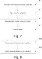
- Fig. 7 is a flowchart illustrating a method of manufacturing a switch device according to some embodiments.
- the method of Fig. 7 may be used to manufacture any of the switch devices discussed previously, and in order to avoid repetitions, will be described referring to the previous explanations. However, it is to be understood that the method of Fig. 7 may also be used to manufacture other switch devices than the ones explicitly described previously.
- the method comprises providing a crystalline semiconductor substrate, like substrates 11, 51, 61, 71 or 81 described previously.
- the method comprises forming a trench in the substrate, for example by etching, like trench 12, 52, 62, 72 or 82 described previously.
- the method comprises providing a phase change material in the trench, for example phase change material 15, 55, 65, 75 or 85 described previously.
- the phase change material may be provided partially in the trench, as also explained. For example at least 50 %, at least 60 %, at least 70 % or at least 80 % of the phase change material 75 may be provided in the trench.
- the method comprises providing a heater, which also may be provided fully or partially within the trench, for example heater 16, 56, 66, 76 or 86 described previously.
- FIG. 7 may include contacting the phase change material or the heater, for example as shown and described with reference to Figs. 5 to 8 , providing a barrier material between phase change material and the heater (e.g. barrier layer 17) between 92 and 93, providing a thermal buffer between the phase change material and the substrate, or providing filler material, as also shown and described with reference to Figs. 5 to 8 .
- a barrier material between phase change material and the heater e.g. barrier layer 17
- FIG. 7 may include contacting the phase change material or the heater, for example as shown and described with reference to Figs. 5 to 8 , providing a barrier material between phase change material and the heater (e.g. barrier layer 17) between 92 and 93, providing a thermal buffer between the phase change material and the substrate, or providing filler material, as also shown and described with reference to Figs. 5 to 8 .
- Fig. 8 illustrates a method of operating a switch device, wherein the switch device is implemented using a trench in a crystalline semiconductor substrate as describe previously. Acts or events described with respect to Fig. 8 may be performed in different order and may be performed repeatedly to turn the switch on and off.
- the method comprises providing power to the heater to turn the switch on.
- the power is provided in a manner to perform the already described set operation, i.e. heat the phase change material to a temperature above the crystallization temperature and below the melt temperature.
- the method comprises providing power to the heater to turn the switch off, i.e. here the power is provided in a manner as described for the reset operation above, that the temperature of the phase change material is raised above the melt temperature (for example above about 700°C) followed by a fast cooling (for example larger than 10 10 K/s) to turn the phase change material into an amorphous phase state.
- Pulse length of power provided to the heater at 1000 or 1001 may be of the order of 1 ⁇ s or below.
- an increased cooling rate or a reduction of the energy needed for switching the switch up to 50 % depending on the exact geometry used, may be obtained in some implementations.
Landscapes
- Engineering & Computer Science (AREA)
- Manufacturing & Machinery (AREA)
- Semiconductor Integrated Circuits (AREA)
- Semiconductor Memories (AREA)
- Micromachines (AREA)
Abstract
Description
- The present application relates to switch devices and methods for manufacturing and operating such switch devices.
- The technical requirements for radio frequency applications (RF applications) using high frequencies, such as radar sensing and mobile communication according to the 5G standard, are increasing. In particular, switches having improved characteristics compared to state of the art CMOS switches will be required to meet future demands. Phase change switches are considered as promising candidates for switching RF signals. Such phase change switches use a phase change material (PCM) which typically exhibits a higher electric conductivity in a crystalline phase state than in an amorphous phase state. By changing the phase state of the phase change material, a switching device including such a material may be switched on or off.
- For example, to change the phase state from amorphous to crystalline, typically a heater is employed heating the phase change material causing crystallization. This switching on is also referred to as a set operation of the switching device. In this set operation, the heater is actuated in such a way that the temperature of the phase change material is above its crystallization temperature, typically about 350°C, but below the melt temperature of typically in a range of 600°C to 900°C, for example. The length of the heating pulse caused by the heater is chosen such that any amorphous region present in the PCM can regrow into the crystalline phase state.
- When switching off the switching device, also referred to as reset operation, the heater is actuated in such a way that the temperature of the PCM is raised above the melt temperature (e.g. above about 600°C to 900°C), followed by rapid cooldown which freezes the phase change material into an amorphous state.
- Heating the phase change material causes energy losses when also other adjacent components and structures are heated. Furthermore, for the rapid cooldown, a corresponding thermal coupling to a heat sink is required.
- A switching device as defined in claim 1 and a method as defined in claim 14 are provided. The dependent claims define further embodiments.
- According to an embodiment, a switch device is provided, comprising:
- a substrate,
- a trench formed in the substrate,
- a phase change material disposed at least partially in the trench, and
- a heater configured to heat the phase change material.
- According to another embodiment, a method for manufacturing a switch device is provided, comprising:
- providing a substrate,
- forming a trench in the crystalline semiconductor substrate,
- providing a phase change material in the trench, and
- providing a heater configured to heat the phase change material.
- The above summary is merely intended to give a brief overview over some aspects of some embodiments and is not to be construed as limiting in any way.
-
-
Fig. 1 is a cross-sectional view of a switch device according to an embodiment. -
Fig. 2 is a cross-sectional view of a switch device according to a comparative example. -
Fig. 3 , consisting ofFigs. 3A to 3C , illustrates a switch device according to an embodiment, whereinFig. 3A is a schematic top view,Fig. 3B is a schematic cross-sectional view along aline 511 inFig. 3A , andFig. 3C is a schematic cross-sectional view along aline 512 inFig. 3A . -
Fig. 4 , consisting ofFigs. 4A to 4C , illustrates a switch device according to an embodiment, whereinFig. 4A is a schematic top view,Fig. 4B is a schematic cross-sectional view along aline 611 inFig. 4A , andFig. 4C is a schematic cross-sectional view along aline 612 inFig. 4A . -
Fig. 5 , consisting ofFigs. 5A to 5C , illustrates a switch device according to an embodiment, whereinFig. 5A is a schematic top view,Fig. 5B is a schematic cross-sectional view along aline 711 inFig. 5A , andFig. 5C is a schematic cross-sectional view along aline 712 inFig. 5A . -
Fig. 6 , consisting ofFigs. 6A to 6C , illustrates a switch device according to an embodiment, whereinFig. 6A is a schematic top view,Fig. 6B is a schematic cross-sectional view along aline 811 inFig. 6A , andFig. 6C is a schematic cross-sectional view along aline 812 inFig. 6A . -
Fig. 7 is a flowchart illustrating a method for manufacturing a switch device according to some embodiments. -
Fig. 8 is a flowchart illustrating a method for operating a switch device according to some embodiments. - In the following, various embodiments will be described in detail referring to the attached drawings. The embodiments described hereinafter are to be taken as examples only and are not to be construed as limiting. For example, while in embodiments specific shapes and arrangements of components of a switch device like a phase change material or a heater are shown, in other embodiments other configurations may be used. For example, while in some embodiments a heater is provided above a phase change material, in other embodiments a heater may be provided below a phase change material.
- Besides the features (for example components, elements, acts, events or the like) explicitly shown and described, in other embodiments additional features may be provided, for example features as used in conventional switch devices using phase change materials. For example, embodiments herein relate to switch devices where a phase change material is arranged at least partially within a trench formed in a substrate. Other components, like control circuitry for controlling a heater, radio frequency (RF) circuitry using the switch device and the like may be implemented in a conventional manner. Such additional components may be integrated with the described switch devices on the same substrate, but may also be provided separately for example on one or more separate chip dies, which in some implementations then may be combined with the switch device in a common package.
- Functionally similar components in various figures bear the same references numerals, with the first digit corresponding to the number of the figure. Just to give an example, a heater is designated with
reference numeral 16 inFig. 1 , withreference numeral 26 inFig. 2 , withreference numeral 56 inFig. 3 etc. - Therefore, these elements will not be described in detail repeatedly, but general explanations will be made when these elements occur for the first time (e.g. referring to
Fig. 1 ), and for following Figures only differences to the previously described Figures will be described in detail. For example, materials for different components like heaters and phase change materials will be explained with reference toFig. 1 and apply likewise to corresponding components of other embodiments. - Turning now to the figures,
Fig. 1 . is a cross-sectional view of a switch device according to an embodiment. -
Switch device 10 ofFig. 1 comprises acrystalline semiconductor substrate 11.Crystalline semiconductor substrate 11 as used herein means that the part ofsubstrate 11 where the device shown is provided is made of a crystalline semiconductor material, for example silicon, gallium arsenide or silicon carbide. For example,crystalline semiconductor substrate 11 may be a semiconductor wafer like a silicon wafer. In other embodiments,semiconductor substrate 11 may include a crystalline semiconductor wafer with one or more crystalline semiconductor layers grown epitaxially thereon, for example a silicon semiconductor wafer with silicon layers epitaxially grown thereon (doped or undoped). In yet other embodiments,crystalline semiconductor substrate 11 may be an active layer of a semiconductor wafer having an insulation layer incorporated therein like an active wafer layer of a silicon-on-insulator (SOI) wafer. The active layer of such a wafer is the layer on which for example semiconductor devices are formed. Also such a substrate may further include crystalline epitaxial semiconductor layers formed on the layer. While a crystalline semiconductor substrate will be used as an example herein, in other embodiments other substrates, for example non-semiconductor crystalline substrates may be used, for example sapphire substrates. The term substrate, like crystalline (semiconductor) substrate, as used herein, does not include non-crystalline layers formed on a substrate like a semiconductor wafer, like dielectric layers, and also does not include metal layers. Such dielectric layers or metal layers may for example be formed in so-called back end of line (BEOL) processing.Crystalline semiconductor substrate 11 will be referred to simply as substrate in the following. The same applies to substrates used in further embodiments described further below. - In
crystalline semiconductor substrate 11, atrench 12 is formed. A trench generally refers to a recess formed in the substrate. Such trenches may be formed by etching. In some embodiments, conventional techniques used for forming trenches in semiconductor substrates may be employed, for example techniques used for forming trenches used for shallow trench isolation (STI) or semiconductor devices built in trenches. In some implementations, the trench may have an elongated shape, which means that the trench is longer in a length direction than in a width direction, for example more than two times longer, more than three times longer, more than 10 times longer or even more than 100 times longer. - Compared to trenches used in conventional semiconductor devices, a ratio of the width of the trench to the depth of the trench may be comparatively large, also referred to as shallow trench. For example, an aspect ratio of width : depth (assuming that the width is smaller than the length) may be between 5:1 and 1:1, for example between 3:1 and 1.5:1, for example about 2:1. An aspect ratio of 2:1 may correspond to a cross-section in the width direction similar to a semicircle. Such shallow trenches in some implementations may lead to improved thermal properties compared to other trench geometries. However, in other implementations also deeper trenches with an aspect ratio width : depth smaller than 1:1 may be used. Such deeper trenches may reduce area requirements in some implementations. Generally, depth, length and width of the trench depend on the desired properties of the switch device. For example, for lower depth a larger width and/or length is needed to have a same area of phase change material (for example to have a same area than a specific conventional planar switch).
- In
trench 12, various elements may then be formed layer by layer. In the embodiment ofFig. 1 , first, athermal buffer layer 13 is provided, which may for example be made of silicon oxide or other dielectrical materials. Following the thermal buffer layer, a phase change material (PCM) 15 is provided. An example for a usable phase change material is Germanium Telluride. - As can be seen in
Fig. 1 , thephase change material 15 is at least partially provided withintrench 12. In some embodiments this may enhance cooling ofPCM 15 in a reset operation due to enhanced thermal coupling tosubstrate 11, which serves as a heat sink. - In some embodiments, the shape of a side of
PCM 15 facingtrench 12 in at least one cross-section (for example the one shown inFig. 1 ) matched or follows the shape oftrench 12, such thatPCM 15 is provided along the walls and bottom oftrench 12, and separated fromtrench 12 bythermal buffer layer 13. This may help to achieve a desired cooling rate, which in some embodiments may be larger than 1010K/s. As can be seen inFig. 1 , a side ofPCM 15 facingtrench 12 may have a curved portion, in this case at a bottom oftrench 12, in at least one cross-section. This curved portion may further serve to enhance cooling. Yet, in other embodiments other shapes are possible, for example angular shapes. - Furthermore, a
heater 16 is provided separated fromPCM 15 by abarrier layer 17.Barrier layer 17 may for example be made of silicon nitride. Suitable heater materials forheater 16 include polycrystalline silicon or Tungsten.Heater 16 in the embodiment ofFig. 1 is also partially provided withintrench 12. In the cross-section ofFig. 1 , furthermorePCM 15 partially surrounds heater 16 (on three sides in case ofFig. 1 ). This may lead to an increased heat transfer fromheater 16 toPCM 15 and may reduce heat dissipated to the environment, for example to adielectric material 19 which in the example ofFig. 1 is used on top ofsubstrate 11 as a filler material, for example for planarization purposes and/or as dielectric material in back end of line (BEOL) processes. Furthermore, the curved shape ofPCM 15 already discussed above together with the surrounding facingheater 16 byPCM 15 leads to a greater outer surface ofPCM 15 towardssubstrate 11 serving is a heat sink compared to a surface ofheater 16. Therefore, a thermal resistance of the heater may be higher than in a planar design, even when a corresponding thermal resistance ofPCM layer 15 is the same. This will be explained in more detail further below. Additionally, in some embodiments with this design the volume ofheater 16 may be reduced compared to conventional solutions. -
PCM 15 is coupled to contactpads heater 16 described later on, are also labeled RF1 and RF2.Contact pads PCM 15 via vertical interconnects (e.g. VIA, vertical interconnect axis) 18A, 18B respectively.Contact pads material 29 may be provided as inconventional BEOL processing in semiconductor technology. As briefly mentioned above,heater 16 may be also contacted to be able to supply electric power toheater 16. In operation of the switch device, by operatingheater 16PCM 15 may be brought to a crystalline phase state having a low-ohmic resistance or an amorphous phase state having a high-ohmic resistance, and therefore a low-ohmic connection betweencontact pads pad 14A and/or 14B. It should be noted thatcontact pads Fig. 1 , but described for other embodiments) need not be pads for external contacting, but may also be part of metal leads or wires extending to other parts of a circuit. - For better understanding of
switch device 10 ofFig. 1 , it will be compared to areference switch device 20 ofFig. 2 using a conventional planar technology.Fig. 2 shows a cross-sectional view ofswitch device 20 which corresponds to the cross-sectional view ofFig. 1 . In contrast to the embodiment ofFig. 1 , in asubstrate 21 no trench is provided, but aPCM 25 is provided onsubstrate 21 separated by athermal buffer layer 23 in a planar manner. Aheater 26 is provided onPCM 25 separated by abarrier layer 27 also in a planar manner.PCM 25 is contacted viacontact pads vertical interconnects dielectric material 29 is used for planarization and isolation. - As can be seen in
Fig. 2 , whenheating PCM 25, alsofiller material 29 has to be heated. Furthermore continuous thermal losses occur due to thermal losses viafiller material 29.. Furthermore, cooling withsubstrate 21 as a heatsink may be comparatively slow. As mentioned initially, cooling with a high cooling rate is required to bring the PCM to an amorphous phase state. - In contrast thereto, in
Fig. 1 the placement ofPCM 15 intrench 12, and the placement ofheater 16 such that it is partially surrounded byPCM 15, essentially makes thermal losses to filler material or BEOL layers negligible, or reduces them significantly. It is to be understood that some losses may remain, but these are significantly smaller than inFig. 2 . This may reduce the power needed forheating PCM 15. - Furthermore, by the placement of
PCM 15 intrench 12, thermal contact to thesubstrate 11 may be enhanced.. This may contribute to a fast cooling ofPCM 15 when resetting the switch device, i.e. puttingPCM 15 to an amorphous phase state. - Various configurations for arranging a phase change material and a heater in a trench are possible. Some of these possible configurations will be explained now referring to
Figs. 3 to 6 . Each ofFigs. 3 to 6 includes subfigures A, B and C, i.e. 3A, 3B, 3C forFig. 3 ,4A ,4B, 4C forFig. 4 etc. Subfigures A show schematic top views on the substrate, and subfigures B and C show schematic cross-sectional views. - In
Fig. 3 ,Fig. 3A shows top view of a switch device according to an embodiment.Fig. 3B shows a schematic cross-sectional view along a dashedline 511, which is in the length direction of atrench 52. This length direction of the trench is also marked by anarrow 513.Fig. 3C shows a schematic cross-sectional view along a dashedline 512 inFig. 3A , which runs in a width direction oftrench 52. Generally, as explained previously, a length of the trench in the length direction may be larger than a width of the trench in a width direction. - In the embodiment of
Fig. 3 , the cross-sectional view ofFig. 3C in this case essentially corresponds to switchdevice 10 discussed with reference toFig. 1 . - The switch device of
Fig. 3 includes acrystalline semiconductor substrate 51,trench 52 formed insubstrate 51, athermal buffer layer 53, aphase change material 55, abarrier layer 57 and aheater 56. - In the embodiment of
Fig. 3 , the phase change material is provided in the width direction oftrench 52, and the heater is provided in the length direction oftrench 52. This means, as seen inFig. 3A and5C , thatcontact pads phase change material 52 are provided such that the signal flow throughphase change material 55 is in the width direction.Contact pads filler material 59 and coupled tophase change material 55 viavertical interconnects - For providing current to
heater 56,contact pads heater 56 byvertical contacts Fig. 3B , extend intoheater 56 to provide a more uniform current distribution. Current through heater 5A, when present, therefore flows essentially in the length direction of the trench. -
Fig. 4 illustrates a further example configuration.Fig. 4A illustrates a top view of a switch device according to a further embodiment,Fig. 4B shows a schematic cross-sectional view along a dashedline 611, which runs in a length direction of atrench 62 as indicated by anarrow 613, andFig. 4C shows a schematic cross-sectional view along aline 612 running in a width direction oftrench 62. - In the embodiment of
Fig. 3 , a depth of the trench may be about half a length of the trench. - The switch device of
Fig. 4 includes acrystalline semiconductor substrate 61,trench 62 formed insubstrate 61, athermal buffer layer 63, aphase change material 65, abarrier layer 67 and aheater 66. - In the embodiment of
Fig. 4 ,phase change material 65 is arranged in the length direction, i.e. signal flow is in the length direction, andheater 66 is arranged in the width direction, i.e. current flow throughheater 66, is in the width direction. - As can be seen in
Fig. 4A and6B ,contact pads phase change material 65 are provided such that current flows in the length direction.Contact pads change material 65 byvertical interconnects Contact pads heater 66 are arranged in the width direction, as seen inFigs. 6A and6C . As seen inFig. 4C ,filler material 69 extends into the trench to provide a U shape ofheater 66 in the cross-sectional view ofFig. 4C , to ensure that current flows through the heater essentially "along"phase shape material 65. Without this filler, material, i.e. ifheater 66 had a filled-out U shape inFig. 4C , current would mainly flow directly fromcontact pad 610A to contactpat 610B abovesubstrate 61, such that the lower part ofheater 66 would hardly be heated. -
Fig. 5 illustrates a switch device according to a further embodiment.Fig. 5A shows a top view,Fig. 5B shows a schematic cross-sectional view along a dashedline 711 running in a length direction of atrench 72 as indicated by anarrow 713, andFig. 5C shows a schematic cross-sectional view along a dashedline 712 running in a width direction oftrench 72. - The switch device of
Fig. 5 includes acrystalline semiconductor substrate 71,trench 72 formed insubstrate 71, athermal buffer layer 73, aphase change material 75, abarrier layer 77 and aheater 76. - In the embodiment of
Fig. 5 , bothphase change material 75 andheater 76 are provided in a length direction, i.e. both signal flow throughphase change material 75 and current flow throughheater 76 are in the length direction. As, best seen in the cross-sectional view ofFig. 5B ,contact pads 74A, 74B for contactingphase change material 75 andcontact pads heater 76 may be arranged in different metal layers. In other embodiments, an arrangement in a same metal layer may be used. As can be seen in the cross-sectional view ofFig. 5B ,vertical interconnects contact pads phase change material 75, andvertical interconnects contact pads heater 76, to ensure an appropriate current distribution. -
Fig. 6 shows a switch device according to a further embodiment.Fig. 6A shows a top view,Fig. 6B shows s schematic cross-sectional view along a dashedline 811 running in a length direction of atrench 82 as indicated by anarrow 814, andFig. 6C shows a schematic cross-sectional view along a dashedline 812 running in a width direction oftrench 82. - The switch device of
Fig. 6 includes acrystalline semiconductor substrate 81,trench 82 formed insubstrate 81, athermal buffer layer 83, aphase change material 85, abarrier layer 87 and aheater 86. - In the embodiment of
Fig. 6 , bothphase change material 85 andheater 86 are arranged in the width direction, i.e. signal flow throughphase change material 85 and current flow throughheater 86 is in the width direction. As can be best seen in Figs. 8A and 8C, similar to the embodiment ofFig. 5 ,contact pads phase change material 85, viavertical interconnects contacts pads 810B contacting heater 86 viavertical interconnects Fig. 4 ,filler material 89 extends into the trench to provide a U form ofheater 86 in the cross-section ofFig. 6C , similar to what was explained with reference toFig. 4C . - As can be seen from
Figs. 5 to 8 , various configurations of providing phase change material and heater in the trench and contacting them are possible. Therefore, it is evident that this disclosure is not limited to any specific configuration. -
Fig. 7 is a flowchart illustrating a method of manufacturing a switch device according to some embodiments. The method ofFig. 7 may be used to manufacture any of the switch devices discussed previously, and in order to avoid repetitions, will be described referring to the previous explanations. However, it is to be understood that the method ofFig. 7 may also be used to manufacture other switch devices than the ones explicitly described previously. - At 90, the method comprises providing a crystalline semiconductor substrate, like
substrates - At 91, the method comprises forming a trench in the substrate, for example by etching, like
trench - At 92, the method comprises providing a phase change material in the trench, for example
phase change material phase change material 75 may be provided in the trench. - At 93, the method comprises providing a heater, which also may be provided fully or partially within the trench, for
example heater - Further process parts not explicitly shown and described in
Fig. 7 may include contacting the phase change material or the heater, for example as shown and described with reference toFigs. 5 to 8 , providing a barrier material between phase change material and the heater (e.g. barrier layer 17) between 92 and 93, providing a thermal buffer between the phase change material and the substrate, or providing filler material, as also shown and described with reference toFigs. 5 to 8 . -
Fig. 8 illustrates a method of operating a switch device, wherein the switch device is implemented using a trench in a crystalline semiconductor substrate as describe previously. Acts or events described with respect toFig. 8 may be performed in different order and may be performed repeatedly to turn the switch on and off. - At 1000 the method comprises providing power to the heater to turn the switch on. In this case, the power is provided in a manner to perform the already described set operation, i.e. heat the phase change material to a temperature above the crystallization temperature and below the melt temperature.
- AT 1001, the method comprises providing power to the heater to turn the switch off, i.e. here the power is provided in a manner as described for the reset operation above, that the temperature of the phase change material is raised above the melt temperature (for example above about 700°C) followed by a fast cooling (for example larger than 1010K/s) to turn the phase change material into an amorphous phase state.
- Pulse length of power provided to the heater at 1000 or 1001 may be of the order of 1 µs or below.
- With embodiments as discussed above, an increased cooling rate or a reduction of the energy needed for switching the switch up to 50 % depending on the exact geometry used, may be obtained in some implementations.
- Example 1. A switch device, comprising:
- a substrate,
- a trench formed in the substrate,
- a phase change material disposed at least partially in the trench, and
- a heater configured to heat the phase change material.
- Example 2. The switch device of example 1, wherein the substrate is a crystalline semiconductor substrate.
- Example 3. The switch device of example 1 or 2, wherein the heater is at least partially disposed in the trench.
- Example 4. The switch device of any one of examples 1 to 3, wherein in at least one cross-section of the switch device, a form of a side of the phase change material facing the trench follows the shape of the trench.
- Example 5. The switch device of any one of examples 1 to 4, wherein in at least one cross-section of the switch device, a side of the phase change material facing the trench has a curved portion.
- Example 6. The switch device of example 4 or 5, wherein the at least one cross-section comprises a cross-section in a width direction, wherein the width direction of the trench has a width smaller than a length of the trench in a length direction.
- Example 7. The switch device of any of examples 1 to 6, wherein the trench has a width, a length and a depth, wherein the width is smaller than the length and an aspect ratio width: depth is between 5:1 and 1:1.
- Example 8. The switch device of any one of examples 1 to 7, wherein the phase change material surrounds the heater on at least two sides of the heater in at least one cross-section of the switch device.
The at least one cross-section in the preceding examples (e.g. examples 4, 5, 8) may be the same cross-section in all examples (e.g. a cross-section in the width direction as specified in example 5), but may also refer to different corss-sections in different examples (e.g. a cross-section in width direction in one example and a cross-section in length direction in another example). - Example 9. The switch device of any one of examples 1 to 8, further comprises a thermal buffer layer arranged between the phase change material and the trench.
- Example 10. The switch device of any one of examples 1 to 9, wherein the switch device further comprises a barrier layer provided between the phase change material and the heater.
- Example 11. The switch device of any one of examples 1 to 10, wherein the trench has a length direction having a length, a width direction having a width smaller than the length and a depth direction,
wherein the device further comprises first contact pads configured to contact the phase change material, and second contact pads arranged to contact the heater. - Example 12. The switch device of example 11, wherein the first contact pads are arranged to provide signal flow through the phase change material in one of the length direction or the width direction, and the second contact pads are configured to provide current flow through the heater in the other one of the length direction or the width direction.
- Example 13. The switch device of example 11, wherein the first contact pads are arranged to provide signal flow through the phase change material in one of the length direction or the width direction, and the second contact pads are arranged to provide current flow through the heater in the one of the length direction or the width direction.
- Example 14. The switch device of any one of examples 11 to 13, wherein first vertical interconnects extend from the first contact pads to a part of the phase change material disposed in the trench.
- Example 15. The switch device of any of examples 11 to 14, wherein second vertical interconnects extend from the second contact pads into a part of the heater disposed in the trench.
- Example 16. A method for manufacturing a switch device, comprising:
- providing a substrate,
- forming a trench in the substrate,
- providing a phase change material in the trench, and
- providing a heater configured to heat the phase change material.
- Example 17. The method of example 16, wherein the method is configured to manufacture the switch device of any one of examples 1 to 15.
- Although specific embodiments have been illustrated and described herein, it will be appreciated by those of ordinary skill in the art that a variety of alternate and/or equivalent implementations may be substituted for the specific embodiments shown and described without departing from the scope of the present invention. This application is intended to cover any adaptations or variations of the specific embodiments discussed herein. Therefore, it is intended that this invention be limited only by the claims and the equivalents thereof.
Claims (15)
- A switch device (10), comprising:a substrate(11; 51; 61; 71; 81),a trench (12; 52; 62; 72; 82) formed in the substrate (11; 51; 61; 71; 81),a phase change material (15; 55; 65; 75; 85) disposed at least partially in the trench (12; 52; 62; 72; 82), anda heater (16; 56; 66; 76; 86) configured to heat the phase change material (15; 55; 65; 75; 85).
- The switch device (10) of claim 1, wherein the heater (16; 56; 66; 76; 86) is at least partially disposed in the trench (12; 52; 62; 72; 82).
- The switch device (10) of claim 1 or 2, wherein in at least one cross-section of the switch device (10), a form of a side of the phase change material (15; 55; 65; 75; 85) facing the trench (12; 52; 62; 72; 82)follows the shape of the trench(12; 52; 62; 72; 82).
- The switch device (10) of any one of claims 1 to 3, wherein in at least one cross-section of the switch device (10), a side of the phase change material (15; 55; 65; 75; 85) facing the trench (12; 52; 62; 72; 82) has a curved portion.
- The switch device (10) of any of claims 1 to 4, wherein the trench has a width, a length and a depth, wherein the width is smaller than the length and an aspect ratio width: depth is between 5:1 and 1:1.
- The switch device (10) of any one of claims 1 to 5, wherein the phase change material (15; 55; 65; 75; 85) surrounds the heater (16; 56; 66; 76; 86) on at least two sides of the heater (16; 56; 66; 76; 86) in at least one cross-section of the switch device (10).
- The switch device (10) of any one of claims 1 to 6, further comprises a thermal buffer layer (13; 53; 63; 73; 83) arranged between the phase change material (15; 55; 65; 75; 85) and the trench (12; 52; 62; 72; 82).
- The switch device (10) of any one of claims 1 to 7, wherein the switch device further comprises a barrier layer (17; 57; 67; 77; 87) provided between the phase change material (15; 55; 65; 75; 85) and the heater (16; 56; 66; 76; 86) .
- The switch device (10) of any one of claims 1 to 8, wherein the trench (12; 52; 62; 72; 82) has a length direction having a length, a width direction having a width smaller than the length and a depth direction,
wherein the device further comprises first contact pads (14A, 14B; 54A, 54B; 64A, 64B; 74A, 74B; 84A, 84B) configured to contact the phase change material (15; 55; 65; 75; 85), and second contact pads (510A, 510B; 610A, 610B; 710A, 710B; 810A, 810B) arranged to contact the heater (16; 56; 66; 76; 86) . - The switch device (10) of claim 9, wherein the first contact pads (14A, 14B; 54A, 54B; 64A, 64B; 74A, 74B; 84A, 84B) are arranged to provide signal flow through the phase change material (15; 55; 65; 75; 85) in one of the length direction or the width direction, and the second contact pads (510A, 510B; 610A, 610B; 710A, 710B; 810A, 810B) are configured to provide current flow through the heater (16; 56; 66; 76; 86) in the other one of the length direction or the width direction.
- The switch device (10) of claim 9, wherein the first contact pads (14A, 14B; 54A, 54B; 64A, 64B; 74A, 74B; 84A, 84B) are arranged to provide signal flow through the phase change material (15; 55; 65; 75; 85) in one of the length direction or the width direction, and the second contact pads (510A, 510B; 610A, 610B; 710A, 710B; 810A, 810B) are arranged to provide current flow through the heater (16; 56; 66; 76; 86) in the one of the length direction or the width direction.
- The switch device (10) of any one of claim 9 to 11, wherein first vertical interconnects (68A, 68B; 78A, 78B) extend from the first contact pads (14A, 14B; 54A, 54B; 64A, 64B; 74A, 74B; 84A, 84B) to a part of the phase change material (15; 55; 65; 75; 85) disposed in the trench (12; 52; 62; 72; 82).
- The switch device (10) of any of claims 9 to 12, wherein second vertical interconnects (514A, 514B; 714A, 714B) extend from the second contact pads (510A, 510B; 610A, 610B; 710A, 710B; 810A, 810B) into a part of the heater (16; 56; 66; 76; 86) disposed in the trench (12; 52; 62; 72; 82).
- A method for manufacturing a switch device (10), comprising:providing (90) a substrate (11; 51; 61; 71; 81),forming (91) a trench (12; 52; 62; 72; 82) in the substrate (11; 51; 61; 71; 81),providing (92) a phase change material (15; 55; 65; 75; 85) in the trench (12; 52; 62; 72; 82), andproviding (93) a heater (16; 56; 66; 76; 86) configured to heat the phase change material (15; 55; 65; 75; 85).
- The method of claim 14, wherein the method is configured to manufacture the switch device (10) of any one of claims 1 to 13.
Priority Applications (2)
| Application Number | Priority Date | Filing Date | Title |
|---|---|---|---|
| EP20176725.8A EP3916818B1 (en) | 2020-05-27 | 2020-05-27 | Switch device with u-shaped phase change material and method for manufacturing the same |
| US17/330,610 US11963466B2 (en) | 2020-05-27 | 2021-05-26 | Switch device and method for manufacturing a switch device |
Applications Claiming Priority (1)
| Application Number | Priority Date | Filing Date | Title |
|---|---|---|---|
| EP20176725.8A EP3916818B1 (en) | 2020-05-27 | 2020-05-27 | Switch device with u-shaped phase change material and method for manufacturing the same |
Publications (2)
| Publication Number | Publication Date |
|---|---|
| EP3916818A1 true EP3916818A1 (en) | 2021-12-01 |
| EP3916818B1 EP3916818B1 (en) | 2024-10-09 |
Family
ID=70861267
Family Applications (1)
| Application Number | Title | Priority Date | Filing Date |
|---|---|---|---|
| EP20176725.8A Active EP3916818B1 (en) | 2020-05-27 | 2020-05-27 | Switch device with u-shaped phase change material and method for manufacturing the same |
Country Status (2)
| Country | Link |
|---|---|
| US (1) | US11963466B2 (en) |
| EP (1) | EP3916818B1 (en) |
Families Citing this family (1)
| Publication number | Priority date | Publication date | Assignee | Title |
|---|---|---|---|---|
| US11711989B2 (en) * | 2021-03-23 | 2023-07-25 | International Business Machines Corporation | Phase change memory |
Citations (4)
| Publication number | Priority date | Publication date | Assignee | Title |
|---|---|---|---|---|
| US20080029753A1 (en) * | 2006-08-01 | 2008-02-07 | Yang Xu | Configurable circuits using phase change switches |
| WO2009001262A1 (en) * | 2007-06-28 | 2008-12-31 | Nxp B.V. | Electric device comprising phase change material and heating element |
| WO2009130668A1 (en) * | 2008-04-21 | 2009-10-29 | Nxp B.V. | Phase-change-material memory with multibit memory cells and method for fabricating the same |
| US20140264230A1 (en) * | 2013-03-14 | 2014-09-18 | Northrop Grumman Systems Corporation | Phase change material switch and method of making the same |
Family Cites Families (3)
| Publication number | Priority date | Publication date | Assignee | Title |
|---|---|---|---|---|
| US6815704B1 (en) * | 2003-09-04 | 2004-11-09 | Silicon Storage Technology, Inc. | Phase change memory device employing thermally insulating voids |
| US7800092B2 (en) * | 2006-08-15 | 2010-09-21 | Micron Technology, Inc. | Phase change memory elements using energy conversion layers, memory arrays and systems including same, and methods of making and using |
| US9117748B2 (en) * | 2013-01-31 | 2015-08-25 | Infineon Technologies Ag | Semiconductor device including a phase change material |
-
2020
- 2020-05-27 EP EP20176725.8A patent/EP3916818B1/en active Active
-
2021
- 2021-05-26 US US17/330,610 patent/US11963466B2/en active Active
Patent Citations (4)
| Publication number | Priority date | Publication date | Assignee | Title |
|---|---|---|---|---|
| US20080029753A1 (en) * | 2006-08-01 | 2008-02-07 | Yang Xu | Configurable circuits using phase change switches |
| WO2009001262A1 (en) * | 2007-06-28 | 2008-12-31 | Nxp B.V. | Electric device comprising phase change material and heating element |
| WO2009130668A1 (en) * | 2008-04-21 | 2009-10-29 | Nxp B.V. | Phase-change-material memory with multibit memory cells and method for fabricating the same |
| US20140264230A1 (en) * | 2013-03-14 | 2014-09-18 | Northrop Grumman Systems Corporation | Phase change material switch and method of making the same |
Non-Patent Citations (1)
| Title |
|---|
| YOUNG R M ET AL: "Improvements in GeTe-based Phase Change RF Switches", 2018 IEEE/MTT-S INTERNATIONAL MICROWAVE SYMPOSIUM, 10-15 JUNE 2018, PHILADELPHIA, PA, 2018, pages 832 - 835, XP033387924, DOI: 10.1109/MWSYM.2018.8439212 * |
Also Published As
| Publication number | Publication date |
|---|---|
| US11963466B2 (en) | 2024-04-16 |
| EP3916818B1 (en) | 2024-10-09 |
| US20210376234A1 (en) | 2021-12-02 |
Similar Documents
| Publication | Publication Date | Title |
|---|---|---|
| US10079230B2 (en) | Double-sided vertical semiconductor device with thinned substrate | |
| KR101758852B1 (en) | Semiconductor-on-insulator with backside heat dissipation | |
| US8466054B2 (en) | Thermal conduction paths for semiconductor structures | |
| US20220285550A1 (en) | Semiconductor Device Having Contact Trenches Extending from Opposite Sides of a Semiconductor Body | |
| TWI618248B (en) | Vertical semiconductor component with thin substrate | |
| JP5122762B2 (en) | Power semiconductor device, manufacturing method thereof, and driving method thereof | |
| US7541644B2 (en) | Semiconductor device with effective heat-radiation | |
| TWI603444B (en) | Insulator-on-insulator integrated circuit with interconnects under insulator | |
| CN110313066A (en) | Integrated circuit connection arrangement for minimizing crosstalk | |
| JP2012511257A (en) | RF apparatus and method featuring grooves under bond pads | |
| US20240040803A1 (en) | Integrated circuit, method for manufacturing an integrated circuit, wafer and method for manufacturing a wafer | |
| JP2016058466A (en) | Silicon carbide semiconductor device | |
| US10784179B2 (en) | Semiconductor device and method for fabricating the same | |
| JP2021082753A (en) | Semiconductor device and manufacturing method therefor | |
| JP3791459B2 (en) | Semiconductor device and manufacturing method thereof | |
| EP3916818B1 (en) | Switch device with u-shaped phase change material and method for manufacturing the same | |
| CN110943056A (en) | High-resistance chip with heat dissipation structure and manufacturing method thereof | |
| JP2006303145A (en) | Semiconductor device | |
| US6432809B1 (en) | Method for improved passive thermal flow in silicon on insulator devices | |
| CN119968109A (en) | Phase change switch with adhesive layer | |
| CN113421913B (en) | A kind of SOI chip, preparation method, intelligent power module, electric appliance and air conditioner | |
| JP2006108663A (en) | Vertically conductive power electronic device and method for realizing the same | |
| KR20190008464A (en) | Semiconductor Device with Stacking Structure of Silicon-Conductor layer-Silicon | |
| JP2023069720A (en) | Semiconductor device | |
| US12575338B2 (en) | Phase change switch fabricated with front end of the line process |
Legal Events
| Date | Code | Title | Description |
|---|---|---|---|
| PUAI | Public reference made under article 153(3) epc to a published international application that has entered the european phase |
Free format text: ORIGINAL CODE: 0009012 |
|
| STAA | Information on the status of an ep patent application or granted ep patent |
Free format text: STATUS: THE APPLICATION HAS BEEN PUBLISHED |
|
| AK | Designated contracting states |
Kind code of ref document: A1 Designated state(s): AL AT BE BG CH CY CZ DE DK EE ES FI FR GB GR HR HU IE IS IT LI LT LU LV MC MK MT NL NO PL PT RO RS SE SI SK SM TR |
|
| B565 | Issuance of search results under rule 164(2) epc |
Effective date: 20201103 |
|
| STAA | Information on the status of an ep patent application or granted ep patent |
Free format text: STATUS: REQUEST FOR EXAMINATION WAS MADE |
|
| 17P | Request for examination filed |
Effective date: 20220525 |
|
| RBV | Designated contracting states (corrected) |
Designated state(s): AL AT BE BG CH CY CZ DE DK EE ES FI FR GB GR HR HU IE IS IT LI LT LU LV MC MK MT NL NO PL PT RO RS SE SI SK SM TR |
|
| REG | Reference to a national code |
Ref country code: DE Ref legal event code: R079 Free format text: PREVIOUS MAIN CLASS: H01L0045000000 Ipc: H10N0070200000 Ref country code: DE Ref legal event code: R079 Ref document number: 602020038919 Country of ref document: DE Free format text: PREVIOUS MAIN CLASS: H01L0045000000 Ipc: H10N0070200000 |
|
| GRAP | Despatch of communication of intention to grant a patent |
Free format text: ORIGINAL CODE: EPIDOSNIGR1 |
|
| STAA | Information on the status of an ep patent application or granted ep patent |
Free format text: STATUS: GRANT OF PATENT IS INTENDED |
|
| RIC1 | Information provided on ipc code assigned before grant |
Ipc: H10N 70/20 20230101AFI20240605BHEP |
|
| INTG | Intention to grant announced |
Effective date: 20240620 |
|
| GRAS | Grant fee paid |
Free format text: ORIGINAL CODE: EPIDOSNIGR3 |
|
| GRAA | (expected) grant |
Free format text: ORIGINAL CODE: 0009210 |
|
| STAA | Information on the status of an ep patent application or granted ep patent |
Free format text: STATUS: THE PATENT HAS BEEN GRANTED |
|
| AK | Designated contracting states |
Kind code of ref document: B1 Designated state(s): AL AT BE BG CH CY CZ DE DK EE ES FI FR GB GR HR HU IE IS IT LI LT LU LV MC MK MT NL NO PL PT RO RS SE SI SK SM TR |
|
| REG | Reference to a national code |
Ref country code: CH Ref legal event code: EP |
|
| P01 | Opt-out of the competence of the unified patent court (upc) registered |
Free format text: CASE NUMBER: APP_51418/2024 Effective date: 20240911 |
|
| REG | Reference to a national code |
Ref country code: DE Ref legal event code: R096 Ref document number: 602020038919 Country of ref document: DE |
|
| REG | Reference to a national code |
Ref country code: IE Ref legal event code: FG4D |
|
| REG | Reference to a national code |
Ref country code: LT Ref legal event code: MG9D |
|
| REG | Reference to a national code |
Ref country code: NL Ref legal event code: MP Effective date: 20241009 |
|
| REG | Reference to a national code |
Ref country code: AT Ref legal event code: MK05 Ref document number: 1732097 Country of ref document: AT Kind code of ref document: T Effective date: 20241009 |
|
| PG25 | Lapsed in a contracting state [announced via postgrant information from national office to epo] |
Ref country code: NL Free format text: LAPSE BECAUSE OF FAILURE TO SUBMIT A TRANSLATION OF THE DESCRIPTION OR TO PAY THE FEE WITHIN THE PRESCRIBED TIME-LIMIT Effective date: 20241009 |
|
| PG25 | Lapsed in a contracting state [announced via postgrant information from national office to epo] |
Ref country code: NL Free format text: LAPSE BECAUSE OF FAILURE TO SUBMIT A TRANSLATION OF THE DESCRIPTION OR TO PAY THE FEE WITHIN THE PRESCRIBED TIME-LIMIT Effective date: 20241009 |
|
| PG25 | Lapsed in a contracting state [announced via postgrant information from national office to epo] |
Ref country code: IS Free format text: LAPSE BECAUSE OF FAILURE TO SUBMIT A TRANSLATION OF THE DESCRIPTION OR TO PAY THE FEE WITHIN THE PRESCRIBED TIME-LIMIT Effective date: 20250209 Ref country code: HR Free format text: LAPSE BECAUSE OF FAILURE TO SUBMIT A TRANSLATION OF THE DESCRIPTION OR TO PAY THE FEE WITHIN THE PRESCRIBED TIME-LIMIT Effective date: 20241009 Ref country code: PT Free format text: LAPSE BECAUSE OF FAILURE TO SUBMIT A TRANSLATION OF THE DESCRIPTION OR TO PAY THE FEE WITHIN THE PRESCRIBED TIME-LIMIT Effective date: 20250210 |
|
| PG25 | Lapsed in a contracting state [announced via postgrant information from national office to epo] |
Ref country code: FI Free format text: LAPSE BECAUSE OF FAILURE TO SUBMIT A TRANSLATION OF THE DESCRIPTION OR TO PAY THE FEE WITHIN THE PRESCRIBED TIME-LIMIT Effective date: 20241009 |
|
| PG25 | Lapsed in a contracting state [announced via postgrant information from national office to epo] |
Ref country code: BG Free format text: LAPSE BECAUSE OF FAILURE TO SUBMIT A TRANSLATION OF THE DESCRIPTION OR TO PAY THE FEE WITHIN THE PRESCRIBED TIME-LIMIT Effective date: 20241009 |
|
| PG25 | Lapsed in a contracting state [announced via postgrant information from national office to epo] |
Ref country code: ES Free format text: LAPSE BECAUSE OF FAILURE TO SUBMIT A TRANSLATION OF THE DESCRIPTION OR TO PAY THE FEE WITHIN THE PRESCRIBED TIME-LIMIT Effective date: 20241009 |
|
| PG25 | Lapsed in a contracting state [announced via postgrant information from national office to epo] |
Ref country code: NO Free format text: LAPSE BECAUSE OF FAILURE TO SUBMIT A TRANSLATION OF THE DESCRIPTION OR TO PAY THE FEE WITHIN THE PRESCRIBED TIME-LIMIT Effective date: 20250109 |
|
| PG25 | Lapsed in a contracting state [announced via postgrant information from national office to epo] |
Ref country code: GR Free format text: LAPSE BECAUSE OF FAILURE TO SUBMIT A TRANSLATION OF THE DESCRIPTION OR TO PAY THE FEE WITHIN THE PRESCRIBED TIME-LIMIT Effective date: 20250110 Ref country code: LV Free format text: LAPSE BECAUSE OF FAILURE TO SUBMIT A TRANSLATION OF THE DESCRIPTION OR TO PAY THE FEE WITHIN THE PRESCRIBED TIME-LIMIT Effective date: 20241009 Ref country code: AT Free format text: LAPSE BECAUSE OF FAILURE TO SUBMIT A TRANSLATION OF THE DESCRIPTION OR TO PAY THE FEE WITHIN THE PRESCRIBED TIME-LIMIT Effective date: 20241009 |
|
| PG25 | Lapsed in a contracting state [announced via postgrant information from national office to epo] |
Ref country code: PL Free format text: LAPSE BECAUSE OF FAILURE TO SUBMIT A TRANSLATION OF THE DESCRIPTION OR TO PAY THE FEE WITHIN THE PRESCRIBED TIME-LIMIT Effective date: 20241009 |
|
| PG25 | Lapsed in a contracting state [announced via postgrant information from national office to epo] |
Ref country code: RS Free format text: LAPSE BECAUSE OF FAILURE TO SUBMIT A TRANSLATION OF THE DESCRIPTION OR TO PAY THE FEE WITHIN THE PRESCRIBED TIME-LIMIT Effective date: 20250109 |
|
| PG25 | Lapsed in a contracting state [announced via postgrant information from national office to epo] |
Ref country code: SM Free format text: LAPSE BECAUSE OF FAILURE TO SUBMIT A TRANSLATION OF THE DESCRIPTION OR TO PAY THE FEE WITHIN THE PRESCRIBED TIME-LIMIT Effective date: 20241009 |
|
| PG25 | Lapsed in a contracting state [announced via postgrant information from national office to epo] |
Ref country code: DK Free format text: LAPSE BECAUSE OF FAILURE TO SUBMIT A TRANSLATION OF THE DESCRIPTION OR TO PAY THE FEE WITHIN THE PRESCRIBED TIME-LIMIT Effective date: 20241009 |
|
| REG | Reference to a national code |
Ref country code: DE Ref legal event code: R097 Ref document number: 602020038919 Country of ref document: DE |
|
| PG25 | Lapsed in a contracting state [announced via postgrant information from national office to epo] |
Ref country code: EE Free format text: LAPSE BECAUSE OF FAILURE TO SUBMIT A TRANSLATION OF THE DESCRIPTION OR TO PAY THE FEE WITHIN THE PRESCRIBED TIME-LIMIT Effective date: 20241009 |
|
| PG25 | Lapsed in a contracting state [announced via postgrant information from national office to epo] |
Ref country code: RO Free format text: LAPSE BECAUSE OF FAILURE TO SUBMIT A TRANSLATION OF THE DESCRIPTION OR TO PAY THE FEE WITHIN THE PRESCRIBED TIME-LIMIT Effective date: 20241009 |
|
| PG25 | Lapsed in a contracting state [announced via postgrant information from national office to epo] |
Ref country code: SK Free format text: LAPSE BECAUSE OF FAILURE TO SUBMIT A TRANSLATION OF THE DESCRIPTION OR TO PAY THE FEE WITHIN THE PRESCRIBED TIME-LIMIT Effective date: 20241009 |
|
| PG25 | Lapsed in a contracting state [announced via postgrant information from national office to epo] |
Ref country code: CZ Free format text: LAPSE BECAUSE OF FAILURE TO SUBMIT A TRANSLATION OF THE DESCRIPTION OR TO PAY THE FEE WITHIN THE PRESCRIBED TIME-LIMIT Effective date: 20241009 |
|
| PG25 | Lapsed in a contracting state [announced via postgrant information from national office to epo] |
Ref country code: IT Free format text: LAPSE BECAUSE OF FAILURE TO SUBMIT A TRANSLATION OF THE DESCRIPTION OR TO PAY THE FEE WITHIN THE PRESCRIBED TIME-LIMIT Effective date: 20241009 |
|
| PLBE | No opposition filed within time limit |
Free format text: ORIGINAL CODE: 0009261 |
|
| STAA | Information on the status of an ep patent application or granted ep patent |
Free format text: STATUS: NO OPPOSITION FILED WITHIN TIME LIMIT |
|
| PG25 | Lapsed in a contracting state [announced via postgrant information from national office to epo] |
Ref country code: SE Free format text: LAPSE BECAUSE OF FAILURE TO SUBMIT A TRANSLATION OF THE DESCRIPTION OR TO PAY THE FEE WITHIN THE PRESCRIBED TIME-LIMIT Effective date: 20241009 |
|
| 26N | No opposition filed |
Effective date: 20250710 |
|
| PGFP | Annual fee paid to national office [announced via postgrant information from national office to epo] |
Ref country code: DE Payment date: 20250721 Year of fee payment: 6 |
|
| REG | Reference to a national code |
Ref country code: CH Ref legal event code: H13 Free format text: ST27 STATUS EVENT CODE: U-0-0-H10-H13 (AS PROVIDED BY THE NATIONAL OFFICE) Effective date: 20251223 |
|
| PG25 | Lapsed in a contracting state [announced via postgrant information from national office to epo] |
Ref country code: LU Free format text: LAPSE BECAUSE OF NON-PAYMENT OF DUE FEES Effective date: 20250527 |
|
| PG25 | Lapsed in a contracting state [announced via postgrant information from national office to epo] |
Ref country code: CH Free format text: LAPSE BECAUSE OF NON-PAYMENT OF DUE FEES Effective date: 20250531 |
|
| GBPC | Gb: european patent ceased through non-payment of renewal fee |
Effective date: 20250527 |
|
| REG | Reference to a national code |
Ref country code: BE Ref legal event code: MM Effective date: 20250531 |
|
| PG25 | Lapsed in a contracting state [announced via postgrant information from national office to epo] |
Ref country code: MC Free format text: LAPSE BECAUSE OF FAILURE TO SUBMIT A TRANSLATION OF THE DESCRIPTION OR TO PAY THE FEE WITHIN THE PRESCRIBED TIME-LIMIT Effective date: 20241009 |
|
| PG25 | Lapsed in a contracting state [announced via postgrant information from national office to epo] |
Ref country code: GB Free format text: LAPSE BECAUSE OF NON-PAYMENT OF DUE FEES Effective date: 20250527 |
|
| PG25 | Lapsed in a contracting state [announced via postgrant information from national office to epo] |
Ref country code: IE Free format text: LAPSE BECAUSE OF NON-PAYMENT OF DUE FEES Effective date: 20250527 |
|
| PG25 | Lapsed in a contracting state [announced via postgrant information from national office to epo] |
Ref country code: BE Free format text: LAPSE BECAUSE OF NON-PAYMENT OF DUE FEES Effective date: 20250531 |
|
| PG25 | Lapsed in a contracting state [announced via postgrant information from national office to epo] |
Ref country code: FR Free format text: LAPSE BECAUSE OF NON-PAYMENT OF DUE FEES Effective date: 20250531 |