EP3916777A1 - Impinging jet manifold for chip cooling near edge jets - Google Patents
Impinging jet manifold for chip cooling near edge jets Download PDFInfo
- Publication number
- EP3916777A1 EP3916777A1 EP20211029.2A EP20211029A EP3916777A1 EP 3916777 A1 EP3916777 A1 EP 3916777A1 EP 20211029 A EP20211029 A EP 20211029A EP 3916777 A1 EP3916777 A1 EP 3916777A1
- Authority
- EP
- European Patent Office
- Prior art keywords
- cavity
- plate
- manifold
- return
- supply
- Prior art date
- Legal status (The legal status is an assumption and is not a legal conclusion. Google has not performed a legal analysis and makes no representation as to the accuracy of the status listed.)
- Granted
Links
Images



Classifications
-
- H—ELECTRICITY
- H05—ELECTRIC TECHNIQUES NOT OTHERWISE PROVIDED FOR
- H05K—PRINTED CIRCUITS; CASINGS OR CONSTRUCTIONAL DETAILS OF ELECTRIC APPARATUS; MANUFACTURE OF ASSEMBLAGES OF ELECTRICAL COMPONENTS
- H05K7/00—Constructional details common to different types of electric apparatus
- H05K7/20—Modifications to facilitate cooling, ventilating, or heating
- H05K7/20218—Modifications to facilitate cooling, ventilating, or heating using a liquid coolant without phase change in electronic enclosures
-
- H—ELECTRICITY
- H10—SEMICONDUCTOR DEVICES; ELECTRIC SOLID-STATE DEVICES NOT OTHERWISE PROVIDED FOR
- H10W—GENERIC PACKAGES, INTERCONNECTIONS, CONNECTORS OR OTHER CONSTRUCTIONAL DETAILS OF DEVICES COVERED BY CLASS H10
- H10W40/00—Arrangements for thermal protection or thermal control
- H10W40/40—Arrangements for thermal protection or thermal control involving heat exchange by flowing fluids
- H10W40/47—Arrangements for thermal protection or thermal control involving heat exchange by flowing fluids by flowing liquids, e.g. forced water cooling
- H10W40/475—Arrangements for thermal protection or thermal control involving heat exchange by flowing fluids by flowing liquids, e.g. forced water cooling using jet impingement
Definitions
- top plate 500 Where fluid exits inlets 530 and 540 and is received within outlet 550 of top plate 500 can also be seen by viewing bottom surface 507 of top plate 500.
- Fasteners (not shown) can be inserted through each aperture 580 in top plate 500 and into a corresponding recess 470 of manifold 400 to aid in the securing of top plate 500 and manifold 400.
- Manifold 400 also includes four peripheral apertures 480 in which fasteners (not shown) can be inserted to aid in the securing of manifold to other components of the direct liquid cooled module such as a bolster plate 600, for example, shown in FIG. 8 .
- outer cavity 435 and inner cavity 445 Surrounding outer cavity 435 and inner cavity 445 are respective grooves 438 and 448 in bottom surface 407 of manifold 400.
- An O-ring or gasket 432 is at least partially received within groove 438 of outer cavity 435 and an O-ring or gasket 442 is at least partially received within groove 448 of inner cavity 445.
- all return tubes 360 are contained within the perimeter of groove 438 and the four outer return tubes 460 are contained within outer cavity 435, while the thirteen inner return tubes 460 are contained both within the perimeter of groove 448 and inner cavity 445.
- the coolant that enters first heat exchange 810 from second heat exchange 820 mixes with fluid that is returned from previously cooling of first chip component 920.
- the fluid returned from previous cooling of both first and second chip components 920, 940 enters first heat exchange 810 at approximately 35°C.
- the coolant that enters first heat exchange 810 either exits first heat exchange 810 to a coolant return at approximately 32°C or exits first heat exchange 810 at approximately 34.5°C before flowing to a third heat exchange 830.
- Approximately 90% of the fluid flow in system 800 flows to first chip component 920.
- third heat exchange 830 exchanges heat with fluid flowing first chip component 920 with fluid returning from cooling second chip component 940.
- warmer fluid flowing to first chip component 920 or ASICs mixes with cooler fluid returning from second chip component 940 or HBMs.
- Fluid exiting first chip component 920 then travels to a reservoir 970 and then to a filter 980 before entering first heat exchange 810.
- Fluid exiting third heat exchange 830 mixes with fluid that has exiting first chip component 920 before entering reservoir 970 and together flowing to filter 980 before entering first heat exchange 810.
- the fourth heat exchange 840 also receives fluid that has exited from cooling one or more second chip components 940. Some of the fluid exiting the fourth heat exchange 840 does not flow directly to one or more second chip components 940 and instead enters into an evaporation chamber 860, the output of which flows to a condenser 880 and back to the evaporation chamber 860 in a cycle.
Landscapes
- Engineering & Computer Science (AREA)
- Microelectronics & Electronic Packaging (AREA)
- Physics & Mathematics (AREA)
- Thermal Sciences (AREA)
- Cooling Or The Like Of Semiconductors Or Solid State Devices (AREA)
Abstract
Description
- Complementary Metal Oxide Semiconductor ("CMOS") circuits are found in several types of electronic components, including microprocessors, batteries, and digital camera image sensors. The main features of CMOS technology are low static power consumption and high noise immunity.
- In addition to industry standard chip packages, special purpose silicon is likely to produce a significant amount of heat in servers. This may be encountered in graphics processing units ("GPUs"), custom application-specific integrated circuits ("ASICs") and high bandwidth memory ("HBM"). Further, services such as imaging and artificial intelligence ("AI") will likely require large compute resources at a high density, with many servers in close proximity to one another. Data centers around the globe are being mandated to simultaneously increase energy efficiency, consolidate operations and reduce costs. To accommodate these high performance and high density servers, data center operators must grapple with not only the increased power densities but also the thermal challenges that they present.
- Because liquid is many times better at storing and transferring heat than air, liquid cooling solutions can provide immediate and measurable benefits to compute efficiency, density and performance. The use of direct liquid cooled modules can increase compute performance and density and decrease energy consumption.
- Electronic component packages are subject to a wide range of temperature differentials. Due to differences in the thermal coefficient of expansion ("CTE") of the various package components, the electronic component package may warp as the temperature of the electronic component package changes.
- To control warpage, direct liquid cooled modules including orifice plates, manifolds and stiffeners may be incorporated into the electronic component package. The direct liquid cooled module is designed with sealing members such that fluid does not leak therefrom. A sealing member, such as an O-ring or gasket, can provide for hermetically sealing a liquid delivery manifold or orifice plate, for example, to the top of a heat dissipating component. The sealing member may reside in a groove located in one of the adjacent components being sealed together. In one example, the presence of a sealing member received in a groove of a heat dissipating component provides a hermetic seal between a manifold device and component substrate, and thereby enables direct liquid cooling of the heat dissipating components by different methods.
- The O-ring and/or gasket seal technology enables direct liquid cooling of one or more heat dissipating components such as a microprocessors, memory chips, etc., which enables liquid to come in direct contact with the components. This facilitates cooling by a hermetically attached structure on a chip, for example, with O-ring grooves and sealing.
- Jet impingement directly onto the surface of a substrate or semiconductor containing circuitry is one cooling method that can provide efficient cooling. To seal the periphery of a chip with a gasket, for example, it may require coverage of the outer edge of the chip. In one example, this coverage required to seal the periphery is 1-2mm. Since the gasket covers some of the edge, it is preferred to have jet orifices as close to the edge as possible for cooling to occur in that region of the chip. Additionally, the jet orifice may have a substantial pressure drop (potentially exceeding 100psi) across in order to obtain the jet velocities necessary to provide heat transfer coefficients. This pressure loss creates a need to make the orifice plate thicker, so it doesn't deflect or yield, especially as the area of a chip (and therefore the orifice plate) increases. In one example, the density of a cooling jet array and the diameter of the jet orifices are designed to take into account this pressure loss.
- In other examples, the layout, location and number of impinging jets takes into account which chip, for example, multiple ASICs, I/O chips, and memory chips that are integrated into a single package. Some of these chips not only have different heat transfer coefficients, but also have different surface temperature requirements.
- One aspect of the disclosure provides an assembly, including an orifice plate having top and bottom surfaces and a plurality of supply and return apertures, the plurality of supply apertures for receiving fluid flowing through the plate from the top surface to the bottom surface, the bottom surface of the orifice plate adapted to be sealed to a top surface of a substrate containing circuitry, a coolant delivery manifold having top and bottom surfaces and at least one supply cavity in fluid communication with at least a subset of the plurality of supply apertures, and at least one return cavity in fluid communication with the plurality of return apertures, and a first sealing member forming a hermetic seal between the top surface of the plate and the bottom surface of the manifold.
- The bottom surface of the coolant delivery manifold may have an outer groove, the outer groove forming an outer closed perimeter adapted to receive at least a portion of the first sealing member therein. When the top surface of the plate is sealed to the bottom surface of the coolant delivery manifold all of the plurality of supply and return apertures of the plate are contained within the outer closed perimeter of the outer groove of the coolant delivery manifold. The bottom surface of the manifold may have an inner groove, the inner groove forming an inner closed perimeter at least partially surrounded by the outer closed perimeter and adapted to receive at least a portion of a second sealing member therein. When the top surface of the plate is sealed to the bottom surface of the manifold at least a subset of the plurality of supply and return apertures of the plate are contained within the inner closed perimeter of the inner groove of the manifold.
- According to some examples, the assembly further includes a plurality of return tubes directly connecting the at least one return cavity of the manifold with the plurality of return apertures of the plate. Further, a third sealing member may be adapted to create a hermetic seal between the bottom surface of the plate and to the top surface of the substrate. Where the bottom surface of the plate has a groove, the groove forms a closed outer perimeter adapted to receive at least a portion of the third sealing member therein. All of the plurality of supply and return apertures of the plate may be located within the closed outer perimeter of the groove when the plate is sealed to the substrate.
- Another aspect of the disclosure provides a coolant delivery manifold, including a top surface including at least one supply cavity and at least one return cavity, and a bottom surface including an inner cavity and a surrounding outer cavity, wherein each of the at least one supply cavities includes an opening between a bottom portion of the supply cavity and at least one of the inner cavity or the surrounding outer cavity on the bottom surface, the opening adapted for transmission of fluid at a first temperature through the supply cavity to the inner cavity and transmission of a fluid at a second temperature different than the first temperature to the surrounding outer cavity, and wherein the at least one return cavity includes a plurality of apertures between the inner cavity on the bottom surface and the top surface, the plurality of apertures sized to receive a plurality of fluid return tubes.
- The bottom surface of the manifold may be adapted to be coupled to a top surface of an orifice plate, and wherein a bottom surface of the orifice plate is adapted to be sealed to a top surface of a substrate containing circuitry. The substrate may have first and second circuitry regions, the first circuitry region corresponding to the inner cavity of the coolant delivery manifold, and the second circuitry region corresponding to the outer surrounding cavity of the coolant delivery manifold.
- The orifice plate may include a groove including a first closed perimeter and a second closed perimeter, and the orifice plate may be sealed to the substrate such that at least a portion of the first circuitry region is located within the first closed perimeter of the groove and at least a portion of the second circuitry region is located within the second closed perimeter of the groove.
- The coolant delivery manifold may further include a plurality of return tubes directly connecting the at least one return cavity of the manifold with a plurality of return apertures in the orifice plate.
- Another aspect of the disclosure provides an orifice plate having top and bottom surfaces and a plurality of supply and return apertures, the bottom surface of the plate adapted to seal to a top surface of a semiconductor containing circuitry, the plurality of supply and return apertures in fluid communication with the circuitry when the plate and substrate are sealed together, wherein the bottom surface of the plate has at least one cavity having an internal wall about a perimeter of the cavity, and wherein at least some of the plurality of supply apertures are proximate the internal wall of the at least one cavity. A manifold may be assembled with the orifice place, the manifold having top and bottom surfaces and at least one supply cavity in fluid communication with at least a portion of the plurality of supply apertures and at least one return cavity in fluid communication with the plurality of return apertures. A sealing member may be adapted to create a hermetic seal between the plate and the manifold. Further, a second sealing member may be positioned about the perimeter of the at least one cavity on the bottom surface of the plate, wherein the second sealing member creates a seal between the plate and a substrate including one or more chips.
-
-
FIG. 1 is a perspective view of one example of a direct liquid cooled module assembly. -
FIG. 2 is an exploded perspective view of the direct liquid cooled module assembly ofFIG. 1 . -
FIG. 3A is a top perspective view of one example of an orifice plate. -
FIG. 3B is a bottom perspective view of the orifice plate ofFIG. 3A . -
FIG. 4 is a cross-sectional view of one example of an orifice plate coupled to a chip package. -
FIG. 5 is an exploded bottom perspective view of a top plate, a manifold and an orifice plate of the direct liquid module assembly ofFIG. 1 -
FIG. 6A is a top perspective view of one example of a manifold of the assembly shown inFIG. 1 . -
FIG. 6B is a top plan view of the manifold ofFIG. 6A . -
FIG. 6C is a bottom perspective view of the manifold ofFIG. 6A . -
FIG. 6D is a bottom plan view of the manifold ofFIG. 6A . -
FIG. 7 is a cross-sectional perspective assembled view of the top plate, manifold and orifice plate ofFIG. 5 . -
FIG. 8 is a cross-sectional perspective view of the direct liquid cooled module assembly ofFIG. 1 . -
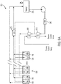
FIG. 9A is a schematic flow diagram of one example of a fluid delivery system to one or more assemblies ofFIG. 1 . -
FIG. 9B is a schematic flow diagram of one example of a grouping of the fluid delivery system ofFIG. 9A . -
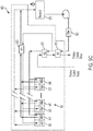
FIG. 9C is a schematic flow diagram of another example of a grouping of the fluid delivery system ofFIG. 9A . -
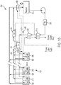
FIG. 10 is a schematic flow diagram of one example of an HBM chiller. -
FIGS. 1 and2 are, respectively, perspective assembled and exploded views of one example of a direct liquid cooledmodule assembly 100.Assembly 100 includes a chip orchip package 200, anorifice plate 300, a manifold 400 and atop plate 500. - A top perspective view of
chip 200 is shown inFIG. 2 .Chip 200 includes various processing components. In one example,chip 200 may be bonded to a carrier substrate or substrate.Chip 200 alone and/or bonded to a substrate may be an integrated circuit ("IC") chip, system on chip ("SoC"), or portion thereof, that may include various passive and active microelectronic devices such as resistors, capacitors, inductors, diodes, metal-oxide semiconductor field effect ("MOSFET") transistors, CMOS transistors, bipolar junction transistors ("BJTs"), laterally diffused metal-oxide-silicon ("LDMOS") transistors, high power MOS transistors, other types of transistors, or other types of devices.Chip 200 may comprise a memory device, a logic device, or other types of circuits, as examples. The substrate thatchip 200 may be bonded to can be, for example, a silicon substrate, a plastic substrate, a flexible substrate having polyimide and copper layers for example, a laminate substrate, a ceramic substrate, an interposer, or any other suitable support structure. - In the example shown, the processing components of
chip 200 areHBMs 202 and anASIC 204. In the present example, there are fourHBMs 202 and onecentral ASIC 204. A portion of the perimeter of each of theHBMs 202 andASIC 204 together form a chip periphery orperimeter 206. The processing components ofchip 200 are located on atop surface 208 ofchip 200. EachHBM 202 lies adjacent anotherHBM 202 and a portion ofASIC 204. In other examples,chip 200 can include more or less HBMs and ASICs and can be located onchip 200 in other configurations.Perimeter 206 can be atop surface 208 of a substrate thatchip 200 is bonded to orperimeter 206 can be thetop surface 208 ofchip 200 itself. In one example,perimeter 206 can be the perimeter of bothbottom surface 207 andtop surface 208 ofchip 200. Any portion oftop surface 208 that is not enclosed byperimeter 206 may be referred to as "dead space" onchip 200 and/or the substrate thatchip 200 is bonded to in that there are no processing components located in the portion oftop surface 208. Because there are no processing components located in this area, this area is preferable for loading of other direct liquid cooled module system components and using this area as a base for applying sealing features, for example. A direct liquid cooled module generally functions to bring coolant to the components of the chip. The module is generally hermetically sealed so that the coolant may only be expelled from the system through an outlet. If coolant is supposed to be introduced to components of the chip to provide a cooling effect, it is generally not preferable to apply a seal directly on the components such that the coolant cannot directly access the components. Theperimeter 206 is therefore a preferred location ontop surface 208 to provide a seal such that coolant can be directly applied to the components of the chip. - While
FIG. 1 shows assembly 100,chip 200 andorifice plate 300 cannot be seen in this assembled view. When viewing the orientation of the assembly components in explodedFIG. 2 , it can be understood that when assembled together,top surface 208 ofchip 200 is sealed to abottom surface 307 oforifice plate 300,top surface 308 oforifice plate 300 is sealed to abottom surface 407 ofmanifold 400, and atop surface 408 ofmanifold 400 is sealed to abottom surface 507 oftop plate 500. Whentop surface 308 oforifice plate 300 is sealed to abottom surface 407 ofmanifold 400, the locations ontop surface 308 oforifice plate 300 where there is sealing is represented byouter seal perimeter 338 andinner seal perimeter 348. Whenbottom surface 507 oforifice plate 300 is sealed to atop surface 408 ofmanifold 400, the locations ontop surface 408 ofmanifold 400 where there is sealing is represented byperimeter seals FIGS. 1 and2 are three arrows that represent the direction of fluid entering intorespective inlets outlet 550 oftop plate 500. The flow of liquid throughassembly 100 will be discussed in greater detail below. -
FIGS. 3A and 3B are respective top and bottom perspective views of one example oforifice plate 300 ofassembly 100 shown inFIG. 2 .Orifice plate 300 has a perimeter or periphery 306, abottom surface 307 and atop surface 308.Orifice plate 300 includes a plurality ofsupply apertures 310 and returnapertures 320 that extend throughorifice plate 300. Each ofsupply apertures 310 and returnapertures 320 extend fromtop surface 308 oforifice plate 300 and intorespective cavities bottom surface 307 oforifice plate 300. As shown inFIG. 3B ,cavities 315 are located in the areas aboveHBMs 202 andcavity 325 will be in the area aboveASIC 204 when chip 20 andorifice plate 300 are sealed together. A plurality ofsupply apertures 310 and at least one return aperture leads into eachcavity 315.Several supply apertures 310 and returnapertures 320 are located withincavity 325. In other examples, there may be more or less supply and returnapertures cavities - The plurality of
supply apertures 310 are for receiving fluid flowing frommanifold 400 to thetop surface 308 oforifice plate 300. Thesesupply apertures 310 may also be referred to as impinging jets. Thesupply apertures 310 are an array of small diameter holes placed in particular locations throughorifice plate 300. A relatively high pressure differential, for example from 5 to greater than 100 psi is applied across thetop surface 308 oforifice plate 300. This creates high velocity water jets through the small diameter holes orsupply apertures 310. In one example, these jets impinge on atop surface 208 ofchip 200 creating a high heat transfer coefficient. - In one example,
orifice plate 300 can cool a total chip area of approximately 20-30mm x 30-50mm. In other examples,orifice plate 300 can be designed to cool a total chip area greater or less than 20-30mm x 30-55mm. Thebottom surface 307 oforifice plate 300 includes a groove 340 (shown for example inFIG. 7 ) for receipt of an O-ring orgasket 350.Groove 340 is designed such that at least a portion of a portion of O-ring orgasket 350 is received within thegroove 340. Whenbottom surface 307 oforifice plate 300 comes into direct contact withtop surface 208 ofchip 200, O-ring orgasket 350 makes a hermetic seal betweenchip 200 andorifice plate 300. - As shown in
FIG. 3B ,gasket 350 forms a window pane arrangement to create a hermetic seal between chip components, namelyHBMs 202 andASIC 204. These components may be bonded to chip 200 with an epoxy type material that is not generally compatible with water and therefore the window pane arrangement ofgasket 350 forms a protective seal around the respective perimeters of these components. - The array of small diameter holes or
supply apertures 310 correspond to high velocity jet locations. In one example, the high velocity jets are created from the pressure differential between thehigh pressure cavities FIG. 6A for example, andlow pressure cavities FIGS 3B , betweenchip 200 andorifice plate 300. In one example, thesmall holes 310 can be spaced between 0.5 & 2mm over high power density regions of thechip 200 and 2mm to 5mm over the regions ofchip 200 with lower power density. In one example, the diameter ofholes 310 is between approximately 50 to 300 microns. In other example, the diameter ofholes 310 may be smaller than 50 micron or larger than 300 micron. -
Orifice plate 300 includes larger diameter holes or a plurality ofreturn apertures 320, into which returntubes 360 may be inserted to connectcavities orifice plate 300 and lowerpressure return reservoir 425 ofmanifold 400, shown inFIG. 6A for example. In one example, the diameter ofholes 320 can be from 500 micron to 4mm in diameter. In other examples, the diameter ofholes 320 may be smaller than 500 micron or larger than 4mm. Generally, holes 320 are separated from the edge of eachcavity - Placement of the large diameter holes 320 is designed based on the longitudinal distance from
orifice plate 300 totop surface 208 ofchip 200, which is approximately 500 micron to 2mm. Since this clearance is low, bulk fluid flow may interact with the jets or small diameter holes 310 and impede the fluid velocity that interacts withtop surface 208 of chip, which may lead to a decrease in the heat transfer coefficient. -
FIG. 4 is a cross-sectional view of one example of anorifice plate 300 coupled to achip package 200.Gasket 350 is shown withingroove 340 of orifice plate. In this example,gasket 350 is shown covering an edge of anHBM 202 and edge of anASIC 204 and anovermold 203 located betweenHBM 202 andASIC 204. Anarea 205 is shown encompassing the edge of anHBM 202, edge of anASIC 204 andovermold 203. An example of an edge jet orsupply aperture 310 is shown near an edge ofASIC 204.Other supply apertures 310 are shown in a more central portion of bothHBM 202 andASIC 204. Also shown arereturn tubes 360 each within a large hole or returnaperture 320. Eachreturn tube 360 lies adjacent one oflow pressure cavities respective cavities supply aperture 310 exits thecavities return tubes 360. -
FIG. 5 is an exploded bottom perspective view of atop plate 500, a manifold 400 and anorifice plate 300 of the directliquid module assembly 100 ofFIG. 1 . In this figure, it is seen howorifice plate 300 lines up withmanifold 400.Orifice plate 300 is shown with eightperipheral apertures 370 that line up with corresponding eightrecesses 475 inbottom surface 407 ofmanifold 400. Fasteners (not shown) can be inserted through eachaperture 370 inorifice plate 300 and into acorresponding recess 475 ofmanifold 400 to aid in the securing oforifice plate 300 andmanifold 400. - In
FIG. 5 ,orifice plate 300 has some transparency that you can see some of thereturn tubes 360 while viewing the bottom surface oforifice plate 300.FIG. 3A shows eachreturn tube 360 coupled to eachreturn aperture 320 oforifice plate 300. In this example, there is onereturn tube 360 corresponding to each location of fourHBMs 202 and there are thirteenreturn tubes 360 corresponding to the location ofASIC 204. The fourreturn tubes 360 located in theHBM 202 locations are received in anouter cavity 435 ofmanifold 400 while the thirteenreturn tubes 360 located in theASIC 204 location are received in aninner cavity 445 ofmanifold 400 whenorifice plate 300 is sealed tomanifold 400. Also shown inFIG. 5 is abottom surface 507 oftop plate 500. Where fluid exitsinlets outlet 550 oftop plate 500 can also be seen by viewingbottom surface 507 oftop plate 500. There are twelveperipheral apertures 580 that line up with corresponding recesses 470 (shown inFIG. 6A ) intop surface 408 ofmanifold 400. Fasteners (not shown) can be inserted through eachaperture 580 intop plate 500 and into acorresponding recess 470 ofmanifold 400 to aid in the securing oftop plate 500 andmanifold 400.Manifold 400 also includes fourperipheral apertures 480 in which fasteners (not shown) can be inserted to aid in the securing of manifold to other components of the direct liquid cooled module such as a bolsterplate 600, for example, shown inFIG. 8 . -
FIGS. 6A-6D are various views of one example of amanifold 400 of theassembly 100 shown inFIG. 1 . As shown inFIGS. 6A and 6B ,manifold 400 includes lowpressure return reservoir 425 between a first highpressure supply reservoir 455 and a second highpressure supply reservoir 465.Reservoir 455 includes anelongate opening 457 andreservoir 465 includes anelongate opening 468. An arrow inreservoir 455 shows the direction of fluid flow fromreservoir 455 throughopening 457 while an arrow inreservoir 465 shows the direction of fluid fromreservoir 465 throughopening 468. Fluid flowing through opening 457 fromreservoir 455 enters intoinner cavity 445 while fluid flowing through opening 468 fromreservoir 465 enters intoouter cavity 435. Fluid then flows frominner cavity 445 ontotop surface 308 oforifice plate 300 and throughsupply apertures 310 and intocavity 325 leading toASIC 204 ofchip 200. Fluid also then flows fromouter cavity 435 ontotop surface 308 oforifice plate 300 and throughsupply apertures 310 and intocavities 315 leading toHBMs 202 ofchip 200. All fluid incavities respective return tubes 360 and exits a second end of return tubes coupled to returnapertures 420 into lowpressure return reservoir 425 ofmanifold 400. - Surrounding
outer cavity 435 andinner cavity 445 arerespective grooves bottom surface 407 ofmanifold 400. An O-ring orgasket 432 is at least partially received withingroove 438 ofouter cavity 435 and an O-ring orgasket 442 is at least partially received withingroove 448 ofinner cavity 445. Whenbottom surface 407 of manifold is sealed totop surface 308 oforifice plate 300, all returntubes 360 are contained within the perimeter ofgroove 438 and the four outer return tubes 460 are contained withinouter cavity 435, while the thirteen inner return tubes 460 are contained both within the perimeter ofgroove 448 andinner cavity 445. - Surrounding each of low
pressure return reservoir 425, first highpressure supply reservoir 455, and second highpressure supply reservoir 465 arerespective grooves respective grooves FIG. 2 . Whenbottom surface 507 oftop plate 500 is in direct contact withtop surface 408 of manifold, each of O-ring or gasket 422, 452 and 462 are in direction contact withbottom surface 507 oftop plate 500 to hermetically seal the respective lowpressure return reservoir 425, first highpressure supply reservoir 455, and second highpressure supply reservoir 465. - While
grooves grooves -
FIG. 7 is a cross-sectional perspective assembled view oforifice plate 300,manifold 400 andtop plate 500 whileFIG. 8 is a cross-sectional assembled view of each of these system components including additional components of the system such aschip 200, and a bolsterplate 600. InFIG. 7 , a curved arrow shows an example fluid path of fluid that entered the system throughinlet 530 oftop plate 500 and intoreservoir 455. Fromreservoir 455 the fluid flows through opening 457 ofreservoir 455 and intoinner cavity 445 before flowing throughsupply apertures 310 oforifice plate 300. Once throughorifice plate 300, the fluid enters intocavity 325 and then onto the surface ofASIC 204 ofchip 200, which is shown inFIG. 8 . Fluid withincavity 325 then enters thereturn tubes 360 located within the perimeter ofcavity 325 oforifice plate 300 and exits into lowpressure return reservoir 425 ofmanifold 400 before then flowing out ofoutlet 550 oftop plate 500. - Also shown in
FIGS. 7 and8 is an example fluid path of fluid that entered the system throughinlet 540 oftop plate 500 and intoreservoir 465. Fromreservoir 465 the fluid flows through opening 468 ofreservoir 465 and intoouter cavity 435 before flowing throughsupply apertures 310 oforifice plate 300. Once throughorifice plate 300, the fluid enters intocavities 315 oforifice plate 300 and then onto the surface ofHBMs 202 ofchip 200, which is shown inFIG. 8 . Fluid withincavities 315 then enters thereturn tubes 360 located within the perimeters ofcavities 315 and exits into lowpressure return reservoir 425 ofmanifold 400 before then flowing out ofoutlet 550 oftop plate 500. - This system includes two supply lines and a common return line. The main supply line, which may be referred to as
inlet 530 directs approximately 80-95% of the fluid flow to a component ofchip 200 such asASIC 204, for example. The components ofchip 200 that are fed fluid from the main supply line generally consume most of the power ofchip 200. A second supply line, which may be referred to aninlet 540 directs approximately 5-20% of the fluid flow to other components ofchip 200 such as one ormore HBMs 202. AnHBM 202 is generally more sensitive to temperature and may require lower temperature fluid than anASIC 204, for example. Since the percentage of flow is less in the second supply line, it can be more cost effective to deliver a colder supply of water through the second supply line than to provide that lower temperature water to theentire package assembly 100, including for example, bothHBMs 202 and one ormore ASICs 204. There is a common return, which may be referred to asoutlet 550 where the fluid flow mixes from all components ofchip 200 such asHBMs 202 andASIC 204. - In other examples,
system 100 can have other configurations.System 100 can have a single supply line and a single return, instead of the previously described example ofsystem 100 have two supply lines and a single return. In another example,system 100 can have two supply lines and two returns. In other examples,system 100 can have one or two supply lines and more than two returns. In other examples,system 100 can have one or two returns and more than two supply lines. In yet other examples,system 100 can have more than two supply lines and more than two returns. - In other examples,
chip 200 can have various other configurations of components, such as one or more HBMs, ASICs and chiplets. In other examples, O-rings and gaskets used to create hermetic seals betweenchip 200 andorifice plate 300,orifice plate 300 andmanifold 400, andmanifold 400 andtop plate 500 could be located only around the respective perimeters of each of the features ofsystem 100. In such a case, the mold material used to bond components to chip 200 may be allowed to be wetted instead of covered by an O-ring or gasket as shown, for example, inFIG. 4 . In another example, a window gasket may be used if there are two supply lines and two returns and one pair of supply lines and returns operates with colder fluid and the other pair of supply lines and returns operates with warmer fluid. -
FIG. 9A is a schematic flow diagram of one example of afluid delivery system 800 to one or more chip packages 900. Each chip package has at least onefirst chip component 920 and asecond chip component 940. In one example,first chip component 920 is one or more ASICs andsecond chip component 940 is one or more HBMs. However, it should be understood that the chip components may include any combination of a variety of chips, such as GPUs, ASICs, etc., in any number or configuration. Coolant in the form of fluid is supplied tosystem 800 from a lab chiller, for example. In one example, coolant supplied tosystem 800 is 16°C. The coolant then enters asecond heat exchange 820 and mixes with higher temperature coolant supplied from afirst heat exchange 810. Fluid either exitsheat exchange 820 to travel to asecond chip component 940 or travels tofirst heat exchange 810. In one example, approximately 10% of the coolant that is supplied tosystem 800 exitsheat exchange 810 to travel tosecond chip component 940. In this example, the coolant that travels tosecond chip component 940 is 17°C. While in other examples, the coolant supplied tosystem 800 can be more or less than 16°C and the coolant supplied tosecond chip component 940 can be more or less than 17°C, there is generally a low temperature differential between the coolant supplied tosystem 800 and the coolant supplied tosecond chip component 940. It should be understood that the foregoing is merely an example, and that the percentage of coolant fromheat exchange 810 supplied to thesecond chip component 940 may be varied, and the temperature of the coolant supplied to each component may be varied. - The coolant that enters
first heat exchange 810 fromsecond heat exchange 820 mixes with fluid that is returned from previously cooling offirst chip component 920. In one example, the fluid returned from previous cooling of both first andsecond chip components first heat exchange 810 at approximately 35°C. In this example, the coolant that entersfirst heat exchange 810 either exitsfirst heat exchange 810 to a coolant return at approximately 32°C or exitsfirst heat exchange 810 at approximately 34.5°C before flowing to athird heat exchange 830. Approximately 90% of the fluid flow insystem 800 flows tofirst chip component 920. There is a very low temperature differential (approximately .5°C) between the fluid returned from previous cooling and the fluid that travels to thethird heat exchange 830. In other examples, the coolant that exitsfirst heat exchange 810 to a coolant return can be more or less than 32°C, the coolant that exitsfirst heat exchange 810 before flowing to athird heat exchange 830 can be more or less than 34.5°C, and the fluid or coolant returned from previous cooling of both first andsecond chip components first heat exchange 810 at more or less than 35°C. As mentioned above, such values for the percentage of fluid flow and temperatures of coolant are merely examples and may be varied. - As further shown in
FIG. 9A ,third heat exchange 830 exchanges heat with fluid flowingfirst chip component 920 with fluid returning from coolingsecond chip component 940. Here, warmer fluid flowing tofirst chip component 920 or ASICs mixes with cooler fluid returning fromsecond chip component 940 or HBMs. Fluid exitingfirst chip component 920 then travels to areservoir 970 and then to afilter 980 before enteringfirst heat exchange 810. Fluid exitingthird heat exchange 830 mixes with fluid that has exitingfirst chip component 920 before enteringreservoir 970 and together flowing to filter 980 before enteringfirst heat exchange 810. -
FIGS. 9B and9C are schematic flow diagrams including example groupings of components offluid delivery system 800. The groupings may enable use of a common pump, reservoir, and/or filter for a plurality of machines. - In the example of
FIG. 9B ,first chip component 920 andsecond chip component 940 are grouped together while all other components ofsystem 800 are grouped together such as first, second andthird heat exchangers reservoir 970 andfilter 980. As the heat exchangers 810-830 are grouped with the pump, reservoir, and filter, they could support multiples of the other grouping, which in this example includes several instances of a plurality of jet manifolds. Such grouping may reduce hardware costs for heat exchangers. However, it may also result in reduced control of flow. - In the example of
FIG. 9C , all of the components ofsystem 800 are grouped together in a first group other thanreservoir 970 and filter 980 which are grouped together in a second group. For example, several instances of the group including the heat exchangers 810-830 and the manifolds may use acommon reservoir 970,filter 980, and pump. Such groupings can provide for a better ability to control and optimize the amount of process coolant required at the expense of more heat exchangers. -
FIG. 10 is a schematic flow diagram of one example of an HBM chiller added tosystem 800. In this example, the HBM chiller is a refrigeration circuit which includescondenser 880,evaporator 860, andexpansion valve 882. The HBM chiller removes heat and chills liquid that passes through theevaporator 860 and pumps that heat into thecondenser 880. The HBM chiller may be implemented, for example, to sub cool the HBM only. The HBM portion can represent approximately 10-20% of the heat in some examples. Accordingly, cooling only the HBM portion requires much less chiller capacity than cooling all flow to that level. In this example, afourth heat exchange 840 receives fluid exitingsecond heat exchange 820. Thefourth heat exchange 840 also receives fluid that has exited from cooling one or moresecond chip components 940. Some of the fluid exiting thefourth heat exchange 840 does not flow directly to one or moresecond chip components 940 and instead enters into anevaporation chamber 860, the output of which flows to acondenser 880 and back to theevaporation chamber 860 in a cycle. - Another aspect of the present disclosure relates to systems and methods for chip cooling with near edge jets in a direct liquid cooled module. One of the functions of a direct liquid cooled module is to provide cooling liquid to components located on a chip. Jet impingement directly onto the back side of a chip is one cooling method that can provide more efficient cooling. An orifice plate includes an array of small diameter holes that correspond to high velocity jet locations and large diameter holes for the insertion of tubes to connect to lower pressure cavities.
- Unless otherwise stated, the foregoing alternative examples are not mutually exclusive, but may be implemented in various combinations to achieve unique advantages. As these and other variations and combinations of the features discussed above can be utilized without departing from the subject matter defined by the claims, the foregoing description should be taken by way of illustration rather than by way of limitation of the subject matter defined by the claims. In addition, the provision of the examples described herein, as well as clauses phrased as "such as," "including" and the like, should not be interpreted as limiting the subject matter of the claims to the specific examples; rather, the examples are intended to illustrate only one of many possible implementations. Further, the same reference numbers in different drawings can identify the same or similar elements.
Claims (15)
- An assembly, comprising:an orifice plate having top and bottom surfaces and a plurality of supply and return apertures, the plurality of supply apertures for receiving fluid flowing through the plate from the top surface to the bottom surface, the bottom surface of the orifice plate adapted to be sealed to a top surface of a substrate containing circuitry;a coolant delivery manifold having top and bottom surfaces and at least one supply cavity in fluid communication with at least a subset of the plurality of supply apertures, and at least one return cavity in fluid communication with the plurality of return apertures; anda first sealing member forming a hermetic seal between the top surface of the plate and the bottom surface of the manifold.
- The assembly of claim 1, wherein the bottom surface of the coolant delivery manifold has an outer groove, the outer groove forming an outer closed perimeter adapted to receive at least a portion of the first sealing member therein.
- The assembly of claim 2, wherein when the top surface of the plate is sealed to the bottom surface of the coolant delivery manifold all of the plurality of supply and return apertures of the plate are contained within the outer closed perimeter of the outer groove of the coolant delivery manifold.
- The assembly of claim 2 or 3, wherein the bottom surface of the manifold has an inner groove, the inner groove forming an inner closed perimeter at least partially surrounded by the outer closed perimeter and adapted to receive at least a portion of a second sealing member therein.
- The assembly of claim 4, wherein when the top surface of the plate is sealed to the bottom surface of the manifold at least a subset of the plurality of supply and return apertures of the plate are contained within the inner closed perimeter of the inner groove of the manifold.
- The assembly of any one of claims 1 to 5, further comprising a plurality of return tubes directly connecting the at least one return cavity of the manifold with the plurality of return apertures of the plate, and/or
a third sealing member adapted to create a hermetic seal between the bottom surface of the plate and to the top surface of the substrate. - The assembly of claim 6, wherein the bottom surface of the plate has a groove, the groove forming a closed outer perimeter adapted to receive at least a portion of the third sealing member therein, and
wherein optionally all of the plurality of supply and return apertures of the plate are located within the closed outer perimeter of the groove when the plate is sealed to the substrate. - A coolant delivery manifold, comprising:a top surface including at least one supply cavity and at least one return cavity; anda bottom surface including an inner cavity and a surrounding outer cavity,wherein each of the at least one supply cavities includes an opening between a bottom portion of the supply cavity and at least one of the inner cavity or the surrounding outer cavity on the bottom surface, the opening adapted for transmission of fluid at a first temperature through the supply cavity to the inner cavity and transmission of a fluid at a second temperature different than the first temperature to the surrounding outer cavity, andwherein the at least one return cavity includes a plurality of apertures between the inner cavity on the bottom surface and the top surface, the plurality of apertures sized to receive a plurality of fluid return tubes.
- The coolant delivery manifold of claim 8, wherein the bottom surface of the manifold is adapted to be coupled to a top surface of an orifice plate, and wherein a bottom surface of the orifice plate is adapted to be sealed to a top surface of a substrate containing circuitry, and
wherein optionally the substrate has first and second circuitry regions, the first circuitry region corresponding to the inner cavity of the coolant delivery manifold, and the second circuitry region corresponding to the outer surrounding cavity of the coolant delivery manifold. - The coolant delivery manifold of claim 9, wherein the orifice plate includes a groove including a first closed perimeter and a second closed perimeter, and
wherein optionally when the orifice plate is sealed to the substrate at least a portion of the first circuitry region is located within the first closed perimeter of the groove and at least a portion of the second circuitry region is located within the second closed perimeter of the groove. - The coolant delivery manifold of any one of claims 8 to 10, further comprising a sealing member forming a seal between the bottom surface of the manifold and the top surface of the orifice plate.
- The coolant delivery manifold of any one of claims 8 to 11, further comprising a plurality of return tubes directly connecting the at least one return cavity of the manifold with a plurality of return apertures in the orifice plate.
- An assembly, comprising:an orifice plate having top and bottom surfaces and a plurality of supply and return apertures, the bottom surface of the plate adapted to seal to a top surface of a semiconductor containing circuitry, the plurality of supply and return apertures in fluid communication with the circuitry when the plate and substrate are sealed together,wherein the bottom surface of the plate has at least one cavity having an internal wall about a perimeter of the cavity, andwherein at least some of the plurality of supply apertures are proximate the internal wall of the at least one cavity.
- The assembly of claim 13, further comprising:a manifold having top and bottom surfaces and at least one supply cavity in fluid communication with at least a portion of the plurality of supply apertures and at least one return cavity in fluid communication with the plurality of return apertures; anda sealing member adapted to create a hermetic seal between the plate and the manifold.
- The assembly of claim 13 or 14, further comprising a second sealing member positioned about the perimeter of the at least one cavity on the bottom surface of the plate, and
wherein optionally the second sealing member creates a seal between the plate and a substrate including one or more chips.
Applications Claiming Priority (1)
| Application Number | Priority Date | Filing Date | Title |
|---|---|---|---|
| US16/887,122 US11310937B2 (en) | 2020-05-29 | 2020-05-29 | Impinging jet manifold for chip cooling near edge jets |
Publications (2)
| Publication Number | Publication Date |
|---|---|
| EP3916777A1 true EP3916777A1 (en) | 2021-12-01 |
| EP3916777B1 EP3916777B1 (en) | 2024-05-15 |
Family
ID=73726542
Family Applications (1)
| Application Number | Title | Priority Date | Filing Date |
|---|---|---|---|
| EP20211029.2A Active EP3916777B1 (en) | 2020-05-29 | 2020-12-01 | Impinging jet manifold for chip cooling near edge jets |
Country Status (6)
| Country | Link |
|---|---|
| US (1) | US11310937B2 (en) |
| EP (1) | EP3916777B1 (en) |
| CN (1) | CN112185918B (en) |
| DK (1) | DK3916777T3 (en) |
| FI (1) | FI3916777T3 (en) |
| TW (1) | TWI840627B (en) |
Families Citing this family (32)
| Publication number | Priority date | Publication date | Assignee | Title |
|---|---|---|---|---|
| USD957568S1 (en) * | 2020-06-25 | 2022-07-12 | Wellis USA Inc. | Spa jet multiport |
| US11963328B2 (en) * | 2020-10-13 | 2024-04-16 | Raytheon Company | Electronic component connector cooling device |
| EP4386833A4 (en) * | 2021-10-27 | 2024-11-13 | Huawei Technologies Co., Ltd. | HEAT DISSIPATION SYSTEM, ELECTRONIC DEVICE AND LIQUID COOLING SYSTEM |
| CN116075111B (en) * | 2021-11-04 | 2025-09-02 | 英业达科技有限公司 | Coolant flow control device |
| CN116133317A (en) * | 2021-11-12 | 2023-05-16 | 英业达科技有限公司 | Coolant flow control device |
| WO2023147502A1 (en) * | 2022-01-31 | 2023-08-03 | Adeia Semiconductor Bonding Technologies Inc. | Heat dissipating system for electronic devices |
| US12191233B2 (en) | 2022-07-28 | 2025-01-07 | Adeia Semiconductor Bonding Technologies Inc. | Embedded cooling systems and methods of manufacturing embedded cooling systems |
| TWI872720B (en) * | 2022-09-26 | 2025-02-11 | 銓心半導體異質整合股份有限公司 | Semiconductor package structure for enhanced cooling |
| CN115548838B (en) * | 2022-11-04 | 2023-03-24 | 中国航天三江集团有限公司 | Cooling and heat dissipation device and method for single-chip-level jet impact optical element |
| WO2024138186A1 (en) | 2022-12-23 | 2024-06-27 | Adeia Semiconductor Bonding Technologies Inc. | Embedded cooling systems for advanced device packaging |
| CN120457540A (en) | 2022-12-29 | 2025-08-08 | 美商艾德亚半导体接合科技有限公司 | Embedded cooling assembly for advanced device package and method of manufacturing the same |
| CN120513517A (en) | 2022-12-31 | 2025-08-19 | 美商艾德亚半导体接合科技有限公司 | Embedded liquid cooling |
| US12341083B2 (en) | 2023-02-08 | 2025-06-24 | Adeia Semiconductor Bonding Technologies Inc. | Electronic device cooling structures bonded to semiconductor elements |
| TW202516697A (en) | 2023-03-31 | 2025-04-16 | 美商艾德亞半導體接合科技有限公司 | Integrated cooling assemblies including backside power/ground delivery and methods of manufacturing the same |
| CN118841379A (en) * | 2023-04-25 | 2024-10-25 | 华为技术有限公司 | Chip packaging structure and electronic equipment |
| US12191235B2 (en) | 2023-05-17 | 2025-01-07 | Adeia Semiconductor Bonding Technologies Inc. | Integrated cooling assemblies including signal redistribution and methods of manufacturing the same |
| US12191234B2 (en) | 2023-05-17 | 2025-01-07 | Adeia Semiconductor Bonding Technologies Inc. | Integrated cooling assemblies for advanced device packaging and methods of manufacturing the same |
| CN117412571B (en) * | 2023-11-29 | 2024-06-07 | 广东液冷时代科技有限公司 | Nanofluid immersion type jet cooling device based on EHD conduction and control method |
| US12610819B2 (en) | 2023-12-21 | 2026-04-21 | Adeia Semiconductor Bonding Technologies Inc. | Integrated cooling assemblies for advanced device packaging and methods of manufacturing the same |
| US12283490B1 (en) | 2023-12-21 | 2025-04-22 | Adeia Semiconductor Bonding Technologies Inc. | Integrated cooling assemblies for advanced device packaging and methods of manufacturing the same |
| US12368087B2 (en) | 2023-12-26 | 2025-07-22 | Adeia Semiconductor Bonding Technologies Inc. | Embedded cooling systems for advanced device packaging and methods of manufacturing the same |
| US12322677B1 (en) | 2024-02-07 | 2025-06-03 | Adeia Semiconductor Bonding Technologies Inc. | Fluid channel geometry optimizations to improve cooling efficiency |
| US12525506B2 (en) | 2024-02-07 | 2026-01-13 | Adeia Semiconductor Bonding Technologies Inc. | Embedded cooling systems for advanced device packaging and methods of manufacturing the same |
| US12336141B1 (en) | 2024-03-29 | 2025-06-17 | Adeia Semiconductor Bonding Technologies Inc. | Cold plate cavity designs for improved thermal performance |
| US12532432B2 (en) | 2024-03-29 | 2026-01-20 | Adeia Semiconductor Bonding Technologies Inc. | Hotspot mitigation in fluid cooling |
| US12176264B1 (en) | 2024-03-29 | 2024-12-24 | Adeia Semiconductor Bonding Technologies Inc. | Manifold designs for embedded liquid cooling in a package |
| US12500138B2 (en) | 2024-04-17 | 2025-12-16 | Adeia Semiconductor Bonding Technologies Inc. | Cooling channel shape with substantially constant cross sectional area |
| US12266545B1 (en) | 2024-05-24 | 2025-04-01 | Adeia Semiconductor Bonding Technologies Inc. | Structures and methods for integrated cold plate in XPUs and memory |
| CN118899275A (en) * | 2024-06-21 | 2024-11-05 | 浙江日虹变频器有限公司 | IGBT module water-cooling heat dissipation structure and water-cooling inverter having the same |
| CN121666080A (en) * | 2024-08-30 | 2026-03-13 | 华为技术有限公司 | Radiator, electronic equipment and communication equipment |
| US12412808B1 (en) | 2024-12-20 | 2025-09-09 | Adeia Semiconductor Bonding Technologies Inc. | Cold plate and manifold integration for high reliability |
| US12513855B1 (en) | 2025-03-07 | 2025-12-30 | Adeia Semiconductor Bonding Technologies Inc. | Integrated cooling assembly with upper and lower channels |
Citations (2)
| Publication number | Priority date | Publication date | Assignee | Title |
|---|---|---|---|---|
| US20060266497A1 (en) * | 2005-05-25 | 2006-11-30 | International Business Machines Corporation | High performance integrated mlc cooling device for high power density ics and method for manufacturing |
| US10334755B2 (en) * | 2015-12-30 | 2019-06-25 | Imec Vzw | Liquid cooling of electronic devices |
Family Cites Families (33)
| Publication number | Priority date | Publication date | Assignee | Title |
|---|---|---|---|---|
| US5269372A (en) * | 1992-12-21 | 1993-12-14 | International Business Machines Corporation | Intersecting flow network for a cold plate cooling system |
| JP2003051689A (en) * | 2001-08-06 | 2003-02-21 | Toshiba Corp | Cooling device for heating element |
| US20040112571A1 (en) * | 2002-11-01 | 2004-06-17 | Cooligy, Inc. | Method and apparatus for efficient vertical fluid delivery for cooling a heat producing device |
| US7277283B2 (en) * | 2005-05-06 | 2007-10-02 | International Business Machines Corporation | Cooling apparatus, cooled electronic module and methods of fabrication thereof employing an integrated coolant inlet and outlet manifold |
| US7233494B2 (en) * | 2005-05-06 | 2007-06-19 | International Business Machines Corporation | Cooling apparatus, cooled electronic module and methods of fabrication thereof employing an integrated manifold and a plurality of thermally conductive fins |
| US7298618B2 (en) * | 2005-10-25 | 2007-11-20 | International Business Machines Corporation | Cooling apparatuses and methods employing discrete cold plates compliantly coupled between a common manifold and electronics components of an assembly to be cooled |
| US7298617B2 (en) | 2005-10-25 | 2007-11-20 | International Business Machines Corporation | Cooling apparatus and method employing discrete cold plates disposed between a module enclosure and electronics components to be cooled |
| US7511957B2 (en) * | 2006-05-25 | 2009-03-31 | International Business Machines Corporation | Methods for fabricating a cooled electronic module employing a thermally conductive return manifold structure sealed to the periphery of a surface to be cooled |
| US7362574B2 (en) | 2006-08-07 | 2008-04-22 | International Business Machines Corporation | Jet orifice plate with projecting jet orifice structures for direct impingement cooling apparatus |
| US7762314B2 (en) * | 2007-04-24 | 2010-07-27 | International Business Machines Corporation | Cooling apparatus, cooled electronic module and methods of fabrication employing a manifold structure with interleaved coolant inlet and outlet passageways |
| US8046113B2 (en) * | 2007-07-27 | 2011-10-25 | Hewlett-Packard Development Company, L.P. | System and method for cooling a heat-generating device |
| US7639030B2 (en) | 2007-10-15 | 2009-12-29 | Intel Corporation | Creating a jet impingement pattern for a thermal control system |
| US8081461B2 (en) | 2009-06-25 | 2011-12-20 | International Business Machines Corporation | Cooling apparatus with thermally conductive porous material and jet impingement nozzle(s) extending therein |
| US8077460B1 (en) * | 2010-07-19 | 2011-12-13 | Toyota Motor Engineering & Manufacturing North America, Inc. | Heat exchanger fluid distribution manifolds and power electronics modules incorporating the same |
| US9252069B2 (en) | 2010-08-31 | 2016-02-02 | Teledyne Scientific & Imaging, Llc | High power module cooling system |
| US8199505B2 (en) | 2010-09-13 | 2012-06-12 | Toyota Motor Engineering & Manufacturing Norh America, Inc. | Jet impingement heat exchanger apparatuses and power electronics modules |
| US8427832B2 (en) | 2011-01-05 | 2013-04-23 | Toyota Motor Engineering & Manufacturing North America, Inc. | Cold plate assemblies and power electronics modules |
| US9484283B2 (en) * | 2013-01-04 | 2016-11-01 | Toyota Motor Engineering & Manufacturing North America Inc. | Modular jet impingement cooling apparatuses with exchangeable jet plates |
| US9460985B2 (en) * | 2013-01-04 | 2016-10-04 | Toyota Motor Engineering & Manufacturing North America, Inc. | Cooling apparatuses having a jet orifice surface with alternating vapor guide channels |
| US9835363B2 (en) | 2013-01-14 | 2017-12-05 | Massachusetts Institute Of Technology | Evaporative heat transfer system |
| US9247672B2 (en) | 2013-01-21 | 2016-01-26 | Parker-Hannifin Corporation | Passively controlled smart microjet cooling array |
| US9265176B2 (en) * | 2013-03-08 | 2016-02-16 | International Business Machines Corporation | Multi-component electronic module with integral coolant-cooling |
| US8981556B2 (en) * | 2013-03-19 | 2015-03-17 | Toyota Motor Engineering & Manufacturing North America, Inc. | Jet impingement cooling apparatuses having non-uniform jet orifice sizes |
| US9131631B2 (en) | 2013-08-08 | 2015-09-08 | Toyota Motor Engineering & Manufacturing North America, Inc. | Jet impingement cooling apparatuses having enhanced heat transfer assemblies |
| US9445526B2 (en) | 2014-12-22 | 2016-09-13 | Toyota Motor Engineering & Manufacturing North America, Inc. | Modular jet impingement assemblies with passive and active flow control for electronics cooling |
| US9980415B2 (en) * | 2015-08-20 | 2018-05-22 | Toyota Motor Engineering & Manufacturing North America, Inc. | Configurable double-sided modular jet impingement assemblies for electronics cooling |
| US9622380B1 (en) * | 2015-09-30 | 2017-04-11 | Toyota Motor Engineering & Manufacturing North America, Inc. | Two-phase jet impingement cooling devices and electronic device assemblies incorporating the same |
| US20170186667A1 (en) * | 2015-12-26 | 2017-06-29 | Intel Corporation | Cooling of electronics using folded foil microchannels |
| US10566265B2 (en) | 2016-11-18 | 2020-02-18 | Toyota Motor Engineering & Manufacturing North America, Inc. | Electronic assemblies having a cooling chip layer with impingement channels and through substrate vias |
| WO2019018681A1 (en) * | 2017-07-19 | 2019-01-24 | Johnson Controls Technology Company | Electronics cooling system |
| US10668725B2 (en) * | 2018-03-06 | 2020-06-02 | Ricoh Company, Ltd. | Supply manifold in a printhead |
| US20190343020A1 (en) * | 2018-05-01 | 2019-11-07 | General Electric Company | Cooling device with integral shielding structure for an electronics module |
| US10561040B1 (en) * | 2018-10-08 | 2020-02-11 | Hewlett Packard Enterprise Development Lp | Flexible gasket seal for direct liquid cooling of electronic devices |
-
2020
- 2020-05-29 US US16/887,122 patent/US11310937B2/en active Active
- 2020-10-22 CN CN202011138997.9A patent/CN112185918B/en active Active
- 2020-10-30 TW TW109137802A patent/TWI840627B/en active
- 2020-12-01 EP EP20211029.2A patent/EP3916777B1/en active Active
- 2020-12-01 DK DK20211029.2T patent/DK3916777T3/en active
- 2020-12-01 FI FIEP20211029.2T patent/FI3916777T3/en active
Patent Citations (2)
| Publication number | Priority date | Publication date | Assignee | Title |
|---|---|---|---|---|
| US20060266497A1 (en) * | 2005-05-25 | 2006-11-30 | International Business Machines Corporation | High performance integrated mlc cooling device for high power density ics and method for manufacturing |
| US10334755B2 (en) * | 2015-12-30 | 2019-06-25 | Imec Vzw | Liquid cooling of electronic devices |
Also Published As
| Publication number | Publication date |
|---|---|
| CN112185918A (en) | 2021-01-05 |
| TWI840627B (en) | 2024-05-01 |
| TW202145869A (en) | 2021-12-01 |
| FI3916777T3 (en) | 2024-07-18 |
| US11310937B2 (en) | 2022-04-19 |
| CN112185918B (en) | 2025-02-07 |
| EP3916777B1 (en) | 2024-05-15 |
| US20210378139A1 (en) | 2021-12-02 |
| DK3916777T3 (en) | 2024-08-12 |
Similar Documents
| Publication | Publication Date | Title |
|---|---|---|
| EP3916777B1 (en) | Impinging jet manifold for chip cooling near edge jets | |
| US7516776B2 (en) | Microjet module assembly | |
| US11018077B2 (en) | Modular microjet cooling of packaged electronic components | |
| JP5414349B2 (en) | Electronic equipment | |
| US11967541B2 (en) | Liquid-based heat exchanger | |
| AU697411B2 (en) | Apparatus and method for spray-cooling an electronic module | |
| US12272619B2 (en) | Direct liquid cooling with O-ring sealing | |
| EP3913465B1 (en) | Spring loaded compliant coolant distribution manifold for direct liquid cooled modules | |
| US20050128705A1 (en) | Composite cold plate assembly | |
| US20080002363A1 (en) | Direct liquid jet impingement module for high heat flux electronics packages | |
| HK40044422A (en) | Impinging jet manifold for chip cooling near edge jets | |
| HK40044422B (en) | Impinging jet manifold for chip cooling near edge jets | |
| HK40041906A (en) | Spring loaded compliant coolant distribution manifold for direct liquid cooled modules | |
| HK40044423A (en) | Direct liquid cooling with o-ring sealing | |
| HK40041906B (en) | Spring loaded compliant coolant distribution manifold for direct liquid cooled modules |
Legal Events
| Date | Code | Title | Description |
|---|---|---|---|
| PUAI | Public reference made under article 153(3) epc to a published international application that has entered the european phase |
Free format text: ORIGINAL CODE: 0009012 |
|
| STAA | Information on the status of an ep patent application or granted ep patent |
Free format text: STATUS: THE APPLICATION HAS BEEN PUBLISHED |
|
| AK | Designated contracting states |
Kind code of ref document: A1 Designated state(s): AL AT BE BG CH CY CZ DE DK EE ES FI FR GB GR HR HU IE IS IT LI LT LU LV MC MK MT NL NO PL PT RO RS SE SI SK SM TR |
|
| B565 | Issuance of search results under rule 164(2) epc |
Effective date: 20210601 |
|
| STAA | Information on the status of an ep patent application or granted ep patent |
Free format text: STATUS: REQUEST FOR EXAMINATION WAS MADE |
|
| 17P | Request for examination filed |
Effective date: 20220524 |
|
| RBV | Designated contracting states (corrected) |
Designated state(s): AL AT BE BG CH CY CZ DE DK EE ES FI FR GB GR HR HU IE IS IT LI LT LU LV MC MK MT NL NO PL PT RO RS SE SI SK SM TR |
|
| GRAP | Despatch of communication of intention to grant a patent |
Free format text: ORIGINAL CODE: EPIDOSNIGR1 |
|
| STAA | Information on the status of an ep patent application or granted ep patent |
Free format text: STATUS: GRANT OF PATENT IS INTENDED |
|
| INTG | Intention to grant announced |
Effective date: 20231206 |
|
| RAP3 | Party data changed (applicant data changed or rights of an application transferred) |
Owner name: GOOGLE LLC |
|
| GRAS | Grant fee paid |
Free format text: ORIGINAL CODE: EPIDOSNIGR3 |
|
| GRAA | (expected) grant |
Free format text: ORIGINAL CODE: 0009210 |
|
| STAA | Information on the status of an ep patent application or granted ep patent |
Free format text: STATUS: THE PATENT HAS BEEN GRANTED |
|
| AK | Designated contracting states |
Kind code of ref document: B1 Designated state(s): AL AT BE BG CH CY CZ DE DK EE ES FI FR GB GR HR HU IE IS IT LI LT LU LV MC MK MT NL NO PL PT RO RS SE SI SK SM TR |
|
| P01 | Opt-out of the competence of the unified patent court (upc) registered |
Effective date: 20240405 |
|
| REG | Reference to a national code |
Ref country code: CH Ref legal event code: EP |
|
| REG | Reference to a national code |
Ref country code: DE Ref legal event code: R096 Ref document number: 602020030877 Country of ref document: DE |
|
| REG | Reference to a national code |
Ref country code: IE Ref legal event code: FG4D |
|
| REG | Reference to a national code |
Ref country code: FI Ref legal event code: FGE |
|
| REG | Reference to a national code |
Ref country code: NL Ref legal event code: FP |
|
| REG | Reference to a national code |
Ref country code: DK Ref legal event code: T3 Effective date: 20240805 |
|
| REG | Reference to a national code |
Ref country code: SE Ref legal event code: TRGR |
|
| REG | Reference to a national code |
Ref country code: LT Ref legal event code: MG9D |
|
| PG25 | Lapsed in a contracting state [announced via postgrant information from national office to epo] |
Ref country code: IS Free format text: LAPSE BECAUSE OF FAILURE TO SUBMIT A TRANSLATION OF THE DESCRIPTION OR TO PAY THE FEE WITHIN THE PRESCRIBED TIME-LIMIT Effective date: 20240915 |
|
| PG25 | Lapsed in a contracting state [announced via postgrant information from national office to epo] |
Ref country code: BG Free format text: LAPSE BECAUSE OF FAILURE TO SUBMIT A TRANSLATION OF THE DESCRIPTION OR TO PAY THE FEE WITHIN THE PRESCRIBED TIME-LIMIT Effective date: 20240515 |
|
| PG25 | Lapsed in a contracting state [announced via postgrant information from national office to epo] |
Ref country code: HR Free format text: LAPSE BECAUSE OF FAILURE TO SUBMIT A TRANSLATION OF THE DESCRIPTION OR TO PAY THE FEE WITHIN THE PRESCRIBED TIME-LIMIT Effective date: 20240515 |
|
| PG25 | Lapsed in a contracting state [announced via postgrant information from national office to epo] |
Ref country code: GR Free format text: LAPSE BECAUSE OF FAILURE TO SUBMIT A TRANSLATION OF THE DESCRIPTION OR TO PAY THE FEE WITHIN THE PRESCRIBED TIME-LIMIT Effective date: 20240816 |
|
| PG25 | Lapsed in a contracting state [announced via postgrant information from national office to epo] |
Ref country code: PT Free format text: LAPSE BECAUSE OF FAILURE TO SUBMIT A TRANSLATION OF THE DESCRIPTION OR TO PAY THE FEE WITHIN THE PRESCRIBED TIME-LIMIT Effective date: 20240916 |
|
| REG | Reference to a national code |
Ref country code: AT Ref legal event code: MK05 Ref document number: 1687621 Country of ref document: AT Kind code of ref document: T Effective date: 20240515 |
|
| PG25 | Lapsed in a contracting state [announced via postgrant information from national office to epo] |
Ref country code: ES Free format text: LAPSE BECAUSE OF FAILURE TO SUBMIT A TRANSLATION OF THE DESCRIPTION OR TO PAY THE FEE WITHIN THE PRESCRIBED TIME-LIMIT Effective date: 20240515 |
|
| PG25 | Lapsed in a contracting state [announced via postgrant information from national office to epo] |
Ref country code: AT Free format text: LAPSE BECAUSE OF FAILURE TO SUBMIT A TRANSLATION OF THE DESCRIPTION OR TO PAY THE FEE WITHIN THE PRESCRIBED TIME-LIMIT Effective date: 20240515 |
|
| PG25 | Lapsed in a contracting state [announced via postgrant information from national office to epo] |
Ref country code: PL Free format text: LAPSE BECAUSE OF FAILURE TO SUBMIT A TRANSLATION OF THE DESCRIPTION OR TO PAY THE FEE WITHIN THE PRESCRIBED TIME-LIMIT Effective date: 20240515 |
|
| PG25 | Lapsed in a contracting state [announced via postgrant information from national office to epo] |
Ref country code: LV Free format text: LAPSE BECAUSE OF FAILURE TO SUBMIT A TRANSLATION OF THE DESCRIPTION OR TO PAY THE FEE WITHIN THE PRESCRIBED TIME-LIMIT Effective date: 20240515 |
|
| PG25 | Lapsed in a contracting state [announced via postgrant information from national office to epo] |
Ref country code: PT Free format text: LAPSE BECAUSE OF FAILURE TO SUBMIT A TRANSLATION OF THE DESCRIPTION OR TO PAY THE FEE WITHIN THE PRESCRIBED TIME-LIMIT Effective date: 20240916 Ref country code: PL Free format text: LAPSE BECAUSE OF FAILURE TO SUBMIT A TRANSLATION OF THE DESCRIPTION OR TO PAY THE FEE WITHIN THE PRESCRIBED TIME-LIMIT Effective date: 20240515 Ref country code: NO Free format text: LAPSE BECAUSE OF FAILURE TO SUBMIT A TRANSLATION OF THE DESCRIPTION OR TO PAY THE FEE WITHIN THE PRESCRIBED TIME-LIMIT Effective date: 20240815 Ref country code: LV Free format text: LAPSE BECAUSE OF FAILURE TO SUBMIT A TRANSLATION OF THE DESCRIPTION OR TO PAY THE FEE WITHIN THE PRESCRIBED TIME-LIMIT Effective date: 20240515 Ref country code: IS Free format text: LAPSE BECAUSE OF FAILURE TO SUBMIT A TRANSLATION OF THE DESCRIPTION OR TO PAY THE FEE WITHIN THE PRESCRIBED TIME-LIMIT Effective date: 20240915 Ref country code: HR Free format text: LAPSE BECAUSE OF FAILURE TO SUBMIT A TRANSLATION OF THE DESCRIPTION OR TO PAY THE FEE WITHIN THE PRESCRIBED TIME-LIMIT Effective date: 20240515 Ref country code: GR Free format text: LAPSE BECAUSE OF FAILURE TO SUBMIT A TRANSLATION OF THE DESCRIPTION OR TO PAY THE FEE WITHIN THE PRESCRIBED TIME-LIMIT Effective date: 20240816 Ref country code: ES Free format text: LAPSE BECAUSE OF FAILURE TO SUBMIT A TRANSLATION OF THE DESCRIPTION OR TO PAY THE FEE WITHIN THE PRESCRIBED TIME-LIMIT Effective date: 20240515 Ref country code: BG Free format text: LAPSE BECAUSE OF FAILURE TO SUBMIT A TRANSLATION OF THE DESCRIPTION OR TO PAY THE FEE WITHIN THE PRESCRIBED TIME-LIMIT Effective date: 20240515 Ref country code: AT Free format text: LAPSE BECAUSE OF FAILURE TO SUBMIT A TRANSLATION OF THE DESCRIPTION OR TO PAY THE FEE WITHIN THE PRESCRIBED TIME-LIMIT Effective date: 20240515 Ref country code: RS Free format text: LAPSE BECAUSE OF FAILURE TO SUBMIT A TRANSLATION OF THE DESCRIPTION OR TO PAY THE FEE WITHIN THE PRESCRIBED TIME-LIMIT Effective date: 20240815 |
|
| PG25 | Lapsed in a contracting state [announced via postgrant information from national office to epo] |
Ref country code: EE Free format text: LAPSE BECAUSE OF FAILURE TO SUBMIT A TRANSLATION OF THE DESCRIPTION OR TO PAY THE FEE WITHIN THE PRESCRIBED TIME-LIMIT Effective date: 20240515 |
|
| PG25 | Lapsed in a contracting state [announced via postgrant information from national office to epo] |
Ref country code: CZ Free format text: LAPSE BECAUSE OF FAILURE TO SUBMIT A TRANSLATION OF THE DESCRIPTION OR TO PAY THE FEE WITHIN THE PRESCRIBED TIME-LIMIT Effective date: 20240515 |
|
| PG25 | Lapsed in a contracting state [announced via postgrant information from national office to epo] |
Ref country code: SK Free format text: LAPSE BECAUSE OF FAILURE TO SUBMIT A TRANSLATION OF THE DESCRIPTION OR TO PAY THE FEE WITHIN THE PRESCRIBED TIME-LIMIT Effective date: 20240515 Ref country code: RO Free format text: LAPSE BECAUSE OF FAILURE TO SUBMIT A TRANSLATION OF THE DESCRIPTION OR TO PAY THE FEE WITHIN THE PRESCRIBED TIME-LIMIT Effective date: 20240515 |
|
| PG25 | Lapsed in a contracting state [announced via postgrant information from national office to epo] |
Ref country code: SM Free format text: LAPSE BECAUSE OF FAILURE TO SUBMIT A TRANSLATION OF THE DESCRIPTION OR TO PAY THE FEE WITHIN THE PRESCRIBED TIME-LIMIT Effective date: 20240515 |
|
| PG25 | Lapsed in a contracting state [announced via postgrant information from national office to epo] |
Ref country code: SM Free format text: LAPSE BECAUSE OF FAILURE TO SUBMIT A TRANSLATION OF THE DESCRIPTION OR TO PAY THE FEE WITHIN THE PRESCRIBED TIME-LIMIT Effective date: 20240515 Ref country code: SK Free format text: LAPSE BECAUSE OF FAILURE TO SUBMIT A TRANSLATION OF THE DESCRIPTION OR TO PAY THE FEE WITHIN THE PRESCRIBED TIME-LIMIT Effective date: 20240515 Ref country code: RO Free format text: LAPSE BECAUSE OF FAILURE TO SUBMIT A TRANSLATION OF THE DESCRIPTION OR TO PAY THE FEE WITHIN THE PRESCRIBED TIME-LIMIT Effective date: 20240515 Ref country code: EE Free format text: LAPSE BECAUSE OF FAILURE TO SUBMIT A TRANSLATION OF THE DESCRIPTION OR TO PAY THE FEE WITHIN THE PRESCRIBED TIME-LIMIT Effective date: 20240515 Ref country code: CZ Free format text: LAPSE BECAUSE OF FAILURE TO SUBMIT A TRANSLATION OF THE DESCRIPTION OR TO PAY THE FEE WITHIN THE PRESCRIBED TIME-LIMIT Effective date: 20240515 |
|
| PG25 | Lapsed in a contracting state [announced via postgrant information from national office to epo] |
Ref country code: IT Free format text: LAPSE BECAUSE OF FAILURE TO SUBMIT A TRANSLATION OF THE DESCRIPTION OR TO PAY THE FEE WITHIN THE PRESCRIBED TIME-LIMIT Effective date: 20240515 |
|
| REG | Reference to a national code |
Ref country code: DE Ref legal event code: R097 Ref document number: 602020030877 Country of ref document: DE |
|
| PLBE | No opposition filed within time limit |
Free format text: ORIGINAL CODE: 0009261 |
|
| STAA | Information on the status of an ep patent application or granted ep patent |
Free format text: STATUS: NO OPPOSITION FILED WITHIN TIME LIMIT |
|
| 26N | No opposition filed |
Effective date: 20250218 |
|
| PG25 | Lapsed in a contracting state [announced via postgrant information from national office to epo] |
Ref country code: SI Free format text: LAPSE BECAUSE OF FAILURE TO SUBMIT A TRANSLATION OF THE DESCRIPTION OR TO PAY THE FEE WITHIN THE PRESCRIBED TIME-LIMIT Effective date: 20240515 |
|
| PG25 | Lapsed in a contracting state [announced via postgrant information from national office to epo] |
Ref country code: MC Free format text: LAPSE BECAUSE OF FAILURE TO SUBMIT A TRANSLATION OF THE DESCRIPTION OR TO PAY THE FEE WITHIN THE PRESCRIBED TIME-LIMIT Effective date: 20240515 |
|
| PG25 | Lapsed in a contracting state [announced via postgrant information from national office to epo] |
Ref country code: LU Free format text: LAPSE BECAUSE OF NON-PAYMENT OF DUE FEES Effective date: 20241201 |
|
| REG | Reference to a national code |
Ref country code: DE Ref legal event code: R079 Ref document number: 602020030877 Country of ref document: DE Free format text: PREVIOUS MAIN CLASS: H01L0023473000 Ipc: H10W0040470000 |
|
| REG | Reference to a national code |
Ref country code: CH Ref legal event code: U11 Free format text: ST27 STATUS EVENT CODE: U-0-0-U10-U11 (AS PROVIDED BY THE NATIONAL OFFICE) Effective date: 20260101 |
|
| PGFP | Annual fee paid to national office [announced via postgrant information from national office to epo] |
Ref country code: GB Payment date: 20251229 Year of fee payment: 6 |
|
| PGFP | Annual fee paid to national office [announced via postgrant information from national office to epo] |
Ref country code: FI Payment date: 20251226 Year of fee payment: 6 Ref country code: DK Payment date: 20251226 Year of fee payment: 6 |
|
| PGFP | Annual fee paid to national office [announced via postgrant information from national office to epo] |
Ref country code: FR Payment date: 20251226 Year of fee payment: 6 Ref country code: NL Payment date: 20251226 Year of fee payment: 6 |
|
| PGFP | Annual fee paid to national office [announced via postgrant information from national office to epo] |
Ref country code: BE Payment date: 20251229 Year of fee payment: 6 |
|
| PGFP | Annual fee paid to national office [announced via postgrant information from national office to epo] |
Ref country code: SE Payment date: 20251227 Year of fee payment: 6 |
|
| PGFP | Annual fee paid to national office [announced via postgrant information from national office to epo] |
Ref country code: IE Payment date: 20251229 Year of fee payment: 6 |
|
| PG25 | Lapsed in a contracting state [announced via postgrant information from national office to epo] |
Ref country code: CY Free format text: LAPSE BECAUSE OF FAILURE TO SUBMIT A TRANSLATION OF THE DESCRIPTION OR TO PAY THE FEE WITHIN THE PRESCRIBED TIME-LIMIT; INVALID AB INITIO Effective date: 20201201 |
|
| PGFP | Annual fee paid to national office [announced via postgrant information from national office to epo] |
Ref country code: DE Payment date: 20251229 Year of fee payment: 6 |
|
| PGFP | Annual fee paid to national office [announced via postgrant information from national office to epo] |
Ref country code: CH Payment date: 20260101 Year of fee payment: 6 |