EP3916624A1 - Fingerprint detection module, display panel and electronic device - Google Patents
Fingerprint detection module, display panel and electronic device Download PDFInfo
- Publication number
- EP3916624A1 EP3916624A1 EP20208558.5A EP20208558A EP3916624A1 EP 3916624 A1 EP3916624 A1 EP 3916624A1 EP 20208558 A EP20208558 A EP 20208558A EP 3916624 A1 EP3916624 A1 EP 3916624A1
- Authority
- EP
- European Patent Office
- Prior art keywords
- fingerprint
- column
- fingerprint pixel
- module
- detection module
- Prior art date
- Legal status (The legal status is an assumption and is not a legal conclusion. Google has not performed a legal analysis and makes no representation as to the accuracy of the status listed.)
- Pending
Links
Images




Classifications
-
- G—PHYSICS
- G06—COMPUTING OR CALCULATING; COUNTING
- G06V—IMAGE OR VIDEO RECOGNITION OR UNDERSTANDING
- G06V40/00—Recognition of biometric, human-related or animal-related patterns in image or video data
- G06V40/10—Human or animal bodies, e.g. vehicle occupants or pedestrians; Body parts, e.g. hands
- G06V40/12—Fingerprints or palmprints
- G06V40/13—Sensors therefor
-
- G—PHYSICS
- G06—COMPUTING OR CALCULATING; COUNTING
- G06F—ELECTRIC DIGITAL DATA PROCESSING
- G06F3/00—Input arrangements for transferring data to be processed into a form capable of being handled by the computer; Output arrangements for transferring data from processing unit to output unit, e.g. interface arrangements
- G06F3/01—Input arrangements or combined input and output arrangements for interaction between user and computer
- G06F3/03—Arrangements for converting the position or the displacement of a member into a coded form
- G06F3/041—Digitisers, e.g. for touch screens or touch pads, characterised by the transducing means
- G06F3/044—Digitisers, e.g. for touch screens or touch pads, characterised by the transducing means by capacitive means
- G06F3/0443—Digitisers, e.g. for touch screens or touch pads, characterised by the transducing means by capacitive means using a single layer of sensing electrodes
-
- G—PHYSICS
- G06—COMPUTING OR CALCULATING; COUNTING
- G06V—IMAGE OR VIDEO RECOGNITION OR UNDERSTANDING
- G06V40/00—Recognition of biometric, human-related or animal-related patterns in image or video data
- G06V40/10—Human or animal bodies, e.g. vehicle occupants or pedestrians; Body parts, e.g. hands
- G06V40/12—Fingerprints or palmprints
- G06V40/13—Sensors therefor
- G06V40/1306—Sensors therefor non-optical, e.g. ultrasonic or capacitive sensing
-
- H—ELECTRICITY
- H10—SEMICONDUCTOR DEVICES; ELECTRIC SOLID-STATE DEVICES NOT OTHERWISE PROVIDED FOR
- H10K—ORGANIC ELECTRIC SOLID-STATE DEVICES
- H10K59/00—Integrated devices, or assemblies of multiple devices, comprising at least one organic light-emitting element covered by group H10K50/00
-
- H—ELECTRICITY
- H10—SEMICONDUCTOR DEVICES; ELECTRIC SOLID-STATE DEVICES NOT OTHERWISE PROVIDED FOR
- H10K—ORGANIC ELECTRIC SOLID-STATE DEVICES
- H10K59/00—Integrated devices, or assemblies of multiple devices, comprising at least one organic light-emitting element covered by group H10K50/00
- H10K59/10—OLED displays
- H10K59/12—Active-matrix OLED [AMOLED] displays
- H10K59/121—Active-matrix OLED [AMOLED] displays characterised by the geometry or disposition of pixel elements
-
- H—ELECTRICITY
- H10—SEMICONDUCTOR DEVICES; ELECTRIC SOLID-STATE DEVICES NOT OTHERWISE PROVIDED FOR
- H10K—ORGANIC ELECTRIC SOLID-STATE DEVICES
- H10K59/00—Integrated devices, or assemblies of multiple devices, comprising at least one organic light-emitting element covered by group H10K50/00
- H10K59/10—OLED displays
- H10K59/12—Active-matrix OLED [AMOLED] displays
- H10K59/131—Interconnections, e.g. wiring lines or terminals
-
- H—ELECTRICITY
- H10—SEMICONDUCTOR DEVICES; ELECTRIC SOLID-STATE DEVICES NOT OTHERWISE PROVIDED FOR
- H10K—ORGANIC ELECTRIC SOLID-STATE DEVICES
- H10K59/00—Integrated devices, or assemblies of multiple devices, comprising at least one organic light-emitting element covered by group H10K50/00
- H10K59/40—OLEDs integrated with touch screens
Definitions
- the disclosure relates to the technical field of electronic devices, and particularly relates to a fingerprint detection module, a display panel and an electronic device.
- the under-screen fingerprint technology refers to a technology in which a fingerprint detection module of an electronic device is disposed under a display module.
- the full-screen fingerprint detection technology of the electronic device is favored by people, and the area of the fingerprint detection module needs to be enlarged.
- this will make the load of each column of the fingerprint pixel circuits in the fingerprint detection module larger and thus generate larger noise, which is not favorable for the fingerprint detection module to obtain accurate fingerprint signals, and is not favorable for increasing the size of the fingerprint detection module.
- the disclosure provides an improved fingerprint detection module, a display panel and an electronic device.
- the fingerprint detection module includes a plurality of fingerprint pixel circuits and a signal reading module.
- the plurality of fingerprint pixel circuits are arranged in multiple rows and multiple columns, each column of fingerprint pixel circuits are divided into a plurality of column fingerprint pixel units along a longitudinal direction, each of the plurality of the column fingerprint pixel units is connected to the signal reading module through a respective data line, and the signal reading module is configured to read fingerprint signals which are collected by the fingerprint pixel circuits.
- each column of the fingerprint pixel circuits are divided into a plurality of column fingerprint pixel units, each of the plurality of column fingerprint pixel units is connected to the signal reading module through a respective data line, and it is not that the entire column of fingerprint pixel circuits are connected to the signal reading module through a data line, when the signal reading module reads fingerprint signals, the load and equivalent capacitance of the fingerprint pixel circuit connected to the signal reading module are reduced relative to the entire column of fingerprint pixel circuits, thus reducing the noise which is output by the signal reading module, thereby being favorable for the signal reading module to accurately read the fingerprint signals and also favorable for increasing the size of the fingerprint detection module so as to realize full-screen fingerprint detection.
- the fingerprint detection module further includes a switch module, and the switch module is connected between the signal reading module and the column fingerprint pixel units.
- the multiple columns of fingerprint pixel circuits are divided into multiple groups of column fingerprint pixel regions along a longitudinal direction, and each group of column fingerprint pixel region includes at least two columns of fingerprint pixel circuits.
- the switch module includes a plurality of switch units, and each switch unit is connected between one group of column fingerprint pixel region and the signal reading module.
- At least two switch units are connected to the signal reading module through a same first common wires.
- the fingerprint detection module may further include: a signal driving module which is connected to each row of fingerprint pixel circuits and configured to send a driving signal to each row of fingerprint pixel circuits.
- a signal driving module which is connected to each row of fingerprint pixel circuits and configured to send a driving signal to each row of fingerprint pixel circuits.
- the multiple rows of fingerprint pixel circuits are divided into multiple groups of row fingerprint pixel regions along a horizontal direction, each group of row fingerprint pixel region includes a plurality of column fingerprint pixel units, and the plurality of column fingerprint pixel units are respectively located in different columns.
- At least two groups of row fingerprint pixel regions are connected to the signal driving module through a same second common wires.
- the fingerprint pixel circuit includes fingerprint sensing units and wires connected in the fingerprint pixel circuits, wherein the fingerprint sensing units are disposed at a layer that is different from a layer at which the wires are disposed.
- numbers of the wires corresponding to different column fingerprint pixel units are the same, and lengths of the wires corresponding to different column fingerprint pixel units are the same.
- a fingerprint pixel circuit includes a passive fingerprint pixel circuit.
- the display panel includes any one of the fingerprint detection modules mentioned above.
- the display panel may further include a display module, and the display module includes a display surface.
- the fingerprint detection module is disposed on a side of the display module facing away from the display surface, and an orthographic projection of the fingerprint detection module on the display surface entirely covers the display surface.
- an electronic device including any one of the display panels mentioned above.
- the fingerprint detection module is an optical fingerprint detection module.
- the fingerprint detection module includes a plurality of fingerprint pixel circuits, a signal driving module and a signal reading module.
- the plurality of fingerprint pixel circuits are arranged in multiple rows and multiple columns, that is, a fingerprint pixel circuit array is formed.
- the signal driving module is configured to sequentially drive gate switches in each row of fingerprint pixel circuits to be switched on.
- the signal reading module is configured to read the fingerprint signal collected by the fingerprint pixel circuits, which are driven and switched on by the signal driving module, in each column of fingerprint pixel circuits.
- the size of the fingerprint detection module is getting larger and larger.
- the area of the fingerprint pixel circuit array is getting larger and larger. This makes each column of fingerprint pixel circuits have a larger number of fingerprint pixel circuits, and each column of fingerprint pixel circuits have larger load and equivalent capacitance C 1 , which is more likely to generate noise.
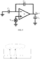
- the following explains in conjunction with FIG. 1 and a formula.
- FIG. 1 is an equivalent circuit diagram of connection between a column of fingerprint pixel circuits and a signal reading module.
- C 1 represents equivalent capacitance of a column of fingerprint pixel circuits;
- C 2 represents feedback capacitance of an operational amplifier A in the signal reading module;
- V n, eq represents equivalent noise of the operational amplifier A;
- V OUT represents a signal output end of the signal reading module.
- the larger the C 1 the larger the V OUT , noise (noise which is output by the signal reading module), which is not favorable for the signal reading module to read accurate fingerprint signals, is not favorable for manufacturing a fingerprint detection module with a larger size, and is not favorable for realizing the full-screen fingerprint detection technology.
- V OUT , noise C 1 + C 2 C 2 V n , eq
- the embodiments of the disclosure provide a fingerprint detection module, a display panel and an electronic device which are described in detail below with reference to the accompanying drawings.
- the electronic device includes, but is not limited to: a mobile phone, a tablet computer, an iPad, a digital broadcasting terminal, a messaging devices, a game console, a medical device, a fitness device, a personal digital assistant, a smart wearable device, a smart television, a sweeping robot, a smart speakers, etc.
- the electronic device includes a display panel.
- the number of the display panel is at least one, and the display panel may further include a folding screen.
- FIG. 2 is a partial cross-sectional diagram of a display panel according to an exemplary embodiment of the disclosure.
- the display panel includes a fingerprint detection module 100.
- the fingerprint detection module 100 includes an optical fingerprint detection module.
- the display panel further includes a display module 200, and the display module 200 includes a display surface.
- the fingerprint detection module 100 is disposed on the side of the display module 200 facing away from the display surface, and the orthographic projection of the fingerprint detection module 100 on the display surface entirely covers the display surface. In other words, the entire display panel may be used as a fingerprint detection region to realize the full-screen fingerprint detection technology.
- the orthographic projection of the fingerprint detection module 100 on the display surface covers a part of the display surface, so that a part of the display panel serves as a fingerprint detection region.
- the display module 200 includes an Organic Light-Emitting Diode (OLED) display layer.
- OLED Organic Light-Emitting Diode
- the display panel further includes a covering layer 300 which faces the display surface, to protect the display module 200.
- the display module 200 may emit light to the finger 400. The light is reflected by the ridges and valleys of the fingerprints of the finger 400 and is then received by the fingerprint detection module 100. The fingerprints are detected based on the light received by the fingerprint detection module 100.
- FIG. 3 is a partial schematic structural diagram of a fingerprint detection module 100 according to an exemplary embodiment of the disclosure.
- FIG. 4 is a partial schematic structural diagram of a fingerprint detection module 100 according to an exemplary embodiment of the disclosure.
- FIG. 5 is a schematic circuit diagram of column fingerprint pixel units in FIG. 4 .
- the fingerprint detection module 100 provided in some embodiments of the disclosure includes a plurality of fingerprint pixel circuits 110 and a signal reading module 120.
- the plurality of fingerprint pixel circuits 110 are arranged in multiple rows and multiple columns, that is, a fingerprint pixel circuit array is formed. Each column of fingerprint pixel circuits 110 are divided into a plurality of column fingerprint pixel units 111 along a longitudinal direction 11. Each of the plurality of column fingerprint pixel units 111 is connected to the signal reading module 120 through a respective data line 131. The signal reading module 120 is configured to read the fingerprint signals which are collected by the fingerprint pixel circuits 110.
- each of the column fingerprint pixel units 111 may include a plurality of fingerprint pixel circuits 110.
- each column of fingerprint pixel circuits 110 include three column fingerprint pixel units 111 sequentially disposed along a longitudinal direction.
- the first column of fingerprint pixel circuits 110 includes a first column fingerprint pixel unit 111-1, a second column fingerprint pixel unit 111-2 and a third column fingerprint pixel unit 111-3 which are sequentially disposed along a longitudinal direction.
- FIG. 4 Exemplarily, referring to FIG.
- each of the column fingerprint pixel units 111 includes a plurality of fingerprint pixel circuits 110, such as x fingerprint pixel circuits 110 which are sequentially a first fingerprint pixel circuit, a second fingerprint pixel circuit,..., an xth fingerprint pixel circuit along a longitudinal direction.
- x fingerprint pixel circuits 110 which are sequentially a first fingerprint pixel circuit, a second fingerprint pixel circuit,..., an xth fingerprint pixel circuit along a longitudinal direction.
- the fingerprint pixel circuit includes a passive fingerprint pixel circuit.
- the passive fingerprint pixel circuit is usually disposed on a glass substrate, which is beneficial to reducing the cost.
- the first fingerprint pixel circuit includes a gate switch Gate-1 and a photosensitive diode PD1 which are connected. When the gate switch Gate-1 is switched on, the photosensitive diode PD1 outputs the fingerprint signal converted from an optical signal to the signal reading module 120 through a data line 131.
- each column of fingerprint pixel circuits 110 are divided into a plurality of column fingerprint pixel units 111, each of the plurality of column fingerprint pixel units 111 is connected to the signal reading module 120 through a respective data line 131, and it is not that the entire column of fingerprint pixel circuits 110 are connected to the signal reading module 120 through a single data line, when the signal reading module 120 reads fingerprint signals, the load and equivalent capacitance of the fingerprint pixel circuit 110 connected to the signal reading module 120 are reduced relative to the entire column of fingerprint pixel circuits, thus reducing the noise which is output by the signal reading module 120, thereby being favorable for the signal reading module 120 to accurately read the fingerprint signals and also favorable for increasing the size of the fingerprint detection module 100 so as to realize the full-screen fingerprint detection technology.
- the fingerprint detection module 100 further includes a switch module 140, and the switch module 140 is connected between the signal reading module 120 and the column fingerprint pixel units 111.
- the switch module 140 may be controlled to switch on or switch off the column fingerprint pixel units 111 and the signal reading module 120, so as to control whether the signal reading module 120 reads the fingerprint signals which are collected by the fingerprint pixel circuits 110 in the column fingerprint pixel units 111 currently switched on.
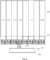
- FIG. 6 is a partial schematic structural diagram of a fingerprint detection module 100 according to an exemplary embodiment of the disclosure.
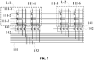
- FIG. 7 is a schematic diagram of connection between two groups of column fingerprint pixel regions 112 and switch units 141 in FIG. 6 .
- multiple columns of fingerprint pixel circuits 110 are divided into multiple groups of column fingerprint pixel regions 112 along a longitudinal direction, and each group of column fingerprint pixel region 112 includes at least two columns of fingerprint pixel circuits 110.
- the switch module 140 includes a plurality of switch units 141, and each of the switch units 141 is connected between one group of column fingerprint pixel region 112 and the signal reading module 120.
- the signal reading module 120 may read the fingerprint signal collected by the fingerprint pixel circuits 110 in the column fingerprint pixel region 112, and by further controlling other switch units 141 to be switched off to disconnect other column fingerprint pixel regions 112 and the signal reading module 120, partitioned control of the work of the fingerprint pixel circuits 110 is realized, thereby being favorable for reducing the power consumption and increasing the utilization ratio of the signal reading module 120.
- which switch units 141 are switched on may be selected based on the area of a finger pressing region, so as to realize partitioned detection of fingerprints.
- each group of column fingerprint pixel region 112 includes two columns of fingerprint pixel circuits 110.
- the column fingerprint pixel region L-1 includes a column fingerprint pixel unit 111-1 and a column fingerprint pixel unit 111-4, and other column fingerprint pixel units 111 belonging to the same column as these two columns.
- the column fingerprint pixel region L-2 includes a column fingerprint pixel unit 111-5 and a column fingerprint pixel unit 111-6, and other column fingerprint pixel units 111 belonging to the same column as these two columns.
- each of the switch units 141 includes a plurality of switches 142, and each of the switches 142 is connected to a column fingerprint pixel unit 111.
- each group of column fingerprint pixel region 112 includes two columns of fingerprint pixel circuits 110, each column of fingerprint pixel circuits 110 include three column fingerprint pixel units 111, each of the switch units 141 includes six switches 142, and each of the switches 142 is connected to a column fingerprint pixel unit 111.
- the column fingerprint pixel region L-1 includes two columns of fingerprint pixel circuits, wherein the fingerprint pixel circuit 110 of the left column includes a column fingerprint pixel unit 111-1, a column fingerprint pixel unit 111-2 and a column fingerprint pixel unit 111-3.
- each of the plurality of column fingerprint pixel units 111 is connected to the signal reading module 120 through a respective data line 131, the signal reading module 120 needs to be provided with a plurality of interfaces and a plurality of wires, which is not favorable for reducing the cost and increasing the integration level of the fingerprint detection module 100.
- at least two switch units 141 are connected to the signal reading module 120 through the same first common wires 150, thereby being favorable for reducing the number of the interfaces of the signal reading module 120 and the number of the arranged wires, so as to reduce the cost and increase the integration level of the fingerprint detection module 100.
- the first common wires 150 include a plurality of first horizontal wires 151 and a plurality of first longitudinal wires 152.
- Each group of column fingerprint pixel region 112 is connected to a switch unit 141, each group of column fingerprint pixel region 112 includes at least two columns of fingerprint pixel circuits 110. All column fingerprint pixel units 111 in each group of column fingerprint pixel region 112 are connected to the plurality of first horizontal wires 151 through a switch unit 141.
- Each of the first horizontal wires 151 is connected to the signal reading module 120 through a first longitudinal wire 152, and at least two switch units 141 are connected to the same first horizontal wires 151.
- Such a manner is favorable for reducing the number of the first horizontal wires 151, so as to increase the integration level of the fingerprint detection module 100.
- each group of column fingerprint pixel region 112 includes two columns of fingerprint pixel circuits 110, and each column of fingerprint pixel circuits 110 include three column fingerprint pixel units 111.
- six column fingerprint pixel units 111 are connected to six first horizontal wires 151 respectively through a switch unit 141, and six first horizontal wires 151 are connected to six first longitudinal wires 152 respectively.
- both the column fingerprint pixel region L-1 and the column fingerprint pixel region L-2 are connected to the same six first horizontal wires 151.
- multiple groups of column fingerprint pixel regions 112 share six first horizontal wires 151 and six first longitudinal wires 152, which is favorable for reducing the number of the wires and increasing the integration level of the fingerprint detection module 100.
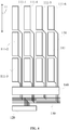
- FIG. 8 is a partial schematic structural diagram of a fingerprint detection module 100 according to an exemplary embodiment of the disclosure.
- the fingerprint detection module 100 further includes: a signal driving module 160 which is connected to each row of fingerprint pixel circuits 110 and configured to send a driving signal to each row of fingerprint pixel circuits 110, so as to drive the gate switch in each row of fingerprint pixel circuits 110 to be switched on.
- the multiple rows of fingerprint pixel circuits 110 are divided into multiple groups of row fingerprint pixel regions 113 along a horizontal direction.
- Each group of row fingerprint pixel region 113 includes a plurality of column fingerprint pixel units 111, and the plurality of column fingerprint pixel units 111 are respectively located in different columns.
- each row fingerprint pixel region 113 includes a plurality of column fingerprint pixel units 111 disposed along a horizontal direction, and in each row fingerprint pixel region 113, each column has only one column fingerprint pixel unit 111.
- the "horizontal direction” refers to a direction which is parallel to each row of fingerprint pixel circuits 110 and perpendicular to the longitudinal direction 11.
- the number of the row fingerprint pixel regions 113 is N, and from top to bottom, the row fingerprint pixel regions 113 are sequentially a row fingerprint pixel region ROWGRP-1, a row fingerprint pixel region ROWGRP-2, ..., and a row fingerprint pixel region ROWGRP-N.
- the row fingerprint pixel region ROWGRP-1 includes a plurality of column fingerprint pixel units 111.
- any group of row fingerprint pixel region 113 is driven by the signal driving module 160, and any group of column fingerprint pixel region 112 is gated by the switch module 140, so as to enable the signal reading module 120 to read the fingerprint signals of the fingerprint pixel circuits 110 in the junction regions of the row fingerprint pixel regions 113 and the column fingerprint pixel regions 112, thereby realizing partitioned detection of fingerprints, which is favorable for reducing the power consumption and increasing the utilization ratio of the signal reading module 120.
- the number of the column fingerprint pixel regions 112 is M
- the number of the row fingerprint pixel regions 113 is N.
- the signal driving module 160 and the switch module 140 cooperate to control any one of the M ⁇ N regions to output fingerprint signals, so as to realize partitioned detection of fingerprints.
- At least two groups of row fingerprint pixel regions 113 are connected to the signal driving module 160 through the same second common wires 170, thereby being favorable for reducing the number of the arranged wires and the number of the interfaces of the signal driving module 160, so as to reduce the cost of the fingerprint detection module 100 and increase the integration level of the fingerprint detection module 100.
- the second common wires 170 include a plurality of second longitudinal wires 171, and the fingerprint pixel circuits 110 in at least two groups of row fingerprint pixel regions 113 are connected to the same second longitudinal wires 171.
- each group of row fingerprint pixel region 113 includes x rows of fingerprint pixel circuits 110, the number of the second longitudinal wires 171 is x, and each row of fingerprint pixel circuits 110 in each group of row fingerprint pixel region 113 are connected to one second longitudinal wire 171.
- multiple groups of row fingerprint pixel regions 113 share x second longitudinal wires 171.
- FIG. 9 is a partial cross-sectional diagram of a fingerprint detection module 100 according to an exemplary embodiment of the disclosure.
- FIG. 10 is a partial schematic structural diagram of a fingerprint detection module 100 according to an exemplary embodiment of the disclosure.
- the fingerprint pixel circuit 110 includes fingerprint sensing units 114 and wires 130 connected in the fingerprint pixel circuits 110.
- the fingerprint sensing units 114 are disposed at a layer that is different from a layer at which the wires 130 are disposed, and the wires 130 include data lines 131.
- the data lines 131 are disposed along a longitudinal direction and are connected to the signal reading module 120. It should be noted that referring to FIG.
- the wires 130 connected in the fingerprint pixel circuits 110 further include gatelines 132 which are arranged along a horizontal direction and connected to the signal driving module 160.
- the wires 130 and the fingerprint sensing units 114 separately at different layers, the interference of the wires 130 to the fingerprint signals is reduced, and the wires 130 give way to the fingerprint sensing units 114 to avoid the occurrence of dead zones of the fingerprint detection module 100 due to a large number of wires 130, thereby being favorable for increasing the sizes of the fingerprint sensing units 114 on the premise of ensuring the resolution, further increasing the intensity of the fingerprint signals collected by the fingerprint pixel circuits 110, and being favorable for accurately detecting fingerprints.
- the fingerprint sensing unit 114 includes a photosensitive diode.
- each of the column fingerprint pixel units 111 is connected to the switch module 140 through a data line 131. Then, in the same column of fingerprint pixel circuits 110, the lengths of the data lines 131 corresponding to the plurality of column fingerprint pixel units 111 are unequal, and the number of the data lines 131 corresponding to each of the column fingerprint pixel units 111 is unequal. In this way, the environment of each of the column fingerprint pixel units 111 is inconsistent, and the generated equivalent capacitance and noise are different, so that the error of the driving signal received by each of the fingerprint pixel circuits 110 or the error of the fingerprint signal output by each of the fingerprint pixel circuits 110 is different, which is not favorable for subsequent correction and thus is not favorable for accurate fingerprint detection.
- FIG. 11 is a partial schematic structural diagram of a fingerprint detection module 100 according to an exemplary embodiment of the disclosure.
- the numbers of the wires 130 corresponding to different column fingerprint pixel units 111 are the same, and the lengths of the wires 130 corresponding to different column fingerprint pixel units 111 are the same. In this way, the environment where each of the column fingerprint pixel units 111 is located is consistent, which enables the error of the fingerprint signal collected by each of the fingerprint pixel circuits 110 to be equal, thereby facilitating subsequent correction and being favorable for accurate fingerprint detection.
- the data line 131 with a circle is a data line 131 connected to the column fingerprint pixel unit 111, and other data lines 131 are extended data lines.
- the column fingerprint pixel unit 111-1, the column fingerprint pixel unit 111-2 and the column fingerprint pixel unit 111-3 are connected to the switch module 140 respectively through a first data line 131-1, a second data line 131-2 and a third data line 131-3.
- the third data line 131-3 extends to the column fingerprint pixel unit 111-1 and the column fingerprint pixel unit 111-2, and the second data line 131-2 extends to the column fingerprint pixel unit 111-1.
- the column fingerprint pixel unit 111-1, the column fingerprint pixel unit 111-2 and the column fingerprint pixel unit 111-3 simultaneously correspond to the first data line 131-1, the second data line 131-2 and the third data line 131-3, and the first data line 131-1, second data line 131-2 and third data line 131-3 have the same length, so as to ensure that the environment where each of the column fingerprint pixel units 111 is located is consistent.
- the fingerprint detection module 100 further includes an analog-to-digital conversion module 180.
- the analog-to-digital conversion module 180 is connected to the signal reading module 120 and is configured to convert fingerprint signals into digital signals and transmit the digital signals to a control module of an electronic device, such as a Central Processing Unit (CPU), so as to facilitate the electronic device to detect fingerprints.
- CPU Central Processing Unit
- the related portions may refer to the description of the device embodiments.
- the method embodiments and the device embodiments are complementary to each other.
Landscapes
- Engineering & Computer Science (AREA)
- Theoretical Computer Science (AREA)
- Physics & Mathematics (AREA)
- Human Computer Interaction (AREA)
- General Physics & Mathematics (AREA)
- Multimedia (AREA)
- General Engineering & Computer Science (AREA)
- Microelectronics & Electronic Packaging (AREA)
- Geometry (AREA)
- Image Input (AREA)
- Measurement Of The Respiration, Hearing Ability, Form, And Blood Characteristics Of Living Organisms (AREA)
Abstract
Description
- The disclosure relates to the technical field of electronic devices, and particularly relates to a fingerprint detection module, a display panel and an electronic device.
- With the development of the full-screen technology, the under-screen fingerprint technology has become the main development trend for fingerprint detection. The under-screen fingerprint technology refers to a technology in which a fingerprint detection module of an electronic device is disposed under a display module. At present, the full-screen fingerprint detection technology of the electronic device is favored by people, and the area of the fingerprint detection module needs to be enlarged. However, this will make the load of each column of the fingerprint pixel circuits in the fingerprint detection module larger and thus generate larger noise, which is not favorable for the fingerprint detection module to obtain accurate fingerprint signals, and is not favorable for increasing the size of the fingerprint detection module.
- The disclosure provides an improved fingerprint detection module, a display panel and an electronic device.
- According to an aspect of the disclosure, there is provided a fingerprint detection module. The fingerprint detection module includes a plurality of fingerprint pixel circuits and a signal reading module.
- The plurality of fingerprint pixel circuits are arranged in multiple rows and multiple columns, each column of fingerprint pixel circuits are divided into a plurality of column fingerprint pixel units along a longitudinal direction, each of the plurality of the column fingerprint pixel units is connected to the signal reading module through a respective data line, and the signal reading module is configured to read fingerprint signals which are collected by the fingerprint pixel circuits.
- The technical solution provided by the disclosure at least has the following beneficial effects.
- Since each column of the fingerprint pixel circuits are divided into a plurality of column fingerprint pixel units, each of the plurality of column fingerprint pixel units is connected to the signal reading module through a respective data line, and it is not that the entire column of fingerprint pixel circuits are connected to the signal reading module through a data line, when the signal reading module reads fingerprint signals, the load and equivalent capacitance of the fingerprint pixel circuit connected to the signal reading module are reduced relative to the entire column of fingerprint pixel circuits, thus reducing the noise which is output by the signal reading module, thereby being favorable for the signal reading module to accurately read the fingerprint signals and also favorable for increasing the size of the fingerprint detection module so as to realize full-screen fingerprint detection.
- Optionally, the fingerprint detection module further includes a switch module, and the switch module is connected between the signal reading module and the column fingerprint pixel units.
- Optionally, the multiple columns of fingerprint pixel circuits are divided into multiple groups of column fingerprint pixel regions along a longitudinal direction, and each group of column fingerprint pixel region includes at least two columns of fingerprint pixel circuits.
- The switch module includes a plurality of switch units, and each switch unit is connected between one group of column fingerprint pixel region and the signal reading module.
- Optionally, at least two switch units are connected to the signal reading module through a same first common wires.
- Optionally, the fingerprint detection module may further include: a signal driving module which is connected to each row of fingerprint pixel circuits and configured to send a driving signal to each row of fingerprint pixel circuits.
- The multiple rows of fingerprint pixel circuits are divided into multiple groups of row fingerprint pixel regions along a horizontal direction, each group of row fingerprint pixel region includes a plurality of column fingerprint pixel units, and the plurality of column fingerprint pixel units are respectively located in different columns.
- Optionally, at least two groups of row fingerprint pixel regions are connected to the signal driving module through a same second common wires.
- Optionally, the fingerprint pixel circuit includes fingerprint sensing units and wires connected in the fingerprint pixel circuits, wherein the fingerprint sensing units are disposed at a layer that is different from a layer at which the wires are disposed.
- Optionally, numbers of the wires corresponding to different column fingerprint pixel units are the same, and lengths of the wires corresponding to different column fingerprint pixel units are the same.
- Optionally, a fingerprint pixel circuit includes a passive fingerprint pixel circuit.
- According to another aspect of the disclosure, there is provided a display panel. The display panel includes any one of the fingerprint detection modules mentioned above.
- Optionally, the display panel may further include a display module, and the display module includes a display surface.
- The fingerprint detection module is disposed on a side of the display module facing away from the display surface, and an orthographic projection of the fingerprint detection module on the display surface entirely covers the display surface.
- According to another aspect of the disclosure, there is provided an electronic device, and the electronic device includes any one of the display panels mentioned above.
-
-
FIG. 1 is an equivalent circuit diagram of connection between a column of fingerprint pixel circuits and a signal reading module. -
FIG. 2 is a partial cross-sectional diagram of a display panel according to an exemplary embodiment of the disclosure. -
FIG. 3 is a partial schematic structural diagram of a fingerprint detection module according to an exemplary embodiment of the disclosure. -
FIG. 4 is a partial schematic structural diagram of a fingerprint detection module according to an exemplary embodiment of the disclosure. -
FIG. 5 is a schematic circuit diagram of column fingerprint pixel units inFIG. 4 . -
FIG. 6 is a partial schematic structural diagram of a fingerprint detection module according to an exemplary embodiment of the disclosure. -
FIG. 7 is a schematic diagram of connection between two groups of column fingerprint pixel regions and switch units inFIG. 6 . -
FIG. 8 is a partial schematic structural diagram of a fingerprint detection module according to an exemplary embodiment of the disclosure. -
FIG. 9 is a partial cross-sectional diagram of a fingerprint detection module according to an exemplary embodiment of the disclosure. -
FIG. 10 is a partial schematic structural diagram of a fingerprint detection module according to an exemplary embodiment of the disclosure. -
FIG. 11 is a partial schematic structural diagram of a fingerprint detection module according to an exemplary embodiment of the disclosure. - Exemplary embodiments will be described in detail herein, examples of which are illustrated in the accompanying drawings. When the following description refers to the accompanying drawings, the same numbers in different drawings represent the same or similar elements unless otherwise indicated. The implementations described in the following exemplary embodiments do not represent all implementations consistent with the disclosure. Rather, they are merely examples of apparatuses and methods consistent with some aspects of the disclosure as detailed in the appended claims.
- The terms used in the disclosure are for the purpose of describing the specific embodiments only and are not intended to limit the disclosure. Unless otherwise defined, technical terms or scientific terms used in the disclosure should be understood in the ordinary meaning of those of ordinary skill in the art to which the disclosure pertains. The words "first", "second" and similar terms used in the specification and claims of the disclosure are not intended to indicate any order, quantity or importance, but only to distinguish different components. Similarly, similar words such as "one" or "a/an" do not indicate any quantity limitation, but the existence of at least one. Unless otherwise specified, similar words "comprise" or "include" and the like mean that elements or objects preceding "comprise" or "include" encompass listed elements or objects following "comprise" or "include" and their equivalents, and do not exclude other elements or objects. Words such as "connect" or "connected" are not limited to physical or mechanical connections, and may include electrical connections, whether direct or indirect.
- "A/an", "the" and "this" in a singular form in the specification of the disclosure and the appended claims are also intended to include a plural form, unless other meanings are clearly denoted throughout the disclosure. It should also be understood that the term "and/or" as used herein refers to and includes any or all possible combinations of one or more associated listed items.
- In some embodiments, the fingerprint detection module is an optical fingerprint detection module. The fingerprint detection module includes a plurality of fingerprint pixel circuits, a signal driving module and a signal reading module. The plurality of fingerprint pixel circuits are arranged in multiple rows and multiple columns, that is, a fingerprint pixel circuit array is formed. The signal driving module is configured to sequentially drive gate switches in each row of fingerprint pixel circuits to be switched on. The signal reading module is configured to read the fingerprint signal collected by the fingerprint pixel circuits, which are driven and switched on by the signal driving module, in each column of fingerprint pixel circuits.
- With the development of the full-screen fingerprint detection technology, the size of the fingerprint detection module is getting larger and larger. In other words, the area of the fingerprint pixel circuit array is getting larger and larger. This makes each column of fingerprint pixel circuits have a larger number of fingerprint pixel circuits, and each column of fingerprint pixel circuits have larger load and equivalent capacitance C 1, which is more likely to generate noise. The following explains in conjunction with
FIG. 1 and a formula. -
FIG. 1 is an equivalent circuit diagram of connection between a column of fingerprint pixel circuits and a signal reading module. C 1 represents equivalent capacitance of a column of fingerprint pixel circuits; C 2 represents feedback capacitance of an operational amplifier A in the signal reading module; V n,eq represents equivalent noise of the operational amplifier A; and V OUT represents a signal output end of the signal reading module. According to the following formula, the larger the C 1, the larger the V OUT,noise (noise which is output by the signal reading module), which is not favorable for the signal reading module to read accurate fingerprint signals, is not favorable for manufacturing a fingerprint detection module with a larger size, and is not favorable for realizing the full-screen fingerprint detection technology.
- Based on the above defects, the embodiments of the disclosure provide a fingerprint detection module, a display panel and an electronic device which are described in detail below with reference to the accompanying drawings.
- In the embodiments of the disclosure, the electronic device includes, but is not limited to: a mobile phone, a tablet computer, an iPad, a digital broadcasting terminal, a messaging devices, a game console, a medical device, a fitness device, a personal digital assistant, a smart wearable device, a smart television, a sweeping robot, a smart speakers, etc.
- In some embodiments, the electronic device includes a display panel. The number of the display panel is at least one, and the display panel may further include a folding screen.
-
FIG. 2 is a partial cross-sectional diagram of a display panel according to an exemplary embodiment of the disclosure. Referring toFIG. 2 , the display panel includes a fingerprint detection module 100. Exemplarily, the fingerprint detection module 100 includes an optical fingerprint detection module. - In some embodiments, still referring to
FIG. 2 , the display panel further includes a display module 200, and the display module 200 includes a display surface. The fingerprint detection module 100 is disposed on the side of the display module 200 facing away from the display surface, and the orthographic projection of the fingerprint detection module 100 on the display surface entirely covers the display surface. In other words, the entire display panel may be used as a fingerprint detection region to realize the full-screen fingerprint detection technology. In some other embodiments, the orthographic projection of the fingerprint detection module 100 on the display surface covers a part of the display surface, so that a part of the display panel serves as a fingerprint detection region. - Exemplarily, the display module 200 includes an Organic Light-Emitting Diode (OLED) display layer.
- In some embodiments, still referring to
FIG. 2 , the display panel further includes a covering layer 300 which faces the display surface, to protect the display module 200. When a finger 400 presses the covering layer 300, the display module 200 may emit light to the finger 400. The light is reflected by the ridges and valleys of the fingerprints of the finger 400 and is then received by the fingerprint detection module 100. The fingerprints are detected based on the light received by the fingerprint detection module 100. -
FIG. 3 is a partial schematic structural diagram of a fingerprint detection module 100 according to an exemplary embodiment of the disclosure.FIG. 4 is a partial schematic structural diagram of a fingerprint detection module 100 according to an exemplary embodiment of the disclosure.FIG. 5 is a schematic circuit diagram of column fingerprint pixel units inFIG. 4 . Referring toFIG. 3 to FIG. 5 , the fingerprint detection module 100 provided in some embodiments of the disclosure includes a plurality offingerprint pixel circuits 110 and asignal reading module 120. - The plurality of
fingerprint pixel circuits 110 are arranged in multiple rows and multiple columns, that is, a fingerprint pixel circuit array is formed. Each column offingerprint pixel circuits 110 are divided into a plurality of columnfingerprint pixel units 111 along alongitudinal direction 11. Each of the plurality of columnfingerprint pixel units 111 is connected to thesignal reading module 120 through arespective data line 131. Thesignal reading module 120 is configured to read the fingerprint signals which are collected by thefingerprint pixel circuits 110. - It should be noted that the "longitudinal direction" involved in the disclosure refers to a direction which is parallel to each column of
fingerprint pixel circuits 110 as indicated inFIG. 4 . Each of the columnfingerprint pixel units 111 may include a plurality offingerprint pixel circuits 110. - In order to more clearly understand the relationship among each column of
fingerprint pixel circuits 110, the columnfingerprint pixel units 111 and thesignal reading module 120, exemplarily, referring toFIG. 4 , each column offingerprint pixel circuits 110 include three columnfingerprint pixel units 111 sequentially disposed along a longitudinal direction. Taking the first column offingerprint pixel circuits 110 as an example, the first column offingerprint pixel circuits 110 includes a first column fingerprint pixel unit 111-1, a second column fingerprint pixel unit 111-2 and a third column fingerprint pixel unit 111-3 which are sequentially disposed along a longitudinal direction. Exemplarily, referring toFIG. 5 , each of the columnfingerprint pixel units 111 includes a plurality offingerprint pixel circuits 110, such as xfingerprint pixel circuits 110 which are sequentially a first fingerprint pixel circuit, a second fingerprint pixel circuit,..., an xth fingerprint pixel circuit along a longitudinal direction. - In some embodiments, the fingerprint pixel circuit includes a passive fingerprint pixel circuit. The passive fingerprint pixel circuit is usually disposed on a glass substrate, which is beneficial to reducing the cost. Taking the first fingerprint pixel circuit as an example, the first fingerprint pixel circuit includes a gate switch Gate-1 and a photosensitive diode PD1 which are connected. When the gate switch Gate-1 is switched on, the photosensitive diode PD1 outputs the fingerprint signal converted from an optical signal to the
signal reading module 120 through adata line 131. - Based on the above, in the fingerprint detection module 100 provided by the embodiments of the disclosure, since each column of
fingerprint pixel circuits 110 are divided into a plurality of columnfingerprint pixel units 111, each of the plurality of columnfingerprint pixel units 111 is connected to thesignal reading module 120 through arespective data line 131, and it is not that the entire column offingerprint pixel circuits 110 are connected to thesignal reading module 120 through a single data line, when thesignal reading module 120 reads fingerprint signals, the load and equivalent capacitance of thefingerprint pixel circuit 110 connected to thesignal reading module 120 are reduced relative to the entire column of fingerprint pixel circuits, thus reducing the noise which is output by thesignal reading module 120, thereby being favorable for thesignal reading module 120 to accurately read the fingerprint signals and also favorable for increasing the size of the fingerprint detection module 100 so as to realize the full-screen fingerprint detection technology. - In some embodiments, still referring to
FIG. 4 , the fingerprint detection module 100 further includes aswitch module 140, and theswitch module 140 is connected between thesignal reading module 120 and the columnfingerprint pixel units 111. Thus, theswitch module 140 may be controlled to switch on or switch off the columnfingerprint pixel units 111 and thesignal reading module 120, so as to control whether thesignal reading module 120 reads the fingerprint signals which are collected by thefingerprint pixel circuits 110 in the columnfingerprint pixel units 111 currently switched on. -
FIG. 6 is a partial schematic structural diagram of a fingerprint detection module 100 according to an exemplary embodiment of the disclosure.FIG. 7 is a schematic diagram of connection between two groups of columnfingerprint pixel regions 112 and switchunits 141 inFIG. 6 . In some embodiments, referring toFIG. 6 andFIG. 7 , multiple columns offingerprint pixel circuits 110 are divided into multiple groups of columnfingerprint pixel regions 112 along a longitudinal direction, and each group of columnfingerprint pixel region 112 includes at least two columns offingerprint pixel circuits 110. Theswitch module 140 includes a plurality ofswitch units 141, and each of theswitch units 141 is connected between one group of columnfingerprint pixel region 112 and thesignal reading module 120. In this way, by controlling at least oneswitch unit 141 to be switched on, thesignal reading module 120 may read the fingerprint signal collected by thefingerprint pixel circuits 110 in the columnfingerprint pixel region 112, and by further controllingother switch units 141 to be switched off to disconnect other columnfingerprint pixel regions 112 and thesignal reading module 120, partitioned control of the work of thefingerprint pixel circuits 110 is realized, thereby being favorable for reducing the power consumption and increasing the utilization ratio of thesignal reading module 120. Exemplarily, which switchunits 141 are switched on may be selected based on the area of a finger pressing region, so as to realize partitioned detection of fingerprints. - Still referring to
FIG. 6 , the number of the columnfingerprint pixel regions 112 is M, and from left to right, the column fingerprint pixel regions are sequentially a column fingerprint pixel region L-1, a column fingerprint pixel region L-2, a column fingerprint pixel region L-3, a column fingerprint pixel region L-4, ..., and a column fingerprint pixel region L-M. Exemplarily, each group of columnfingerprint pixel region 112 includes two columns offingerprint pixel circuits 110. For example, referring toFIG. 4 andFIG. 7 , the column fingerprint pixel region L-1 includes a column fingerprint pixel unit 111-1 and a column fingerprint pixel unit 111-4, and other columnfingerprint pixel units 111 belonging to the same column as these two columns. The column fingerprint pixel region L-2 includes a column fingerprint pixel unit 111-5 and a column fingerprint pixel unit 111-6, and other columnfingerprint pixel units 111 belonging to the same column as these two columns. - Exemplarily, referring to
FIG. 7 , each of theswitch units 141 includes a plurality ofswitches 142, and each of theswitches 142 is connected to a columnfingerprint pixel unit 111. Exemplarily, referring toFIG. 7 , each group of columnfingerprint pixel region 112 includes two columns offingerprint pixel circuits 110, each column offingerprint pixel circuits 110 include three columnfingerprint pixel units 111, each of theswitch units 141 includes sixswitches 142, and each of theswitches 142 is connected to a columnfingerprint pixel unit 111. Taking the column fingerprint pixel region L-1 as an example, the column fingerprint pixel region L-1 includes two columns of fingerprint pixel circuits, wherein thefingerprint pixel circuit 110 of the left column includes a column fingerprint pixel unit 111-1, a column fingerprint pixel unit 111-2 and a column fingerprint pixel unit 111-3. - Based on the above, since each of the plurality of column
fingerprint pixel units 111 is connected to thesignal reading module 120 through arespective data line 131, thesignal reading module 120 needs to be provided with a plurality of interfaces and a plurality of wires, which is not favorable for reducing the cost and increasing the integration level of the fingerprint detection module 100. In some embodiments, referring toFIG. 6 andFIG. 7 , at least twoswitch units 141 are connected to thesignal reading module 120 through the same firstcommon wires 150, thereby being favorable for reducing the number of the interfaces of thesignal reading module 120 and the number of the arranged wires, so as to reduce the cost and increase the integration level of the fingerprint detection module 100. - Exemplarily, referring to
FIG. 6 andFIG. 7 , the firstcommon wires 150 include a plurality of firsthorizontal wires 151 and a plurality of firstlongitudinal wires 152. Each group of columnfingerprint pixel region 112 is connected to aswitch unit 141, each group of columnfingerprint pixel region 112 includes at least two columns offingerprint pixel circuits 110. All columnfingerprint pixel units 111 in each group of columnfingerprint pixel region 112 are connected to the plurality of firsthorizontal wires 151 through aswitch unit 141. Each of the firsthorizontal wires 151 is connected to thesignal reading module 120 through a firstlongitudinal wire 152, and at least twoswitch units 141 are connected to the same firsthorizontal wires 151. Such a manner is favorable for reducing the number of the firsthorizontal wires 151, so as to increase the integration level of the fingerprint detection module 100. - Exemplarily, still referring to
FIG. 6 andFIG. 7 , the number of the firsthorizontal wires 151 is six, and the number of the firstlongitudinal wires 152 is six. Each group of columnfingerprint pixel region 112 includes two columns offingerprint pixel circuits 110, and each column offingerprint pixel circuits 110 include three columnfingerprint pixel units 111. In each group of columnfingerprint pixel region 112, six columnfingerprint pixel units 111 are connected to six firsthorizontal wires 151 respectively through aswitch unit 141, and six firsthorizontal wires 151 are connected to six firstlongitudinal wires 152 respectively. For example, both the column fingerprint pixel region L-1 and the column fingerprint pixel region L-2 are connected to the same six firsthorizontal wires 151. Thus, multiple groups of columnfingerprint pixel regions 112 share six firsthorizontal wires 151 and six firstlongitudinal wires 152, which is favorable for reducing the number of the wires and increasing the integration level of the fingerprint detection module 100. -
FIG. 8 is a partial schematic structural diagram of a fingerprint detection module 100 according to an exemplary embodiment of the disclosure. In some embodiments, referring toFIG. 3 andFIG. 8 , the fingerprint detection module 100 further includes: asignal driving module 160 which is connected to each row offingerprint pixel circuits 110 and configured to send a driving signal to each row offingerprint pixel circuits 110, so as to drive the gate switch in each row offingerprint pixel circuits 110 to be switched on. The multiple rows offingerprint pixel circuits 110 are divided into multiple groups of rowfingerprint pixel regions 113 along a horizontal direction. Each group of rowfingerprint pixel region 113 includes a plurality of columnfingerprint pixel units 111, and the plurality of columnfingerprint pixel units 111 are respectively located in different columns. In other words, each rowfingerprint pixel region 113 includes a plurality of columnfingerprint pixel units 111 disposed along a horizontal direction, and in each rowfingerprint pixel region 113, each column has only one columnfingerprint pixel unit 111. It should be noted that the "horizontal direction" refers to a direction which is parallel to each row offingerprint pixel circuits 110 and perpendicular to thelongitudinal direction 11. - Exemplarily, still referring to
FIG. 8 , the number of the rowfingerprint pixel regions 113 is N, and from top to bottom, the rowfingerprint pixel regions 113 are sequentially a row fingerprint pixel region ROWGRP-1, a row fingerprint pixel region ROWGRP-2, ..., and a row fingerprint pixel region ROWGRP-N. Taking the row fingerprint pixel region ROWGRP-1 as an example, the row fingerprint pixel region ROWGRP-1 includes a plurality of columnfingerprint pixel units 111. In this way, any group of rowfingerprint pixel region 113 is driven by thesignal driving module 160, and any group of columnfingerprint pixel region 112 is gated by theswitch module 140, so as to enable thesignal reading module 120 to read the fingerprint signals of thefingerprint pixel circuits 110 in the junction regions of the rowfingerprint pixel regions 113 and the columnfingerprint pixel regions 112, thereby realizing partitioned detection of fingerprints, which is favorable for reducing the power consumption and increasing the utilization ratio of thesignal reading module 120. - Exemplarily, the number of the column
fingerprint pixel regions 112 is M, and the number of the rowfingerprint pixel regions 113 is N. Thus, thesignal driving module 160 and theswitch module 140 cooperate to control any one of the M×N regions to output fingerprint signals, so as to realize partitioned detection of fingerprints. - In some embodiments, at least two groups of row
fingerprint pixel regions 113 are connected to thesignal driving module 160 through the same secondcommon wires 170, thereby being favorable for reducing the number of the arranged wires and the number of the interfaces of thesignal driving module 160, so as to reduce the cost of the fingerprint detection module 100 and increase the integration level of the fingerprint detection module 100. - Exemplarily, the second
common wires 170 include a plurality of secondlongitudinal wires 171, and thefingerprint pixel circuits 110 in at least two groups of rowfingerprint pixel regions 113 are connected to the same secondlongitudinal wires 171. - Exemplarily, still referring to
FIG. 8 , each group of rowfingerprint pixel region 113 includes x rows offingerprint pixel circuits 110, the number of the secondlongitudinal wires 171 is x, and each row offingerprint pixel circuits 110 in each group of rowfingerprint pixel region 113 are connected to one secondlongitudinal wire 171. Thus, multiple groups of rowfingerprint pixel regions 113 share x secondlongitudinal wires 171. -
FIG. 9 is a partial cross-sectional diagram of a fingerprint detection module 100 according to an exemplary embodiment of the disclosure.FIG. 10 is a partial schematic structural diagram of a fingerprint detection module 100 according to an exemplary embodiment of the disclosure. In some embodiments, referring toFIG. 3 ,FIG. 9 andFIG. 10 , thefingerprint pixel circuit 110 includes fingerprint sensing units 114 and wires 130 connected in thefingerprint pixel circuits 110. The fingerprint sensing units 114 are disposed at a layer that is different from a layer at which the wires 130 are disposed, and the wires 130 include data lines 131. The data lines 131 are disposed along a longitudinal direction and are connected to thesignal reading module 120. It should be noted that referring toFIG. 3 , the wires 130 connected in thefingerprint pixel circuits 110 further includegatelines 132 which are arranged along a horizontal direction and connected to thesignal driving module 160. In this way, by disposing the wires 130 and the fingerprint sensing units 114 separately at different layers, the interference of the wires 130 to the fingerprint signals is reduced, and the wires 130 give way to the fingerprint sensing units 114 to avoid the occurrence of dead zones of the fingerprint detection module 100 due to a large number of wires 130, thereby being favorable for increasing the sizes of the fingerprint sensing units 114 on the premise of ensuring the resolution, further increasing the intensity of the fingerprint signals collected by thefingerprint pixel circuits 110, and being favorable for accurately detecting fingerprints. Exemplarily, the fingerprint sensing unit 114 includes a photosensitive diode. - Referring to
FIG. 10 , each of the columnfingerprint pixel units 111 is connected to theswitch module 140 through adata line 131. Then, in the same column offingerprint pixel circuits 110, the lengths of thedata lines 131 corresponding to the plurality of columnfingerprint pixel units 111 are unequal, and the number of thedata lines 131 corresponding to each of the columnfingerprint pixel units 111 is unequal. In this way, the environment of each of the columnfingerprint pixel units 111 is inconsistent, and the generated equivalent capacitance and noise are different, so that the error of the driving signal received by each of thefingerprint pixel circuits 110 or the error of the fingerprint signal output by each of thefingerprint pixel circuits 110 is different, which is not favorable for subsequent correction and thus is not favorable for accurate fingerprint detection. -
FIG. 11 is a partial schematic structural diagram of a fingerprint detection module 100 according to an exemplary embodiment of the disclosure. In some embodiments, referring toFIG. 11 , the numbers of the wires 130 corresponding to different columnfingerprint pixel units 111 are the same, and the lengths of the wires 130 corresponding to different columnfingerprint pixel units 111 are the same. In this way, the environment where each of the columnfingerprint pixel units 111 is located is consistent, which enables the error of the fingerprint signal collected by each of thefingerprint pixel circuits 110 to be equal, thereby facilitating subsequent correction and being favorable for accurate fingerprint detection. - Exemplarily, still referring to
FIG. 11 , taking the left column offingerprint pixel circuits 110 as an example, it is sequentially divided into a column fingerprint pixel unit 111-1, a column fingerprint pixel unit 111-2 and a column fingerprint pixel unit 111-3 from top to bottom. InFIG. 11 , thedata line 131 with a circle is adata line 131 connected to the columnfingerprint pixel unit 111, andother data lines 131 are extended data lines. Specifically, the column fingerprint pixel unit 111-1, the column fingerprint pixel unit 111-2 and the column fingerprint pixel unit 111-3 are connected to theswitch module 140 respectively through a first data line 131-1, a second data line 131-2 and a third data line 131-3. The third data line 131-3 extends to the column fingerprint pixel unit 111-1 and the column fingerprint pixel unit 111-2, and the second data line 131-2 extends to the column fingerprint pixel unit 111-1. Thus, the column fingerprint pixel unit 111-1, the column fingerprint pixel unit 111-2 and the column fingerprint pixel unit 111-3 simultaneously correspond to the first data line 131-1, the second data line 131-2 and the third data line 131-3, and the first data line 131-1, second data line 131-2 and third data line 131-3 have the same length, so as to ensure that the environment where each of the columnfingerprint pixel units 111 is located is consistent. - In the embodiments of the disclosure, still referring to
FIG. 3 , the fingerprint detection module 100 further includes an analog-to-digital conversion module 180. The analog-to-digital conversion module 180 is connected to thesignal reading module 120 and is configured to convert fingerprint signals into digital signals and transmit the digital signals to a control module of an electronic device, such as a Central Processing Unit (CPU), so as to facilitate the electronic device to detect fingerprints. - Since the method embodiments basically correspond to the device embodiments, the related portions may refer to the description of the device embodiments. The method embodiments and the device embodiments are complementary to each other.
- The above embodiments of the disclosure may complement each other without causing conflicts.
- The above descriptions are only the preferred embodiments of the disclosure and are not intended to limit the disclosure.
Claims (15)
- A fingerprint detection module (100), characterized in that the fingerprint detection module (100) comprises a plurality of fingerprint pixel circuits (110) and a signal reading module (120);
wherein the plurality of fingerprint pixel circuits (110) are arranged in multiple rows and multiple columns, each column of fingerprint pixel circuits (110) are divided into a plurality of column fingerprint pixel units (111) along a longitudinal direction (11), each of the plurality of column fingerprint pixel units (111) is connected to the signal reading module (120) through a respective data line (131), and the signal reading module (120) is configured to read fingerprint signals which are collected by the fingerprint pixel circuits (110). - The fingerprint detection module (100) of claim 1, wherein the fingerprint detection module (100) further comprises a switch module (140), and the switch module (140) is connected between the signal reading module (120) and the column fingerprint pixel units (111).
- The fingerprint detection module (100) of claim 2, wherein the multiple columns of fingerprint pixel circuits (110) are divided into multiple groups of column fingerprint pixel regions (112) along the longitudinal direction (11), and each group of column fingerprint pixel region (112) comprises at least two columns of fingerprint pixel circuits (110); and
wherein the switch module (140) comprises a plurality of switch units (141), and each switch unit (141) is connected between one group of column fingerprint pixel region (112) and the signal reading module (120). - The fingerprint detection module (100) of claim 3, wherein at least two switch units (141) are connected to the signal reading module (120) through a same first common wires (150).
- The fingerprint detection module (100) of any of claims 1 to 4, wherein the fingerprint detection module (100) further comprises: a signal driving module (160) which is connected to each row of fingerprint pixel circuits (110) and configured to send a driving signal to each row of fingerprint pixel circuits (110); and
wherein the multiple rows of fingerprint pixel circuits (110) are divided into multiple groups of row fingerprint pixel regions (113) along a horizontal direction, each group of row fingerprint pixel region (113) comprises a plurality of column fingerprint pixel units (111), and the plurality of column fingerprint pixel units (111) are respectively located in different columns. - The fingerprint detection module (100) of claim 5, wherein at least two groups of row fingerprint pixel regions (113) are connected to the signal driving module (160) through a same second common wires (170).
- The fingerprint detection module (100) of any of claims 1 to 6, wherein the fingerprint pixel circuit (110) comprises fingerprint sensing units (114) and wires (130) connected in the fingerprint pixel circuits (110), and wherein the fingerprint sensing units (114) are disposed at a layer that is different from a layer at which the wires (130) are disposed, and the wires (130) comprise data lines (131).
- The fingerprint detection module (100) of claim 7, wherein numbers of the wires corresponding to different column fingerprint pixel units are the same, and lengths of the wires corresponding to different column fingerprint pixel units are the same.
- The fingerprint detection module (100) of any one of claims 1 to 8, wherein a fingerprint pixel circuit comprises a passive fingerprint pixel circuit.
- A display panel, characterized in that the display panel comprises the fingerprint detection module (100), and the fingerprint detection module (100) comprises a plurality of fingerprint pixel circuits (110) and a signal reading module (120);
wherein the plurality of fingerprint pixel circuits (110) are arranged in multiple rows and multiple columns, each column of fingerprint pixel circuits (110) are divided into a plurality of column fingerprint pixel units (111) along a longitudinal direction (11), each of the plurality of column fingerprint pixel units (111) is connected to the signal reading module (120) through a respective data line (131), and the signal reading module (120) is configured to read fingerprint signals which are collected by the fingerprint pixel circuits (110). - The display panel of claim 10, wherein the fingerprint detection module (100) further comprises a switch module (140), and the switch module (140) is connected between the signal reading module (120) and the column fingerprint pixel units (111).
- The display panel of claim 10 or 11, wherein the fingerprint detection module (100) further comprises: a signal driving module (160) which is connected to each row of fingerprint pixel circuits (110) and configured to send a driving signal to each row of fingerprint pixel circuits (110); and
wherein the multiple rows of fingerprint pixel circuits (110) are divided into multiple groups of row fingerprint pixel regions (113) along a horizontal direction, each group of row fingerprint pixel region (113) comprises a plurality of column fingerprint pixel units (111), and the plurality of column fingerprint pixel units (111) are respectively located in different columns. - The display panel of any of claims 10 to 12, wherein the fingerprint pixel circuit (110) comprises fingerprint sensing units (114) and wires (130) connected in the fingerprint pixel circuits (110), and wherein the fingerprint sensing units (114) are disposed at a layer that is different from a layer at which the wires (130) are disposed, and the wires (130) comprise data lines (131).
- The display panel of any of claims 10 to 13, wherein the display panel further comprises a display module (200), and the display module (200) comprises a display surface; and
wherein the fingerprint detection module (100) is disposed on a side of the display module (200) facing away from the display surface, and an orthographic projection of the fingerprint detection module (100) on the display surface entirely covers the display surface. - An electronic device, wherein the electronic device comprises the display panel of any one of claims 10-14.
Applications Claiming Priority (1)
| Application Number | Priority Date | Filing Date | Title |
|---|---|---|---|
| CN202010453928.0A CN113723148B (en) | 2020-05-26 | 2020-05-26 | Fingerprint detection module, display panel and electronic equipment |
Publications (1)
| Publication Number | Publication Date |
|---|---|
| EP3916624A1 true EP3916624A1 (en) | 2021-12-01 |
Family
ID=73497547
Family Applications (1)
| Application Number | Title | Priority Date | Filing Date |
|---|---|---|---|
| EP20208558.5A Pending EP3916624A1 (en) | 2020-05-26 | 2020-11-19 | Fingerprint detection module, display panel and electronic device |
Country Status (3)
| Country | Link |
|---|---|
| US (1) | US11450134B2 (en) |
| EP (1) | EP3916624A1 (en) |
| CN (1) | CN113723148B (en) |
Families Citing this family (5)
| Publication number | Priority date | Publication date | Assignee | Title |
|---|---|---|---|---|
| US11519801B1 (en) * | 2021-06-04 | 2022-12-06 | Synaptics Incorporated | Sensor device for transcapacitive sensing with shielding |
| US11816919B2 (en) | 2021-06-04 | 2023-11-14 | Synaptics Incorporated | Sensor device for transcapacitive sensing with shielding |
| CN117007617A (en) * | 2022-04-27 | 2023-11-07 | 北京京东方光电科技有限公司 | Flat panel detector, its driving method and X-ray detection device |
| CN115768198B (en) * | 2022-11-10 | 2024-09-06 | 昆山国显光电有限公司 | Display panel and display device |
| CN116110085A (en) * | 2023-01-06 | 2023-05-12 | 北京集创北方科技股份有限公司 | Capacitive sensing unit drive device, capacitive fingerprint drive chip and electronic equipment |
Citations (3)
| Publication number | Priority date | Publication date | Assignee | Title |
|---|---|---|---|---|
| EP2963918A1 (en) * | 2013-02-27 | 2016-01-06 | Sony Corporation | Solid-state imaging device, driving method, and electronic device |
| US20170097702A1 (en) * | 2015-10-01 | 2017-04-06 | Bidirectional Display, Inc. | Optical-capacitive sensor panel device and method for manufacturing same |
| US20190004663A1 (en) * | 2017-06-29 | 2019-01-03 | Wuhan China Star Optoelectronics Technology Co., Ltd. | Touch display panel and touch display device |
Family Cites Families (21)
| Publication number | Priority date | Publication date | Assignee | Title |
|---|---|---|---|---|
| CN105608406B (en) * | 2014-11-20 | 2019-05-28 | 上海箩箕技术有限公司 | Fingerprint sensor |
| CN104881196B (en) * | 2015-06-23 | 2018-04-20 | 京东方科技集团股份有限公司 | Substrate and display screen |
| CN105184247B (en) * | 2015-08-28 | 2018-12-28 | 京东方科技集团股份有限公司 | A kind of fingerprint recognition element, its recognition methods, display device and display device |
| CN106845322B (en) * | 2015-12-03 | 2020-03-10 | 上海箩箕技术有限公司 | Fingerprint imaging sensor and fingerprint imaging module that touch was awaken up |
| CN107135359B (en) * | 2016-02-26 | 2020-04-14 | 上海箩箕技术有限公司 | Image acquisition method of TFT flat-panel image sensor |
| CN105930827B (en) * | 2016-05-16 | 2019-03-01 | 京东方科技集团股份有限公司 | Array substrate, display device and driving method thereof |
| TWI622935B (en) * | 2016-07-20 | 2018-05-01 | 速博思股份有限公司 | Fingerprint identification device for eliminating interference |
| CN106874892B (en) * | 2017-03-22 | 2020-12-18 | 联想(北京)有限公司 | Fingerprint detection method and electronic equipment |
| KR101882617B1 (en) * | 2017-06-14 | 2018-07-26 | 한양대학교 산학협력단 | Capacitive in-cell touch panel structures and their readout methods |
| CN107346195B (en) * | 2017-06-29 | 2020-05-05 | 武汉华星光电技术有限公司 | Touch display panel and touch display device |
| US10755070B2 (en) * | 2017-12-12 | 2020-08-25 | Silicon Display Technology | Sensor pixel, fingerprint and image sensor including the same, and driving method thereof |
| CN209281372U (en) * | 2017-12-27 | 2019-08-20 | 深圳信炜科技有限公司 | Electronic equipment |
| CN108805044B (en) * | 2018-05-25 | 2021-03-16 | 京东方科技集团股份有限公司 | Display screen, array substrate thereof, fingerprint identification method and electronic equipment |
| TWI711953B (en) * | 2018-06-11 | 2020-12-01 | 鴻海精密工業股份有限公司 | Array substrate, display panel and display device using same |
| WO2020132913A1 (en) * | 2018-12-26 | 2020-07-02 | 深圳市汇顶科技股份有限公司 | Fingerprint recognition device and fingerprint recognition method |
| CN109934137B (en) * | 2019-02-28 | 2021-01-08 | 维沃移动通信有限公司 | Photoelectric fingerprint identification device, terminal and fingerprint identification method |
| CN110263750B (en) * | 2019-06-27 | 2021-07-30 | 厦门天马微电子有限公司 | Display panel and display device |
| CN112215215B (en) * | 2019-07-12 | 2025-01-03 | 群创光电股份有限公司 | Electronic Devices |
| WO2021042396A1 (en) * | 2019-09-06 | 2021-03-11 | 深圳市汇顶科技股份有限公司 | Fingerprint recognition apparatus and electronic device |
| CN111027498B (en) * | 2019-12-17 | 2023-04-25 | 上海思立微电子科技有限公司 | Fingerprint identification sensor and fingerprint identification method |
| CN110991396B (en) * | 2019-12-17 | 2022-10-14 | 厦门天马微电子有限公司 | Display panel, display device and fingerprint identification method |
-
2020
- 2020-05-26 CN CN202010453928.0A patent/CN113723148B/en active Active
- 2020-11-16 US US17/099,703 patent/US11450134B2/en active Active
- 2020-11-19 EP EP20208558.5A patent/EP3916624A1/en active Pending
Patent Citations (3)
| Publication number | Priority date | Publication date | Assignee | Title |
|---|---|---|---|---|
| EP2963918A1 (en) * | 2013-02-27 | 2016-01-06 | Sony Corporation | Solid-state imaging device, driving method, and electronic device |
| US20170097702A1 (en) * | 2015-10-01 | 2017-04-06 | Bidirectional Display, Inc. | Optical-capacitive sensor panel device and method for manufacturing same |
| US20190004663A1 (en) * | 2017-06-29 | 2019-01-03 | Wuhan China Star Optoelectronics Technology Co., Ltd. | Touch display panel and touch display device |
Also Published As
| Publication number | Publication date |
|---|---|
| US20210374377A1 (en) | 2021-12-02 |
| CN113723148B (en) | 2025-07-29 |
| CN113723148A (en) | 2021-11-30 |
| US11450134B2 (en) | 2022-09-20 |
Similar Documents
| Publication | Publication Date | Title |
|---|---|---|
| EP3916624A1 (en) | Fingerprint detection module, display panel and electronic device | |
| CN107346152B (en) | Display device, display screen and terminal | |
| CN109521605B (en) | Backlight module and display device | |
| US10083336B2 (en) | Fingerprint sensor integrated type touch screen panel | |
| CN110163058B (en) | Fingerprint identification display module and fingerprint identification method | |
| US10453897B2 (en) | OLED display substrate, touch display panel and display device | |
| CN107425041B (en) | touch display panel, device and manufacturing method | |
| CN112418125B (en) | Display panel, display device and control method thereof | |
| EP3748530B1 (en) | Fingerprint identification method and device, display panel and readable storage medium | |
| US20160350571A1 (en) | Fingerprint sensor integrated type touch screen panel | |
| CN107958178B (en) | Photoelectric sensor module and preparation method thereof, and electronic device | |
| TW201502917A (en) | Touch screen panel, touch sensing controller, and touch sensing system including the same | |
| CN112379790B (en) | Driving method and driving circuit of touch display panel and touch display device | |
| US11726622B2 (en) | Display device for detecting incident light | |
| CN107958179B (en) | Photoelectric sensing modules and electronic devices | |
| CN110991396B (en) | Display panel, display device and fingerprint identification method | |
| TWI621985B (en) | Capacitive fingerprint sensing apparatus | |
| CN111652188B (en) | Photosensitive sensors, optical fingerprint sensors and electronic devices made by TFT technology | |
| US11194428B2 (en) | Touch screen, pressure-sensitive touch method, and display apparatus | |
| JP2023135979A (en) | optical sensor | |
| JP2023030471A (en) | Detection device | |
| CN212135462U (en) | Photosensitive sensor, optical fingerprint sensor and electronic equipment manufactured by TFT (thin film transistor) process | |
| CN116798082B (en) | Fingerprint recognition device and its control method | |
| CN114943991B (en) | Readout chip, identification module, and identification method of TFT optical fingerprint sensor chip | |
| CN112307841B (en) | Compensation chip, screen adapter board, electronic equipment and data processing method |
Legal Events
| Date | Code | Title | Description |
|---|---|---|---|
| PUAI | Public reference made under article 153(3) epc to a published international application that has entered the european phase |
Free format text: ORIGINAL CODE: 0009012 |
|
| STAA | Information on the status of an ep patent application or granted ep patent |
Free format text: STATUS: THE APPLICATION HAS BEEN PUBLISHED |
|
| AK | Designated contracting states |
Kind code of ref document: A1 Designated state(s): AL AT BE BG CH CY CZ DE DK EE ES FI FR GB GR HR HU IE IS IT LI LT LU LV MC MK MT NL NO PL PT RO RS SE SI SK SM TR |
|
| B565 | Issuance of search results under rule 164(2) epc |
Effective date: 20210511 |
|
| STAA | Information on the status of an ep patent application or granted ep patent |
Free format text: STATUS: REQUEST FOR EXAMINATION WAS MADE |
|
| 17P | Request for examination filed |
Effective date: 20220531 |
|
| RBV | Designated contracting states (corrected) |
Designated state(s): AL AT BE BG CH CY CZ DE DK EE ES FI FR GB GR HR HU IE IS IT LI LT LU LV MC MK MT NL NO PL PT RO RS SE SI SK SM TR |
|
| STAA | Information on the status of an ep patent application or granted ep patent |
Free format text: STATUS: EXAMINATION IS IN PROGRESS |
|
| 17Q | First examination report despatched |
Effective date: 20230825 |
|
| REG | Reference to a national code |
Ref country code: DE Ref legal event code: R079 Free format text: PREVIOUS MAIN CLASS: G06K0009000000 Ipc: G06V0040130000 |
|
| GRAP | Despatch of communication of intention to grant a patent |
Free format text: ORIGINAL CODE: EPIDOSNIGR1 |
|
| STAA | Information on the status of an ep patent application or granted ep patent |
Free format text: STATUS: GRANT OF PATENT IS INTENDED |
|
| GRAJ | Information related to disapproval of communication of intention to grant by the applicant or resumption of examination proceedings by the epo deleted |
Free format text: ORIGINAL CODE: EPIDOSDIGR1 |
|
| STAA | Information on the status of an ep patent application or granted ep patent |
Free format text: STATUS: EXAMINATION IS IN PROGRESS |
|
| GRAP | Despatch of communication of intention to grant a patent |
Free format text: ORIGINAL CODE: EPIDOSNIGR1 |
|
| STAA | Information on the status of an ep patent application or granted ep patent |
Free format text: STATUS: GRANT OF PATENT IS INTENDED |
|
| RIC1 | Information provided on ipc code assigned before grant |
Ipc: G06V 40/13 20220101AFI20260119BHEP |
|
| INTG | Intention to grant announced |
Effective date: 20260129 |
|
| INTG | Intention to grant announced |
Effective date: 20260217 |