EP3916344A1 - Projection of patterned and flood illumination - Google Patents
Projection of patterned and flood illumination Download PDFInfo
- Publication number
- EP3916344A1 EP3916344A1 EP21169425.2A EP21169425A EP3916344A1 EP 3916344 A1 EP3916344 A1 EP 3916344A1 EP 21169425 A EP21169425 A EP 21169425A EP 3916344 A1 EP3916344 A1 EP 3916344A1
- Authority
- EP
- European Patent Office
- Prior art keywords
- heat sink
- target region
- platform
- optical beams
- optoelectronic apparatus
- Prior art date
- Legal status (The legal status is an assumption and is not a legal conclusion. Google has not performed a legal analysis and makes no representation as to the accuracy of the status listed.)
- Granted
Links
Images




Classifications
-
- G—PHYSICS
- G01—MEASURING; TESTING
- G01B—MEASURING LENGTH, THICKNESS OR SIMILAR LINEAR DIMENSIONS; MEASURING ANGLES; MEASURING AREAS; MEASURING IRREGULARITIES OF SURFACES OR CONTOURS
- G01B11/00—Measuring arrangements characterised by the use of optical techniques
- G01B11/24—Measuring arrangements characterised by the use of optical techniques for measuring contours or curvatures
- G01B11/25—Measuring arrangements characterised by the use of optical techniques for measuring contours or curvatures by projecting a pattern, e.g. one or more lines, moiré fringes on the object
- G01B11/2513—Measuring arrangements characterised by the use of optical techniques for measuring contours or curvatures by projecting a pattern, e.g. one or more lines, moiré fringes on the object with several lines being projected in more than one direction, e.g. grids, patterns
-
- H—ELECTRICITY
- H01—ELECTRIC ELEMENTS
- H01S—DEVICES USING THE PROCESS OF LIGHT AMPLIFICATION BY STIMULATED EMISSION OF RADIATION [LASER] TO AMPLIFY OR GENERATE LIGHT; DEVICES USING STIMULATED EMISSION OF ELECTROMAGNETIC RADIATION IN WAVE RANGES OTHER THAN OPTICAL
- H01S5/00—Semiconductor lasers
- H01S5/02—Structural details or components not essential to laser action
- H01S5/024—Arrangements for thermal management
- H01S5/02469—Passive cooling, e.g. where heat is removed by the housing as a whole or by a heat pipe without any active cooling element like a TEC
-
- H—ELECTRICITY
- H01—ELECTRIC ELEMENTS
- H01S—DEVICES USING THE PROCESS OF LIGHT AMPLIFICATION BY STIMULATED EMISSION OF RADIATION [LASER] TO AMPLIFY OR GENERATE LIGHT; DEVICES USING STIMULATED EMISSION OF ELECTROMAGNETIC RADIATION IN WAVE RANGES OTHER THAN OPTICAL
- H01S5/00—Semiconductor lasers
- H01S5/40—Arrangement of two or more semiconductor lasers, not provided for in groups H01S5/02 - H01S5/30
- H01S5/42—Arrays of surface emitting lasers
- H01S5/423—Arrays of surface emitting lasers having a vertical cavity
-
- G—PHYSICS
- G01—MEASURING; TESTING
- G01B—MEASURING LENGTH, THICKNESS OR SIMILAR LINEAR DIMENSIONS; MEASURING ANGLES; MEASURING AREAS; MEASURING IRREGULARITIES OF SURFACES OR CONTOURS
- G01B11/00—Measuring arrangements characterised by the use of optical techniques
- G01B11/24—Measuring arrangements characterised by the use of optical techniques for measuring contours or curvatures
- G01B11/25—Measuring arrangements characterised by the use of optical techniques for measuring contours or curvatures by projecting a pattern, e.g. one or more lines, moiré fringes on the object
- G01B11/254—Projection of a pattern, viewing through a pattern, e.g. moiré
-
- H—ELECTRICITY
- H01—ELECTRIC ELEMENTS
- H01S—DEVICES USING THE PROCESS OF LIGHT AMPLIFICATION BY STIMULATED EMISSION OF RADIATION [LASER] TO AMPLIFY OR GENERATE LIGHT; DEVICES USING STIMULATED EMISSION OF ELECTROMAGNETIC RADIATION IN WAVE RANGES OTHER THAN OPTICAL
- H01S5/00—Semiconductor lasers
- H01S5/005—Optical components external to the laser cavity, specially adapted therefor, e.g. for homogenisation or merging of the beams or for manipulating laser pulses, e.g. pulse shaping
- H01S5/0071—Optical components external to the laser cavity, specially adapted therefor, e.g. for homogenisation or merging of the beams or for manipulating laser pulses, e.g. pulse shaping for beam steering, e.g. using a mirror outside the cavity to change the beam direction
-
- H—ELECTRICITY
- H01—ELECTRIC ELEMENTS
- H01S—DEVICES USING THE PROCESS OF LIGHT AMPLIFICATION BY STIMULATED EMISSION OF RADIATION [LASER] TO AMPLIFY OR GENERATE LIGHT; DEVICES USING STIMULATED EMISSION OF ELECTROMAGNETIC RADIATION IN WAVE RANGES OTHER THAN OPTICAL
- H01S5/00—Semiconductor lasers
- H01S5/02—Structural details or components not essential to laser action
- H01S5/024—Arrangements for thermal management
- H01S5/02476—Heat spreaders, i.e. improving heat flow between laser chip and heat dissipating elements
-
- H—ELECTRICITY
- H01—ELECTRIC ELEMENTS
- H01S—DEVICES USING THE PROCESS OF LIGHT AMPLIFICATION BY STIMULATED EMISSION OF RADIATION [LASER] TO AMPLIFY OR GENERATE LIGHT; DEVICES USING STIMULATED EMISSION OF ELECTROMAGNETIC RADIATION IN WAVE RANGES OTHER THAN OPTICAL
- H01S5/00—Semiconductor lasers
- H01S5/02—Structural details or components not essential to laser action
- H01S5/022—Mountings; Housings
- H01S5/0225—Out-coupling of light
- H01S5/02253—Out-coupling of light using lenses
Definitions
- the present invention relates generally to optoelectronic devices, and particularly to sources of optical radiation.
- portable computing devices such as smartphones, augmented reality (AR) devices, virtual reality (VR) devices, smart watches, and smart glasses, comprise compact sources of optical radiation.
- AR augmented reality
- VR virtual reality
- portable devices comprise compact sources of optical radiation.
- optical rays optical radiation
- light refer generally to any and all of visible, infrared, and ultraviolet radiation.
- one source may emit flood radiation, illuminating a target region with a broad and uniform illumination for the purpose of feature illumination and recognition.
- Another source may, for example, project patterned radiation so as to illuminate the target region with a pattern of dots for three-dimensional (3D) mapping of the region.
- Effective heat dissipation is one of the major challenges in design of high-power optoelectronic emitters, such as vertical-cavity surface-emitting lasers (VCSELs).
- VCSELs vertical-cavity surface-emitting lasers
- Such devices generate large amounts of heat in the emitter active regions, resulting in high emitter junction temperatures, which tend to reduce VCSEL efficiency and lead to a reduced optical power output at a given drive current, shift the emission wavelength, degrade the quality of the laser modes, and reduce operating lifetime and reliability.
- inefficient heat dissipation causes temperature non-uniformity among emitters, leading to variations in emitter optical power and wavelength across the array.
- U.S. Patent 9,735,539 whose disclosure is incorporated herein by reference, describes an optoelectronic device, which includes a semiconductor substrate, having front and back sides and having at least one cavity extending from the back side through the semiconductor substrate into proximity with the front side. At least one optoelectronic emitter is formed on the front side of the semiconductor substrate in proximity with the at least one cavity. A heat-conducting material at least partially fills the at least one cavity and is configured to serve as a heat sink for the at least one optoelectronic emitter.
- Embodiments of the present invention that are described hereinbelow provide improved designs and methods of fabrication of sources of optical radiation.
- optoelectronic apparatus including a heat sink, which is shaped to define a base, a first platform at a first elevation above the base, and a second platform alongside the first platform at a second elevation above the base, which is different from the first elevation.
- a first monolithic emitter array is mounted on the first platform and is configured to emit first optical beams.
- a second monolithic emitter array is mounted on the second platform and is configured to emit second optical beams.
- An optical element is configured to direct both the first and the second optical beams toward a target region.
- the heat sink includes a metal. Additionally or alternatively, the heat sink includes a ceramic material. In a disclosed embodiment, the heat sink includes a central portion having greater thermal conductivity than a peripheral portion surrounding the central portion.
- the heat sink includes a unitary piece of material, which is shaped to define the base and the first and second platforms.
- the heat sink includes a first piece of heat sink material, which is shaped to define the base, and a second piece of heat sink material, which is mounted on the first piece of heat sink material and defines the second platform.
- the first and second monolithic emitter arrays respectively include first and second semiconductor substrates and first and second pluralities of vertical-cavity surface-emitting lasers (VCSELs) disposed respectively on the first and second semiconductor substrates.
- VCSELs vertical-cavity surface-emitting lasers
- the heat sink is positioned relative to the optical element so that the first monolithic emitter array is located at a rear focal plane of the optical element, while the second monolithic emitter array is displaced axially from the rear focal plane.
- the optical element is configured to focus the first optical beams so as to project patterned radiation onto the target region and to defocus the second optical beams so as to project flood radiation onto the target region.
- the optical element is configured to focus the first optical beams so as to project first patterned radiation onto the target region with a first focal quality and to defocus the second optical beams so as to project second patterned radiation onto the target region with a second focal quality, different from the first focal quality.
- the first optical beams are projected toward the target region with a first divergence
- the second optical beams are projected toward the target region with a second divergence, greater than the first divergence.
- a method for depth mapping which includes projecting a first pattern of radiation, with a first divergence, onto a target region and projecting a second pattern of radiation, with a second divergence, different from the first divergence, onto the target region. Respective first and second images are captured of the first and second patterns projected onto the target region. Depth coordinates of points in the target region are computed responsively to respective displacements of the first and second patterns in the first and second images and to a defocus of the second pattern relative to the first pattern in the first and second images.
- projecting the first and second patterns includes applying an optical element to direct toward the target region beams of the radiation that are emitted respectively by first and second emitter arrays, which are mounted at different locations relative to a rear focal plane of the optical element.
- the first and second patterns include spots of the radiation
- computing the depth coordinates includes comparing respective sizes of the spots in the first and second patterns in order to compute the defocus.
- a method for fabricating optoelectronic apparatus includes shaping a heat sink to define a base, a first platform at a first elevation above the base, and a second platform alongside the first platform at a second elevation above the base, which is different from the first elevation.
- a first monolithic emitter array, which is configured to emit first optical beams, is mounted on the first platform, and a second monolithic emitter array, which is configured to emit second optical beams, is mounted on the second platform.
- An optical element is positioned to direct both the first and the second optical beams toward a target region.
- radiation sources of different focal qualities are combined into a single optoelectronic apparatus comprising an optical element, such as a lens, and two monolithic emitter arrays, both of which emit optical beams through the optical element.
- One of the arrays is positioned at the rear focal plane of the optical element, while the other array is displaced from the rear focal plane, for example by axial shift of 100 ⁇ m or more.
- the beams emitted by the array at the rear focal plane are projected by the element as collimated beams, thus projecting patterned radiation on a target region in a pattern corresponding to the layout of the emitters in the array.
- the beams emitted by the array that is displaced from the rear focal plane are defocused.
- the monolithic arrays comprise arrays of vertical-cavity surface-emitting lasers (VCSELs), disposed on semiconductor substrates, such as a gallium-arsenide (GaAs) substrate; but alternatively, other types of emitters may be used.
- VCSELs vertical-cavity surface-emitting lasers
- GaAs gallium-arsenide
- the position of the defocused array is chosen depending on the desired degree of defocus.
- the defocus is sufficient so that the projected beams create a broad and largely uniform field of flood illumination.
- the defocus is chosen so that the beams projected from the defocused array also create patterned radiation.
- the apparatus thus projects two different patterns, with pattern elements (such as spots) whose sizes vary differently as a function of distance from the apparatus.
- Positioning the two arrays precisely within the required range of distances from the optical element can be difficult. This difficulty is exacerbated by the need to sink away the substantial amount of heat that is generated by the emitters.
- Embodiments of the present invention that are described herein address these problems by providing a heat sink, which is shaped to define two platforms at different elevations above the base of the heat sink.
- the two monolithic arrays of emitters are mounted respectively on the two platforms, thus positioning the two arrays at different elevations.
- the heat sink may be fabricated from a metal, such as copper (Cu) or copper-tungsten alloy (CuW), or from a ceramic material, such as aluminum nitride (AlN), or other suitable materials with a high thermal conductivity.
- a metal such as copper (Cu) or copper-tungsten alloy (CuW)
- a ceramic material such as aluminum nitride (AlN)
- AlN aluminum nitride
- Thermal gradients of the VCSEL arrays may be compensated in the heat sink by fabricating it from a composite material, such as Cu/CuW, or by opening vias in the heat sink, as described, for example, in the above-mentioned U.S. Patent 9,735,539 .
- Fig. 1 is a schematic sectional view of an optoelectronic apparatus 20, in accordance with an embodiment of the invention.
- Optoelectronic apparatus 20 comprises a heat sink 22 comprising a unitary piece of material, which is shaped to define a base 24 and first and second platforms 26 and 28, respectively, wherein the first platform is above the base by an elevation E 1 , and the second platform is above the base by an elevation E 2 , and wherein E 1 ⁇ E 2 .
- Heat sink 22 may be fabricated from a metal, such as copper (Cu) or copper-tungsten alloy (CuW), or from a ceramic material, such as aluminum nitride (AlN), as these materials have a high thermal conductivity.
- a metal such as copper (Cu) or copper-tungsten alloy (CuW)
- AlN aluminum nitride
- VCSEL arrays 30 and 32 are mounted on respective platforms 26 and 28.
- Apparatus 20 further comprises an optical element 34 with a rear focal plane 36.
- Heat sink 22 is positioned relative to optical element 34 so that VCSEL array 30 is located at rear focal plane 36, while array 32 is displaced axially from the rear focal plane by a distance ⁇ .
- Typical values for ⁇ vary, depending on the focal length of optical element 34, for example from 50 ⁇ m to 500 ⁇ m, although ⁇ may also assume values outside this range.
- Figs. 2a and 2b are schematic side views of optoelectronic apparatus 20 illuminating a target region 40 respectively with patterned radiation 42 and flood radiation 44, in accordance with an embodiment of the invention. Where applicable, labels from Fig. 1 are used for similar items in Figs. 2a and 2b .
- VCSEL array 30 is driven to emit first optical beams 46 towards optical element 34.
- beams 46 are collimated and projected by the optical element towards target region 40 as collimated beams 48.
- Beams 48 illuminate target region 40 with patterned radiation 42, comprising discrete spots 50 of radiation (with the pattern shown in an enlarged scale), in a pattern determined, for example, by the layout of the VCSELs in array 30.
- spots 50 appear in the figures to be laid out in a regular pattern, it can be advantageous for purposes of depth mapping that the arrangement of the VCSELs in array 30, and hence of spots 50, be irregular, for example laid out in a pseudorandom pattern.
- VCSEL array 32 is driven to emit second optical beams 52 towards optical element 34.
- beams 52 are defocused and projected by the optical element towards target region 40 as diverging beams 54.
- Beams 54 illuminate target region 40 with flood radiation 44, comprising blurred, overlapping spots 56, resulting in a broad and substantially uniform illumination of the target region.
- Figs. 2c and 2d are schematic side views of optoelectronic apparatus 57 illuminating target region 40 respectively with patterned radiation 42 and 59 of different focal qualities, in accordance with an alternative embodiment of the invention.
- the components of apparatus 57 are similar to those of apparatus 20, and the same indicator numbers are used to refer to the same components in Figs. 2c-d as in Figs. 2a-b .
- the displacement of VCSEL array 32 from rear focal plane 36 is chosen so that beams 54 form distinct spots 58 on target region 40.
- the displacement of VCSEL array 32 from rear focal plane 36 is relatively smaller than in apparatus 20.
- spots 58 are typically larger than spots 50 and have larger divergence, i.e., spots 58 grow more rapidly as a function of distance from apparatus 57 than do spots 50.
- the difference in spot size and the divergence can be set by appropriate choice of the displacement of VCSEL array 32 from rear focal plane 36, as well as adjusting other optical parameters of apparatus 57. For example, in a miniaturized device of short focal length, displacement of VCSEL array 32 by as little as 20 ⁇ m from rear focal plane 36 can result in a difference of 50% in the far-field size of spots 58 relative to spots 50.
- the combination of two different patterns of radiation 42 and 59 with different divergences can be helpful in enhancing the accuracy of depth mapping using apparatus 57. This feature of the apparatus is described further hereinbelow with reference to Fig. 9 .
- Fig. 3 is a schematic sectional view of a heat sink 60, in accordance with another embodiment of the invention. Where applicable, labels from Figs. 1-2 are used for similar items in Fig. 3 .
- Heat sink 60 is similar to heat sink 22 in Figs. 1-2 , but whereas heat sink 22 comprises a unitary piece, heat sink 60 comprises a first piece 62 of heat sink material, which is shaped to define base 24 and first platform 26, and a second piece 64 of heat sink material, which is mounted on the first piece and defines second platform 28.
- First and second pieces 62 and 64 may be fabricated from the same material, as described above, or from two different materials.
- first piece 62 may be fabricated from AlN
- second piece 64 may be fabricated from Cu.
- Fig. 4 is a schematic sectional view of a heat sink 70, in accordance with yet another embodiment of the invention. Where applicable, labels from Figs. 1-2 are used for similar items in Fig. 4 .
- Heat sink 70 is similar to heat sink 22, but whereas in heat sink 22 second platform 28 is built up above base 24, in heat sink 70 first platform 26 is contained within a cavity, which may be machined or etched down into the material of the heat sink, for example.
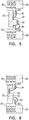
- Fig. 5 is a schematic sectional of heat sink 22 and VSEL arrays 30 and 32 ( Fig. 1 ) mounted on a ceramic mount 80, in accordance with an embodiment of the invention. Where applicable, labels from Figs. 1-2 are used for similar items in Fig. 5 .
- Heat sink 22 is mounted on ceramic mount 80 and attached to it by, for example, suitable cement.
- Ceramic mount 80 comprises electrical conductors 82, fabricated for example from gold (Au).
- VCSEL arrays 30 and 32 are coupled to conductors 82 by wire bonds 84.
- Fig. 6 is a schematic sectional view of heat sink 70 ( Fig. 4 ) and VCSEL arrays 30 and 32 mounted on a ceramic mount 90, in accordance with another embodiment of the invention. Where applicable, labels from Figs. 1-4 are used for similar items in Fig. 6 .
- heat sink 70 is mounted on ceramic mount 90 and attached to it by, for example, suitable cement.
- Ceramic mount 90 comprises, similarly to ceramic mount 80, electrical conductors 92 fabricated from Au.
- VCSEL arrays 30 and 32 are coupled to conductors 92 by wire bonds 94.
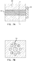
- Figs. 7a and 7b are schematic sectional views of a heat sink 100, in accordance with an embodiment of the invention.
- the features of heat sink 100 may be incorporated in heat sink 22 or in the other heat sinks described above.
- a VCSEL array 102 is mounted on heat sink 100, and together they form a part of an optoelectronic apparatus similar to apparatus 20.
- heat sink 100 and VCSEL array 102 may replace second piece 64 and VCSEL array 32 in Fig. 3 .
- Heat sink 100 is fabricated of a metal or a ceramic material, similarly to heat sink 22 ( Fig. 1 ).
- Heat sink 100 comprises vias 104, which are configured to modify the thermal conductivity of the heat sink so as to compensate for thermal gradients of VCSEL array 102.
- the VCSELs in the central region of array 102 tend to operate under a heavier heat load than those in the peripheral regions, due to heat dissipation from neighboring VCSELs.
- Vias 104 are useful in sinking heat preferentially away from the central region, so that operating temperatures are roughly equalized.
- Fig. 7b is a schematic sectional view of heat sink 100 along a section A-A of Fig. 7a .
- Vias 104 are arranged in a concentric configuration, with a central via of greater diameter than the peripheral vias, thus aiding in compensating for thermal gradients of VCSEL array 102.
- the arrangement and dimensions of vias 104 may be modified in order to accommodate different designs and thermal gradients of VCSEL array 102.
- Figs. 8a and 8b are schematic sectional views of a heat sink 120, in accordance with another embodiment of the invention. In this case, too, the features of heat sink 120 can be incorporated in heat sink 22 or in the other heat sinks described above.
- a VCSEL array 122 is mounted on heat sink 120, and together they form a part of an optoelectronic apparatus similar to apparatus 20.
- heat sink 120 and VCSEL array 122 may replace second piece 64 and VCSEL array 32 in Fig. 3 .
- Heat sink 120 is fabricated as a composite material comprising a central Cu-core 124 and a CuW-mantle 126, wherein the core has a higher thermal conductivity than the mantle, thus compensating for thermal gradients of VCSEL array 122.
- Fig. 8b is a schematic sectional view of heat sink 120 along a section B-B of Fig. 8a .
- the arrangement, dimensions, and materials of core 124 and mantle 126 may be modified in order to accommodate different designs and thermal gradients of VCSEL array 122.
- Fig. 9 is a flow chart that schematically illustrates a method for depth mapping using radiation patterns of different focal qualities, in accordance with an embodiment of the invention. This method is described hereinbelow, for the sake of clarity and concreteness, specifically with reference to patterned radiation 42 and 59, as shown in Figs. 2c-d . The principles of this embodiment may alternatively be applied using other sorts of pattern projectors with suitable capabilities.
- an image capture assembly (not shown in the figures) captures images of the patterns of spots 50 and 58 that are projected onto target region 40, from a location that is offset relative to apparatus 57 that projects the patterned radiation, as is known in the art of depth mapping using structured light.
- Apparatus 57 is actuated to project patterned radiation 42 in alternation with patterned radiation 59, by applying drive currents to the corresponding VCSEL arrays 30 and 32.
- Patterned radiation 42 and 59 respectively define different patterns on target region 40, referred to in Fig. 9 as "pattern A” and "pattern B.”
- the image capture assembly captures images of both patterns.
- the processor compares the locations of spots 50 and 58 in the images to corresponding reference patterns of the spots, and calculates two sets of depth coordinates (shown in Fig. 9 as "depth A" and "depth B") of points in the target region based on the displacement between the spots in the images and their reference locations.
- depth A depth A
- depth B depth coordinates
- the processor can improve the depth resolution still further by computing and applying the relative defocus ⁇ of spots 58 relative to spots 50.
- the processor may extract and use either the absolute sizes of spots 50 and 58 or the relative sizes, or both absolute and relative sizes, in estimating the distance to each spot in the images based on the different, known divergences of beams 48 and 54.
- the defocus gives an additional, independent measure of depth, which can be used to refine and resolve ambiguities in the displacement-based depth coordinates depth A and depth B.
Landscapes
- Physics & Mathematics (AREA)
- General Physics & Mathematics (AREA)
- Optics & Photonics (AREA)
- Condensed Matter Physics & Semiconductors (AREA)
- Electromagnetism (AREA)
- Engineering & Computer Science (AREA)
- Computer Vision & Pattern Recognition (AREA)
- Semiconductor Lasers (AREA)
Abstract
Description
- The present invention relates generally to optoelectronic devices, and particularly to sources of optical radiation.
- Various sorts of portable computing devices (referred to collectively as "portable devices" in the description), such as smartphones, augmented reality (AR) devices, virtual reality (VR) devices, smart watches, and smart glasses, comprise compact sources of optical radiation. (The terms "optical rays," "optical radiation," and "light," as used in the present description and in the claims, refer generally to any and all of visible, infrared, and ultraviolet radiation.) For example, one source may emit flood radiation, illuminating a target region with a broad and uniform illumination for the purpose of feature illumination and recognition. Another source may, for example, project patterned radiation so as to illuminate the target region with a pattern of dots for three-dimensional (3D) mapping of the region. Effective heat dissipation is one of the major challenges in design of high-power optoelectronic emitters, such as vertical-cavity surface-emitting lasers (VCSELs). Such devices generate large amounts of heat in the emitter active regions, resulting in high emitter junction temperatures, which tend to reduce VCSEL efficiency and lead to a reduced optical power output at a given drive current, shift the emission wavelength, degrade the quality of the laser modes, and reduce operating lifetime and reliability. In VCSEL array devices, inefficient heat dissipation causes temperature non-uniformity among emitters, leading to variations in emitter optical power and wavelength across the array.
- In response to this problem,
U.S. Patent 9,735,539 - Embodiments of the present invention that are described hereinbelow provide improved designs and methods of fabrication of sources of optical radiation.
- There is therefore provided, in accordance with an embodiment of the invention, optoelectronic apparatus, including a heat sink, which is shaped to define a base, a first platform at a first elevation above the base, and a second platform alongside the first platform at a second elevation above the base, which is different from the first elevation. A first monolithic emitter array is mounted on the first platform and is configured to emit first optical beams. A second monolithic emitter array is mounted on the second platform and is configured to emit second optical beams. An optical element is configured to direct both the first and the second optical beams toward a target region.
- In one embodiment, the heat sink includes a metal. Additionally or alternatively, the heat sink includes a ceramic material. In a disclosed embodiment, the heat sink includes a central portion having greater thermal conductivity than a peripheral portion surrounding the central portion.
- In some embodiments, the heat sink includes a unitary piece of material, which is shaped to define the base and the first and second platforms. Alternatively, the heat sink includes a first piece of heat sink material, which is shaped to define the base, and a second piece of heat sink material, which is mounted on the first piece of heat sink material and defines the second platform.
- In a disclosed embodiment, the first and second monolithic emitter arrays respectively include first and second semiconductor substrates and first and second pluralities of vertical-cavity surface-emitting lasers (VCSELs) disposed respectively on the first and second semiconductor substrates.
- In some embodiments, the heat sink is positioned relative to the optical element so that the first monolithic emitter array is located at a rear focal plane of the optical element, while the second monolithic emitter array is displaced axially from the rear focal plane. In one embodiment, the optical element is configured to focus the first optical beams so as to project patterned radiation onto the target region and to defocus the second optical beams so as to project flood radiation onto the target region. Alternatively, the optical element is configured to focus the first optical beams so as to project first patterned radiation onto the target region with a first focal quality and to defocus the second optical beams so as to project second patterned radiation onto the target region with a second focal quality, different from the first focal quality. In a disclosed embodiment, the first optical beams are projected toward the target region with a first divergence, and the second optical beams are projected toward the target region with a second divergence, greater than the first divergence.
- There is also provided, in accordance with an embodiment of the invention, a method for depth mapping, which includes projecting a first pattern of radiation, with a first divergence, onto a target region and projecting a second pattern of radiation, with a second divergence, different from the first divergence, onto the target region. Respective first and second images are captured of the first and second patterns projected onto the target region. Depth coordinates of points in the target region are computed responsively to respective displacements of the first and second patterns in the first and second images and to a defocus of the second pattern relative to the first pattern in the first and second images.
- In a disclosed embodiment, projecting the first and second patterns includes applying an optical element to direct toward the target region beams of the radiation that are emitted respectively by first and second emitter arrays, which are mounted at different locations relative to a rear focal plane of the optical element. Additionally or alternatively, the first and second patterns include spots of the radiation, and computing the depth coordinates includes comparing respective sizes of the spots in the first and second patterns in order to compute the defocus.
- There is additionally provided, in accordance with an embodiment of the invention, a method for fabricating optoelectronic apparatus. The method includes shaping a heat sink to define a base, a first platform at a first elevation above the base, and a second platform alongside the first platform at a second elevation above the base, which is different from the first elevation. A first monolithic emitter array, which is configured to emit first optical beams, is mounted on the first platform, and a second monolithic emitter array, which is configured to emit second optical beams, is mounted on the second platform. An optical element is positioned to direct both the first and the second optical beams toward a target region.
- The present invention will be more fully understood from the following detailed description of the embodiments thereof, taken together with the drawings in which:
-
-
Fig. 1 is a schematic sectional view of an optoelectronic apparatus, in accordance with an embodiment of the invention; -
Figs. 2a and 2b are schematic side views of optoelectronic apparatus illuminating a target region with patterned radiation and flood radiation, respectively, in accordance with an embodiment of the invention; -
Figs. 2c and 2d are schematic side views of optoelectronic apparatus illuminating a target region by patterned radiation with different focal properties, in accordance with an alternative embodiment of the invention; -
Fig. 3 is a schematic sectional view of a heat sink on which emitter arrays are mounted, in accordance with another embodiment of the invention; -
Fig. 4 is a schematic sectional view of a heat sink on which emitter arrays are mounted, in accordance with yet another embodiment of the invention; -
Fig. 5 is a schematic sectional of a heat sink and emitter arrays mounted on a ceramic mount, in accordance with an embodiment of the invention; -
Fig. 6 is a schematic sectional view of a heat sink and emitter arrays mounted on a ceramic mount, in accordance with another embodiment of the invention; -
Figs. 7a and 7b are schematic sectional views of a heat sink, in accordance with an embodiment of the invention; -
Figs. 8a and 8b are schematic sectional views of a heat sink, in accordance with another embodiment of the invention; and -
Fig. 9 is a flow chart that schematically illustrates a method for depth mapping using patterned radiation of different focal qualities, in accordance with an embodiment of the invention. - In embodiments of the present invention, radiation sources of different focal qualities are combined into a single optoelectronic apparatus comprising an optical element, such as a lens, and two monolithic emitter arrays, both of which emit optical beams through the optical element. One of the arrays is positioned at the rear focal plane of the optical element, while the other array is displaced from the rear focal plane, for example by axial shift of 100 µm or more. The beams emitted by the array at the rear focal plane are projected by the element as collimated beams, thus projecting patterned radiation on a target region in a pattern corresponding to the layout of the emitters in the array. The beams emitted by the array that is displaced from the rear focal plane are defocused. In the disclosed embodiments, the monolithic arrays comprise arrays of vertical-cavity surface-emitting lasers (VCSELs), disposed on semiconductor substrates, such as a gallium-arsenide (GaAs) substrate; but alternatively, other types of emitters may be used.
- The position of the defocused array is chosen depending on the desired degree of defocus. In some embodiments, the defocus is sufficient so that the projected beams create a broad and largely uniform field of flood illumination. In an alternative embodiment, the defocus is chosen so that the beams projected from the defocused array also create patterned radiation. The apparatus thus projects two different patterns, with pattern elements (such as spots) whose sizes vary differently as a function of distance from the apparatus.
- Positioning the two arrays precisely within the required range of distances from the optical element can be difficult. This difficulty is exacerbated by the need to sink away the substantial amount of heat that is generated by the emitters.
- Embodiments of the present invention that are described herein address these problems by providing a heat sink, which is shaped to define two platforms at different elevations above the base of the heat sink. The two monolithic arrays of emitters are mounted respectively on the two platforms, thus positioning the two arrays at different elevations.
- In the disclosed embodiments, mounting the two monolithic arrays on the two platforms provides the required differential focal distances (distances from the optical element) for the two arrays. The heat sink may be fabricated from a metal, such as copper (Cu) or copper-tungsten alloy (CuW), or from a ceramic material, such as aluminum nitride (AlN), or other suitable materials with a high thermal conductivity.
- Thermal gradients of the VCSEL arrays may be compensated in the heat sink by fabricating it from a composite material, such as Cu/CuW, or by opening vias in the heat sink, as described, for example, in the above-mentioned
U.S. Patent 9,735,539 -
Fig. 1 is a schematic sectional view of anoptoelectronic apparatus 20, in accordance with an embodiment of the invention.Optoelectronic apparatus 20 comprises aheat sink 22 comprising a unitary piece of material, which is shaped to define abase 24 and first andsecond platforms VCSEL arrays respective platforms Apparatus 20 further comprises anoptical element 34 with a rearfocal plane 36.Heat sink 22 is positioned relative tooptical element 34 so thatVCSEL array 30 is located at rearfocal plane 36, whilearray 32 is displaced axially from the rear focal plane by a distance Δ. Typical values for Δ vary, depending on the focal length ofoptical element 34, for example from 50 µm to 500 µm, although Δ may also assume values outside this range. -
Figs. 2a and 2b are schematic side views ofoptoelectronic apparatus 20 illuminating atarget region 40 respectively with patternedradiation 42 andflood radiation 44, in accordance with an embodiment of the invention. Where applicable, labels fromFig. 1 are used for similar items inFigs. 2a and 2b . - In
Fig. 2a ,VCSEL array 30 is driven to emit firstoptical beams 46 towardsoptical element 34. AsVCSEL array 30 is located at rearfocal plane 36 ofoptical element 34, beams 46 are collimated and projected by the optical element towardstarget region 40 as collimated beams 48.Beams 48 illuminatetarget region 40 with patternedradiation 42, comprisingdiscrete spots 50 of radiation (with the pattern shown in an enlarged scale), in a pattern determined, for example, by the layout of the VCSELs inarray 30. Althoughspots 50 appear in the figures to be laid out in a regular pattern, it can be advantageous for purposes of depth mapping that the arrangement of the VCSELs inarray 30, and hence ofspots 50, be irregular, for example laid out in a pseudorandom pattern. - In
Fig. 2b ,VCSEL array 32 is driven to emit secondoptical beams 52 towardsoptical element 34. AsVCSEL array 32 is displaced axially from rearfocal plane 36, beams 52 are defocused and projected by the optical element towardstarget region 40 as diverging beams 54.Beams 54 illuminatetarget region 40 withflood radiation 44, comprising blurred, overlappingspots 56, resulting in a broad and substantially uniform illumination of the target region. -
Figs. 2c and 2d are schematic side views ofoptoelectronic apparatus 57 illuminatingtarget region 40 respectively with patternedradiation apparatus 57 are similar to those ofapparatus 20, and the same indicator numbers are used to refer to the same components inFigs. 2c-d as inFigs. 2a-b . Inapparatus 57, however, the displacement ofVCSEL array 32 from rearfocal plane 36 is chosen so thatbeams 54 formdistinct spots 58 ontarget region 40. Typically, in this embodiment the displacement ofVCSEL array 32 from rearfocal plane 36 is relatively smaller than inapparatus 20. - Due to the defocus of
beams 52, spots 58 are typically larger thanspots 50 and have larger divergence, i.e., spots 58 grow more rapidly as a function of distance fromapparatus 57 than do spots 50. The difference in spot size and the divergence can be set by appropriate choice of the displacement ofVCSEL array 32 from rearfocal plane 36, as well as adjusting other optical parameters ofapparatus 57. For example, in a miniaturized device of short focal length, displacement ofVCSEL array 32 by as little as 20 µm from rearfocal plane 36 can result in a difference of 50% in the far-field size ofspots 58 relative tospots 50. The combination of two different patterns ofradiation mapping using apparatus 57. This feature of the apparatus is described further hereinbelow with reference toFig. 9 . -
Fig. 3 is a schematic sectional view of aheat sink 60, in accordance with another embodiment of the invention. Where applicable, labels fromFigs. 1-2 are used for similar items inFig. 3 . -
Heat sink 60 is similar toheat sink 22 inFigs. 1-2 , but whereasheat sink 22 comprises a unitary piece,heat sink 60 comprises afirst piece 62 of heat sink material, which is shaped to definebase 24 andfirst platform 26, and asecond piece 64 of heat sink material, which is mounted on the first piece and definessecond platform 28. First andsecond pieces first piece 62 may be fabricated from AlN, andsecond piece 64 may be fabricated from Cu. -
Fig. 4 is a schematic sectional view of aheat sink 70, in accordance with yet another embodiment of the invention. Where applicable, labels fromFigs. 1-2 are used for similar items inFig. 4 .Heat sink 70 is similar toheat sink 22, but whereas inheat sink 22second platform 28 is built up abovebase 24, inheat sink 70first platform 26 is contained within a cavity, which may be machined or etched down into the material of the heat sink, for example. -
Fig. 5 is a schematic sectional ofheat sink 22 andVSEL arrays 30 and 32 (Fig. 1 ) mounted on aceramic mount 80, in accordance with an embodiment of the invention. Where applicable, labels fromFigs. 1-2 are used for similar items inFig. 5 .Heat sink 22 is mounted onceramic mount 80 and attached to it by, for example, suitable cement.Ceramic mount 80 compriseselectrical conductors 82, fabricated for example from gold (Au).VCSEL arrays conductors 82 bywire bonds 84. -
Fig. 6 is a schematic sectional view of heat sink 70 (Fig. 4 ) andVCSEL arrays ceramic mount 90, in accordance with another embodiment of the invention. Where applicable, labels fromFigs. 1-4 are used for similar items inFig. 6 . Similarly toFig. 5 ,heat sink 70 is mounted onceramic mount 90 and attached to it by, for example, suitable cement.Ceramic mount 90 comprises, similarly toceramic mount 80,electrical conductors 92 fabricated from Au.VCSEL arrays conductors 92 bywire bonds 94. -
Figs. 7a and 7b are schematic sectional views of aheat sink 100, in accordance with an embodiment of the invention. The features ofheat sink 100 may be incorporated inheat sink 22 or in the other heat sinks described above. - In
Fig. 7a , aVCSEL array 102 is mounted onheat sink 100, and together they form a part of an optoelectronic apparatus similar toapparatus 20. For example,heat sink 100 andVCSEL array 102 may replacesecond piece 64 andVCSEL array 32 inFig. 3 .Heat sink 100 is fabricated of a metal or a ceramic material, similarly to heat sink 22 (Fig. 1 ). -
Heat sink 100 comprisesvias 104, which are configured to modify the thermal conductivity of the heat sink so as to compensate for thermal gradients ofVCSEL array 102. Specifically, the VCSELs in the central region ofarray 102 tend to operate under a heavier heat load than those in the peripheral regions, due to heat dissipation from neighboring VCSELs.Vias 104 are useful in sinking heat preferentially away from the central region, so that operating temperatures are roughly equalized. -
Fig. 7b is a schematic sectional view ofheat sink 100 along a section A-A ofFig. 7a .Vias 104 are arranged in a concentric configuration, with a central via of greater diameter than the peripheral vias, thus aiding in compensating for thermal gradients ofVCSEL array 102. The arrangement and dimensions ofvias 104 may be modified in order to accommodate different designs and thermal gradients ofVCSEL array 102. -
Figs. 8a and 8b are schematic sectional views of aheat sink 120, in accordance with another embodiment of the invention. In this case, too, the features ofheat sink 120 can be incorporated inheat sink 22 or in the other heat sinks described above. - In
Fig. 8a , aVCSEL array 122 is mounted onheat sink 120, and together they form a part of an optoelectronic apparatus similar toapparatus 20. For example,heat sink 120 andVCSEL array 122 may replacesecond piece 64 andVCSEL array 32 inFig. 3 .Heat sink 120 is fabricated as a composite material comprising a central Cu-core 124 and a CuW-mantle 126, wherein the core has a higher thermal conductivity than the mantle, thus compensating for thermal gradients ofVCSEL array 122. -
Fig. 8b is a schematic sectional view ofheat sink 120 along a section B-B ofFig. 8a . The arrangement, dimensions, and materials ofcore 124 andmantle 126 may be modified in order to accommodate different designs and thermal gradients ofVCSEL array 122. -
Fig. 9 is a flow chart that schematically illustrates a method for depth mapping using radiation patterns of different focal qualities, in accordance with an embodiment of the invention. This method is described hereinbelow, for the sake of clarity and concreteness, specifically with reference to patternedradiation Figs. 2c-d . The principles of this embodiment may alternatively be applied using other sorts of pattern projectors with suitable capabilities. The description that follows assumes that an image capture assembly (not shown in the figures) captures images of the patterns ofspots target region 40, from a location that is offset relative toapparatus 57 that projects the patterned radiation, as is known in the art of depth mapping using structured light. An arrangement of this sort, in which both the spot locations and shape characteristics are detected by an image capture assembly and analyzed by a processor in order to create a 3D map (also referred to as a depth map), is described, for example, inU.S. Patent 8,050,461 , whose disclosure is incorporated herein by reference. -
Apparatus 57 is actuated to project patternedradiation 42 in alternation with patternedradiation 59, by applying drive currents to the correspondingVCSEL arrays radiation target region 40, referred to inFig. 9 as "pattern A" and "pattern B." The image capture assembly captures images of both patterns. The processor compares the locations ofspots Fig. 9 as "depth A" and "depth B") of points in the target region based on the displacement between the spots in the images and their reference locations. The use of two different patterns thus enables the processor to find the depth coordinates with improved spatial resolution, relative to the resolution achievable using only a single projected pattern. - The processor can improve the depth resolution still further by computing and applying the relative defocus Δ of
spots 58 relative tospots 50. For this purpose, the processor may extract and use either the absolute sizes ofspots beams - It will be appreciated that the embodiments described above are cited by way of example, and that the present invention is not limited to what has been particularly shown and described hereinabove. Rather, the scope of the present invention includes both combinations and subcombinations of the various features described hereinabove, as well as variations and modifications thereof which would occur to persons skilled in the art upon reading the foregoing description and which are not disclosed in the prior art.
Claims (15)
- An optoelectronic apparatus (20, 57), comprising:a heat sink (22, 60, 70), which is shaped to define a base (24), a first platform (26) at a first elevation above the base, and a second platform (28) alongside the first platform at a second elevation above the base, which is different from the first elevation;a first monolithic emitter array (30), which is mounted on the first platform and is configured to emit first optical beams;a second monolithic emitter array (32), which is mounted on the second platform and is configured to emit second optical beams; andan optical element (34) configured to direct both the first and the second optical beams toward a target region.
- The optoelectronic apparatus according to claim 1, wherein the heat sink comprises a metal.
- The optoelectronic apparatus according to claim 1, wherein the heat sink comprises a ceramic material.
- The optoelectronic apparatus according to any preceding claim, wherein the heat sink comprises a central portion having greater thermal conductivity than a peripheral portion surrounding the central portion.
- The optoelectronic apparatus according to any preceding claim, wherein the heat sink comprises a unitary piece of material, which is shaped to define the base and the first and second platforms.
- The optoelectronic apparatus according to any preceding claim, wherein the heat sink comprises a first piece of heat sink material, which is shaped to define the base, and a second piece of heat sink material, which is mounted on the first piece of heat sink material and defines the second platform.
- The optoelectronic apparatus according to any preceding claim, wherein the first and second monolithic emitter arrays respectively comprise first and second semiconductor substrates and first and second pluralities of vertical-cavity surface-emitting lasers (VCSELs) disposed respectively on the first and second semiconductor substrates.
- The optoelectronic apparatus according to any preceding claim, wherein the heat sink is positioned relative to the optical element so that the first monolithic emitter array is located at a rear focal plane of the optical element, while the second monolithic emitter array is displaced axially from the rear focal plane.
- The optoelectronic apparatus according to claim 8, wherein the optical element is configured to focus the first optical beams so as to project patterned radiation onto the target region and to defocus the second optical beams so as to project flood radiation onto the target region.
- The optoelectronic apparatus according to claim 8, wherein the optical element is configured to focus the first optical beams so as to project first patterned radiation onto the target region with a first focal quality and to defocus the second optical beams so as to project second patterned radiation onto the target region with a second focal quality, different from the first focal quality.
- The optoelectronic apparatus according to claim 10, wherein the first optical beams are projected toward the target region with a first divergence, and the second optical beams are projected toward the target region with a second divergence, greater than the first divergence.
- A method for depth mapping, comprising:projecting a first pattern of radiation (42), with a first divergence, onto a target region;projecting a second pattern of radiation (59), with a second divergence, different from the first divergence, onto the target region;capturing respective first and second images of the first and second patterns projected onto the target region; andcomputing depth coordinates of points in the target region responsively to respective displacements of the first and second patterns in the first and second images and to a defocus of the second pattern relative to the first pattern in the first and second images.
- The method according to claim 12, wherein projecting the first and second patterns comprises applying an optical element to direct toward the target region beams of the radiation that are emitted respectively by first and second emitter arrays, which are mounted at different locations relative to a rear focal plane of the optical element.
- The method according to claim 12 or 13, wherein the first and second patterns comprise spots of the radiation, and wherein computing the depth coordinates comprises comparing respective sizes of the spots in the first and second patterns in order to compute the defocus.
- A method for fabricating optoelectronic apparatus (20, 57), comprising:shaping a heat sink (22, 60, 70) to define a base (24), a first platform (26) at a first elevation above the base, and a second platform (28) alongside the first platform at a second elevation above the base, which is different from the first elevation;mounting a first monolithic emitter array (30), which is configured to emit first optical beams, on the first platform;mounting a second monolithic emitter array (32), which is configured to emit second optical beams, on the second platform; andpositioning an optical element (34) to direct both the first and the second optical beams toward a target region.
Applications Claiming Priority (3)
| Application Number | Priority Date | Filing Date | Title |
|---|---|---|---|
| US202063029499P | 2020-05-25 | 2020-05-25 | |
| US202063105361P | 2020-10-26 | 2020-10-26 | |
| US17/223,047 US11710945B2 (en) | 2020-05-25 | 2021-04-06 | Projection of patterned and flood illumination |
Publications (2)
| Publication Number | Publication Date |
|---|---|
| EP3916344A1 true EP3916344A1 (en) | 2021-12-01 |
| EP3916344B1 EP3916344B1 (en) | 2023-11-08 |
Family
ID=75625359
Family Applications (1)
| Application Number | Title | Priority Date | Filing Date |
|---|---|---|---|
| EP21169425.2A Active EP3916344B1 (en) | 2020-05-25 | 2021-04-20 | Projection of patterned and flood illumination |
Country Status (3)
| Country | Link |
|---|---|
| US (1) | US11710945B2 (en) |
| EP (1) | EP3916344B1 (en) |
| CN (1) | CN113725722B (en) |
Families Citing this family (9)
| Publication number | Priority date | Publication date | Assignee | Title |
|---|---|---|---|---|
| CN114428437B (en) * | 2022-01-14 | 2024-05-14 | 深圳市安思疆科技有限公司 | 3D projector and electronic equipment that structured light and floodlight illumination put together |
| CN117128892A (en) * | 2022-05-18 | 2023-11-28 | 华为技术有限公司 | Three-dimensional information measurement device, measurement method and electronic equipment |
| US12474516B2 (en) * | 2022-08-04 | 2025-11-18 | Stmicroelectronics (Research & Development) Limited | Flood and dot emitter |
| US12546912B2 (en) | 2022-09-04 | 2026-02-10 | Apple Inc. | Integrated spot and flood illumination projector |
| US12313812B2 (en) | 2022-09-20 | 2025-05-27 | Apple Inc. | MOE-based illumination projector |
| US12123589B1 (en) | 2023-05-22 | 2024-10-22 | Apple Inc. | Flood projector with microlens array |
| WO2025046067A1 (en) | 2023-08-31 | 2025-03-06 | Trinamix Gmbh | Optical elements on flood vcsels for 2in1 projectors |
| WO2025046063A1 (en) | 2023-08-31 | 2025-03-06 | Trinamix Gmbh | Single vcsel combined dot and flood projector |
| EP4530666A1 (en) * | 2023-09-29 | 2025-04-02 | trinamiX GmbH | 2in1 projector with polarized vcsels and beam splitter |
Citations (6)
| Publication number | Priority date | Publication date | Assignee | Title |
|---|---|---|---|---|
| EP0949728A1 (en) * | 1998-04-10 | 1999-10-13 | Hewlett-Packard Company | A monolithic multiple wavelenght VCSEL array |
| US20080106746A1 (en) * | 2005-10-11 | 2008-05-08 | Alexander Shpunt | Depth-varying light fields for three dimensional sensing |
| US9735539B2 (en) | 2015-07-20 | 2017-08-15 | Apple Inc. | VCSEL structure with embedded heat sink |
| WO2018132521A1 (en) * | 2017-01-16 | 2018-07-19 | Canthus Technologies Llc | Combining light-emitting elements of differing divergence on the same substrate |
| US20190268068A1 (en) * | 2011-08-26 | 2019-08-29 | Trilumina Corp. | Wide-angle illuminator module |
| WO2020026616A1 (en) * | 2018-08-01 | 2020-02-06 | ソニーセミコンダクタソリューションズ株式会社 | Light source device, image sensor, and sensing module |
Family Cites Families (86)
| Publication number | Priority date | Publication date | Assignee | Title |
|---|---|---|---|---|
| US4069463A (en) | 1976-09-02 | 1978-01-17 | International Business Machines Corporation | Injection laser array |
| US4935939A (en) * | 1989-05-24 | 1990-06-19 | Liau Zong Long | Surface emitting laser with monolithic integrated lens |
| US5812571A (en) | 1996-10-25 | 1998-09-22 | W. L. Gore & Associates, Inc. | High-power vertical cavity surface emitting laser cluster |
| US6156980A (en) | 1998-06-04 | 2000-12-05 | Delco Electronics Corp. | Flip chip on circuit board with enhanced heat dissipation and method therefor |
| US6597713B2 (en) | 1998-07-22 | 2003-07-22 | Canon Kabushiki Kaisha | Apparatus with an optical functional device having a special wiring electrode and method for fabricating the same |
| WO2001088993A2 (en) | 2000-05-19 | 2001-11-22 | Mcmaster University | A METHOD FOR LOCALLY MODIFYING THE EFFECTIVE BANDGAP ENERGY IN INDIUM GALLIUM ARSENIDE PHOSPHIDE (InGaAsP) QUANTUM WELL STRUCTURES |
| US20020070443A1 (en) | 2000-12-08 | 2002-06-13 | Xiao-Chun Mu | Microelectronic package having an integrated heat sink and build-up layers |
| US6636539B2 (en) | 2001-05-25 | 2003-10-21 | Novalux, Inc. | Method and apparatus for controlling thermal variations in an optical device |
| US7126218B1 (en) | 2001-08-07 | 2006-10-24 | Amkor Technology, Inc. | Embedded heat spreader ball grid array |
| US6674948B2 (en) | 2001-08-13 | 2004-01-06 | Optoic Technology, Inc. | Optoelectronic IC module |
| US6744072B2 (en) | 2001-10-02 | 2004-06-01 | Xerox Corporation | Substrates having increased thermal conductivity for semiconductor structures |
| US7006354B2 (en) | 2001-10-26 | 2006-02-28 | Fujikura Ltd. | Heat radiating structure for electronic device |
| US6936855B1 (en) | 2002-01-16 | 2005-08-30 | Shane Harrah | Bendable high flux LED array |
| US6625028B1 (en) | 2002-06-20 | 2003-09-23 | Agilent Technologies, Inc. | Heat sink apparatus that provides electrical isolation for integrally shielded circuit |
| US6771502B2 (en) | 2002-06-28 | 2004-08-03 | Advanced Energy Technology Inc. | Heat sink made from longer and shorter graphite sheets |
| US7899339B2 (en) | 2002-07-30 | 2011-03-01 | Amplification Technologies Inc. | High-sensitivity, high-resolution detector devices and arrays |
| US7271461B2 (en) | 2004-02-27 | 2007-09-18 | Banpil Photonics | Stackable optoelectronics chip-to-chip interconnects and method of manufacturing |
| CN100555589C (en) | 2005-06-29 | 2009-10-28 | 皇家飞利浦电子股份有限公司 | Method for manufacturing semiconductor components |
| US7303005B2 (en) | 2005-11-04 | 2007-12-04 | Graftech International Holdings Inc. | Heat spreaders with vias |
| US8355117B2 (en) | 2005-12-21 | 2013-01-15 | Ecole Polytechnique Federale De Lausanne | Method and arrangement for measuring the distance to an object |
| US20070262441A1 (en) | 2006-05-09 | 2007-11-15 | Chi-Ming Chen | Heat sink structure for embedded chips and method for fabricating the same |
| WO2008087652A2 (en) | 2007-01-21 | 2008-07-24 | Prime Sense Ltd. | Depth mapping using multi-beam illumination |
| WO2008113067A2 (en) | 2007-03-15 | 2008-09-18 | Johns Hopkins University | Deep submicron and nano cmos single photon photodetector pixel with event based circuits for readout data-rate reduction |
| US8494252B2 (en) | 2007-06-19 | 2013-07-23 | Primesense Ltd. | Depth mapping using optical elements having non-uniform focal characteristics |
| US7652252B1 (en) | 2007-10-08 | 2010-01-26 | Hrl Laboratories, Llc | Electronically tunable and reconfigurable hyperspectral photon detector |
| US8026471B2 (en) | 2008-07-23 | 2011-09-27 | Princeton Lightwave, Inc. | Single-photon avalanche detector-based focal plane array |
| IT1392366B1 (en) | 2008-12-17 | 2012-02-28 | St Microelectronics Rousset | OPERATING PHOTODIODO IN GEIGER MODE WITH INTEGRATED AND CONTROLLABLE SUPPRESSION RESISTOR, PHOTODIUM RING AND RELATIVE PROCESS OF PROCESSING |
| JP5197421B2 (en) | 2009-02-17 | 2013-05-15 | 新光電気工業株式会社 | The camera module |
| US7949024B2 (en) | 2009-02-17 | 2011-05-24 | Trilumina Corporation | Multibeam arrays of optoelectronic devices for high frequency operation |
| US10038304B2 (en) | 2009-02-17 | 2018-07-31 | Trilumina Corp. | Laser arrays for variable optical properties |
| US8604603B2 (en) | 2009-02-20 | 2013-12-10 | The Hong Kong University Of Science And Technology | Apparatus having thermal-enhanced and cost-effective 3D IC integration structure with through silicon via interposers |
| CN101923173B (en) | 2009-06-10 | 2014-10-01 | 圣戈本陶瓷及塑料股份有限公司 | Scintillator and detector assembly |
| US20110026264A1 (en) | 2009-07-29 | 2011-02-03 | Reed William G | Electrically isolated heat sink for solid-state light |
| WO2011060319A1 (en) * | 2009-11-13 | 2011-05-19 | Uni-Light Llc | Led thermal management |
| US8427749B2 (en) * | 2010-06-30 | 2013-04-23 | Jds Uniphase Corporation | Beam combining light source |
| US8654811B2 (en) | 2010-08-25 | 2014-02-18 | Flir Systems, Inc. | Serially interconnected vertical-cavity surface emitting laser arrays |
| JP5930263B2 (en) | 2011-02-18 | 2016-06-08 | ソニー株式会社 | Solid-state imaging device |
| DE102011107645A1 (en) | 2011-07-12 | 2013-01-17 | Leica Microsystems Cms Gmbh | Apparatus and method for detecting light |
| RU2610339C2 (en) | 2011-10-10 | 2017-02-09 | Конинклейке Филипс Н.В. | Method of vcsel crystals mounting on crystal holder |
| US9024246B2 (en) | 2011-12-19 | 2015-05-05 | Princeton Lightwave, Inc. | Two-state negative feedback avalanche diode having a control element for determining load state |
| FR2984522B1 (en) | 2011-12-20 | 2014-02-14 | St Microelectronics Grenoble 2 | DEVICE FOR DETECTING THE PROXIMITY OF AN OBJECT, COMPRISING SPAD PHOTODIODS |
| US20130163627A1 (en) | 2011-12-24 | 2013-06-27 | Princeton Optronics | Laser Illuminator System |
| GB2498529A (en) | 2012-01-17 | 2013-07-24 | St Microelectronics Res & Dev | Image sensor comprising positive feedback between a bias line and the output of multiple ADCs |
| US9052356B2 (en) | 2012-02-15 | 2015-06-09 | International Business Machines Corporation | Embedded photon emission calibration (EPEC) |
| WO2013160789A1 (en) | 2012-04-26 | 2013-10-31 | Koninklijke Philips N.V. | Optically pumped vertical external-cavity surface-emitting laser device |
| US20130342835A1 (en) | 2012-06-25 | 2013-12-26 | California Institute Of Technology | Time resolved laser raman spectroscopy using a single photon avalanche diode array |
| WO2014087301A1 (en) * | 2012-12-05 | 2014-06-12 | Koninklijke Philips N.V. | Illumination array with adapted distribution of radiation |
| GB2510890A (en) | 2013-02-18 | 2014-08-20 | St Microelectronics Res & Dev | Method and apparatus |
| JP6383516B2 (en) | 2013-04-19 | 2018-08-29 | ライトスピン テクノロジーズ、インク. | Integrated avalanche photodiode array |
| GB2514576A (en) | 2013-05-29 | 2014-12-03 | St Microelectronics Res & Dev | Methods and apparatus |
| US9826131B2 (en) | 2013-09-23 | 2017-11-21 | Heptagon Micro Optics Pte. Ltd. | Compact camera module arrangements that facilitate dam-and-fill and similar encapsulation techniques |
| US9430006B1 (en) | 2013-09-30 | 2016-08-30 | Google Inc. | Computing device with heat spreader |
| DE102013111496A1 (en) | 2013-10-18 | 2015-04-23 | Osram Opto Semiconductors Gmbh | Method for producing optoelectronic semiconductor components and optoelectronic semiconductor component |
| US9210350B2 (en) | 2013-12-09 | 2015-12-08 | Omnivision Technologies, Inc. | Low power imaging system with single photon avalanche diode photon counters and ghost image reduction |
| US9480185B2 (en) | 2014-01-08 | 2016-10-25 | Enphase Energy, Inc. | Double insulated heat spreader |
| US9312401B2 (en) | 2014-01-15 | 2016-04-12 | Omnivision Technologies, Inc. | Single photon avalanche diode imaging sensor for complementary metal oxide semiconductor stacked chip applications |
| US9331116B2 (en) | 2014-01-15 | 2016-05-03 | Omnivision Technologies, Inc. | Back side illuminated single photon avalanche diode imaging sensor with high short wavelength detection efficiency |
| US9520696B2 (en) | 2014-03-04 | 2016-12-13 | Princeton Optronics Inc. | Processes for making reliable VCSEL devices and VCSEL arrays |
| US9668334B2 (en) | 2014-05-23 | 2017-05-30 | General Electric Company | Thermal clamp apparatus for electronic systems |
| US9355985B2 (en) | 2014-05-30 | 2016-05-31 | Freescale Semiconductor, Inc. | Microelectronic packages having sidewall-deposited heat spreader structures and methods for the fabrication thereof |
| US9819144B2 (en) | 2015-05-14 | 2017-11-14 | Apple Inc. | High-efficiency vertical emitters with improved heat sinking |
| US10034375B2 (en) | 2015-05-21 | 2018-07-24 | Apple Inc. | Circuit substrate with embedded heat sink |
| US10684444B2 (en) | 2015-08-17 | 2020-06-16 | Lg Innotek Co., Ltd. | Camera module |
| CN205123806U (en) | 2015-11-04 | 2016-03-30 | 联想(北京)有限公司 | Mobile terminal with front camera and large LCD |
| KR20190002488A (en) | 2016-04-28 | 2019-01-08 | 트리나미엑스 게엠베하 | A detector for optically detecting at least one object |
| WO2017205063A1 (en) | 2016-05-27 | 2017-11-30 | Verily Life Sciences Llc | Systems and methods for surface topography acquisition using laser speckle |
| US10225954B2 (en) | 2016-09-23 | 2019-03-05 | Apple Inc. | Thermal transfer between electronic device and case |
| US9980412B2 (en) | 2016-09-29 | 2018-05-22 | Intel Corporation | Flexible heat spreader |
| US20190324223A1 (en) | 2016-12-29 | 2019-10-24 | Intel Corporation | Photonic engine platform utilizing embedded wafer level packaging integration |
| CN107219711A (en) | 2017-06-22 | 2017-09-29 | 努比亚技术有限公司 | Camera module and mobile terminal |
| CN111034167B (en) | 2017-08-29 | 2021-12-14 | 索尼半导体解决方案公司 | Imaging device and method of manufacturing the same |
| CN108332082B (en) * | 2018-01-15 | 2020-06-30 | 深圳奥比中光科技有限公司 | Lighting module |
| DE102018102144A1 (en) | 2018-01-31 | 2019-08-01 | Tdk Electronics Ag | Electronic component |
| CN110196527A (en) | 2018-02-26 | 2019-09-03 | 光宝光电(常州)有限公司 | Miniaturization structure light projection module |
| US10600187B2 (en) * | 2018-03-20 | 2020-03-24 | Owl Autonomous Imaging, Inc. | Trajectory detection devices and methods |
| US10897122B2 (en) | 2018-04-20 | 2021-01-19 | Hewlett Packard Enterprise Development Lp | Optical apparatus for optical transceivers |
| FR3082634B1 (en) | 2018-06-18 | 2021-10-01 | Delphi Tech Llc | OPTICAL DEVICE FOR VEHICLES INCLUDING A HEATING ELEMENT |
| JP7374195B2 (en) | 2018-08-24 | 2023-11-06 | トリナミクス ゲゼルシャフト ミット ベシュレンクテル ハフツング | Detector for determining the position of at least one object |
| US11988748B2 (en) | 2018-09-24 | 2024-05-21 | Lawrence Livermore National Security, Llc | System and method for adaptable lidar imaging |
| US10551886B1 (en) | 2018-10-08 | 2020-02-04 | Google Llc | Display with integrated graphite heat spreader and printed circuit board insulator |
| DE102018125281A1 (en) | 2018-10-12 | 2020-04-16 | Osram Opto Semiconductors Gmbh | Optoelectronic semiconductor component |
| US10401480B1 (en) | 2018-12-05 | 2019-09-03 | Luminar Technologies, Inc. | Lidar receiver with multiple detectors for range-ambiguity mitigation |
| TWI704658B (en) | 2019-06-04 | 2020-09-11 | 恆勁科技股份有限公司 | Package substrate |
| US10881028B1 (en) | 2019-07-03 | 2020-12-29 | Apple Inc. | Efficient heat removal from electronic modules |
| CN210224593U (en) | 2019-07-15 | 2020-03-31 | 太平洋(聊城)光电科技股份有限公司 | High thermal conductivity metal bonding structure |
| CN110867724B (en) | 2020-01-17 | 2020-07-03 | 常州纵慧芯光半导体科技有限公司 | High-speed TOF structure and manufacturing method |
-
2021
- 2021-04-06 US US17/223,047 patent/US11710945B2/en active Active
- 2021-04-20 EP EP21169425.2A patent/EP3916344B1/en active Active
- 2021-05-14 CN CN202110528468.8A patent/CN113725722B/en active Active
Patent Citations (7)
| Publication number | Priority date | Publication date | Assignee | Title |
|---|---|---|---|---|
| EP0949728A1 (en) * | 1998-04-10 | 1999-10-13 | Hewlett-Packard Company | A monolithic multiple wavelenght VCSEL array |
| US20080106746A1 (en) * | 2005-10-11 | 2008-05-08 | Alexander Shpunt | Depth-varying light fields for three dimensional sensing |
| US8050461B2 (en) | 2005-10-11 | 2011-11-01 | Primesense Ltd. | Depth-varying light fields for three dimensional sensing |
| US20190268068A1 (en) * | 2011-08-26 | 2019-08-29 | Trilumina Corp. | Wide-angle illuminator module |
| US9735539B2 (en) | 2015-07-20 | 2017-08-15 | Apple Inc. | VCSEL structure with embedded heat sink |
| WO2018132521A1 (en) * | 2017-01-16 | 2018-07-19 | Canthus Technologies Llc | Combining light-emitting elements of differing divergence on the same substrate |
| WO2020026616A1 (en) * | 2018-08-01 | 2020-02-06 | ソニーセミコンダクタソリューションズ株式会社 | Light source device, image sensor, and sensing module |
Also Published As
| Publication number | Publication date |
|---|---|
| CN113725722B (en) | 2024-08-30 |
| US20210364902A1 (en) | 2021-11-25 |
| CN113725722A (en) | 2021-11-30 |
| EP3916344B1 (en) | 2023-11-08 |
| US11710945B2 (en) | 2023-07-25 |
Similar Documents
| Publication | Publication Date | Title |
|---|---|---|
| EP3916344B1 (en) | Projection of patterned and flood illumination | |
| US9553423B2 (en) | Miniature structured light illuminator | |
| US8000360B2 (en) | Laser diode assemblies | |
| US9869453B2 (en) | Light source, light source unit, and light source module using same | |
| US20200185877A1 (en) | Optical module | |
| US11619365B2 (en) | Light source unit, illumination device, processing equipment, and deflection element | |
| TWI825023B (en) | Light modeling device, lighting control method and lighting control program | |
| US7443895B2 (en) | Modular diode laser assembly | |
| US7586963B2 (en) | Modular diode laser assembly | |
| JP2004179607A (en) | Laser device | |
| US12519282B2 (en) | Light-emitting apparatus and manufacturing method thereof | |
| EP2908390B1 (en) | Semiconductor laser light source | |
| CN115668668A (en) | Light emitting device and distance measuring device | |
| US12107387B2 (en) | Vertical cavity surface emitting laser (VCSEL) array package and manufacturing method | |
| JPH05206578A (en) | External cavity diode laser | |
| WO2021256421A1 (en) | Semiconductor light-emitting device and light-emitting apparatus provided with same | |
| Moench et al. | VCSEL arrays with integrated optics | |
| EP1296316A1 (en) | Image recorder and light source unit | |
| US11973317B2 (en) | Semiconductor laser and projector | |
| TWI781193B (en) | Light emitting module, light source unit, light shaping device | |
| EP1353421B1 (en) | Optical module with a monitor photo diode | |
| Leers et al. | Cooling approaches for high power diode laser bars | |
| US20250030219A1 (en) | Laser component and method for producing a laser component | |
| JP2020161663A (en) | Semiconductor laser device | |
| Primerov et al. | Compact optical module with RGB superluminescent diodes and collinearly aligned collimated output beams |
Legal Events
| Date | Code | Title | Description |
|---|---|---|---|
| PUAI | Public reference made under article 153(3) epc to a published international application that has entered the european phase |
Free format text: ORIGINAL CODE: 0009012 |
|
| STAA | Information on the status of an ep patent application or granted ep patent |
Free format text: STATUS: REQUEST FOR EXAMINATION WAS MADE |
|
| 17P | Request for examination filed |
Effective date: 20210420 |
|
| AK | Designated contracting states |
Kind code of ref document: A1 Designated state(s): AL AT BE BG CH CY CZ DE DK EE ES FI FR GB GR HR HU IE IS IT LI LT LU LV MC MK MT NL NO PL PT RO RS SE SI SK SM TR |
|
| B565 | Issuance of search results under rule 164(2) epc |
Effective date: 20210924 |
|
| RIN1 | Information on inventor provided before grant (corrected) |
Inventor name: WRIGHT, CHRISTOPHER M. Inventor name: MIAO, ZHENGYU Inventor name: TSUR, YUVAL Inventor name: SVENSEN, OYVIND Inventor name: GOVINDARAJAN, HARISH Inventor name: ALNAHHAS, YAZAN |
|
| GRAP | Despatch of communication of intention to grant a patent |
Free format text: ORIGINAL CODE: EPIDOSNIGR1 |
|
| STAA | Information on the status of an ep patent application or granted ep patent |
Free format text: STATUS: GRANT OF PATENT IS INTENDED |
|
| INTG | Intention to grant announced |
Effective date: 20230713 |
|
| GRAS | Grant fee paid |
Free format text: ORIGINAL CODE: EPIDOSNIGR3 |
|
| GRAA | (expected) grant |
Free format text: ORIGINAL CODE: 0009210 |
|
| STAA | Information on the status of an ep patent application or granted ep patent |
Free format text: STATUS: THE PATENT HAS BEEN GRANTED |
|
| AK | Designated contracting states |
Kind code of ref document: B1 Designated state(s): AL AT BE BG CH CY CZ DE DK EE ES FI FR GB GR HR HU IE IS IT LI LT LU LV MC MK MT NL NO PL PT RO RS SE SI SK SM TR |
|
| REG | Reference to a national code |
Ref country code: GB Ref legal event code: FG4D |
|
| REG | Reference to a national code |
Ref country code: CH Ref legal event code: EP |
|
| REG | Reference to a national code |
Ref country code: DE Ref legal event code: R096 Ref document number: 602021006549 Country of ref document: DE |
|
| REG | Reference to a national code |
Ref country code: IE Ref legal event code: FG4D |
|
| REG | Reference to a national code |
Ref country code: LT Ref legal event code: MG9D |
|
| P01 | Opt-out of the competence of the unified patent court (upc) registered |
Effective date: 20240126 |
|
| REG | Reference to a national code |
Ref country code: NL Ref legal event code: MP Effective date: 20231108 |
|
| PG25 | Lapsed in a contracting state [announced via postgrant information from national office to epo] |
Ref country code: GR Free format text: LAPSE BECAUSE OF FAILURE TO SUBMIT A TRANSLATION OF THE DESCRIPTION OR TO PAY THE FEE WITHIN THE PRESCRIBED TIME-LIMIT Effective date: 20240209 |
|
| PG25 | Lapsed in a contracting state [announced via postgrant information from national office to epo] |
Ref country code: IS Free format text: LAPSE BECAUSE OF FAILURE TO SUBMIT A TRANSLATION OF THE DESCRIPTION OR TO PAY THE FEE WITHIN THE PRESCRIBED TIME-LIMIT Effective date: 20240308 |
|
| PG25 | Lapsed in a contracting state [announced via postgrant information from national office to epo] |
Ref country code: LT Free format text: LAPSE BECAUSE OF FAILURE TO SUBMIT A TRANSLATION OF THE DESCRIPTION OR TO PAY THE FEE WITHIN THE PRESCRIBED TIME-LIMIT Effective date: 20231108 |
|
| REG | Reference to a national code |
Ref country code: AT Ref legal event code: MK05 Ref document number: 1629951 Country of ref document: AT Kind code of ref document: T Effective date: 20231108 |
|
| PG25 | Lapsed in a contracting state [announced via postgrant information from national office to epo] |
Ref country code: NL Free format text: LAPSE BECAUSE OF FAILURE TO SUBMIT A TRANSLATION OF THE DESCRIPTION OR TO PAY THE FEE WITHIN THE PRESCRIBED TIME-LIMIT Effective date: 20231108 |
|
| PG25 | Lapsed in a contracting state [announced via postgrant information from national office to epo] |
Ref country code: AT Free format text: LAPSE BECAUSE OF FAILURE TO SUBMIT A TRANSLATION OF THE DESCRIPTION OR TO PAY THE FEE WITHIN THE PRESCRIBED TIME-LIMIT Effective date: 20231108 |
|
| PG25 | Lapsed in a contracting state [announced via postgrant information from national office to epo] |
Ref country code: ES Free format text: LAPSE BECAUSE OF FAILURE TO SUBMIT A TRANSLATION OF THE DESCRIPTION OR TO PAY THE FEE WITHIN THE PRESCRIBED TIME-LIMIT Effective date: 20231108 |
|
| PG25 | Lapsed in a contracting state [announced via postgrant information from national office to epo] |
Ref country code: NL Free format text: LAPSE BECAUSE OF FAILURE TO SUBMIT A TRANSLATION OF THE DESCRIPTION OR TO PAY THE FEE WITHIN THE PRESCRIBED TIME-LIMIT Effective date: 20231108 Ref country code: LT Free format text: LAPSE BECAUSE OF FAILURE TO SUBMIT A TRANSLATION OF THE DESCRIPTION OR TO PAY THE FEE WITHIN THE PRESCRIBED TIME-LIMIT Effective date: 20231108 Ref country code: IS Free format text: LAPSE BECAUSE OF FAILURE TO SUBMIT A TRANSLATION OF THE DESCRIPTION OR TO PAY THE FEE WITHIN THE PRESCRIBED TIME-LIMIT Effective date: 20240308 Ref country code: GR Free format text: LAPSE BECAUSE OF FAILURE TO SUBMIT A TRANSLATION OF THE DESCRIPTION OR TO PAY THE FEE WITHIN THE PRESCRIBED TIME-LIMIT Effective date: 20240209 Ref country code: ES Free format text: LAPSE BECAUSE OF FAILURE TO SUBMIT A TRANSLATION OF THE DESCRIPTION OR TO PAY THE FEE WITHIN THE PRESCRIBED TIME-LIMIT Effective date: 20231108 Ref country code: BG Free format text: LAPSE BECAUSE OF FAILURE TO SUBMIT A TRANSLATION OF THE DESCRIPTION OR TO PAY THE FEE WITHIN THE PRESCRIBED TIME-LIMIT Effective date: 20240208 Ref country code: AT Free format text: LAPSE BECAUSE OF FAILURE TO SUBMIT A TRANSLATION OF THE DESCRIPTION OR TO PAY THE FEE WITHIN THE PRESCRIBED TIME-LIMIT Effective date: 20231108 Ref country code: PT Free format text: LAPSE BECAUSE OF FAILURE TO SUBMIT A TRANSLATION OF THE DESCRIPTION OR TO PAY THE FEE WITHIN THE PRESCRIBED TIME-LIMIT Effective date: 20240308 |
|
| PG25 | Lapsed in a contracting state [announced via postgrant information from national office to epo] |
Ref country code: SE Free format text: LAPSE BECAUSE OF FAILURE TO SUBMIT A TRANSLATION OF THE DESCRIPTION OR TO PAY THE FEE WITHIN THE PRESCRIBED TIME-LIMIT Effective date: 20231108 Ref country code: RS Free format text: LAPSE BECAUSE OF FAILURE TO SUBMIT A TRANSLATION OF THE DESCRIPTION OR TO PAY THE FEE WITHIN THE PRESCRIBED TIME-LIMIT Effective date: 20231108 Ref country code: PL Free format text: LAPSE BECAUSE OF FAILURE TO SUBMIT A TRANSLATION OF THE DESCRIPTION OR TO PAY THE FEE WITHIN THE PRESCRIBED TIME-LIMIT Effective date: 20231108 Ref country code: NO Free format text: LAPSE BECAUSE OF FAILURE TO SUBMIT A TRANSLATION OF THE DESCRIPTION OR TO PAY THE FEE WITHIN THE PRESCRIBED TIME-LIMIT Effective date: 20240208 Ref country code: LV Free format text: LAPSE BECAUSE OF FAILURE TO SUBMIT A TRANSLATION OF THE DESCRIPTION OR TO PAY THE FEE WITHIN THE PRESCRIBED TIME-LIMIT Effective date: 20231108 Ref country code: HR Free format text: LAPSE BECAUSE OF FAILURE TO SUBMIT A TRANSLATION OF THE DESCRIPTION OR TO PAY THE FEE WITHIN THE PRESCRIBED TIME-LIMIT Effective date: 20231108 |
|
| PG25 | Lapsed in a contracting state [announced via postgrant information from national office to epo] |
Ref country code: DK Free format text: LAPSE BECAUSE OF FAILURE TO SUBMIT A TRANSLATION OF THE DESCRIPTION OR TO PAY THE FEE WITHIN THE PRESCRIBED TIME-LIMIT Effective date: 20231108 |
|
| PG25 | Lapsed in a contracting state [announced via postgrant information from national office to epo] |
Ref country code: CZ Free format text: LAPSE BECAUSE OF FAILURE TO SUBMIT A TRANSLATION OF THE DESCRIPTION OR TO PAY THE FEE WITHIN THE PRESCRIBED TIME-LIMIT Effective date: 20231108 |
|
| PG25 | Lapsed in a contracting state [announced via postgrant information from national office to epo] |
Ref country code: SK Free format text: LAPSE BECAUSE OF FAILURE TO SUBMIT A TRANSLATION OF THE DESCRIPTION OR TO PAY THE FEE WITHIN THE PRESCRIBED TIME-LIMIT Effective date: 20231108 |
|
| PG25 | Lapsed in a contracting state [announced via postgrant information from national office to epo] |
Ref country code: SM Free format text: LAPSE BECAUSE OF FAILURE TO SUBMIT A TRANSLATION OF THE DESCRIPTION OR TO PAY THE FEE WITHIN THE PRESCRIBED TIME-LIMIT Effective date: 20231108 Ref country code: SK Free format text: LAPSE BECAUSE OF FAILURE TO SUBMIT A TRANSLATION OF THE DESCRIPTION OR TO PAY THE FEE WITHIN THE PRESCRIBED TIME-LIMIT Effective date: 20231108 Ref country code: RO Free format text: LAPSE BECAUSE OF FAILURE TO SUBMIT A TRANSLATION OF THE DESCRIPTION OR TO PAY THE FEE WITHIN THE PRESCRIBED TIME-LIMIT Effective date: 20231108 Ref country code: IT Free format text: LAPSE BECAUSE OF FAILURE TO SUBMIT A TRANSLATION OF THE DESCRIPTION OR TO PAY THE FEE WITHIN THE PRESCRIBED TIME-LIMIT Effective date: 20231108 Ref country code: EE Free format text: LAPSE BECAUSE OF FAILURE TO SUBMIT A TRANSLATION OF THE DESCRIPTION OR TO PAY THE FEE WITHIN THE PRESCRIBED TIME-LIMIT Effective date: 20231108 Ref country code: DK Free format text: LAPSE BECAUSE OF FAILURE TO SUBMIT A TRANSLATION OF THE DESCRIPTION OR TO PAY THE FEE WITHIN THE PRESCRIBED TIME-LIMIT Effective date: 20231108 Ref country code: CZ Free format text: LAPSE BECAUSE OF FAILURE TO SUBMIT A TRANSLATION OF THE DESCRIPTION OR TO PAY THE FEE WITHIN THE PRESCRIBED TIME-LIMIT Effective date: 20231108 |
|
| REG | Reference to a national code |
Ref country code: DE Ref legal event code: R097 Ref document number: 602021006549 Country of ref document: DE |
|
| PLBE | No opposition filed within time limit |
Free format text: ORIGINAL CODE: 0009261 |
|
| STAA | Information on the status of an ep patent application or granted ep patent |
Free format text: STATUS: NO OPPOSITION FILED WITHIN TIME LIMIT |
|
| 26N | No opposition filed |
Effective date: 20240809 |
|
| PG25 | Lapsed in a contracting state [announced via postgrant information from national office to epo] |
Ref country code: SI Free format text: LAPSE BECAUSE OF FAILURE TO SUBMIT A TRANSLATION OF THE DESCRIPTION OR TO PAY THE FEE WITHIN THE PRESCRIBED TIME-LIMIT Effective date: 20231108 |
|
| PG25 | Lapsed in a contracting state [announced via postgrant information from national office to epo] |
Ref country code: SI Free format text: LAPSE BECAUSE OF FAILURE TO SUBMIT A TRANSLATION OF THE DESCRIPTION OR TO PAY THE FEE WITHIN THE PRESCRIBED TIME-LIMIT Effective date: 20231108 |
|
| PG25 | Lapsed in a contracting state [announced via postgrant information from national office to epo] |
Ref country code: MC Free format text: LAPSE BECAUSE OF FAILURE TO SUBMIT A TRANSLATION OF THE DESCRIPTION OR TO PAY THE FEE WITHIN THE PRESCRIBED TIME-LIMIT Effective date: 20231108 |
|
| PG25 | Lapsed in a contracting state [announced via postgrant information from national office to epo] |
Ref country code: MC Free format text: LAPSE BECAUSE OF FAILURE TO SUBMIT A TRANSLATION OF THE DESCRIPTION OR TO PAY THE FEE WITHIN THE PRESCRIBED TIME-LIMIT Effective date: 20231108 |
|
| REG | Reference to a national code |
Ref country code: CH Ref legal event code: PL |
|
| PG25 | Lapsed in a contracting state [announced via postgrant information from national office to epo] |
Ref country code: LU Free format text: LAPSE BECAUSE OF NON-PAYMENT OF DUE FEES Effective date: 20240420 |
|
| REG | Reference to a national code |
Ref country code: BE Ref legal event code: MM Effective date: 20240430 |
|
| PG25 | Lapsed in a contracting state [announced via postgrant information from national office to epo] |
Ref country code: LU Free format text: LAPSE BECAUSE OF NON-PAYMENT OF DUE FEES Effective date: 20240420 |
|
| PG25 | Lapsed in a contracting state [announced via postgrant information from national office to epo] |
Ref country code: BE Free format text: LAPSE BECAUSE OF NON-PAYMENT OF DUE FEES Effective date: 20240430 |
|
| PG25 | Lapsed in a contracting state [announced via postgrant information from national office to epo] |
Ref country code: FR Free format text: LAPSE BECAUSE OF NON-PAYMENT OF DUE FEES Effective date: 20240430 |
|
| PG25 | Lapsed in a contracting state [announced via postgrant information from national office to epo] |
Ref country code: FR Free format text: LAPSE BECAUSE OF NON-PAYMENT OF DUE FEES Effective date: 20240430 Ref country code: BE Free format text: LAPSE BECAUSE OF NON-PAYMENT OF DUE FEES Effective date: 20240430 Ref country code: CH Free format text: LAPSE BECAUSE OF NON-PAYMENT OF DUE FEES Effective date: 20240430 |
|
| PG25 | Lapsed in a contracting state [announced via postgrant information from national office to epo] |
Ref country code: IE Free format text: LAPSE BECAUSE OF NON-PAYMENT OF DUE FEES Effective date: 20240420 |
|
| PGFP | Annual fee paid to national office [announced via postgrant information from national office to epo] |
Ref country code: DE Payment date: 20250305 Year of fee payment: 5 |
|
| PG25 | Lapsed in a contracting state [announced via postgrant information from national office to epo] |
Ref country code: CY Free format text: LAPSE BECAUSE OF FAILURE TO SUBMIT A TRANSLATION OF THE DESCRIPTION OR TO PAY THE FEE WITHIN THE PRESCRIBED TIME-LIMIT; INVALID AB INITIO Effective date: 20210420 |
|
| PG25 | Lapsed in a contracting state [announced via postgrant information from national office to epo] |
Ref country code: HU Free format text: LAPSE BECAUSE OF FAILURE TO SUBMIT A TRANSLATION OF THE DESCRIPTION OR TO PAY THE FEE WITHIN THE PRESCRIBED TIME-LIMIT; INVALID AB INITIO Effective date: 20210420 |
|
| PG25 | Lapsed in a contracting state [announced via postgrant information from national office to epo] |
Ref country code: FI Free format text: LAPSE BECAUSE OF FAILURE TO SUBMIT A TRANSLATION OF THE DESCRIPTION OR TO PAY THE FEE WITHIN THE PRESCRIBED TIME-LIMIT Effective date: 20231108 |
|
| PGFP | Annual fee paid to national office [announced via postgrant information from national office to epo] |
Ref country code: GB Payment date: 20260313 Year of fee payment: 6 |