EP3913696A1 - Light-emitting device, display device comprising same, and method for manufacturing display device - Google Patents
Light-emitting device, display device comprising same, and method for manufacturing display device Download PDFInfo
- Publication number
- EP3913696A1 EP3913696A1 EP19910783.0A EP19910783A EP3913696A1 EP 3913696 A1 EP3913696 A1 EP 3913696A1 EP 19910783 A EP19910783 A EP 19910783A EP 3913696 A1 EP3913696 A1 EP 3913696A1
- Authority
- EP
- European Patent Office
- Prior art keywords
- light emitting
- electrode
- layer
- color conversion
- disposed
- Prior art date
- Legal status (The legal status is an assumption and is not a legal conclusion. Google has not performed a legal analysis and makes no representation as to the accuracy of the status listed.)
- Granted
Links
Images








Classifications
-
- H—ELECTRICITY
- H10—SEMICONDUCTOR DEVICES; ELECTRIC SOLID-STATE DEVICES NOT OTHERWISE PROVIDED FOR
- H10H—INORGANIC LIGHT-EMITTING SEMICONDUCTOR DEVICES HAVING POTENTIAL BARRIERS
- H10H20/00—Individual inorganic light-emitting semiconductor devices having potential barriers, e.g. light-emitting diodes [LED]
- H10H20/80—Constructional details
- H10H20/85—Packages
- H10H20/851—Wavelength conversion means
-
- H—ELECTRICITY
- H10—SEMICONDUCTOR DEVICES; ELECTRIC SOLID-STATE DEVICES NOT OTHERWISE PROVIDED FOR
- H10H—INORGANIC LIGHT-EMITTING SEMICONDUCTOR DEVICES HAVING POTENTIAL BARRIERS
- H10H20/00—Individual inorganic light-emitting semiconductor devices having potential barriers, e.g. light-emitting diodes [LED]
- H10H20/80—Constructional details
- H10H20/85—Packages
- H10H20/851—Wavelength conversion means
- H10H20/8516—Wavelength conversion means having a non-uniform spatial arrangement or non-uniform concentration, e.g. patterned wavelength conversion layer or wavelength conversion layer with a concentration gradient
-
- H—ELECTRICITY
- H10—SEMICONDUCTOR DEVICES; ELECTRIC SOLID-STATE DEVICES NOT OTHERWISE PROVIDED FOR
- H10H—INORGANIC LIGHT-EMITTING SEMICONDUCTOR DEVICES HAVING POTENTIAL BARRIERS
- H10H29/00—Integrated devices, or assemblies of multiple devices, comprising at least one light-emitting semiconductor element covered by group H10H20/00
- H10H29/20—Assemblies of multiple devices comprising at least one light-emitting semiconductor device covered by group H10H20/00
- H10H29/24—Assemblies of multiple devices comprising at least one light-emitting semiconductor device covered by group H10H20/00 comprising multiple light-emitting semiconductor devices
-
- H—ELECTRICITY
- H10—SEMICONDUCTOR DEVICES; ELECTRIC SOLID-STATE DEVICES NOT OTHERWISE PROVIDED FOR
- H10D—INORGANIC ELECTRIC SEMICONDUCTOR DEVICES
- H10D86/00—Integrated devices formed in or on insulating or conducting substrates, e.g. formed in silicon-on-insulator [SOI] substrates or on stainless steel or glass substrates
- H10D86/40—Integrated devices formed in or on insulating or conducting substrates, e.g. formed in silicon-on-insulator [SOI] substrates or on stainless steel or glass substrates characterised by multiple TFTs
-
- H—ELECTRICITY
- H10—SEMICONDUCTOR DEVICES; ELECTRIC SOLID-STATE DEVICES NOT OTHERWISE PROVIDED FOR
- H10H—INORGANIC LIGHT-EMITTING SEMICONDUCTOR DEVICES HAVING POTENTIAL BARRIERS
- H10H20/00—Individual inorganic light-emitting semiconductor devices having potential barriers, e.g. light-emitting diodes [LED]
- H10H20/01—Manufacture or treatment
-
- H—ELECTRICITY
- H10—SEMICONDUCTOR DEVICES; ELECTRIC SOLID-STATE DEVICES NOT OTHERWISE PROVIDED FOR
- H10H—INORGANIC LIGHT-EMITTING SEMICONDUCTOR DEVICES HAVING POTENTIAL BARRIERS
- H10H20/00—Individual inorganic light-emitting semiconductor devices having potential barriers, e.g. light-emitting diodes [LED]
- H10H20/80—Constructional details
- H10H20/81—Bodies
- H10H20/811—Bodies having quantum effect structures or superlattices, e.g. tunnel junctions
- H10H20/812—Bodies having quantum effect structures or superlattices, e.g. tunnel junctions within the light-emitting regions, e.g. having quantum confinement structures
-
- H—ELECTRICITY
- H10—SEMICONDUCTOR DEVICES; ELECTRIC SOLID-STATE DEVICES NOT OTHERWISE PROVIDED FOR
- H10H—INORGANIC LIGHT-EMITTING SEMICONDUCTOR DEVICES HAVING POTENTIAL BARRIERS
- H10H20/00—Individual inorganic light-emitting semiconductor devices having potential barriers, e.g. light-emitting diodes [LED]
- H10H20/80—Constructional details
- H10H20/83—Electrodes
- H10H20/831—Electrodes characterised by their shape
-
- H—ELECTRICITY
- H10—SEMICONDUCTOR DEVICES; ELECTRIC SOLID-STATE DEVICES NOT OTHERWISE PROVIDED FOR
- H10H—INORGANIC LIGHT-EMITTING SEMICONDUCTOR DEVICES HAVING POTENTIAL BARRIERS
- H10H20/00—Individual inorganic light-emitting semiconductor devices having potential barriers, e.g. light-emitting diodes [LED]
- H10H20/80—Constructional details
- H10H20/85—Packages
- H10H20/851—Wavelength conversion means
- H10H20/8514—Wavelength conversion means characterised by their shape, e.g. plate or foil
-
- H—ELECTRICITY
- H10—SEMICONDUCTOR DEVICES; ELECTRIC SOLID-STATE DEVICES NOT OTHERWISE PROVIDED FOR
- H10H—INORGANIC LIGHT-EMITTING SEMICONDUCTOR DEVICES HAVING POTENTIAL BARRIERS
- H10H29/00—Integrated devices, or assemblies of multiple devices, comprising at least one light-emitting semiconductor element covered by group H10H20/00
- H10H29/01—Manufacture or treatment
- H10H29/012—Manufacture or treatment of active-matrix LED displays
-
- H—ELECTRICITY
- H10—SEMICONDUCTOR DEVICES; ELECTRIC SOLID-STATE DEVICES NOT OTHERWISE PROVIDED FOR
- H10H—INORGANIC LIGHT-EMITTING SEMICONDUCTOR DEVICES HAVING POTENTIAL BARRIERS
- H10H29/00—Integrated devices, or assemblies of multiple devices, comprising at least one light-emitting semiconductor element covered by group H10H20/00
- H10H29/01—Manufacture or treatment
- H10H29/036—Manufacture or treatment of packages
- H10H29/0361—Manufacture or treatment of packages of wavelength conversion means
-
- H—ELECTRICITY
- H10—SEMICONDUCTOR DEVICES; ELECTRIC SOLID-STATE DEVICES NOT OTHERWISE PROVIDED FOR
- H10H—INORGANIC LIGHT-EMITTING SEMICONDUCTOR DEVICES HAVING POTENTIAL BARRIERS
- H10H29/00—Integrated devices, or assemblies of multiple devices, comprising at least one light-emitting semiconductor element covered by group H10H20/00
- H10H29/10—Integrated devices comprising at least one light-emitting semiconductor component covered by group H10H20/00
- H10H29/14—Integrated devices comprising at least one light-emitting semiconductor component covered by group H10H20/00 comprising multiple light-emitting semiconductor components
- H10H29/142—Two-dimensional arrangements, e.g. asymmetric LED layout
-
- H—ELECTRICITY
- H10—SEMICONDUCTOR DEVICES; ELECTRIC SOLID-STATE DEVICES NOT OTHERWISE PROVIDED FOR
- H10H—INORGANIC LIGHT-EMITTING SEMICONDUCTOR DEVICES HAVING POTENTIAL BARRIERS
- H10H29/00—Integrated devices, or assemblies of multiple devices, comprising at least one light-emitting semiconductor element covered by group H10H20/00
- H10H29/80—Constructional details
- H10H29/85—Packages
- H10H29/851—Wavelength conversion means
-
- H—ELECTRICITY
- H10—SEMICONDUCTOR DEVICES; ELECTRIC SOLID-STATE DEVICES NOT OTHERWISE PROVIDED FOR
- H10H—INORGANIC LIGHT-EMITTING SEMICONDUCTOR DEVICES HAVING POTENTIAL BARRIERS
- H10H29/00—Integrated devices, or assemblies of multiple devices, comprising at least one light-emitting semiconductor element covered by group H10H20/00
- H10H29/80—Constructional details
- H10H29/85—Packages
- H10H29/851—Wavelength conversion means
- H10H29/8511—Wavelength conversion means characterised by their material, e.g. binder
- H10H29/8512—Wavelength conversion materials
-
- H—ELECTRICITY
- H10—SEMICONDUCTOR DEVICES; ELECTRIC SOLID-STATE DEVICES NOT OTHERWISE PROVIDED FOR
- H10H—INORGANIC LIGHT-EMITTING SEMICONDUCTOR DEVICES HAVING POTENTIAL BARRIERS
- H10H29/00—Integrated devices, or assemblies of multiple devices, comprising at least one light-emitting semiconductor element covered by group H10H20/00
- H10H29/80—Constructional details
- H10H29/85—Packages
- H10H29/851—Wavelength conversion means
- H10H29/8514—Wavelength conversion means characterised by their shape, e.g. plate or foil
-
- H—ELECTRICITY
- H10—SEMICONDUCTOR DEVICES; ELECTRIC SOLID-STATE DEVICES NOT OTHERWISE PROVIDED FOR
- H10W—GENERIC PACKAGES, INTERCONNECTIONS, CONNECTORS OR OTHER CONSTRUCTIONAL DETAILS OF DEVICES COVERED BY CLASS H10
- H10W90/00—Package configurations
-
- H—ELECTRICITY
- H10—SEMICONDUCTOR DEVICES; ELECTRIC SOLID-STATE DEVICES NOT OTHERWISE PROVIDED FOR
- H10D—INORGANIC ELECTRIC SEMICONDUCTOR DEVICES
- H10D86/00—Integrated devices formed in or on insulating or conducting substrates, e.g. formed in silicon-on-insulator [SOI] substrates or on stainless steel or glass substrates
- H10D86/40—Integrated devices formed in or on insulating or conducting substrates, e.g. formed in silicon-on-insulator [SOI] substrates or on stainless steel or glass substrates characterised by multiple TFTs
- H10D86/60—Integrated devices formed in or on insulating or conducting substrates, e.g. formed in silicon-on-insulator [SOI] substrates or on stainless steel or glass substrates characterised by multiple TFTs wherein the TFTs are in active matrices
-
- H—ELECTRICITY
- H10—SEMICONDUCTOR DEVICES; ELECTRIC SOLID-STATE DEVICES NOT OTHERWISE PROVIDED FOR
- H10H—INORGANIC LIGHT-EMITTING SEMICONDUCTOR DEVICES HAVING POTENTIAL BARRIERS
- H10H20/00—Individual inorganic light-emitting semiconductor devices having potential barriers, e.g. light-emitting diodes [LED]
- H10H20/01—Manufacture or treatment
- H10H20/036—Manufacture or treatment of packages
- H10H20/0361—Manufacture or treatment of packages of wavelength conversion means
-
- H—ELECTRICITY
- H10—SEMICONDUCTOR DEVICES; ELECTRIC SOLID-STATE DEVICES NOT OTHERWISE PROVIDED FOR
- H10H—INORGANIC LIGHT-EMITTING SEMICONDUCTOR DEVICES HAVING POTENTIAL BARRIERS
- H10H29/00—Integrated devices, or assemblies of multiple devices, comprising at least one light-emitting semiconductor element covered by group H10H20/00
- H10H29/01—Manufacture or treatment
- H10H29/036—Manufacture or treatment of packages
- H10H29/0364—Manufacture or treatment of packages of interconnections
-
- H—ELECTRICITY
- H10—SEMICONDUCTOR DEVICES; ELECTRIC SOLID-STATE DEVICES NOT OTHERWISE PROVIDED FOR
- H10H—INORGANIC LIGHT-EMITTING SEMICONDUCTOR DEVICES HAVING POTENTIAL BARRIERS
- H10H29/00—Integrated devices, or assemblies of multiple devices, comprising at least one light-emitting semiconductor element covered by group H10H20/00
- H10H29/30—Active-matrix LED displays
- H10H29/49—Interconnections, e.g. wiring lines or terminals
-
- H—ELECTRICITY
- H10—SEMICONDUCTOR DEVICES; ELECTRIC SOLID-STATE DEVICES NOT OTHERWISE PROVIDED FOR
- H10H—INORGANIC LIGHT-EMITTING SEMICONDUCTOR DEVICES HAVING POTENTIAL BARRIERS
- H10H29/00—Integrated devices, or assemblies of multiple devices, comprising at least one light-emitting semiconductor element covered by group H10H20/00
- H10H29/80—Constructional details
- H10H29/922—Parallel electrical configurations of multiple light-emitting semiconductor components or devices
-
- H—ELECTRICITY
- H10—SEMICONDUCTOR DEVICES; ELECTRIC SOLID-STATE DEVICES NOT OTHERWISE PROVIDED FOR
- H10W—GENERIC PACKAGES, INTERCONNECTIONS, CONNECTORS OR OTHER CONSTRUCTIONAL DETAILS OF DEVICES COVERED BY CLASS H10
- H10W72/00—Interconnections or connectors in packages
- H10W72/01—Manufacture or treatment
- H10W72/0198—Manufacture or treatment batch processes
-
- H—ELECTRICITY
- H10—SEMICONDUCTOR DEVICES; ELECTRIC SOLID-STATE DEVICES NOT OTHERWISE PROVIDED FOR
- H10W—GENERIC PACKAGES, INTERCONNECTIONS, CONNECTORS OR OTHER CONSTRUCTIONAL DETAILS OF DEVICES COVERED BY CLASS H10
- H10W90/00—Package configurations
- H10W90/20—Configurations of stacked chips
- H10W90/22—Configurations of stacked chips the stacked chips being on both top and bottom sides of a package substrate, interposer or RDL
Definitions
- Various embodiments of the present disclosure relate to a light emitting device, a display device having the light emitting device, and a method of manufacturing the display device.
- a technique of manufacturing a subminiature light emitting element using a material having a highly reliable inorganic crystal structure and manufacturing a light emitting device using the light emitting element has been developed.
- technology for configuring a light source of a light emitting device using subminiature light emitting elements having a small size ranging from a nanoscale to a microscale has been developed.
- Such a light emitting device may be used in various electronic devices such as a display device or a lighting device.
- a full color light emitting device may be implemented using monochromatic (e.g., blue) light emitting elements and color conversion elements (i.e., a color conversion material for converting the color of incident light to another color and then emitting the converted light).
- monochromatic e.g., blue
- color conversion elements i.e., a color conversion material for converting the color of incident light to another color and then emitting the converted light.
- rod-type light emitting elements emit linearly polarized light
- quantum dots generally used as the color conversion elements absorb the linearly polarized light and emit light in a Lambertian form, thus deteriorating emission efficiency of light finally emitted from the light emitting device.
- the technical object of the present disclosure is to provide a light emitting device having improved emission efficiency and a display device having the light emitting device.
- the technical object of the present disclosure is to provide a display device manufacturing method of manufacturing the display device.
- a light emitting device may include a substrate; a light emitting element layer disposed on the substrate and including light emitting elements having a rod shape; and a color conversion layer disposed on the light emitting element layer and including color conversion elements having a rod shape, wherein a second alignment direction of the color conversion elements is substantially identical to a first alignment direction of the light emitting elements.
- each of the color conversion elements may be a quantum rod.
- the quantum rod may convert first monochromatic light emitted from the light emitting elements into second monochromatic light.
- an angle formed between the second alignment direction and the first alignment direction may be 30 or less degrees.
- the first alignment direction may be a direction in which 3/4 or more of the light emitting elements are arranged
- the second alignment direction may be a direction in which 3/4 or more of the color conversion elements are arranged.
- the light emitting element layer may further include a first electrode and a second electrode disposed on the substrate and spaced apart from each other; and a first insulating layer disposed on the first and second electrodes and the substrate, wherein the light emitting elements are disposed between the substrate and the first insulating layer and between the first electrode and the second electrode.
- the light emitting device may further include a common electrode layer disposed between the substrate and the light emitting element layer; and a second insulating layer disposed between the common electrode layer and the light emitting element layer, wherein the common electrode layer includes a first common electrode and a second common electrode disposed to be spaced apart from each other, wherein the first common electrode overlaps the first electrode and may be electrically disconnected from the first electrode, and wherein the second common electrode overlaps the first common electrode.
- the light emitting elements may be disposed between the first and second electrodes and the second insulating layer, respective first ends of the light emitting elements may be coupled to the first electrode, and respective second ends of the light emitting elements may be coupled to the second electrode.
- the color conversion elements may be disposed between the first common electrode and the second common electrode in a plan view.
- the substrate may include a first sub-pixel area, a second sub-pixel area, and a third sub-pixel area
- the light emitting elements may emit light of a first color
- the color conversion elements may include a first color conversion element arranged in the second sub-pixel area and configured to convert the light of the first color into light of a second color
- a second color conversion element arranged in the third sub-pixel area and configured to convert the light of the first color into light of a third color.
- a display device may include a first substrate; a light emitting element layer including light emitting elements and disposed on the first substrate; a color conversion layer including color conversion elements having a rod shape and disposed on the light emitting element layer; and a second substrate disposed on the color conversion layer, wherein a second alignment direction of the color conversion elements may be parallel to a first alignment direction of the light emitting elements.
- the light emitting element layer may further include a first electrode and a second electrode disposed on the first substrate and spaced apart from each other, and the light emitting elements are disposed between the first electrode and the second electrode.
- the display device may further include a pixel circuit layer disposed between the first substrate and the light emitting element layer and including transistors and a power line, wherein the first electrode may be coupled to a first electrode of a first transistor, among the transistors, through a first contact hole passing through at least a part of the pixel circuit layer, and the second electrode may be coupled to the power line through a second contact hole passing through at least a part of the pixel circuit layer.
- the light emitting element layer may further include a first contact electrode configured to couple a first end of each of the light emitting elements to the first electrode; and a second contact electrode configured to couple a second end of each of the light emitting elements to the second electrode, and the first contact electrode and the second contact electrode are disposed on an identical layer.
- the light emitting element layer may further include a first partition wall disposed between the first electrode and the pixel circuit layer; and a second partition wall disposed between the second electrode and the pixel circuit layer.
- a method of manufacturing a display device may include forming a first common electrode and a second common electrode spaced apart from each other on a substrate; forming a first insulating layer on the substrate and the first and second common electrodes; arranging light emitting elements on the first insulating layer and aligning light emitting elements between the first common electrode and the second common electrode in a plan view; respectively forming a first electrode on first ends of the light emitting elements and a second electrode on second ends of the light emitting elements; forming a second insulating layer on the light emitting elements, the first and second electrodes, and the first insulating layer; and aligning color conversion elements having a rod shape on the second insulating layer, wherein a second alignment direction of the color conversion elements may be substantially identical to a first alignment direction of the light emitting elements.
- each of the color conversion elements may be a quantum rod configured to convert first monochromatic light emitted from the light emitting elements into second monochromatic light.
- an angle formed between the second alignment direction and the first alignment direction may be 30 or less degrees.
- the first electrode may overlap at least a part of the first common electrode, and the second electrode may overlap at least a part of the second common electrode.
- Aligning the color conversion elements may include providing the color conversion elements on the first insulating layer; and applying an alternating current voltage to the first common electrode and to the second common electrode.
- a light emitting device and a display device include rod-type color conversion elements arranged in a direction substantially the same as rod-type light emitting elements, so that light absorption efficiency of the color conversion elements and emission efficiency obtained through the color conversion elements may be improved, and thus the emission efficiency of the light emitting device may be enhanced.
- a method of manufacturing a display device may respectively align rod-type light emitting elements and color conversion elements using common electrodes, thus enabling a display device including the light emitting elements and the color conversion elements that are arranged in the same direction to be manufactured.
- FIGS. 1a and 1b are a perspective view and a sectional view illustrating a light emitting element according to an embodiment of the present disclosure.
- FIGS. 2a and 2b are a perspective view and a sectional view illustrating a light emitting element according to another embodiment of the present disclosure.
- FIGS. 3a and 3b are a perspective view and a sectional view illustrating a light emitting element according to a further embodiment of the present disclosure.
- first and second may be used to identify and describe various components, but they should not limit the various components. Further, in the present specification, it should be understood that the terms such as “include” or “have” are merely intended to indicate that features, numbers, steps, operations, components, parts, or combinations thereof are present, and are not intended to exclude the possibility that one or more other features, numbers, steps, operations, components, parts, or combinations thereof will be present or added. Furthermore, when a first part such as a layer, a film, a region, or a plate is disposed on a second part, the first part may be not only directly on the second part but a third part may intervene between them. Furthermore, a specific location or direction defined in the following description is merely described from a relative standpoint, and it should be noted that the location or direction may be reversely changed depending on, for example, a view or orientation.
- FIGS. 1a and 1b are a perspective view and a sectional view illustrating a light emitting element according to an embodiment of the present disclosure. Although a cylindrical rod-type light emitting element LD is illustrated in FIGS. 1a and 1b , the type and/or shape of the light emitting element LD according to the present disclosure are not limited thereto.
- the light emitting element LD may include a first conductive semiconductor layer 11, a second conductive semiconductor layer 13, and an active layer 12 interposed between the first and second conductive semiconductor layers 11 and 13.
- the light emitting element LD may be formed as a stacked body in which the first conductive semiconductor layer 11, the active layer 12, and the second conductive semiconductor layer 13 are sequentially stacked in a direction.
- the light emitting element LD may be provided in the form of a rod extending in a direction.
- the light emitting element LD may have a first end and a second end in a direction.
- one of the first and second conductive semiconductor layers 11 and 13 may be disposed at the first end of the light emitting element LD, and the other of the first and second conductive semiconductor layers 11 and 13 may be disposed at the second end of the light emitting element LD.
- the light emitting element LD may be a rod-type light emitting diode fabricated in the form of a rod.
- the rod-type embraces a rod-like shape or a bar-like shape such as a cylindrical shape or a prismatic shape, which has a longitudinal length greater than a lateral length (i.e., which has an aspect ratio greater than 1), and the cross-sectional shape thereof is not particularly limited.
- the length L of the light emitting element LD may be greater than the diameter D thereof (or the width of the cross-section thereof).
- the light emitting element LD may have a size in a range of a nanoscale to a microscale, e.g., a diameter D and/or a length L falling within a microscale to nanoscale range.
- the size of the light emitting element LD is not limited thereto.
- the size of the light emitting element LD may be changed in various ways depending on design conditions of various types of devices, e.g., a display device, which employs, as a light source, a light emitting device using the light emitting element LD.
- the first conductive semiconductor layer 11 may include at least one n-type semiconductor layer.
- the first conductive semiconductor layer 11 may include any one semiconductor material of InAlGaN, GaN, AlGaN, InGaN, AlN, and InN, and may be doped with a first conductive dopant such as Si, Ge, or Sn.
- the material forming the first conductive semiconductor layer 11 is not limited to this, and the first conductive semiconductor layer 11 may be formed of various materials in addition to the above material.
- the thickness of the first conductive semiconductor layer 11 may be, but is not limited to, about 500 nm to about 5 ⁇ m.
- the active layer 12 may be disposed on the first conductive semiconductor layer 11, and may have a single- or multi-quantum well structure.
- a cladding layer (not shown) doped with a conductive dopant may be formed on and/or under the active layer 12.
- the cladding layer may be formed as an AlGaN layer or an InAlGaN layer.
- a material such as AlGaN or AlInGaN may be used to form the active layer 12, and, in addition, various other materials may be used to form the active layer 12.
- the light emitting element LD When an electric field of a predetermined voltage or more is applied to the opposite ends of the light emitting element LD, the light emitting element LD may emit light while electron-hole pairs are coupled in the active layer 12. Since light emission by the light emitting element LD is controlled based on the foregoing principle, the light emitting element LD may be used as a light source of various light emitting devices (including pixels of a display device).
- the thickness of the active layer 12 may be, but is not limited to, about 10 nm to about 200 nm.
- the second conductive semiconductor layer 13 may be disposed on the active layer 12, and may include a semiconductor layer of a type different from that of the first conductive semiconductor layer 11.
- the second conductive semiconductor layer 13 may include at least one p-type semiconductor layer.
- the second conductive semiconductor layer 13 may include a semiconductor material corresponding to at least one of InAlGaN, GaN, AlGaN, InGaN, AlN, and InN, and may be doped with a second conductive dopant such as Mg.
- the material forming the second conductive semiconductor layer 13 is not limited to this, and the second conductive semiconductor layer 13 may be formed of various materials in addition to the above material.
- the thickness of the second conductive semiconductor layer 1 may be, but is not limited to, about 50 nm to about 500 nm.
- the light emitting element LD may further include an insulating film INF provided on a surface thereof.
- the insulating film INF may be formed on the surface of the light emitting element LD to enclose an outer circumferential surface of at least the active layer 12, and, in addition, the insulating film INF may further enclose a portion of each of the first and second conductive semiconductor layers 11 and 13.
- the insulating film INF may expose the opposite ends of the light emitting element LD having different polarities.
- the insulating film INF may expose a first end of each of the first and second conductive semiconductor layers 11 and 13 that are disposed at the respective opposite ends of the light emitting element LD in a longitudinal direction, e.g., may expose two surfaces (i.e., top and bottom surfaces) of the cylinder, rather than covering the same.
- the insulating film INF may include, but is not limited to, at least one insulating material of SiO 2 , Si 3 N 4 , Al 2 O 3 , and TiO 2 .
- the material forming the insulating film INF is not limited to a particular material, and the insulating film INF may be formed of various insulating materials.
- the light emitting element LD may further include additional components as well as the first conductive semiconductor layer 11, the active layer 12, the second conductive semiconductor layer 13, and the insulating film INF.
- the light emitting element LD may further include one or more fluorescent layers, active layers, semiconductor layers and/or electrode layers disposed on first ends of the first conductive semiconductor layer 11, the active layer 12, and/or the second conductive semiconductor layer 13.
- FIGS. 2a and 2b are a perspective view and a sectional view illustrating a light emitting element according to another embodiment of the present disclosure.
- FIGS. 3a and 3b are a perspective view and a sectional view illustrating a light emitting element according to a further embodiment of the present disclosure.
- the light emitting element LD may further include at least one electrode layer 14 disposed on one end of the second conductive semiconductor layer 13.
- the light emitting element LD may further include at least one additional electrode layer 15 disposed on one end of the first conductive semiconductor layer 11.
- each of the electrode layers 14 and 15 may be, but is not limited to, an ohmic contact electrode.
- each of the electrode layers 14 and 15 may include a metal or conductive metal oxide, and may be formed by using, for example, chrome (Cr), titanium (Ti), aluminum (Al), gold (Au), nickel (Ni), an oxide or alloy thereof, Indium Tin Oxide (ITO), Indium Zinc Oxide (IZO), Indium Tin Zinc Oxide (ITZO) alone or in combination with each other.
- the electrode layers 14 and 15 may be substantially transparent or translucent. Thereby, light generated from the light emitting element LD may be emitted to the outside of the light emitting element LD after passing through the electrode layers 14 and 15.
- the thickness of each of the electrode layers 14 and 15 may be, but is not limited to, about 1 nm to about 200 nm.
- the insulating film INF may at least partially enclose the outer surfaces of the electrode layers 14 and 15, or may not enclose them. In other words, the insulating film INF may be selectively formed on the surfaces of the electrode layers 14 and 15. Furthermore, the insulating film INF may expose the opposite ends of the light emitting element LD having different polarities, and for example, may expose at least an area of each of the electrode layers 14 and 15. However, the present disclosure is not limited thereto, and the insulating film INF may not be provided.
- the insulating film INF may be provided on the surface of the light emitting element LD, for example, on the surface of the active layer 12, thus preventing the active layer 12 from short-circuiting with at least one electrode (e.g., at least one of contact electrodes electrically connected to the opposite ends of the light emitting element LD) or the like. Therefore, the electrical stability of the light emitting element LD may be secured.
- the insulating film INF may be formed on the surface of the light emitting element LD, therby minimizing defects on the surface of the light emitting element LD and improving the lifespan and efficiency of the light emitting element LD. Further, the insulating film INF may be formed on the light emitting element LD, thereby preventing an undesired short-circuit between light emitting elements LD even if the light emitting elements LD are arranged close to each other.
- the light emitting element LD may be manufactured by a surface process (e.g., coating).
- a surface process e.g., coating
- the light emitting elements LD may be uniformly distributed without being agglomerated in the solution.
- an emission area may be an area in which light is emitted from the light emitting elements LD, and may be distinguished from a non-emission area in which light is not emitted.
- a light emitting device including light emitting elements LD may be used in various types of devices requiring a light source, including a display device.
- micro light emitting elements LD may be arranged in each pixel area of a display panel, and an emission unit of each pixel may be configured through the light emitting elements LD.
- the field of application of the light emitting elements LD in the present disclosure is not limited to a display device.
- the light emitting elements LD may also be used in other types of devices such as a lighting device, which requires a light source.
- FIG. 4 is a perspective view illustrating a light emitting device according to an embodiment of the present disclosure.
- a light emitting device EU is illustrated as an example of a device that is capable of using the light emitting elements LD described with reference to FIGS. 1a to 3b , as light sources.
- FIG. 4 schematically illustrates the light emitting device EU focusing a pixel PXL of the light emitting device EU.
- the pixel PXL may be a unit for displaying full color light and may include a plurality of sub-pixels SPX, each of which may emit monochromatic light and independently adjust the luminance thereof.
- the light emitting device EU will be described with reference to example case where the pixel PXL includes three sub-pixels SPX1, SPX2, and SPX3.
- FIG. 5 is an exploded perspective view of the light emitting device of FIG. 4 .
- FIG. 5 illustrates the structure of the light emitting device EU (or the pixel PXL) of FIG. 4 focusing on the second sub-pixel SPX2.
- FIG. 6 is a sectional view illustrating an example of a light emitting device taken along line I-I' of FIG. 4 .
- the pixel PXL may be formed in a pixel area PXA defined on a substrate SUB.
- the pixel area PXA may include sub-pixel areas SPA corresponding to a plurality of sub-pixels SPX forming the pixel PXL.
- the pixel area PXA may include a first sub-pixel area SPA1 in which the first sub-pixel SPX1 is formed, a second sub-pixel area SPA2 in which the second sub-pixel SPX2 is formed, and a third sub-pixel area SPA3 in which the third sub-pixel SPX3 is formed.
- the first sub-pixel SPX1 may include a first electrode ELT1 and a second electrode ELT2, arranged in the first sub-pixel area SPA1 corresponding thereto and spaced apart from each other, and at least one light emitting element LD coupled between the first and second electrodes ELT1 and ELT2.
- the first sub-pixel SPX1 may include a plurality of light emitting elements LD coupled in parallel between the first and second electrodes ELT1 and ELT2.
- the second sub-pixel SPX2 may include a first electrode ELT1 and a second electrode ELT2, arranged in the second sub-pixel area SPA2 corresponding thereto and spaced apart from each other, and at least one light emitting element LD coupled between the first and second electrodes ELT1 and ELT2.
- the second sub-pixel SPX2 may include a plurality of light emitting elements LD coupled in parallel between the first and second electrodes ELT1 and ELT2.
- the second sub-pixel SPX2 may further include first color conversion elements QR1 arranged in the second sub-pixel area SPA2.
- the third sub-pixel SPX3 may include a first electrode ELT1 and a second electrode ELT2, arranged in the third sub-pixel area SPA3 corresponding thereto and spaced apart from each other, and at least one light emitting element LD coupled between the first and second electrodes ELT1 and ELT2.
- the third sub-pixel SPX3 may include a plurality of light emitting elements LD coupled in parallel between the first and second electrodes ELT1 and ELT2.
- the third sub-pixel SPX3 may further include second color conversion elements QR2 disposed in the third sub-pixel area SPA3.
- the first sub-pixel SPX1 is substantially the same as the second sub-pixel SPX2 except for the color conversion elements
- the third sub-pixel SPX3 is substantially the same as the second sub-pixel SPX2
- the first to third sub-pixels SPX1, SPX2, and SPX3 will be described focusing on the second sub-pixel SPX2.
- the light emitting device EU may include the substrate SUB, a common electrode layer AEL, a light emitting element layer LDL, and a color conversion layer CCL.
- the substrate SUB may form a base member for the light emitting device EU.
- the substrate SUB may be a rigid or flexible substrate, and the material or properties thereof are not particularly limited.
- the substrate SUB may be a rigid substrate made of glass or reinforced glass, or a flexible substrate formed of a thin film made of a plastic or metal material.
- the substrate SUB may be, but is not limited to, a transparent substrate.
- the substrate SUB may be a translucent substrate, an opaque substrate, or a reflective substrate.
- the common electrode layer AEL (or an alignment electrode layer) may be disposed on the substrate SUB, and may include a first common electrode AELT1 (or a first alignment electrode) and a second common electrode AELT2 (or a second alignment electrode).
- the first common electrode AELT1 and the second common electrode AELT2 may be arranged in each sub-pixel area SPA and spaced apart from each other, and may be disposed such that at least portions thereof face each other.
- each of the first common electrode AELT1 and the second common electrode AELT2 may include a stem electrode and at least one branch electrode (hereinafter referred to as a branch electrode).
- the stem electrode may extend in a second direction DR2 within the corresponding sub-area SPA.
- the stem electrode may extend from the corresponding sub-pixel area SPA (e.g., the second sub-pixel area SPA2) to other sub-pixel areas (e.g., the first and third sub-pixel areas SPA1 and SPA3).
- the branch electrode may extend from the stem electrode in a first direction DR1 intersecting the second direction DR2. For example, as illustrated in FIG.
- each of the first and second common electrodes AELT1 and AELT2 may include four branch electrodes branching off from the stem electrode.
- the branch electrodes of the first common electrode AELT1 and the branch electrodes of the second common electrode AELT2 may be alternately arranged in the second direction DR2 while being spaced apart from each other by a predetermined interval.
- a distance (or an interval) between the branch electrodes of the first common electrode AELT1 and the branch electrodes of the second common electrode AELT2 may be less than or equal to the length of each of the light emitting elements LD, but the distance is not limited thereto.
- the line width and the thickness of each of the first and second common electrodes AELT1 and AELT2 may vary with a voltage applied thereto, but the line width of each of the first and second common electrodes AELT1 and AELT2 may range from about 100 nm to about 50 ⁇ m, and the thickness of each of the first and second common electrodes AELT1 and AELT2 may range from about 0.1 ⁇ m to about 10 ⁇ m.
- first and second common electrodes AELT1 and AELT2 may be changed in various manners.
- each of the first and second common electrodes AELT1 and AELT2 is illustrated as including four branch electrodes, the present disclosure is not limited thereto.
- each of the first and second common electrodes AELT1 and AELT2 may include three or less branch electrodes or five or more branch electrodes, and in another example, the first common electrode AELT1 may include two branch electrodes, and the second common electrode AELT2 may include one branch electrode (see FIG. 15 ).
- Each of the first and second common electrodes AELT1 and AELT2 may include at least one conductive material.
- each of the first and second common electrodes AELT1 and AELT2 may include, but is not limited to, a material corresponding to at least one of a metal such as Ag, Mg, Al, Pt, Pd, Au, Ni, Nd, Ir, Cr, Ti, or alloy thereof, a conductive oxide such as ITO, IZO, ZnO, or ITZO, and a conductive polymer such as
- each of the first and second common electrodes AELT1 and AELT2 may have a single layer or multi-layer structure.
- the first common electrode AELT1 may have a multi-layer structure including a first reflective electrode and a first conductive capping layer
- the second common electrode AELT2 may have a multi-layer structure including a second reflective electrode and a second conductive capping layer.
- the reflective electrode of each of the first and second common electrodes AELT1 and AELT2 may be made of a conductive material having uniform reflectivity.
- the reflective electrode may include, but is not limited to, at least one of metals such as Ag, Mg, Al, Pt, Pd, Au, Ni, Nd, Ir, Cr, and alloys thereof.
- the light emitting element layer LDL (or an emission unit or a light emitting electrode assembly) may be disposed on the substrate SUB (and the common electrode layer AEL), and may include a first insulating layer INS1, a first electrode ELT1, a second electrode ELT2, and light emitting elements LD.
- each of the light emitting elements LD may be a rod-type light emitting diode according to any one of the embodiments of FIGS. 1a to 3b .
- the first insulating layer INS1 may be disposed on the substrate SUB and the common electrode layer AEL.
- the first insulating layer INS1 may cover at least a portion of each of the first and second common electrodes AELT1 and AELT2, or may be disposed on the overall surface of the substrate SUB.
- the first insulating layer INS1 may be formed in a single layer or multi-layer structure, and may include at least one inorganic insulating material and/or at least one organic insulating material.
- each first insulating layer INS1 may include various types of well-known organic/inorganic insulating materials including SiN x , and the material forming the first insulating layer INS1 is not particularly limited.
- the light emitting elements LD may be disposed on the first insulating layer INS1.
- each of the light emitting elements LD may be a light emitting diode which is made of material having an inorganic crystal structure and has a subminiature size ranging from a nanoscale to a microscale.
- each of the light-emitting elements LD may be a subminiature rod-type light emitting diode, which is illustrated in any one of FIGS. 1a to 3b and has a size ranging from a nanoscale to a microscale.
- the types of light emitting elements LD that may be applied to the present disclosure are not limited thereto.
- each of the light emitting elements LD may be formed by a growth method, and may be, for example, a light emitting diode having a core-shell structure of a size ranging from a nanoscale to a microscale.
- the light emitting elements LD may be disposed between the first common electrode AELT1 and the second common electrode AELT2 (or between the first electrode ELT1 and the second electrode ELT2) facing each other in a plan view.
- the light emitting elements LD may be aligned (or arranged) in a second direction DR2, and a first alignment direction ADR1 of the light emitting elements LD may be identical to the second direction DR2.
- the first alignment direction ADR1 may be a direction which the major axes of the light emitting elements LD face on average, for example, a direction in which about 70% or more of the light emitting elements LD face.
- the fact that the light emitting elements LD are aligned in the second direction DR2 means that about 70% or more of the light emitting elements LD are aligned within a range of about ⁇ 20° with respect to the second direction DR2. Accordingly, at least one of the light emitting elements LD may be arranged in a diagonal direction.
- the light emitting element layer LDL may include light emitting elements LD which emit light of a first color.
- each of the light emitting elements LD may be a blue light emitting diode which emits light of a blue color.
- the light emitting element layer LDL is not limited thereto, and the light emitting element layer LDL may include, for example, a first light emitting element arranged in a first sub-pixel area SPA1, a second light emitting element arranged in a second sub-pixel area SPA2, and a third light emitting element arranged in a third sub-pixel area SPA3, wherein at least two of the first to third sub-pixels may emit light of different colors.
- the light emitting elements LD may be coupled to each other in parallel through the first and second electrodes ELT1 and ELT2 in a corresponding sub-pixel area SPA.
- the light emitting elements LD may be disposed between the first and second electrodes ELT1 and ELT2. Also, each of the light emitting elements LD may be disposed between the first and second electrodes ELT1 and ELT2 and the first insulating layer INS1, a first end of each of the light emitting elements LD may be in contact with or coupled to the first electrode ELT1, and a second end thereof may be in contact with or coupled to the second electrode ELT2.
- the light emitting elements LD arranged in each sub-pixel area SPA may be gathered to form a light source of the corresponding sub-pixel SPX.
- a driving current flows through at least one sub-pixel SPX during each frame period
- light with luminance corresponding to the driving current may be emitted while the light emitting elements LD coupled to each other in a forward direction between the first and second electrodes ELT1 and ELT2 of the sub-pixel SPX emit light.
- the first electrode ELT1 and the second electrode ELT2 may be arranged in each sub-pixel area SPA and spaced apart from each other, and may be arranged such that at least portions thereof face each other.
- the shapes and arrangement relationship of the first and second electrodes ELT1 and ELT2 may be substantially identical or similar to those of the first and second common electrodes AELT1 and AELT2.
- At least one of the first electrode ELT1 and the second electrode ELT2 may be separated from the first and second common electrodes AELT1 and AELT2, and may be electrically disconnected or isolated from the first and second common electrodes AELT1 and AELT2 by the first insulating layer INS1 (or the insulating layer).
- a voltage e.g., an alternating current (AC) voltage
- AC alternating current
- the light emitting elements LD coupled between the first and second electrodes ELT1 and ELT2 may be prevented from being damaged by the voltage.
- the present disclosure is not limited thereto, and, for example, the first electrode ELT1 may be electrically disconnected from the first common electrode AELT1, but the second electrode ELT2 may be electrically coupled to the second common electrode AELT2.
- the first electrode ELT1 may include at least one first sub-electrode ELT_S1
- the second electrode ELT2 may include at least one second sub-electrode ELT_S2.
- the first sub-electrode ELT_S1 and the second sub-electrode ELT_S2 may extend in the first direction DR1 in a sub-pixel area SPA, and may be arranged in parallel to each other in the second direction DR2 while being spaced apart from each other by a predetermined interval.
- the first sub-electrode ELT_S1 may overlap the branch electrodes of the first common electrode AELT1, and the second sub-electrode ELT_S2 may overlap the branch electrodes of the second common electrode AELT2.
- the first sub-electrode ELT_S1 may have a line width identical to that of the branch electrodes of the first common electrode AELT1, and may fully overlap the first common electrode AELT1.
- the second sub-electrode ELT_S2 may have a line width identical to that of the branch electrodes of the second common electrode AELT2, and may fully overlap the second common electrode AELT2.
- the first electrode ELT1 may further include a first connection electrode CNL1 coupled to the first sub-electrode ELT_S1.
- the first connection electrode CNL1 may extend in the second direction DR2, and may be integral with the first sub-electrode ELT_S1.
- the first sub-electrode ELT_S1 may be branch off from the first connection electrode CNL1 into at least one part.
- the first connection electrode CNL1 may be regarded as an area of the first electrode ELT1.
- the present disclosure is not limited thereto.
- the first sub-electrode ELT_S1 and the first connection electrode CNL1 may be separately formed, and may then be electrically coupled to each other through at least one contact hole or via hole, which is not illustrated.
- the first connection electrode CNL1 may overlap the stem electrode of the first common electrode AELT1, but the present disclosure not limited thereto.
- the first connection electrode CNL1 may have a line width different from that of the first common electrode AELT1, which may partially overlap the first connection electrode CNL1 or may not overlap the first connection electrode CNL1.
- the first connection electrode CNL1 may be independently arranged in each of the sub-pixel areas SPA1, SPA2, and SPA3.
- the second electrode ELT2 may further include a second connection electrode CNL2 coupled to the second sub-electrode ELT_S1. Since the arrangement of the second connection electrode CNL2 and the coupling relationship with the second sub-electrode ELT_S2 are substantially the same as the arrangement of the first connection electrode CNL1 and the coupling relationship with the first sub-electrode ELT_S1, repeated descriptions thereof will be omitted.
- the second connection electrode CNL2 may extend from the corresponding sub-pixel area SPA to other sub-pixel areas SPA.
- the first electrode ELT1 may be formed on first ends of the light emitting elements LD, and may be physically and/or electrically coupled to the first ends of the light emitting elements LD.
- the second electrode ELT2 may be formed on second ends of the light emitting elements LD, and may be physically and/or electrically coupled to the second ends of the light emitting elements LD.
- the first and second electrodes ELT1 and ELT2 may include one or more metal materials selected from the group consisting of aluminum (Al), titanium (Ti), indium (In), gold (Au), and silver (Ag), or one or more transparent materials selected from the group consisting of Indium Tin Oxide (ITO), ZnO:Al, and CNT-conducting polymer composite.
- the first and second electrodes ELT1 and ELT2 may have a structure in which the two or more types of electrode-forming materials are stacked.
- a color conversion layer CCL may include a second insulating layer INS2 and color conversion elements QR1 and QR2.
- the present disclosure is not limited thereto, and the second insulating layer INS2 may be included in the light emitting element layer LDL.
- the second insulating layer INS2 may be disposed on the light emitting element layer LDL.
- the second insulating layer INS2 may cover at least a portion of each of the first and second electrodes ELT1 and ELT2, or may be disposed on the overall surface of the light emitting element layer LDL. Since the second insulating layer INS2 may be substantially the same as the first insulating layer INS1, a repeated description thereof will be omitted. Meanwhile, although, in FIG.
- the second insulating layer INS2 is illustrated as being not arranged in the first sub-pixel area SPA1, this is intended to expose the first and second electrodes ELT1 and ELT2 and the light emitting elements LD which are arranged in the first sub-pixel area SPA1, and the second insulating layer INS2 may also be arranged in the first sub-pixel area SPA1.
- Color conversion elements QR1 and QR2 may be disposed on the second insulating layer INS2 in some of the sub-pixel areas SPA1, SPA2, and SPA3.
- first color conversion elements QR1 may be disposed on the second insulating layer INS2 in the second sub-pixel area SPA2
- second color conversion elements QR2 may be disposed on the second insulating layer INS2 in the third sub-pixel area SPA3.
- Each of the first and second color conversion elements QR1 and QR2 may shift light in a first wavelength band, emitted by each of the light emitting elements LD, to a second wavelength band, and for example, may convert light of a first color into light of a second color, and may emit the light of the second color.
- each of the first and second color conversion elements QR1 and QR2 may have a rod shape, and may be, for example, a quantum rod.
- the rod shape may embrace a rod-like shape or a bar-like shape such as a cylindrical or prismatic shape, which has a longitudinal length greater than a lateral length (i.e., which has an aspect ratio greater than 1), and the cross-sectional shape thereof is not particularly limited.
- the structures of the first and second color conversion elements QR1 and QR2 will be described below with reference to FIG. 7 .
- the first and second color conversion elements QR1 and QR2 may be aligned (or arranged) in the second direction DR2, and a second alignment direction ADR2 of the first and second color conversion elements QR1 and QR2 may be substantially identical to or aligned with a first alignment direction ARD1 of the light emitting elements LD.
- the second alignment direction ADR2 may be a direction in which the major axes of the first and second color conversion elements QR1 and QR2 face on average, for example, a direction which 70% or more of the first and second color conversion elements QR1 and QR2 face.
- the first color conversion element QR1 may convert light of a first color, emitted by the light emitting elements LD, into light of a second color
- the second color conversion element QR2 may convert light of the first color into light of a third color.
- the first color conversion element QR1 may be a first color quantum rod (or a green quantum rod) for converting light of a blue color into light of a green color
- the second color conversion element QR2 may be a second color quantum rod (or a red quantum rod) for converting light of a blue color into light of a red color.
- the light of a blue color may be emitted from the first sub-pixel area SPA1
- light in green may be emitted from the second sub-area SPA2
- light of a red color may be emitted from the third sub-area SPA3. Therefore, a full color pixel PXL may be implemented.
- the light emitting device EU (or the pixel PXL) according to embodiments of the present disclosure may include rod-type light emitting elements LD and rod-type color conversion elements QR1 and QR2 (or quantum rods), but the second alignment direction of the color conversion elements QR1 and QR2 may be substantially identical or aligned with the first alignment direction of the light emitting elements LD.
- light linearly polarized by the rod-type light emitting elements LD may be maximally absorbed in the color conversion elements QR1 and QR2 arranged in the same direction, and thus the emission efficiency of the light emitting device EU may be maximized.
- FIG. 7 is a view illustrating an example of the color conversion element included in the light emitting device of FIG. 4 .
- the color conversion element QR may be a quantum rod.
- the color conversion element QR may include a core CORE and a shell SHELL.
- the core CORE of the color conversion element QR may have a shape corresponding to any one of a sphere, an elliptical sphere, a polyhedron, and a rod.
- the shell SHELL may enclose the core CORE, and may have a form having a major axis and a minor axis.
- the ratio of the minor axis (or diameter D) to the major axis (or length L) of the shell SHELL may range from about 1:1.1 to about 1:30.
- a cut surface of the shell SHELL may have a shape corresponding to any one of a circle, an ellipse, and a polygon.
- the length L of the color conversion element QR may be substantially identical to or less than the length of the light emitting elements LD.
- the color conversion element QR may be arranged in response to an electric field formed between the first and second common electrodes AELT1 and AELT2.
- the arrangement efficiency of the color conversion element QR e.g., the ratio of color conversion elements QR arranged in a desired second alignment direction ADR2 may be improved.
- the shell SHELL may have a single layer or multi-layer structure.
- the shell may be formed of an alloy, an oxide-based material or a material doped with impurities.
- the core CORE may be made of a material corresponding to Groups II-VI, III-V, VI-IV or IV semiconductors in a periodic table, or an alloy or mixture thereof.
- the core CORE of the color conversion element QR may be made of a material corresponding to any one of CdSe, CdS, CdTe, ZnO, ZnSe, ZnS, ZnTe, HgSe, HgTe, and CdZnSe, or a mixture of two or more thereof.
- the core CORE of the color conversion element QR when the core CORE of the color conversion element QR is made of a Group III-V material, the core CORE of the color conversion element QR may be made of a material corresponding to any one of InP, InN, GaN, InSb, InAsP, InGaAs, GaAs, GaP, GaSb, AlP, AlN, AlAs, AlSb, or a mixture of two or more thereof.
- the core CORE of the color conversion element QR may be made of a material corresponding to any one of PbSe, PbTe, PbS, PbSnTe, Tl 2 SnTe 5 , or a mixture of two or more thereof.
- the fluorescent wavelength of the color conversion element QR may change depending on the size of the core CORE. For example, as the size of the core CORE is smaller, light having a shorter wavelength may be emitted, and as the size of the core CORE is greater, light having a longer wavelength may be emitted.
- electrons and holes may be kept comobined with each other in the core CORE.
- electrons and holes may be spatially separated from each other either in the core CORE or between the core CORE and the shell SHELL, thereby resulting in polarization in the color conversion element QR. That is, in case that the color conversion element QR is located in the electric field, the color conversion element QR may be aligned or arranged in a specific direction depending on the polarization of the color conversion element QR and the direction of the electric field.
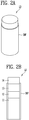
- FIGS. 8 and 9 are views for explaining emission efficiency depending on an alignment relationship between light emitting elements and color conversion elements included in the light emitting device of FIG. 4 .
- FIG. 8 illustrates an angle ANG (or an arrangement angle) of the second alignment direction ADR2 of the color conversion elements QR with respect to the first alignment direction ADR1 of the light emitting elements LD.
- FIG. 9 illustrates the amount of light absorbed in each color conversion element QR (or intensity of light emitted from the color conversion element QR) depending on the angle of the second alignment direction ADR2 of the color conversion element QR.
- the light emitting elements LD included in a light emitting element layer LDL may be aligned in the first alignment direction ADR1
- the color conversion elements QR included in a color conversion layer CCL may be aligned in the second alignment direction ADR2.
- the angle ANG may be an angle of the second alignment direction ADR2 with respect to the first alignment direction ADR1.
- the second alignment direction ADR2 of the color conversion elements QR may form an acute angle of about 30 or less degrees with respect to the first alignment direction ADR1 of the light emitting elements LD, or may be parallel to the first alignment direction ADR1.
- the angle ANG may have a range from about 0 to about 30 degrees.
- the second alignment direction ADR2 may form an acute angle of about 15 or less degrees with respect to the first alignment direction ADR1.
- the second alignment direction ADR2 may be parallel to the first alignment direction ADR1.
- the light absorbed in the color conversion elements QR (or the light emitted from the color conversion elements QR) may be changed to the form of a sine wave depending on the angle ANG between the light emitting elements LD and the color conversion elements QR. Accordingly, as the angle ANG between the light emitting elements LD and the color conversion elements QR becomes closer to about 0, the amount of light absorbed in the color conversion elements QR may be increased, and the intensity of light emitted from the color conversion elements QR may be increased.
- the emission efficiency (or color conversion efficiency) of the color conversion elements QR may be greatly improved.
- the light emitted from the color conversion elements QR may be light polarized in the same direction as the light emitted from the light emitting elements LD. Therefore, the light emitting device EU (see FIG. 4 ) enabling the output of polarized light may maximize the efficiency of a black polarizing film that is additionally attached thereto, and may allow a high-contrast display device to be implemented.
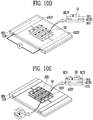
- FIGS. 10a to 10h are views for explaining a process of manufacturing the light emitting device of FIG. 4 .
- first and second common electrodes AELT1 and AELT2 may be formed on a substrate SUB (or in a sub-pixel area SPA of the substrate SUB).
- the area and shape of the substrate SUB are not limited, and may vary in consideration of the area of the first and second common electrodes AELT1 and AELT2 to be formed on the substrate SUB, the size of the light emitting elements LD and the number of light emitting elements LD to be mounted, or the like.
- the thickness of the substrate SUB may be about 100 ⁇ m to about 1 mm.
- the area of the first and second common electrodes AELT1 and AELT2 (or a unit electrode area) may be about 10 ⁇ m 2 to about 100 cm 2 .
- a first insulating layer INS1 may be formed on the second common electrodes AELT1 and AELT2.
- the first insulating layer INS1 may be formed by any one of plasma enhanced chemical vapor deposition (PECVD), e-beam deposition, atomic layer deposition, and sputtering deposition, but the present disclosure is not limited thereto.
- PECVD plasma enhanced chemical vapor deposition
- e-beam deposition atomic layer deposition
- sputtering deposition sputtering deposition
- the first insulating layer INS1 may include at least one material selected from among SiO 2 , Si 3 N 4 , SiN x , Al 2 O 3 , HfO 2 , Y 2 O 3 , and TiO 2 . Also, the first insulating layer INS1 may have a thickness of about 1 nm to about 100 ⁇ m, which may vary in accordance the voltage (e.g., an alignment voltage) of a power supply applied to the first and second common electrodes AELT1 and AELT2, the length of the light emitting elements LD, a distance between the first and second common electrodes AELT1 and AELT2, or the like.
- the voltage e.g., an alignment voltage
- the light emitting elements LD may be provided in a diffused form in a first solution SOL1, and may be provided on the first insulating layer INS1.
- the first solution SOL1 may be manufactured by mixing the light emitting elements LD with a dispersion solvent.
- the dispersion solvent may be the form of ink or paste, and the solvent may be, as a volatile solvent, at least one selected from among acetone, water, alcohol, and toluene.
- the type of dispersion solvent is not limited to the above-described type, and any type of solvent may be used without limitation as long as the solvent may be readily evaporated without exerting physical and chemical influences on the light emitting elements LD.
- the first solution SOL1 may include 0.001 to 100 weight % of the light emitting elements LD, based on the total weight of the dispersion solvent.
- the number of light emitting elements LD coupled to the electrodes may be small.
- the alignment of the light emitting elements LD may be interrupted.
- the light emitting elements LD may be self-aligned between the first and second common electrodes AELT1 and AELT2 in a plan view.
- the solvent may be volatilized or removed using other additional methods, and thus the light emitting elements LD may be stably arranged on the first insulating layer INS1.
- the light emitting elements LD may be arranged with an orientation tendency by an electrostatic attraction between adjacent common electrodes.
- first ends of the light emitting elements LD may be disposed on the first insulating layer INS1 in accordance with the position of the first common electrode AELT1, and second ends thereof having positive charges, may be disposed on the first insulating layer INS1 in accordance with the position of the second common electrode AELT2.
- the first voltage V1 may have a voltage level of about 0.1 V to about 2000 V. In case that the voltage level of the first voltage V1 is less than 0.1 V, the alignment efficiency of the light emitting elements LD may be deteriorated. In case that the voltage level of the first voltage V1 is greater than 2000 V, the first insulating layer INS1 may be broken, and thus a leakage current, an electrical short-circuit, or an electrode damage may occur. Also, the frequency of the first voltage V1 may range from about 10 Hz to about 100 GHz, and the first voltage V1 may be, for example, a sine wave having a frequency of about 90 kHz to about 100 MHz.
- the frequency is less than 10 Hz
- the number of light emitting elements LD that are mounted may be greatly decreased, and the orientation of the light emitting elements LD may be very irregular.
- the frequency is greater than 100 GHz
- the light emitting elements LD may not adapt to rapidly changing AC power, and thus the mountability of the light emitting elements LD may be decreased, and orientation tendency may also be decreased.
- a first electrode ELT1 and a second electrode ELT2 may be respectively formed on the opposite ends of each of the light emitting elements LD.
- the light emitting elements LD may be stably coupled between the first and second electrodes ELT1 and ELT2.
- a process of forming the first and second electrodes ELT1 and ELT2 will be described below with reference to FIGS. 11a to 11e .
- a second insulating layer INS2 may be formed on the light emitting element layer LDL (i.e., the first insulating layer INS1, the light emitting elements LD, and the first and second electrodes ELT1 and ELT2).
- a method of forming the second insulating layer INS2 may be substantially identical or similar to the method of forming the first insulating layer INS1.
- color conversion elements QR may be provided in a diffused form in a second solution SOL2 and may be provided on the second insulating layer INS2.
- a first color conversion element QR1 may be provided on the second insulating layer INS2 in the second sub-pixel area SPA2 (see FIG. 4 )
- a second color conversion element QR2 may be provided on the second insulating layer INS2 in the third sub-pixel area SPA3 (see FIG. 4 ).
- FIGS.10g and 10h illustrate that the color conversion elements QR are sequentially provided and aligned
- the color conversion elements QR may be simultaneously provided and aligned.
- the first color conversion elements QR1 may be simultaneously provided and aligned in a second sub-pixel area SPA2
- the second color conversion elements QR2 may be simultaneously provided and aligned in a third sub-pixel area SPA3.
- FIGS. 11a to 11e are views for explaining a process of forming first and second electrodes of FIG. 10e .
- FIGS. 11a to 11e illustrate as a common electrode layer AEL, a configuration (e.g., a substrate SUB, an additional light emitting element layer, etc.) disposed under the first and second electrodes ELT1 and ELT2.
- a common electrode layer AEL having one surface on which light emitting elements LD are aligned may be provided.
- the common electrode layer AEL may be coated with a photoresist, or in another example, a photoresist layer PR may be formed on the common electrode layer AEL.
- the photoresist layer PR may include a photoresist that is used in the art.
- the common electrode layer AEL may be coated with a photoresist by one of spin coating, spray coating, and screen printing.
- the thickness of the photoresist layer PR may be changed in consideration of the thickness of the first and second electrodes ELT1 and ELT2 to be formed on the common electrode layer AEL, and may be, for example, about 0.1 ⁇ m to about 10 ⁇ m. However, the present disclosure is not limited thereto.
- a mask MASK in which a pattern corresponding to the first and second electrodes ELT1 and ELT2 is printed may be disposed on the photoresist layer PR, and the top of the mask MASK may be exposed to ultraviolet rays (or ultraviolet radiation).
- the photoresist layer PR may be immersed in a typical photoresist solvent, and thus an exposed portion of the photoresist layer PR may be removed.
- the portion of the photoresist layer PR, in which the first and second electrodes ELT1 and ELT2 are to be formed, may be removed.
- an electrode forming material may be deposited on the photoresist layer PR.
- the electrode forming material may be the same as the material forming the first and second electrodes ELT1 and ELT2.
- the photoresist layer PR formed on the common electrode layer AEL may be removed using a photoresist remover.
- the photoresist remover may be any one of acetone, N-methyl pyrrolidone (1-Methyl-2-pyrrolidone (NMP)), and dimethyl sulfoxide (DMSO).
- first and second electrodes ELT1 and ELT2 may be formed on the common electrode layer AEL.
- FIGS. 11a to 11e the first and second electrodes ELT1 and ETL2 are manufactured, the present disclosure is not limited thereto.
- the manufacturing method in FIGS. 11a to 11e may also be applied to first and second common electrodes AELL1 and AELT2. That is, the first and second common electrodes AELL1 and AELT2 and the first and second electrodes ELT1 and ELT2 may be formed using the same manufacturing method.
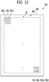
- FIG. 12 is a plan view illustrating a display device according to an embodiment of the present disclosure.
- FIG. 12 illustrates a display device, especially, a display panel PNL provided in the display device, as an example device that may use the light emitting elements LD, described with reference to FIGS. 1a to 3b , or the light emitting device EU, described with reference to FIG. 4 , as a light source.
- FIG. 12 schematically illustrates the structure of the display panel PNL, focusing on a display area DA.
- at least one driving circuit e.g., at least one of a scan driver and a data driver
- a plurality of lines may be further provided on the display panel PNL.
- the display panel PNL may include a first substrate SUB1 and pixels PXL arranged on the first substrate SUB1.
- the display panel PNL and the first substrate SUB1 may include a display area DA in which an image is displayed, and a non-display area NDA other than the display area DA.
- the display area DA may be disposed in a central portion of the display panel PNL, and the non-display area NDA may be disposed along a perimeter portion of the display panel PNL to enclose the display area DA.
- the positions of the display area DA and the non-display area NDA are not limited thereto, and may be changed.
- the first substrate SUB1 may form a base member of the display panel PNL.
- the first substrate SUB1 may form a base member of a lower panel (e.g., a lower plate of the display panel PNL). Since the first substrate SUB1 is substantially identical or similar to the substrate SUB, described above with reference to FIG. 4 , repetitive descriptions thereof will be omitted.
- An area on the first substrate SUB1 may be defined as the display area DA in which the pixels PXL are disposed, and the remaining area thereof may be defined as the non-display area NDA.
- the first substrate SUB may include the display area DA including a plurality of pixel areas in which the pixels PXL are formed, and the non-display area NDA disposed around the display area DA.
- Various lines and/or internal circuits which are coupled to the pixels PXL of the display area DA may be disposed in the non-display area NDA.
- Each pixel PXL may include at least one light emitting element LD driven in response to the corresponding scan signal and the corresponding data signal, for example, at least one rod-type light emitting diode according to any one of the embodiments in FIGS. 1a to 3b .
- the plurality of rod-type light emitting diodes may form a light source of the pixel PXL.
- the pixel PXL may include a plurality of sub-pixels.
- the pixel PXL may include a first sub-pixel SPX1, a second sub-pixel SPX2, and a third sub-pixel SPX3.
- the first, second and third sub-pixels SPX1, SPX2, and SPX3 may emit light of different colors.
- the first sub-pixel SPX1 may be a blue sub-pixel which emits light of a red color
- the second sub-pixel SPX2 may be a green sub-pixel which emits light of a green color
- the third sub-pixel SPX3 may be a blue sub-pixel which emits light of a blue color.
- the colors, types, and/or numbers of sub-pixels forming the pixel PXL are not particularly limited, and in an example, the colors of light emitted from respective sub-pixels may be changed in various manners.
- FIG. 12 illustrates an embodiment in which the pixels PXL are arranged in the form of stripes in the display area DA, the present disclosure is not limited thereto.
- the pixels PXL may be arranged in the form of various pixel arrays.
- the pixels PXL may be formed as active pixels.
- the types, structures, and/or driving schemes of the pixels PXL usable in the display device according to the present disclosure are not limited to particular types, structures, and/or driving schemes.
- each pixel PXL may be formed as a pixel of display devices having various well-known passive or active structures.
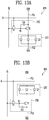
- FIGS. 13a to 13c are circuit diagrams illustrating examples of a sub-pixel included in the display device of FIG. 12 .
- any one of the first, second, and third sub-pixels SPX1, SPX2, and SPX3 illustrated in FIG. 12 is illustrated.
- FIGS. 13a to 13c different embodiments of the sub-pixel SPX that may be provided in an active display device (e.g., an active light emitting display device) are illustrated.
- the sub-pixel SPX illustrated in FIGS. 13a to 13c may be any one of the first, second, and third sub-pixels SPX1, SPX2, and SPX3 provided in the display panel PNL of FIG. 12 , and the first, second, and third sub-pixels SPX1, SPX2, and SPX3 may have a substantially identical or similar structure. Therefore, in FIGS. 13a to 13c , the first, second and third sub-pixels SPX1, SPX2, and SPX3 may be referred to as a sub-pixel SPX.
- the sub-pixel SPX may include an emission unit LSU and a pixel circuit PXC for driving the emission unit LSU.
- the emission unit LSU may include a plurality of light emitting elements LD coupled in parallel to each other between first and second power supplies VDD and VSS.
- the first and second power supplies VDD and VSS may have different potentials.
- the first power supply VDD may be set as a high-potential power supply
- the second power supply VSS may be set as a low-potential power supply.
- a potential difference between the first and second power supplies VDD and VSS may be set to a threshold voltage or more of the light emitting elements LD during at least a light emitting period of the sub-pixel SPX.
- the light emitting elements LD are coupled in parallel to each other in the same direction (e.g., a forward direction) between the first power supply VDD and the second power supply VSS, the present disclosure is not limited thereto.
- some of the light emitting elements LD may be coupled to each other in a forward direction between the first and second power supplies VDD and VSS, and other light emitting elements LD may be coupled to each other in a reverse direction.
- at least one sub-pixel SPX may include only a single light emitting element LD.
- first ends of respective light emitting elements LD may be coupled in common to the corresponding pixel circuit PXC through the first electrode, and may be coupled to the first power supply VDD through the pixel circuit PXC. Second ends of respective light emitting elements LD may be coupled in common to the second power supply VSS through the second electrode.
- the emission unit LSU may emit light with luminance corresponding to a driving current supplied thereto through the corresponding pixel circuit PXC. Thereby, a predetermined image may be displayed in the display area DA.
- the pixel circuit PXC may be coupled to a scan line Si and a data line Dj of the corresponding sub-pixel SPX.
- the pixel circuit PXC of the sub-pixel SPX may be coupled to the i-th scan line Si and the j-th data line Dj of the display area DA.
- the pixel circuit PXC may include first and second transistors T1 and T2, and a storage capacitor Cst.
- the first transistor T1 (or a driving transistor) may be coupled between the first power supply VDD and the first electrode of the emission unit LSU.
- a gate electrode of the first transistor T1 is coupled to a first node N1.
- the first transistor T1 may control the driving current that is supplied to the emission unit LSU in response to the voltage of the first node N1.
- the second transistor T2 (or switching transistor) may be coupled between the data line Dj and the first node N1.
- a gate electrode of the second transistor T2 may be coupled to the scan line Si.
- the second transistor T2 is turned on to connect the data line Dj and the first node N1 to each other.
- a data signal of a corresponding frame may be supplied to the data line Dj, and may be transmitted to the first node N1 via the second transistor T2.
- a voltage corresponding to the data signal may be charged in the storage capacitor Cst.
- a first electrode of the storage capacitor Cst may be coupled to the first power supply VDD, and a second electrode thereof may be coupled to the first node N1.
- the storage capacitor Cst may store a voltage corresponding to the data signal supplied to the first node N1 during each frame period, and may maintain the stored voltage until a data signal of a subsequent frame is supplied thereto.
- the present disclosure is not limited thereto. In other words, at least one of the first and second transistors T1 and T2 may be changed to an N-type transistor.
- both the first and second transistors T1 and T2 may be N-type transistors.
- the sub-pixel SPX illustrated in FIG. 13b may have a configuration and an operation substantially similar to those of the pixel circuit PXC of FIG. 13a , except that the connection positions of some circuit elements are changed depending on a change in a transistor type. Therefore, a description of the sub-pixel SPX of FIG. 13b will be omitted.
- the structure of the pixel circuit PXC is not limited to those in the embodiments illustrated in FIGS. 13a and 13b . That is, the pixel circuit PXC may be formed as pixel circuits having various well-known structures and/or driving schemes. In an example, the pixel circuit PXC may be formed as in the embodiment illustrated in FIG. 13c .
- the pixel circuit PXC may be further coupled to at least one additional scan line (or control line) in addition to a scan line Si for a corresponding horizontal line.
- a pixel circuit PXC of a sub-pixel SPX arranged in an i-th row of a display area DA may be further coupled to an (i-1)-th scan line Si-1 and/or an (i+1)-th scan line Si+1.
- the pixel circuit PXC may be further coupled to other power supplies in addition to the first and second power supplies VDD and VSS.
- the pixel circuit PXC may also be coupled to an initialization power supply Vint.
- the pixel circuit PXC may include first to seventh transistors T1 to T7 and a storage capacitor Cst.
- the first transistor T1 may be coupled between the first power supply VDD and a first electrode of the emission unit LSU.
- a gate electrode of the first transistor T1 may be coupled to a first node N1.
- the first transistor T1 may control a driving current that is supplied to the emission unit LSU in response to the voltage of the first node N1.
- the second transistor T2 may be coupled between a data line Dj and a first electrode of the first transistor T1.
- a gate electrode of the second transistor T2 may be coupled to a corresponding scan line Si.
- the second transistor T2 may be turned on to electrically connect the data line Dj to the first electrode of the first transistor T1. Therefore, in case that the second transistor T2 is turned on, a data signal supplied from the data line Dj may be transmitted to the first transistor T1.
- the third transistor T3 may be coupled between a second electrode of the first transistor T1 and the first node N1.
- a gate electrode of the third transistor T3 may be coupled to the corresponding scan line Si.
- the third transistor T3 may be turned on to electrically connect the first transistor T1 in the form of a diode.
- the fourth transistor T4 may be coupled between the first node N1 and the initialization power supply Vint.
- a gate electrode of the fourth transistor T4 may be coupled to a previous scan line, for example, the (i-1)-th scan line Si-1.
- the fourth transistor T4 may be turned on to transmit the voltage of the initialization power supply Vint to the first node N1.
- the voltage of the initialization power supply Vint may be less than or equal to the lowest voltage of the data signal.
- the fifth transistor T5 may be coupled between the first power supply VDD and the first transistor T1.
- a gate electrode of the fifth transistor T5 may be coupled to a corresponding emission control line, e.g., an i-th emission control line Ei.
- the fifth transistor T5 may be turned off in case that an emission control signal having a gate-off voltage (e.g., a high voltage) is supplied to the emission control line Ei, and may be turned on in other cases.
- a gate-off voltage e.g., a high voltage
- the sixth transistor T6 may be coupled between the first transistor T1 and the first electrode of the emission unit LSU.
- a gate electrode of the sixth transistor T6 may be coupled to the corresponding emission control line, e.g., the i-th emission control line Ei.
- the sixth transistor T6 may be turned off in case that an emission control signal having a gate-off voltage is supplied to the emission control line Ei, and may be turned on in other cases.
- the seventh transistor T7 may be coupled between the first electrode of the emission unit LSU and the initialization power supply Vint.
- a gate electrode of the seventh transistor T7 may be coupled to any one of scan lines in a subsequent stage, e.g., an (i+1)-th scan line Si+1.
- the seventh transistor T7 may be turned on to supply the voltage of the initialization power supply Vint to the first electrode of the emission unit LSU.
- the storage capacitor Cst may be coupled between the first power supply VDD and the first node N1.
- the storage capacitor Cst may store a voltage corresponding to the data signal supplied to the first node N1 and the threshold voltage of the first transistor T1 during each frame period.
- the transistors, e.g., the first to seventh transistors T1 to T7, included in the pixel circuit PXC are P-type transistors
- the present disclosure is not limited thereto.
- at least one of the first to seventh transistors T1 to T7 may be changed to an N-type transistor.
- the voltage level of a control signal e.g., a scan signal and/or a data signal
- the voltage level of a control signal for controlling at least one of the first to seventh transistors T1 to T7 may be changed.
- the structure of the sub-pixel SPX usable in the present disclosure is not limited to those in the embodiments illustrated in FIGS. 13a to 13c , and the sub-pixel SPX may have various well-known structures.
- the pixel circuit PXC included in the sub-pixel SPX may be formed as pixel circuits having various well-known structures and/or driving schemes.
- the sub-pixel SPX may be provided in a passive light emitting display device or the like. In this case, the pixel circuit PXC may be omitted, and each of first and second electrodes of the emission unit LSU may be directly coupled to a scan line Si, a data line Dj, a power line and/or a control line.
- FIGS. 14a and 14b are sectional views illustrating an example of the display device of FIG. 12 .
- the display device may include a first substrate SUB, a pixel circuit layer PCL, a common electrode layer AEL, a light emitting element layer LDL (or a display element layer), and a color conversion layer CCL. Since the first substrate SUB, the common electrode layer AEL, the light emitting element layer LDL, and the color conversion layer CCL are substantially the same as the substrate SUB, the common electrode layer AEL, the light emitting element layer LDL, and the color conversion layer CCL, described above with reference to FIGS. 4 to 6 , repeated descriptions thereof will be omitted.
- the pixel circuit layer PCL may be disposed between the first substrate SUB1 and the light emitting element layer LDL or between the first substrate SUB1 and the common electrode layer AEL.
- the pixel circuit layer PCL may include a pixel circuit PXC, described above with reference to FIGS. 13a to 13c .
- the display device may further include a second substrate SUB2 disposed on the overall surface of the color conversion layer CCL.
- the second substrate SUB2 may be substantially identical or similar to the substrate SUB, described above with reference to FIGS. 4 to 6 .
- the color conversion layer CCL may be manufactured separately from the light emitting element layer LDL, and may be coupled or bonded to the light emitting element layer LDL.
- the color conversion layer CCL may be formed on a first surface of the second substrate SUB2, an upper structure (or an upper panel) including the color conversion layer CCL and the second substrate SUB2 may be coupled to a lower structure (or a lower panel) including the first substrate SUB1 to the light emitting element layer LDL.
- separate common electrodes may be disposed on a second surface of the second substrate SUB2, color conversion elements may be provided, and a voltage may be applied to the common electrodes. Therefore, the color conversion elements may be aligned in a specific direction (e.g., the foregoing second alignment direction), and the common electrodes may be removed from the second substrate SUB2 after the color conversion elements are aligned.
- the upper structure and the lower structure may be aligned with each other such that the second alignment direction of the color conversion elements in the color conversion layer CCL is identical or parallel to the first alignment direction of the light emitting elements LD in the light emitting element layer LDL, and the upper structure may be coupled to the lower structure.
- the color conversion layer CCL may be separately manufactured and coupled to the light emitting element layer LDL without being directly formed on the light emitting element layer LDL, and the second alignment direction of the color conversion elements in the color conversion layer CCL may be substantially identical or parallel to the first alignment direction of the light emitting elements LD in the light emitting element layer LDL.
- the display device (or the display panel PNL) is illustrated as including the alignment electrode layer AEL, the alignment electrode layer AEL may be omitted in some embodiments.
- FIG. 15 is a plan view illustrating an example of a pixel included in the display device of FIG. 12 .
- FIG. 15 illustrates the structure of a pixel PXL, focusing on a light emitting element layer LDL and a color conversion layer CCL of the pixel PXL.
- the pixel PXL may be formed in a pixel area PXA defined on a first substrate SUB.
- the pixel area PXA may include sub-pixel areas SPA corresponding to a plurality of sub-pixels SPX forming the pixel PXL.
- the pixel area PXA may include a first sub-pixel area SPA1 in which a first sub-pixel SPX1 is formed, a second sub-pixel area SPA2 in which a second sub-pixel SPX2 is formed, and a third sub-pixel area SPA3 in which a third sub-pixel SPX3 is formed.
- each of the first to third sub-pixel areas SPA1, SPA2, and SPA3 may include an emission area in which at least one pair of a first electrode ELT1 and a second electrode ELT2 and at least one light emitting element LD coupled between the first and second electrodes ELT1 and ELT2 are arranged.
- the emission area may be defined by a pixel-defining layer enclosing the emission area, partition walls, banks (see FIG. 18 ), or the like.
- first to third sub-pixels SPX1, SPX2, and SPX3 are substantially identical or similar to the sub-pixels SPX1, SPX2, and SPX3 described above with reference to FIGS. 4 to 6 , repeated descriptions thereof will be omitted.
- the first, second and third sub-pixels SPX1, SPX2, and SPX3 may have a substantially identical or similar structure, except for the color conversion elements QR1 and QR2.
- a sub-pixel SPX an area in which the sub-pixel SPX is formed
- a sub-pixel area SPA an area in which the sub-pixel SPX is formed
- the first electrode ELT1 may be coupled to a pixel circuit PXC of the sub-pixel SPX, e.g., the pixel circuit PXC illustrated in any one of FIGS. 13a to 13c , through a first contact hole CH1.
- the first contact hole CH1 may be disposed outside the emission area of each sub-pixel SPX.
- the pixel circuit PXC may be disposed under the light emitting elements LD arranged in a corresponding sub-pixel area SPA.
- each pixel circuit PXC may be formed in a pixel circuit layer (or a circuit element layer including circuit elements, such as transistors) under the light emitting elements LD, and may be coupled to the first electrode ELT1 through the first contact hole CH1.
- the second electrode ELT2 may be coupled to a second power supply VSS (see FIG. 13a ).
- the second electrode ELT2 may be coupled to the second power supply VSS through a second contact hole CH2 and a power line (not illustrated) coupled thereto.
- the second contact hole CH2 may be disposed outside the emission area of each sub-pixel SPX, but the present disclosure is not limited thereto.
- an area of a power line for supplying the second power supply VSS may be disposed in a pixel circuit layer under the light emitting elements LD.
- the power line may be disposed in the pixel circuit layer PCL (see FIG. 14a ) under the light emitting elements LD, and may be coupled to the second electrode ELT2 through the second contact hole CH2.
- the present disclosure is not limited thereto, and the position of the power line may be changed in various manners.
- all of the light emitting elements LD may be blue light emitting diodes which emit light of a blue color.
- a first color conversion element QR1 e.g., a green quantum rod for converting blue light into green light
- a second color conversion element QR2 e.g., a red quantum rod for converting blue light into red light
- each of the first and second color conversion elements QR1 and QR2 may have a rod-like shape, and may be disposed between first and second electrodes ELT1 and ELT2 of the corresponding sub-pixel area SPX, and in an example, most of first and second color conversion elements QR1 and QR2 may be disposed between the first and second electrodes ELT1 and ELT2 of the corresponding sub-pixel area SPX.
- the second alignment direction ADR2 of the first and second color conversion elements QR1 and QR2 may be identical to or substantially the same as the first alignment direction ADR1 of the light emitting elements LD arranged in the corresponding sub-pixel area SPX.
- FIG. 16a is a sectional view illustrating an example of the pixel taken along line II-II' of FIG. 15 .
- FIG. 16a an example of the pixel included in the display device of FIG. 14a is illustrated.
- a pixel circuit layer PCL, a common electrode layer AEL, a light emitting element layer LDL, and a color conversion layer CCL may be sequentially arranged in a pixel area SPA on a first substrate SUB1.
- the common electrode layer AEL, the pixel circuit layer PCL, and the light emitting element layer LDL may be formed on the entire display area DA of the display panel PNL.
- the pixel circuit layer PCL may include circuit elements forming the pixel circuit PXC of the pixel PXL.
- the pixel circuit layer PCL may include a plurality of transistors, e.g., first transistors T1 of FIGS. 13a and 13b , arranged in the pixel area PXA.
- the pixel circuit layer PCL may include a storage capacitor Cst arranged in the pixel area PXL, various types of signal lines (e.g., a scan line Si and a data line Dj of FIGS.
- the pixel circuit layer may have a sectional structure substantially identical or similar to that of the plurality of transistors provided in the pixel circuit PXC, for example, the first transistor T1.
- the present disclosure is not limited thereto, and in other embodiments, at least some of the plurality of transistors may have different types and/or structures.
- the pixel circuit layer PCL may include a plurality of insulating layers.
- the pixel circuit layer PCL may include a buffer layer BFL, a gate insulating layer GI, an interlayer insulating layer ILD, and a passivation layer PSV which are sequentially stacked each other on a surface of the substrate SUB.
- the buffer layer BFL may prevent impurities from being diffused to circuit elements.
- the buffer layer BFL may be formed in a single layer structure, but may be formed in a multi-layer structure having two or more layers. In case that the buffer layer BFL is formed in a multi-layer structure, the respective layers may be formed of the same material or different materials. Meanwhile, in embodiments, the buffer layer BFL may be omitted.
- the first transistor T1 may include a semiconductor layer SCL, a gate electrode GE, a first transistor electrode ET1, and a second transistor electrode ET2.
- FIG. 16a illustrates the first transistor T1 has the first transistor electrode ET1 and the second transistor electrode ET2 formed separately from the semiconductor layer SCL, the present disclosure is not limited thereto.
- first and/or second transistor electrodes ET1 and ET2 provided in at least one transistor arranged in the pixel area PXL may be integral with respective semiconductor layers SCL.
- the semiconductor layer SCL may be disposed on the buffer layer BFL.
- the semiconductor layer SCL may be disposed between the substrate SUB on which the buffer layer BFL is formed and the gate insulating layer GI.
- the semiconductor layer SCL may include a first region contacting the first transistor electrode ET1, a second region contacting the second transistor electrode ET2, and a channel region disposed between the first and second regions.
- one of the first and second regions may be a source region and the other thereof may be a drain region.
- the semiconductor layer SCL may be a semiconductor pattern formed of polysilicon, amorphous silicon, an oxide semiconductor, or the like.
- the channel region of the semiconductor layer SCL may be an intrinsic semiconductor as a semiconductor pattern undoped with impurities, and the first and second regions of the semiconductor layer SCL may be semiconductor patterns doped with predetermined impurities.
- the gate electrode GE may be disposed on the semiconductor layer SCL with the gate insulating layer GI interposed therebetween.
- the gate electrode GE may be disposed between the gate insulating layer GI and the interlayer insulating layer ILD so as to overlap at least a portion of the semiconductor layer SCL.
- the first and second transistor electrodes ET1 and ET2 may be disposed on the semiconductor layer SCL and the gate electrode GE with at least one interlayer insulating layer IDL interposed therebetween.
- the first and second transistor electrodes ET1 and ET2 may be interposed between the interlayer insulating layer ILD and the passivation layer PSV.
- the first and second transistor electrodes ET1 and ET2 may be electrically coupled to the semiconductor layer SCL.
- the first and second transistor electrodes ET1 and ET2 may be respectively coupled to the first region and the second region of the semiconductor layer SCL through contact holes passing through the gate insulating layer GI and the interlayer insulating layer ILD.
- any one of the first and second transistor electrodes ET1 and ET2 of at least one transistor may be electrically coupled to a bridge electrode ELT_BRP disposed on the top of the passivation layer PSV through the first contact hole CH1 passing through the passivation layer PSV.
- At least one signal line and/or power line coupled to the pixel PXL may be disposed on the same layer as first electrodes of the circuit elements forming the pixel circuit PXC.
- a power line PL e.g., a second power line for supplying the second power supply VSS
- a power line PL may be disposed on the same layer as the gate electrode GE of the first transistor T1, and may be coupled to the second common electrode AELT2 disposed on the top of the passivation layer PSV, through a bridge pattern BRP that is disposed on the same layer as the first and second transistor electrodes ET1 and ET2 and through at least one second contact hole CH2 that passes through the passivation layer PSV.
- the structure and/or position of the power line PL may be changed in various manners.
- the common electrode layer AEL may include the first common electrode AELT1 and the second common electrode AELT2. Since the first and second common electrodes AELT1 and AELT2 are substantially identical to the first and second common electrodes AELT1 and AELT2 described above with reference to FIGS. 4 to 6 , repeated descriptions thereof will be omitted.
- the common electrode layer AEL may further include the bridge electrode ELT_BRP.
- the bridge electrode ELT_BRP may couple the first electrode ELT1 of the light emitting element layer LDL to the first transistor T1 (or the first transistor electrode ET1) of the pixel circuit layer PCL.
- the light emitting element layer LDL is substantially the same as the light emitting element layer LDL, described above with reference to FIG. 6 , repeated descriptions thereof will be omitted.
- the second electrode ELT2 of the light emitting element layer LDL may be coupled to the second common electrode AELT2 via a through hole passing through the first insulating layer INS1.
- the first electrode ELT1 of the light emitting element layer LDL may be coupled to the first transistor T1 (or the first transistor electrode ET1) of the pixel circuit layer PCL via the through hole passing through the insulating layers INS1 and the bridge electrode ELT_BRP.
- color conversion layer CCL is substantially the same as the color conversion layer CCL, described above with reference to FIG. 6 , repeated descriptions thereof will be omitted.
- the second common electrode AELT2 is illustrated as being coupled to the second electrode ELT2 of the light emitting element layer LDL, the present disclosure is not limited thereto.
- the second electrode ELT2 of the light emitting element layer LDL may be coupled to the power line PL through a separate bridge electrode without being coupled to the second common electrode AELT2.
- FIG. 16b is a sectional view illustrating another example of the pixel taken along line II-II' of FIG. 15 .
- FIG. 16b an example of the pixel included in the display device of FIG. 14b is illustrated.
- the pixel of FIG. 16b may be substantially identical or similar to that of FIG. 16a in that the former includes a color conversion layer CCL and a second substrate SUB2. Therefore, repeated descriptions thereof will be omitted.
- the color conversion layer CCL may include a color conversion element QR and an overcoat layer OC (or an insulating layer).
- the color conversion element QR may be formed on a first surface (e.g., a bottom surface in FIG. 14b ) of the second substrate SUB2.
- the overcoat layer OC may be disposed on the entirety of the first surface of the second substrate SUB2, and may cover the color conversion element QR.
- the overcoat layer OC may be substantially identical or similar to the first and second insulating layers INS1 and INS2, described above with reference to FIGS. 4 to 6 .
- An upper structure (or an upper panel) including the color conversion layer CCL and the second substrate SUB2 may be coupled to a lower structure (or a lower panel) including the first substrate SUB1 to the light emitting element layer LDL. Therefore, the overcoat layer OC may be disposed on the second insulating layer INS2, the second substrate SUB2 may be disposed on the overcoat layer OC, and the color conversion element QR may be disposed between the overcoat layer OC (or the second insulating layer INS2) and the second substrate SUB2.
- a second alignment direction of the color conversion element QR in the color conversion layer CCL may be substantially identical or parallel to a first alignment direction of the light emitting elements LD in the light emitting element layer LDL.
- the color conversion element QR is illustrated as overlapping the light emitting element LD in a third direction DR3, this is merely exemplary and the present disclosure is not limited thereto.
- the color conversion element QR since the color conversion element QR is formed independently of the second substrate SUB2, the color conversion element QR may not overlap the light emitting element LD, and the color conversion element QR may not be disposed between the first and second electrodes ELT1 and ELT2 (or the first and second common electrodes AELT1 and AELT2) in a plan view.
- FIGS. 17a to 17d are sectional views illustrating a further example of the pixel taken along line II-II' of FIG. 15 .
- the pixels in FIGS. 17a to 17d may be substantially identical or similar to the pixel of FIG. 16b except for the light emitting element layer LDL, and thus repeated descriptions thereof will be omitted.
- the light emitting element layer LDL may include first and second partition walls PW1 and PW2, first and second electrodes ELT1 and ELT2, a first insulating layer INS1, light emitting elements LD, a second insulating layer INS2, first and second contact electrodes CNE1 and CNE2, and a third insulating layer INS3 which are sequentially disposed and/or formed on a pixel circuit layer PCL.
- the first and second partition walls PW1 and PW2 may be disposed on the pixel circuit layer PCL.
- the first and second partition walls PW1 and PW2 may be arranged in an emission area to be spaced apart from each other.
- the first and second partition walls PW1 and PW2 may protrude from the pixel circuit layer PCL in a height direction.
- the first and second partition walls PW1 and PW2 may have, but are not limited to, substantially the same height.
- the first partition wall PW1 may be disposed between the pixel circuit layer PCL and the first electrode ELT1.
- the first partition wall PW1 may be arranged adjacent to first ends EP1 of the light emitting elements LD.
- a side surface of the first partition wall PW1 may be positioned adjacent to the first ends EP1 of the light emitting elements LD, and may face the first ends EP1.
- the second partition wall PW2 may be disposed between the pixel circuit layer PCL and the second electrode ELT2.
- the second partition wall PW2 may be arranged adjacent to second ends EP2 of the light emitting elements LD.
- a side surface of the second partition wall PW2 may be positioned adjacent to the second ends EP2 of the light emitting elements LD, and may then face the second ends EP2.
- first and second partition walls PW1 and PW2 may have various shapes.
- each of the first and second partition walls PW1 and PW2 may have a cross-sectional shape of a trapezoid, the width of which decreases toward the top thereof, as illustrated in FIG. 17a .
- each of the first and second partition walls PW1 and PW2 may have a sloped surface on at least one side surface thereof.
- each of the first and second partition walls PW1 and PW2 may have a cross-sectional shape of a semicircle or a semiellipse, the width of which decreases toward the top thereof.
- each of the first and second partition walls PW1 and PW2 may have a curved surface as at least one side surface thereof.
- first and second partition walls PW1 and PW2 are not limited to particular shapes, and may be changed in various manners. Also, in an embodiment, at least one of the first and second partition walls PW1 and PW2 may be omitted, or, the position thereof may be changed.
- the first and second partition walls PW1 and PW2 may include an insulating material including an inorganic material and/or an organic material.
- the first and second partition walls PW1 and PW2 may include at least one inorganic layer which contains various well-known inorganic insulating materials (including SiN x or SiO x ).
- the first and second partition walls PW1 and PW2 may include at least one organic layer including various well-known organic insulating materials and/or a photoresist layer, or may be formed of a single layer or a multi-layer insulator including organic/inorganic materials in combination. That is, materials forming the first and second partition walls PW1 and PW2 may be changed in various manners.
- first and second partition walls PW1 and PW2 may function as reflective members.
- first and second partition walls PW1 and PW2 along with the first and second electrodes ELT1 and ELT2 provided on the top thereof, may function as reflective members for improving optical efficiency of the pixel PXL by inducing light emitted from respective light emitting elements LD in a desired direction.
- the first and second electrodes ELT1 and ELT2 may be respectively disposed on the tops of the first and second partition walls PW1 and PW2.
- the first and second electrodes ELT1 and ELT2 may be spaced apart from each other.
- the first and second electrodes ELT1 and ELT2 respectively disposed on the tops of the first and second partition walls PW1 and PW2 may have shapes corresponding to those of the first and second partition walls PW1 and PW2, respectively.
- the first and second electrodes ELT1 and ELT2 have sloped surfaces or curved surfaces corresponding to the first and second partition walls PW1 and PW2, they may protrude in the height direction (or the thickness direction) of the pixel circuit layer PCL.
- Each of the first and second electrodes ELT1 and ELT2 may include at least one conductive material.
- each of the first and second electrodes ELT1 and ELT2 may include, but is not limited to, a material corresponding to at least one of a metal such as Ag, Mg, Al, Pt, Pd, Au, Ni, Nd, Ir, Cr, Ti, and an alloy thereof, a conductive oxide such as ITO, IZO, ZnO, or ITZO, and a conductive polymer such as PEDOT.
- each of the first and second electrodes ELT1 and ELT2 may be formed in a single layer structure or a multi-layer structure.
- each of the first and second electrodes ELT1 and ELT2 may include at least one reflective electrode layer.
- each of the first and second electrodes ELT1 and ELT2 may selectively further include at least one of at least one transparent electrode layer disposed on and/or under the reflective electrode layer and at least one conductive capping layer configured to cover the top of the reflective electrode layer and/or the transparent electrode layer.
- the reflective electrode layer of each of the first and second electrodes ELT1 and ELT2 may be made of a conductive material having uniform reflectivity.
- the reflective electrode layer may include, but is not limited to, at least one of metals such as Ag, Mg, Al, Pt, Pd, Au, Ni, Nd, Ir, Cr, and an alloy thereof. That is, the reflective electrode layer may be made of various types of reflective conductive materials.
- each of the first and second electrodes ELT1 and ELT2 includes a reflective electrode layer
- light emitted from the opposite ends of each of the light emitting elements LD that is, the first and second ends EP1 and EP2
- first and second electrodes ELT1 and ELT2 face the first and second ends EP1 and EP2 of the light emitting elements LD while having a sloped surface or a curved surface corresponding to the shapes of the first and second partition walls PW1 and PW2
- light emitted from the first and second ends EP1 and EP2 of each of the light emitting elements LD may be reflected from the first and second electrodes ELT1 and ELT2 to further travel in the frontal direction of the display panel PNL (e.g., from the upward direction of the base layer SUB1). Accordingly, the efficiency of light emitted from the light emitting elements LD may be improved.
- each of the first and second electrodes ELT1 and ELT2 may be made of various types of transparent electrode materials.
- the transparent electrode layer may include, but is not limited to, ITO, IZO or ITZO.
- each of the first and second electrodes ELT1 and ELT2 may be formed in a triple-layer structure having a stacked structure of ITO/Ag/ITO.
- a voltage drop attributable to a signal delay (RC delay) may be minimized. Accordingly, a desired voltage may be effectively transferred to the light emitting elements LD.
- each of the first and second electrodes ELT1 and ELT2 includes the conductive capping layer for covering a reflective electrode layer and/or a transparent electrode layer
- the reflective electrode layers of the first and second electrodes ELT1 and ELT2 may be prevented from being damaged by defects occurring in a process for manufacturing pixels PXL.
- the conductive capping layer may be selectively included in the first and second electrodes ELT1 and ELT2, and may be omitted in some embodiments.
- the conductive capping layer may be regarded as the component of each of the first and second electrodes ELT1 and ELT2, or as a separate component disposed on the first and second electrodes ELT1 and ELT2.
- the first insulating layer INS1 may be disposed on portions of the first and second electrodes ELT1 and ELT2.
- the first insulating layer INS1 may cover portions of the first and second electrodes ELT1 and ELT2, and may include an opening that exposes other portions of the first and second electrodes ELT1 and ELT2.
- the first insulating layer INS1 may primarily cover the overall surfaces of the first and second electrodes ELT1 and ELT2. After the light emitting elements LD have been provided and aligned on the first insulating layer INS1, the first insulating layer INS1 may be partially opened to expose the first and second electrodes ELT1 and ELT2. Alternatively, after the provision and alignment of the light emitting elements LD have been completed, the first insulating layer INS1 may be patterned in the form of an individual pattern that are locally disposed under the light emitting elements LD.
- the first insulating layer INS1 may be interposed between the first and second electrodes ELT1 and ELT2 and the light emitting elements LD, and may expose at least a portion of each of the first and second electrodes ELT1 and ELT2.
- the first insulating layer INS1 may cover the first and second electrodes ELT1 and ELT2 after the first and second electrodes ELT1 and ELT2 have been formed, thereby preventing the first and second electrodes ELT1 and ELT2 from being damaged or metal from being extracted during a subsequent process. Further, the first insulating layer INS1 may stably hold each light emitting element LD.
- the light emitting elements LD may be provided and aligned on the first insulating layer INS1.
- the light emitting elements LD may be provided by an inkjet method or the like, and the light emitting elements LD may be aligned between the first and second electrodes ELT1 and ELT2 by a predetermined voltage (e.g., an alignment signal) applied to the first and second electrodes ELT1 and ELT2.
- a predetermined voltage e.g., an alignment signal
- the second insulating layer INS2 may be disposed on the top of the light emitting elements LD, especially the light emitting elements LD aligned between first and second electrodes ELT1 and ELT2, and may expose the first and second ends EP1 and EP2 of the light emitting elements LD.
- the second insulting layer INS2 may be partially disposed only on the tops of portions of the light emitting elements LD without covering the first and second ends EP1 and EP2 of the light emitting elements LD.
- the second insulating layer INS2 may be formed as, but is not limited to, an independent pattern in each of the sub-pixel areas. Further, as illustrated in FIG.
- the space may be filled with the second insulating layer INS2. Accordingly, the light emitting elements LD may be more stably held.
- the first and second contact electrodes CNE1 and CNE2 may be disposed on the first and second electrodes ELT1 and ELT2 and the first and second ends EP1 and EP2 of the light emitting elements LD. In an embodiment, the first and second contact electrodes CNE1 and CNE2 may be disposed on the same layer, as illustrated in FIG. 17a .
- the first and second contact electrodes CNE1 and CNE2 may be formed by the same process using the same conductive material, but the present disclosure is not limited thereto.
- the first and second contact electrodes CNE1 and CNE2 may electrically couple the first and second ends EP1 and EP2 of the light emitting elements LD to the first and second electrodes ELT1 and ELT2, respectively.
- the first contact electrode CNE1 may be disposed on the first electrode ELT1 so as to contact the first electrode ELT1.
- the first contact electrode CNE1 may contact the first electrode ELT1 in a portion of the first electrode ELT1 (e.g., the first contactor), which is not covered with the first insulating layer INS1.
- the first contact electrode CNE1 may be disposed on the first ends EP1 of the plurality of light emitting elements LD so as to contact the first end EP1 of at least one light emitting element LD adjacent to the first electrode ELT1, e.g., the first ends EP1 of the plurality of light emitting elements LD.
- the first contact electrode CNE1 may be disposed to cover the first ends EP1 of the light emitting elements LD and at least one portion of the first electrode ELT1 corresponding thereto.
- the first ends EP1 of the light emitting elements LD may be electrically coupled to the first electrode ELT1.
- the second contact electrode CNE2 may be disposed on the second electrode ELT2 so as to contact the second electrode ELT2.
- the second contact electrode CNE2 may contact the second electrode ELT2 in a portion of the second electrode ELT2 (e.g., the second contactor), which is not covered with the first insulating layer INS1.
- the second contact electrode CNE2 may be disposed on the second ends EP2 to contact the second end EP2 of at least one light emitting element LD adjacent to the second electrode ELT2, e.g., the second ends EP2 of the plurality of light emitting elements LD.
- the second contact electrode CNE2 may cover the second ends EP2 of the light emitting elements LD and at least one portion of the second electrode ELT2 corresponding thereto.
- the second ends EP2 of the light emitting elements LD may be electrically coupled to the second electrode ELT2.
- the third insulating layer INS3 may be formed and/or disposed on a first surface of the first substrate SUB1 on which the first and second partition walls PW1 and PW2, the first and second electrodes ELT1 and ELT2, the light emitting elements LD, and the first and second contact electrodes CNE1 and CNE2 are formed such that the third insulating layer INS3 covers the first and second partition walls PW1 and PW2, the first and second electrodes ELT1 and ELT2, the light emitting elements LD, and the first and second contact electrodes CNE1 and CNE2.
- the third insulating layer INS3 may include, but is not limited to, a thin film encapsulation layer including at least one inorganic layer and/or at least one organic layer. Further, in an embodiment, at least one overcoat layer, not illustrated, may be further disposed on the top of the third insulating layer INS3.
- each of the first to third insulating layers INS1, INS2, and INS3 may be configured in a single layer or multi-layer structure, and may include at least one inorganic insulating material and/or at least one organic insulating material.
- each of the first to third insulating layers INS1, INS2, and INS3 may include various well-known organic/inorganic insulating materials including SiN x , and the material forming each of the first to third insulating layers INS1, INS2, and INS3 is not particularly limited.
- first to third insulating layers INS1, INS2, and INS3 may include different types of insulating materials, or alternatively, at least some of the first to third insulating layers INS1, INS2, and INS3 may include the same insulating material.
- the color conversion layer CCL including the color conversion elements QR may be formed on a first surface (e.g., a bottom surface in FIG. 14b ) of the second substrate SUB2, and an upper structure (or an upper panel) including the color conversion layer CCL and the second substrate SUB2 may be disposed on a lower structure (or a lower panel) including the first substrate SUB1 to the light emitting element layer LDL.
- the color conversion layer CCL may be spaced apart from the light emitting element layer LDL, but the present disclosure is not limited thereto.
- first and second contact electrodes CNE1 and CNE2 may be disposed on different layers.
- the first contact electrode CNE1 may be arranged in a sub-pixel area SPA in which the second insulating layer INS2 is disposed.
- the first contact electrode CNE1 may be disposed on the first electrode ELT1 to contact a portion of the first electrode ELT1 arranged in the corresponding sub-pixel area SPA.
- the first contact electrode CNE1 may be disposed on the first end EP1 of at least one light emitting element LD arranged in the corresponding sub-pixel area SPA so as to contact the first end EP1.
- the first end EP1 of at least one light emitting element LD arranged in the sub-pixel area SPA may be electrically coupled to the first electrode ELT1 arranged in the corresponding sub-pixel area SPA.
- a fourth insulating layer INS4 may be arranged in the sub-pixel area SPA in which the first contact electrode CNE1 is arranged.
- the fourth insulating layer INS4 may cover the second insulating layer INS2 and the first contact electrode CNE1 which are arranged in the corresponding sub-pixel area SPA.
- the fourth insulating layer INS4 may be formed in a single layer or multi-layer structure, and may include at least one inorganic insulating material and/or at least one organic insulating material.
- the fourth insulating layer INS4 may include various well-known organic/inorganic insulating materials including SiN x .
- the fourth insulating layer INS4 may include an insulating material different from those of the first to third insulating layers INS1, INS2, and INS3, or may include an insulating material identical to those of at least some of the first to third insulating layers INS1, INS2, and INS3.
- a second contact electrode CNE2 may be arranged in each sub-pixel area SPA in which the fourth insulating layer INS4 is arranged.
- the second contact electrode CNE2 may be disposed on the second electrode ELT2 to contact a portion of the second electrode ELT2 arranged in the corresponding sub-pixel area SPA.
- the second contact electrode CNE2 may be disposed on the second end EP2 of at least one light emitting element LD arranged in the corresponding sub-pixel area SPA so as to contact the second end EP2.
- the second end EP2 of at least one light emitting element LD arranged in each sub-pixel area SPA may be electrically coupled to the second electrode ELT2 arranged in the corresponding sub-pixel area SPA.
- the third insulating layer INS3 may be formed and/or disposed on a first surface of the first substrate SUB1 on which the first and second partition walls PW1 and PW2, the first and second electrodes ELT1 and ELT2, the light emitting elements LD, and the first and second contact electrodes CNE1 and CNE2 are formed such that the third insulating layer INS3 covers the first and second partition walls PW1 and PW2, the first and second electrodes ELT1 and ELT2, the light emitting elements LD, and the first and second contact electrodes CNE1 and CNE2.
- the pixel (or sub-pixel) of FIG. 17d is different from the pixel of FIG. 17c in that the pixel of FIG. 17d includes first and second partition walls PW1 and PW2 having a cross-sectional shape of a semicircle or a semiellipse.
- each of the first and second partition walls PW1 and PW2 may have a cross-sectional shape of a semicircle or a semiellipse, the width of which decreases toward the top thereof.
- each of the first and second partition walls PW1 and PW2 may have a curved surface on at least one side surface thereof.
- FIG. 18 is a sectional view illustrating an example of the display device taken along line III-III' of FIG. 15 .
- a pixel circuit layer PCL is omitted, and the structure of a pixel PXL is schematically illustrated based on a light emitting element layer LDL and a color conversion layer CCL.
- the pixel PXL of FIG. 18 may be different from those illustrated in FIGS. 17a to 17d in that former further includes banks BNK.
- the banks BNK may be disposed on a first substrate SUB1 (or the pixel circuit layer PCL illustrated in FIGS. 17a to 17d ). In embodiments, the banks BNK may be directly disposed on the first insulating layer INS1 illustrated in FIGS. 17a to 17d .
- the banks BNK may be formed between the sub-pixels SPX to enclose an emission area EMA of each of the sub-pixels SPX, and may form a pixel defining layer for partitioning the emission area EMA of the sub-pixel SPX. That is, the emission area EMA of the first sub-pixel SPX1, the emission area EMA of the second sub-pixel SPX2, and the emission area EMA of the third sub-pixel SPX3 may be defined by the banks BNK.
- Each bank BNK may block light emitted from the light emitting elements LD of each sub-pixel SPX from passing through the bank BNK, thereby preventing optical interference from occurring in case that the light emitted from each emission area EMA enters an adjacent emission area EMA.
- the banks BNK may protrude from the first substrate SUB1 in a height direction.
- the height of the banks BNK may be greater than that of the light emitting element layer (i.e., the light emitting element layer except for the bank BNK), and may be, for example, equal to or greater than about 2 ⁇ m, or equal to or greater than about 2.5 ⁇ m.
- the banks BNK may function as a dam structure for preventing a solution mixed with the light emitting elements LD from flowing into the emission area EMA of an adjacent pixel PX, or for controlling a predetermined amount of solution to be supplied to each emission area EMA.
- the color conversion layer CCL may include color conversion elements QR1 and QR2, color filters CF1, CF2, and CF3, and a black matrix BM.
- the first color filter CF1 may be disposed on a first surface (e.g., a bottom surface in FIG. 18 ) of the second substrate SUB2, may overlap the first sub-pixel area SPA1 (or the emission area EMA of the first sub-pixel area SPA1), and may selectively transmit light of a first color, emitted from the light emitting elements LD.
- the first color filter CF1 may be a first color transmission filter (e.g., a blue transmission filter) which transmits only a first color (e.g., blue).
- the second color filter CF2 may be disposed on the first surface (e.g., the bottom surface in FIG. 18 ) of the second substrate SUB2, may overlap the second sub-pixel area SPA2 (or the emission area EMA of the second sub-pixel area SPA2), and may selectively transmit light of a second color, emitted through the first color conversion element QR1.
- the second color filter CF2 may be a second color transmission filter (e.g., a green transmission filter) which transmits only a second color (e.g., green).
- the third color filter CF3 may be disposed on the first surface (e.g., the bottom surface in FIG. 18 ) of the second substrate SUB2, may overlap the third sub-pixel area SPA3 (or the emission area EMA of the third sub-pixel area SPA3), and may selectively transmit light of a third color, emitted through the second color conversion element QR2.
- the third color filter CF3 may be a third color transmission filter (e.g., a red transmission filter) which transmits only a third color (e.g., red).
- all of the light emitting elements LD may emit light of the same color.
- a color conversion layer CCL may be disposed on the top of at least some of the first, second, and third sub-pixels SPX1, SPX2, and SPX3. Therefore, the display device according to an embodiment of the present disclosure may display a full-color image.
- Black matrices BM may be disposed between the first, second, and third color filters CF1, CF2, and CF3.
- black matrices BM may be disposed on the first surface (e.g., a bottom surface in FIG. 18 ) of the second substrate SUB2 so as to overlap the banks BNK on the first substrate SUB1.
- color conversion elements QR1 and QR2 and color filters CF may be disposed on at least some sub-pixels SPX, and thus a full-color pixel PXL and a display device having the full-color pixel PXL may be implemented.
- respective sub-pixels SPX may form respective light emitting devices.
- a first sub-pixel SPX1 corresponding to a red sub-pixel may form a blue light emitting device
- a second sub-pixel SPX2 corresponding to a green sub-pixel may form a green light emitting device
- a third sub-pixel SPX3 corresponding to a blue sub-pixel may form a red light emitting device.
- a full-color pixel PXL including the first, second, and third sub-pixels SPX1, SPX2, and SPX3 may form a full-color light emitting device. That is, the embodiment of the present disclosure is not necessarily limited to a display device, and may also be widely applied to other types of devices requiring light sources.
Landscapes
- Electroluminescent Light Sources (AREA)
Abstract
Description
- Various embodiments of the present disclosure relate to a light emitting device, a display device having the light emitting device, and a method of manufacturing the display device.
- Recently, a technique of manufacturing a subminiature light emitting element using a material having a highly reliable inorganic crystal structure and manufacturing a light emitting device using the light emitting element has been developed. For example, technology for configuring a light source of a light emitting device using subminiature light emitting elements having a small size ranging from a nanoscale to a microscale has been developed. Such a light emitting device may be used in various electronic devices such as a display device or a lighting device.
- A full color light emitting device may be implemented using monochromatic (e.g., blue) light emitting elements and color conversion elements (i.e., a color conversion material for converting the color of incident light to another color and then emitting the converted light).
- However, rod-type light emitting elements emit linearly polarized light, and quantum dots generally used as the color conversion elements absorb the linearly polarized light and emit light in a Lambertian form, thus deteriorating emission efficiency of light finally emitted from the light emitting device.
- The technical object of the present disclosure is to provide a light emitting device having improved emission efficiency and a display device having the light emitting device.
- The technical object of the present disclosure is to provide a display device manufacturing method of manufacturing the display device.
- In order to accomplish an object of the present disclosure, a light emitting device according to embodiments of the present disclosure may include a substrate; a light emitting element layer disposed on the substrate and including light emitting elements having a rod shape; and a color conversion layer disposed on the light emitting element layer and including color conversion elements having a rod shape, wherein a second alignment direction of the color conversion elements is substantially identical to a first alignment direction of the light emitting elements.
- According to an embodiment, each of the color conversion elements may be a quantum rod.
- According to an embodiment, the quantum rod may convert first monochromatic light emitted from the light emitting elements into second monochromatic light.
- According to an embodiment, an angle formed between the second alignment direction and the first alignment direction may be 30 or less degrees.
- According to an embodiment, the first alignment direction may be a direction in which 3/4 or more of the light emitting elements are arranged, and the second alignment direction may be a direction in which 3/4 or more of the color conversion elements are arranged.
- According to an embodiment, the light emitting element layer may further include a first electrode and a second electrode disposed on the substrate and spaced apart from each other; and a first insulating layer disposed on the first and second electrodes and the substrate, wherein the light emitting elements are disposed between the substrate and the first insulating layer and between the first electrode and the second electrode.
- According to an embodiment, the light emitting device may further include a common electrode layer disposed between the substrate and the light emitting element layer; and a second insulating layer disposed between the common electrode layer and the light emitting element layer, wherein the common electrode layer includes a first common electrode and a second common electrode disposed to be spaced apart from each other, wherein the first common electrode overlaps the first electrode and may be electrically disconnected from the first electrode, and wherein the second common electrode overlaps the first common electrode.
- According to an embodiment, the light emitting elements may be disposed between the first and second electrodes and the second insulating layer, respective first ends of the light emitting elements may be coupled to the first electrode, and respective second ends of the light emitting elements may be coupled to the second electrode.
- According to an embodiment, the color conversion elements may be disposed between the first common electrode and the second common electrode in a plan view.
- According to an embodiment, the substrate may include a first sub-pixel area, a second sub-pixel area, and a third sub-pixel area, the light emitting elements may emit light of a first color, the color conversion elements may include a first color conversion element arranged in the second sub-pixel area and configured to convert the light of the first color into light of a second color, and a second color conversion element arranged in the third sub-pixel area and configured to convert the light of the first color into light of a third color.
- In order to accomplish an object of the present disclosure, a display device according to embodiments of the present disclosure may include a first substrate; a light emitting element layer including light emitting elements and disposed on the first substrate; a color conversion layer including color conversion elements having a rod shape and disposed on the light emitting element layer; and a second substrate disposed on the color conversion layer, wherein a second alignment direction of the color conversion elements may be parallel to a first alignment direction of the light emitting elements.
- According to an embodiment, the light emitting element layer may further include a first electrode and a second electrode disposed on the first substrate and spaced apart from each other, and the light emitting elements are disposed between the first electrode and the second electrode.
- According to an embodiment, the display device may further include a pixel circuit layer disposed between the first substrate and the light emitting element layer and including transistors and a power line, wherein the first electrode may be coupled to a first electrode of a first transistor, among the transistors, through a first contact hole passing through at least a part of the pixel circuit layer, and the second electrode may be coupled to the power line through a second contact hole passing through at least a part of the pixel circuit layer.
- According to an embodiment, the light emitting element layer may further include a first contact electrode configured to couple a first end of each of the light emitting elements to the first electrode; and a second contact electrode configured to couple a second end of each of the light emitting elements to the second electrode, and the first contact electrode and the second contact electrode are disposed on an identical layer.
- According to an embodiment, the light emitting element layer may further include a first partition wall disposed between the first electrode and the pixel circuit layer; and a second partition wall disposed between the second electrode and the pixel circuit layer.
- In order to accomplish an object of the present disclosure, a method of manufacturing a display device according to embodiments of the present disclosure may include forming a first common electrode and a second common electrode spaced apart from each other on a substrate; forming a first insulating layer on the substrate and the first and second common electrodes; arranging light emitting elements on the first insulating layer and aligning light emitting elements between the first common electrode and the second common electrode in a plan view; respectively forming a first electrode on first ends of the light emitting elements and a second electrode on second ends of the light emitting elements; forming a second insulating layer on the light emitting elements, the first and second electrodes, and the first insulating layer; and aligning color conversion elements having a rod shape on the second insulating layer, wherein a second alignment direction of the color conversion elements may be substantially identical to a first alignment direction of the light emitting elements.
- According to an embodiment, each of the color conversion elements may be a quantum rod configured to convert first monochromatic light emitted from the light emitting elements into second monochromatic light.
- According to an embodiment, an angle formed between the second alignment direction and the first alignment direction may be 30 or less degrees.
- The first electrode may overlap at least a part of the first common electrode, and the second electrode may overlap at least a part of the second common electrode.
- Aligning the color conversion elements may include providing the color conversion elements on the first insulating layer; and applying an alternating current voltage to the first common electrode and to the second common electrode.
- A light emitting device and a display device according to embodiments of the present disclosure include rod-type color conversion elements arranged in a direction substantially the same as rod-type light emitting elements, so that light absorption efficiency of the color conversion elements and emission efficiency obtained through the color conversion elements may be improved, and thus the emission efficiency of the light emitting device may be enhanced.
- A method of manufacturing a display device according to embodiments of the present disclosure may respectively align rod-type light emitting elements and color conversion elements using common electrodes, thus enabling a display device including the light emitting elements and the color conversion elements that are arranged in the same direction to be manufactured.
-
FIGS. 1a and 1b are a perspective view and a sectional view illustrating a light emitting element according to an embodiment of the present disclosure. -
FIGS. 2a and 2b are a perspective view and a sectional view illustrating a light emitting element according to another embodiment of the present disclosure. -
FIGS. 3a and 3b are a perspective view and a sectional view illustrating a light emitting element according to a further embodiment of the present disclosure. -
FIG. 4 is a perspective view illustrating a light emitting device according to an embodiment of the present disclosure. -
FIG. 5 is an exploded perspective view of the light emitting device ofFIG. 4 . -
FIG. 6 is a sectional view illustrating an example of a light emitting device taken along line I-I' ofFIG. 4 . -
FIG. 7 is a view illustrating an example of a color conversion element included in the light emitting device ofFIG. 4 . -
FIGS. 8 and9 are views for explaining emission efficiency depending on an alignment relationship between light emitting elements and color conversion elements included in the light emitting device ofFIG. 4 . -
FIGS. 10a to 10h are views for explaining a process of manufacturing the light emitting device ofFIG. 4 . -
FIGS. 11a to 11e are views for explaining a process of forming first and second electrodes ofFIG. 10e . -
FIG. 12 is a plan view illustrating a display device according to an embodiment of the present disclosure. -
FIGS. 13a to 13c are circuit diagrams illustrating examples of a pixel included in the display device ofFIG. 12 . -
FIGS. 14a and 14b are sectional views illustrating an example of the display device ofFIG. 12 . -
FIG. 15 is a plan view illustrating examples of pixels included in the display device ofFIG. 12 . -
FIG. 16a is a sectional view illustrating an example of the pixel taken along line II-II' ofFIG. 15 . -
FIG. 16b is a sectional view illustrating another example of the pixel taken along line II-II' ofFIG. 15 . -
FIGS. 17a to 17d are sectional views illustrating a further example of the pixel taken along line II-II' ofFIG. 15 . -
FIG. 18 is a sectional view illustrating an example of the display device taken along line III-III' ofFIG. 15 . - Reference will now be made in detail to various embodiments of the present disclosure, specific examples of which are illustrated in the accompanying drawings and described below, since the embodiments of the present disclosure can be variously modified in many different forms. However, the present disclosure may be modified and practiced in various forms rather than being limited by the following embodiments.
- Some elements which are not directly related to the features of the present disclosure in the drawings may be omitted to clearly explain the present disclosure. Further, the sizes, ratios, etc. of some elements in the drawings may be slightly exaggerated. It should be noted that the same reference numerals are used to designate the same or similar elements throughout the drawings, and thus repeated descriptions thereof will be omitted.
- Terms such as first and second may be used to identify and describe various components, but they should not limit the various components. Further, in the present specification, it should be understood that the terms such as "include" or "have" are merely intended to indicate that features, numbers, steps, operations, components, parts, or combinations thereof are present, and are not intended to exclude the possibility that one or more other features, numbers, steps, operations, components, parts, or combinations thereof will be present or added. Furthermore, when a first part such as a layer, a film, a region, or a plate is disposed on a second part, the first part may be not only directly on the second part but a third part may intervene between them. Furthermore, a specific location or direction defined in the following description is merely described from a relative standpoint, and it should be noted that the location or direction may be reversely changed depending on, for example, a view or orientation.
- Embodiments and required details of the present disclosure are described with reference to the accompanying drawings in order to describe the present disclosure in detail so that those having ordinary knowledge in the technical field to which the present disclosure pertains can easily practice the present disclosure. Furthermore, a singular form may include a plural from as long as it is not specifically mentioned in a sentence.
-
FIGS. 1a and 1b are a perspective view and a sectional view illustrating a light emitting element according to an embodiment of the present disclosure. Although a cylindrical rod-type light emitting element LD is illustrated inFIGS. 1a and 1b , the type and/or shape of the light emitting element LD according to the present disclosure are not limited thereto. - Referring to
FIGS. 1a and 1b , the light emitting element LD may include a firstconductive semiconductor layer 11, a secondconductive semiconductor layer 13, and anactive layer 12 interposed between the first and second conductive semiconductor layers 11 and 13. In an example, the light emitting element LD may be formed as a stacked body in which the firstconductive semiconductor layer 11, theactive layer 12, and the secondconductive semiconductor layer 13 are sequentially stacked in a direction. - In an embodiment, the light emitting element LD may be provided in the form of a rod extending in a direction. The light emitting element LD may have a first end and a second end in a direction.
- In an embodiment, one of the first and second conductive semiconductor layers 11 and 13 may be disposed at the first end of the light emitting element LD, and the other of the first and second conductive semiconductor layers 11 and 13 may be disposed at the second end of the light emitting element LD.
- In an embodiment, the light emitting element LD may be a rod-type light emitting diode fabricated in the form of a rod. Here, the rod-type embraces a rod-like shape or a bar-like shape such as a cylindrical shape or a prismatic shape, which has a longitudinal length greater than a lateral length (i.e., which has an aspect ratio greater than 1), and the cross-sectional shape thereof is not particularly limited. For example, the length L of the light emitting element LD may be greater than the diameter D thereof (or the width of the cross-section thereof).
- In an embodiment, the light emitting element LD may have a size in a range of a nanoscale to a microscale, e.g., a diameter D and/or a length L falling within a microscale to nanoscale range. However, the size of the light emitting element LD is not limited thereto. For example, the size of the light emitting element LD may be changed in various ways depending on design conditions of various types of devices, e.g., a display device, which employs, as a light source, a light emitting device using the light emitting element LD.
- The first
conductive semiconductor layer 11 may include at least one n-type semiconductor layer. For instance, the firstconductive semiconductor layer 11 may include any one semiconductor material of InAlGaN, GaN, AlGaN, InGaN, AlN, and InN, and may be doped with a first conductive dopant such as Si, Ge, or Sn. However, the material forming the firstconductive semiconductor layer 11 is not limited to this, and the firstconductive semiconductor layer 11 may be formed of various materials in addition to the above material. The thickness of the firstconductive semiconductor layer 11 may be, but is not limited to, about 500 nm to about 5 µm. - The
active layer 12 may be disposed on the firstconductive semiconductor layer 11, and may have a single- or multi-quantum well structure. In an embodiment, a cladding layer (not shown) doped with a conductive dopant may be formed on and/or under theactive layer 12. For example, the cladding layer may be formed as an AlGaN layer or an InAlGaN layer. In an embodiment, a material such as AlGaN or AlInGaN may be used to form theactive layer 12, and, in addition, various other materials may be used to form theactive layer 12. - When an electric field of a predetermined voltage or more is applied to the opposite ends of the light emitting element LD, the light emitting element LD may emit light while electron-hole pairs are coupled in the
active layer 12. Since light emission by the light emitting element LD is controlled based on the foregoing principle, the light emitting element LD may be used as a light source of various light emitting devices (including pixels of a display device). The thickness of theactive layer 12 may be, but is not limited to, about 10 nm to about 200 nm. - The second
conductive semiconductor layer 13 may be disposed on theactive layer 12, and may include a semiconductor layer of a type different from that of the firstconductive semiconductor layer 11. For example, the secondconductive semiconductor layer 13 may include at least one p-type semiconductor layer. For instance, the secondconductive semiconductor layer 13 may include a semiconductor material corresponding to at least one of InAlGaN, GaN, AlGaN, InGaN, AlN, and InN, and may be doped with a second conductive dopant such as Mg. However, the material forming the secondconductive semiconductor layer 13 is not limited to this, and the secondconductive semiconductor layer 13 may be formed of various materials in addition to the above material. The thickness of the secondconductive semiconductor layer 1 may be, but is not limited to, about 50 nm to about 500 nm. - In an embodiment, the light emitting element LD may further include an insulating film INF provided on a surface thereof. The insulating film INF may be formed on the surface of the light emitting element LD to enclose an outer circumferential surface of at least the
active layer 12, and, in addition, the insulating film INF may further enclose a portion of each of the first and second conductive semiconductor layers 11 and 13. Here, the insulating film INF may expose the opposite ends of the light emitting element LD having different polarities. For example, the insulating film INF may expose a first end of each of the first and second conductive semiconductor layers 11 and 13 that are disposed at the respective opposite ends of the light emitting element LD in a longitudinal direction, e.g., may expose two surfaces (i.e., top and bottom surfaces) of the cylinder, rather than covering the same. - In an embodiment, the insulating film INF may include, but is not limited to, at least one insulating material of SiO2, Si3N4, Al2O3, and TiO2. In other words, the material forming the insulating film INF is not limited to a particular material, and the insulating film INF may be formed of various insulating materials.
- In an embodiment, the light emitting element LD may further include additional components as well as the first
conductive semiconductor layer 11, theactive layer 12, the secondconductive semiconductor layer 13, and the insulating film INF. For example, the light emitting element LD may further include one or more fluorescent layers, active layers, semiconductor layers and/or electrode layers disposed on first ends of the firstconductive semiconductor layer 11, theactive layer 12, and/or the secondconductive semiconductor layer 13. -
FIGS. 2a and 2b are a perspective view and a sectional view illustrating a light emitting element according to another embodiment of the present disclosure.FIGS. 3a and 3b are a perspective view and a sectional view illustrating a light emitting element according to a further embodiment of the present disclosure. - Referring to
FIGS. 2a and 2b , the light emitting element LD may further include at least oneelectrode layer 14 disposed on one end of the secondconductive semiconductor layer 13. - Referring to
FIGS. 3a and 3b , the light emitting element LD may further include at least oneadditional electrode layer 15 disposed on one end of the firstconductive semiconductor layer 11. - Each of the electrode layers 14 and 15 may be, but is not limited to, an ohmic contact electrode. Also, each of the electrode layers 14 and 15 may include a metal or conductive metal oxide, and may be formed by using, for example, chrome (Cr), titanium (Ti), aluminum (Al), gold (Au), nickel (Ni), an oxide or alloy thereof, Indium Tin Oxide (ITO), Indium Zinc Oxide (IZO), Indium Tin Zinc Oxide (ITZO) alone or in combination with each other. The electrode layers 14 and 15 may be substantially transparent or translucent. Thereby, light generated from the light emitting element LD may be emitted to the outside of the light emitting element LD after passing through the electrode layers 14 and 15. The thickness of each of the electrode layers 14 and 15 may be, but is not limited to, about 1 nm to about 200 nm.
- In an embodiment, the insulating film INF may at least partially enclose the outer surfaces of the electrode layers 14 and 15, or may not enclose them. In other words, the insulating film INF may be selectively formed on the surfaces of the electrode layers 14 and 15. Furthermore, the insulating film INF may expose the opposite ends of the light emitting element LD having different polarities, and for example, may expose at least an area of each of the electrode layers 14 and 15. However, the present disclosure is not limited thereto, and the insulating film INF may not be provided.
- The insulating film INF may be provided on the surface of the light emitting element LD, for example, on the surface of the
active layer 12, thus preventing theactive layer 12 from short-circuiting with at least one electrode (e.g., at least one of contact electrodes electrically connected to the opposite ends of the light emitting element LD) or the like. Therefore, the electrical stability of the light emitting element LD may be secured. - Further, the insulating film INF may be formed on the surface of the light emitting element LD, therby minimizing defects on the surface of the light emitting element LD and improving the lifespan and efficiency of the light emitting element LD. Further, the insulating film INF may be formed on the light emitting element LD, thereby preventing an undesired short-circuit between light emitting elements LD even if the light emitting elements LD are arranged close to each other.
- In an embodiment, the light emitting element LD may be manufactured by a surface process (e.g., coating). For example, in case that the plurality of light emitting elements LD are mixed with a fluidic solution and are supplied to respective emission areas (e.g., emission areas of respective pixels, see
FIG. 18 ), the light emitting elements LD may be uniformly distributed without being agglomerated in the solution. Here, an emission area may be an area in which light is emitted from the light emitting elements LD, and may be distinguished from a non-emission area in which light is not emitted. - A light emitting device including light emitting elements LD may be used in various types of devices requiring a light source, including a display device. For example, micro light emitting elements LD may be arranged in each pixel area of a display panel, and an emission unit of each pixel may be configured through the light emitting elements LD. However, the field of application of the light emitting elements LD in the present disclosure is not limited to a display device. For example, the light emitting elements LD may also be used in other types of devices such as a lighting device, which requires a light source.
-
FIG. 4 is a perspective view illustrating a light emitting device according to an embodiment of the present disclosure. InFIG. 4 , a light emitting device EU is illustrated as an example of a device that is capable of using the light emitting elements LD described with reference toFIGS. 1a to 3b , as light sources.FIG. 4 schematically illustrates the light emitting device EU focusing a pixel PXL of the light emitting device EU. Here, the pixel PXL may be a unit for displaying full color light and may include a plurality of sub-pixels SPX, each of which may emit monochromatic light and independently adjust the luminance thereof. Hereinafter, the light emitting device EU will be described with reference to example case where the pixel PXL includes three sub-pixels SPX1, SPX2, and SPX3. -
FIG. 5 is an exploded perspective view of the light emitting device ofFIG. 4 .FIG. 5 illustrates the structure of the light emitting device EU (or the pixel PXL) ofFIG. 4 focusing on the second sub-pixel SPX2.FIG. 6 is a sectional view illustrating an example of a light emitting device taken along line I-I' ofFIG. 4 . - Referring to
FIGS. 4 to 6 , the pixel PXL may be formed in a pixel area PXA defined on a substrate SUB. The pixel area PXA may include sub-pixel areas SPA corresponding to a plurality of sub-pixels SPX forming the pixel PXL. - For example, the pixel area PXA may include a first sub-pixel area SPA1 in which the first sub-pixel SPX1 is formed, a second sub-pixel area SPA2 in which the second sub-pixel SPX2 is formed, and a third sub-pixel area SPA3 in which the third sub-pixel SPX3 is formed.
- In an embodiment, the first sub-pixel SPX1 may include a first electrode ELT1 and a second electrode ELT2, arranged in the first sub-pixel area SPA1 corresponding thereto and spaced apart from each other, and at least one light emitting element LD coupled between the first and second electrodes ELT1 and ELT2. In an example, the first sub-pixel SPX1 may include a plurality of light emitting elements LD coupled in parallel between the first and second electrodes ELT1 and ELT2.
- In an embodiment, the second sub-pixel SPX2 may include a first electrode ELT1 and a second electrode ELT2, arranged in the second sub-pixel area SPA2 corresponding thereto and spaced apart from each other, and at least one light emitting element LD coupled between the first and second electrodes ELT1 and ELT2. In an example, the second sub-pixel SPX2 may include a plurality of light emitting elements LD coupled in parallel between the first and second electrodes ELT1 and ELT2. Also, the second sub-pixel SPX2 may further include first color conversion elements QR1 arranged in the second sub-pixel area SPA2.
- In an embodiment, the third sub-pixel SPX3 may include a first electrode ELT1 and a second electrode ELT2, arranged in the third sub-pixel area SPA3 corresponding thereto and spaced apart from each other, and at least one light emitting element LD coupled between the first and second electrodes ELT1 and ELT2. In an example, the third sub-pixel SPX3 may include a plurality of light emitting elements LD coupled in parallel between the first and second electrodes ELT1 and ELT2. Also, the third sub-pixel SPX3 may further include second color conversion elements QR2 disposed in the third sub-pixel area SPA3.
- Since the first sub-pixel SPX1 is substantially the same as the second sub-pixel SPX2 except for the color conversion elements, and the third sub-pixel SPX3 is substantially the same as the second sub-pixel SPX2, the first to third sub-pixels SPX1, SPX2, and SPX3 will be described focusing on the second sub-pixel SPX2.
- The light emitting device EU may include the substrate SUB, a common electrode layer AEL, a light emitting element layer LDL, and a color conversion layer CCL.
- The substrate SUB may form a base member for the light emitting device EU.
- In an embodiment, the substrate SUB may be a rigid or flexible substrate, and the material or properties thereof are not particularly limited. For example, the substrate SUB may be a rigid substrate made of glass or reinforced glass, or a flexible substrate formed of a thin film made of a plastic or metal material. Furthermore, the substrate SUB may be, but is not limited to, a transparent substrate. In an example, the substrate SUB may be a translucent substrate, an opaque substrate, or a reflective substrate.
- The common electrode layer AEL (or an alignment electrode layer) may be disposed on the substrate SUB, and may include a first common electrode AELT1 (or a first alignment electrode) and a second common electrode AELT2 (or a second alignment electrode).
- The first common electrode AELT1 and the second common electrode AELT2 may be arranged in each sub-pixel area SPA and spaced apart from each other, and may be disposed such that at least portions thereof face each other.
- In embodiments, each of the first common electrode AELT1 and the second common electrode AELT2 may include a stem electrode and at least one branch electrode (hereinafter referred to as a branch electrode). The stem electrode may extend in a second direction DR2 within the corresponding sub-area SPA. The stem electrode may extend from the corresponding sub-pixel area SPA (e.g., the second sub-pixel area SPA2) to other sub-pixel areas (e.g., the first and third sub-pixel areas SPA1 and SPA3). The branch electrode may extend from the stem electrode in a first direction DR1 intersecting the second direction DR2. For example, as illustrated in
FIG. 5 , each of the first and second common electrodes AELT1 and AELT2 may include four branch electrodes branching off from the stem electrode. The branch electrodes of the first common electrode AELT1 and the branch electrodes of the second common electrode AELT2 may be alternately arranged in the second direction DR2 while being spaced apart from each other by a predetermined interval. A distance (or an interval) between the branch electrodes of the first common electrode AELT1 and the branch electrodes of the second common electrode AELT2 may be less than or equal to the length of each of the light emitting elements LD, but the distance is not limited thereto. The line width and the thickness of each of the first and second common electrodes AELT1 and AELT2 may vary with a voltage applied thereto, but the line width of each of the first and second common electrodes AELT1 and AELT2 may range from about 100 nm to about 50 µm, and the thickness of each of the first and second common electrodes AELT1 and AELT2 may range from about 0.1 µm to about 10 µm. - However, the shapes and/or the mutual arrangement relationship of the first and second common electrodes AELT1 and AELT2 may be changed in various manners.
- Meanwhile, although, in
FIG. 4 , each of the first and second common electrodes AELT1 and AELT2 is illustrated as including four branch electrodes, the present disclosure is not limited thereto. In an example, inFIG. 4 , each of the first and second common electrodes AELT1 and AELT2 may include three or less branch electrodes or five or more branch electrodes, and in another example, the first common electrode AELT1 may include two branch electrodes, and the second common electrode AELT2 may include one branch electrode (seeFIG. 15 ). - Each of the first and second common electrodes AELT1 and AELT2 may include at least one conductive material. In an example, each of the first and second common electrodes AELT1 and AELT2 may include, but is not limited to, a material corresponding to at least one of a metal such as Ag, Mg, Al, Pt, Pd, Au, Ni, Nd, Ir, Cr, Ti, or alloy thereof, a conductive oxide such as ITO, IZO, ZnO, or ITZO, and a conductive polymer such as
- In embodiments, each of the first and second common electrodes AELT1 and AELT2 may have a single layer or multi-layer structure. In an example, the first common electrode AELT1 may have a multi-layer structure including a first reflective electrode and a first conductive capping layer, and the second common electrode AELT2 may have a multi-layer structure including a second reflective electrode and a second conductive capping layer.
- The reflective electrode of each of the first and second common electrodes AELT1 and AELT2 may be made of a conductive material having uniform reflectivity. In an example, the reflective electrode may include, but is not limited to, at least one of metals such as Ag, Mg, Al, Pt, Pd, Au, Ni, Nd, Ir, Cr, and alloys thereof.
- The light emitting element layer LDL (or an emission unit or a light emitting electrode assembly) may be disposed on the substrate SUB (and the common electrode layer AEL), and may include a first insulating layer INS1, a first electrode ELT1, a second electrode ELT2, and light emitting elements LD. Here, each of the light emitting elements LD may be a rod-type light emitting diode according to any one of the embodiments of
FIGS. 1a to 3b . - The first insulating layer INS1 may be disposed on the substrate SUB and the common electrode layer AEL. For example, the first insulating layer INS1 may cover at least a portion of each of the first and second common electrodes AELT1 and AELT2, or may be disposed on the overall surface of the substrate SUB.
- The first insulating layer INS1 may be formed in a single layer or multi-layer structure, and may include at least one inorganic insulating material and/or at least one organic insulating material. For example, each first insulating layer INS1 may include various types of well-known organic/inorganic insulating materials including SiNx, and the material forming the first insulating layer INS1 is not particularly limited.
- The light emitting elements LD may be disposed on the first insulating layer INS1.
- In an embodiment, each of the light emitting elements LD may be a light emitting diode which is made of material having an inorganic crystal structure and has a subminiature size ranging from a nanoscale to a microscale. For example, each of the light-emitting elements LD may be a subminiature rod-type light emitting diode, which is illustrated in any one of
FIGS. 1a to 3b and has a size ranging from a nanoscale to a microscale. However, the types of light emitting elements LD that may be applied to the present disclosure are not limited thereto. For example, each of the light emitting elements LD may be formed by a growth method, and may be, for example, a light emitting diode having a core-shell structure of a size ranging from a nanoscale to a microscale. - In an embodiment, the light emitting elements LD may be disposed between the first common electrode AELT1 and the second common electrode AELT2 (or between the first electrode ELT1 and the second electrode ELT2) facing each other in a plan view. The light emitting elements LD may be aligned (or arranged) in a second direction DR2, and a first alignment direction ADR1 of the light emitting elements LD may be identical to the second direction DR2. Here, the first alignment direction ADR1 may be a direction which the major axes of the light emitting elements LD face on average, for example, a direction in which about 70% or more of the light emitting elements LD face. Similarly, the fact that the light emitting elements LD are aligned in the second direction DR2 means that about 70% or more of the light emitting elements LD are aligned within a range of about ±20° with respect to the second direction DR2. Accordingly, at least one of the light emitting elements LD may be arranged in a diagonal direction.
- In an embodiment, the light emitting element layer LDL may include light emitting elements LD which emit light of a first color. For example, each of the light emitting elements LD may be a blue light emitting diode which emits light of a blue color.
- However, the light emitting element layer LDL is not limited thereto, and the light emitting element layer LDL may include, for example, a first light emitting element arranged in a first sub-pixel area SPA1, a second light emitting element arranged in a second sub-pixel area SPA2, and a third light emitting element arranged in a third sub-pixel area SPA3, wherein at least two of the first to third sub-pixels may emit light of different colors.
- The light emitting elements LD may be coupled to each other in parallel through the first and second electrodes ELT1 and ELT2 in a corresponding sub-pixel area SPA.
- The light emitting elements LD may be disposed between the first and second electrodes ELT1 and ELT2. Also, each of the light emitting elements LD may be disposed between the first and second electrodes ELT1 and ELT2 and the first insulating layer INS1, a first end of each of the light emitting elements LD may be in contact with or coupled to the first electrode ELT1, and a second end thereof may be in contact with or coupled to the second electrode ELT2.
- The light emitting elements LD arranged in each sub-pixel area SPA may be gathered to form a light source of the corresponding sub-pixel SPX. In an example, in case that a driving current flows through at least one sub-pixel SPX during each frame period, light with luminance corresponding to the driving current may be emitted while the light emitting elements LD coupled to each other in a forward direction between the first and second electrodes ELT1 and ELT2 of the sub-pixel SPX emit light.
- The first electrode ELT1 and the second electrode ELT2 may be arranged in each sub-pixel area SPA and spaced apart from each other, and may be arranged such that at least portions thereof face each other. The shapes and arrangement relationship of the first and second electrodes ELT1 and ELT2 may be substantially identical or similar to those of the first and second common electrodes AELT1 and AELT2.
- In embodiments, at least one of the first electrode ELT1 and the second electrode ELT2 may be separated from the first and second common electrodes AELT1 and AELT2, and may be electrically disconnected or isolated from the first and second common electrodes AELT1 and AELT2 by the first insulating layer INS1 (or the insulating layer). In this case, when a voltage (e.g., an alternating current (AC) voltage) for aligning the light emitting elements LD is applied to the first and second common electrodes AELT1 and AELT2, the light emitting elements LD coupled between the first and second electrodes ELT1 and ELT2 may be prevented from being damaged by the voltage. However, the present disclosure is not limited thereto, and, for example, the first electrode ELT1 may be electrically disconnected from the first common electrode AELT1, but the second electrode ELT2 may be electrically coupled to the second common electrode AELT2.
- In embodiments, the first electrode ELT1 may include at least one first sub-electrode ELT_S1, and the second electrode ELT2 may include at least one second sub-electrode ELT_S2. The first sub-electrode ELT_S1 and the second sub-electrode ELT_S2 may extend in the first direction DR1 in a sub-pixel area SPA, and may be arranged in parallel to each other in the second direction DR2 while being spaced apart from each other by a predetermined interval.
- The first sub-electrode ELT_S1 may overlap the branch electrodes of the first common electrode AELT1, and the second sub-electrode ELT_S2 may overlap the branch electrodes of the second common electrode AELT2. The first sub-electrode ELT_S1 may have a line width identical to that of the branch electrodes of the first common electrode AELT1, and may fully overlap the first common electrode AELT1. Similarly, the second sub-electrode ELT_S2 may have a line width identical to that of the branch electrodes of the second common electrode AELT2, and may fully overlap the second common electrode AELT2.
- In embodiments, the first electrode ELT1 may further include a first connection electrode CNL1 coupled to the first sub-electrode ELT_S1. For example, the first connection electrode CNL1 may extend in the second direction DR2, and may be integral with the first sub-electrode ELT_S1. For example, the first sub-electrode ELT_S1 may be branch off from the first connection electrode CNL1 into at least one part. In case that the first sub-electrode ELT_S1 and the first connection electrode CNL1 are integral with each other, the first connection electrode CNL1 may be regarded as an area of the first electrode ELT1. However, the present disclosure is not limited thereto. For example, in another embodiment of the present disclosure, the first sub-electrode ELT_S1 and the first connection electrode CNL1 may be separately formed, and may then be electrically coupled to each other through at least one contact hole or via hole, which is not illustrated.
- The first connection electrode CNL1 may overlap the stem electrode of the first common electrode AELT1, but the present disclosure not limited thereto. For example, the first connection electrode CNL1 may have a line width different from that of the first common electrode AELT1, which may partially overlap the first connection electrode CNL1 or may not overlap the first connection electrode CNL1. The first connection electrode CNL1 may be independently arranged in each of the sub-pixel areas SPA1, SPA2, and SPA3.
- Similarly, the second electrode ELT2 may further include a second connection electrode CNL2 coupled to the second sub-electrode ELT_S1. Since the arrangement of the second connection electrode CNL2 and the coupling relationship with the second sub-electrode ELT_S2 are substantially the same as the arrangement of the first connection electrode CNL1 and the coupling relationship with the first sub-electrode ELT_S1, repeated descriptions thereof will be omitted. The second connection electrode CNL2 may extend from the corresponding sub-pixel area SPA to other sub-pixel areas SPA.
- In an embodiment, the first electrode ELT1 may be formed on first ends of the light emitting elements LD, and may be physically and/or electrically coupled to the first ends of the light emitting elements LD. Similarly, the second electrode ELT2 may be formed on second ends of the light emitting elements LD, and may be physically and/or electrically coupled to the second ends of the light emitting elements LD.
- The first and second electrodes ELT1 and ELT2 may include one or more metal materials selected from the group consisting of aluminum (Al), titanium (Ti), indium (In), gold (Au), and silver (Ag), or one or more transparent materials selected from the group consisting of Indium Tin Oxide (ITO), ZnO:Al, and CNT-conducting polymer composite. In case that the first and second electrodes ELT1 and ELT2 include two or more types of electrode-forming materials, the first and second electrodes ELT1 and ELT2 may have a structure in which the two or more types of electrode-forming materials are stacked.
- A color conversion layer CCL (or a photo-conversion layer) may include a second insulating layer INS2 and color conversion elements QR1 and QR2. However, the present disclosure is not limited thereto, and the second insulating layer INS2 may be included in the light emitting element layer LDL.
- The second insulating layer INS2 may be disposed on the light emitting element layer LDL. For example, the second insulating layer INS2 may cover at least a portion of each of the first and second electrodes ELT1 and ELT2, or may be disposed on the overall surface of the light emitting element layer LDL. Since the second insulating layer INS2 may be substantially the same as the first insulating layer INS1, a repeated description thereof will be omitted. Meanwhile, although, in
FIG. 4 , the second insulating layer INS2 is illustrated as being not arranged in the first sub-pixel area SPA1, this is intended to expose the first and second electrodes ELT1 and ELT2 and the light emitting elements LD which are arranged in the first sub-pixel area SPA1, and the second insulating layer INS2 may also be arranged in the first sub-pixel area SPA1. - Color conversion elements QR1 and QR2 may be disposed on the second insulating layer INS2 in some of the sub-pixel areas SPA1, SPA2, and SPA3. For example, first color conversion elements QR1 may be disposed on the second insulating layer INS2 in the second sub-pixel area SPA2, and second color conversion elements QR2 may be disposed on the second insulating layer INS2 in the third sub-pixel area SPA3.
- Each of the first and second color conversion elements QR1 and QR2 may shift light in a first wavelength band, emitted by each of the light emitting elements LD, to a second wavelength band, and for example, may convert light of a first color into light of a second color, and may emit the light of the second color.
- In some embodiments, each of the first and second color conversion elements QR1 and QR2 may have a rod shape, and may be, for example, a quantum rod. Here, as described above, the rod shape may embrace a rod-like shape or a bar-like shape such as a cylindrical or prismatic shape, which has a longitudinal length greater than a lateral length (i.e., which has an aspect ratio greater than 1), and the cross-sectional shape thereof is not particularly limited. The structures of the first and second color conversion elements QR1 and QR2 will be described below with reference to
FIG. 7 . - In some embodiments, the first and second color conversion elements QR1 and QR2 may be aligned (or arranged) in the second direction DR2, and a second alignment direction ADR2 of the first and second color conversion elements QR1 and QR2 may be substantially identical to or aligned with a first alignment direction ARD1 of the light emitting elements LD. Here, similar to the above-described first alignment direction ADR1, the second alignment direction ADR2 may be a direction in which the major axes of the first and second color conversion elements QR1 and QR2 face on average, for example, a direction which 70% or more of the first and second color conversion elements QR1 and QR2 face.
- In an embodiment, the first color conversion element QR1 may convert light of a first color, emitted by the light emitting elements LD, into light of a second color, and the second color conversion element QR2 may convert light of the first color into light of a third color. For example, in case that the light emitting elements LD emit light of a blue color, the first color conversion element QR1 may be a first color quantum rod (or a green quantum rod) for converting light of a blue color into light of a green color, and the second color conversion element QR2 may be a second color quantum rod (or a red quantum rod) for converting light of a blue color into light of a red color. In this case, the light of a blue color may be emitted from the first sub-pixel area SPA1, light in green may be emitted from the second sub-area SPA2, and light of a red color may be emitted from the third sub-area SPA3. Therefore, a full color pixel PXL may be implemented.
- As described above with reference to
FIGS. 4 to 6 , the light emitting device EU (or the pixel PXL) according to embodiments of the present disclosure may include rod-type light emitting elements LD and rod-type color conversion elements QR1 and QR2 (or quantum rods), but the second alignment direction of the color conversion elements QR1 and QR2 may be substantially identical or aligned with the first alignment direction of the light emitting elements LD. In this case, light linearly polarized by the rod-type light emitting elements LD may be maximally absorbed in the color conversion elements QR1 and QR2 arranged in the same direction, and thus the emission efficiency of the light emitting device EU may be maximized. -
FIG. 7 is a view illustrating an example of the color conversion element included in the light emitting device ofFIG. 4 . In embodiments, the color conversion element QR may be a quantum rod. - Referring to
FIG. 7 , the color conversion element QR may include a core CORE and a shell SHELL. - The core CORE of the color conversion element QR may have a shape corresponding to any one of a sphere, an elliptical sphere, a polyhedron, and a rod.
- The shell SHELL may enclose the core CORE, and may have a form having a major axis and a minor axis. The ratio of the minor axis (or diameter D) to the major axis (or length L) of the shell SHELL may range from about 1:1.1 to about 1:30. In case that the color conversion element QR is cut in the direction of the minor axis, a cut surface of the shell SHELL may have a shape corresponding to any one of a circle, an ellipse, and a polygon.
- In an embodiment, the length L of the color conversion element QR may be substantially identical to or less than the length of the light emitting elements LD. As will be described below, the color conversion element QR may be arranged in response to an electric field formed between the first and second common electrodes AELT1 and AELT2. In case that the length L of the color conversion element QR is less than or equal to the length of the light emitting elements LD (or an interval between the first and second common electrodes AELT1 and AELT2), the arrangement efficiency of the color conversion element QR (e.g., the ratio of color conversion elements QR arranged in a desired second alignment direction ADR2) may be improved.
- In embodiments, the shell SHELL may have a single layer or multi-layer structure. The shell may be formed of an alloy, an oxide-based material or a material doped with impurities.
- The core CORE may be made of a material corresponding to Groups II-VI, III-V, VI-IV or IV semiconductors in a periodic table, or an alloy or mixture thereof. For example, in case that the core CORE of the color conversion element QR is made of a Group II-VI material, the core CORE of the color conversion element QR may be made of a material corresponding to any one of CdSe, CdS, CdTe, ZnO, ZnSe, ZnS, ZnTe, HgSe, HgTe, and CdZnSe, or a mixture of two or more thereof. In another example, when the core CORE of the color conversion element QR is made of a Group III-V material, the core CORE of the color conversion element QR may be made of a material corresponding to any one of InP, InN, GaN, InSb, InAsP, InGaAs, GaAs, GaP, GaSb, AlP, AlN, AlAs, AlSb, or a mixture of two or more thereof. In a further embodiment, in case that the core CORE of the color conversion element QR is made of a Group VI-IV material, the core CORE of the color conversion element QR may be made of a material corresponding to any one of PbSe, PbTe, PbS, PbSnTe, Tl2SnTe5, or a mixture of two or more thereof.
- Even if the core CORE is formed of the same material, the fluorescent wavelength of the color conversion element QR may change depending on the size of the core CORE. For example, as the size of the core CORE is smaller, light having a shorter wavelength may be emitted, and as the size of the core CORE is greater, light having a longer wavelength may be emitted.
- In embodiments, in case that no an electric field is applied to the color conversion element QR, electrons and holes may be kept comobined with each other in the core CORE. in case that an electric field is applied to the color conversion element QR, electrons and holes may be spatially separated from each other either in the core CORE or between the core CORE and the shell SHELL, thereby resulting in polarization in the color conversion element QR. That is, in case that the color conversion element QR is located in the electric field, the color conversion element QR may be aligned or arranged in a specific direction depending on the polarization of the color conversion element QR and the direction of the electric field.
-
FIGS. 8 and9 are views for explaining emission efficiency depending on an alignment relationship between light emitting elements and color conversion elements included in the light emitting device ofFIG. 4 .FIG. 8 illustrates an angle ANG (or an arrangement angle) of the second alignment direction ADR2 of the color conversion elements QR with respect to the first alignment direction ADR1 of the light emitting elements LD.FIG. 9 illustrates the amount of light absorbed in each color conversion element QR (or intensity of light emitted from the color conversion element QR) depending on the angle of the second alignment direction ADR2 of the color conversion element QR. - First, referring to
FIG. 8 , the light emitting elements LD included in a light emitting element layer LDL may be aligned in the first alignment direction ADR1, and the color conversion elements QR included in a color conversion layer CCL may be aligned in the second alignment direction ADR2. The angle ANG may be an angle of the second alignment direction ADR2 with respect to the first alignment direction ADR1. - In embodiments, the second alignment direction ADR2 of the color conversion elements QR may form an acute angle of about 30 or less degrees with respect to the first alignment direction ADR1 of the light emitting elements LD, or may be parallel to the first alignment direction ADR1. For example, the angle ANG may have a range from about 0 to about 30 degrees. For example, the second alignment direction ADR2 may form an acute angle of about 15 or less degrees with respect to the first alignment direction ADR1. In another example, the second alignment direction ADR2 may be parallel to the first alignment direction ADR1.
- Referring to
FIG. 9 , the light absorbed in the color conversion elements QR (or the light emitted from the color conversion elements QR) may be changed to the form of a sine wave depending on the angle ANG between the light emitting elements LD and the color conversion elements QR. Accordingly, as the angle ANG between the light emitting elements LD and the color conversion elements QR becomes closer to about 0, the amount of light absorbed in the color conversion elements QR may be increased, and the intensity of light emitted from the color conversion elements QR may be increased. - Therefore, in case that the angle ANG between the light emitting elements LD and the color conversion elements QR is less than or equal to a specific value, the emission efficiency (or color conversion efficiency) of the color conversion elements QR may be greatly improved. Also, the light emitted from the color conversion elements QR may be light polarized in the same direction as the light emitted from the light emitting elements LD. Therefore, the light emitting device EU (see
FIG. 4 ) enabling the output of polarized light may maximize the efficiency of a black polarizing film that is additionally attached thereto, and may allow a high-contrast display device to be implemented. -
FIGS. 10a to 10h are views for explaining a process of manufacturing the light emitting device ofFIG. 4 . - Referring to
FIGS. 4 and10a , first and second common electrodes AELT1 and AELT2 (or a common electrode layer AEL) may be formed on a substrate SUB (or in a sub-pixel area SPA of the substrate SUB). - The area and shape of the substrate SUB are not limited, and may vary in consideration of the area of the first and second common electrodes AELT1 and AELT2 to be formed on the substrate SUB, the size of the light emitting elements LD and the number of light emitting elements LD to be mounted, or the like. The thickness of the substrate SUB may be about 100 µm to about 1 mm. The area of the first and second common electrodes AELT1 and AELT2 (or a unit electrode area) may be about 10 µm2 to about 100 cm2.
- Thereafter, as illustrated in
FIG. 10b , a first insulating layer INS1 may be formed on the second common electrodes AELT1 and AELT2. - In an embodiment, the first insulating layer INS1 may be formed by any one of plasma enhanced chemical vapor deposition (PECVD), e-beam deposition, atomic layer deposition, and sputtering deposition, but the present disclosure is not limited thereto.
- The first insulating layer INS1 may include at least one material selected from among SiO2, Si3N4, SiNx, Al2O3, HfO2, Y2O3, and TiO2. Also, the first insulating layer INS1 may have a thickness of about 1 nm to about 100 µm, which may vary in accordance the voltage (e.g., an alignment voltage) of a power supply applied to the first and second common electrodes AELT1 and AELT2, the length of the light emitting elements LD, a distance between the first and second common electrodes AELT1 and AELT2, or the like.
- Thereafter, as illustrated in
FIG. 10c , the light emitting elements LD may be provided in a diffused form in a first solution SOL1, and may be provided on the first insulating layer INS1. - The first solution SOL1 may be manufactured by mixing the light emitting elements LD with a dispersion solvent. The dispersion solvent may be the form of ink or paste, and the solvent may be, as a volatile solvent, at least one selected from among acetone, water, alcohol, and toluene. However, the type of dispersion solvent is not limited to the above-described type, and any type of solvent may be used without limitation as long as the solvent may be readily evaporated without exerting physical and chemical influences on the light emitting elements LD. The first solution SOL1 may include 0.001 to 100 weight % of the light emitting elements LD, based on the total weight of the dispersion solvent. In case that the first solution SOL1 includes light emitting elements LD corresponding to less than 0.001 weight %, the number of light emitting elements LD coupled to the electrodes (e.g., first and second electrodes ELT1 and ELT2) may be small. In contrast, in case that the first solution SOL1 includes light emitting elements LD corresponding to more than 100 weight %, the alignment of the light emitting elements LD may be interrupted.
- Therefore, as illustrated in
FIG. 10d , in case that a predetermined voltage is supplied to the first and second common electrodes AELT1 and AELT2, an electric field may be formed between the first and second common electrodes AELT1 and AELT2, and the light emitting elements LD may be self-aligned between the first and second common electrodes AELT1 and AELT2 in a plan view. In case that the light emitting elements LD have been aligned, the solvent may be volatilized or removed using other additional methods, and thus the light emitting elements LD may be stably arranged on the first insulating layer INS1. - For example, in case that a first voltage V1 is supplied between the first and second common electrodes AELT1 and AELT2, an electric field may be formed between the first and second common electrodes AELT1 and AELT2, and thus polarization may occur in the light emitting elements LD. Accordingly, the light emitting elements LD may be arranged with an orientation tendency by an electrostatic attraction between adjacent common electrodes. When the first common electrode AELT1 is a positive pole and the second common electrode AELT2 is a negative pole, first ends of the light emitting elements LD, having negative charges, may be disposed on the first insulating layer INS1 in accordance with the position of the first common electrode AELT1, and second ends thereof having positive charges, may be disposed on the first insulating layer INS1 in accordance with the position of the second common electrode AELT2.
- In embodiments, the first voltage V1 may have a voltage level of about 0.1 V to about 2000 V. In case that the voltage level of the first voltage V1 is less than 0.1 V, the alignment efficiency of the light emitting elements LD may be deteriorated. In case that the voltage level of the first voltage V1 is greater than 2000 V, the first insulating layer INS1 may be broken, and thus a leakage current, an electrical short-circuit, or an electrode damage may occur. Also, the frequency of the first voltage V1 may range from about 10 Hz to about 100 GHz, and the first voltage V1 may be, for example, a sine wave having a frequency of about 90 kHz to about 100 MHz. In case that the frequency is less than 10 Hz, the number of light emitting elements LD that are mounted may be greatly decreased, and the orientation of the light emitting elements LD may be very irregular. In case that the frequency is greater than 100 GHz, the light emitting elements LD may not adapt to rapidly changing AC power, and thus the mountability of the light emitting elements LD may be decreased, and orientation tendency may also be decreased.
- Thereafter, as illustrated in
FIG. 10e , a first electrode ELT1 and a second electrode ELT2 may be respectively formed on the opposite ends of each of the light emitting elements LD. The light emitting elements LD may be stably coupled between the first and second electrodes ELT1 and ELT2. A process of forming the first and second electrodes ELT1 and ELT2 will be described below with reference toFIGS. 11a to 11e . - Thereafter, as illustrated in
FIG. 10f , a second insulating layer INS2 may be formed on the light emitting element layer LDL (i.e., the first insulating layer INS1, the light emitting elements LD, and the first and second electrodes ELT1 and ELT2). A method of forming the second insulating layer INS2 may be substantially identical or similar to the method of forming the first insulating layer INS1. - Thereafter, as illustrated in
FIG. 10g , color conversion elements QR may be provided in a diffused form in a second solution SOL2 and may be provided on the second insulating layer INS2. For example, a first color conversion element QR1 may be provided on the second insulating layer INS2 in the second sub-pixel area SPA2 (seeFIG. 4 ), and a second color conversion element QR2 may be provided on the second insulating layer INS2 in the third sub-pixel area SPA3 (seeFIG. 4 ). - Therefore, as illustrated in
FIG. 10h , when a first voltage V1 is supplied to the first and second common electrodes AELT1 and AELT2, an electric field may be formed between the first and second common electrodes AELT1 and AELT2, and then the color conversion elements QR (e.g., the first color conversion elements QR1) may be self-aligned between the first and second common electrodes AELT1 and AELT2 in a plan view. Thereafter, although not illustrated, a separate conductive layer (or an overcoat layer) may be formed on the second insulating layer INS2, and may cover the color conversion elements QR. - Meanwhile, although
FIGS.10g and10h illustrate that the color conversion elements QR are sequentially provided and aligned, the present disclosure is not limited thereto. For example, the color conversion elements QR may be simultaneously provided and aligned. For example, the first color conversion elements QR1 may be simultaneously provided and aligned in a second sub-pixel area SPA2, and the second color conversion elements QR2 may be simultaneously provided and aligned in a third sub-pixel area SPA3. -
FIGS. 11a to 11e are views for explaining a process of forming first and second electrodes ofFIG. 10e .FIGS. 11a to 11e illustrate as a common electrode layer AEL, a configuration (e.g., a substrate SUB, an additional light emitting element layer, etc.) disposed under the first and second electrodes ELT1 and ELT2. - First, referring to
FIGS. 10e and11a , a common electrode layer AEL having one surface on which light emitting elements LD are aligned may be provided. - As illustrated in
FIG. 11b , the common electrode layer AEL may be coated with a photoresist, or in another example, a photoresist layer PR may be formed on the common electrode layer AEL. The photoresist layer PR may include a photoresist that is used in the art. The common electrode layer AEL may be coated with a photoresist by one of spin coating, spray coating, and screen printing. The thickness of the photoresist layer PR may be changed in consideration of the thickness of the first and second electrodes ELT1 and ELT2 to be formed on the common electrode layer AEL, and may be, for example, about 0.1 µm to about 10 µm. However, the present disclosure is not limited thereto. - Thereafter, as illustrated in
FIG. 11c , a mask MASK in which a pattern corresponding to the first and second electrodes ELT1 and ELT2 is printed may be disposed on the photoresist layer PR, and the top of the mask MASK may be exposed to ultraviolet rays (or ultraviolet radiation). - Thereafter, as illustrated in
FIG. 11d , the photoresist layer PR may be immersed in a typical photoresist solvent, and thus an exposed portion of the photoresist layer PR may be removed. For example, the portion of the photoresist layer PR, in which the first and second electrodes ELT1 and ELT2 are to be formed, may be removed. - Thereafter, as illustrated in
FIG. 11e , an electrode forming material may be deposited on the photoresist layer PR. The electrode forming material may be the same as the material forming the first and second electrodes ELT1 and ELT2. - After the electrode forming material has been deposited, the photoresist layer PR formed on the common electrode layer AEL may be removed using a photoresist remover. Here, the photoresist remover may be any one of acetone, N-methyl pyrrolidone (1-Methyl-2-pyrrolidone (NMP)), and dimethyl sulfoxide (DMSO).
- As the photoresist layer PR is removed, first and second electrodes ELT1 and ELT2 may be formed on the common electrode layer AEL.
- Meanwhile, although it is illustrated in
FIGS. 11a to 11e that the first and second electrodes ELT1 and ETL2 are manufactured, the present disclosure is not limited thereto. The manufacturing method inFIGS. 11a to 11e may also be applied to first and second common electrodes AELL1 and AELT2. That is, the first and second common electrodes AELL1 and AELT2 and the first and second electrodes ELT1 and ELT2 may be formed using the same manufacturing method. -
FIG. 12 is a plan view illustrating a display device according to an embodiment of the present disclosure. In an embodiment,FIG. 12 illustrates a display device, especially, a display panel PNL provided in the display device, as an example device that may use the light emitting elements LD, described with reference toFIGS. 1a to 3b , or the light emitting device EU, described with reference toFIG. 4 , as a light source. In an embodiment,FIG. 12 schematically illustrates the structure of the display panel PNL, focusing on a display area DA. However, in some embodiments, at least one driving circuit (e.g., at least one of a scan driver and a data driver), which is not illustrated, and/or a plurality of lines may be further provided on the display panel PNL. - Referring to
FIG. 12 , the display panel PNL may include a first substrate SUB1 and pixels PXL arranged on the first substrate SUB1. In detail, the display panel PNL and the first substrate SUB1 may include a display area DA in which an image is displayed, and a non-display area NDA other than the display area DA. - In an embodiment, the display area DA may be disposed in a central portion of the display panel PNL, and the non-display area NDA may be disposed along a perimeter portion of the display panel PNL to enclose the display area DA. However, the positions of the display area DA and the non-display area NDA are not limited thereto, and may be changed.
- The first substrate SUB1 may form a base member of the display panel PNL. For example, the first substrate SUB1 may form a base member of a lower panel (e.g., a lower plate of the display panel PNL). Since the first substrate SUB1 is substantially identical or similar to the substrate SUB, described above with reference to
FIG. 4 , repetitive descriptions thereof will be omitted. - An area on the first substrate SUB1 may be defined as the display area DA in which the pixels PXL are disposed, and the remaining area thereof may be defined as the non-display area NDA. For example, the first substrate SUB may include the display area DA including a plurality of pixel areas in which the pixels PXL are formed, and the non-display area NDA disposed around the display area DA. Various lines and/or internal circuits which are coupled to the pixels PXL of the display area DA may be disposed in the non-display area NDA.
- Each pixel PXL may include at least one light emitting element LD driven in response to the corresponding scan signal and the corresponding data signal, for example, at least one rod-type light emitting diode according to any one of the embodiments in
FIGS. 1a to 3b . The plurality of rod-type light emitting diodes may form a light source of the pixel PXL. - Further, the pixel PXL may include a plurality of sub-pixels. For example, the pixel PXL may include a first sub-pixel SPX1, a second sub-pixel SPX2, and a third sub-pixel SPX3. In an embodiment, the first, second and third sub-pixels SPX1, SPX2, and SPX3 may emit light of different colors. In an example, the first sub-pixel SPX1 may be a blue sub-pixel which emits light of a red color, the second sub-pixel SPX2 may be a green sub-pixel which emits light of a green color, and the third sub-pixel SPX3 may be a blue sub-pixel which emits light of a blue color. However, the colors, types, and/or numbers of sub-pixels forming the pixel PXL are not particularly limited, and in an example, the colors of light emitted from respective sub-pixels may be changed in various manners. Further, although,
FIG. 12 illustrates an embodiment in which the pixels PXL are arranged in the form of stripes in the display area DA, the present disclosure is not limited thereto. For example, the pixels PXL may be arranged in the form of various pixel arrays. - In an embodiment, the pixels PXL may be formed as active pixels. However, the types, structures, and/or driving schemes of the pixels PXL usable in the display device according to the present disclosure are not limited to particular types, structures, and/or driving schemes. For example, each pixel PXL may be formed as a pixel of display devices having various well-known passive or active structures.
-
FIGS. 13a to 13c are circuit diagrams illustrating examples of a sub-pixel included in the display device ofFIG. 12 . InFIGS. 13a to 13c , any one of the first, second, and third sub-pixels SPX1, SPX2, and SPX3 illustrated inFIG. 12 is illustrated. InFIGS. 13a to 13c , different embodiments of the sub-pixel SPX that may be provided in an active display device (e.g., an active light emitting display device) are illustrated. - For example, the sub-pixel SPX illustrated in
FIGS. 13a to 13c may be any one of the first, second, and third sub-pixels SPX1, SPX2, and SPX3 provided in the display panel PNL ofFIG. 12 , and the first, second, and third sub-pixels SPX1, SPX2, and SPX3 may have a substantially identical or similar structure. Therefore, inFIGS. 13a to 13c , the first, second and third sub-pixels SPX1, SPX2, and SPX3 may be referred to as a sub-pixel SPX. - First, referring to
FIG. 13a , the sub-pixel SPX may include an emission unit LSU and a pixel circuit PXC for driving the emission unit LSU. - In an embodiment, the emission unit LSU may include a plurality of light emitting elements LD coupled in parallel to each other between first and second power supplies VDD and VSS. Here, the first and second power supplies VDD and VSS may have different potentials. For example, the first power supply VDD may be set as a high-potential power supply, and the second power supply VSS may be set as a low-potential power supply. Here, a potential difference between the first and second power supplies VDD and VSS may be set to a threshold voltage or more of the light emitting elements LD during at least a light emitting period of the sub-pixel SPX.
- Meanwhile, although it is illustrated in
FIG. 13a that the light emitting elements LD are coupled in parallel to each other in the same direction (e.g., a forward direction) between the first power supply VDD and the second power supply VSS, the present disclosure is not limited thereto. For example, some of the light emitting elements LD may be coupled to each other in a forward direction between the first and second power supplies VDD and VSS, and other light emitting elements LD may be coupled to each other in a reverse direction. In another example, at least one sub-pixel SPX may include only a single light emitting element LD. - In an embodiment, first ends of respective light emitting elements LD may be coupled in common to the corresponding pixel circuit PXC through the first electrode, and may be coupled to the first power supply VDD through the pixel circuit PXC. Second ends of respective light emitting elements LD may be coupled in common to the second power supply VSS through the second electrode.
- The emission unit LSU may emit light with luminance corresponding to a driving current supplied thereto through the corresponding pixel circuit PXC. Thereby, a predetermined image may be displayed in the display area DA.
- The pixel circuit PXC may be coupled to a scan line Si and a data line Dj of the corresponding sub-pixel SPX. For example, when the sub-pixel SPX is disposed in an i-th row and a j-th column of the display area DA, the pixel circuit PXC of the sub-pixel SPX may be coupled to the i-th scan line Si and the j-th data line Dj of the display area DA. The pixel circuit PXC may include first and second transistors T1 and T2, and a storage capacitor Cst.
- The first transistor T1 (or a driving transistor) may be coupled between the first power supply VDD and the first electrode of the emission unit LSU. A gate electrode of the first transistor T1 is coupled to a first node N1. The first transistor T1 may control the driving current that is supplied to the emission unit LSU in response to the voltage of the first node N1.
- The second transistor T2 (or switching transistor) may be coupled between the data line Dj and the first node N1. A gate electrode of the second transistor T2 may be coupled to the scan line Si.
- In case that a scan signal having a gate-on voltage (e.g., a low voltage) is supplied thereto from the scan line Si, the second transistor T2 is turned on to connect the data line Dj and the first node N1 to each other. During each frame period, a data signal of a corresponding frame may be supplied to the data line Dj, and may be transmitted to the first node N1 via the second transistor T2. Thereby, a voltage corresponding to the data signal may be charged in the storage capacitor Cst.
- A first electrode of the storage capacitor Cst may be coupled to the first power supply VDD, and a second electrode thereof may be coupled to the first node N1. The storage capacitor Cst may store a voltage corresponding to the data signal supplied to the first node N1 during each frame period, and may maintain the stored voltage until a data signal of a subsequent frame is supplied thereto.
- Although, in
FIG. 13a , all of the transistors, e.g., the first and second transistors T1 and T2, included in the pixel circuit PXC have been illustrated as being P-type transistors, the present disclosure is not limited thereto. In other words, at least one of the first and second transistors T1 and T2 may be changed to an N-type transistor. - For example, as shown in
FIG. 13b , both the first and second transistors T1 and T2 may be N-type transistors. The sub-pixel SPX illustrated inFIG. 13b may have a configuration and an operation substantially similar to those of the pixel circuit PXC ofFIG. 13a , except that the connection positions of some circuit elements are changed depending on a change in a transistor type. Therefore, a description of the sub-pixel SPX ofFIG. 13b will be omitted. - Meanwhile, the structure of the pixel circuit PXC is not limited to those in the embodiments illustrated in
FIGS. 13a and 13b . That is, the pixel circuit PXC may be formed as pixel circuits having various well-known structures and/or driving schemes. In an example, the pixel circuit PXC may be formed as in the embodiment illustrated inFIG. 13c . - Referring to
FIG. 13c , the pixel circuit PXC may be further coupled to at least one additional scan line (or control line) in addition to a scan line Si for a corresponding horizontal line. For example, a pixel circuit PXC of a sub-pixel SPX arranged in an i-th row of a display area DA may be further coupled to an (i-1)-th scan line Si-1 and/or an (i+1)-th scanline Si+ 1. Further, in an embodiment, the pixel circuit PXC may be further coupled to other power supplies in addition to the first and second power supplies VDD and VSS. For example, the pixel circuit PXC may also be coupled to an initialization power supply Vint. In an embodiment, the pixel circuit PXC may include first to seventh transistors T1 to T7 and a storage capacitor Cst. - The first transistor T1 may be coupled between the first power supply VDD and a first electrode of the emission unit LSU. A gate electrode of the first transistor T1 may be coupled to a first node N1. The first transistor T1 may control a driving current that is supplied to the emission unit LSU in response to the voltage of the first node N1.
- The second transistor T2 may be coupled between a data line Dj and a first electrode of the first transistor T1. A gate electrode of the second transistor T2 may be coupled to a corresponding scan line Si. In case that a scan signal having a gate-on voltage is supplied to the second transistor T2 from the scan line Si, the second transistor T2 may be turned on to electrically connect the data line Dj to the first electrode of the first transistor T1. Therefore, in case that the second transistor T2 is turned on, a data signal supplied from the data line Dj may be transmitted to the first transistor T1.
- The third transistor T3 may be coupled between a second electrode of the first transistor T1 and the first node N1. A gate electrode of the third transistor T3 may be coupled to the corresponding scan line Si. In case that a scan signal having a gate-on voltage is supplied to the third transistor T3 from the scan line Si, the third transistor T3 may be turned on to electrically connect the first transistor T1 in the form of a diode.
- The fourth transistor T4 may be coupled between the first node N1 and the initialization power supply Vint. A gate electrode of the fourth transistor T4 may be coupled to a previous scan line, for example, the (i-1)-th scan line Si-1. In case that a scan signal having a gate-on voltage is supplied to the (i-1)-th scan line Si-1, the fourth transistor T4 may be turned on to transmit the voltage of the initialization power supply Vint to the first node N1. Here, the voltage of the initialization power supply Vint may be less than or equal to the lowest voltage of the data signal.
- The fifth transistor T5 may be coupled between the first power supply VDD and the first transistor T1. A gate electrode of the fifth transistor T5 may be coupled to a corresponding emission control line, e.g., an i-th emission control line Ei. The fifth transistor T5 may be turned off in case that an emission control signal having a gate-off voltage (e.g., a high voltage) is supplied to the emission control line Ei, and may be turned on in other cases.
- The sixth transistor T6 may be coupled between the first transistor T1 and the first electrode of the emission unit LSU. A gate electrode of the sixth transistor T6 may be coupled to the corresponding emission control line, e.g., the i-th emission control line Ei. The sixth transistor T6 may be turned off in case that an emission control signal having a gate-off voltage is supplied to the emission control line Ei, and may be turned on in other cases.
- The seventh transistor T7 may be coupled between the first electrode of the emission unit LSU and the initialization power supply Vint. A gate electrode of the seventh transistor T7 may be coupled to any one of scan lines in a subsequent stage, e.g., an (i+1)-th scan
line Si+ 1. In case that a scan signal having a gate-on voltage is supplied to the (i+1)-th scan line Si+1, the seventh transistor T7 may be turned on to supply the voltage of the initialization power supply Vint to the first electrode of the emission unit LSU. - The storage capacitor Cst may be coupled between the first power supply VDD and the first node N1. The storage capacitor Cst may store a voltage corresponding to the data signal supplied to the first node N1 and the threshold voltage of the first transistor T1 during each frame period.
- Although, in
FIG. 13c , the transistors, e.g., the first to seventh transistors T1 to T7, included in the pixel circuit PXC are P-type transistors, the present disclosure is not limited thereto. For example, at least one of the first to seventh transistors T1 to T7 may be changed to an N-type transistor. Also, in this case, the voltage level of a control signal (e.g., a scan signal and/or a data signal) for controlling at least one of the first to seventh transistors T1 to T7 may be changed. - Further, the structure of the sub-pixel SPX usable in the present disclosure is not limited to those in the embodiments illustrated in
FIGS. 13a to 13c , and the sub-pixel SPX may have various well-known structures. For example, the pixel circuit PXC included in the sub-pixel SPX may be formed as pixel circuits having various well-known structures and/or driving schemes. Furthermore, in other embodiments of the present disclosure, the sub-pixel SPX may be provided in a passive light emitting display device or the like. In this case, the pixel circuit PXC may be omitted, and each of first and second electrodes of the emission unit LSU may be directly coupled to a scan line Si, a data line Dj, a power line and/or a control line. -
FIGS. 14a and 14b are sectional views illustrating an example of the display device ofFIG. 12 . - First, referring to
FIGS. 12 and14a , the display device (or a display panel PNL) may include a first substrate SUB, a pixel circuit layer PCL, a common electrode layer AEL, a light emitting element layer LDL (or a display element layer), and a color conversion layer CCL. Since the first substrate SUB, the common electrode layer AEL, the light emitting element layer LDL, and the color conversion layer CCL are substantially the same as the substrate SUB, the common electrode layer AEL, the light emitting element layer LDL, and the color conversion layer CCL, described above with reference toFIGS. 4 to 6 , repeated descriptions thereof will be omitted. - The pixel circuit layer PCL may be disposed between the first substrate SUB1 and the light emitting element layer LDL or between the first substrate SUB1 and the common electrode layer AEL. The pixel circuit layer PCL may include a pixel circuit PXC, described above with reference to
FIGS. 13a to 13c . - In embodiments, the display device may further include a second substrate SUB2 disposed on the overall surface of the color conversion layer CCL. The second substrate SUB2 may be substantially identical or similar to the substrate SUB, described above with reference to
FIGS. 4 to 6 . - As illustrated in
FIG. 14b , when the display device (or the display panel PNL) includes the second substrate SUB2, the color conversion layer CCL may be manufactured separately from the light emitting element layer LDL, and may be coupled or bonded to the light emitting element layer LDL. For example, the color conversion layer CCL may be formed on a first surface of the second substrate SUB2, an upper structure (or an upper panel) including the color conversion layer CCL and the second substrate SUB2 may be coupled to a lower structure (or a lower panel) including the first substrate SUB1 to the light emitting element layer LDL. As described above with reference toFIGS. 10g and10h , separate common electrodes may be disposed on a second surface of the second substrate SUB2, color conversion elements may be provided, and a voltage may be applied to the common electrodes. Therefore, the color conversion elements may be aligned in a specific direction (e.g., the foregoing second alignment direction), and the common electrodes may be removed from the second substrate SUB2 after the color conversion elements are aligned. The upper structure and the lower structure may be aligned with each other such that the second alignment direction of the color conversion elements in the color conversion layer CCL is identical or parallel to the first alignment direction of the light emitting elements LD in the light emitting element layer LDL, and the upper structure may be coupled to the lower structure. That is, the color conversion layer CCL may be separately manufactured and coupled to the light emitting element layer LDL without being directly formed on the light emitting element layer LDL, and the second alignment direction of the color conversion elements in the color conversion layer CCL may be substantially identical or parallel to the first alignment direction of the light emitting elements LD in the light emitting element layer LDL. - Meanwhile, although, in
FIG. 14b , the display device (or the display panel PNL) is illustrated as including the alignment electrode layer AEL, the alignment electrode layer AEL may be omitted in some embodiments. -
FIG. 15 is a plan view illustrating an example of a pixel included in the display device ofFIG. 12 .FIG. 15 illustrates the structure of a pixel PXL, focusing on a light emitting element layer LDL and a color conversion layer CCL of the pixel PXL. - Referring to
FIGS. 12 and15 , the pixel PXL may be formed in a pixel area PXA defined on a first substrate SUB. The pixel area PXA may include sub-pixel areas SPA corresponding to a plurality of sub-pixels SPX forming the pixel PXL. - For example, the pixel area PXA may include a first sub-pixel area SPA1 in which a first sub-pixel SPX1 is formed, a second sub-pixel area SPA2 in which a second sub-pixel SPX2 is formed, and a third sub-pixel area SPA3 in which a third sub-pixel SPX3 is formed. Although not illustrated in
FIG. 15 , each of the first to third sub-pixel areas SPA1, SPA2, and SPA3 may include an emission area in which at least one pair of a first electrode ELT1 and a second electrode ELT2 and at least one light emitting element LD coupled between the first and second electrodes ELT1 and ELT2 are arranged. Here, the emission area may be defined by a pixel-defining layer enclosing the emission area, partition walls, banks (seeFIG. 18 ), or the like. - Since the first to third sub-pixels SPX1, SPX2, and SPX3 are substantially identical or similar to the sub-pixels SPX1, SPX2, and SPX3 described above with reference to
FIGS. 4 to 6 , repeated descriptions thereof will be omitted. - In an embodiment, the first, second and third sub-pixels SPX1, SPX2, and SPX3 may have a substantially identical or similar structure, except for the color conversion elements QR1 and QR2. Hereinafter, for convenience of description, after any one of the first, second, and third sub-pixels SPX1, SPX2, and SPX3 may be referred to as a sub-pixel SPX and an area in which the sub-pixel SPX is formed may be referred to as a sub-pixel area SPA, and the structure of the sub-pixel SPX will be described in detail.
- In an embodiment, the first electrode ELT1 may be coupled to a pixel circuit PXC of the sub-pixel SPX, e.g., the pixel circuit PXC illustrated in any one of
FIGS. 13a to 13c , through a first contact hole CH1. In an embodiment, the first contact hole CH1 may be disposed outside the emission area of each sub-pixel SPX. - In an embodiment, the pixel circuit PXC may be disposed under the light emitting elements LD arranged in a corresponding sub-pixel area SPA. For example, each pixel circuit PXC may be formed in a pixel circuit layer (or a circuit element layer including circuit elements, such as transistors) under the light emitting elements LD, and may be coupled to the first electrode ELT1 through the first contact hole CH1.
- In an embodiment, the second electrode ELT2 may be coupled to a second power supply VSS (see
FIG. 13a ). For example, the second electrode ELT2 may be coupled to the second power supply VSS through a second contact hole CH2 and a power line (not illustrated) coupled thereto. Similarly to the first contact hole CH1, the second contact hole CH2 may be disposed outside the emission area of each sub-pixel SPX, but the present disclosure is not limited thereto. - In an embodiment, an area of a power line for supplying the second power supply VSS may be disposed in a pixel circuit layer under the light emitting elements LD. For example, the power line may be disposed in the pixel circuit layer PCL (see
FIG. 14a ) under the light emitting elements LD, and may be coupled to the second electrode ELT2 through the second contact hole CH2. However, the present disclosure is not limited thereto, and the position of the power line may be changed in various manners. - In embodiments, all of the light emitting elements LD may be blue light emitting diodes which emit light of a blue color. In this case, in order to configure a full-color pixel PXL, a first color conversion element QR1 (e.g., a green quantum rod for converting blue light into green light) may be disposed on the top of the second sub-pixel SPX2, and a second color conversion element QR2 (e.g., a red quantum rod for converting blue light into red light) may be disposed on the top of the third sub-pixel SPX3.
- As described above, each of the first and second color conversion elements QR1 and QR2 may have a rod-like shape, and may be disposed between first and second electrodes ELT1 and ELT2 of the corresponding sub-pixel area SPX, and in an example, most of first and second color conversion elements QR1 and QR2 may be disposed between the first and second electrodes ELT1 and ELT2 of the corresponding sub-pixel area SPX. Further, the second alignment direction ADR2 of the first and second color conversion elements QR1 and QR2 may be identical to or substantially the same as the first alignment direction ADR1 of the light emitting elements LD arranged in the corresponding sub-pixel area SPX.
-
FIG. 16a is a sectional view illustrating an example of the pixel taken along line II-II' ofFIG. 15 . InFIG. 16a , an example of the pixel included in the display device ofFIG. 14a is illustrated. - Referring to
FIGS. 14a ,15 , and16a , a pixel circuit layer PCL, a common electrode layer AEL, a light emitting element layer LDL, and a color conversion layer CCL may be sequentially arranged in a pixel area SPA on a first substrate SUB1. The common electrode layer AEL, the pixel circuit layer PCL, and the light emitting element layer LDL may be formed on the entire display area DA of the display panel PNL. - The pixel circuit layer PCL may include circuit elements forming the pixel circuit PXC of the pixel PXL.
- For example, the pixel circuit layer PCL may include a plurality of transistors, e.g., first transistors T1 of
FIGS. 13a and 13b , arranged in the pixel area PXA. Although not illustrated inFIG. 16a , the pixel circuit layer PCL may include a storage capacitor Cst arranged in the pixel area PXL, various types of signal lines (e.g., a scan line Si and a data line Dj ofFIGS. 13a and 13b ) coupled to the pixel circuit PXC, and various types of power lines (e.g., a first power line and a second power line for respectively transmitting the first power supply VDD and the second power supply VSS) coupled to the pixel circuit PXC and/or the light emitting elements LD. - In an embodiment, the pixel circuit layer may have a sectional structure substantially identical or similar to that of the plurality of transistors provided in the pixel circuit PXC, for example, the first transistor T1. However, the present disclosure is not limited thereto, and in other embodiments, at least some of the plurality of transistors may have different types and/or structures.
- Further, the pixel circuit layer PCL may include a plurality of insulating layers. For example, the pixel circuit layer PCL may include a buffer layer BFL, a gate insulating layer GI, an interlayer insulating layer ILD, and a passivation layer PSV which are sequentially stacked each other on a surface of the substrate SUB.
- In an embodiment, the buffer layer BFL may prevent impurities from being diffused to circuit elements. The buffer layer BFL may be formed in a single layer structure, but may be formed in a multi-layer structure having two or more layers. In case that the buffer layer BFL is formed in a multi-layer structure, the respective layers may be formed of the same material or different materials. Meanwhile, in embodiments, the buffer layer BFL may be omitted.
- In an embodiment, the first transistor T1 may include a semiconductor layer SCL, a gate electrode GE, a first transistor electrode ET1, and a second transistor electrode ET2. Meanwhile, in an embodiment, although,
FIG. 16a illustrates the first transistor T1 has the first transistor electrode ET1 and the second transistor electrode ET2 formed separately from the semiconductor layer SCL, the present disclosure is not limited thereto. For example, in an embodiment of the present disclosure, first and/or second transistor electrodes ET1 and ET2 provided in at least one transistor arranged in the pixel area PXL may be integral with respective semiconductor layers SCL. - The semiconductor layer SCL may be disposed on the buffer layer BFL. For example, the semiconductor layer SCL may be disposed between the substrate SUB on which the buffer layer BFL is formed and the gate insulating layer GI. The semiconductor layer SCL may include a first region contacting the first transistor electrode ET1, a second region contacting the second transistor electrode ET2, and a channel region disposed between the first and second regions. In an embodiment, one of the first and second regions may be a source region and the other thereof may be a drain region.
- In an embodiment, the semiconductor layer SCL may be a semiconductor pattern formed of polysilicon, amorphous silicon, an oxide semiconductor, or the like. Also, the channel region of the semiconductor layer SCL may be an intrinsic semiconductor as a semiconductor pattern undoped with impurities, and the first and second regions of the semiconductor layer SCL may be semiconductor patterns doped with predetermined impurities.
- The gate electrode GE may be disposed on the semiconductor layer SCL with the gate insulating layer GI interposed therebetween. For example, the gate electrode GE may be disposed between the gate insulating layer GI and the interlayer insulating layer ILD so as to overlap at least a portion of the semiconductor layer SCL.
- The first and second transistor electrodes ET1 and ET2 may be disposed on the semiconductor layer SCL and the gate electrode GE with at least one interlayer insulating layer IDL interposed therebetween. For example, the first and second transistor electrodes ET1 and ET2 may be interposed between the interlayer insulating layer ILD and the passivation layer PSV. The first and second transistor electrodes ET1 and ET2 may be electrically coupled to the semiconductor layer SCL. For example, the first and second transistor electrodes ET1 and ET2 may be respectively coupled to the first region and the second region of the semiconductor layer SCL through contact holes passing through the gate insulating layer GI and the interlayer insulating layer ILD.
- Meanwhile, in an embodiment, any one of the first and second transistor electrodes ET1 and ET2 of at least one transistor (e.g., the first transistor T1 illustrated in
FIG. 13a and 13b ) provided in the pixel circuit PXC may be electrically coupled to a bridge electrode ELT_BRP disposed on the top of the passivation layer PSV through the first contact hole CH1 passing through the passivation layer PSV. - In an embodiment, at least one signal line and/or power line coupled to the pixel PXL may be disposed on the same layer as first electrodes of the circuit elements forming the pixel circuit PXC. For example, a power line PL (e.g., a second power line for supplying the second power supply VSS) may be disposed on the same layer as the gate electrode GE of the first transistor T1, and may be coupled to the second common electrode AELT2 disposed on the top of the passivation layer PSV, through a bridge pattern BRP that is disposed on the same layer as the first and second transistor electrodes ET1 and ET2 and through at least one second contact hole CH2 that passes through the passivation layer PSV. However, the structure and/or position of the power line PL may be changed in various manners.
- The common electrode layer AEL may include the first common electrode AELT1 and the second common electrode AELT2. Since the first and second common electrodes AELT1 and AELT2 are substantially identical to the first and second common electrodes AELT1 and AELT2 described above with reference to
FIGS. 4 to 6 , repeated descriptions thereof will be omitted. - The common electrode layer AEL may further include the bridge electrode ELT_BRP. The bridge electrode ELT_BRP may couple the first electrode ELT1 of the light emitting element layer LDL to the first transistor T1 (or the first transistor electrode ET1) of the pixel circuit layer PCL.
- Since the light emitting element layer LDL is substantially the same as the light emitting element layer LDL, described above with reference to
FIG. 6 , repeated descriptions thereof will be omitted. - The second electrode ELT2 of the light emitting element layer LDL may be coupled to the second common electrode AELT2 via a through hole passing through the first insulating layer INS1. The first electrode ELT1 of the light emitting element layer LDL may be coupled to the first transistor T1 (or the first transistor electrode ET1) of the pixel circuit layer PCL via the through hole passing through the insulating layers INS1 and the bridge electrode ELT_BRP.
- Since the color conversion layer CCL is substantially the same as the color conversion layer CCL, described above with reference to
FIG. 6 , repeated descriptions thereof will be omitted. - Meanwhile, although, in
FIG. 16a , the second common electrode AELT2 is illustrated as being coupled to the second electrode ELT2 of the light emitting element layer LDL, the present disclosure is not limited thereto. For example, the second electrode ELT2 of the light emitting element layer LDL may be coupled to the power line PL through a separate bridge electrode without being coupled to the second common electrode AELT2. -
FIG. 16b is a sectional view illustrating another example of the pixel taken along line II-II' ofFIG. 15 . InFIG. 16b , an example of the pixel included in the display device ofFIG. 14b is illustrated. - Referring to
FIG. 14b ,FIG. 15 , andFIGS. 16a and 16b, the pixel ofFIG. 16b may be substantially identical or similar to that ofFIG. 16a in that the former includes a color conversion layer CCL and a second substrate SUB2. Therefore, repeated descriptions thereof will be omitted. - The color conversion layer CCL may include a color conversion element QR and an overcoat layer OC (or an insulating layer).
- As described above with reference to
FIG. 14b , the color conversion element QR may be formed on a first surface (e.g., a bottom surface inFIG. 14b ) of the second substrate SUB2. The overcoat layer OC may be disposed on the entirety of the first surface of the second substrate SUB2, and may cover the color conversion element QR. The overcoat layer OC may be substantially identical or similar to the first and second insulating layers INS1 and INS2, described above with reference toFIGS. 4 to 6 . - An upper structure (or an upper panel) including the color conversion layer CCL and the second substrate SUB2 may be coupled to a lower structure (or a lower panel) including the first substrate SUB1 to the light emitting element layer LDL. Therefore, the overcoat layer OC may be disposed on the second insulating layer INS2, the second substrate SUB2 may be disposed on the overcoat layer OC, and the color conversion element QR may be disposed between the overcoat layer OC (or the second insulating layer INS2) and the second substrate SUB2.
- A second alignment direction of the color conversion element QR in the color conversion layer CCL may be substantially identical or parallel to a first alignment direction of the light emitting elements LD in the light emitting element layer LDL.
- Meanwhile, although, in
FIG. 16b , the color conversion element QR is illustrated as overlapping the light emitting element LD in a third direction DR3, this is merely exemplary and the present disclosure is not limited thereto. InFIG. 16b , since the color conversion element QR is formed independently of the second substrate SUB2, the color conversion element QR may not overlap the light emitting element LD, and the color conversion element QR may not be disposed between the first and second electrodes ELT1 and ELT2 (or the first and second common electrodes AELT1 and AELT2) in a plan view. -
FIGS. 17a to 17d are sectional views illustrating a further example of the pixel taken along line II-II' ofFIG. 15 . - Referring to
FIGS. 14b, 16b, and 17a to 17d , the pixels inFIGS. 17a to 17d may be substantially identical or similar to the pixel ofFIG. 16b except for the light emitting element layer LDL, and thus repeated descriptions thereof will be omitted. - As illustrated in
FIG. 17a , the light emitting element layer LDL may include first and second partition walls PW1 and PW2, first and second electrodes ELT1 and ELT2, a first insulating layer INS1, light emitting elements LD, a second insulating layer INS2, first and second contact electrodes CNE1 and CNE2, and a third insulating layer INS3 which are sequentially disposed and/or formed on a pixel circuit layer PCL. - The first and second partition walls PW1 and PW2 may be disposed on the pixel circuit layer PCL. The first and second partition walls PW1 and PW2 may be arranged in an emission area to be spaced apart from each other. The first and second partition walls PW1 and PW2 may protrude from the pixel circuit layer PCL in a height direction. In an embodiment, the first and second partition walls PW1 and PW2 may have, but are not limited to, substantially the same height.
- In an embodiment, the first partition wall PW1 may be disposed between the pixel circuit layer PCL and the first electrode ELT1. The first partition wall PW1 may be arranged adjacent to first ends EP1 of the light emitting elements LD. For example, a side surface of the first partition wall PW1 may be positioned adjacent to the first ends EP1 of the light emitting elements LD, and may face the first ends EP1.
- In an embodiment, the second partition wall PW2 may be disposed between the pixel circuit layer PCL and the second electrode ELT2. The second partition wall PW2 may be arranged adjacent to second ends EP2 of the light emitting elements LD. For example, a side surface of the second partition wall PW2 may be positioned adjacent to the second ends EP2 of the light emitting elements LD, and may then face the second ends EP2.
- In an embodiment, the first and second partition walls PW1 and PW2 may have various shapes. In an example, each of the first and second partition walls PW1 and PW2 may have a cross-sectional shape of a trapezoid, the width of which decreases toward the top thereof, as illustrated in
FIG. 17a . In this case, each of the first and second partition walls PW1 and PW2 may have a sloped surface on at least one side surface thereof. In another example, as illustrated inFIG. 17b , each of the first and second partition walls PW1 and PW2 may have a cross-sectional shape of a semicircle or a semiellipse, the width of which decreases toward the top thereof. In this case, each of the first and second partition walls PW1 and PW2 may have a curved surface as at least one side surface thereof. - That is, the shapes of the first and second partition walls PW1 and PW2 are not limited to particular shapes, and may be changed in various manners. Also, in an embodiment, at least one of the first and second partition walls PW1 and PW2 may be omitted, or, the position thereof may be changed.
- The first and second partition walls PW1 and PW2 may include an insulating material including an inorganic material and/or an organic material. For example, the first and second partition walls PW1 and PW2 may include at least one inorganic layer which contains various well-known inorganic insulating materials (including SiNx or SiOx). Alternatively, the first and second partition walls PW1 and PW2 may include at least one organic layer including various well-known organic insulating materials and/or a photoresist layer, or may be formed of a single layer or a multi-layer insulator including organic/inorganic materials in combination. That is, materials forming the first and second partition walls PW1 and PW2 may be changed in various manners.
- In an embodiment, the first and second partition walls PW1 and PW2 may function as reflective members. For example, the first and second partition walls PW1 and PW2, along with the first and second electrodes ELT1 and ELT2 provided on the top thereof, may function as reflective members for improving optical efficiency of the pixel PXL by inducing light emitted from respective light emitting elements LD in a desired direction.
- The first and second electrodes ELT1 and ELT2 may be respectively disposed on the tops of the first and second partition walls PW1 and PW2. The first and second electrodes ELT1 and ELT2 may be spaced apart from each other.
- In an embodiment, the first and second electrodes ELT1 and ELT2 respectively disposed on the tops of the first and second partition walls PW1 and PW2 may have shapes corresponding to those of the first and second partition walls PW1 and PW2, respectively. For example, while the first and second electrodes ELT1 and ELT2 have sloped surfaces or curved surfaces corresponding to the first and second partition walls PW1 and PW2, they may protrude in the height direction (or the thickness direction) of the pixel circuit layer PCL.
- Each of the first and second electrodes ELT1 and ELT2 may include at least one conductive material. In an example, each of the first and second electrodes ELT1 and ELT2 may include, but is not limited to, a material corresponding to at least one of a metal such as Ag, Mg, Al, Pt, Pd, Au, Ni, Nd, Ir, Cr, Ti, and an alloy thereof, a conductive oxide such as ITO, IZO, ZnO, or ITZO, and a conductive polymer such as PEDOT.
- Further, each of the first and second electrodes ELT1 and ELT2 may be formed in a single layer structure or a multi-layer structure. In an example, each of the first and second electrodes ELT1 and ELT2 may include at least one reflective electrode layer. Also, each of the first and second electrodes ELT1 and ELT2 may selectively further include at least one of at least one transparent electrode layer disposed on and/or under the reflective electrode layer and at least one conductive capping layer configured to cover the top of the reflective electrode layer and/or the transparent electrode layer.
- In an embodiment, the reflective electrode layer of each of the first and second electrodes ELT1 and ELT2 may be made of a conductive material having uniform reflectivity. In an example, the reflective electrode layer may include, but is not limited to, at least one of metals such as Ag, Mg, Al, Pt, Pd, Au, Ni, Nd, Ir, Cr, and an alloy thereof. That is, the reflective electrode layer may be made of various types of reflective conductive materials. In case that each of the first and second electrodes ELT1 and ELT2 includes a reflective electrode layer, light emitted from the opposite ends of each of the light emitting elements LD, that is, the first and second ends EP1 and EP2, may further travel in a direction (e.g., in a front direction) in which an image is displayed. In particular, in case that the first and second electrodes ELT1 and ELT2 face the first and second ends EP1 and EP2 of the light emitting elements LD while having a sloped surface or a curved surface corresponding to the shapes of the first and second partition walls PW1 and PW2, light emitted from the first and second ends EP1 and EP2 of each of the light emitting elements LD may be reflected from the first and second electrodes ELT1 and ELT2 to further travel in the frontal direction of the display panel PNL (e.g., from the upward direction of the base layer SUB1). Accordingly, the efficiency of light emitted from the light emitting elements LD may be improved.
- Further, the transparent electrode layer of each of the first and second electrodes ELT1 and ELT2 may be made of various types of transparent electrode materials. For example, the transparent electrode layer may include, but is not limited to, ITO, IZO or ITZO. In an embodiment, each of the first and second electrodes ELT1 and ELT2 may be formed in a triple-layer structure having a stacked structure of ITO/Ag/ITO. Likewise, in case that each of the first and second electrodes ELT1 and ELT2 is formed in a multi-layer structure of two or more layers, a voltage drop attributable to a signal delay (RC delay) may be minimized. Accordingly, a desired voltage may be effectively transferred to the light emitting elements LD.
- In addition, in case that each of the first and second electrodes ELT1 and ELT2 includes the conductive capping layer for covering a reflective electrode layer and/or a transparent electrode layer, the reflective electrode layers of the first and second electrodes ELT1 and ELT2 may be prevented from being damaged by defects occurring in a process for manufacturing pixels PXL. However, the conductive capping layer may be selectively included in the first and second electrodes ELT1 and ELT2, and may be omitted in some embodiments. Further, the conductive capping layer may be regarded as the component of each of the first and second electrodes ELT1 and ELT2, or as a separate component disposed on the first and second electrodes ELT1 and ELT2.
- The first insulating layer INS1 may be disposed on portions of the first and second electrodes ELT1 and ELT2. For example, the first insulating layer INS1 may cover portions of the first and second electrodes ELT1 and ELT2, and may include an opening that exposes other portions of the first and second electrodes ELT1 and ELT2.
- In an embodiment, the first insulating layer INS1 may primarily cover the overall surfaces of the first and second electrodes ELT1 and ELT2. After the light emitting elements LD have been provided and aligned on the first insulating layer INS1, the first insulating layer INS1 may be partially opened to expose the first and second electrodes ELT1 and ELT2. Alternatively, after the provision and alignment of the light emitting elements LD have been completed, the first insulating layer INS1 may be patterned in the form of an individual pattern that are locally disposed under the light emitting elements LD.
- That is, the first insulating layer INS1 may be interposed between the first and second electrodes ELT1 and ELT2 and the light emitting elements LD, and may expose at least a portion of each of the first and second electrodes ELT1 and ELT2. The first insulating layer INS1 may cover the first and second electrodes ELT1 and ELT2 after the first and second electrodes ELT1 and ELT2 have been formed, thereby preventing the first and second electrodes ELT1 and ELT2 from being damaged or metal from being extracted during a subsequent process. Further, the first insulating layer INS1 may stably hold each light emitting element LD.
- The light emitting elements LD may be provided and aligned on the first insulating layer INS1. In an example, the light emitting elements LD may be provided by an inkjet method or the like, and the light emitting elements LD may be aligned between the first and second electrodes ELT1 and ELT2 by a predetermined voltage (e.g., an alignment signal) applied to the first and second electrodes ELT1 and ELT2.
- The second insulating layer INS2 may be disposed on the top of the light emitting elements LD, especially the light emitting elements LD aligned between first and second electrodes ELT1 and ELT2, and may expose the first and second ends EP1 and EP2 of the light emitting elements LD. For example, the second insulting layer INS2 may be partially disposed only on the tops of portions of the light emitting elements LD without covering the first and second ends EP1 and EP2 of the light emitting elements LD. The second insulating layer INS2 may be formed as, but is not limited to, an independent pattern in each of the sub-pixel areas. Further, as illustrated in
FIG. 17a , in case that a space is present between the first insulating layer INS1 and the light emitting elements LD before the second insulating layer INS2 is formed, the space may be filled with the second insulating layer INS2. Accordingly, the light emitting elements LD may be more stably held. - The first and second contact electrodes CNE1 and CNE2 may be disposed on the first and second electrodes ELT1 and ELT2 and the first and second ends EP1 and EP2 of the light emitting elements LD. In an embodiment, the first and second contact electrodes CNE1 and CNE2 may be disposed on the same layer, as illustrated in
FIG. 17a . The first and second contact electrodes CNE1 and CNE2 may be formed by the same process using the same conductive material, but the present disclosure is not limited thereto. - The first and second contact electrodes CNE1 and CNE2 may electrically couple the first and second ends EP1 and EP2 of the light emitting elements LD to the first and second electrodes ELT1 and ELT2, respectively.
- For example, the first contact electrode CNE1 may be disposed on the first electrode ELT1 so as to contact the first electrode ELT1. For example, the first contact electrode CNE1 may contact the first electrode ELT1 in a portion of the first electrode ELT1 (e.g., the first contactor), which is not covered with the first insulating layer INS1. Further, the first contact electrode CNE1 may be disposed on the first ends EP1 of the plurality of light emitting elements LD so as to contact the first end EP1 of at least one light emitting element LD adjacent to the first electrode ELT1, e.g., the first ends EP1 of the plurality of light emitting elements LD. That is, the first contact electrode CNE1 may be disposed to cover the first ends EP1 of the light emitting elements LD and at least one portion of the first electrode ELT1 corresponding thereto. By means of this, the first ends EP1 of the light emitting elements LD may be electrically coupled to the first electrode ELT1.
- Likewise, the second contact electrode CNE2 may be disposed on the second electrode ELT2 so as to contact the second electrode ELT2. For example, the second contact electrode CNE2 may contact the second electrode ELT2 in a portion of the second electrode ELT2 (e.g., the second contactor), which is not covered with the first insulating layer INS1. Further, the second contact electrode CNE2 may be disposed on the second ends EP2 to contact the second end EP2 of at least one light emitting element LD adjacent to the second electrode ELT2, e.g., the second ends EP2 of the plurality of light emitting elements LD. That is, the second contact electrode CNE2 may cover the second ends EP2 of the light emitting elements LD and at least one portion of the second electrode ELT2 corresponding thereto. By means of this, the second ends EP2 of the light emitting elements LD may be electrically coupled to the second electrode ELT2.
- The third insulating layer INS3 may be formed and/or disposed on a first surface of the first substrate SUB1 on which the first and second partition walls PW1 and PW2, the first and second electrodes ELT1 and ELT2, the light emitting elements LD, and the first and second contact electrodes CNE1 and CNE2 are formed such that the third insulating layer INS3 covers the first and second partition walls PW1 and PW2, the first and second electrodes ELT1 and ELT2, the light emitting elements LD, and the first and second contact electrodes CNE1 and CNE2. The third insulating layer INS3 may include, but is not limited to, a thin film encapsulation layer including at least one inorganic layer and/or at least one organic layer. Further, in an embodiment, at least one overcoat layer, not illustrated, may be further disposed on the top of the third insulating layer INS3.
- In an embodiment, each of the first to third insulating layers INS1, INS2, and INS3 may be configured in a single layer or multi-layer structure, and may include at least one inorganic insulating material and/or at least one organic insulating material. For example, each of the first to third insulating layers INS1, INS2, and INS3 may include various well-known organic/inorganic insulating materials including SiNx, and the material forming each of the first to third insulating layers INS1, INS2, and INS3 is not particularly limited. Also, the first to third insulating layers INS1, INS2, and INS3 may include different types of insulating materials, or alternatively, at least some of the first to third insulating layers INS1, INS2, and INS3 may include the same insulating material.
- The color conversion layer CCL including the color conversion elements QR may be formed on a first surface (e.g., a bottom surface in
FIG. 14b ) of the second substrate SUB2, and an upper structure (or an upper panel) including the color conversion layer CCL and the second substrate SUB2 may be disposed on a lower structure (or a lower panel) including the first substrate SUB1 to the light emitting element layer LDL. In embodiments, the color conversion layer CCL may be spaced apart from the light emitting element layer LDL, but the present disclosure is not limited thereto. - In embodiments, the first and second contact electrodes CNE1 and CNE2 may be disposed on different layers.
- Referring to
FIG. 17c , the first contact electrode CNE1 may be arranged in a sub-pixel area SPA in which the second insulating layer INS2 is disposed. In an embodiment, the first contact electrode CNE1 may be disposed on the first electrode ELT1 to contact a portion of the first electrode ELT1 arranged in the corresponding sub-pixel area SPA. Further, the first contact electrode CNE1 may be disposed on the first end EP1 of at least one light emitting element LD arranged in the corresponding sub-pixel area SPA so as to contact the first end EP1. By means of the first contact electrode CNE1, the first end EP1 of at least one light emitting element LD arranged in the sub-pixel area SPA may be electrically coupled to the first electrode ELT1 arranged in the corresponding sub-pixel area SPA. - In the sub-pixel area SPA in which the first contact electrode CNE1 is arranged, a fourth insulating layer INS4 may be arranged. In an embodiment, the fourth insulating layer INS4 may cover the second insulating layer INS2 and the first contact electrode CNE1 which are arranged in the corresponding sub-pixel area SPA.
- In an embodiment, similar to the first to third insulating layers INS1, INS2, and INS3, the fourth insulating layer INS4 may be formed in a single layer or multi-layer structure, and may include at least one inorganic insulating material and/or at least one organic insulating material. For example, the fourth insulating layer INS4 may include various well-known organic/inorganic insulating materials including SiNx. Also, the fourth insulating layer INS4 may include an insulating material different from those of the first to third insulating layers INS1, INS2, and INS3, or may include an insulating material identical to those of at least some of the first to third insulating layers INS1, INS2, and INS3.
- In each sub-pixel area SPA in which the fourth insulating layer INS4 is arranged, a second contact electrode CNE2 may be arranged. In an embodiment, the second contact electrode CNE2 may be disposed on the second electrode ELT2 to contact a portion of the second electrode ELT2 arranged in the corresponding sub-pixel area SPA. Also, the second contact electrode CNE2 may be disposed on the second end EP2 of at least one light emitting element LD arranged in the corresponding sub-pixel area SPA so as to contact the second end EP2. By means of the second contact electrode CNE2, the second end EP2 of at least one light emitting element LD arranged in each sub-pixel area SPA may be electrically coupled to the second electrode ELT2 arranged in the corresponding sub-pixel area SPA.
- The third insulating layer INS3 may be formed and/or disposed on a first surface of the first substrate SUB1 on which the first and second partition walls PW1 and PW2, the first and second electrodes ELT1 and ELT2, the light emitting elements LD, and the first and second contact electrodes CNE1 and CNE2 are formed such that the third insulating layer INS3 covers the first and second partition walls PW1 and PW2, the first and second electrodes ELT1 and ELT2, the light emitting elements LD, and the first and second contact electrodes CNE1 and CNE2.
- Referring to
FIGS. 17c and17d , the pixel (or sub-pixel) ofFIG. 17d is different from the pixel ofFIG. 17c in that the pixel ofFIG. 17d includes first and second partition walls PW1 and PW2 having a cross-sectional shape of a semicircle or a semiellipse. - As illustrated in
FIG. 17d , each of the first and second partition walls PW1 and PW2 may have a cross-sectional shape of a semicircle or a semiellipse, the width of which decreases toward the top thereof. In this case, each of the first and second partition walls PW1 and PW2 may have a curved surface on at least one side surface thereof. -
FIG. 18 is a sectional view illustrating an example of the display device taken along line III-III' ofFIG. 15 . InFIG. 18 , a pixel circuit layer PCL is omitted, and the structure of a pixel PXL is schematically illustrated based on a light emitting element layer LDL and a color conversion layer CCL. - Referring to
FIGS. 17a to 17d and 18 , the pixel PXL ofFIG. 18 may be different from those illustrated inFIGS. 17a to 17d in that former further includes banks BNK. - As illustrated in
FIG. 18 , the banks BNK may be disposed on a first substrate SUB1 (or the pixel circuit layer PCL illustrated inFIGS. 17a to 17d ). In embodiments, the banks BNK may be directly disposed on the first insulating layer INS1 illustrated inFIGS. 17a to 17d . The banks BNK may be formed between the sub-pixels SPX to enclose an emission area EMA of each of the sub-pixels SPX, and may form a pixel defining layer for partitioning the emission area EMA of the sub-pixel SPX. That is, the emission area EMA of the first sub-pixel SPX1, the emission area EMA of the second sub-pixel SPX2, and the emission area EMA of the third sub-pixel SPX3 may be defined by the banks BNK. - Each bank BNK may block light emitted from the light emitting elements LD of each sub-pixel SPX from passing through the bank BNK, thereby preventing optical interference from occurring in case that the light emitted from each emission area EMA enters an adjacent emission area EMA.
- The banks BNK may protrude from the first substrate SUB1 in a height direction. In an embodiment, the height of the banks BNK may be greater than that of the light emitting element layer (i.e., the light emitting element layer except for the bank BNK), and may be, for example, equal to or greater than about 2 µm, or equal to or greater than about 2.5 µm.
- In providing the light emitting elements LD to the emission area EMA, the banks BNK may function as a dam structure for preventing a solution mixed with the light emitting elements LD from flowing into the emission area EMA of an adjacent pixel PX, or for controlling a predetermined amount of solution to be supplied to each emission area EMA.
- In embodiments, the color conversion layer CCL may include color conversion elements QR1 and QR2, color filters CF1, CF2, and CF3, and a black matrix BM.
- The first color filter CF1 may be disposed on a first surface (e.g., a bottom surface in
FIG. 18 ) of the second substrate SUB2, may overlap the first sub-pixel area SPA1 (or the emission area EMA of the first sub-pixel area SPA1), and may selectively transmit light of a first color, emitted from the light emitting elements LD. For example, the first color filter CF1 may be a first color transmission filter (e.g., a blue transmission filter) which transmits only a first color (e.g., blue). - Similarly, the second color filter CF2 may be disposed on the first surface (e.g., the bottom surface in
FIG. 18 ) of the second substrate SUB2, may overlap the second sub-pixel area SPA2 (or the emission area EMA of the second sub-pixel area SPA2), and may selectively transmit light of a second color, emitted through the first color conversion element QR1. For example, the second color filter CF2 may be a second color transmission filter (e.g., a green transmission filter) which transmits only a second color (e.g., green). - The third color filter CF3 may be disposed on the first surface (e.g., the bottom surface in
FIG. 18 ) of the second substrate SUB2, may overlap the third sub-pixel area SPA3 (or the emission area EMA of the third sub-pixel area SPA3), and may selectively transmit light of a third color, emitted through the second color conversion element QR2. For example, the third color filter CF3 may be a third color transmission filter (e.g., a red transmission filter) which transmits only a third color (e.g., red). - In an embodiment of the present disclosure, all of the light emitting elements LD may emit light of the same color. Further, a color conversion layer CCL may be disposed on the top of at least some of the first, second, and third sub-pixels SPX1, SPX2, and SPX3. Therefore, the display device according to an embodiment of the present disclosure may display a full-color image.
- Black matrices BM may be disposed between the first, second, and third color filters CF1, CF2, and CF3. For example, black matrices BM may be disposed on the first surface (e.g., a bottom surface in
FIG. 18 ) of the second substrate SUB2 so as to overlap the banks BNK on the first substrate SUB1. - As described above with reference to
FIG. 18 , color conversion elements QR1 and QR2 and color filters CF may be disposed on at least some sub-pixels SPX, and thus a full-color pixel PXL and a display device having the full-color pixel PXL may be implemented. - Meanwhile, in an embodiment of the present disclosure, respective sub-pixels SPX may form respective light emitting devices. For example, a first sub-pixel SPX1 corresponding to a red sub-pixel may form a blue light emitting device, a second sub-pixel SPX2 corresponding to a green sub-pixel may form a green light emitting device, and a third sub-pixel SPX3 corresponding to a blue sub-pixel may form a red light emitting device. Also, a full-color pixel PXL including the first, second, and third sub-pixels SPX1, SPX2, and SPX3 may form a full-color light emitting device. That is, the embodiment of the present disclosure is not necessarily limited to a display device, and may also be widely applied to other types of devices requiring light sources.
- While the spirit and scope of the present disclosure is described in detail by exemplary embodiments, it should be noted that the above-described embodiments are merely descriptive and should not be considered limiting. Further, it should be understood by those skilled in the art that various changes, substitutions, and alternations may be made herein without departing from the scope of the disclosure as defined by the claims.
- The scope of the present disclosure is not limited by detailed descriptions of the present specification, and should be defined by the accompanying claims. Further, all changes or modifications of the present disclosure derived from the meanings and scope of the claims, and equivalents thereof should be construed as being included in the scope of the present disclosure.
Claims (20)
- A light emitting device, comprising:a substrate;a light emitting element layer disposed on the substrate and including light emitting elements having a rod shape; anda color conversion layer disposed on the light emitting element layer and including color conversion elements having a rod shape,wherein a second alignment direction of the color conversion elements is substantially identical to a first alignment direction of the light emitting elements.
- The light emitting device according to claim 1, wherein each of the color conversion elements is a quantum rod.
- The light emitting device according to claim 2, wherein the quantum rod converts first monochromatic light emitted from the light emitting elements into second monochromatic light.
- The light emitting device according to claim 2, wherein an angle formed between the second alignment direction and the first alignment direction is 30 or less degrees.
- The light emitting device according to claim 4, wherein:the first alignment direction is a direction in which 3/4 or more of the light emitting elements are arranged, andthe second alignment direction is a direction in which 3/4 or more of the color conversion elements are arranged.
- The light emitting device according to claim 1, wherein the light emitting element layer further comprises:a first electrode and a second electrode disposed on the substrate and spaced apart from each other; anda first insulating layer disposed on the first and second electrodes and the substrate, andwherein the light emitting elements are disposed between the substrate and the first insulating layer and between the first electrode and the second electrode.
- The light emitting device according to claim 6, further comprising:a common electrode layer disposed between the substrate and the light emitting element layer; anda second insulating layer disposed between the common electrode layer and the light emitting element layer,wherein the common electrode layer includes a first common electrode and a second common electrode disposed to be spaced apart from each other,wherein the first common electrode overlaps the first electrode and is electrically decoupled from the first electrode, andwherein the second common electrode overlaps the first common electrode.
- The light emitting device according to claim 7, wherein:the light emitting elements are disposed between the first and second electrodes and the second insulating layer,respective first ends of the light emitting elements are coupled to the first electrode, andrespective second ends of the light emitting elements are coupled to the second electrode.
- The light emitting device according to claim 7, wherein the color conversion elements are disposed between the first common electrode and the second common electrode in a plan view.
- The light emitting device according to claim 1, wherein:the substrate includes a first sub-pixel area, a second sub-pixel area, and a third sub-pixel area,the light emitting elements emit light of a first color, andthe color conversion elements comprise:a first color conversion element arranged in the second sub-pixel area and configured to convert the light of the first color into light of a second color, anda second color conversion element arranged in the third sub-pixel area and configured to convert the light of the first color into light of a third color.
- A display device, comprising:a first substrate;a light emitting element layer including light emitting elements having a rod shape and disposed on the first substrate;a color conversion layer including color conversion elements having a rod shape and disposed on the light emitting element layer; anda second substrate disposed on the color conversion layer,wherein a second alignment direction of the color conversion elements is substantially parallel to a first alignment direction of the light emitting elements.
- The display device according to claim 11, wherein:the light emitting element layer further includes a first electrode and a second electrode disposed on the first substrate and spaced apart from each other, andthe light emitting elements are disposed between the first electrode and the second electrode.
- The display device according to claim 12, further comprising a pixel circuit layer disposed between the first substrate and the light emitting element layer and including transistors and a power line,wherein the first electrode is coupled to a first electrode of a first transistor, among the transistors, through a first contact hole passing through at least a part of the pixel circuit layer, andwherein the second electrode is coupled to the power line through a second contact hole passing through at least a part of the pixel circuit layer.
- The display device according to claim 13, wherein:
the light emitting element layer further comprises:a first contact electrode configured to couple a first end of each of the light emitting elements to the first electrode; anda second contact electrode configured to couple a second end of each of the light emitting elements to the second electrode, andthe first contact electrode and the second contact electrode are disposed on an identical layer. - The display device according to claim 14, wherein the light emitting element layer further comprises:a first partition wall disposed between the first electrode and the pixel circuit layer; anda second partition wall disposed between the second electrode and the pixel circuit layer.
- A method of manufacturing a display device, comprising:forming a first common electrode and a second common electrode spaced apart from each other on a substrate;forming a first insulating layer on the substrate and the first and second common electrodes;arranging light emitting elements on the first insulating layer and aligning light emitting elements between the first common electrode and the second common electrode in a plan view;respectively forming a first electrode on first ends of the light emitting elements and a second electrode on second ends of the light emitting elements;forming a second insulating layer on the light emitting elements, the first and second electrodes, and the first insulating layer; andaligning color conversion elements having a rod shape on the second insulating layer,wherein a second alignment direction of the color conversion elements is substantially identical to a first alignment direction of the light emitting elements.
- The method according to claim 16, wherein each of the color conversion elements is a quantum rod configured to convert first monochromatic light emitted from the light emitting elements into second monochromatic light.
- The method according to claim 17, wherein an angle formed between the second alignment direction and the first alignment direction is 30 or less degrees.
- The method according to claim 16, wherein the first electrode overlaps at least a part of the first common electrode and the second electrode overlaps at least a part of the second common electrode.
- The method according to claim 19, wherein the aligning of the color conversion elements comprises:providing the color conversion elements on the first insulating layer; andapplying an alternating current voltage to the first common electrode and to the second common electrode.
Applications Claiming Priority (2)
| Application Number | Priority Date | Filing Date | Title |
|---|---|---|---|
| KR1020190005452A KR102704785B1 (en) | 2019-01-15 | 2019-01-15 | Light emitting device, display device having the same, and method of manufacturing display device |
| PCT/KR2019/008734 WO2020149477A1 (en) | 2019-01-15 | 2019-07-15 | Light-emitting device, display device comprising same, and method for manufacturing display device |
Publications (3)
| Publication Number | Publication Date |
|---|---|
| EP3913696A1 true EP3913696A1 (en) | 2021-11-24 |
| EP3913696A4 EP3913696A4 (en) | 2022-10-19 |
| EP3913696B1 EP3913696B1 (en) | 2026-01-14 |
Family
ID=71614395
Family Applications (1)
| Application Number | Title | Priority Date | Filing Date |
|---|---|---|---|
| EP19910783.0A Active EP3913696B1 (en) | 2019-01-15 | 2019-07-15 | Light-emitting device, display device comprising same, and method for manufacturing display device |
Country Status (5)
| Country | Link |
|---|---|
| US (2) | US12155018B2 (en) |
| EP (1) | EP3913696B1 (en) |
| KR (1) | KR102704785B1 (en) |
| CN (1) | CN113366658B (en) |
| WO (1) | WO2020149477A1 (en) |
Families Citing this family (11)
| Publication number | Priority date | Publication date | Assignee | Title |
|---|---|---|---|---|
| KR102715637B1 (en) | 2019-01-15 | 2024-10-14 | 삼성디스플레이 주식회사 | Light emitting device, display device having the same, and method of manufacturing display device |
| KR102756386B1 (en) | 2019-01-15 | 2025-01-21 | 삼성디스플레이 주식회사 | Light emitting device, display device having the same |
| KR102734096B1 (en) | 2019-01-15 | 2024-11-27 | 삼성디스플레이 주식회사 | Light emitting device and display device having the same |
| KR102886617B1 (en) * | 2020-06-30 | 2025-11-17 | 삼성디스플레이 주식회사 | Pixel and display device including the same |
| KR102542483B1 (en) * | 2020-12-31 | 2023-06-12 | 국민대학교산학협력단 | Ultra-thin LED element, ink for ink-jet and light source comprising the same |
| KR102573265B1 (en) | 2021-03-25 | 2023-08-31 | 국민대학교산학협력단 | Ultra-thin LED electrode assembly and method for manufacturing thereof |
| KR102855338B1 (en) | 2021-06-03 | 2025-09-08 | 삼성디스플레이 주식회사 | Display device and manufacturing method for thereof |
| US12622120B2 (en) * | 2021-06-09 | 2026-05-05 | Samsung Display Co., Ltd. | Display device |
| KR20230056859A (en) * | 2021-10-20 | 2023-04-28 | 삼성디스플레이 주식회사 | Display device and manufacturing method thereof |
| KR102618047B1 (en) * | 2021-10-26 | 2023-12-27 | 국민대학교산학협력단 | LED structure, ink for ink-jet and light source comprising the same |
| KR102815511B1 (en) * | 2023-12-11 | 2025-05-29 | 국민대학교산학협력단 | Full-color LED display using ultra-thin LED and method for manufacturing thereof |
Family Cites Families (43)
| Publication number | Priority date | Publication date | Assignee | Title |
|---|---|---|---|---|
| JP2004264152A (en) | 2003-02-28 | 2004-09-24 | Hitachi Koki Co Ltd | Line light generating optical system and laser marking device equipped with the same |
| CN1306329C (en) | 2003-04-30 | 2007-03-21 | 友达光电股份有限公司 | Light source for backlight module |
| KR20050072987A (en) * | 2004-01-08 | 2005-07-13 | 삼성전자주식회사 | Surface light source device and liquid crystal display apparatus having the same |
| US20080284329A1 (en) | 2004-06-18 | 2008-11-20 | Koninklijke Philips Electronics, N.V. | Led with Improve Light Emittance Profile |
| JP2006332384A (en) * | 2005-05-26 | 2006-12-07 | Citizen Electronics Co Ltd | Light source device and method of adjusting same |
| US7947981B2 (en) | 2007-01-30 | 2011-05-24 | Semiconductor Energy Laboratory Co., Ltd. | Display device |
| US7719022B2 (en) * | 2008-05-06 | 2010-05-18 | Palo Alto Research Center Incorporated | Phosphor illumination optics for LED light sources |
| KR100955319B1 (en) | 2008-05-23 | 2010-04-29 | 고려대학교 산학협력단 | Method for manufacturing light emitting diodes and light emitting diodes manufactured thereby |
| KR101726807B1 (en) | 2010-11-01 | 2017-04-14 | 삼성전자주식회사 | Light Emitting Device |
| WO2012059931A1 (en) * | 2010-11-05 | 2012-05-10 | Yissum Research Development Company Of The Hebrew University Of Jerusalem Ltd. | Polarizing lighting systems |
| JP2012129135A (en) | 2010-12-17 | 2012-07-05 | Stanley Electric Co Ltd | Light source device, illumination device, and phosphor layer manufacturing method |
| JP5673247B2 (en) | 2011-03-15 | 2015-02-18 | セイコーエプソン株式会社 | Light source device and projector |
| KR101218895B1 (en) | 2011-03-24 | 2013-01-09 | 영남대학교 산학협력단 | Backlight Unit |
| KR101949385B1 (en) * | 2011-11-17 | 2019-02-18 | 엘지디스플레이 주식회사 | Lighting emitting diode package including quantum rods and liquid crystal display device |
| KR101347896B1 (en) * | 2012-06-26 | 2014-01-10 | 엘지디스플레이 주식회사 | Quantum rod luminescent display device |
| WO2015005655A1 (en) * | 2013-07-09 | 2015-01-15 | 피에스아이 주식회사 | Ultra-small led electrode assembly and method for manufacturing same |
| JP2016042449A (en) * | 2014-08-19 | 2016-03-31 | 株式会社ジャパンディスプレイ | Display device |
| KR102206537B1 (en) | 2014-08-29 | 2021-01-21 | 엘지디스플레이 주식회사 | Display panel and manufacturing method of the same |
| KR101944850B1 (en) * | 2014-11-13 | 2019-02-07 | 엘지디스플레이 주식회사 | Quantum rod solution composition, Quantum rod sheet and Display device including the same |
| KR101713818B1 (en) * | 2014-11-18 | 2017-03-10 | 피에스아이 주식회사 | Electrode assembly comprising nano-scale LED and method for manufacturing thereof |
| DE102015101216A1 (en) | 2015-01-28 | 2016-07-28 | Osram Opto Semiconductors Gmbh | Optoelectronic arrangement with radiation conversion element and method for producing a radiation conversion element |
| JP2017072812A (en) | 2015-10-09 | 2017-04-13 | 株式会社ジャパンディスプレイ | Display device |
| KR101730977B1 (en) * | 2016-01-14 | 2017-04-28 | 피에스아이 주식회사 | Nano-scale LED electrode assembly |
| KR102520111B1 (en) * | 2016-06-08 | 2023-04-11 | 삼성디스플레이 주식회사 | Polarizinig light emitting plate and display device having the same |
| KR102699567B1 (en) * | 2016-07-11 | 2024-08-29 | 삼성디스플레이 주식회사 | Pixel structure, display apparatus including the pixel structure and method of manufacturing the same |
| KR102608419B1 (en) * | 2016-07-12 | 2023-12-01 | 삼성디스플레이 주식회사 | Display Apparatus and Method for manufacturing the same |
| KR102574603B1 (en) * | 2016-07-15 | 2023-09-07 | 삼성디스플레이 주식회사 | Light emitting device and fabricating method thereof |
| KR102592276B1 (en) * | 2016-07-15 | 2023-10-24 | 삼성디스플레이 주식회사 | Light emitting device and fabricating method thereof |
| KR102673721B1 (en) * | 2016-11-07 | 2024-06-11 | 삼성전자주식회사 | Light emitting diode panel and manufacturing method |
| KR102701861B1 (en) * | 2016-11-15 | 2024-09-04 | 삼성디스플레이 주식회사 | Light emitting device and fabricating method thereof |
| KR102707509B1 (en) * | 2016-12-19 | 2024-09-23 | 삼성디스플레이 주식회사 | Light emitting device and fabricating method thereof |
| KR102587215B1 (en) * | 2016-12-21 | 2023-10-12 | 삼성디스플레이 주식회사 | Light emitting device and display device having the same |
| KR102522593B1 (en) | 2017-01-19 | 2023-04-17 | 삼성디스플레이 주식회사 | Color conversion panel and display device including the same |
| DE102017113741A1 (en) | 2017-06-21 | 2018-12-27 | Osram Opto Semiconductors Gmbh | Optoelectronic semiconductor component |
| KR102513267B1 (en) * | 2017-10-13 | 2023-03-23 | 삼성디스플레이 주식회사 | Display apparatus and method of manufacturing the same |
| KR102446139B1 (en) * | 2017-12-06 | 2022-09-22 | 삼성디스플레이 주식회사 | Light emitting diode device and manufacturing method thereof |
| KR102503168B1 (en) * | 2018-02-08 | 2023-02-27 | 삼성디스플레이 주식회사 | Display device and fabricating method thereof |
| KR102503172B1 (en) * | 2018-02-13 | 2023-02-27 | 삼성디스플레이 주식회사 | Display device |
| KR102546733B1 (en) * | 2018-03-30 | 2023-06-23 | 삼성디스플레이 주식회사 | Display device |
| WO2020097156A1 (en) * | 2018-11-07 | 2020-05-14 | Reald Spark, Llc | Directional display apparatus |
| KR102734096B1 (en) | 2019-01-15 | 2024-11-27 | 삼성디스플레이 주식회사 | Light emitting device and display device having the same |
| KR102756386B1 (en) | 2019-01-15 | 2025-01-21 | 삼성디스플레이 주식회사 | Light emitting device, display device having the same |
| KR102715637B1 (en) | 2019-01-15 | 2024-10-14 | 삼성디스플레이 주식회사 | Light emitting device, display device having the same, and method of manufacturing display device |
-
2019
- 2019-01-15 KR KR1020190005452A patent/KR102704785B1/en active Active
- 2019-07-15 WO PCT/KR2019/008734 patent/WO2020149477A1/en not_active Ceased
- 2019-07-15 EP EP19910783.0A patent/EP3913696B1/en active Active
- 2019-07-15 US US17/422,983 patent/US12155018B2/en active Active
- 2019-07-15 CN CN201980089230.0A patent/CN113366658B/en active Active
-
2024
- 2024-11-22 US US18/957,000 patent/US20250089411A1/en active Pending
Also Published As
| Publication number | Publication date |
|---|---|
| US12155018B2 (en) | 2024-11-26 |
| KR20200088960A (en) | 2020-07-24 |
| EP3913696A4 (en) | 2022-10-19 |
| WO2020149477A1 (en) | 2020-07-23 |
| CN113366658B (en) | 2024-10-01 |
| EP3913696B1 (en) | 2026-01-14 |
| US20250089411A1 (en) | 2025-03-13 |
| KR102704785B1 (en) | 2024-09-10 |
| CN113366658A (en) | 2021-09-07 |
| US20220077356A1 (en) | 2022-03-10 |
Similar Documents
| Publication | Publication Date | Title |
|---|---|---|
| EP3913696B1 (en) | Light-emitting device, display device comprising same, and method for manufacturing display device | |
| US12166022B2 (en) | Display device having a bank and manufacturing method thereof | |
| US11990568B2 (en) | Light emitting device, display device comprising same, and method for manufacturing display device | |
| EP3913678B1 (en) | Light-emitting device and display device comprising same | |
| EP4027391B1 (en) | Display device, and method for producing same | |
| US12087884B2 (en) | Light-emitting device and display device comprising uniformly distributed light emitting elements | |
| US12119436B2 (en) | Display device and manufacturing method therefor | |
| US20210391380A1 (en) | Light-emitting device, manufacturing method therefor, and display device comprising same | |
| US20240105695A1 (en) | Display device and method of manufacturing the same | |
| US20220069004A1 (en) | Display device and manufacturing method therefor | |
| EP3910676B1 (en) | Display device and manufacturing method therefor | |
| CN112740407A (en) | Display device and method for manufacturing the same | |
| US20220231080A1 (en) | Display device and manufacturing method thereof | |
| KR102751425B1 (en) | Display device | |
| CN113711359B (en) | Display device and method of manufacturing the same | |
| EP4138536B1 (en) | Tiled display device | |
| CN119631596A (en) | Display Devices |
Legal Events
| Date | Code | Title | Description |
|---|---|---|---|
| STAA | Information on the status of an ep patent application or granted ep patent |
Free format text: STATUS: THE INTERNATIONAL PUBLICATION HAS BEEN MADE |
|
| PUAI | Public reference made under article 153(3) epc to a published international application that has entered the european phase |
Free format text: ORIGINAL CODE: 0009012 |
|
| STAA | Information on the status of an ep patent application or granted ep patent |
Free format text: STATUS: REQUEST FOR EXAMINATION WAS MADE |
|
| 17P | Request for examination filed |
Effective date: 20210719 |
|
| AK | Designated contracting states |
Kind code of ref document: A1 Designated state(s): AL AT BE BG CH CY CZ DE DK EE ES FI FR GB GR HR HU IE IS IT LI LT LU LV MC MK MT NL NO PL PT RO RS SE SI SK SM TR |
|
| DAV | Request for validation of the european patent (deleted) | ||
| DAX | Request for extension of the european patent (deleted) | ||
| REG | Reference to a national code |
Ref country code: DE Ref legal event code: R079 Free format text: PREVIOUS MAIN CLASS: H01L0033500000 Ipc: H01L0025075000 Ref country code: DE Ref legal event code: R079 Ref document number: 602019080476 Country of ref document: DE Free format text: PREVIOUS MAIN CLASS: H01L0033500000 Ipc: H01L0025075000 |
|
| A4 | Supplementary search report drawn up and despatched |
Effective date: 20220915 |
|
| RIC1 | Information provided on ipc code assigned before grant |
Ipc: H01L 33/62 20100101ALN20220909BHEP Ipc: H01L 33/20 20100101ALN20220909BHEP Ipc: H01L 25/16 20060101ALN20220909BHEP Ipc: H01L 33/50 20100101ALI20220909BHEP Ipc: H01L 33/00 20100101ALI20220909BHEP Ipc: H01L 27/15 20060101ALI20220909BHEP Ipc: H01L 25/075 20060101AFI20220909BHEP |
|
| P01 | Opt-out of the competence of the unified patent court (upc) registered |
Effective date: 20230516 |
|
| REG | Reference to a national code |
Ref country code: DE Ref legal event code: R079 Free format text: PREVIOUS MAIN CLASS: H01L0025075000 Ipc: H10H0029851000 Ref country code: DE Ref legal event code: R079 Ref document number: 602019080476 Country of ref document: DE Free format text: PREVIOUS MAIN CLASS: H01L0025075000 Ipc: H10H0029851000 |
|
| GRAP | Despatch of communication of intention to grant a patent |
Free format text: ORIGINAL CODE: EPIDOSNIGR1 |
|
| STAA | Information on the status of an ep patent application or granted ep patent |
Free format text: STATUS: GRANT OF PATENT IS INTENDED |
|
| RIC1 | Information provided on ipc code assigned before grant |
Ipc: H10H 29/49 20250101ALN20250224BHEP Ipc: H10H 29/01 20250101ALI20250224BHEP Ipc: H10H 29/24 20250101ALI20250224BHEP Ipc: H10H 29/851 20250101AFI20250224BHEP |
|
| INTG | Intention to grant announced |
Effective date: 20250401 |
|
| GRAJ | Information related to disapproval of communication of intention to grant by the applicant or resumption of examination proceedings by the epo deleted |
Free format text: ORIGINAL CODE: EPIDOSDIGR1 |
|
| STAA | Information on the status of an ep patent application or granted ep patent |
Free format text: STATUS: REQUEST FOR EXAMINATION WAS MADE |
|
| INTC | Intention to grant announced (deleted) | ||
| GRAP | Despatch of communication of intention to grant a patent |
Free format text: ORIGINAL CODE: EPIDOSNIGR1 |
|
| STAA | Information on the status of an ep patent application or granted ep patent |
Free format text: STATUS: GRANT OF PATENT IS INTENDED |
|
| RIC1 | Information provided on ipc code assigned before grant |
Ipc: H10H 29/851 20250101AFI20250827BHEP Ipc: H10H 29/24 20250101ALI20250827BHEP Ipc: H10H 29/01 20250101ALI20250827BHEP Ipc: H10H 29/49 20250101ALN20250827BHEP |
|
| INTG | Intention to grant announced |
Effective date: 20250916 |
|
| GRAS | Grant fee paid |
Free format text: ORIGINAL CODE: EPIDOSNIGR3 |
|
| GRAA | (expected) grant |
Free format text: ORIGINAL CODE: 0009210 |
|
| STAA | Information on the status of an ep patent application or granted ep patent |
Free format text: STATUS: THE PATENT HAS BEEN GRANTED |
|
| AK | Designated contracting states |
Kind code of ref document: B1 Designated state(s): AL AT BE BG CH CY CZ DE DK EE ES FI FR GB GR HR HU IE IS IT LI LT LU LV MC MK MT NL NO PL PT RO RS SE SI SK SM TR |
|
| REG | Reference to a national code |
Ref country code: CH Ref legal event code: F10 Free format text: ST27 STATUS EVENT CODE: U-0-0-F10-F00 (AS PROVIDED BY THE NATIONAL OFFICE) Effective date: 20260114 Ref country code: GB Ref legal event code: FG4D |
|
| REG | Reference to a national code |
Ref country code: DE Ref legal event code: R096 Ref document number: 602019080476 Country of ref document: DE |
|
| REG | Reference to a national code |
Ref country code: IE Ref legal event code: FG4D |