EP3913694A1 - Display device and manufacturing method therefor - Google Patents
Display device and manufacturing method therefor Download PDFInfo
- Publication number
- EP3913694A1 EP3913694A1 EP19910489.4A EP19910489A EP3913694A1 EP 3913694 A1 EP3913694 A1 EP 3913694A1 EP 19910489 A EP19910489 A EP 19910489A EP 3913694 A1 EP3913694 A1 EP 3913694A1
- Authority
- EP
- European Patent Office
- Prior art keywords
- electrode
- disposed
- coating layer
- light emitting
- display device
- Prior art date
- Legal status (The legal status is an assumption and is not a legal conclusion. Google has not performed a legal analysis and makes no representation as to the accuracy of the status listed.)
- Granted
Links
Images










Classifications
-
- H—ELECTRICITY
- H10—SEMICONDUCTOR DEVICES; ELECTRIC SOLID-STATE DEVICES NOT OTHERWISE PROVIDED FOR
- H10H—INORGANIC LIGHT-EMITTING SEMICONDUCTOR DEVICES HAVING POTENTIAL BARRIERS
- H10H20/00—Individual inorganic light-emitting semiconductor devices having potential barriers, e.g. light-emitting diodes [LED]
- H10H20/80—Constructional details
- H10H20/84—Coatings, e.g. passivation layers or antireflective coatings
-
- H—ELECTRICITY
- H10—SEMICONDUCTOR DEVICES; ELECTRIC SOLID-STATE DEVICES NOT OTHERWISE PROVIDED FOR
- H10H—INORGANIC LIGHT-EMITTING SEMICONDUCTOR DEVICES HAVING POTENTIAL BARRIERS
- H10H20/00—Individual inorganic light-emitting semiconductor devices having potential barriers, e.g. light-emitting diodes [LED]
- H10H20/80—Constructional details
- H10H20/85—Packages
- H10H20/857—Interconnections, e.g. lead-frames, bond wires or solder balls
-
- H—ELECTRICITY
- H10—SEMICONDUCTOR DEVICES; ELECTRIC SOLID-STATE DEVICES NOT OTHERWISE PROVIDED FOR
- H10H—INORGANIC LIGHT-EMITTING SEMICONDUCTOR DEVICES HAVING POTENTIAL BARRIERS
- H10H20/00—Individual inorganic light-emitting semiconductor devices having potential barriers, e.g. light-emitting diodes [LED]
- H10H20/01—Manufacture or treatment
-
- H—ELECTRICITY
- H10—SEMICONDUCTOR DEVICES; ELECTRIC SOLID-STATE DEVICES NOT OTHERWISE PROVIDED FOR
- H10H—INORGANIC LIGHT-EMITTING SEMICONDUCTOR DEVICES HAVING POTENTIAL BARRIERS
- H10H20/00—Individual inorganic light-emitting semiconductor devices having potential barriers, e.g. light-emitting diodes [LED]
- H10H20/80—Constructional details
- H10H20/83—Electrodes
- H10H20/831—Electrodes characterised by their shape
-
- H—ELECTRICITY
- H10—SEMICONDUCTOR DEVICES; ELECTRIC SOLID-STATE DEVICES NOT OTHERWISE PROVIDED FOR
- H10H—INORGANIC LIGHT-EMITTING SEMICONDUCTOR DEVICES HAVING POTENTIAL BARRIERS
- H10H29/00—Integrated devices, or assemblies of multiple devices, comprising at least one light-emitting semiconductor element covered by group H10H20/00
- H10H29/10—Integrated devices comprising at least one light-emitting semiconductor component covered by group H10H20/00
- H10H29/14—Integrated devices comprising at least one light-emitting semiconductor component covered by group H10H20/00 comprising multiple light-emitting semiconductor components
- H10H29/142—Two-dimensional arrangements, e.g. asymmetric LED layout
-
- H—ELECTRICITY
- H10—SEMICONDUCTOR DEVICES; ELECTRIC SOLID-STATE DEVICES NOT OTHERWISE PROVIDED FOR
- H10W—GENERIC PACKAGES, INTERCONNECTIONS, CONNECTORS OR OTHER CONSTRUCTIONAL DETAILS OF DEVICES COVERED BY CLASS H10
- H10W90/00—Package configurations
-
- H—ELECTRICITY
- H10—SEMICONDUCTOR DEVICES; ELECTRIC SOLID-STATE DEVICES NOT OTHERWISE PROVIDED FOR
- H10H—INORGANIC LIGHT-EMITTING SEMICONDUCTOR DEVICES HAVING POTENTIAL BARRIERS
- H10H20/00—Individual inorganic light-emitting semiconductor devices having potential barriers, e.g. light-emitting diodes [LED]
- H10H20/80—Constructional details
- H10H20/81—Bodies
- H10H20/819—Bodies characterised by their shape, e.g. curved or truncated substrates
-
- H—ELECTRICITY
- H10—SEMICONDUCTOR DEVICES; ELECTRIC SOLID-STATE DEVICES NOT OTHERWISE PROVIDED FOR
- H10W—GENERIC PACKAGES, INTERCONNECTIONS, CONNECTORS OR OTHER CONSTRUCTIONAL DETAILS OF DEVICES COVERED BY CLASS H10
- H10W72/00—Interconnections or connectors in packages
- H10W72/01—Manufacture or treatment
- H10W72/0198—Manufacture or treatment batch processes
Definitions
- the present invention relates to a display device and a manufacturing method thereof.
- OLED organic light emitting diode
- LCD liquid crystal display
- a device for displaying an image of a display device includes a display panel such as an OLED panel or an LCD panel.
- a light emitting display panel may include a light emitting element.
- an LED includes an OLED using an organic material as a fluorescent material, and an inorganic LED using an inorganic material as a fluorescent material.
- the inorganic LED using an inorganic semiconductor as a fluorescent material has durability in a high temperature environment and has an advantage of high efficiency of blue light as compared with the OLED. Further, even in a manufacturing process which has been pointed out as a limitation of the conventional inorganic LED element, a transfer method using dielectrophoresis (DEP) has been developed. Therefore, research is being carried out on inorganic LEDs having excellent durability and excellent efficiency as compared with OLEDs.
- DEP dielectrophoresis
- the present invention is directed to providing a method of manufacturing a display device, which includes forming a spreading prevention layer on an electrode to spray a solvent, in which light emitting elements are dispersed, on the spreading prevention layer, thereby arranging the light emitting elements.
- the present invention is also directed to providing a display device including light emitting elements sprayed on the spreading prevention layer and disposed between electrodes.
- a display device comprises: a substrate in which a first area and a second area, which is an area other than the first area, are defined, a first electrode and a second electrode disposed and at least partially spaced apart from each other in the first area on the substrate, a coating layer disposed to cover at least a portion of each of the first electrode and the second electrode on the substrate, and at least one light emitting element disposed between the first electrode and the second electrode in the first area, wherein the coating layer includes an opening exposing at least a portion of each of the first electrode and the second electrode and includes a first coating layer which is disposed in an area except for the opening and which includes a material having a first polarity.
- the first coating layer may be disposed to at least overlap the first area, and the light emitting element may be disposed in an area in which the opening is not disposed on the first coating layer.
- the first coating layer may be disposed to cover the first electrode and the second electrode which are disposed in the first area, and the opening may be disposed on the first coating layer and includes a first opening exposing at least a portion of the first electrode and the second electrode of the first area.
- the display device may further comprise: a first contact electrode in contact with the first electrode exposed through the first opening, and a second contact electrode in contact with the second electrode exposed through the first opening, wherein the first contact electrode may be in contact with one end portion of the light emitting element and the second contact electrode may be in contact with the other end portion thereof.
- the first coating layer may be disposed in a gap region in which the first electrode and the second electrode are spaced apart from each other and partially overlap facing side surfaces of the first electrode and the second electrode.
- the first coating layer may include at least one coating pattern, and the coating pattern may be disposed on a first side surface at which the first electrode is opposite to the second electrode and disposed on a second side surface at which the second electrode is opposite to the first electrode.
- each of the first electrode and the second electrode may be disposed in the second area, and the first coating layer may be disposed to cover the first electrode and the second electrode in the second area.
- the coating layer may include a material having a second polarity opposite to the first polarity and further include a second coating layer disposed in the first area, and the light emitting element may be disposed on the second coating layer.
- the first polarity may be hydrophobic and the second polarity may be hydrophilic.
- the first coating layer may include a polymer containing fluorine.
- the second coating layer may be disposed to cover the first electrode and the second electrode which are disposed in the first area, and the opening may be disposed on the second coating layer and further include a second opening exposing at least a portion of each of the first electrode and the second electrode of the first area.
- the second coating layer may be disposed in a gap region between the first electrode and the second electrode which are disposed in the first area.
- the second coating layer may be disposed to partially overlap facing side surfaces of the first electrode and the second electrode.
- a method of manufacturing a display device comprises: preparing a target substrate and a first electrode and a second electrode which are spaced apart from each other on the target substrate, forming a coating layer which is disposed on at least a partial area of the target substrate and which covers at least a portion of each of the first electrode and the second electrode, and spraying an ink including a light emitting element on the coating layer covering the first electrode and the second electrode and landing the light emitting element between the first electrode and the second electrode.
- the coating layer may include a material having a first polarity
- the ink may include a solvent having a second polarity opposite to the first polarity
- the first polarity may be hydrophobic and the second polarity may be hydrophilic, and the coating layer may contain a fluorine-based polymer.
- the ink may be sprayed onto the coating layer on the first electrode and the second electrode, and the ink sprayed onto the coating layer may have a contact angle of 30 degrees or more between the ink and the coating layer.
- the landing of the light emitting element may include applying alternating-current (AC) power to the first electrode and the second electrode to form an electric field in the ink, and arranging the light emitting element between the first electrode and the second electrode due to the electric field.
- AC alternating-current
- a display device comprises: a base layer in which an alignment area and a non-alignment area are defined, a first electrode and a second electrode, each of which at least a portion is disposed in the alignment area on the base layer, and which extend in a first direction and are spaced apart from each other in a second direction different from the first direction, a coating layer disposed to cover at least a portion of each of the first electrode and the second electrode and including a hydrophobic material, at least one opening disposed on the coating layer and configured to partially expose the first electrode and the second electrode, and at least one light emitting element disposed between the first electrode and the second electrode in the alignment area and disposed in an area in which the opening of the coating layer is not disposed.
- the display device may further comprise a first contact electrode in contact with the first electrode exposed through the opening, and a second contact electrode in contact with the second electrode exposed through the opening, wherein the first contact electrode may be in contact with one end portion of the light emitting element and the second contact electrode may be in contact with the other end portion thereof.
- a coating layer having a polarity opposite to a polarity of an ink including a light emitting element can be formed, and the coating layer can prevent the ink from spreading from an area in which the ink is sprayed. Consequently, in a manufacturing process of the display device, a position of the ink can be maintained at a position in the area in which the ink is sprayed, and the light emitting element can be disposed between electrodes in a specific area.
- the number of light emitting elements disposed in an alignment area can be increased to improve a process yield and light emission reliability for each pixel.
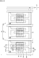
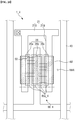
- FIG. 1 is a plan view illustrating a display device according to one embodiment.
- a display device 1 may include a plurality of pixels PX.
- Each pixel PX may include one or more light emitting elements 30, which emit light in a specific wavelength range, to display a specific color.
- Each pixel PX may include a first sub-pixel PX1, a second sub-pixel PX2, and a third sub-pixel PX3.
- the first sub-pixel PX1 may emit light of a first color
- the second sub-pixel PX2 may emit light of a second color
- the third sub-pixel PX3 may emit light of a third color.
- the first color may be a red color
- the second color may be a green color
- the third color may be a blue color, but the present invention is not limited thereto
- the sub-pixels PXn may emit light of the same color.
- each pixel PX has been illustrated as including three sub-pixels in FIG. 1 , the present invention is not limited thereto, and each pixel PX may include a larger number of sub-pixels.
- first, second, and the like are used to refer to each of the components, but these are used to simply distinguish the components from each other and do not necessarily refer to a corresponding component. That is, the components defined as first, second, and the like are not necessarily limited to a specific structure or location and, in some cases, other numbers may be assigned to the components. Therefore, the number assigned to each component may be described through the drawings and the following description, and a first component mentioned below may be a second component within the technical idea of the present invention.
- Each sub-pixel PXn of the display device 1 may include an area defined as an alignment area AA and an area defined as a non-alignment area NAA.
- the alignment area AA is defined as an area in which the light emitting elements 30 included in the display device 1 are disposed.
- the non-alignment area NAA may be an area other than the alignment area AA and defined as an area in which the light emitting elements 30 are not disposed and light is not emitted.
- the definition of the alignment area AA is not limited thereto and may be defined as an area in which the light emitting elements 30 should be disposed.
- the alignment area AA in which the light emitting elements 30 should be aligned is defined on each pixel PX or each sub-pixel PXn, and in the manufacturing process of the display device 1, the light emitting elements 30 may be disposed in the alignment area AA.
- the alignment area AA may include electrodes 21 and 22 of each sub-pixel PXn and may be defined as an area between the electrodes 21 and 22.
- the display device 1 includes a coating layer 80 disposed on at least a partial region of each pixel PX or each sub-pixel PXn.
- the coating layer 80 is disposed in the alignment area AA or the non-alignment area NAA of each sub-pixel PXn, and in some cases, the coating layer 80 may partially overlap the electrodes 21 and 22.
- FIG. 1 illustrates that the coating layer 80 is disposed in each sub-pixel PXn to entirely cover the electrodes 21 and 22 and includes an opening 80P which exposes some region of each sub-pixel PXn.
- the coating layer 80 may include the alignment area AA and may be partially disposed even in the non-alignment area NAA.
- the present invention is not limited thereto.
- the coating layer 80 distributes an ink S in which the light emitting elements 30 are dispersed to the electrodes 21 and 22 and applies an electric field to the ink S so that the light emitting elements 30 may be disposed on the electrodes 21 and 22.
- the coating layer 80 may perform a function of preventing the ink S sprayed on each pixel PX or each sub-pixel PXn from moving or spreading to an area other than a required alignment area AA. Owing to the coating layer 80, the ink S may be sprayed into the required alignment area AA, and the light emitting elements 30 may be smoothly disposed on the electrodes 21 and 22. A detailed description thereof will be made below.
- the sub-pixel PXn of the display device 1 may include a plurality of banks 40, a plurality of electrodes 21 and 22, the light emitting elements 30, and the coating layer 80.
- the plurality of electrodes 21 and 22 may be electrically connected to the light emitting elements 30 and may receive a predetermined voltage so as to allow the light emitting elements 30 to emit light.
- at least a portion of each of the electrodes 21 and 22 may be utilized to form an electric field in the sub-pixel PXn.
- the plurality of electrodes 21 and 22 may include a first electrode 21 and a second electrode 22.
- the first electrode 21 may be a pixel electrode which is separated in each sub-pixel PXn
- the second electrode 22 may be a common electrode which is commonly connected along the sub-pixels PXn.
- One of the first electrode 21 and the second electrode 22 may be an anode electrode of the light emitting element 30, and the other thereof may be a cathode electrode of the light emitting element 30.
- the present invention is not limited thereto and the reverse of the above description may be possible.
- the first electrode 21 and the second electrode 22 may include electrode stem portions 21S and 22S disposed to extend in a first direction D1 and include electrode branch portions 21B and 22B extending and branching from the electrode stem portions 21S and 22S in a second direction D2 intersecting the first direction D1.
- the first electrode 21 may include a first electrode stem portion 21S disposed to extend in the first direction D1, and at least one first electrode branch portion 21B branching from the first electrode stem portion 21S to extend in the second direction D2.
- first electrode stem portion 21S of any one pixel may be separated to be terminated between the sub-pixels PXn and disposed to be substantially collinear with a first electrode stem portion 21S of an adjacent sub-pixel PXn (e.g., a subpixel which is adjacent in the first direction D1) belonging to the same row.
- first electrode stem portion 21S disposed in each sub-pixel PXn may apply different electrical signals to first electrode branch portions 21B, and the first electrode branch portions 21B may be driven separately.
- the first electrode branch portion 21B branches from at least a portion of the first electrode stem portion 21S and is disposed to extend in the second direction D2.
- the first electrode branch portion 21B may be terminated in a state of being separated from the second electrode stem portion 22S which is disposed opposite to the first electrode stem portion 21S.
- the second electrode 22 may include the second electrode stem portion 22S which extends in the first direction D1 and is disposed to be separated from and opposite to the first electrode stem portion 21S, and the second electrode branch portion 22B which branches from the second electrode stem portion 22S and is disposed to extend in the second direction D2.
- one end portion of the second electrode stem portion 22S may extend to a plurality of adjacent sub-pixels PXn in the first direction D1.
- the two ends of the second electrode stem portion 22S of any one pixel may be connected to a second electrode stem portion 22S of an adjacent pixel PX among the pixels PX.
- the second electrode branch portion 22B may be separated from and opposite to the first electrode branch portion 21B and terminated in a state of being separated from the first electrode stem portion 21S. That is, one end portion of the second electrode branch portion 22B may be connected to the second electrode stem portion 22S, and the other end portion thereof may be disposed in the sub-pixel PXn in a state of being separated from the first electrode stem portion 21S.
- first electrode branch portions 21B have been illustrated as being disposed and the second electrode branch portion 22B has been illustrated as being disposed between the two first electrode branch portions 21B, but the present invention is not limited thereto.
- the plurality of banks 40 may include a third bank 43 disposed at a boundary between the sub-pixels PXn, and a first bank 41 and a second bank 42 which are disposed below the electrodes 21 and 22. Although the first bank 41 and the second bank 42 are not illustrated in the drawing, the first bank 41 and the second bank 42 may be disposed below the first electrode branch portion 21B and the second electrode branch portion 22B, respectively.
- the third bank 43 may be disposed at a boundary between the sub-pixels PXn. End portions of the plurality of first electrode stem portions 21S may be separated from each other to be terminated based on the third bank 43.
- the third bank 43 may extend in the second direction D2 and may be disposed at the boundary between the sub-pixels PXn disposed in the first direction D1. However, the present invention is not limited thereto, and the third bank 43 may extend in the first direction D1 and may be disposed even at the boundary between the sub-pixel PXn disposed in the second direction D2.
- the third bank 43 may include the same material as the first bank 41 and the second bank 42 and may be formed in substantially the same process.
- a first insulating layer 51 may be disposed in each sub-pixel PXn to entirely cover each sub-pixel PXn including the first electrode branch portion 21B and the second electrode branch portion 22B.
- the first insulating layer 51 may protect each of the electrodes 21 and 22 and, simultaneously, insulate the electrodes 21 and 22 from each other so as not to be in direct contact with each other.
- the plurality of light emitting elements 30 may be disposed between the first electrode branch portion 21B and the second electrode branch portion 22B. One end portions of at least some of the plurality of light emitting elements 30 may be electrically connected to the first electrode branch portion 21B and the other end portions thereof electrically connected to the second electrode branch portion 22B.
- the plurality of light emitting elements 30 may be separated from each other in the second direction D2 and disposed substantially parallel to each other.
- a separation gap between the light emitting elements 30 is not particularly limited.
- the plurality of light emitting elements 30 may be disposed adjacent to each other to form a group, and a plurality of other light emitting elements 30 may be grouped in a state of being spaced at regular intervals from each other, may have a nonuniform density, and may be oriented and aligned in one direction.
- the contact electrode 26 may be disposed on the first electrode branch portion 21B and the second electrode branch portion 22B. However, the contact electrode 26 may be substantially disposed on the first insulating layer 51, and at least a portion of the contact electrode 26 may be in contact with or electrically connected to the first electrode branch portion 21B and the second electrode branch portion 22B.
- a plurality of contact electrodes 26 may be disposed to extend in the second direction D2 and disposed to be separated from each other in the first direction D1.
- the contact electrode 26 may be in contact with at least one end portion of the light emitting element 30, and the contact electrode 26 may be in contact with the first electrode 21 or the second electrode 22 to receive an electrical signal.
- the contact electrode 26 may transmit an electrical signal, which is transmitted from each of the electrodes 21 and 22, to the light emitting element 30.
- the contact electrode 26 may include a first contact electrode 26a and a second contact electrode 26b.
- the first contact electrode 26a may be disposed on the first electrode branch portion 21B to be in contact with one end portion of the light emitting element 30, and the second contact electrode 26b may be disposed on the second electrode branch portion 22B to be in contact with the other end portion thereof.
- the first electrode stem portion 21S and the second electrode stem portion 22S may be electrically connected to a circuit element layer of the display device 1 through contact holes, for example, a first electrode contact hole CNTD and a second electrode contact hole CNTS.
- contact holes for example, a first electrode contact hole CNTD and a second electrode contact hole CNTS.
- one second electrode contact hole CNTS has been illustrated as being formed in the second electrode stem portion 22S of each of the plurality of sub-pixels PXn.
- the present invention is not limited thereto, and in some cases, the second electrode contact hole CNTD may be formed in each sub-pixel PXn.
- the display device 1 may include a second insulating layer 52 (see FIG. 10 ) and a passivation layer 55 (see FIG. 10 ) which are disposed to cover at least a portion of each of the electrodes 21 and 22 and the light emitting element 30. An arrangement and structures thereof will be described below.
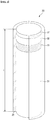
- FIG. 2 is a schematic diagram illustrating the light emitting element 30 according to one embodiment.
- the light emitting element 30 may be an LED.
- the light emitting element 30 may be an inorganic LED having a micrometer unit or nanometer unit size and made of an inorganic material.
- the inorganic light emitting diode may be aligned between two electrodes in which polarity is formed by forming an electric field in a specific direction between the two electrodes facing each other.
- the light emitting element 30 may be aligned between two electrodes due to an electric field formed on the two electrodes.
- the light emitting element 30 may include a semiconductor crystal doped with an arbitrary conductivity type (e.g., p-type or n-type) impurity.
- the semiconductor crystal may receive an electrical signal applied from an external power source and emit light in a specific wavelength range.
- the light emitting element 30 may include a first conductivity type semiconductor 31, a second conductivity type semiconductor 32, an active layer 33, and an insulating film 38.
- the light emitting element 30 may further include at least one conductive electrode layer 37.
- the light emitting element 30 has been illustrated as further including one conductive electrode layer 37 in FIG. 2 , the present invention is not limited thereto. In some cases, the light emitting element 30 may include a greater number of conductive electrode layers 37 or the conductive electrode layer 37 may be omitted. A description of the light emitting element 30, which will be made below, may be identically applied even when the number of conductive electrode layers 37 is varied or another structure is further included.
- the light emitting element 30 may have a shape extending in one direction.
- the light emitting element 30 may have a shape of nanorods, nanowires, nanotubes, or the like.
- the light emitting element 30 may be a cylindrical shape or a rod shape.
- the shape of the light emitting element 30 is not limited thereto and may have various shapes such as a regular hexahedral shape, a rectangular parallelepiped shape, a hexagonal column shape, and the like.
- a plurality of semiconductors included in the light emitting element 30, which will be described below, may have a structure in which the semiconductors are sequentially disposed or stacked in the one direction.
- the light emitting element 30 may emit light in a specific wavelength range.
- the active layer 33 may emit blue light having a central wavelength range ranging from 450 nm to 495 nm.
- the central wavelength range of the blue light is not limited to the above range, and it should be understood that the central wavelength range includes all wavelength ranges which can be recognized as a blue color in the art.
- the light emitted from the active layer 33 of the light emitting element 30 is not limited thereto, and the light may be green light having a central wavelength range ranging from 495 nm to 570 nm or red light having a central wavelength range ranging from 620 nm to 750 nm.
- the first conductivity type semiconductor 31 may be an n-type semiconductor having, for example, a first conductivity type.
- the first conductivity type semiconductor 31 may include a semiconductor material having a chemical formula of In x Al y Ga 1-x-y N (0 ⁇ x ⁇ 1, 0 ⁇ y ⁇ 1, and 0 ⁇ x+y ⁇ 1).
- the semiconductor material may be one or more among InAlGaN, GaN, AlGaN, InGaN, AlN, and InN which are doped with an n-type impurity.
- the first conductivity type semiconductor 31' may be doped with a first conductive dopant.
- the first conductivity type dopant may be Si, Ge, Sn, or the like.
- the first conductivity type semiconductor 31 may be n-GaN doped with n-type Si.
- a length of the first conductivity type semiconductor 31 may range from 1.5 ⁇ m to 5 ⁇ m, but the present invention is not limited thereto.
- the second conductivity type semiconductor 32 is disposed on the active layer 33 which will be described below.
- the second conductivity type semiconductor 32 may be a p-type semiconductor having a second conductivity type.
- the second conductivity type semiconductor 32 may include a semiconductor material having a chemical formula of In x Al y Ga 1-x-y N(0 ⁇ x ⁇ 1, 0 ⁇ y ⁇ 1, and 0 ⁇ x+y ⁇ 1).
- the semiconductor material may be one or more among InAlGaN, GaN, AlGaNN, InGaN, AlN, and InN which are doped with a p-type impurity.
- the second conductivity type semiconductor 32 may be doped with a second conductive dopant.
- the second conductive dopant may be Mg, Zn, Ca, Se, Ba, or the like.
- the second conductivity type semiconductor 32 may be p-GaN doped with p-type Mg.
- a length of the second conductivity type semiconductor 32 may range from 0.08 ⁇ m to 0.25 ⁇ m, but the present invention is not limited thereto.
- each of the first conductivity type semiconductor 31 and the second conductivity type semiconductor 32 has been illustrated as being formed as one layer, the present invention is not limited thereto.
- each of the first conductivity type semiconductor 31 and the second conductivity type semiconductor 32 may further include a larger number of layers, for example, a clad layer or a tensile strain barrier reducing (TSBR) layer according to a material of the active layer 33.
- TSBR tensile strain barrier reducing
- the active layer 33 is disposed between the first conductivity type semiconductor 31 and the second conductivity type semiconductor 32.
- the active layer 33 may include a material having a single or multiple quantum well structure.
- the active layer 330 may have a structure in which a plurality of quantum layers and a plurality of well layers are alternately stacked.
- the active layer 33 may emit light due to a combination of electron-hole pairs in response to an electrical signal applied through the first conductivity type semiconductor 31 and the second conductivity type semiconductor 32.
- the active layer 33 may include a material such as AlGaN, AlInGaN, or the like.
- the active layer 33 when the active layer 33 has a multi-quantum well structure in which quantum layers and well layers are alternately stacked, the quantum layer may include a material such as AlGaN or AlInGaN, and the well layer may include a material such as GaN or AlInN.
- the active layer 33 includes AlGaInN as the quantum layer and AlInN as the well layer.
- the active layer 33 may emit blue light having a central wavelength range ranging from 450 nm to 495 nm.
- the active layer 33 may have a structure in which a semiconductor material having large band gap energy and a semiconductor material having small band gap energy are alternately stacked or include different Group III to V semiconductor materials according to a wavelength range of emitted light.
- the active layer 33 is not limited to emit light in the blue wavelength range, and in some cases, the active layer 33 may emit light in a red or green wavelength range.
- a length of the active layer 33 may range from 0.05 ⁇ m to 0.25 ⁇ m, but the present invention is not limited thereto.
- the light emitted from the active layer 33 may be emitted to an outer surface of the light emitting element 30 in a length direction and both side surfaces thereof. Directivity of the light emitted from the active layer 33 is not limited in one direction.
- the conductive electrode layer 37 may be an ohmic contact electrode. However, the present invention is not limited thereto, and the conductive electrode layer 37 may be a Schottky contact electrode.
- the conductive electrode layer 37 may include a conductive metal.
- the conductive electrode layer 37 may include at least one among aluminium (Al), titanium (Ti), indium (In), gold (Au), silver (Ag), indium tin oxide (ITO), indium zinc oxide (IZO), and indium tin-zinc oxide (ITZO).
- the conductive electrode layer 37 may include a semiconductor material doped with an n-type or p-type impurity.
- the conductive electrode layer 37 may include the same material or different materials, but the present invention is not limited thereto.
- the insulating film 38 is disposed to surround the outer surfaces of the plurality of semiconductors which are described above.
- the insulating film 38 may be disposed to surround at least the outer surface of the active layer 33 and may extend in one direction in which the light emitting element 30 extends.
- the insulating film 38 may serve to protect the members.
- the insulating film 38 may be formed to surround side surfaces of the members and to expose the both end portions of the light emitting element 30 in the length direction.
- the insulating film 38 has been illustrated as being formed to extend in the length direction of the light emitting element 30 to cover from the first conductivity type semiconductor 31 to the conductive electrode layer 37, but the present invention in not limited thereto.
- the insulating film 38 covers only the outer surfaces of some semiconductor layers including the active layer 33 or covers only a portion of the outer surface of the conductive electrode layer 37 so that a portion of the outer surface of the conductive electrode layer 37 may be exposed.
- a thickness of the insulating film 38 may range from 10 nm to 1.0 ⁇ m, but the present invention is not limited thereto. Preferably, the thickness of the insulating film 38 may be 40 nm.
- the insulating film 38 may include materials having insulation properties, for example, silicon oxide (SiO x ), silicon nitride (SiN x ), silicon oxynitride (SiO x N y ), aluminium nitride (AlN), aluminium oxide (Al 2 O 3 ), and the like.
- silicon oxide (SiO x ) silicon nitride (SiN x ), silicon oxynitride (SiO x N y ), aluminium nitride (AlN), aluminium oxide (Al 2 O 3 ), and the like.
- the outer surface of the insulating film 38 may be surface treated.
- the light emitting element 30 may be sprayed onto an electrode in a state of being dispersed in a predetermined ink to be aligned.
- the insulating film 38 may be hydrophobically or hydrophilically treated.
- the light emitting element 30 may have a length 1 ranging from 1 ⁇ m to 10 ⁇ m or from 2 ⁇ m to 5 ⁇ m, and preferably, have the length 1 of about 4 ⁇ m.
- a diameter of the light emitting element 30 may range from 300 nm to 700 nm, and an aspect ratio of the light emitting element 30 may range from 1.2 to 100.
- the present invention is not limited thereto, and the plurality of light emitting elements 30 included in the display device 1 may have different diameters according to a difference in composition of the active layers 33.
- the diameter of the light emitting element 30 may be about 500 nm.
- the light emitting elements 30 may be sprayed onto the electrodes 21 and 22 in a state of being dispersed in the ink S.
- the ink S it is required for the ink S to be located in the required alignment area AA.
- the coating layer 80 disposed in at least a partial region of the pixel PX or the sub-pixel PXn may be formed, thereby preventing the ink S in which the light emitting elements 30 are dispersed from spreading from the alignment area AA.
- FIG. 3 is a schematic cross-sectional view illustrating the display device according to one embodiment.
- the coating layer 80 may be disposed to entirely cover a target substrate SUB and the electrodes 21 and 22.
- the light emitting element 30 may be disposed on the coating layer 80 between the first electrode 21 and the second electrode 22.
- the coating layer 80 disposed on the electrodes 21 and 22 may prevent the spread of the sprayed ink S to induce the light emitting element 30 to be disposed in the alignment area AA defined on the target substrate SUB.
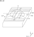
- FIG. 4 is a schematic diagram illustrating that an ink is sprayed onto an electrode according to Comparative Example.
- FIG. 5 is a cross-sectional view taken along line IIa-IIa' of FIG. 4 .
- the ink S in which the light emitting elements 30 are dispersed may be sprayed onto the target substrate SUB.
- the alignment area AA and a non-alignment area NAA are defined on the target substrate SUB, and the ink S is sprayed onto the electrodes 21 and 22 in the alignment area AA.
- the coating layer 80 is not formed on the target substrate SUB, the ink S sprayed onto the target substrate SUB moves in at least one direction, and particularly, the ink S deviates from the alignment area AA to spread to the non-alignment area NAA.
- the coating layer 80 is formed before the ink S is sprayed so that the ink S may be prevented from moving to an area other than the alignment area AA. That is, the display device 1 may include the coating layer 80 which performs a function of preventing spreading of ink S to induce the light emitting elements 30 to be smoothly disposed in the alignment area AA.
- FIG. 6 is a schematic diagram illustrating that an ink is sprayed onto an electrode on which a coating layer is formed according to one embodiment.
- FIG. 7 is a cross-sectional view taken along line IIb-IIb' of FIG. 6 .
- the display device 1 may include the coating layer 80 disposed on the target substrate SUB, for example, disposed to cover the first electrode 21 and the second electrode 22.
- the ink S in which the light emitting elements 30 are dispersed may be sprayed onto the coating layer 80 in the alignment area AA.
- the coating layer 80 may prevent the sprayed ink S from moving in at least one direction.
- the ink S sprayed onto the coating layer 80 may not spread in one direction and may be maintained at an initial sprayed position, and among the light emitting elements 30 dispersed in the ink S, occupation of light emitting elements 30 located in the alignment area AA may be increased.
- most of the light emitting elements 30 dispersed in the ink S may be disposed between the electrodes 21 and 22 in the alignment area AA.
- the spreading prevention function of the coating layer 80 may be induced by controlling a contact angle ⁇ d using a difference in surface energy between the coating layer 80 and a solvent of the ink S.
- the ink S in which the light emitting elements 30 are dispersed may include a solvent having a first polarity, and at least a partial region of the coating layer 80 may include a material having a second polarity opposite to the first polarity.
- the ink S sprayed onto the target substrate SUB may form a predetermined contact angle ⁇ d on an interface with the target substrate SUB or the coating layer 80.
- a liquid sprayed onto a target object may have a shape which minimizes surface energy of a surface of the liquid.
- the ink S sprayed onto the target substrate SUB or the coating layer 80 may have a spherical or semi-elliptical shape which minimizes surface energy on a surface of the ink S.
- surface energy may be formed on interfaces between the ink S and the target substrate SUB or the coating layer 80, between air and the target substrate SUB or the coating layer 80, and between the air and the ink S in one directions.
- first surface energy ySL is formed on the interface between the ink S and the target substrate SUB
- a second surface energy ySV is formed on the interface between the target substrate SUB and the air
- third surface energy yLV is formed on the interface between the ink S and air.
- ySL is the first surface energy
- ySV is the second surface energy
- yLV is the third surface energy
- ⁇ d is the contact angle between the surface of the ink S and the target substrate SUB
- the ink S when an ySL value which is the first surface energy is smaller than an ySV value which is the third surface energy, the ink S may exhibit a behavior so as to minimize surface energy of the interface. That is, a force is applied to the ink S at a point at which the ink S is in contact with the target substrate SUB in one direction of a transverse direction in which the third surface energy ySV having a large value is applied, and the surface of the ink S may move in the one direction. Thus, the contact angle ⁇ d between the ink S and the target substrate SUB is decreased, and the ink S spreads in the one direction on the target substrate SUB.
- the coating layer 80 may control a difference between the first surface energy ySL and the third surface energy ySV from the ink S.
- the ink S may be sprayed onto the coating layer 80, and thus the first surface energy ySL may have a value greater than a value of the third surface energy ySV on the interface between the coating layer 80 and the ink S.
- the force acts in a direction to which the first surface energy ySL is directed so that the coating layer 80 may induce the surface energy of the ink S to have a small value and may prevent the ink S from spreading.
- the coating layer 80 includes a material having a polarity opposite to a polarity of the solvent of ink S, and thus the first surface energy ySL and the contact angle ⁇ d between the coating layer 80 and the ink S may each have a large value.
- the coating layer 80 may prevent the ink S sprayed on the alignment area AA from spreading to the non-alignment area NAA.
- the solvent of the ink S may be hydrophilic, and at least a portion of the coating layer 80 may include a hydrophobic material.
- the contact angle ⁇ d between the coating layer 80 and the ink S may have a value of 30° or more.
- the hydrophobic material may be a polymer including fluorine (F).
- the coating layer 80 may include 1H,1H,2H,2H-perfluorodecyltrichlorosilane.
- the material included in the coating layer 80 is not limited thereto.
- the coating layer 80 may include a hydrophilic material.
- some regions of the coating layer 80 may have the same polarity as the ink S, and the remaining regions of the coating layer 80 may have a polarity opposite to a polarity of the ink S.
- a structure and a material of the coating layer 80 are not limited.
- the coating layer 80 may include a first region and a second region which have different polarities, and the ink S may be sprayed between the first and second regions.
- the coating layer 80 may prevent the ink S from moving to the second region. That is, it is possible to prevent the ink S from spreading from the first region to the second region on the coating layer 80. A description thereof will be made below with reference to other drawings.
- the display device 1 may further include a contact electrode 26 in contact with the light emitting element 30 and the electrodes 21 and 22.
- the contact electrode 26 may be in contact with at least one end portion of the light emitting element 30 and may be in contact with regions of the electrodes 21 and 22 in which the coating layer 80 is partially removed to be exposed.
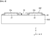
- FIGS. 8 and 9 are schematic cross-sectional views illustrating a display device according to another embodiment.
- the coating layer 80 may include the opening 80P which exposes at least a portion of each of the electrodes 21 and 22 and may further include the contact electrode 26 in contact with the electrodes 21 and 22 which are exposed through the opening 80P.
- the coating layer 80 may be disposed to cover the electrodes 21 and 22, and the opening 80P may overlap the electrodes 21 and 22 to expose a partial region of each of the electrodes 21 and 22.
- An area in which the opening 80P is disposed may be an area in which the coating layer 80 partially exposes upper surfaces of the electrodes 21 and 22 in FIG. 1 .
- the opening 80P may partially expose the upper surfaces of the electrodes 21 and 22, but the present invention is not limited thereto.
- the opening 80P may entirely expose flat upper surfaces of the electrodes 21 and 22 and may partially expose inclined side surfaces of the electrodes 21 and 22.
- the contact electrode 26 is disposed on the electrodes 21 and 22.
- the contact electrode 26 may be in contact with the light emitting element 30 and the regions of the electrodes 21 and 22 which are exposed through the opening 80P.
- the contact electrode 26 includes a first contact electrode 26a disposed on the first electrode 21 and a second contact electrode 26b disposed on the second electrode 22.
- the first contact electrode 26a may be in contact with the exposed region of the first electrode 21 and one end portion of the light emitting element 30, and the second contact electrode 26b may be contact with the exposed region of the second electrode 22 and the other end portion of the light emitting element 30.
- the coating layer 80 may be formed to entirely cover the target substrate SUB and the electrodes 21 and 22 to dispose the light emitting element 30 in the alignment area AA, and the opening 80P may be formed to expose a portion of each of the electrodes 21 and 22. Even when the coating layer 80 entirely covers the electrodes 21 and 22, since the display device 1 further includes the contact electrode 26 in contact with the light emitting element 30 and the electrodes 21 and 22 exposed through the opening 80P, electrical signals transmitted from the electrodes 21 and 22 may be transmitted to the light emitting element 30 through the contact electrode 26.
- the opening 80P of the coating layer 80 may expose at least a portion of a side surface, including the upper surface, of each of the electrodes 21 and 22. Areas of the electrodes 21 and 22 exposed by the opening 80P are increased, and the contact electrode 26 may be in contact with the electrodes 21 and 22 in a larger region. Thus, contact resistance between the contact electrode 26 and the electrodes 21 and 22 may be reduced.
- the structure of the display device 1 is not limited thereto, and the display device 1 may have a structure different from the above structure or a larger number of members may be disposed on the target substrate SUB. A description thereof will be made with reference to other drawings.
- FIG. 10 is a partial cross-sectional view taken along line I-I' of FIG. 1 .
- FIG. 10 illustrates the cross-sectional view of the first sub-pixel PX1 and may be equally applied to other pixels PX or other sub-pixels PXn.
- FIG. 6 illustrates a cross section crossing one end portion and the other end portion of an arbitrary light emitting element 30.
- the display device 1 may further include a circuit element layer located below the electrodes 21 and 22.
- the circuit element layer may include a plurality of semiconductor layers and a plurality of conductive patterns and may include at least one transistor and a power line. However, a detailed description thereof will be omitted below.
- the display device 1 may include a via layer 20, the electrodes 21 and 22 disposed on the via layer 20, and the light emitting element 30.
- a circuit element layer (not shown) may be further disposed below the via layer 20.
- the via layer 20 may include an organic insulating material and perform a surface planarization function.
- a plurality of banks 41, 42, and 43 are disposed on the via layer 20.
- the plurality of banks 41, 42, and 43 may be disposed to be separated from each other in each sub-pixel PXn.
- the plurality of banks 41, 42, and 43 may include the first bank 41 and the second bank 42 which are disposed adjacent to a central portion of the sub-pixel PXn, and the third bank 43 disposed at a boundary between the sub-pixels PXn.
- the third bank 43 may perform a function of blocking the ink I from crossing the boundary of the sub-pixel PXn.
- the display device 1 further includes other members, the other members may be disposed on the third bank 43, and the third bank 43 may perform a function of supporting the other members.
- the present invention is not limited thereto.
- the first bank 41 and the second bank 42 are disposed to be separated from and opposite to each other.
- the first electrode 21 may be disposed on the first bank 41, and the second electrode 22 may be disposed on the second bank 42. Referring to FIGS. 2 and 6 , it can be understood that the first electrode branch portion 21B is disposed on the first bank 41, and the second bank 42 is disposed on the second bank 42.
- the first bank 41, the second bank 42, and the third bank 43 may be formed substantially in the same process.
- the banks 41, 42, and 43 may constitute a single grid pattern.
- Each of the plurality of banks 41, 42, and 43 may include polyimide (PI).
- Each of the plurality of banks 41, 42, and 43 may have a structure in which at least a portion protrudes from the via layer 20.
- the banks 41, 42, and 43 may protrude upward from a flat surface on which the light emitting element 30 is disposed, and at least a part of each of the protruding portions may have a slope.
- a shape of each of the banks 41, 42, and 43 having the protruding structures is not particularly limited. As shown in the drawing, the first bank 41 and the second bank 42 protrude to the same height, and the third bank 43 may have a shape protruding to a higher position.
- Reflective layers 21a and 22a may be disposed on the first bank 41 and the second bank 42, and electrode layers 21b and 22b may be disposed on the reflective layers 21a and 22a.
- the reflective layers 21a and 22a and the electrode layers 21b and 22b may constitute the electrodes 21 and 22.
- the reflective layers 21a and 22a include a first reflective layer 21a and a second reflective layer 22a.
- the first reflective layer 21a may cover the first bank 41
- the second reflective layer 22a may cover the second bank 42. Portions of the reflective layers 21a and 22a are electrically connected to the circuit element layer through a contact hole passing through the via layer 20.
- Each of the reflective layers 21a and 22a may include a material having high reflectance to reflect light emitted from the light emitting element 30.
- each of the reflective layers 21a and 22a may include a material such as Ag, Cu, ITO, IZO, or ITZO, but the present invention is not limited thereto.
- the electrode layers 21b and 22b include a first electrode layer 21b and a second electrode layer 22b.
- the electrode layers 21b and 22b may have patterns substantially equal to patterns of the reflective layers 21a and 22a.
- the first reflective layer 21a and the first electrode layer 21b are disposed to be separated from the second reflective layer 22a and the second electrode layer 22b.
- Each of the electrode layers 21b and 22b includes a transparent conductive material, and thus light emitted from the light emitting element 30 may be incident on the reflective layers 21a and 22a.
- each of the electrode layers 21b and 22b may include a material such as ITO, IZO, or ITZO, but the present invention is not limited thereto.
- the reflective layers 21a and 22a and the electrode layers 21b and 22b may form a structure in which one or more transparent conductive layers such as ITO, IZO, or ITZO, and one or more metal layers such as Ag or Cu are stacked.
- the reflective layers 21a and 22a and the electrode layers 21b and 22b may form a stacked structure of ITO/Ag/ITO/IZO.
- the first electrode 21 and the second electrode 22 may be formed as a single layer. That is, the reflective layers 21a and 22a and the electrode layers 21b and 22b may be formed as a single layer to transmit an electrical signal to the light emitting element 30 and, simultaneously, reflect light.
- each of the first electrode 21 and the second electrode 22 may include a conductive material having high reflectance and may be an alloy containing Al, nickel (Ni), and lanthanum (La).
- the present invention is not limited thereto.
- the first insulating layer 51 is disposed to partially cover the first electrode 21 and the second electrode 22.
- the first insulating layer 51 may be disposed to cover most of upper surfaces of the first electrode 21 and the second electrode 22 and may expose portions of the first electrode 21 and the second electrode 22.
- the first insulating layer 51 may be disposed to partially cover an area in which the first electrode 21 is separated from the second electrode 22 and an area opposite to the area in which the first electrode 21 is separated from the second electrode 22.
- the first insulating layer 51 is disposed to expose relatively flat upper surfaces of the first electrode 21 and the second electrode 22 and disposed to allow the electrodes 21 and 22 to overlap inclined surfaces of the first bank 41 and the second bank 42.
- the first insulating layer 51 forms a flat upper surface to allow the light emitting element 30 to be disposed, and the flat upper surface extends toward the first electrode 21 and the second electrode 22 in one direction.
- the extension portion of the first insulating layer 51 is terminated at inclined surfaces of the first electrode 21 and the second electrode 22.
- the contact electrodes 26 may be in contact with the exposed first electrode 21 and the exposed second electrode 22 and may be in smooth contact with the light emitting element 30 on the flat upper surface of the first insulating layer 51.
- the first insulating layer 51 may protect the first electrode 21 and the second electrode 22 and, simultaneously, insulate the first electrode 21 from the second electrode 22. In addition, the first insulating layer 51 may prevent the light emitting element 30 disposed thereon from being damaged by direct contact with other members.
- the coating layer 80 may be disposed on the first insulating layer 51.
- the coating layer 80 may have substantially the same shape as the first insulating layer 51 in a cross section. The above shape may be formed such that a material constituting the first insulating layer 51 and a material constituting the coating layer 80 are sequentially disposed on the electrodes 21 and 22 in the manufacturing process of the display device 1 and then etched in the same process.
- the opening 80P of the coating layer 80 may be formed in a region in which the first insulating layer 51 and the coating layer 80 are etched, thereby exposing some regions of the electrodes 21 and 22. Some regions of the electrodes 21 and 22 exposed through the opening 80P may be in contact with the contact electrode 26 which will be described below.
- the present invention is not limited thereto, and the coating layer 80 may be disposed in only a partial region on the first insulating layer 51 so that the coating layer 80 and the first insulating layer 51 may have different shapes.
- a description of the coating layer 80 is the same as the above description, and thus a detailed description thereof will be omitted herein.
- various examples of the coating layer 80 will be described below with reference to other drawings.
- the light emitting element 30 may be disposed on the coating layer 80 or the first insulating layer 51. In the drawing, the light emitting element 30 is shown as being disposed on the coating layer 80 which is disposed on the first insulating layer 51. At least one light emitting element 30 may be disposed on the coating layer 80 between the first electrode 21 and the second electrode 22.
- the light emitting element 30 may include a plurality of layers disposed in a direction horizontal to the via layer 20.
- the light emitting element 30 of the display device 1 may include the conductive semiconductors and the active layer, which are described above, and the conductive semiconductors and the active layer may be sequentially disposed on the via layer 20 in the transverse direction.
- the first conductivity type semiconductor 31, the active layer 33, the second conductivity type semiconductor 32, and the conductive electrode layer 37 may be sequentially disposed on the via layer 20 in the horizontal direction.
- the present invention is not limited thereto.
- the order of the plurality of layers disposed in the light emitting element 30 may be the opposite. In some cases, when the light emitting element 30 has another structure, the plurality of layers may be disposed in a direction perpendicular to the via layer 20.
- the second insulating layer 52 may be partially disposed on the light emitting element 30.
- the second insulating layer 52 may protect the light emitting element 30 and, simultaneously, perform a function of fixing the light emitting element 30 during a process of manufacturing the display device 1.
- the second insulating layer 52 may be disposed to surround an outer surface of the light emitting element 30. That is, a portion of a material of the second insulating layer 52 may be disposed between a bottom surface of the light emitting element 30 and the first insulating layer 51.
- the second insulating layer 52 may extend between the first electrode branch portion 21B and the second electrode branch portion 22B in the second direction D2 to have an island shape or a linear shape when viewed in a plan view.
- the contact electrodes 26 are disposed on the electrodes 21 and 22 and the second insulating layer 52.
- the first contact electrode 26a and the second contact electrode 26b are disposed to be spaced apart from each other on the second insulating layer 52.
- the second insulating layer 52 may insulate the first contact electrode 26a from the second contact electrode 26b.
- the first contact electrode 26a may be in contact with at least the first electrode 21, which is exposed due to patterning of the first insulating layer 51 and the coating layer 80 and may be in contact with one end portion of the light emitting element 30.
- the second contact electrode 26b may be in contact with at least the second electrode 22, which is exposed due to the patterning of the first insulating layer 51 and the coating layer 80 and may be in contact with the other end portion of the light emitting element 30.
- the first and second contact electrodes 26a and 26b may be in contact with side surfaces of the two end portions of the light emitting element 30, for example, the first conductivity type semiconductor 31, the second conductivity type semiconductor 32, or the conductive electrode layer 37.
- the first insulating layer 51 forms the flat upper surface so that the contact electrodes 26 may be in smooth contact with the side surfaces of the light emitting element 30.
- the contact electrode 26 may include a conductive material.
- the contact electrode 260 may include ITO, IZO, ITZO, Al, or the like.
- the present invention is not limited thereto.
- the passivation layer 55 is disposed above the second insulating layer 52 and the contact electrode 26.
- the passivation layer 55 may serve to protect members disposed on the via layer 20 from an external environment.
- Each of the first insulating layer 51, the second insulating layer 52, and the passivation layer 55 may include an inorganic insulating material or an organic insulating material.
- each of the first insulating layer 51, the second insulating layer 52, and the passivation layer 55 may include a material such as SiO x , SiN x , SiO x N y , Al 2 O 3 , aluminium nitride (AlN), or the like.
- the second insulating layer 52 may be made of an organic insulating material including a photoresist or the like. However, the present invention is not limited thereto.
- FIG. 11 is a flowchart illustrating a method of manufacturing a display device according to one embodiment.
- the method of manufacturing the display device 1 includes preparing a target substrate SUB and the first electrode 21 and the second electrode 22 which are disposed on the target substrate SUB (S100), forming the coating layer 80 disposed on at least a partial region of the target substrate SUB and configured to cover at least a portion of each of the first electrode 21 and the second electrode 22 (S200), and spraying the ink S including the light emitting elements 30 onto the coating layer 80 which covers the first electrode 21 and the second electrode 22 and landing the light emitting elements 30 between the first electrode 21 and the second electrode 22 (S300).
- the method of manufacturing the display device 1 may include preparing the first electrode 21 and the second electrode 22 which are disposed on the target substrate SUB, forming the coating layer 80 disposed on at least a partial region of the target substrate SUB, and then landing the light emitting elements 30 between the first electrode 21 and the second electrode 22.
- the coating layer 80 may be disposed to partially overlap the electrodes 21 and 22 on the target substrate SUB, but the present invention is not limited thereto. In some cases, the coating layer 80 may be disposed only in a region other than the first electrode 21 and the second electrode 22.
- the coating layer 80 entirely covers, including the first electrode 21 and the second electrode 22, the target substrate SUB will be described.
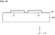
- FIGS. 12 to 16 are cross-sectional views illustrating processes of the method of manufacturing a display device according to one embodiment.
- the target substrate SUB on which the first electrode 21 and the second electrode 22 are formed is prepared (S100).
- S100 the target substrate SUB on which the first electrode 21 and the second electrode 22 are formed.
- the display device 1 is not limited thereto, and as described above, the display device 1 may include more members such as the bank 40, the contact electrode 26, and the like.
- the coating layer 80 is formed to be disposed on the target substrate SUB and the electrodes 21 and 22 (S200).
- a method of forming the coating layer 80 is not particularly limited.
- the coating layer 80 may include a self-assembly monolayer and may be formed on the electrodes 21 and 22.
- the present invention is not limited thereto.
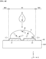
- the ink S including the light emitting element 30 is sprayed onto the first electrode 21 and the second electrode 22.
- the ink S may be disposed on the coating layer 80 which is disposed to cover the first electrode 21 and the second electrode 22.
- the ink S may include a solvent and a plurality of light emitting elements 30 included in the solvent.
- the ink S may be provided in a solution or colloidal state.
- the solvent may be acetone, water, alcohol, toluene, propylene glycol (PG), or propylene glycol methyl acetate (PGMA), but the present invention is not limited thereto.
- ink S may include hydrophilic PG as a solvent, and the coating layer 80 may include a hydrophobic fluorine-based polymer. That is, the ink S and the coating layer 80 may include materials having opposite polarities.
- the first surface energy ySL (not shown) formed on the interface between the coating layer 80 and the ink S has a large value
- the contact angle ⁇ d between the ink S and the coating layer 80 has a large value.
- the ink S sprayed on the coating layer 80 may be maintain at a first sprayed position without spreading in one direction.
- the ink S is sprayed in the alignment area AA defined on the first electrode 21 and the second electrode 22, and thus a large number of light emitting elements 30 may be located in the alignment area AA.
- the light emitting element 30 is landed between the first electrode 21 and the second electrode 22 (S300).
- the landing of the light emitting element 30 (S300) may include applying an electrical signal to the first electrode 21 and the second electrode 22 and forming an electric field in the ink S, applying a dielectrophoretic force to the light emitting element 30 due to the electric field and landing the light emitting element 30 on the electrodes 21 and 22, and removing the solvent of the ink S.
- the light emitting element 30 may be disposed on the electrodes 21 and 22 using dielectrophoresis (DEP).
- DEP dielectrophoresis
- the solution in which the light emitting elements 30 are dispersed is sprayed onto the electrodes 21 and 22, and alternating-current (AC) power is applied to the electrodes 21 and 22.
- AC alternating-current
- the AC power is applied to the first electrode 21 and the second electrode 22
- an electric field is generated between the first electrode 21 and the second electrode 22
- the light emitting element 30 receiving a dielectrophoretic force due to the electric field may be disposed on the electrodes 21 and 22.
- an electric field E may be formed in the ink S sprayed onto the electrodes 21 and 22.
- the electric field E may apply a dielectrophoretic force to the light emitting element 30, and the light emitting element 30 receiving the dielectrophoretic force may be landed on the first electrode 21 and the second electrode 22.
- the solvent of the ink S is removed.
- the removing of the solvent may employ a conventional method.
- the solvent may be removed through a method such as a heat treatment method, an infrared irradiation method, or the like.
- the display device 1 including the coating layer 80 may be manufactured through the above processes.
- the method of manufacturing the display device 1 is not limited thereto. As described above, the display device 1 may include a larger number of members, and thus more processes may be performed. A detailed description thereof will be omitted herein.
- FIGS. 17 to 20 are plan views illustrating the display device according to another embodiment.
- a display device 1_1 may be formed such that a coating layer 80_1 substantially overlaps the alignment area AA.
- the coating layer 80_1 may be formed in a relatively narrow area when compared with the display device 1 of FIG. 1 .
- a duplicate description will be omitted and a description will be made to focus on a difference.
- the coating layer 80_1 of the display device 1_1 may be disposed to overlap only an alignment area AA in which light emitting elements 30 are aligned.
- boundaries of the alignment area AA and the coating layer 80_1 have been illustrated as being spaced apart from each other, but the coating layer 80_1 may overlap the alignment area AA.
- a first electrode branch portion 21B and a second electrode branch portion 22B may be disposed in the alignment area AA, and the coating layer 80_1 may be disposed to partially cover the first electrode branch portion 21B and the second electrode branch portion 22B.
- the coating layer 80_1 may be disposed on electrodes 21 and 22 overlapping the alignment area AA to prevent the ink S from spreading.
- the ink S disposed on the coating layer 80_1, which is disposed in the alignment area AA, may form first surface energy ySL and a contact angle ⁇ d, each having a large value, on an interface between the ink S and the coating layer 80_1 and may be prevented from spreading to a non-alignment area NAA.
- a large number of light emitting elements 30 in the ink S may be located in the alignment area AA, and the light emitting elements 30 may be disposed between the electrodes 21 and 22 in the alignment area AA, that is, between the first electrode branch portion 21B and the second electrode branch portion 22B.
- the light emitting element 30 is disposed between the electrodes 21 and 22 opposite to each other in the alignment area AA.
- Each of the first electrode 21 and the second electrode 22 includes two side surfaces, and the light emitting element 30 is disposed between facing side surfaces of the first electrode 21 and the second electrode 22. That is, the ink S including the light emitting element 30 may be sprayed between the facing side surfaces of the electrodes 21 and 22.
- the coating layer 80 may be disposed to overlap the electrodes 21 and 22 and disposed to overlap at least facing one side surfaces of the electrodes 21 and 22 and not to overlap the other side surfaces thereof.
- a coating layer 80_2 of a display device 1_2 is disposed in an alignment area AA and disposed to partially overlap a first electrode branch portion 21B and a second electrode branch portion 22B.
- Two side surfaces of the second electrode branch portion 22B are opposite to different first electrode branch portions 21B, and thus the coating layer 80_2 overlaps the two side surfaces of the second electrode branch portion 22B.
- one side surface of the first electrode branch portion 21B that is, one side surface located at an outer side on a central portion of the sub-pixel PXn in the drawing, is not opposite to the second electrode branch portion 22B.
- each of the electrodes 21 and 22 may include one side surface and the other side surface, and the coating layer 80_2 may be disposed to overlap the one side surfaces of the electrodes 21 and 22 and disposed to not overlap the other side surfaces thereof.
- the coating layer 80_2 is disposed to overlap one side surface of the first electrode branch portion 21B facing the second electrode branch portion 22B and disposed to not overlap of the other side surface of the first electrode branch portion 21B.
- An ink S may be sprayed on the coating layer 80_2 between the first electrode branch portion 21B and the second electrode branch portion 22B which faces each other, and the coating layer 80_2 may prevent the ink S from spreading to the other side surface of the first electrode branch portion 21B.
- most of the light emitting elements 30 in the ink S may be located between the first electrode branch portion 21B and the second electrode branch portion 22B.
- the coating layer 80 may be disposed in a region in which side surfaces of the electrodes 21 and 22 are opposite to each other and which is an area in which the light emitting elements 30 are disposed, and the coating layer 80 may form a plurality of coating patterns 80a to form a plurality of coating patterns 80a and may be disposed in opposite regions of the electrodes 21 and 22.
- coating layers 80_3 and 80_4 of display devices 1_3 and 1_4 include at least one coating pattern 80a_3 and at least one coating pattern 80a_4, and each of the coating patterns 80a_3 and 80a_4 may be disposed between the first electrode 21 and the second electrode 22.
- one coating layer 80_3 may be disposed between a first electrode branch portion 21B and a second electrode branch portion 22B.
- two coating layers 80_4 may be disposed to be spaced apart from each other between the first electrode branch portion 21B and the second electrode branch portion 22B.
- Each of the coating patterns 80a_3 and 80a_4 may extend in the second direction D2 and may be disposed to be spaced apart in the first direction D1.
- the coating patterns 80a_3 and 80a_4 may partially overlap each of facing side surfaces of the first electrode branch portion 21B and the second electrode branch portion 22B and may also partially overlap a gap region in which the first electrode branch portion 21B is spaced apart from the second electrode branch portion 22B.
- the ink S including the light emitting elements 30 may be sprayed on the coating pattern 80a_3 of FIG. 19 or the coating pattern 80a_4 of FIG. 20 between the first electrode branch portion 21B and the second electrode branch portion 22B.
- the coating patterns 80a_3 and 80a_4 may prevent the ink S from spreading in a separated region between the first electrode branch portion 21B and the second electrode branch portion 22B.
- FIG. 21 is a schematic cross-sectional view illustrating that an ink is sprayed onto the display device of FIG. 20 .
- the coating pattern 80a_4 is disposed to cover side surfaces of the first electrode 21 and the second electrode 22 opposite to each other and a region between the first electrode 21 and the second electrode 22.
- the ink S is sprayed onto the coating patterns 80a_4 of FIG. 20 between the first electrode 21 and the second electrode 22.
- a surface of the ink S sprayed onto the coating pattern 80a_4 may form a large contact angle ⁇ d on an interface with the coating pattern 80a_4 and may be prevented from spreading to an outer side of the coating pattern 80a_4.
- most of the light emitting elements 30 may be disposed between the first electrode 21 and the second electrode 22.
- the coating layer 80 may not necessarily be disposed in the alignment area AA but may be disposed in only the non-alignment area NAA.
- the coating layer 80 disposed in the non-alignment area NAA may prevent the ink S sprayed in the alignment area AA from spreading to the non-alignment area NAA.
- FIG. 22 is a plan view illustrating a display device according to yet another embodiment.
- FIG. 23 is a schematic cross-sectional view illustrating that an ink is sprayed onto the display device of FIG. 22 .
- a coating layer 80_5 of a display device 1_5 may be disposed to overlap only a non-overlapping area NAA without overlapping an alignment area AA.
- the ink S may be sprayed onto the electrodes 21 and 22 on which the coating layer 80_5 is not disposed and may spread to a boundary of a region in which the coating layer 80_5 is disposed.
- the coating layer 80_5 may prevent the ink S from spreading onto the coating layer 80_5 at the boundary, that is, the boundary between the alignment area AA and the non-alignment area NAA.
- the coating layer 80_5 is disposed in only the non-alignment area NAA, and the ink S is disposed on the first electrode 21 and the second electrode 22 in the alignment area AA.
- the ink S disposed in the alignment area AA may spread in at least one direction without forming an interface with the coating layer 80_5.
- the ink S When the ink S spreads to the boundary between the alignment area AA and the non-alignment area NAA, the ink S is in partial contact with the coating layer 80_5.
- the ink S contains a solvent of a first polarity and the coating layer 80_5 contains a material of a second polarity opposite to the first polarity, surface energy has a large value in an interface at which the ink S is in contact with the coating layer 80_5.
- the ink S may be moved to decrease an area in contact with the coating layer 80_5 in which the surface energy having a large value is formed.
- the coating layer 80_5 may prevent the light emitting elements 30 from being moved to the non-alignment area NAA.
- the coating layer 80 contains a material having a polarity opposite to a polarity of the ink S to prevent the ink S from spreading to the non-alignment area NAA.
- the coating layer 80 may include a first coating layer 81 and a second coating layer 82 which have different polarities.
- One of the first coating layer 81 and the second coating layer 82 may have the same polarity as the ink S, and the other one thereof may have a polarity opposite to the polarity of the ink S.
- FIG. 24 is a plan view illustrating a display device according to yet another embodiment.
- a coating layer 80_6 of a display device 1_6 may include a first coating layer 81_6 and a second coating layer 82_6.
- the first coating layer 81_6 may include a material having a first polarity
- the second coating layer 82_6 may include a material having a second polarity different from the first polarity.
- the first coating layer 81_6 may include a hydrophobic material
- the second coating layer 82_6 may include a hydrophilic material.
- the present invention is not limited thereto, and the first polarity and the second polarity may be reversed.
- an ink S including the light emitting elements 30 may include a second polarity, for example, a hydrophilic solvent
- the display device 1_6 may include a second coating layer 82_6 overlapping an alignment area AA and a first coating layer 81_6 overlapping a non-alignment area NAA.
- the first coating layer 81_6 is disposed to substantially surround the second coating layer 82_6, and the second coating layer 82_6 is disposed to partially overlap a first electrode 21 and a second electrode 22 in the alignment area AA.
- the second coating layer 82_6 may include an opening 80P exposing at least a portion of the electrodes 21 and 22, and a contact electrode 26 may be in contact with the electrodes 21 and 22 through the opening 80P. A description thereof is the same as described above.
- the ink S including the light emitting elements 30 is sprayed onto the second coating layer 82_6 in the alignment area AA.
- the second coating layer 82_6 and the ink S may include materials or solvents having the same second polarity.
- the ink S may form a low surface energy on an interface with the second coating layer 82_6 to spread in at least one direction in the alignment area AA.
- a boundary between the first coating layer 81_6 and the second coating layer 82_6 is formed at a boundary between the alignment area AA and the non-alignment area NAA.
- the ink S may spread in one direction in the alignment area AA and may be in partial contact with the first coating layer 81_6 at the boundary between the first coating layer 81_6 and the second coating layer 82_6.
- FIG. 25 is a schematic cross-sectional view illustrating that an ink is sprayed onto the display device of FIG. 24 .
- the ink S may move on the second coating layer 82_6 and may be in contact with the first coating layer 81_6 at the boundary with the first coating layer 81_6. Since the ink S contains a solvent having a polarity opposite to the polarity of the first coating layer 81_6, a surface energy having a large value is formed on a surface in contact with the first coating layer 81_6. In order to minimize the surface energy on the surface of the ink S, a force is transmitted in a direction of minimizing an area of the surface in which surface energy having a large value is formed and which is in contact with the first coating layer 81_6.
- the surface of the ink S is balanced due to forces in opposite directions at the boundary between the first coating layer 81_6 and the second coating layer 82_6 so that the ink S is prevented from spreading onto the first coating layer 81_6.
- the light emitting elements 30 are located in the alignment area AA on the second coating layer 82_6.
- FIGS. 26 to 27 are plan views illustrating a display device according to yet another embodiment.
- the second coating layer 82 may include a material having the same polarity as the solvent of the ink S.
- the surface energy of the ink S on the interface formed with the second coating layer 82 may be smaller than the surface energy thereof on the interface formed with the target substrate SUB or the electrodes 21 and 22 on which the coating layer 80 is not formed.
- the ink S may move in a direction of increasing a surface in contact with the second coating layer 82. That is, an attractive force may be transferred to the ink S by the second coating layer 82.
- the second coating layer 82 may be disposed in the alignment area AA and may include at least one coating pattern 82a, and the coating pattern 82a may at least be disposed between regions in which the electrodes 21 and 22 are opposite to each other.
- a coating layer 80_7 of a display device 1_7 may include a first coating layer 81_7 disposed in a non-alignment area NAA and a second coating layer 82_7 disposed in an alignment area AA, and the second coating layer 82_7 may include at least one coating pattern of 82a_7 and may be disposed between regions in which the first electrode 21 and the second electrode 22 are opposite to each other.
- the second coating layer 82_7 may include two coating patterns 82a_7, and the two coating patterns 82a_7 may be disposed between the first electrode branch portion 21B and the second electrode branch portion 22B.
- the coating pattern 82a_7 has a shape extending in the second direction D2 and is disposed to be spaced apart in the first direction D1.
- the coating pattern 82a_7 of the second coating layer 82_7 may be disposed between the first electrode branch portion 21B and the second electrode branch portion 22B and may apply an attractive force to allow the ink S to have low surface energy.
- the ink S may spread to allow an area of an interface formed with the second coating layer 82_7 on the target substrate SUB to be increased, and the light emitting elements 30 included in the ink S may be located on the second coating layer 82_7. Most of the light emitting elements 30 in the ink S may be located between the first electrode branch portion 21B and the second electrode branch portion 22B to be disposed between the electrodes 21 and 22.
- the coating pattern 82a_7 of the second coating layer 82_8 may have a relatively larger width and may partially overlap one facing side surfaces of the first electrode branch portion 21B and the second electrode branch portion 22B.
- a description of the coating pattern 82a_8 is the same as the above description, and thus a detailed description thereof will be omitted herein.
- the display device 1 may further include a light emitting element 30 having a structure different from the structure of the light emitting element 30 of FIG. 2 .
- FIG. 28 is a schematic diagram of a light emitting element according to another embodiment.
- a light emitting element 30' may be formed such that a plurality of layers are not stacked in one direction and each of the plurality of layers surrounds an outer surface of another layer.
- the light emitting element 30' of FIG. 28 is the same as the light emitting element 30 of FIG. 2 except that shapes of the layers are partially different from each other.
- the same content will be omitted and differences will be described.
- a first conductivity type semiconductor 31' may extend in one direction and both end portions thereof may be formed to be inclined toward a central portion thereof.
- the first conductivity type semiconductor 31' of FIG. 28 may have a shape in which a rod-shaped or cylindrical main body and conical-shaped end portions on upper and lower portions of the main body are formed.
- An upper end portion of the main body may have a slope that is steeper than a slope of a lower end portion thereof.
- An active layer 33' is disposed to surround an outer surface of the main body of the first conductivity type semiconductor 31'.
- the active layer 33' may have an annular shape extending in one direction.
- the active layer 33' may not be formed on upper and lower end portions of the first conductivity type semiconductor 31'. That is, the active layer 33' may be in contact with only a parallel side surface of the first conductivity type semiconductor 31'.
- a second conductivity type semiconductor 32' is disposed to surround an outer surface of the active layer 33' and the upper end portion of the first conductivity type semiconductor 31'.
- the second conductivity type semiconductor 32' may include an annular-shaped main body extending in one direction and an upper end portion having a side surface formed to be inclined. That is, the second conductivity type semiconductor 32' may be in direct contact with a parallel side surface of the active layer 33' and an inclined upper end portion of the first conductivity type semiconductor 31'. However, the second conductivity type semiconductor 32' is not formed in the lower end portion of the first conductivity type semiconductor 31'.
- An electrode material layer 37' is disposed to surround an outer surface of the second conductivity type semiconductor 32'. That is, a shape of the electrode material layer 37' may be substantially the same as a shape of the second conductivity type semiconductor 32'. That is, the electrode material layer 37' may be entirely in contact with the outer surface of the second conductivity type semiconductor 32'.
- An insulating film 38' may be disposed to surround the electrode material layer 37' and the outer surface of the first conductivity type semiconductor 31'.
- the insulating film 38' may be in direct contact with, in addition to the electrode material layer 37', the lower end portion of the first conductivity type semiconductor 31' and exposed lower end portions of the active layer 33' and the second conductivity type semiconductor 32'.
Landscapes
- Electroluminescent Light Sources (AREA)
Abstract
Description
- The present invention relates to a display device and a manufacturing method thereof.
- With the development of multimedia, display devices are becoming more important. In response to the development, various types of display devices, such as organic light emitting diode (OLED) display devices, liquid crystal display (LCD) devices, and the like, are being used.
- A device for displaying an image of a display device includes a display panel such as an OLED panel or an LCD panel. Among the above panels, a light emitting display panel may include a light emitting element. For example, an LED includes an OLED using an organic material as a fluorescent material, and an inorganic LED using an inorganic material as a fluorescent material.
- The inorganic LED using an inorganic semiconductor as a fluorescent material has durability in a high temperature environment and has an advantage of high efficiency of blue light as compared with the OLED. Further, even in a manufacturing process which has been pointed out as a limitation of the conventional inorganic LED element, a transfer method using dielectrophoresis (DEP) has been developed. Therefore, research is being carried out on inorganic LEDs having excellent durability and excellent efficiency as compared with OLEDs.
- The present invention is directed to providing a method of manufacturing a display device, which includes forming a spreading prevention layer on an electrode to spray a solvent, in which light emitting elements are dispersed, on the spreading prevention layer, thereby arranging the light emitting elements.
- The present invention is also directed to providing a display device including light emitting elements sprayed on the spreading prevention layer and disposed between electrodes.
- It should be noted that objects of the present invention are not limited to the above-described objects, and other objects of the present invention will be apparent to those skilled in the art from the following descriptions.
- According to an embodiment, a display device comprises: a substrate in which a first area and a second area, which is an area other than the first area, are defined, a first electrode and a second electrode disposed and at least partially spaced apart from each other in the first area on the substrate, a coating layer disposed to cover at least a portion of each of the first electrode and the second electrode on the substrate, and at least one light emitting element disposed between the first electrode and the second electrode in the first area, wherein the coating layer includes an opening exposing at least a portion of each of the first electrode and the second electrode and includes a first coating layer which is disposed in an area except for the opening and which includes a material having a first polarity.
- The first coating layer may be disposed to at least overlap the first area, and the light emitting element may be disposed in an area in which the opening is not disposed on the first coating layer.
- The first coating layer may be disposed to cover the first electrode and the second electrode which are disposed in the first area, and the opening may be disposed on the first coating layer and includes a first opening exposing at least a portion of the first electrode and the second electrode of the first area.
- The display device may further comprise: a first contact electrode in contact with the first electrode exposed through the first opening, and a second contact electrode in contact with the second electrode exposed through the first opening, wherein the first contact electrode may be in contact with one end portion of the light emitting element and the second contact electrode may be in contact with the other end portion thereof.
- The first coating layer may be disposed in a gap region in which the first electrode and the second electrode are spaced apart from each other and partially overlap facing side surfaces of the first electrode and the second electrode.
- The first coating layer may include at least one coating pattern, and the coating pattern may be disposed on a first side surface at which the first electrode is opposite to the second electrode and disposed on a second side surface at which the second electrode is opposite to the first electrode.
- At least a portion of each of the first electrode and the second electrode may be disposed in the second area, and the first coating layer may be disposed to cover the first electrode and the second electrode in the second area.
- The coating layer may include a material having a second polarity opposite to the first polarity and further include a second coating layer disposed in the first area, and the light emitting element may be disposed on the second coating layer.
- The first polarity may be hydrophobic and the second polarity may be hydrophilic.
- The first coating layer may include a polymer containing fluorine.
- The second coating layer may be disposed to cover the first electrode and the second electrode which are disposed in the first area, and the opening may be disposed on the second coating layer and further include a second opening exposing at least a portion of each of the first electrode and the second electrode of the first area.
- The second coating layer may be disposed in a gap region between the first electrode and the second electrode which are disposed in the first area.
- The second coating layer may be disposed to partially overlap facing side surfaces of the first electrode and the second electrode.
- According to another embodiment, a method of manufacturing a display device comprises: preparing a target substrate and a first electrode and a second electrode which are spaced apart from each other on the target substrate, forming a coating layer which is disposed on at least a partial area of the target substrate and which covers at least a portion of each of the first electrode and the second electrode, and spraying an ink including a light emitting element on the coating layer covering the first electrode and the second electrode and landing the light emitting element between the first electrode and the second electrode.
- The coating layer may include a material having a first polarity, and the ink may include a solvent having a second polarity opposite to the first polarity.
- The first polarity may be hydrophobic and the second polarity may be hydrophilic, and the coating layer may contain a fluorine-based polymer.
- The ink may be sprayed onto the coating layer on the first electrode and the second electrode, and the ink sprayed onto the coating layer may have a contact angle of 30 degrees or more between the ink and the coating layer.
- The landing of the light emitting element may include applying alternating-current (AC) power to the first electrode and the second electrode to form an electric field in the ink, and arranging the light emitting element between the first electrode and the second electrode due to the electric field.
- According to another embodiment, a display device comprises: a base layer in which an alignment area and a non-alignment area are defined, a first electrode and a second electrode, each of which at least a portion is disposed in the alignment area on the base layer, and which extend in a first direction and are spaced apart from each other in a second direction different from the first direction, a coating layer disposed to cover at least a portion of each of the first electrode and the second electrode and including a hydrophobic material, at least one opening disposed on the coating layer and configured to partially expose the first electrode and the second electrode, and at least one light emitting element disposed between the first electrode and the second electrode in the alignment area and disposed in an area in which the opening of the coating layer is not disposed.
- The display device may further comprise a first contact electrode in contact with the first electrode exposed through the opening, and a second contact electrode in contact with the second electrode exposed through the opening, wherein the first contact electrode may be in contact with one end portion of the light emitting element and the second contact electrode may be in contact with the other end portion thereof.
- The details of other embodiments are included in the detailed description and the accompanying drawings.
- In accordance with a method of manufacturing a display device according to an embodiment, a coating layer having a polarity opposite to a polarity of an ink including a light emitting element can be formed, and the coating layer can prevent the ink from spreading from an area in which the ink is sprayed. Consequently, in a manufacturing process of the display device, a position of the ink can be maintained at a position in the area in which the ink is sprayed, and the light emitting element can be disposed between electrodes in a specific area.
- In addition, in accordance with a display device according to an embodiment, the number of light emitting elements disposed in an alignment area can be increased to improve a process yield and light emission reliability for each pixel.
- The effects according to the embodiments are not limited by the contents exemplified above, and more various effects are included in this disclosure.
-
-
FIG. 1 is a plan view illustrating a display device according to one embodiment. -
FIG. 2 is a schematic diagram illustrating a light emitting element according to one embodiment. -
FIG. 3 is a schematic cross-sectional view illustrating the display device according to one embodiment. -
FIG. 4 is a schematic diagram illustrating that an ink is sprayed onto an electrode according to Comparative Example. -
FIG. 5 is a cross-sectional view taken along line IIa-IIa' ofFIG. 4 . -
FIG. 6 is a schematic diagram illustrating that an ink is sprayed onto an electrode on which a coating layer is formed according to one embodiment. -
FIG. 7 is a cross-sectional view taken along line IIb-IIb' ofFIG. 6 . -
FIGS. 8 and9 are schematic cross-sectional views illustrating a display device according to another embodiment. -
FIG. 10 is a cross-sectional view taken along line I-I' ofFIG. 1 . -
FIG. 11 is a flowchart illustrating a method of manufacturing a display device according to one embodiment; -
FIGS. 12 to 16 are cross-sectional views illustrating processes of a method of manufacturing a display device according to one embodiment. -
FIGS. 17 to 20 are plan views illustrating the display device according to another embodiment. -
FIG. 21 is a schematic cross-sectional view illustrating that an ink is sprayed onto the display device ofFIG. 19 . -
FIG. 22 is a plan view illustrating a display device according to still another embodiment. -
FIG. 23 is a schematic cross-sectional view illustrating that an ink is sprayed onto the display device ofFIG. 22 . -
FIG. 24 is a plan view illustrating a display device according to yet another embodiment. -
FIG. 25 is a schematic cross-sectional view illustrating that an ink is sprayed onto the display device ofFIG. 24 . -
FIGS. 26 to 27 are plan views illustrating a display device according to yet another embodiment. -
FIG. 28 is a schematic diagram of a light emitting element according to another embodiment. - The present invention will now be described more fully hereinafter with reference to the accompanying drawings, in which preferred embodiments of the invention are shown. This invention may, however, be embodied in different forms and should not be construed as limited to the embodiments set forth herein. Rather, these embodiments are provided so that this disclosure will be thorough and complete, and will fully convey the scope of the invention to those skilled in the art.
- It will also be understood that when a layer is referred to as being "on" another layer or substrate, it can be directly on the other layer or substrate, or intervening layers may also be present. The same reference numbers indicate the same components throughout the specification.
- It will be understood that, although the terms "first," "second," etc. may be used herein to describe various elements, these elements should not be limited by these terms. These terms are only used to distinguish one element from another element. For instance, a first element discussed below could be termed a second element without departing from the teachings of the present invention. Similarly, the second element could also be termed the first element.
- Hereinafter, embodiments of the present invention will be described with reference to the accompanying drawings.
-
FIG. 1 is a plan view illustrating a display device according to one embodiment. - Referring to
FIG. 1 , adisplay device 1 may include a plurality of pixels PX. Each pixel PX may include one or morelight emitting elements 30, which emit light in a specific wavelength range, to display a specific color. - Each pixel PX may include a first sub-pixel PX1, a second sub-pixel PX2, and a third sub-pixel PX3. The first sub-pixel PX1 may emit light of a first color, the second sub-pixel PX2 may emit light of a second color, and the third sub-pixel PX3 may emit light of a third color. The first color may be a red color, the second color may be a green color, and the third color may be a blue color, but the present invention is not limited thereto, and the sub-pixels PXn may emit light of the same color. In addition, although each pixel PX has been illustrated as including three sub-pixels in
FIG. 1 , the present invention is not limited thereto, and each pixel PX may include a larger number of sub-pixels. - Meanwhile, in this disclosure, terms "first," "second," and the like are used to refer to each of the components, but these are used to simply distinguish the components from each other and do not necessarily refer to a corresponding component. That is, the components defined as first, second, and the like are not necessarily limited to a specific structure or location and, in some cases, other numbers may be assigned to the components. Therefore, the number assigned to each component may be described through the drawings and the following description, and a first component mentioned below may be a second component within the technical idea of the present invention.
- Each sub-pixel PXn of the
display device 1 may include an area defined as an alignment area AA and an area defined as a non-alignment area NAA. The alignment area AA is defined as an area in which thelight emitting elements 30 included in thedisplay device 1 are disposed. The non-alignment area NAA may be an area other than the alignment area AA and defined as an area in which thelight emitting elements 30 are not disposed and light is not emitted. - However, the definition of the alignment area AA is not limited thereto and may be defined as an area in which the
light emitting elements 30 should be disposed. In other words, the alignment area AA in which thelight emitting elements 30 should be aligned is defined on each pixel PX or each sub-pixel PXn, and in the manufacturing process of thedisplay device 1, thelight emitting elements 30 may be disposed in the alignment area AA. In an example, the alignment area AA may includeelectrodes electrodes - The
display device 1 according to one embodiment includes acoating layer 80 disposed on at least a partial region of each pixel PX or each sub-pixel PXn. Thecoating layer 80 is disposed in the alignment area AA or the non-alignment area NAA of each sub-pixel PXn, and in some cases, thecoating layer 80 may partially overlap theelectrodes FIG. 1 illustrates that thecoating layer 80 is disposed in each sub-pixel PXn to entirely cover theelectrodes opening 80P which exposes some region of each sub-pixel PXn. Thecoating layer 80 may include the alignment area AA and may be partially disposed even in the non-alignment area NAA. However, the present invention is not limited thereto. - As described below, in the manufacturing process of the
display device 1, thecoating layer 80 distributes an ink S in which thelight emitting elements 30 are dispersed to theelectrodes light emitting elements 30 may be disposed on theelectrodes coating layer 80 according to one embodiment may perform a function of preventing the ink S sprayed on each pixel PX or each sub-pixel PXn from moving or spreading to an area other than a required alignment area AA. Owing to thecoating layer 80, the ink S may be sprayed into the required alignment area AA, and thelight emitting elements 30 may be smoothly disposed on theelectrodes - The sub-pixel PXn of the
display device 1 may include a plurality of banks 40, a plurality ofelectrodes light emitting elements 30, and thecoating layer 80. - The plurality of
electrodes light emitting elements 30 and may receive a predetermined voltage so as to allow thelight emitting elements 30 to emit light. In addition, in order to align thelight emitting elements 30, at least a portion of each of theelectrodes - The plurality of
electrodes first electrode 21 and asecond electrode 22. In an example, thefirst electrode 21 may be a pixel electrode which is separated in each sub-pixel PXn, and thesecond electrode 22 may be a common electrode which is commonly connected along the sub-pixels PXn. One of thefirst electrode 21 and thesecond electrode 22 may be an anode electrode of thelight emitting element 30, and the other thereof may be a cathode electrode of thelight emitting element 30. However, the present invention is not limited thereto and the reverse of the above description may be possible. - The
first electrode 21 and thesecond electrode 22 may includeelectrode stem portions electrode branch portions electrode stem portions - The
first electrode 21 may include a firstelectrode stem portion 21S disposed to extend in the first direction D1, and at least one firstelectrode branch portion 21B branching from the firstelectrode stem portion 21S to extend in the second direction D2. - Two ends of the first
electrode stem portion 21S of any one pixel may be separated to be terminated between the sub-pixels PXn and disposed to be substantially collinear with a firstelectrode stem portion 21S of an adjacent sub-pixel PXn (e.g., a subpixel which is adjacent in the first direction D1) belonging to the same row. Thus, the firstelectrode stem portion 21S disposed in each sub-pixel PXn may apply different electrical signals to firstelectrode branch portions 21B, and the firstelectrode branch portions 21B may be driven separately. - The first
electrode branch portion 21B branches from at least a portion of the firstelectrode stem portion 21S and is disposed to extend in the second direction D2. The firstelectrode branch portion 21B may be terminated in a state of being separated from the secondelectrode stem portion 22S which is disposed opposite to the firstelectrode stem portion 21S. - The
second electrode 22 may include the secondelectrode stem portion 22S which extends in the first direction D1 and is disposed to be separated from and opposite to the firstelectrode stem portion 21S, and the secondelectrode branch portion 22B which branches from the secondelectrode stem portion 22S and is disposed to extend in the second direction D2. However, one end portion of the secondelectrode stem portion 22S may extend to a plurality of adjacent sub-pixels PXn in the first direction D1. Thus, the two ends of the secondelectrode stem portion 22S of any one pixel may be connected to a secondelectrode stem portion 22S of an adjacent pixel PX among the pixels PX. - The second
electrode branch portion 22B may be separated from and opposite to the firstelectrode branch portion 21B and terminated in a state of being separated from the firstelectrode stem portion 21S. That is, one end portion of the secondelectrode branch portion 22B may be connected to the secondelectrode stem portion 22S, and the other end portion thereof may be disposed in the sub-pixel PXn in a state of being separated from the firstelectrode stem portion 21S. - In the drawing, two first
electrode branch portions 21B have been illustrated as being disposed and the secondelectrode branch portion 22B has been illustrated as being disposed between the two firstelectrode branch portions 21B, but the present invention is not limited thereto. - The plurality of banks 40 may include a
third bank 43 disposed at a boundary between the sub-pixels PXn, and afirst bank 41 and asecond bank 42 which are disposed below theelectrodes first bank 41 and thesecond bank 42 are not illustrated in the drawing, thefirst bank 41 and thesecond bank 42 may be disposed below the firstelectrode branch portion 21B and the secondelectrode branch portion 22B, respectively. - The
third bank 43 may be disposed at a boundary between the sub-pixels PXn. End portions of the plurality of firstelectrode stem portions 21S may be separated from each other to be terminated based on thethird bank 43. Thethird bank 43 may extend in the second direction D2 and may be disposed at the boundary between the sub-pixels PXn disposed in the first direction D1. However, the present invention is not limited thereto, and thethird bank 43 may extend in the first direction D1 and may be disposed even at the boundary between the sub-pixel PXn disposed in the second direction D2. Thethird bank 43 may include the same material as thefirst bank 41 and thesecond bank 42 and may be formed in substantially the same process. - Although not shown in the drawing, a first insulating layer 51 may be disposed in each sub-pixel PXn to entirely cover each sub-pixel PXn including the first
electrode branch portion 21B and the secondelectrode branch portion 22B. The first insulating layer 51 may protect each of theelectrodes electrodes - The plurality of
light emitting elements 30 may be disposed between the firstelectrode branch portion 21B and the secondelectrode branch portion 22B. One end portions of at least some of the plurality oflight emitting elements 30 may be electrically connected to the firstelectrode branch portion 21B and the other end portions thereof electrically connected to the secondelectrode branch portion 22B. - The plurality of
light emitting elements 30 may be separated from each other in the second direction D2 and disposed substantially parallel to each other. A separation gap between thelight emitting elements 30 is not particularly limited. In some cases, the plurality oflight emitting elements 30 may be disposed adjacent to each other to form a group, and a plurality of otherlight emitting elements 30 may be grouped in a state of being spaced at regular intervals from each other, may have a nonuniform density, and may be oriented and aligned in one direction. - The
contact electrode 26 may be disposed on the firstelectrode branch portion 21B and the secondelectrode branch portion 22B. However, thecontact electrode 26 may be substantially disposed on the first insulating layer 51, and at least a portion of thecontact electrode 26 may be in contact with or electrically connected to the firstelectrode branch portion 21B and the secondelectrode branch portion 22B. - A plurality of
contact electrodes 26 may be disposed to extend in the second direction D2 and disposed to be separated from each other in the first direction D1. Thecontact electrode 26 may be in contact with at least one end portion of thelight emitting element 30, and thecontact electrode 26 may be in contact with thefirst electrode 21 or thesecond electrode 22 to receive an electrical signal. Thus, thecontact electrode 26 may transmit an electrical signal, which is transmitted from each of theelectrodes light emitting element 30. - The
contact electrode 26 may include afirst contact electrode 26a and asecond contact electrode 26b. Thefirst contact electrode 26a may be disposed on the firstelectrode branch portion 21B to be in contact with one end portion of thelight emitting element 30, and thesecond contact electrode 26b may be disposed on the secondelectrode branch portion 22B to be in contact with the other end portion thereof. - The first
electrode stem portion 21S and the secondelectrode stem portion 22S may be electrically connected to a circuit element layer of thedisplay device 1 through contact holes, for example, a first electrode contact hole CNTD and a second electrode contact hole CNTS. In the drawing, one second electrode contact hole CNTS has been illustrated as being formed in the secondelectrode stem portion 22S of each of the plurality of sub-pixels PXn. However, the present invention is not limited thereto, and in some cases, the second electrode contact hole CNTD may be formed in each sub-pixel PXn. - In addition, although not shown in the drawing, the
display device 1 may include a second insulating layer 52 (seeFIG. 10 ) and a passivation layer 55 (seeFIG. 10 ) which are disposed to cover at least a portion of each of theelectrodes light emitting element 30. An arrangement and structures thereof will be described below. -
FIG. 2 is a schematic diagram illustrating thelight emitting element 30 according to one embodiment. - The
light emitting element 30 may be an LED. Specifically, thelight emitting element 30 may be an inorganic LED having a micrometer unit or nanometer unit size and made of an inorganic material. The inorganic light emitting diode may be aligned between two electrodes in which polarity is formed by forming an electric field in a specific direction between the two electrodes facing each other. Thelight emitting element 30 may be aligned between two electrodes due to an electric field formed on the two electrodes. - The
light emitting element 30 may include a semiconductor crystal doped with an arbitrary conductivity type (e.g., p-type or n-type) impurity. The semiconductor crystal may receive an electrical signal applied from an external power source and emit light in a specific wavelength range. - Referring to
FIG. 2 , thelight emitting element 30 according to one embodiment may include a firstconductivity type semiconductor 31, a secondconductivity type semiconductor 32, anactive layer 33, and an insulatingfilm 38. In addition, thelight emitting element 30 according to one embodiment may further include at least oneconductive electrode layer 37. Although thelight emitting element 30 has been illustrated as further including oneconductive electrode layer 37 inFIG. 2 , the present invention is not limited thereto. In some cases, thelight emitting element 30 may include a greater number of conductive electrode layers 37 or theconductive electrode layer 37 may be omitted. A description of thelight emitting element 30, which will be made below, may be identically applied even when the number of conductive electrode layers 37 is varied or another structure is further included. - The
light emitting element 30 may have a shape extending in one direction. Thelight emitting element 30 may have a shape of nanorods, nanowires, nanotubes, or the like. In an embodiment, thelight emitting element 30 may be a cylindrical shape or a rod shape. However, the shape of thelight emitting element 30 is not limited thereto and may have various shapes such as a regular hexahedral shape, a rectangular parallelepiped shape, a hexagonal column shape, and the like. A plurality of semiconductors included in thelight emitting element 30, which will be described below, may have a structure in which the semiconductors are sequentially disposed or stacked in the one direction. - The
light emitting element 30 according to one embodiment may emit light in a specific wavelength range. In an example, theactive layer 33 may emit blue light having a central wavelength range ranging from 450 nm to 495 nm. However, the central wavelength range of the blue light is not limited to the above range, and it should be understood that the central wavelength range includes all wavelength ranges which can be recognized as a blue color in the art. Further, the light emitted from theactive layer 33 of thelight emitting element 30 is not limited thereto, and the light may be green light having a central wavelength range ranging from 495 nm to 570 nm or red light having a central wavelength range ranging from 620 nm to 750 nm. - To describe the
light emitting element 30 in detail with reference toFIG. 2 , the firstconductivity type semiconductor 31 may be an n-type semiconductor having, for example, a first conductivity type. For example, when thelight emitting element 30 emits light in a blue wavelength range, the firstconductivity type semiconductor 31 may include a semiconductor material having a chemical formula of InxAlyGa1-x-yN (0≤x≤1, 0≤y≤1, and 0≤x+y≤1). For example, the semiconductor material may be one or more among InAlGaN, GaN, AlGaN, InGaN, AlN, and InN which are doped with an n-type impurity. The first conductivity type semiconductor 31' may be doped with a first conductive dopant. For example, the first conductivity type dopant may be Si, Ge, Sn, or the like. In an example, the firstconductivity type semiconductor 31 may be n-GaN doped with n-type Si. A length of the firstconductivity type semiconductor 31 may range from 1.5 µm to 5 µm, but the present invention is not limited thereto. - The second
conductivity type semiconductor 32 is disposed on theactive layer 33 which will be described below. For example, the secondconductivity type semiconductor 32 may be a p-type semiconductor having a second conductivity type. For example, when thelight emitting element 30 emits light in a blue or green wavelength range, the secondconductivity type semiconductor 32 may include a semiconductor material having a chemical formula of InxAlyGa1-x-yN(0≤x≤1, 0≤y≤1, and 0≤x+y≤1). For example, the semiconductor material may be one or more among InAlGaN, GaN, AlGaNN, InGaN, AlN, and InN which are doped with a p-type impurity. The secondconductivity type semiconductor 32 may be doped with a second conductive dopant. For example, the second conductive dopant may be Mg, Zn, Ca, Se, Ba, or the like. In an example, the secondconductivity type semiconductor 32 may be p-GaN doped with p-type Mg. A length of the secondconductivity type semiconductor 32 may range from 0.08 µm to 0.25 µm, but the present invention is not limited thereto. - Meanwhile, in the drawing, although each of the first
conductivity type semiconductor 31 and the secondconductivity type semiconductor 32 has been illustrated as being formed as one layer, the present invention is not limited thereto. In some cases, each of the firstconductivity type semiconductor 31 and the secondconductivity type semiconductor 32 may further include a larger number of layers, for example, a clad layer or a tensile strain barrier reducing (TSBR) layer according to a material of theactive layer 33. - The
active layer 33 is disposed between the firstconductivity type semiconductor 31 and the secondconductivity type semiconductor 32. Theactive layer 33 may include a material having a single or multiple quantum well structure. When theactive layer 33 includes a material having a multiple quantum well structure, the active layer 330 may have a structure in which a plurality of quantum layers and a plurality of well layers are alternately stacked. Theactive layer 33 may emit light due to a combination of electron-hole pairs in response to an electrical signal applied through the firstconductivity type semiconductor 31 and the secondconductivity type semiconductor 32. As an example, when theactive layer 33 emits light in a blue wavelength range, theactive layer 33 may include a material such as AlGaN, AlInGaN, or the like. In particular, when theactive layer 33 has a multi-quantum well structure in which quantum layers and well layers are alternately stacked, the quantum layer may include a material such as AlGaN or AlInGaN, and the well layer may include a material such as GaN or AlInN. In an example, theactive layer 33 includes AlGaInN as the quantum layer and AlInN as the well layer. As described above, theactive layer 33 may emit blue light having a central wavelength range ranging from 450 nm to 495 nm. - However, the present invention is not limited thereto, and the
active layer 33 may have a structure in which a semiconductor material having large band gap energy and a semiconductor material having small band gap energy are alternately stacked or include different Group III to V semiconductor materials according to a wavelength range of emitted light. Theactive layer 33 is not limited to emit light in the blue wavelength range, and in some cases, theactive layer 33 may emit light in a red or green wavelength range. A length of theactive layer 33 may range from 0.05 µm to 0.25 µm, but the present invention is not limited thereto. - Meanwhile, the light emitted from the
active layer 33 may be emitted to an outer surface of thelight emitting element 30 in a length direction and both side surfaces thereof. Directivity of the light emitted from theactive layer 33 is not limited in one direction. - The
conductive electrode layer 37 may be an ohmic contact electrode. However, the present invention is not limited thereto, and theconductive electrode layer 37 may be a Schottky contact electrode. Theconductive electrode layer 37 may include a conductive metal. For example, theconductive electrode layer 37 may include at least one among aluminium (Al), titanium (Ti), indium (In), gold (Au), silver (Ag), indium tin oxide (ITO), indium zinc oxide (IZO), and indium tin-zinc oxide (ITZO). In addition, theconductive electrode layer 37 may include a semiconductor material doped with an n-type or p-type impurity. Theconductive electrode layer 37 may include the same material or different materials, but the present invention is not limited thereto. - The insulating
film 38 is disposed to surround the outer surfaces of the plurality of semiconductors which are described above. In an example, the insulatingfilm 38 may be disposed to surround at least the outer surface of theactive layer 33 and may extend in one direction in which thelight emitting element 30 extends. The insulatingfilm 38 may serve to protect the members. For example, the insulatingfilm 38 may be formed to surround side surfaces of the members and to expose the both end portions of thelight emitting element 30 in the length direction. - In the drawing, the insulating
film 38 has been illustrated as being formed to extend in the length direction of thelight emitting element 30 to cover from the firstconductivity type semiconductor 31 to theconductive electrode layer 37, but the present invention in not limited thereto. The insulatingfilm 38 covers only the outer surfaces of some semiconductor layers including theactive layer 33 or covers only a portion of the outer surface of theconductive electrode layer 37 so that a portion of the outer surface of theconductive electrode layer 37 may be exposed. - A thickness of the insulating
film 38 may range from 10 nm to 1.0 µm, but the present invention is not limited thereto. Preferably, the thickness of the insulatingfilm 38 may be 40 nm. - The insulating
film 38 may include materials having insulation properties, for example, silicon oxide (SiOx), silicon nitride (SiNx), silicon oxynitride (SiOxNy), aluminium nitride (AlN), aluminium oxide (Al2O3), and the like. Thus, it is possible to prevent an electrical short circuit which may occur when theactive layer 33 is in direct contact with an electrode through which an electrical signal is transmitted to thelight emitting element 30. In addition, since the insulatingfilm 38 protects the outer surface of thelight emitting element 30 including theactive layer 33, it is possible to prevent degradation in light emission efficiency. - In addition, in some embodiments, the outer surface of the insulating
film 38 may be surface treated. When thedisplay device 1 is manufactured, thelight emitting element 30 may be sprayed onto an electrode in a state of being dispersed in a predetermined ink to be aligned. Here, in order to allow thelight emitting element 30 to be maintained in the dispersed state without being agglomerated with an adjacent otherlight emitting element 30 in the ink S, the insulatingfilm 38 may be hydrophobically or hydrophilically treated. - Meanwhile, the
light emitting element 30 may have alength 1 ranging from 1 µm to 10 µm or from 2 µm to 5 µm, and preferably, have thelength 1 of about 4 µm. In addition, a diameter of thelight emitting element 30 may range from 300 nm to 700 nm, and an aspect ratio of thelight emitting element 30 may range from 1.2 to 100. However, the present invention is not limited thereto, and the plurality oflight emitting elements 30 included in thedisplay device 1 may have different diameters according to a difference in composition of theactive layers 33. Preferably, the diameter of thelight emitting element 30 may be about 500 nm. - As described above, the
light emitting elements 30 may be sprayed onto theelectrodes light emitting elements 30 to be disposed between theelectrodes display device 1, thecoating layer 80 disposed in at least a partial region of the pixel PX or the sub-pixel PXn may be formed, thereby preventing the ink S in which thelight emitting elements 30 are dispersed from spreading from the alignment area AA. -
FIG. 3 is a schematic cross-sectional view illustrating the display device according to one embodiment. - Referring to
FIGS. 1 and3 , thecoating layer 80 may be disposed to entirely cover a target substrate SUB and theelectrodes light emitting element 30 may be disposed on thecoating layer 80 between thefirst electrode 21 and thesecond electrode 22. When thedisplay device 1 is manufactured, thecoating layer 80 disposed on theelectrodes light emitting element 30 to be disposed in the alignment area AA defined on the target substrate SUB. -
FIG. 4 is a schematic diagram illustrating that an ink is sprayed onto an electrode according to Comparative Example.FIG. 5 is a cross-sectional view taken along line IIa-IIa' ofFIG. 4 . - Referring to
FIGS. 4 and5 , in order to arrange thelight emitting elements 30 on theelectrodes light emitting elements 30 are dispersed may be sprayed onto the target substrate SUB. The alignment area AA and a non-alignment area NAA are defined on the target substrate SUB, and the ink S is sprayed onto theelectrodes coating layer 80 is not formed on the target substrate SUB, the ink S sprayed onto the target substrate SUB moves in at least one direction, and particularly, the ink S deviates from the alignment area AA to spread to the non-alignment area NAA. Thus, occupation oflight emitting elements 30 located in the non-alignment area NAA among thelight emitting elements 30 dispersed in the ink S is increased, and when an electric field is formed in the ink S in an operation, which will be described below, the number of thelight emitting elements 30 disposed between theelectrodes display device 1, a manufacturing yield is decreased and a defective rate of the manufactureddisplay device 1 is increased. - On the other hand, in the manufacturing process of the
display device 1 according to one embodiment, thecoating layer 80 is formed before the ink S is sprayed so that the ink S may be prevented from moving to an area other than the alignment area AA. That is, thedisplay device 1 may include thecoating layer 80 which performs a function of preventing spreading of ink S to induce thelight emitting elements 30 to be smoothly disposed in the alignment area AA. -
FIG. 6 is a schematic diagram illustrating that an ink is sprayed onto an electrode on which a coating layer is formed according to one embodiment.FIG. 7 is a cross-sectional view taken along line IIb-IIb' ofFIG. 6 . - Referring to
FIGS. 6 and7 , thedisplay device 1 according to one embodiment may include thecoating layer 80 disposed on the target substrate SUB, for example, disposed to cover thefirst electrode 21 and thesecond electrode 22. The ink S in which thelight emitting elements 30 are dispersed may be sprayed onto thecoating layer 80 in the alignment area AA. - The
coating layer 80 may prevent the sprayed ink S from moving in at least one direction. The ink S sprayed onto thecoating layer 80 may not spread in one direction and may be maintained at an initial sprayed position, and among thelight emitting elements 30 dispersed in the ink S, occupation oflight emitting elements 30 located in the alignment area AA may be increased. When an electric field is formed in the ink S in an operation which will be described below, most of thelight emitting elements 30 dispersed in the ink S may be disposed between theelectrodes - The spreading prevention function of the
coating layer 80 may be induced by controlling a contact angle θd using a difference in surface energy between thecoating layer 80 and a solvent of the ink S. According to one embodiment, the ink S in which thelight emitting elements 30 are dispersed may include a solvent having a first polarity, and at least a partial region of thecoating layer 80 may include a material having a second polarity opposite to the first polarity. - As shown in
FIGS. 5 and7 , the ink S sprayed onto the target substrate SUB may form a predetermined contact angle θd on an interface with the target substrate SUB or thecoating layer 80. A liquid sprayed onto a target object may have a shape which minimizes surface energy of a surface of the liquid. The ink S sprayed onto the target substrate SUB or thecoating layer 80 may have a spherical or semi-elliptical shape which minimizes surface energy on a surface of the ink S. - Here, as in portion A of
FIGS. 5 and7 , surface energy may be formed on interfaces between the ink S and the target substrate SUB or thecoating layer 80, between air and the target substrate SUB or thecoating layer 80, and between the air and the ink S in one directions. - As in portion A of
FIG. 5 , first surface energy ySL is formed on the interface between the ink S and the target substrate SUB, a second surface energy ySV is formed on the interface between the target substrate SUB and the air, and third surface energy yLV is formed on the interface between the ink S and air. When a contact angle θd is formed between a surface of the ink S and the target substrate SUB, a relationship therebetween satisfies thefollowing equation 1.
- (Here, ySL is the first surface energy, ySV is the second surface energy, yLV is the third surface energy, and θd is the contact angle between the surface of the ink S and the target substrate SUB)
- To describe with reference to
Equation 1 andFIG. 5 , when an ySL value which is the first surface energy is smaller than an ySV value which is the third surface energy, the ink S may exhibit a behavior so as to minimize surface energy of the interface. That is, a force is applied to the ink S at a point at which the ink S is in contact with the target substrate SUB in one direction of a transverse direction in which the third surface energy ySV having a large value is applied, and the surface of the ink S may move in the one direction. Thus, the contact angle θd between the ink S and the target substrate SUB is decreased, and the ink S spreads in the one direction on the target substrate SUB. - On the other hand, to describe with reference to
Equation 1 andFIG. 7 , when the ink S is sprayed onto thecoating layer 80, and when the ySL value that is the first surface energy is greater than the γSV value that is the third surface energy, in order to minimize surface energy of the interface, a force may be applied to the ink S in the other direction of the transverse direction to which the first surface energy ySL having a large value is applied. Thus, the contact angle θd between the ink S and thecoating layer 80 may be increased, and the ink S may be maintained at the first sprayed position without moving on thecoating layer 80. - The
coating layer 80 may control a difference between the first surface energy ySL and the third surface energy ySV from the ink S. For example, the ink S may be sprayed onto thecoating layer 80, and thus the first surface energy ySL may have a value greater than a value of the third surface energy ySV on the interface between thecoating layer 80 and the ink S. In this case, the force acts in a direction to which the first surface energy ySL is directed so that thecoating layer 80 may induce the surface energy of the ink S to have a small value and may prevent the ink S from spreading. - The
coating layer 80 according to one embodiment includes a material having a polarity opposite to a polarity of the solvent of ink S, and thus the first surface energy ySL and the contact angle θd between thecoating layer 80 and the ink S may each have a large value. Thecoating layer 80 may prevent the ink S sprayed on the alignment area AA from spreading to the non-alignment area NAA. - In an example, the solvent of the ink S may be hydrophilic, and at least a portion of the
coating layer 80 may include a hydrophobic material. Thus, the contact angle θd between thecoating layer 80 and the ink S may have a value of 30° or more. When thecoating layer 80 includes a hydrophobic material, the hydrophobic material may be a polymer including fluorine (F). As an example, thecoating layer 80 may include 1H,1H,2H,2H-perfluorodecyltrichlorosilane. - However, the material included in the
coating layer 80 is not limited thereto. For example, when the ink S includes a hydrophobic solvent, thecoating layer 80 may include a hydrophilic material. In addition, some regions of thecoating layer 80 may have the same polarity as the ink S, and the remaining regions of thecoating layer 80 may have a polarity opposite to a polarity of the ink S. When at least a portion of thecoating layer 80 includes a material having one polarity and the material can prevent the ink S sprayed on the alignment area AA from spreading to the non-alignment area NAA, a structure and a material of thecoating layer 80 are not limited. - For example, the
coating layer 80 may include a first region and a second region which have different polarities, and the ink S may be sprayed between the first and second regions. In this case, when the surface energy of the ink S is increased as the interface between the ink S and thecoating layer 80 is changed from the first region to the second region, thecoating layer 80 may prevent the ink S from moving to the second region. That is, it is possible to prevent the ink S from spreading from the first region to the second region on thecoating layer 80. A description thereof will be made below with reference to other drawings. - Meanwhile, as described above, the
display device 1 may further include acontact electrode 26 in contact with thelight emitting element 30 and theelectrodes contact electrode 26 may be in contact with at least one end portion of thelight emitting element 30 and may be in contact with regions of theelectrodes coating layer 80 is partially removed to be exposed. -
FIGS. 8 and9 are schematic cross-sectional views illustrating a display device according to another embodiment. - First, referring to
FIG. 8 , thecoating layer 80 according to one embodiment may include theopening 80P which exposes at least a portion of each of theelectrodes contact electrode 26 in contact with theelectrodes opening 80P. Thecoating layer 80 may be disposed to cover theelectrodes opening 80P may overlap theelectrodes electrodes opening 80P is disposed may be an area in which thecoating layer 80 partially exposes upper surfaces of theelectrodes FIG. 1 . As shown in the drawings, theopening 80P may partially expose the upper surfaces of theelectrodes FIG. 9 , theopening 80P may entirely expose flat upper surfaces of theelectrodes electrodes - The
contact electrode 26 is disposed on theelectrodes contact electrode 26 may be in contact with thelight emitting element 30 and the regions of theelectrodes opening 80P. Thecontact electrode 26 includes afirst contact electrode 26a disposed on thefirst electrode 21 and asecond contact electrode 26b disposed on thesecond electrode 22. Thefirst contact electrode 26a may be in contact with the exposed region of thefirst electrode 21 and one end portion of thelight emitting element 30, and thesecond contact electrode 26b may be contact with the exposed region of thesecond electrode 22 and the other end portion of thelight emitting element 30. - In the manufacturing process of the
display device 1, thecoating layer 80 may be formed to entirely cover the target substrate SUB and theelectrodes light emitting element 30 in the alignment area AA, and theopening 80P may be formed to expose a portion of each of theelectrodes coating layer 80 entirely covers theelectrodes display device 1 further includes thecontact electrode 26 in contact with thelight emitting element 30 and theelectrodes opening 80P, electrical signals transmitted from theelectrodes light emitting element 30 through thecontact electrode 26. - Referring to
FIG. 9 , theopening 80P of thecoating layer 80 may expose at least a portion of a side surface, including the upper surface, of each of theelectrodes electrodes opening 80P are increased, and thecontact electrode 26 may be in contact with theelectrodes contact electrode 26 and theelectrodes display device 1 is not limited thereto, and thedisplay device 1 may have a structure different from the above structure or a larger number of members may be disposed on the target substrate SUB. A description thereof will be made with reference to other drawings. - Hereinafter, the
display device 1 will be described in detail with reference to other drawings. -
FIG. 10 is a partial cross-sectional view taken along line I-I' ofFIG. 1 . -
FIG. 10 illustrates the cross-sectional view of the first sub-pixel PX1 and may be equally applied to other pixels PX or other sub-pixels PXn.FIG. 6 illustrates a cross section crossing one end portion and the other end portion of an arbitrarylight emitting element 30. - Meanwhile, although not shown in
FIG. 10 , thedisplay device 1 may further include a circuit element layer located below theelectrodes - To describe the
display device 1 in detail with reference toFIG. 10 , thedisplay device 1 may include a via layer 20, theelectrodes light emitting element 30. A circuit element layer (not shown) may be further disposed below the via layer 20. The via layer 20 may include an organic insulating material and perform a surface planarization function. - A plurality of
banks banks banks first bank 41 and thesecond bank 42 which are disposed adjacent to a central portion of the sub-pixel PXn, and thethird bank 43 disposed at a boundary between the sub-pixels PXn. - When an ink I is sprayed using an inkjet printing device during the manufacturing of the
display device 1, thethird bank 43 may perform a function of blocking the ink I from crossing the boundary of the sub-pixel PXn. In addition, when thedisplay device 1 further includes other members, the other members may be disposed on thethird bank 43, and thethird bank 43 may perform a function of supporting the other members. However, the present invention is not limited thereto. - The
first bank 41 and thesecond bank 42 are disposed to be separated from and opposite to each other. Thefirst electrode 21 may be disposed on thefirst bank 41, and thesecond electrode 22 may be disposed on thesecond bank 42. Referring toFIGS. 2 and6 , it can be understood that the firstelectrode branch portion 21B is disposed on thefirst bank 41, and thesecond bank 42 is disposed on thesecond bank 42. - As described above, the
first bank 41, thesecond bank 42, and thethird bank 43 may be formed substantially in the same process. Thus, thebanks banks - Each of the plurality of
banks banks light emitting element 30 is disposed, and at least a part of each of the protruding portions may have a slope. A shape of each of thebanks first bank 41 and thesecond bank 42 protrude to the same height, and thethird bank 43 may have a shape protruding to a higher position. -
Reflective layers first bank 41 and thesecond bank 42, andelectrode layers reflective layers reflective layers electrodes - The
reflective layers reflective layer 21a and a secondreflective layer 22a. The firstreflective layer 21a may cover thefirst bank 41, and the secondreflective layer 22a may cover thesecond bank 42. Portions of thereflective layers - Each of the
reflective layers light emitting element 30. For example, each of thereflective layers - The electrode layers 21b and 22b include a
first electrode layer 21b and asecond electrode layer 22b. The electrode layers 21b and 22b may have patterns substantially equal to patterns of thereflective layers reflective layer 21a and thefirst electrode layer 21b are disposed to be separated from the secondreflective layer 22a and thesecond electrode layer 22b. - Each of the electrode layers 21b and 22b includes a transparent conductive material, and thus light emitted from the
light emitting element 30 may be incident on thereflective layers - In some embodiments, the
reflective layers reflective layers - Meanwhile, in some embodiments, the
first electrode 21 and thesecond electrode 22 may be formed as a single layer. That is, thereflective layers light emitting element 30 and, simultaneously, reflect light. For example, each of thefirst electrode 21 and thesecond electrode 22 may include a conductive material having high reflectance and may be an alloy containing Al, nickel (Ni), and lanthanum (La). However, the present invention is not limited thereto. - The first insulating layer 51 is disposed to partially cover the
first electrode 21 and thesecond electrode 22. The first insulating layer 51 may be disposed to cover most of upper surfaces of thefirst electrode 21 and thesecond electrode 22 and may expose portions of thefirst electrode 21 and thesecond electrode 22. The first insulating layer 51 may be disposed to partially cover an area in which thefirst electrode 21 is separated from thesecond electrode 22 and an area opposite to the area in which thefirst electrode 21 is separated from thesecond electrode 22. - The first insulating layer 51 is disposed to expose relatively flat upper surfaces of the
first electrode 21 and thesecond electrode 22 and disposed to allow theelectrodes first bank 41 and thesecond bank 42. The first insulating layer 51 forms a flat upper surface to allow thelight emitting element 30 to be disposed, and the flat upper surface extends toward thefirst electrode 21 and thesecond electrode 22 in one direction. The extension portion of the first insulating layer 51 is terminated at inclined surfaces of thefirst electrode 21 and thesecond electrode 22. Thus, thecontact electrodes 26 may be in contact with the exposedfirst electrode 21 and the exposedsecond electrode 22 and may be in smooth contact with thelight emitting element 30 on the flat upper surface of the first insulating layer 51. - The first insulating layer 51 may protect the
first electrode 21 and thesecond electrode 22 and, simultaneously, insulate thefirst electrode 21 from thesecond electrode 22. In addition, the first insulating layer 51 may prevent thelight emitting element 30 disposed thereon from being damaged by direct contact with other members. - The
coating layer 80 may be disposed on the first insulating layer 51. Thecoating layer 80 may have substantially the same shape as the first insulating layer 51 in a cross section. The above shape may be formed such that a material constituting the first insulating layer 51 and a material constituting thecoating layer 80 are sequentially disposed on theelectrodes display device 1 and then etched in the same process. Theopening 80P of thecoating layer 80 may be formed in a region in which the first insulating layer 51 and thecoating layer 80 are etched, thereby exposing some regions of theelectrodes electrodes opening 80P may be in contact with thecontact electrode 26 which will be described below. However, the present invention is not limited thereto, and thecoating layer 80 may be disposed in only a partial region on the first insulating layer 51 so that thecoating layer 80 and the first insulating layer 51 may have different shapes. A description of thecoating layer 80 is the same as the above description, and thus a detailed description thereof will be omitted herein. In addition, various examples of thecoating layer 80 will be described below with reference to other drawings. - The
light emitting element 30 may be disposed on thecoating layer 80 or the first insulating layer 51. In the drawing, thelight emitting element 30 is shown as being disposed on thecoating layer 80 which is disposed on the first insulating layer 51. At least onelight emitting element 30 may be disposed on thecoating layer 80 between thefirst electrode 21 and thesecond electrode 22. Thelight emitting element 30 may include a plurality of layers disposed in a direction horizontal to the via layer 20. - The
light emitting element 30 of thedisplay device 1 according to one embodiment may include the conductive semiconductors and the active layer, which are described above, and the conductive semiconductors and the active layer may be sequentially disposed on the via layer 20 in the transverse direction. As shown in the drawing, in thelight emitting element 30, the firstconductivity type semiconductor 31, theactive layer 33, the secondconductivity type semiconductor 32, and theconductive electrode layer 37 may be sequentially disposed on the via layer 20 in the horizontal direction. However, the present invention is not limited thereto. The order of the plurality of layers disposed in thelight emitting element 30 may be the opposite. In some cases, when thelight emitting element 30 has another structure, the plurality of layers may be disposed in a direction perpendicular to the via layer 20. - The second insulating
layer 52 may be partially disposed on thelight emitting element 30. The second insulatinglayer 52 may protect thelight emitting element 30 and, simultaneously, perform a function of fixing thelight emitting element 30 during a process of manufacturing thedisplay device 1. The second insulatinglayer 52 may be disposed to surround an outer surface of thelight emitting element 30. That is, a portion of a material of the second insulatinglayer 52 may be disposed between a bottom surface of thelight emitting element 30 and the first insulating layer 51. The second insulatinglayer 52 may extend between the firstelectrode branch portion 21B and the secondelectrode branch portion 22B in the second direction D2 to have an island shape or a linear shape when viewed in a plan view. - The
contact electrodes 26 are disposed on theelectrodes layer 52. Thefirst contact electrode 26a and thesecond contact electrode 26b are disposed to be spaced apart from each other on the second insulatinglayer 52. Thus, the second insulatinglayer 52 may insulate thefirst contact electrode 26a from thesecond contact electrode 26b. - The
first contact electrode 26a may be in contact with at least thefirst electrode 21, which is exposed due to patterning of the first insulating layer 51 and thecoating layer 80 and may be in contact with one end portion of thelight emitting element 30. Thesecond contact electrode 26b may be in contact with at least thesecond electrode 22, which is exposed due to the patterning of the first insulating layer 51 and thecoating layer 80 and may be in contact with the other end portion of thelight emitting element 30. The first andsecond contact electrodes light emitting element 30, for example, the firstconductivity type semiconductor 31, the secondconductivity type semiconductor 32, or theconductive electrode layer 37. As described above, the first insulating layer 51 forms the flat upper surface so that thecontact electrodes 26 may be in smooth contact with the side surfaces of thelight emitting element 30. - The
contact electrode 26 may include a conductive material. For example, the contact electrode 260 may include ITO, IZO, ITZO, Al, or the like. However, the present invention is not limited thereto. - The
passivation layer 55 is disposed above the second insulatinglayer 52 and thecontact electrode 26. Thepassivation layer 55 may serve to protect members disposed on the via layer 20 from an external environment. - Each of the first insulating layer 51, the second insulating
layer 52, and thepassivation layer 55, which are described above, may include an inorganic insulating material or an organic insulating material. In an example, each of the first insulating layer 51, the second insulatinglayer 52, and thepassivation layer 55 may include a material such as SiOx, SiNx, SiOxNy, Al2O3, aluminium nitride (AlN), or the like. The second insulatinglayer 52 may be made of an organic insulating material including a photoresist or the like. However, the present invention is not limited thereto. - Hereinafter, a method of manufacturing the
display device 1 according to one embodiment will be described. -
FIG. 11 is a flowchart illustrating a method of manufacturing a display device according to one embodiment. - Referring to
FIG. 11 , the method of manufacturing thedisplay device 1 includes preparing a target substrate SUB and thefirst electrode 21 and thesecond electrode 22 which are disposed on the target substrate SUB (S100), forming thecoating layer 80 disposed on at least a partial region of the target substrate SUB and configured to cover at least a portion of each of thefirst electrode 21 and the second electrode 22 (S200), and spraying the ink S including thelight emitting elements 30 onto thecoating layer 80 which covers thefirst electrode 21 and thesecond electrode 22 and landing thelight emitting elements 30 between thefirst electrode 21 and the second electrode 22 (S300). - The method of manufacturing the
display device 1 according to one embodiment may include preparing thefirst electrode 21 and thesecond electrode 22 which are disposed on the target substrate SUB, forming thecoating layer 80 disposed on at least a partial region of the target substrate SUB, and then landing thelight emitting elements 30 between thefirst electrode 21 and thesecond electrode 22. Thecoating layer 80 may be disposed to partially overlap theelectrodes coating layer 80 may be disposed only in a region other than thefirst electrode 21 and thesecond electrode 22. Hereinafter, an example in which thecoating layer 80 entirely covers, including thefirst electrode 21 and thesecond electrode 22, the target substrate SUB will be described. -
FIGS. 12 to 16 are cross-sectional views illustrating processes of the method of manufacturing a display device according to one embodiment. - First, as shown in
FIG. 12 , the target substrate SUB on which thefirst electrode 21 and thesecond electrode 22 are formed is prepared (S100). For convenience of description, in the following drawings, only theelectrodes coating layer 80, and thelight emitting elements 30, which are disposed on the target substrate SUB, are shown. However, thedisplay device 1 is not limited thereto, and as described above, thedisplay device 1 may include more members such as the bank 40, thecontact electrode 26, and the like. - Next, as shown in
FIG. 13 , thecoating layer 80 is formed to be disposed on the target substrate SUB and theelectrodes 21 and 22 (S200). A method of forming thecoating layer 80 is not particularly limited. In one embodiment, thecoating layer 80 may include a self-assembly monolayer and may be formed on theelectrodes - Next, as shown in
FIG. 14 , the ink S including thelight emitting element 30 is sprayed onto thefirst electrode 21 and thesecond electrode 22. The ink S may be disposed on thecoating layer 80 which is disposed to cover thefirst electrode 21 and thesecond electrode 22. - The ink S may include a solvent and a plurality of
light emitting elements 30 included in the solvent. In an example, the ink S may be provided in a solution or colloidal state. For example, the solvent may be acetone, water, alcohol, toluene, propylene glycol (PG), or propylene glycol methyl acetate (PGMA), but the present invention is not limited thereto. For example, ink S may include hydrophilic PG as a solvent, and thecoating layer 80 may include a hydrophobic fluorine-based polymer. That is, the ink S and thecoating layer 80 may include materials having opposite polarities. - Thus, the first surface energy ySL (not shown) formed on the interface between the
coating layer 80 and the ink S has a large value, and the contact angle θd between the ink S and thecoating layer 80 has a large value. The ink S sprayed on thecoating layer 80 may be maintain at a first sprayed position without spreading in one direction. In particular, the ink S is sprayed in the alignment area AA defined on thefirst electrode 21 and thesecond electrode 22, and thus a large number oflight emitting elements 30 may be located in the alignment area AA. - Next, as shown in
FIGS. 15 and16 , thelight emitting element 30 is landed between thefirst electrode 21 and the second electrode 22 (S300). The landing of the light emitting element 30 (S300) may include applying an electrical signal to thefirst electrode 21 and thesecond electrode 22 and forming an electric field in the ink S, applying a dielectrophoretic force to thelight emitting element 30 due to the electric field and landing thelight emitting element 30 on theelectrodes - The
light emitting element 30 may be disposed on theelectrodes light emitting elements 30 are dispersed is sprayed onto theelectrodes electrodes first electrode 21 and thesecond electrode 22, an electric field is generated between thefirst electrode 21 and thesecond electrode 22, and thelight emitting element 30 receiving a dielectrophoretic force due to the electric field may be disposed on theelectrodes - As shown in the drawing, when the AC power is applied to the
electrodes electrodes light emitting element 30, and thelight emitting element 30 receiving the dielectrophoretic force may be landed on thefirst electrode 21 and thesecond electrode 22. - Next, when the
light emitting element 30 is landed on theelectrodes display device 1 including thecoating layer 80 may be manufactured through the above processes. However, the method of manufacturing thedisplay device 1 is not limited thereto. As described above, thedisplay device 1 may include a larger number of members, and thus more processes may be performed. A detailed description thereof will be omitted herein. - Hereinafter, another embodiment of the
display device 1 will be described with reference to other drawings. -
FIGS. 17 to 20 are plan views illustrating the display device according to another embodiment. - Referring to
FIG. 17 , a display device 1_1 according to one embodiment may be formed such that a coating layer 80_1 substantially overlaps the alignment area AA. In the display device 1_1 ofFIG. 17 , the coating layer 80_1 may be formed in a relatively narrow area when compared with thedisplay device 1 ofFIG. 1 . Hereinafter, a duplicate description will be omitted and a description will be made to focus on a difference. - The coating layer 80_1 of the display device 1_1 may be disposed to overlap only an alignment area AA in which light emitting
elements 30 are aligned. In the drawing, in order to distinguish the alignment area AA from the coating layer 80_1, boundaries of the alignment area AA and the coating layer 80_1 have been illustrated as being spaced apart from each other, but the coating layer 80_1 may overlap the alignment area AA. A firstelectrode branch portion 21B and a secondelectrode branch portion 22B may be disposed in the alignment area AA, and the coating layer 80_1 may be disposed to partially cover the firstelectrode branch portion 21B and the secondelectrode branch portion 22B. - When an ink S including the
light emitting elements 30 is sprayed in only the alignment area AA in a manufacturing process of the display device 1_1, the coating layer 80_1 may be disposed onelectrodes light emitting elements 30 in the ink S may be located in the alignment area AA, and thelight emitting elements 30 may be disposed between theelectrodes electrode branch portion 21B and the secondelectrode branch portion 22B. - Meanwhile, the
light emitting element 30 is disposed between theelectrodes first electrode 21 and thesecond electrode 22 includes two side surfaces, and thelight emitting element 30 is disposed between facing side surfaces of thefirst electrode 21 and thesecond electrode 22. That is, the ink S including thelight emitting element 30 may be sprayed between the facing side surfaces of theelectrodes coating layer 80 according to one embodiment may be disposed to overlap theelectrodes electrodes - Referring to
FIG. 18 , a coating layer 80_2 of a display device 1_2 is disposed in an alignment area AA and disposed to partially overlap a firstelectrode branch portion 21B and a secondelectrode branch portion 22B. Two side surfaces of the secondelectrode branch portion 22B are opposite to different firstelectrode branch portions 21B, and thus the coating layer 80_2 overlaps the two side surfaces of the secondelectrode branch portion 22B. On the other hand, one side surface of the firstelectrode branch portion 21B, that is, one side surface located at an outer side on a central portion of the sub-pixel PXn in the drawing, is not opposite to the secondelectrode branch portion 22B. - According to one embodiment, each of the
electrodes electrodes electrode branch portion 21B facing the secondelectrode branch portion 22B and disposed to not overlap of the other side surface of the firstelectrode branch portion 21B. An ink S may be sprayed on the coating layer 80_2 between the firstelectrode branch portion 21B and the secondelectrode branch portion 22B which faces each other, and the coating layer 80_2 may prevent the ink S from spreading to the other side surface of the firstelectrode branch portion 21B. Thus, most of thelight emitting elements 30 in the ink S may be located between the firstelectrode branch portion 21B and the secondelectrode branch portion 22B. - Meanwhile, the
coating layer 80 may be disposed in a region in which side surfaces of theelectrodes light emitting elements 30 are disposed, and thecoating layer 80 may form a plurality ofcoating patterns 80a to form a plurality ofcoating patterns 80a and may be disposed in opposite regions of theelectrodes - Referring to
FIGS. 19 and20 , coating layers 80_3 and 80_4 of display devices 1_3 and 1_4 according to one embodiment include at least one coating pattern 80a_3 and at least one coating pattern 80a_4, and each of the coating patterns 80a_3 and 80a_4 may be disposed between thefirst electrode 21 and thesecond electrode 22. In the display device 1_3 ofFIG. 19 , one coating layer 80_3 may be disposed between a firstelectrode branch portion 21B and a secondelectrode branch portion 22B. In the display device 1_4 ofFIG. 20 , two coating layers 80_4 may be disposed to be spaced apart from each other between the firstelectrode branch portion 21B and the secondelectrode branch portion 22B. - Each of the coating patterns 80a_3 and 80a_4 may extend in the second direction D2 and may be disposed to be spaced apart in the first direction D1. The coating patterns 80a_3 and 80a_4 may partially overlap each of facing side surfaces of the first
electrode branch portion 21B and the secondelectrode branch portion 22B and may also partially overlap a gap region in which the firstelectrode branch portion 21B is spaced apart from the secondelectrode branch portion 22B. The ink S including thelight emitting elements 30 may be sprayed on the coating pattern 80a_3 ofFIG. 19 or the coating pattern 80a_4 ofFIG. 20 between the firstelectrode branch portion 21B and the secondelectrode branch portion 22B. The coating patterns 80a_3 and 80a_4 may prevent the ink S from spreading in a separated region between the firstelectrode branch portion 21B and the secondelectrode branch portion 22B. -
FIG. 21 is a schematic cross-sectional view illustrating that an ink is sprayed onto the display device ofFIG. 20 . - Specifically, referring to
FIG. 21 , the coating pattern 80a_4 is disposed to cover side surfaces of thefirst electrode 21 and thesecond electrode 22 opposite to each other and a region between thefirst electrode 21 and thesecond electrode 22. The ink S is sprayed onto the coating patterns 80a_4 ofFIG. 20 between thefirst electrode 21 and thesecond electrode 22. A surface of the ink S sprayed onto the coating pattern 80a_4 may form a large contact angle θd on an interface with the coating pattern 80a_4 and may be prevented from spreading to an outer side of the coating pattern 80a_4. Thus, most of thelight emitting elements 30 may be disposed between thefirst electrode 21 and thesecond electrode 22. - Meanwhile, when the ink S is sprayed in the alignment area AA, the
coating layer 80 may not necessarily be disposed in the alignment area AA but may be disposed in only the non-alignment area NAA. Thecoating layer 80 disposed in the non-alignment area NAA may prevent the ink S sprayed in the alignment area AA from spreading to the non-alignment area NAA. -
FIG. 22 is a plan view illustrating a display device according to yet another embodiment.FIG. 23 is a schematic cross-sectional view illustrating that an ink is sprayed onto the display device ofFIG. 22 . - Referring to
FIGS. 22 and23 , a coating layer 80_5 of a display device 1_5 according to one embodiment may be disposed to overlap only a non-overlapping area NAA without overlapping an alignment area AA. When an ink S overlaps the alignment area AA, the ink S may be sprayed onto theelectrodes - Specifically, as shown in
FIG. 23 , the coating layer 80_5 is disposed in only the non-alignment area NAA, and the ink S is disposed on thefirst electrode 21 and thesecond electrode 22 in the alignment area AA. The ink S disposed in the alignment area AA may spread in at least one direction without forming an interface with the coating layer 80_5. - When the ink S spreads to the boundary between the alignment area AA and the non-alignment area NAA, the ink S is in partial contact with the coating layer 80_5. Here, when the ink S contains a solvent of a first polarity and the coating layer 80_5 contains a material of a second polarity opposite to the first polarity, surface energy has a large value in an interface at which the ink S is in contact with the coating layer 80_5. In order to minimize surface energy on a surface of the ink S, the ink S may be moved to decrease an area in contact with the coating layer 80_5 in which the surface energy having a large value is formed. That is, when the ink S is in contact with the coating layer 80_5, a force is applied in a direction opposite to the one direction in which the ink S spreads in the alignment area AA. That is, the ink S does not move onto the coating layer 80_5 and is prevented from spreading at the boundary between the alignment area AA and the non-alignment area NAA, which is the boundary with the coating layer 80_5. Thus, the coating layer 80_5 may prevent the
light emitting elements 30 from being moved to the non-alignment area NAA. - That is, the
coating layer 80 contains a material having a polarity opposite to a polarity of the ink S to prevent the ink S from spreading to the non-alignment area NAA. This means that the ink S sprayed onto the alignment area AA may spread in the alignment area AA. Thecoating layer 80 according to one embodiment may include afirst coating layer 81 and asecond coating layer 82 which have different polarities. One of thefirst coating layer 81 and thesecond coating layer 82 may have the same polarity as the ink S, and the other one thereof may have a polarity opposite to the polarity of the ink S. -
FIG. 24 is a plan view illustrating a display device according to yet another embodiment. - Referring to
FIG. 24 , a coating layer 80_6 of a display device 1_6 according to one embodiment may include a first coating layer 81_6 and a second coating layer 82_6. The first coating layer 81_6 may include a material having a first polarity, and the second coating layer 82_6 may include a material having a second polarity different from the first polarity. For example, the first coating layer 81_6 may include a hydrophobic material, and the second coating layer 82_6 may include a hydrophilic material. However, the present invention is not limited thereto, and the first polarity and the second polarity may be reversed. - In an example, in a manufacturing process of the display device 1_6, an ink S including the
light emitting elements 30 may include a second polarity, for example, a hydrophilic solvent, and the display device 1_6 may include a second coating layer 82_6 overlapping an alignment area AA and a first coating layer 81_6 overlapping a non-alignment area NAA. The first coating layer 81_6 is disposed to substantially surround the second coating layer 82_6, and the second coating layer 82_6 is disposed to partially overlap afirst electrode 21 and asecond electrode 22 in the alignment area AA. Although not shown in the drawing, the second coating layer 82_6 may include anopening 80P exposing at least a portion of theelectrodes contact electrode 26 may be in contact with theelectrodes opening 80P. A description thereof is the same as described above. - The ink S including the
light emitting elements 30 is sprayed onto the second coating layer 82_6 in the alignment area AA. The second coating layer 82_6 and the ink S may include materials or solvents having the same second polarity. The ink S may form a low surface energy on an interface with the second coating layer 82_6 to spread in at least one direction in the alignment area AA. - A boundary between the first coating layer 81_6 and the second coating layer 82_6 is formed at a boundary between the alignment area AA and the non-alignment area NAA. The ink S may spread in one direction in the alignment area AA and may be in partial contact with the first coating layer 81_6 at the boundary between the first coating layer 81_6 and the second coating layer 82_6.
-
FIG. 25 is a schematic cross-sectional view illustrating that an ink is sprayed onto the display device ofFIG. 24 . - Referring to
FIG. 25 , the ink S may move on the second coating layer 82_6 and may be in contact with the first coating layer 81_6 at the boundary with the first coating layer 81_6. Since the ink S contains a solvent having a polarity opposite to the polarity of the first coating layer 81_6, a surface energy having a large value is formed on a surface in contact with the first coating layer 81_6. In order to minimize the surface energy on the surface of the ink S, a force is transmitted in a direction of minimizing an area of the surface in which surface energy having a large value is formed and which is in contact with the first coating layer 81_6. That is, the surface of the ink S is balanced due to forces in opposite directions at the boundary between the first coating layer 81_6 and the second coating layer 82_6 so that the ink S is prevented from spreading onto the first coating layer 81_6. Thus, thelight emitting elements 30 are located in the alignment area AA on the second coating layer 82_6. -
FIGS. 26 to 27 are plan views illustrating a display device according to yet another embodiment. - The
second coating layer 82 may include a material having the same polarity as the solvent of the ink S. In this case, the surface energy of the ink S on the interface formed with thesecond coating layer 82 may be smaller than the surface energy thereof on the interface formed with the target substrate SUB or theelectrodes coating layer 80 is not formed. In order to have a lower surface energy value, the ink S may move in a direction of increasing a surface in contact with thesecond coating layer 82. That is, an attractive force may be transferred to the ink S by thesecond coating layer 82. According to one example, thesecond coating layer 82 may be disposed in the alignment area AA and may include at least onecoating pattern 82a, and thecoating pattern 82a may at least be disposed between regions in which theelectrodes - Referring to
FIG. 26 first, a coating layer 80_7 of a display device 1_7 may include a first coating layer 81_7 disposed in a non-alignment area NAA and a second coating layer 82_7 disposed in an alignment area AA, and the second coating layer 82_7 may include at least one coating pattern of 82a_7 and may be disposed between regions in which thefirst electrode 21 and thesecond electrode 22 are opposite to each other. - In
FIG. 26 , the second coating layer 82_7 may include two coating patterns 82a_7, and the two coating patterns 82a_7 may be disposed between the firstelectrode branch portion 21B and the secondelectrode branch portion 22B. The coating pattern 82a_7 has a shape extending in the second direction D2 and is disposed to be spaced apart in the first direction D1. The coating pattern 82a_7 of the second coating layer 82_7 may be disposed between the firstelectrode branch portion 21B and the secondelectrode branch portion 22B and may apply an attractive force to allow the ink S to have low surface energy. That is, the ink S may spread to allow an area of an interface formed with the second coating layer 82_7 on the target substrate SUB to be increased, and thelight emitting elements 30 included in the ink S may be located on the second coating layer 82_7. Most of thelight emitting elements 30 in the ink S may be located between the firstelectrode branch portion 21B and the secondelectrode branch portion 22B to be disposed between theelectrodes - Referring to
FIG. 27 , when compared withFIG. 26 , the coating pattern 82a_7 of the second coating layer 82_8 may have a relatively larger width and may partially overlap one facing side surfaces of the firstelectrode branch portion 21B and the secondelectrode branch portion 22B. A description of the coating pattern 82a_8 is the same as the above description, and thus a detailed description thereof will be omitted herein. - Meanwhile, the
display device 1 may further include alight emitting element 30 having a structure different from the structure of thelight emitting element 30 ofFIG. 2 . -
FIG. 28 is a schematic diagram of a light emitting element according to another embodiment. - Referring to
FIG. 28 , a light emitting element 30' may be formed such that a plurality of layers are not stacked in one direction and each of the plurality of layers surrounds an outer surface of another layer. The light emitting element 30' ofFIG. 28 is the same as thelight emitting element 30 ofFIG. 2 except that shapes of the layers are partially different from each other. Hereinafter, the same content will be omitted and differences will be described. - According to one embodiment, a first conductivity type semiconductor 31' may extend in one direction and both end portions thereof may be formed to be inclined toward a central portion thereof. The first conductivity type semiconductor 31' of
FIG. 28 may have a shape in which a rod-shaped or cylindrical main body and conical-shaped end portions on upper and lower portions of the main body are formed. An upper end portion of the main body may have a slope that is steeper than a slope of a lower end portion thereof. - An
active layer 33' is disposed to surround an outer surface of the main body of the first conductivity type semiconductor 31'. Theactive layer 33' may have an annular shape extending in one direction. Theactive layer 33' may not be formed on upper and lower end portions of the first conductivity type semiconductor 31'. That is, theactive layer 33' may be in contact with only a parallel side surface of the first conductivity type semiconductor 31'. - A second conductivity type semiconductor 32' is disposed to surround an outer surface of the
active layer 33' and the upper end portion of the first conductivity type semiconductor 31'. The second conductivity type semiconductor 32' may include an annular-shaped main body extending in one direction and an upper end portion having a side surface formed to be inclined. That is, the second conductivity type semiconductor 32' may be in direct contact with a parallel side surface of theactive layer 33' and an inclined upper end portion of the first conductivity type semiconductor 31'. However, the second conductivity type semiconductor 32' is not formed in the lower end portion of the first conductivity type semiconductor 31'. - An
electrode material layer 37' is disposed to surround an outer surface of the second conductivity type semiconductor 32'. That is, a shape of theelectrode material layer 37' may be substantially the same as a shape of the second conductivity type semiconductor 32'. That is, theelectrode material layer 37' may be entirely in contact with the outer surface of the second conductivity type semiconductor 32'. - An insulating
film 38' may be disposed to surround theelectrode material layer 37' and the outer surface of the first conductivity type semiconductor 31'. The insulatingfilm 38' may be in direct contact with, in addition to theelectrode material layer 37', the lower end portion of the first conductivity type semiconductor 31' and exposed lower end portions of theactive layer 33' and the second conductivity type semiconductor 32'. - In concluding the detailed description, those skilled in the art will appreciate that many variations and modifications can be made to the preferred embodiments without substantially departing from the principles of the present invention. Therefore, the disclosed preferred embodiments of the invention are used in a generic and descriptive sense only and not for purposes of limitation.
Claims (20)
- A display device comprising:a substrate in which a first area and a second area, which is an area other than the first area, are defined;a first electrode and a second electrode disposed and at least partially spaced apart from each other in the first area on the substrate;a coating layer disposed to cover at least a portion of each of the first electrode and the second electrode on the substrate; andat least one light emitting element disposed between the first electrode and the second electrode in the first area,wherein the coating layer includes an opening exposing at least a portion of each of the first electrode and the second electrode and includes a first coating layer which is disposed in an area except for the opening and which includes a material having a first polarity.
- The display device of claim 1, wherein the first coating layer is disposed to at least overlap the first area, and the light emitting element is disposed in an area in which the opening is not disposed on the first coating layer.
- The display device of claim 2, wherein:the first coating layer is disposed to cover the first electrode and the second electrode which are disposed in the first area; andthe opening is disposed on the first coating layer and includes a first opening exposing at least a portion of the first electrode and the second electrode of the first area.
- The display device of claim 3, further comprising:a first contact electrode in contact with the first electrode exposed through the first opening; anda second contact electrode in contact with the second electrode exposed through the first opening,wherein the first contact electrode is in contact with one end portion of the light emitting element and the second contact electrode is in contact with the other end portion thereof.
- The display device of claim 2, wherein the first coating layer is disposed in a gap region in which the first electrode and the second electrode are spaced apart from each other and partially overlaps facing side surfaces of the first electrode and the second electrode.
- The display device of claim 5, wherein:the first coating layer includes at least one coating pattern; andthe coating pattern is disposed on a first side surface at which the first electrode is opposite to the second electrode and disposed on a second side surface at which the second electrode is opposite to the first electrode.
- The display device of claim 1, wherein:at least a portion of each of the first electrode and the second electrode is disposed in the second area; andthe first coating layer is disposed to cover the first electrode and the second electrode in the second area.
- The display device of claim 7, wherein:the coating layer includes a material having a second polarity opposite to the first polarity and further includes a second coating layer disposed in the first area; andthe light emitting element is disposed on the second coating layer.
- The display device of claim 8, wherein the first polarity is hydrophobic and the second polarity is hydrophilic.
- The display device of claim 9, wherein the first coating layer includes a polymer containing fluorine.
- The display device of claim 8, wherein:the second coating layer is disposed to cover the first electrode and the second electrode which are disposed in the first area; andthe opening is disposed on the second coating layer and further includes a second opening exposing at least a portion of each of the first electrode and the second electrode of the first area.
- The display device of claim 8, wherein the second coating layer is disposed in a gap region between the first electrode and the second electrode which are disposed in the first area.
- The display device of claim 12, wherein the second coating layer is disposed to partially overlap facing side surfaces of the first electrode and the second electrode.
- A method of manufacturing a display device, comprising:preparing a target substrate and a first electrode and a second electrode which are spaced apart from each other on the target substrate;forming a coating layer which is disposed on at least a partial area of the target substrate and which covers at least a portion of each of the first electrode and the second electrode; andspraying an ink including a light emitting element on the coating layer covering the first electrode and the second electrode and landing the light emitting element between the first electrode and the second electrode.
- The method of claim 14, wherein:the coating layer includes a material having a first polarity; andthe ink includes a solvent having a second polarity opposite to the first polarity.
- The method of claim 15, wherein:the first polarity is hydrophobic and the second polarity is hydrophilic; andthe coating layer contains a fluorine-based polymer.
- The method of claim 15, wherein:the ink is sprayed onto the coating layer on the first electrode and the second electrode; andthe ink sprayed onto the coating layer has a contact angle of 30 degrees or more between the ink and the coating layer.
- The method of claim 17, wherein the landing of the light emitting element includes:applying alternating-current (AC) power to the first electrode and the second electrode to form an electric field in the ink; andarranging the light emitting element between the first electrode and the second electrode due to the electric field.
- A display device comprising:a base layer in which an alignment area and a non-alignment area are defined;a first electrode and a second electrode, each of which at least a portion is disposed in the alignment area on the base layer, and which extend in a first direction and are spaced apart from each other in a second direction different from the first direction;a coating layer disposed to cover at least a portion of each of the first electrode and the second electrode and including a hydrophobic material;at least one opening disposed on the coating layer and configured to partially expose the first electrode and the second electrode; andat least one light emitting element disposed between the first electrode and the second electrode in the alignment area and disposed in an area in which the opening of the coating layer is not disposed.
- The display device of claim 19, further comprising:a first contact electrode in contact with the first electrode exposed through the opening; anda second contact electrode in contact with the second electrode exposed through the opening,wherein the first contact electrode is in contact with one end portion of the light emitting element and the second contact electrode is in contact with the other end portion thereof.
Applications Claiming Priority (2)
| Application Number | Priority Date | Filing Date | Title |
|---|---|---|---|
| KR1020190005429A KR102701115B1 (en) | 2019-01-15 | 2019-01-15 | Display device and method of fabricating the same |
| PCT/KR2019/016248 WO2020149515A1 (en) | 2019-01-15 | 2019-11-25 | Display device and manufacturing method therefor |
Publications (3)
| Publication Number | Publication Date |
|---|---|
| EP3913694A1 true EP3913694A1 (en) | 2021-11-24 |
| EP3913694A4 EP3913694A4 (en) | 2022-10-12 |
| EP3913694B1 EP3913694B1 (en) | 2025-04-23 |
Family
ID=71614160
Family Applications (1)
| Application Number | Title | Priority Date | Filing Date |
|---|---|---|---|
| EP19910489.4A Active EP3913694B1 (en) | 2019-01-15 | 2019-11-25 | Display device and manufacturing method therefor |
Country Status (5)
| Country | Link |
|---|---|
| US (1) | US20220068876A1 (en) |
| EP (1) | EP3913694B1 (en) |
| KR (1) | KR102701115B1 (en) |
| CN (1) | CN113330587B (en) |
| WO (1) | WO2020149515A1 (en) |
Families Citing this family (12)
| Publication number | Priority date | Publication date | Assignee | Title |
|---|---|---|---|---|
| KR102798846B1 (en) * | 2020-01-16 | 2025-04-22 | 엘지전자 주식회사 | A display device using semiconductor light emitting devices |
| KR102896062B1 (en) * | 2020-09-22 | 2025-12-08 | 삼성디스플레이 주식회사 | Ink, method for manufacturing display device using the same, and display device |
| KR20220134813A (en) * | 2021-03-25 | 2022-10-06 | 삼성디스플레이 주식회사 | Apparatus for manufacturing display device, manufacturing method using the same and display device manufactured by the same |
| KR102904698B1 (en) | 2021-06-23 | 2025-12-30 | 삼성디스플레이 주식회사 | Display device and method of fabricating the display device |
| KR102791461B1 (en) * | 2021-06-30 | 2025-04-08 | 엘지전자 주식회사 | Display device |
| KR102758591B1 (en) * | 2021-12-17 | 2025-01-21 | 국민대학교산학협력단 | Full-color LED display capable of direct current driving method for manufacturing thereof |
| KR102739686B1 (en) * | 2021-12-17 | 2024-12-05 | 국민대학교산학협력단 | LED structure having asymmetric shape, method for manufacturing LED electrode assembly capable of direct current driving using the same and LED electrode assembly capable of direct current driving manufactured therefrom |
| WO2023128095A1 (en) * | 2021-12-27 | 2023-07-06 | 엘지전자 주식회사 | Display device comprising semiconductor light-emitting element |
| US20250081696A1 (en) * | 2022-01-14 | 2025-03-06 | Lg Electronics Inc. | Display device |
| CN115084207A (en) * | 2022-06-27 | 2022-09-20 | 合肥京东方卓印科技有限公司 | Display substrate, preparation method thereof and display device |
| KR20250047319A (en) * | 2022-07-29 | 2025-04-03 | 엘지전자 주식회사 | Assembly substrate structure of semiconductor light-emitting element for display pixel and display device including same |
| WO2024025017A1 (en) * | 2022-07-29 | 2024-02-01 | 엘지전자 주식회사 | Assembly substrate structure of semiconductor light-emitting diode display device and display device comprising same |
Family Cites Families (29)
| Publication number | Priority date | Publication date | Assignee | Title |
|---|---|---|---|---|
| WO2001095375A1 (en) * | 2000-06-06 | 2001-12-13 | The Penn State Research Foundation | An electro-fluidic assembly process for integration of electronic devices onto a substrate |
| JP4081985B2 (en) * | 2001-03-02 | 2008-04-30 | 日亜化学工業株式会社 | Light emitting device and manufacturing method thereof |
| EP1476000A1 (en) * | 2002-02-12 | 2004-11-10 | Idemitsu Kosan Co., Ltd. | Organic el display and its production method |
| JP2004233929A (en) * | 2003-02-03 | 2004-08-19 | Dainippon Printing Co Ltd | Liquid crystal display device and method of manufacturing the same |
| WO2006005062A2 (en) * | 2004-06-30 | 2006-01-12 | Cree, Inc. | Chip-scale methods for packaging light emitting devices and chip-scale packaged light emitting devices |
| KR101080476B1 (en) * | 2004-07-15 | 2011-11-04 | 엘지디스플레이 주식회사 | display apparatus |
| WO2006112039A1 (en) * | 2005-04-01 | 2006-10-26 | Matsushita Electric Industrial Co., Ltd. | Surface mounting optical semiconductor device and method for manufacturing same |
| US8242690B2 (en) * | 2005-04-29 | 2012-08-14 | Evergrand Holdings Limited | Light-emitting diode die packages and illumination apparatuses using same |
| KR100631993B1 (en) * | 2005-07-20 | 2006-10-09 | 삼성전기주식회사 | LED package and manufacturing method thereof |
| US7719099B2 (en) * | 2005-10-21 | 2010-05-18 | Advanced Optoelectronic Technology Inc. | Package structure for solid-state lighting devices and method of fabricating the same |
| TWI463713B (en) * | 2006-11-09 | 2014-12-01 | 南諾西斯股份有限公司 | Method for alignment and deposition of nanowires |
| KR101362147B1 (en) * | 2007-05-21 | 2014-02-13 | 엘지디스플레이 주식회사 | Method For Fabricating Organic Thin Film Pattern And Method For Fabricating Organic Electro-luminescence Display Device Using The Same |
| US20100237378A1 (en) * | 2009-03-19 | 2010-09-23 | Tzu-Han Lin | Light emitting diode package structure and fabrication thereof |
| CN101587933B (en) * | 2009-07-07 | 2010-12-08 | 苏州晶方半导体科技股份有限公司 | Wafer level packaging structure of light emitting diode and manufacturing method thereof |
| JP4814394B2 (en) * | 2010-03-05 | 2011-11-16 | シャープ株式会社 | Method for manufacturing light emitting device |
| US9329433B2 (en) * | 2010-03-12 | 2016-05-03 | Sharp Kabushiki Kaisha | Light-emitting device manufacturing method, light-emitting device, lighting device, backlight, liquid-crystal panel, display device, display device manufacturing method, display device drive method and liquid-crystal display device |
| EP2701214A4 (en) * | 2011-04-20 | 2014-11-26 | Elm Inc | LIGHT EMITTING DEVICE AND METHOD OF MANUFACTURING THE SAME |
| TWI470834B (en) * | 2012-06-29 | 2015-01-21 | Phostek Inc | Light emitting semiconductor structure and fabricating method thereof |
| KR20140051009A (en) * | 2012-10-22 | 2014-04-30 | 서울바이오시스 주식회사 | Light emitting diode package |
| KR102038817B1 (en) * | 2013-06-28 | 2019-11-01 | 엘지디스플레이 주식회사 | Organic electro-luminescent device and method of fabricating the same |
| KR101436123B1 (en) | 2013-07-09 | 2014-11-03 | 피에스아이 주식회사 | Display including nano-scale LED and method for manufacturing thereof |
| WO2015005655A1 (en) * | 2013-07-09 | 2015-01-15 | 피에스아이 주식회사 | Ultra-small led electrode assembly and method for manufacturing same |
| KR20160050341A (en) * | 2014-10-29 | 2016-05-11 | (주)라이타이저코리아 | Package for Light Emitting Device and Method for Manufacturing thereof |
| TWI657597B (en) * | 2015-03-18 | 2019-04-21 | 新世紀光電股份有限公司 | Side-illuminated light-emitting diode structure and manufacturing method thereof |
| KR101770632B1 (en) * | 2016-01-07 | 2017-08-24 | 피에스아이 주식회사 | Solvent for manufacture of Self-assembled nano-scale LED electrode assembly and method for manufacturing Self-assembled nano-scale LED electrode assembly by the same |
| KR102699567B1 (en) * | 2016-07-11 | 2024-08-29 | 삼성디스플레이 주식회사 | Pixel structure, display apparatus including the pixel structure and method of manufacturing the same |
| KR102608419B1 (en) * | 2016-07-12 | 2023-12-01 | 삼성디스플레이 주식회사 | Display Apparatus and Method for manufacturing the same |
| KR102701861B1 (en) * | 2016-11-15 | 2024-09-04 | 삼성디스플레이 주식회사 | Light emitting device and fabricating method thereof |
| KR101874993B1 (en) | 2016-12-28 | 2018-07-05 | 피에스아이 주식회사 | Electrical contacts improved nano-scale LED electrode assembly and manufacturing method thereof |
-
2019
- 2019-01-15 KR KR1020190005429A patent/KR102701115B1/en active Active
- 2019-11-25 EP EP19910489.4A patent/EP3913694B1/en active Active
- 2019-11-25 CN CN201980089468.3A patent/CN113330587B/en active Active
- 2019-11-25 US US17/423,453 patent/US20220068876A1/en active Pending
- 2019-11-25 WO PCT/KR2019/016248 patent/WO2020149515A1/en not_active Ceased
Also Published As
| Publication number | Publication date |
|---|---|
| KR20200088949A (en) | 2020-07-24 |
| KR102701115B1 (en) | 2024-08-30 |
| EP3913694A4 (en) | 2022-10-12 |
| CN113330587A (en) | 2021-08-31 |
| EP3913694B1 (en) | 2025-04-23 |
| US20220068876A1 (en) | 2022-03-03 |
| WO2020149515A1 (en) | 2020-07-23 |
| CN113330587B (en) | 2024-10-01 |
Similar Documents
| Publication | Publication Date | Title |
|---|---|---|
| EP3913694B1 (en) | Display device and manufacturing method therefor | |
| KR102661100B1 (en) | Display device | |
| CN113169210B (en) | Display device | |
| KR102545982B1 (en) | Display device and Method of manufacturing the same | |
| KR102607727B1 (en) | Display device | |
| KR102587133B1 (en) | Display device | |
| CN113169209B (en) | Display Devices | |
| EP3951880A1 (en) | Display device and manufacturing method therefor | |
| KR102701627B1 (en) | Display device and method of manufacturing the same | |
| US20250160093A1 (en) | Light emitting element and display device comprising same | |
| EP4006961B1 (en) | Dipole alignment device, dipole alignment method and display device manufacturing method | |
| EP4005802A1 (en) | Inkjet printing device, method for aligning bipolar element, and method for manufacturing display device | |
| US20220216373A1 (en) | Display device and manufacturing method therefor | |
| CN113544852A (en) | Light-emitting device solvent, light-emitting device ink containing light-emitting device solvent, and method for manufacturing display device | |
| KR102753978B1 (en) | Light emitting element, method for fabricating the same and display device | |
| CN113366642B (en) | Display device and method for manufacturing the same | |
| KR20200111312A (en) | Light emitting diode solvent, light emitting ink comprising the same and method of fabrication display device | |
| KR102798569B1 (en) | Light emitting element and display device comprising the same | |
| CN115224170A (en) | Light emitting element, display device including the same, and semiconductor structure |
Legal Events
| Date | Code | Title | Description |
|---|---|---|---|
| STAA | Information on the status of an ep patent application or granted ep patent |
Free format text: STATUS: THE INTERNATIONAL PUBLICATION HAS BEEN MADE |
|
| PUAI | Public reference made under article 153(3) epc to a published international application that has entered the european phase |
Free format text: ORIGINAL CODE: 0009012 |
|
| STAA | Information on the status of an ep patent application or granted ep patent |
Free format text: STATUS: REQUEST FOR EXAMINATION WAS MADE |
|
| 17P | Request for examination filed |
Effective date: 20210715 |
|
| AK | Designated contracting states |
Kind code of ref document: A1 Designated state(s): AL AT BE BG CH CY CZ DE DK EE ES FI FR GB GR HR HU IE IS IT LI LT LU LV MC MK MT NL NO PL PT RO RS SE SI SK SM TR |
|
| DAV | Request for validation of the european patent (deleted) | ||
| DAX | Request for extension of the european patent (deleted) | ||
| REG | Reference to a national code |
Ref country code: DE Ref legal event code: R079 Free format text: PREVIOUS MAIN CLASS: H01L0033440000 Ipc: H01L0025075000 Ref country code: DE Ref legal event code: R079 Ref document number: 602019069178 Country of ref document: DE Free format text: PREVIOUS MAIN CLASS: H01L0033440000 Ipc: H01L0025075000 |
|
| A4 | Supplementary search report drawn up and despatched |
Effective date: 20220914 |
|
| RIC1 | Information provided on ipc code assigned before grant |
Ipc: H01L 33/20 20100101ALN20220908BHEP Ipc: H01L 33/00 20100101ALI20220908BHEP Ipc: H01L 33/62 20100101ALI20220908BHEP Ipc: H01L 33/44 20100101ALI20220908BHEP Ipc: H01L 25/075 20060101AFI20220908BHEP |
|
| P01 | Opt-out of the competence of the unified patent court (upc) registered |
Effective date: 20230516 |
|
| GRAP | Despatch of communication of intention to grant a patent |
Free format text: ORIGINAL CODE: EPIDOSNIGR1 |
|
| STAA | Information on the status of an ep patent application or granted ep patent |
Free format text: STATUS: GRANT OF PATENT IS INTENDED |
|
| RIC1 | Information provided on ipc code assigned before grant |
Ipc: H01L 33/20 20100101ALN20241114BHEP Ipc: H01L 33/00 20100101ALI20241114BHEP Ipc: H01L 33/62 20100101ALI20241114BHEP Ipc: H01L 33/44 20100101ALI20241114BHEP Ipc: H01L 25/075 20060101AFI20241114BHEP |
|
| INTG | Intention to grant announced |
Effective date: 20241122 |
|
| GRAS | Grant fee paid |
Free format text: ORIGINAL CODE: EPIDOSNIGR3 |
|
| GRAA | (expected) grant |
Free format text: ORIGINAL CODE: 0009210 |
|
| STAA | Information on the status of an ep patent application or granted ep patent |
Free format text: STATUS: THE PATENT HAS BEEN GRANTED |
|
| AK | Designated contracting states |
Kind code of ref document: B1 Designated state(s): AL AT BE BG CH CY CZ DE DK EE ES FI FR GB GR HR HU IE IS IT LI LT LU LV MC MK MT NL NO PL PT RO RS SE SI SK SM TR |
|
| REG | Reference to a national code |
Ref country code: GB Ref legal event code: FG4D |
|
| REG | Reference to a national code |
Ref country code: CH Ref legal event code: EP |
|
| REG | Reference to a national code |
Ref country code: DE Ref legal event code: R096 Ref document number: 602019069178 Country of ref document: DE |
|
| REG | Reference to a national code |
Ref country code: IE Ref legal event code: FG4D |
|
| REG | Reference to a national code |
Ref country code: NL Ref legal event code: MP Effective date: 20250423 |
|
| PG25 | Lapsed in a contracting state [announced via postgrant information from national office to epo] |
Ref country code: NL Free format text: LAPSE BECAUSE OF FAILURE TO SUBMIT A TRANSLATION OF THE DESCRIPTION OR TO PAY THE FEE WITHIN THE PRESCRIBED TIME-LIMIT Effective date: 20250423 |
|
| REG | Reference to a national code |
Ref country code: AT Ref legal event code: MK05 Ref document number: 1788675 Country of ref document: AT Kind code of ref document: T Effective date: 20250423 |
|
| PG25 | Lapsed in a contracting state [announced via postgrant information from national office to epo] |
Ref country code: FI Free format text: LAPSE BECAUSE OF FAILURE TO SUBMIT A TRANSLATION OF THE DESCRIPTION OR TO PAY THE FEE WITHIN THE PRESCRIBED TIME-LIMIT Effective date: 20250423 Ref country code: PT Free format text: LAPSE BECAUSE OF FAILURE TO SUBMIT A TRANSLATION OF THE DESCRIPTION OR TO PAY THE FEE WITHIN THE PRESCRIBED TIME-LIMIT Effective date: 20250825 Ref country code: ES Free format text: LAPSE BECAUSE OF FAILURE TO SUBMIT A TRANSLATION OF THE DESCRIPTION OR TO PAY THE FEE WITHIN THE PRESCRIBED TIME-LIMIT Effective date: 20250423 |
|
| REG | Reference to a national code |
Ref country code: LT Ref legal event code: MG9D |
|
| PG25 | Lapsed in a contracting state [announced via postgrant information from national office to epo] |
Ref country code: NO Free format text: LAPSE BECAUSE OF FAILURE TO SUBMIT A TRANSLATION OF THE DESCRIPTION OR TO PAY THE FEE WITHIN THE PRESCRIBED TIME-LIMIT Effective date: 20250723 Ref country code: GR Free format text: LAPSE BECAUSE OF FAILURE TO SUBMIT A TRANSLATION OF THE DESCRIPTION OR TO PAY THE FEE WITHIN THE PRESCRIBED TIME-LIMIT Effective date: 20250724 |
|
| PG25 | Lapsed in a contracting state [announced via postgrant information from national office to epo] |
Ref country code: PL Free format text: LAPSE BECAUSE OF FAILURE TO SUBMIT A TRANSLATION OF THE DESCRIPTION OR TO PAY THE FEE WITHIN THE PRESCRIBED TIME-LIMIT Effective date: 20250423 |
|
| PG25 | Lapsed in a contracting state [announced via postgrant information from national office to epo] |
Ref country code: BG Free format text: LAPSE BECAUSE OF FAILURE TO SUBMIT A TRANSLATION OF THE DESCRIPTION OR TO PAY THE FEE WITHIN THE PRESCRIBED TIME-LIMIT Effective date: 20250423 |
|
| PG25 | Lapsed in a contracting state [announced via postgrant information from national office to epo] |
Ref country code: HR Free format text: LAPSE BECAUSE OF FAILURE TO SUBMIT A TRANSLATION OF THE DESCRIPTION OR TO PAY THE FEE WITHIN THE PRESCRIBED TIME-LIMIT Effective date: 20250423 |
|
| PG25 | Lapsed in a contracting state [announced via postgrant information from national office to epo] |
Ref country code: AT Free format text: LAPSE BECAUSE OF FAILURE TO SUBMIT A TRANSLATION OF THE DESCRIPTION OR TO PAY THE FEE WITHIN THE PRESCRIBED TIME-LIMIT Effective date: 20250423 |
|
| PG25 | Lapsed in a contracting state [announced via postgrant information from national office to epo] |
Ref country code: RS Free format text: LAPSE BECAUSE OF FAILURE TO SUBMIT A TRANSLATION OF THE DESCRIPTION OR TO PAY THE FEE WITHIN THE PRESCRIBED TIME-LIMIT Effective date: 20250723 |
|
| PG25 | Lapsed in a contracting state [announced via postgrant information from national office to epo] |
Ref country code: IS Free format text: LAPSE BECAUSE OF FAILURE TO SUBMIT A TRANSLATION OF THE DESCRIPTION OR TO PAY THE FEE WITHIN THE PRESCRIBED TIME-LIMIT Effective date: 20250823 |
|
| PG25 | Lapsed in a contracting state [announced via postgrant information from national office to epo] |
Ref country code: LV Free format text: LAPSE BECAUSE OF FAILURE TO SUBMIT A TRANSLATION OF THE DESCRIPTION OR TO PAY THE FEE WITHIN THE PRESCRIBED TIME-LIMIT Effective date: 20250423 |
|
| REG | Reference to a national code |
Ref country code: DE Ref legal event code: R079 Ref document number: 602019069178 Country of ref document: DE Free format text: PREVIOUS MAIN CLASS: H01L0025075000 Ipc: H10H0029240000 |
|
| PGFP | Annual fee paid to national office [announced via postgrant information from national office to epo] |
Ref country code: DE Payment date: 20251020 Year of fee payment: 7 |
|
| PGFP | Annual fee paid to national office [announced via postgrant information from national office to epo] |
Ref country code: GB Payment date: 20251023 Year of fee payment: 7 |
|
| PG25 | Lapsed in a contracting state [announced via postgrant information from national office to epo] |
Ref country code: DK Free format text: LAPSE BECAUSE OF FAILURE TO SUBMIT A TRANSLATION OF THE DESCRIPTION OR TO PAY THE FEE WITHIN THE PRESCRIBED TIME-LIMIT Effective date: 20250423 Ref country code: SM Free format text: LAPSE BECAUSE OF FAILURE TO SUBMIT A TRANSLATION OF THE DESCRIPTION OR TO PAY THE FEE WITHIN THE PRESCRIBED TIME-LIMIT Effective date: 20250423 |
|
| PGFP | Annual fee paid to national office [announced via postgrant information from national office to epo] |
Ref country code: FR Payment date: 20251021 Year of fee payment: 7 |
|
| PG25 | Lapsed in a contracting state [announced via postgrant information from national office to epo] |
Ref country code: CZ Free format text: LAPSE BECAUSE OF FAILURE TO SUBMIT A TRANSLATION OF THE DESCRIPTION OR TO PAY THE FEE WITHIN THE PRESCRIBED TIME-LIMIT Effective date: 20250423 |
|
| PG25 | Lapsed in a contracting state [announced via postgrant information from national office to epo] |
Ref country code: EE Free format text: LAPSE BECAUSE OF FAILURE TO SUBMIT A TRANSLATION OF THE DESCRIPTION OR TO PAY THE FEE WITHIN THE PRESCRIBED TIME-LIMIT Effective date: 20250423 |
|
| REG | Reference to a national code |
Ref country code: DE Ref legal event code: R097 Ref document number: 602019069178 Country of ref document: DE |
|
| PG25 | Lapsed in a contracting state [announced via postgrant information from national office to epo] |
Ref country code: RO Free format text: LAPSE BECAUSE OF FAILURE TO SUBMIT A TRANSLATION OF THE DESCRIPTION OR TO PAY THE FEE WITHIN THE PRESCRIBED TIME-LIMIT Effective date: 20250423 Ref country code: SK Free format text: LAPSE BECAUSE OF FAILURE TO SUBMIT A TRANSLATION OF THE DESCRIPTION OR TO PAY THE FEE WITHIN THE PRESCRIBED TIME-LIMIT Effective date: 20250423 |
|
| PG25 | Lapsed in a contracting state [announced via postgrant information from national office to epo] |
Ref country code: IT Free format text: LAPSE BECAUSE OF FAILURE TO SUBMIT A TRANSLATION OF THE DESCRIPTION OR TO PAY THE FEE WITHIN THE PRESCRIBED TIME-LIMIT Effective date: 20250423 |
|
| PLBE | No opposition filed within time limit |
Free format text: ORIGINAL CODE: 0009261 |
|
| STAA | Information on the status of an ep patent application or granted ep patent |
Free format text: STATUS: NO OPPOSITION FILED WITHIN TIME LIMIT |
|
| REG | Reference to a national code |
Ref country code: CH Ref legal event code: L10 Free format text: ST27 STATUS EVENT CODE: U-0-0-L10-L00 (AS PROVIDED BY THE NATIONAL OFFICE) Effective date: 20260304 |
|
| 26N | No opposition filed |
Effective date: 20260126 |