EP3909642A1 - Hermetic coating of components - Google Patents
Hermetic coating of components Download PDFInfo
- Publication number
- EP3909642A1 EP3909642A1 EP21166288.7A EP21166288A EP3909642A1 EP 3909642 A1 EP3909642 A1 EP 3909642A1 EP 21166288 A EP21166288 A EP 21166288A EP 3909642 A1 EP3909642 A1 EP 3909642A1
- Authority
- EP
- European Patent Office
- Prior art keywords
- layer
- substrate
- electrical
- component
- coating
- Prior art date
- Legal status (The legal status is an assumption and is not a legal conclusion. Google has not performed a legal analysis and makes no representation as to the accuracy of the status listed.)
- Withdrawn
Links
Images
Classifications
-
- A—HUMAN NECESSITIES
- A61—MEDICAL OR VETERINARY SCIENCE; HYGIENE
- A61B—DIAGNOSIS; SURGERY; IDENTIFICATION
- A61B5/00—Measuring for diagnostic purposes; Identification of persons
- A61B5/68—Arrangements of detecting, measuring or recording means, e.g. sensors, in relation to patient
- A61B5/6846—Arrangements of detecting, measuring or recording means, e.g. sensors, in relation to patient specially adapted to be brought in contact with an internal body part, i.e. invasive
- A61B5/6847—Arrangements of detecting, measuring or recording means, e.g. sensors, in relation to patient specially adapted to be brought in contact with an internal body part, i.e. invasive mounted on an invasive device
- A61B5/686—Permanently implanted devices, e.g. pacemakers, other stimulators, biochips
-
- A—HUMAN NECESSITIES
- A61—MEDICAL OR VETERINARY SCIENCE; HYGIENE
- A61N—ELECTROTHERAPY; MAGNETOTHERAPY; RADIATION THERAPY; ULTRASOUND THERAPY
- A61N1/00—Electrotherapy; Circuits therefor
- A61N1/18—Applying electric currents by contact electrodes
- A61N1/32—Applying electric currents by contact electrodes alternating or intermittent currents
- A61N1/36—Applying electric currents by contact electrodes alternating or intermittent currents for stimulation
- A61N1/372—Arrangements in connection with the implantation of stimulators
- A61N1/375—Constructional arrangements, e.g. casings
- A61N1/3752—Details of casing-lead connections
- A61N1/3754—Feedthroughs
-
- H—ELECTRICITY
- H01—ELECTRIC ELEMENTS
- H01R—ELECTRICALLY-CONDUCTIVE CONNECTIONS; STRUCTURAL ASSOCIATIONS OF A PLURALITY OF MUTUALLY-INSULATED ELECTRICAL CONNECTING ELEMENTS; COUPLING DEVICES; CURRENT COLLECTORS
- H01R13/00—Details of coupling devices of the kinds covered by groups H01R12/70 or H01R24/00 - H01R33/00
- H01R13/02—Contact members
- H01R13/03—Contact members characterised by the material, e.g. plating, or coating materials
-
- H—ELECTRICITY
- H01—ELECTRIC ELEMENTS
- H01R—ELECTRICALLY-CONDUCTIVE CONNECTIONS; STRUCTURAL ASSOCIATIONS OF A PLURALITY OF MUTUALLY-INSULATED ELECTRICAL CONNECTING ELEMENTS; COUPLING DEVICES; CURRENT COLLECTORS
- H01R13/00—Details of coupling devices of the kinds covered by groups H01R12/70 or H01R24/00 - H01R33/00
- H01R13/73—Means for mounting coupling parts to apparatus or structures, e.g. to a wall
- H01R13/74—Means for mounting coupling parts in openings of a panel
-
- H—ELECTRICITY
- H05—ELECTRIC TECHNIQUES NOT OTHERWISE PROVIDED FOR
- H05K—PRINTED CIRCUITS; CASINGS OR CONSTRUCTIONAL DETAILS OF ELECTRIC APPARATUS; MANUFACTURE OF ASSEMBLAGES OF ELECTRICAL COMPONENTS
- H05K3/00—Apparatus or processes for manufacturing printed circuits
- H05K3/22—Secondary treatment of printed circuits
- H05K3/28—Applying non-metallic protective coatings
- H05K3/284—Applying non-metallic protective coatings for encapsulating mounted components
-
- H—ELECTRICITY
- H05—ELECTRIC TECHNIQUES NOT OTHERWISE PROVIDED FOR
- H05K—PRINTED CIRCUITS; CASINGS OR CONSTRUCTIONAL DETAILS OF ELECTRIC APPARATUS; MANUFACTURE OF ASSEMBLAGES OF ELECTRICAL COMPONENTS
- H05K3/00—Apparatus or processes for manufacturing printed circuits
- H05K3/30—Assembling printed circuits with electric components, e.g. with resistors
- H05K3/303—Assembling printed circuits with electric components, e.g. with resistors with surface mounted components
-
- A—HUMAN NECESSITIES
- A61—MEDICAL OR VETERINARY SCIENCE; HYGIENE
- A61B—DIAGNOSIS; SURGERY; IDENTIFICATION
- A61B2562/00—Details of sensors; Constructional details of sensor housings or probes; Accessories for sensors
- A61B2562/12—Manufacturing methods specially adapted for producing sensors for in-vivo measurements
- A61B2562/125—Manufacturing methods specially adapted for producing sensors for in-vivo measurements characterised by the manufacture of electrodes
-
- A—HUMAN NECESSITIES
- A61—MEDICAL OR VETERINARY SCIENCE; HYGIENE
- A61B—DIAGNOSIS; SURGERY; IDENTIFICATION
- A61B2562/00—Details of sensors; Constructional details of sensor housings or probes; Accessories for sensors
- A61B2562/18—Shielding or protection of sensors from environmental influences, e.g. protection from mechanical damage
-
- A—HUMAN NECESSITIES
- A61—MEDICAL OR VETERINARY SCIENCE; HYGIENE
- A61N—ELECTROTHERAPY; MAGNETOTHERAPY; RADIATION THERAPY; ULTRASOUND THERAPY
- A61N1/00—Electrotherapy; Circuits therefor
- A61N1/18—Applying electric currents by contact electrodes
- A61N1/32—Applying electric currents by contact electrodes alternating or intermittent currents
- A61N1/36—Applying electric currents by contact electrodes alternating or intermittent currents for stimulation
- A61N1/36036—Applying electric currents by contact electrodes alternating or intermittent currents for stimulation of the outer, middle or inner ear
-
- A—HUMAN NECESSITIES
- A61—MEDICAL OR VETERINARY SCIENCE; HYGIENE
- A61N—ELECTROTHERAPY; MAGNETOTHERAPY; RADIATION THERAPY; ULTRASOUND THERAPY
- A61N1/00—Electrotherapy; Circuits therefor
- A61N1/18—Applying electric currents by contact electrodes
- A61N1/32—Applying electric currents by contact electrodes alternating or intermittent currents
- A61N1/36—Applying electric currents by contact electrodes alternating or intermittent currents for stimulation
- A61N1/36046—Applying electric currents by contact electrodes alternating or intermittent currents for stimulation of the eye
-
- H—ELECTRICITY
- H05—ELECTRIC TECHNIQUES NOT OTHERWISE PROVIDED FOR
- H05K—PRINTED CIRCUITS; CASINGS OR CONSTRUCTIONAL DETAILS OF ELECTRIC APPARATUS; MANUFACTURE OF ASSEMBLAGES OF ELECTRICAL COMPONENTS
- H05K1/00—Printed circuits
- H05K1/02—Details
- H05K1/03—Use of materials for the substrate
- H05K1/0306—Inorganic insulating substrates, e.g. ceramic, glass
-
- H—ELECTRICITY
- H05—ELECTRIC TECHNIQUES NOT OTHERWISE PROVIDED FOR
- H05K—PRINTED CIRCUITS; CASINGS OR CONSTRUCTIONAL DETAILS OF ELECTRIC APPARATUS; MANUFACTURE OF ASSEMBLAGES OF ELECTRICAL COMPONENTS
- H05K1/00—Printed circuits
- H05K1/18—Printed circuits structurally associated with non-printed electric components
- H05K1/181—Printed circuits structurally associated with non-printed electric components associated with surface mounted components
-
- H—ELECTRICITY
- H05—ELECTRIC TECHNIQUES NOT OTHERWISE PROVIDED FOR
- H05K—PRINTED CIRCUITS; CASINGS OR CONSTRUCTIONAL DETAILS OF ELECTRIC APPARATUS; MANUFACTURE OF ASSEMBLAGES OF ELECTRICAL COMPONENTS
- H05K2201/00—Indexing scheme relating to printed circuits covered by H05K1/00
- H05K2201/01—Dielectrics
- H05K2201/0137—Materials
- H05K2201/0175—Inorganic, non-metallic layer, e.g. resist or dielectric for printed capacitor
-
- H—ELECTRICITY
- H05—ELECTRIC TECHNIQUES NOT OTHERWISE PROVIDED FOR
- H05K—PRINTED CIRCUITS; CASINGS OR CONSTRUCTIONAL DETAILS OF ELECTRIC APPARATUS; MANUFACTURE OF ASSEMBLAGES OF ELECTRICAL COMPONENTS
- H05K2201/00—Indexing scheme relating to printed circuits covered by H05K1/00
- H05K2201/01—Dielectrics
- H05K2201/0183—Dielectric layers
- H05K2201/0195—Dielectric or adhesive layers comprising a plurality of layers, e.g. in a multilayer structure
-
- H—ELECTRICITY
- H05—ELECTRIC TECHNIQUES NOT OTHERWISE PROVIDED FOR
- H05K—PRINTED CIRCUITS; CASINGS OR CONSTRUCTIONAL DETAILS OF ELECTRIC APPARATUS; MANUFACTURE OF ASSEMBLAGES OF ELECTRICAL COMPONENTS
- H05K2203/00—Indexing scheme relating to apparatus or processes for manufacturing printed circuits covered by H05K3/00
- H05K2203/08—Treatments involving gases
- H05K2203/086—Using an inert gas
-
- H—ELECTRICITY
- H05—ELECTRIC TECHNIQUES NOT OTHERWISE PROVIDED FOR
- H05K—PRINTED CIRCUITS; CASINGS OR CONSTRUCTIONAL DETAILS OF ELECTRIC APPARATUS; MANUFACTURE OF ASSEMBLAGES OF ELECTRICAL COMPONENTS
- H05K2203/00—Indexing scheme relating to apparatus or processes for manufacturing printed circuits covered by H05K3/00
- H05K2203/13—Moulding and encapsulation; Deposition techniques; Protective layers
- H05K2203/1305—Moulding and encapsulation
- H05K2203/1322—Encapsulation comprising more than one layer
-
- H—ELECTRICITY
- H05—ELECTRIC TECHNIQUES NOT OTHERWISE PROVIDED FOR
- H05K—PRINTED CIRCUITS; CASINGS OR CONSTRUCTIONAL DETAILS OF ELECTRIC APPARATUS; MANUFACTURE OF ASSEMBLAGES OF ELECTRICAL COMPONENTS
- H05K2203/00—Indexing scheme relating to apparatus or processes for manufacturing printed circuits covered by H05K3/00
- H05K2203/13—Moulding and encapsulation; Deposition techniques; Protective layers
- H05K2203/1333—Deposition techniques, e.g. coating
- H05K2203/1338—Chemical vapour deposition
-
- H—ELECTRICITY
- H05—ELECTRIC TECHNIQUES NOT OTHERWISE PROVIDED FOR
- H05K—PRINTED CIRCUITS; CASINGS OR CONSTRUCTIONAL DETAILS OF ELECTRIC APPARATUS; MANUFACTURE OF ASSEMBLAGES OF ELECTRICAL COMPONENTS
- H05K2203/00—Indexing scheme relating to apparatus or processes for manufacturing printed circuits covered by H05K3/00
- H05K2203/13—Moulding and encapsulation; Deposition techniques; Protective layers
- H05K2203/1333—Deposition techniques, e.g. coating
- H05K2203/1366—Spraying coating
Definitions
- the present invention relates to the field of medical technology, in particular active implants, for example electrical feedthroughs for sensors and stimulators.
- Active medical implants such as, for example, pacemakers or cochlea implants
- a housing made of metal To produce such a housing, for example two housing parts made of titanium can be welded together.
- Such a housing part can comprise an electrical feedthrough, which provides for an electrical connection through the housing.
- active medical implants usually comprise different electrical components, which have to be electrically connected to one another.
- the electrical components have to be protected against contact with tissue and tissue fluid, in order to prevent damage to the components or unwanted impacts on the tissue. In particular, no tissue fluid must permeate into the housing. High demands are thus made on the tightness of electrical feedthroughs for active medical implants.
- Electrical feedthroughs are often installed in a housing with the help of a welding flange. The welding flange can be soldered to the housing, and the electrical feedthrough can be welded to the flange, for example by means of laser welding.
- the object of the present invention is to solve one or several of the above-described and additional problems of the prior art.
- the invention provides for an improved production process for electrical medical implants, which is simpler and more cost-efficient, for example.
- the present invention furthermore provides electrical medical implants comprising an improved tightness and smaller weight.
- a further embodiment is generally always considered, in which the respective element consists solely of the feature, i.e. does not comprise any further components.
- the word “comprise” or “comprising” is used synonymously with the word “have” or “having” herein.
- a first aspect of the invention relates to a process for producing an electrical medical implant, which comprises the following steps:
- the layer is preferably created from a vapor phase.
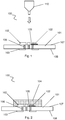
- the coating of the electrical component can take place, for example, with the help of aerosol deposition.
- the layer can also be applied, for example, with the help of CVD, for example according to the Gorham process.
- CVD also referred to as chemical vapor deposition
- a solid component is deposited as layer on the surface of a substrate due to a chemical reason from the vapor phase.
- Volatile compounds of the layer components thereby deposit a solid layer, often at an elevated temperature of the substrate of component.
- the CVD process is characterized by at least one chemical reaction on the surface of the substrate or component. At least one gaseous starting compound and at least two reaction products - at least one of which in the solid phase - have to be involved in this reaction.
- CVD processes which provide for a deposition at low temperature of the surface to be coated, i.e. of the component or substrate, for example plasma enhanced chemical vapor deposition (PECVD) or HFCVD processes (hot filament CVD) are particularly preferred.
- PECVD plasma enhanced chemical vapor deposition
- HFCVD hot filament CVD
- the Gorham process for the deposition of parylene is an example for a particularly preferred CVD process.
- a group of coating materials is referred to as parylenes.
- hydrocarbon poly-p-xylelene also referred to as parylene N
- halogenated derivatives thereof can be used as well.
- the layer is applied as closed polymer film to the component and/or substrate in a vacuum by means of resublimation from the vapor phase.
- Parylene has the structure wherein R1, R2, R3, R4, and X are selected independently of one another from hydrogen or halogens. Parylene N, parylene C, parylene D, and parylene HT are preferred parylenes.
- the Gorham process is a frequently used process for producing parylene, and is described in GORHAM (1966), "A New, General Synthetic Process for the Preparation of Linear Poly-p-xylylenes", J. Polym. Sci. A. 4 (12): 3027 ; which is hereby incorporated by reference in its entirety.
- Aerosol deposition refers to a process, in the case of which a jet of a particle material is directed at a surface of a substrate, which is to be coated.
- the particles are accelerated to a speed of, for example, 100 m/s or more, for example 200 m/s to 600 m/s, preferably 300 m/s to 500 m/s with the help of a carrier gas.
- a carrier gas for example, air, nitrogen, oxygen, argon, or helium are suitable carrier gases.
- Any carrier gas can generally be used, which does not undergo an unwanted chemical reaction with the material of the particles or of the substrate.
- the particles have a diameter of, for example, 200 nm to 2 ⁇ m.
- a plastic deformation of the particles and/or of the substrate results due to the kinetic energy of the impact, and a closed, consolidated layer thereby forms on the component from the particle material.
- This process is referred to as "room temperature impact consolidation".
- the layers formed thereby often display a very good adhesion to the component.
- Very even closed layers are created, which, compared to thermal spraying or screen printing, have improved properties with respect to roughness and freedom from defects.
- the aerosol deposition can be performed at normal room temperature, for example 20°C, and at higher pressures, for example 1 mbar, and provides a much higher deposition rate or higher layer thicknesses, respectively.
- particle speed and particle size have to be selected appropriately in the individual case, in order to provide for a coating.
- these parameters can be gathered from the literature and/or can be determined with simple tests, as described in the above-mentioned citations and the sources cited therein.
- particle sizes of, for example, 10 to 100 nm can be used with a particle speed of from 300 to 500 m/s.
- Implantable, electrical sensors, stimulators, or parts thereof, for example electrical feedthroughs are examples for electrical medical implants.
- Electrical feedthroughs and further systems for electrical medical implants, in particular on the basis of cermets, are described, for example, in US2011034966A1 , US2011034965A1 , US2014008121 A1 , US2011186349A1 , DE102010006837A1 , DE102010006838A1 , US2013299233A1 , US2012197327A1 , WO2013075797A1 , US2017047138A1 , US2012193118A1 , US2012194981A1 , US2012193141A1 , US2015122875A1 , US2012193119A1 , US2012197368A1 , US2014368298A1 , US2012203294A1 , US2012200011A1 , US2012197326A1 , EP3160580A1 , WO2016131976
- the substrate can generally be any carrier material, which is suitable for the production of an electrical medical implant and for the reception of an electrical component.
- Biocompatible materials such as, for example, a ceramic material, in particular Al 2 O 3 , or biocompatible metals or alloys, such as, for example, titanium, are preferred substrates.
- the ceramic material can comprise, for example, aluminum oxide (Al 2 O 3 ), magnesium oxide (MgO), zirconium oxide (ZrO 2 ), aluminum nitrate (Al 2 TiO 5 ), and piezoceramics, or mixtures thereof.
- the substrate can also comprise a metal selected from titanium (Ti), tantalum (Ta), iridium (Ir), niobium (Nb), or platinum (Pt), or an alloy of at least one of these metals.
- An electrical component can be any electrical component, which can be used in an electrical medical implant.
- Examples for electrical components comprise integrated circuits, transistors, capacitors, coils, antennas, voltage transformers, electrical resistors, and similar components.
- the electrical component is a component selected from the group consisting of a data memory, a data processing unit, a power source, a recording device, and a transmitting means, or a combination of at least two of them.
- Any unit for storing data which the person of skill in the art considers to be suitable for storing medical data, preferably ECG data, in an implantable device, can be selected as data memory.
- a preferred data memory is a magnetic memory or a flash memory or both.
- a preferred power source is a battery or an accumulator or both.
- a preferred recording device is a device for recording medical data, preferably cardio data, more preferably ECG data.
- a particularly preferred recording device is a biomonitor.
- a preferred biomonitor comprises an element selected from the group consisting of an ECG device, a Holter monitor, an event recorder, and a loop recorder, or a combination of at least two of them.
- a preferred ECG device is a long-term ECG device, which preferably stores data accumulating over a time period of at least one hour.
- a preferred transmitting means is formed for a wireless, preferably telemetric, transmission of data, preferably ECG data.
- a preferred wireless transmission of data is a transmission by means of waves. Preferred waves are longitudinal waves or transversal waves or both.
- Preferred longitudinal waves are acoustic waves or sound waves or both.
- Preferred transversal waves are electromagnetic waves.
- Preferred electromagnetic waves are waves of the frequency of a mobile radio network or of Bluetooth or both.
- a preferred mobile radio network is a GSM network.
- the component is set up to emit an electrical signal to the human body.
- the component is set up to receive an electrical signal from the human body.
- the electrical signal is associated with a physiological function.
- the component is a functional part of a sensor or stimulator, as described herein.
- a contact element is an electrically conductive element, which is set up for electrically contacting an electrical component with an electrical conductor.
- the contact element can be made, for example, of a metal or a metal alloy. Examples of such a contact element are described in US2013020714A1 .
- the contact element can be, for example, a contact pad, as it is common in the semiconductor industry, for example a SMD contact pad.
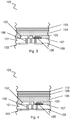
- the substrate comprises a first side, which carries the electrical component.
- the first side of the substrate may be or can be completely or partially coated, respectively, with the layer. For example, only the region of the substrate, which carries the electrical component, can be coated.
- the layer can be created, for example, by means of an aerosol deposition, as described herein.
- the surface of the component and/or substrate can thereby be coated by means of the raster process, also referred to as scanning, so that a location-selective coating of the component and/or substrate is possible.
- the coating of the component and/or substrate takes place in a location-selective manner. By scanning a region several times, higher layer thickness can be attained.
- the first side of the substrate, which carries the electrical component is completely or partially coated with a layer.
- the side of the substrate bearing the electrical component may be completely or partially scanned by means of a particle jet, as described above.
- mask processes can also be used in order to shield a portion of the substrate from the particle jet.
- particularly small structures and/or sharp dividing lines of the layer can be attained by means of a combination of scanning and masking.
- An only partial coating of a substrate surface can be helpful in order to keep free certain regions, for example portions of components, for the electrical contacting.
- the second side of the substrate can likewise carry electrical components, or can comprise, for example, only contact elements.
- an electrical lead connects the conduit element to the contact element.
- the electrical lead can be arranged on the second side of the substrate. It can be advantageous thereby to completely or partially coat, for example, the leads of the contact elements and/or the contact elements themselves with a layer, as described herein.
- the contact element is accessible for a direct electrical contacting after the coating of the component and/or of the substrate.
- the layer is preferably an essentially closed layer of an electrically insulating material.
- the layer is preferably essentially free from pores, holes (in particular so-called pinhole defects) and/or tears.
- the layer is set up to insulate the component to the outside.
- the layer protects the component against contact with air and/or human tissue.
- the layer can also protect the component against contact with an electrically conductive medium, for example a metal or a saline solution. The layer can thus protect the component against external influences, and can ensure an interruption-free function and long service life of the component.
- the layer can, for example, be partially or completely formed from an inorganic material.
- the layer is partially or completely formed from a ceramic material.
- the ceramic material can comprise, for example, aluminum oxide (Al 2 O 3 ), magnesium oxide (MgO), zirconium oxide (ZrO 2 ), aluminum nitrate (Al 2 TiO 5 ), and piezoceramics, or mixtures thereof.
- the layer can also comprise a polymer.
- the layer is formed from parylene.
- the polymer can also be applied together with an inorganic material, for example Al 2 O 3 , or can be applied in a separate process step.
- the polymer can be applied, for example, by means of aerosol deposition or CVD, as described herein. Parylene, polyimide, or Teflon, for example, are suitable polymers.
- the polymer is preferably a biocompatible polymer.
- the processes described herein can facilitate the coating of temperature-sensitive components.
- the processes can preferably be performed at low temperature.
- the coating of the component and/or substrate takes place, for example, below a temperature of 400°C, 300°C, 200°C, or below 100°C, more preferably below a temperature of 50°C, the coating of the component and/or substrate even more preferably takes place at approximately 25°C.
- the mentioned temperatures refer to the temperature of the component and/or substrate, whereby it is generally assumed that the component and/or substrate has the same or essentially the same temperature as the surrounding gas atmosphere.
- the processes can also be performed at higher pressures than other coating processes in the prior art.
- a high vacuum is thus not required in order to perform the coating.
- the coating of the component and/or substrate can take place, for example, in an atmosphere with a pressure of at least 0.1 Pa, 1 Pa, 5 Pa, or 10 Pa.
- the mentioned pressure refers to the pressure within the chamber, in which the coating of the substrate takes place.
- the pressure is thereby optionally determined outside of the particle jet, with the largest possible distance from the particle jet.
- a layer with a thickness of at least 100 nm, 500 nm, 1 ⁇ m, preferably at least 2, 3, 4, 5, 6, 7, 8, 9, or 10 ⁇ m, or more than 20 ⁇ m can be applied.
- the thickness of the layer is approximately 1 ⁇ m to 10 ⁇ m.
- the provision of the electrical feedthrough comprises a HTCC (high temperature cofired ceramics) or LTCC (low temperature cofired ceramics) process.
- HTCC and LTCC processes are described in EP3351290B1 , WO2011065989A1 , and Barlow/Elshabini: Ceramic Interconnect Technology Handbook, CRC Press, 2007 ; which are hereby incorporated by reference in their entirety.
- the provision of the electrical feedthrough comprises a lamination of several ceramic green body films.
- the green body films can include punched structures for receiving a metalliferous paste. By means of joint sintering with the green body films, conduit elements can be produced from the metalliferous paste.
- the conduit element can comprise a cermet.
- the substrate can comprise, for example, a ceramic material, for example Al 2 O 3
- the conduit element can comprise a cermet, wherein the cermet can comprise, for example, Al 2 O 3 .
- a composite material of a ceramic and a metal is referred to as "cermet".
- cermet A composite material of a ceramic and a metal
- a mixture of at least one ceramic powder and at least one metallic powder can be used to produce a cermet.
- At least one binding agent and optionally at least one solvent can be added to this mixture, in order to obtain a malleable green body. Afterwards, the binding agent and optionally the solvent are completely removed thermally and/or by means of evaporation during the so-called debinding. All substances, which are mentioned as ceramic materials herein, are generally suitable substances for the ceramic contained in the cermet.
- the cermet can be electrically conductive.
- An electrically conductive connection generally sets in in the cermet when the metal content lies above the so-called percolation threshold, at which the metal particles in the sintered cermet are connected to one another at least pointwise, so that an electrical conduction is made possible.
- the metal content can for this purpose be, for example, at least 25% by volume, depending on the material selection.
- the cermet can comprise a precious metal.
- the precious metal is preferably selected from the group consisting of platinum, silver, gold, tantalum, molybdenum, and titanium.
- an electrical feedthrough can be produced by means of the processes described herein, which comprises a conduit element, which has a cermet.
- a feedthrough can be produced as follows: At first, a green body film can be provided and can be provided with holes, for example by means of punching. The holes can be filled with a suitable cermet paste. At this stage of the production, the cermet paste can comprise at least a mixture of metal powder, ceramic powder, and an organic vehicle. Several of the green body films filled in this way can subsequently be laminated, so that the cermet-filled holes are arranged one on top of the other. They can subsequently form the conduit element.
- So many filled green body films can be laminated that the desired thickness of the electrical feedthrough or length of the conduit element, respectively, is reached.
- the organic vehicle can be removed at first, the cermet and the ceramic base body can be co-sintered during the subsequent transition to higher temperature.
- a hermetically tight substance-to-substance bond between the ceramic component of the cermet and the surrounding ceramic of the base body can be created thereby.
- the coating takes place with the help of particles with an average particle size of from 10 to 100 nm, 20 to 90 nm, 30 to 80 nm, or 40 to 70 nm.
- a further coating can take place after the coating of the component and/or substrate with the help of aerosol deposition, for example with a metal or a ceramic material.
- the ceramic material can preferably be Al 2 O 3 .
- a second layer of metal can be applied, for example, to the layer applied by means of the aerosol deposition method with the help of PVD, or a second layer of a ceramic material can be applied to the layer with the help of sputtering or evaporation.
- Aluminum is a preferred metal.
- the layer can also comprise a metal selected from titanium (Ti), tantalum (Ta), iridium (Ir), niobium (Nb), or platinum (Pt), or an alloy with at least one of these metals.
- a layer can be created, for example, directly on the layer, which is applied by means of aerosol deposition.
- the component is covered in this case with two different layers by means of the process by means of an aerosol deposition and a further coating process. It is also possible to apply two different layers one on top of the other to the component with the help of aerosol deposition.
- the layer can comprise, for example, Al 2 O 3
- the second layer can comprise aluminum; or the layer can comprise parylene and the second layer can comprise aluminum.
- the component can be coated, for example, with Al 2 O 3 by means of aerosol deposition, and an aluminum layer can be applied to the Al 2 O 3 layer with help of a suitable process, for example PVD.
- a layer of parylene is at first applied to the component, and a second layer of parylene is then applied to the first parylene layer.
- an Al 2 O 3 layer is at first applied to the component, preferably by means of an aerosol deposition, and a parylene layer is then applied.
- a parylene layer is at first applied to the component, and then a second layer of Al 2 O 3 is applied, preferably by means of an aerosol deposition.
- a parylene layer is at first applied to the component, then a second layer of Al 2 O 3 layer is applied, and a third layer of parylene is applied thereon, wherein the Al 2 O 3 layer is preferably applied by means of an aerosol deposition.
- a further aspect of the invention relates to an electrical medical implant, which can be produced or which is produced according to a process described herein.
- the layer produced according to a process described herein can have a helium leak rate of at least 1x10 -9 mbar*L/s.
- the electrically medical implant is hermetically tight.
- the term "hermetically tight" clarifies that moisture and/or gases cannot permeate or can only minimally permeate the hermetically tight element in the case of a proper use within the usual time periods (for example 5-10 years).
- a physical variable which can describe, for example, a permeation of gases and/or moisture through a device, e.g.
- leak rate which can be determined, for example, by means of leak tests.
- Corresponding leak tests can be performed, for example, with helium leak testers and are specified in the standard Mil-STD-883G Method 1014.
- the maximally permissible helium leak rate is thereby specified as a function of the internal volume of the device to be tested. According to the methods specified in MIL-STD-883G, Method 1014, in paragraph 3.1, and in consideration of the volumes occurring when using the present invention and cavities of the devices to be tested, these maximally permissible helium leak rates can be, for example, between 1 x 10 -8 atm ⁇ cm 3 /sec and 1 x 10 -7 atm ⁇ cm 3 /sec.
- the term "hermetically tight" can in particular mean that the workpiece to be tested, in particular the layer, has a helium leak rate of less than 1 x 10 -7 atm ⁇ cm 3 /sec.
- the helium leak rate can be less than 10 -8 , 10 -9 , 10 -10 , or less than 10 -11 mbar/L ⁇ s.
- the mentioned helium leak rate can also be converted into the equivalent standard air leak rate. The definition for the equivalent standard air leak rate) and the conversion are specified in the standard ISO 3530.
- the electrical medical implant can be, for example, a sensor or stimulator, or an electrical feedthrough for a sensor or stimulator.
- the electrical medical implant can be a pulse generator, pacemaker, cardiac resynchronization device, sensor, or stimulator.
- Such devices can be used, for example, in medical applications, such as neuromodulation, cardiac stimulation, deep brain stimulation, spinal cord stimulation, or gastric stimulation.
- a stimulator is an active implantable medical device, which can achieve a physiological effect by emitting an electrical signal to the body of a living being.
- a neurostimulator can affect, for example, an electrical signal in the nerve cell (e.g. an action potential) by emitting an electrical signal to a nerve cell.
- Pacemakers and cardioverter defibrillators are further examples for stimulators.
- a sensor is an implantable medical device, which can detect a physiological effect by receiving an electrical signal from the body of a living being.
- a cochlea implant or a retina implant is an example for a sensor.
- a further aspect of the invention relates to the use of a process described herein for producing an electrical medical implant.
- the implant can be, for example, a sensor or stimulator, as described above.
- a further aspect of the invention relates to an electrical feedthrough for an electrical medical implant, which comprises a component, which is covered with a layer.
- a further aspect of the invention relates to an electrical medical implant, comprising an electrical feedthrough, which comprises a substrate, an electrical component, and a contact element, wherein the electrical component is arranged on a first side of the substrate and is coated with a layer.
- the layer comprises parylene or a ceramic material, preferably Al 2 O 3 , or consists thereof.
- the component is covered by several layers.
- the component is covered by a parylene layer and an Al 2 O 3 layer.
- the component is covered by two parylene layers.
- the component is covered by two parylene layers and an Al 2 O 3 layer located therebetween.
- the electrical component is connected to the substrate directly or only via a printed circuit board.
- the first side of the substrate can be completely or partially coated with the layer, as described above in connection with the process according to the invention.
- the implant can comprise a conduit element, which is arranged essentially completely within the substrate and which extends from the first side of the substrate to an opposite second side of the substrate.
- the electrical component can thereby be connected to the conduit element directly or only via a printed circuit board.
- the electrical component can also be connected to the substrate directly or only via a printed circuit board. This means in particular that the electrical component is arranged directly on the substrate or at least at a very small distance from the substrate.
- the component can, for example, be arranged directly on the substrate in the so-called SMD design (surface mounted device).
- the component can also be arranged directly on a printed circuit board, which, in turn, is arranged directly on the substrate.
- a solder paste or a comparable connecting materials is neglected in the definition according to the invention for fulfilling the feature "arranged directly on", i.e. a component or a printed circuit board herein also applies as being arranged directly on the substrate when a thin layer of solder or a comparable material, which does not have a significant impact on the structural design of the implant, is located therebetween.
- a component which is connected to the substrate via a wire or a cable with a length of, for example, more than 1 mm, and which is arranged at a corresponding spatial distance from the substrate, is not arranged directly on the substrate.
- the above applies analogously for the direct connection of the component to the conduit element.
- the conduit element is preferably arranged essentially completely within the substrate, i.e. it extends essentially exclusively in the region between the first side and the second side of the substrate, and serves, for example, for establishing an electrical contact between the contact element on the second side to the electrical component on the first side of the substrate.
- the implant can be implanted in the human body without housing.
- the implant does not include a housing element, and can be implanted in the body with direct tissue contact without a housing, without impacting the function of the implant.
- "Implanted in the body” can thereby comprise the attachment of the implant to the skin, or the surgical insertion of the implant in the human body.
- "implanted in the body” comprises the direct contact of the implant with tissue fluid in the human body.
- the metal layer described herein, which, as described herein, can be comprised as part of the layer according to the invention, is not understood as housing element herein.
- a ceramic layer can be applied directly to the component, and a metal layer can be applied directly to the ceramic layer.
- Such a composite layer which can have, for example, a total thickness of less than 100 ⁇ m, is not understood as “housing element” or “housing” herein.
- the layer of the implant has a helium leak rate of less than 1x10 -9 mbar*L/s. In one embodiment, the layer is hermetically tight, as described herein.
- the layer has a thickness of approximately 1 ⁇ m to 50 ⁇ m. In one embodiment, the thickness of the layer is approximately 1 ⁇ m to 10 ⁇ m.
- the layer can also have a thickness of more than 10 ⁇ m, for example approximately 11, 12, 15, or 20 ⁇ m, 30 ⁇ m, 40 ⁇ m, 50 ⁇ m, or more than 50 ⁇ m.
- the conduit element comprises a cermet, as described above in connection with the process.
- the cermet can comprise, for example, Al 2 O 3 and platinum, as described above.
- the contact element is accessible for a direct electrical contacting after the coating.
- This can be attained, for example, in that the substrate is coated such that the contact element is not completely covered by the layer.
- This can be attained, for example, by means of location-selective coating with the help of a raster process or mask process.
- the substrate is coated on the first side of the substrate, which carries the component, and the second side of the substrate, which carries the contact element, is not or only partially coated, so that the contact element is not completely covered by the layer.
- the layer can comprise a polymer, for example a parylene, or a ceramic material, as described herein, or can consist thereof.
- the layer can comprise, for example, Al 2 O 3 .
- the layer preferably has a thickness of at least 1, 2, 3, 4, 5, 6, 7, 8, 9, or 10 ⁇ m.
- the component can comprise a temperature-sensitive component, for example a component, which is specified for a use and/or processing at temperatures of below 300, 250, 200, 150, or below 100°C.
- Al 2 O 3 green films were sintered at a sintering temperature of 1450°C (samples identified as "low” in Tab. 1) or 1550°C (all other samples) for 5 hours in air, in order to produce plates of porous Al 2 O 3 ceramic. These plates were coated with Al 2 O 3 particles with the help of aerosol deposition and/or were coated with parylene according to the Gorham process. Before and after the coating, the plates were examined in a helium leak test. All samples were measured in 2 different orientations. The results of these measurements are displayed in Tab. 1. The first value of a sample in each case specifies the helium leak rate in orientation 1, while the respective second value of a sample specifies the helium leak rate in orientation 2.
Landscapes
- Engineering & Computer Science (AREA)
- Health & Medical Sciences (AREA)
- Life Sciences & Earth Sciences (AREA)
- Microelectronics & Electronic Packaging (AREA)
- Manufacturing & Machinery (AREA)
- Public Health (AREA)
- Biomedical Technology (AREA)
- Veterinary Medicine (AREA)
- Animal Behavior & Ethology (AREA)
- General Health & Medical Sciences (AREA)
- Nuclear Medicine, Radiotherapy & Molecular Imaging (AREA)
- Radiology & Medical Imaging (AREA)
- Physics & Mathematics (AREA)
- Biophysics (AREA)
- Pathology (AREA)
- Heart & Thoracic Surgery (AREA)
- Medical Informatics (AREA)
- Molecular Biology (AREA)
- Surgery (AREA)
- Prostheses (AREA)
- Materials For Medical Uses (AREA)
Abstract
Description
- The present invention relates to the field of medical technology, in particular active implants, for example electrical feedthroughs for sensors and stimulators.
- Active medical implants, such as, for example, pacemakers or cochlea implants, are often encapsulated in a housing made of metal. To produce such a housing, for example two housing parts made of titanium can be welded together. Such a housing part can comprise an electrical feedthrough, which provides for an electrical connection through the housing. Inside and/or outside of a housing, active medical implants usually comprise different electrical components, which have to be electrically connected to one another. In many cases, the electrical components have to be protected against contact with tissue and tissue fluid, in order to prevent damage to the components or unwanted impacts on the tissue. In particular, no tissue fluid must permeate into the housing. High demands are thus made on the tightness of electrical feedthroughs for active medical implants. Electrical feedthroughs are often installed in a housing with the help of a welding flange. The welding flange can be soldered to the housing, and the electrical feedthrough can be welded to the flange, for example by means of laser welding.
- The object of the present invention is to solve one or several of the above-described and additional problems of the prior art. For example, the invention provides for an improved production process for electrical medical implants, which is simpler and more cost-efficient, for example. The present invention furthermore provides electrical medical implants comprising an improved tightness and smaller weight.
These objects are solved by means of the processes and devices described herein, in particular those, which are described in the patent claims.
Preferred embodiments of the invention will be described below. - 1. A process for producing an electrical medical implant, comprising the following steps:
- a. providing an electrical feedthrough, which comprises a substrate, an electrical component, and a contact element,
- b. coating the electrical component with a layer.
- 2. The process according to embodiment 1, wherein the coating of the electrical component takes place with the help of aerosol deposition or CVD, preferably according to the Gorham process.
- 3. The process according to any one of the preceding embodiments, wherein the substrate comprises a first side, which carries the electrical component, and the first side of the substrate is completely or partially coated with a layer.
- 4. The process according to any one of the preceding embodiments, wherein the layer is made of parylene or a ceramic material.
- 5. The process according to embodiment 4, wherein the ceramic material comprises Al2O3 or consists thereof.
- 6. The process according to any one of the preceding embodiments, wherein after the coating, the contact element is accessible for a direct electrical contacting.
- 7. The process according to any one of the preceding embodiments, wherein the coating takes place below a temperature of 100 °C, preferably below a temperature of 50 °C, more preferably at approximately 25 °C.
- 8. The process according to any one of the preceding embodiments, wherein the coating takes place in an atmosphere with a pressure of at least 10 Pa.
- 9. The process according to any one of the preceding embodiments, wherein the layer has a thickness of approximately 1 µm to 10 µm, preferably 1 µm to 50 µm.
- 10. The process according to any one of the preceding embodiments, wherein the provision of the electrical feedthrough comprises a HTCC or LTCC process.
- 11. The process according to any one of the preceding embodiments, wherein the substate comprises a ceramic material.
- 12. The process according to any one of the preceding embodiments, wherein the conduit element comprises a cermet.
- 13. The process according to any one of the preceding embodiments, wherein the coating takes place with the help of particles with an average particle size of from 10 to 100 nm.
- 14. The process according to any one of the preceding embodiments, wherein a further coating with metal or ceramic takes place after the coating of the component and/or substrate with the help of aerosol deposition.
- 15. The process according to embodiment 13, wherein the further coating takes place by means of PVD, vapor deposition, or sputtering.
- 16. The process according to embodiment 13 or 14, wherein the further coating creates a second layer directly on the previously applied layer.
- 17. The process according to any one of the preceding embodiments 14 to 16, wherein several layers of parylene, or a parylene layer and an Al2O3 layer are applied to the component, wherein the Al2O3 layer is preferably applied by means of an aerosol deposition.
- 18. An electrical medical implant, produced according to a process according to any one of the preceding embodiments.
- 19. The electrical medical implant according to embodiment 18, wherein the layer has a helium leak rate of less than 1x10⁻⁹ mbar*L/s.
- 20. Use of a process according to any one of embodiments 1 to 18 for producing an electrical medical implant.
- 21. An electrical medical implant, comprising an electrical feedthrough, which comprises a substrate, an electrical component, and a contact element, wherein the electrical component is arranged on a first side of the substrate and is coated with a layer.
- 22. The implant according to embodiment 21, wherein the layer comprises parylene or a ceramic material, preferably Al2O3, or consists thereof.
- 23. The implant according to embodiment 21 or 22, wherein the electrical component is connected to the substrate directly or only via a printed circuit board.
- 24. The implant according to any one of embodiments 21 to 23, wherein the first side of the substrate is completely or partially coated with the layer.
- 25. The implant according to any one of embodiments 21 to 24, comprising a conduit element, which is arranged essentially completely within the substrate and extends from the first side of the substrate to an opposite second side of the substrate, wherein the electrical component is preferably connected to the conduit element directly or only via a printed circuit board.
- 26. The implant according to any one of embodiments 21 to 25, which can be implanted in the human body without housing.
- 27. The implant according to any one of embodiments 21 to 26, wherein the layer has a helium leak rate of less than 1x10⁻⁹ mbar*L/s.
- 28. The implant according to any one of embodiments 21 to 27, wherein the layer has a thickness of approximately 1 µm to 50 µm, preferably 1 µm to 10 µm.
- 29. The implant according to any one of embodiments 21 to 28, wherein the conduit element comprises a cermet.
- 30. The implant according to any one of embodiments 21 to 29, wherein, after the coating, the contact element is accessible for a direct electrical contacting.
- 31. The implant according to any one of embodiments 21 to 30, wherein the contact element is not completely covered by the layer.
- 32. The implant according to any one of embodiments 21 to 31, wherein several layers of parylene, or a parylene layer and an Al2O3 layer are applied to the component, wherein the Al2O3 layer is preferably applied by means of an aerosol deposition.
- In addition to the embodiments described herein, the elements of which "have" or "comprise" a certain feature (e.g. a material), a further embodiment is generally always considered, in which the respective element consists solely of the feature, i.e. does not comprise any further components. The word "comprise" or "comprising" is used synonymously with the word "have" or "having" herein.
When an element is identified in the singular form in an embodiment, an embodiment is likewise contemplated in which several of these elements are present. The use of a term for an element in the plural form generally also comprises an embodiment, in which only an individual such element is present.
Unless otherwise specified or excluded unambiguously from the context, it is generally possible and is hereby unambiguously considered that features of different embodiments can also be present in the other embodiments described herein. It is likewise generally considered that all features, which are described herein in connection with a process, can also be used for the products and devices described herein, and vice versa. All of these considered combinations are not listed explicitly in all cases only in the interest of a more concise description. Technical solutions, which are obviously equivalent to the features described herein, are to generally be comprised by the scope of the invention. - A first aspect of the invention relates to a process for producing an electrical medical implant, which comprises the following steps:
- a. providing an electrical feedthrough, which comprises a substrate, an electrical component, and a contact element,
- b. coating the electrical component with a layer.
- The layer is preferably created from a vapor phase. The coating of the electrical component can take place, for example, with the help of aerosol deposition. In the alternative, the layer can also be applied, for example, with the help of CVD, for example according to the Gorham process.
- In the case of CVD, also referred to as chemical vapor deposition, a solid component is deposited as layer on the surface of a substrate due to a chemical reason from the vapor phase.
Volatile compounds of the layer components thereby deposit a solid layer, often at an elevated temperature of the substrate of component. The CVD process is characterized by at least one chemical reaction on the surface of the substrate or component. At least one gaseous starting compound and at least two reaction products - at least one of which in the solid phase - have to be involved in this reaction. - CVD processes, which provide for a deposition at low temperature of the surface to be coated, i.e. of the component or substrate, for example plasma enhanced chemical vapor deposition (PECVD) or HFCVD processes (hot filament CVD) are particularly preferred.
The Gorham process for the deposition of parylene is an example for a particularly preferred CVD process. A group of coating materials is referred to as parylenes. In addition to the hydrocarbon poly-p-xylelene (also referred to as parylene N), halogenated derivatives thereof can be used as well. The layer is applied as closed polymer film to the component and/or substrate in a vacuum by means of resublimation from the vapor phase.
Parylene has the structure
- Aerosol deposition refers to a process, in the case of which a jet of a particle material is directed at a surface of a substrate, which is to be coated. For this purpose, the particles are accelerated to a speed of, for example, 100 m/s or more, for example 200 m/s to 600 m/s, preferably 300 m/s to 500 m/s with the help of a carrier gas. For example, air, nitrogen, oxygen, argon, or helium are suitable carrier gases. Any carrier gas can generally be used, which does not undergo an unwanted chemical reaction with the material of the particles or of the substrate. At first, the particles have a diameter of, for example, 200 nm to 2 µm. A plastic deformation of the particles and/or of the substrate results due to the kinetic energy of the impact, and a closed, consolidated layer thereby forms on the component from the particle material. This process is referred to as "room temperature impact consolidation". The layers formed thereby often display a very good adhesion to the component. Very even closed layers are created, which, compared to thermal spraying or screen printing, have improved properties with respect to roughness and freedom from defects. In contrast to comparable processes of the chemical vapor deposition, the aerosol deposition can be performed at normal room temperature, for example 20°C, and at higher pressures, for example 1 mbar, and provides a much higher deposition rate or higher layer thicknesses, respectively. Layer thicknesses of several micrometers can be attained within a few minutes, for example, with the help of aerosol deposition. This is particularly advantageous in the case of temperature-sensitive electrical components. The process of the aerosol deposition is described in further details, for example in J. AKEDO et al., Room Temperature Impact Consolidation (RTIC) of Fine Ceramic Powder by Aerosol Deposition Process and Applications to Microdevices, J. Therm. SprayTech., 17, 181-198 (2008); and D. HANFT et al : An Overview of the Aerosol Deposition Process: Process Fundamentals and New Trends in Materials Applications, Journal of Ceramic Science and Technology, 6, 147-182 (2015), which are hereby incorporated completely by reference.
Depending on the used material of the particles and the surface to be coated, i.e. of the component and/or substrate, particle speed and particle size have to be selected appropriately in the individual case, in order to provide for a coating. For some materials, these parameters can be gathered from the literature and/or can be determined with simple tests, as described in the above-mentioned citations and the sources cited therein. In many cases, particle sizes of, for example, 10 to 100 nm can be used with a particle speed of from 300 to 500 m/s. - Implantable, electrical sensors, stimulators, or parts thereof, for example electrical feedthroughs, are examples for electrical medical implants. Electrical feedthroughs and further systems for electrical medical implants, in particular on the basis of cermets, are described, for example, in
US2011034966A1 ,US2011034965A1 ,US2014008121 A1 ,US2011186349A1 ,DE102010006837A1 ,DE102010006838A1 ,US2013299233A1 ,US2012197327A1 ,WO2013075797A1 ,US2017047138A1 ,US2012193118A1 ,US2012194981A1 ,US2012193141A1 ,US2015122875A1 ,US2012193119A1 ,US2012197368A1 ,US2014368298A1 ,US2012203294A1 ,US2012200011A1 ,US2012197326A1 ,EP3160580A1 ,WO2016131976A1 ,EP3284515A1 ,US2018050211 A1 ,US2018050212A1 ,US2018213665A andEP3398650A1 , which are hereby incorporated completely by reference. - The substrate can generally be any carrier material, which is suitable for the production of an electrical medical implant and for the reception of an electrical component. Biocompatible materials, such as, for example, a ceramic material, in particular Al2O3, or biocompatible metals or alloys, such as, for example, titanium, are preferred substrates. The ceramic material can comprise, for example, aluminum oxide (Al2O3), magnesium oxide (MgO), zirconium oxide (ZrO2), aluminum nitrate (Al2TiO5), and piezoceramics, or mixtures thereof. The substrate can also comprise a metal selected from titanium (Ti), tantalum (Ta), iridium (Ir), niobium (Nb), or platinum (Pt), or an alloy of at least one of these metals.
- An electrical component can be any electrical component, which can be used in an electrical medical implant. Examples for electrical components comprise integrated circuits, transistors, capacitors, coils, antennas, voltage transformers, electrical resistors, and similar components. In an embodiment according to the invention, the electrical component is a component selected from the group consisting of a data memory, a data processing unit, a power source, a recording device, and a transmitting means, or a combination of at least two of them. Any unit for storing data, which the person of skill in the art considers to be suitable for storing medical data, preferably ECG data, in an implantable device, can be selected as data memory. A preferred data memory is a magnetic memory or a flash memory or both. A preferred power source is a battery or an accumulator or both. A preferred recording device is a device for recording medical data, preferably cardio data, more preferably ECG data. A particularly preferred recording device is a biomonitor. A preferred biomonitor comprises an element selected from the group consisting of an ECG device, a Holter monitor, an event recorder, and a loop recorder, or a combination of at least two of them. A preferred ECG device is a long-term ECG device, which preferably stores data accumulating over a time period of at least one hour. A preferred transmitting means is formed for a wireless, preferably telemetric, transmission of data, preferably ECG data. A preferred wireless transmission of data is a transmission by means of waves. Preferred waves are longitudinal waves or transversal waves or both. Preferred longitudinal waves are acoustic waves or sound waves or both. Preferred transversal waves are electromagnetic waves. Preferred electromagnetic waves are waves of the frequency of a mobile radio network or of Bluetooth or both. A preferred mobile radio network is a GSM network.
In one embodiment, the component is set up to emit an electrical signal to the human body. In one embodiment, the component is set up to receive an electrical signal from the human body. In an embodiment system, the electrical signal is associated with a physiological function. In one embodiment, the component is a functional part of a sensor or stimulator, as described herein. - A contact element is an electrically conductive element, which is set up for electrically contacting an electrical component with an electrical conductor. The contact element can be made, for example, of a metal or a metal alloy. Examples of such a contact element are described in
US2013020714A1 . The contact element can be, for example, a contact pad, as it is common in the semiconductor industry, for example a SMD contact pad. - In one embodiment, the substrate comprises a first side, which carries the electrical component. The first side of the substrate may be or can be completely or partially coated, respectively, with the layer. For example, only the region of the substrate, which carries the electrical component, can be coated.
- The layer can be created, for example, by means of an aerosol deposition, as described herein. By controlling the particle jet, the surface of the component and/or substrate can thereby be coated by means of the raster process, also referred to as scanning, so that a location-selective coating of the component and/or substrate is possible. In one embodiment, the coating of the component and/or substrate takes place in a location-selective manner. By scanning a region several times, higher layer thickness can be attained.
- In one embodiment, the first side of the substrate, which carries the electrical component, is completely or partially coated with a layer. For example, the side of the substrate bearing the electrical component may be completely or partially scanned by means of a particle jet, as described above. In the alternative or in addition, mask processes can also be used in order to shield a portion of the substrate from the particle jet. For example, particularly small structures and/or sharp dividing lines of the layer can be attained by means of a combination of scanning and masking. An only partial coating of a substrate surface can be helpful in order to keep free certain regions, for example portions of components, for the electrical contacting. The above applies analogously for the second side of the substrate opposite to the first side, whereby the second side of the substrate can likewise carry electrical components, or can comprise, for example, only contact elements. In some embodiments, an electrical lead connects the conduit element to the contact element. The electrical lead can be arranged on the second side of the substrate. It can be advantageous thereby to completely or partially coat, for example, the leads of the contact elements and/or the contact elements themselves with a layer, as described herein. In one embodiment, the contact element is accessible for a direct electrical contacting after the coating of the component and/or of the substrate.
- The layer is preferably an essentially closed layer of an electrically insulating material. The layer is preferably essentially free from pores, holes (in particular so-called pinhole defects) and/or tears. In one embodiment, the layer is set up to insulate the component to the outside. For example, the layer protects the component against contact with air and/or human tissue. The layer can also protect the component against contact with an electrically conductive medium, for example a metal or a saline solution. The layer can thus protect the component against external influences, and can ensure an interruption-free function and long service life of the component.
- The layer can, for example, be partially or completely formed from an inorganic material. In one embodiment, the layer is partially or completely formed from a ceramic material. The ceramic material can comprise, for example, aluminum oxide (Al2O3), magnesium oxide (MgO), zirconium oxide (ZrO2), aluminum nitrate (Al2TiO5), and piezoceramics, or mixtures thereof.
- The layer can also comprise a polymer. In one embodiment, the layer is formed from parylene. The polymer can also be applied together with an inorganic material, for example Al2O3, or can be applied in a separate process step. The polymer can be applied, for example, by means of aerosol deposition or CVD, as described herein. Parylene, polyimide, or Teflon, for example, are suitable polymers. The polymer is preferably a biocompatible polymer.
- The processes described herein facilitate the production of electrical medical implants, which do not require a housing.
- The processes described herein can facilitate the coating of temperature-sensitive components. The processes can preferably be performed at low temperature. In one embodiment, the coating of the component and/or substrate takes place, for example, below a temperature of 400°C, 300°C, 200°C, or below 100°C, more preferably below a temperature of 50°C, the coating of the component and/or substrate even more preferably takes place at approximately 25°C. The mentioned temperatures refer to the temperature of the component and/or substrate, whereby it is generally assumed that the component and/or substrate has the same or essentially the same temperature as the surrounding gas atmosphere.
- The processes can also be performed at higher pressures than other coating processes in the prior art. A high vacuum is thus not required in order to perform the coating. The coating of the component and/or substrate can take place, for example, in an atmosphere with a pressure of at least 0.1 Pa, 1 Pa, 5 Pa, or 10 Pa. The mentioned pressure refers to the pressure within the chamber, in which the coating of the substrate takes place. The pressure is thereby optionally determined outside of the particle jet, with the largest possible distance from the particle jet.
- The processes described herein provide for higher layer thicknesses than other coating processes, in particular when coating with a layer of a ceramic material. For example, a layer with a thickness of at least 100 nm, 500 nm, 1 µm, preferably at least 2, 3, 4, 5, 6, 7, 8, 9, or 10 µm, or more than 20 µm, can be applied. In one embodiment, the thickness of the layer is approximately 1 µm to 10 µm.
- In one embodiment, the provision of the electrical feedthrough comprises a HTCC (high temperature cofired ceramics) or LTCC (low temperature cofired ceramics) process. Examples for HTCC and LTCC processes are described in
EP3351290B1 ,WO2011065989A1 , and Barlow/Elshabini: Ceramic Interconnect Technology Handbook, CRC Press, 2007; which are hereby incorporated by reference in their entirety. In one embodiment, the provision of the electrical feedthrough comprises a lamination of several ceramic green body films. The green body films can include punched structures for receiving a metalliferous paste. By means of joint sintering with the green body films, conduit elements can be produced from the metalliferous paste. - In one embodiment, the conduit element can comprise a cermet. The substrate can comprise, for example, a ceramic material, for example Al2O3, and the conduit element can comprise a cermet, wherein the cermet can comprise, for example, Al2O3. A composite material of a ceramic and a metal is referred to as "cermet". For example, a mixture of at least one ceramic powder and at least one metallic powder can be used to produce a cermet. At least one binding agent and optionally at least one solvent can be added to this mixture, in order to obtain a malleable green body. Afterwards, the binding agent and optionally the solvent are completely removed thermally and/or by means of evaporation during the so-called debinding. All substances, which are mentioned as ceramic materials herein, are generally suitable substances for the ceramic contained in the cermet.
- The cermet can be electrically conductive. An electrically conductive connection generally sets in in the cermet when the metal content lies above the so-called percolation threshold, at which the metal particles in the sintered cermet are connected to one another at least pointwise, so that an electrical conduction is made possible. According to experience, the metal content can for this purpose be, for example, at least 25% by volume, depending on the material selection.
- The cermet can comprise a precious metal. The precious metal is preferably selected from the group consisting of platinum, silver, gold, tantalum, molybdenum, and titanium.
- For example, an electrical feedthrough can be produced by means of the processes described herein, which comprises a conduit element, which has a cermet. For example, such a feedthrough can be produced as follows: At first, a green body film can be provided and can be provided with holes, for example by means of punching. The holes can be filled with a suitable cermet paste. At this stage of the production, the cermet paste can comprise at least a mixture of metal powder, ceramic powder, and an organic vehicle. Several of the green body films filled in this way can subsequently be laminated, so that the cermet-filled holes are arranged one on top of the other. They can subsequently form the conduit element. So many filled green body films can be laminated that the desired thickness of the electrical feedthrough or length of the conduit element, respectively, is reached. During the subsequent firing, the organic vehicle can be removed at first, the cermet and the ceramic base body can be co-sintered during the subsequent transition to higher temperature. In particular a hermetically tight substance-to-substance bond between the ceramic component of the cermet and the surrounding ceramic of the base body can be created thereby.
- In a further embodiment, the coating takes place with the help of particles with an average particle size of from 10 to 100 nm, 20 to 90 nm, 30 to 80 nm, or 40 to 70 nm.
- In some embodiments, a further coating can take place after the coating of the component and/or substrate with the help of aerosol deposition, for example with a metal or a ceramic material. The ceramic material can preferably be Al2O3. A second layer of metal can be applied, for example, to the layer applied by means of the aerosol deposition method with the help of PVD, or a second layer of a ceramic material can be applied to the layer with the help of sputtering or evaporation. Aluminum is a preferred metal. The layer can also comprise a metal selected from titanium (Ti), tantalum (Ta), iridium (Ir), niobium (Nb), or platinum (Pt), or an alloy with at least one of these metals. Due to the further coating, a layer can be created, for example, directly on the layer, which is applied by means of aerosol deposition. The component is covered in this case with two different layers by means of the process by means of an aerosol deposition and a further coating process. It is also possible to apply two different layers one on top of the other to the component with the help of aerosol deposition. The layer can comprise, for example, Al2O3, and the second layer can comprise aluminum; or the layer can comprise parylene and the second layer can comprise aluminum. At first, the component can be coated, for example, with
Al2O3 by means of aerosol deposition, and an aluminum layer can be applied to the Al2O3 layer with help of a suitable process, for example PVD. In one embodiment, several layers of parylene, or a parylene layer and an Al2O3 layer can be applied to the component, whereby the Al2O3 layer is preferably applied by means of an aerosol deposition.
In one embodiment, a layer of parylene is at first applied to the component, and a second layer of parylene is then applied to the first parylene layer. In one embodiment, an Al2O3 layer is at first applied to the component, preferably by means of an aerosol deposition, and a parylene layer is then applied. In one embodiment, a parylene layer is at first applied to the component, and then a second layer of Al2O3 is applied, preferably by means of an aerosol deposition. In one embodiment, a parylene layer is at first applied to the component, then a second layer of Al2O3 layer is applied, and a third layer of parylene is applied thereon, wherein the Al2O3 layer is preferably applied by means of an aerosol deposition. - A further aspect of the invention relates to an electrical medical implant, which can be produced or which is produced according to a process described herein. In the case of such an electrical medical implant, the layer produced according to a process described herein can have a helium leak rate of at least 1x10⁻⁹ mbar*L/s.
In one embodiment, the electrically medical implant is hermetically tight. The term "hermetically tight" clarifies that moisture and/or gases cannot permeate or can only minimally permeate the hermetically tight element in the case of a proper use within the usual time periods (for example 5-10 years). A physical variable, which can describe, for example, a permeation of gases and/or moisture through a device, e.g. through the electrical feedthrough, is the so-called leak rate, which can be determined, for example, by means of leak tests. Corresponding leak tests can be performed, for example, with helium leak testers and are specified in the standard Mil-STD-883G Method 1014. The maximally permissible helium leak rate is thereby specified as a function of the internal volume of the device to be tested. According to the methods specified in MIL-STD-883G, Method 1014, in paragraph 3.1, and in consideration of the volumes occurring when using the present invention and cavities of the devices to be tested, these maximally permissible helium leak rates can be, for example, between 1 x 10⁻⁸ atm·cm3/sec and 1 x 10⁻⁷ atm·cm3/sec. In the context of the invention, the term "hermetically tight" can in particular mean that the workpiece to be tested, in particular the layer, has a helium leak rate of less than 1 x 10⁻⁷ atm·cm3/sec. In an advantageous embodiment, the helium leak rate can be less than 10-8, 10-9, 10-10, or less than 10-11 mbar/L·s. For the purpose of the standardization, the mentioned helium leak rate can also be converted into the equivalent standard air leak rate. The definition for the equivalent standard air leak rate) and the conversion are specified in the standard ISO 3530. - The electrical medical implant can be, for example, a sensor or stimulator, or an electrical feedthrough for a sensor or stimulator.
The electrical medical implant can be a pulse generator, pacemaker, cardiac resynchronization device, sensor, or stimulator. Such devices can be used, for example, in medical applications, such as neuromodulation, cardiac stimulation, deep brain stimulation, spinal cord stimulation, or gastric stimulation. Here, a stimulator is an active implantable medical device, which can achieve a physiological effect by emitting an electrical signal to the body of a living being. A neurostimulator can affect, for example, an electrical signal in the nerve cell (e.g. an action potential) by emitting an electrical signal to a nerve cell. Pacemakers and cardioverter defibrillators are further examples for stimulators.
Here, a sensor is an implantable medical device, which can detect a physiological effect by receiving an electrical signal from the body of a living being. A cochlea implant or a retina implant is an example for a sensor. - A further aspect of the invention relates to the use of a process described herein for producing an electrical medical implant. The implant can be, for example, a sensor or stimulator, as described above.
- A further aspect of the invention relates to an electrical feedthrough for an electrical medical implant, which comprises a component, which is covered with a layer.
- A further aspect of the invention relates to an electrical medical implant, comprising an electrical feedthrough, which comprises a substrate, an electrical component, and a contact element, wherein the electrical component is arranged on a first side of the substrate and is coated with a layer.
- As already mentioned, all embodiments and features, which are described above in connection with the process according to the invention, are generally used for this aspect of the invention.
- In one embodiment, the layer comprises parylene or a ceramic material, preferably Al2O3, or consists thereof.
In one embodiment, the component is covered by several layers. In one embodiment, the component is covered by a parylene layer and an Al2O3 layer. In one embodiment, the component is covered by two parylene layers. In one embodiment, the component is covered by two parylene layers and an Al2O3 layer located therebetween. - In one embodiment, the electrical component is connected to the substrate directly or only via a printed circuit board.
- The first side of the substrate can be completely or partially coated with the layer, as described above in connection with the process according to the invention.
- The implant can comprise a conduit element, which is arranged essentially completely within the substrate and which extends from the first side of the substrate to an opposite second side of the substrate. The electrical component can thereby be connected to the conduit element directly or only via a printed circuit board. The electrical component can also be connected to the substrate directly or only via a printed circuit board. This means in particular that the electrical component is arranged directly on the substrate or at least at a very small distance from the substrate. The component can, for example, be arranged directly on the substrate in the so-called SMD design (surface mounted device). The component can also be arranged directly on a printed circuit board, which, in turn, is arranged directly on the substrate. A solder paste or a comparable connecting materials is neglected in the definition according to the invention for fulfilling the feature "arranged directly on", i.e. a component or a printed circuit board herein also applies as being arranged directly on the substrate when a thin layer of solder or a comparable material, which does not have a significant impact on the structural design of the implant, is located therebetween. In contrast, a component, which is connected to the substrate via a wire or a cable with a length of, for example, more than 1 mm, and which is arranged at a corresponding spatial distance from the substrate, is not arranged directly on the substrate. The above applies analogously for the direct connection of the component to the conduit element. The conduit element is preferably arranged essentially completely within the substrate, i.e. it extends essentially exclusively in the region between the first side and the second side of the substrate, and serves, for example, for establishing an electrical contact between the contact element on the second side to the electrical component on the first side of the substrate.
- In one embodiment, the implant can be implanted in the human body without housing. This means that the implant does not include a housing element, and can be implanted in the body with direct tissue contact without a housing, without impacting the function of the implant. "Implanted in the body" can thereby comprise the attachment of the implant to the skin, or the surgical insertion of the implant in the human body. In some embodiments, "implanted in the body" comprises the direct contact of the implant with tissue fluid in the human body. The metal layer described herein, which, as described herein, can be comprised as part of the layer according to the invention, is not understood as housing element herein. For example, a ceramic layer can be applied directly to the component, and a metal layer can be applied directly to the ceramic layer. Such a composite layer, which can have, for example, a total thickness of less than 100 µm, is not understood as "housing element" or "housing" herein.
- In one embodiment, the layer of the implant has a helium leak rate of less than 1x10⁻⁹ mbar*L/s. In one embodiment, the layer is hermetically tight, as described herein.
- In one embodiment, the layer has a thickness of approximately 1 µm to 50 µm. In one embodiment, the thickness of the layer is approximately 1 µm to 10 µm. The layer can also have a thickness of more than 10 µm, for example approximately 11, 12, 15, or 20 µm, 30 µm, 40 µm, 50 µm, or more than 50 µm.
- In one embodiment, the conduit element comprises a cermet, as described above in connection with the process. The cermet can comprise, for example, Al2O3 and platinum, as described above.
- In one embodiment, the contact element is accessible for a direct electrical contacting after the coating. This can be attained, for example, in that the substrate is coated such that the contact element is not completely covered by the layer. This can be attained, for example, by means of location-selective coating with the help of a raster process or mask process. In one embodiment, the substrate is coated on the first side of the substrate, which carries the component, and the second side of the substrate, which carries the contact element, is not or only partially coated, so that the contact element is not completely covered by the layer.
- The layer can comprise a polymer, for example a parylene, or a ceramic material, as described herein, or can consist thereof. The layer can comprise, for example, Al2O3. The layer preferably has a thickness of at least 1, 2, 3, 4, 5, 6, 7, 8, 9, or 10 µm. The component can comprise a temperature-sensitive component, for example a component, which is specified for a use and/or processing at temperatures of below 300, 250, 200, 150, or below 100°C.
- The invention will be further clarified below on the basis of examples, but which are not to be considered to be limiting. It will be clear to the person of skill in the art that, instead of the features described herein, other equivalent means can be used in a similar way.
- Al2O3 green films were sintered at a sintering temperature of 1450°C (samples identified as "low" in Tab. 1) or 1550°C (all other samples) for 5 hours in air, in order to produce plates of porous Al2O3 ceramic. These plates were coated with Al2O3 particles with the help of aerosol deposition and/or were coated with parylene according to the Gorham process. Before and after the coating, the plates were examined in a helium leak test. All samples were measured in 2 different orientations. The results of these measurements are displayed in Tab. 1. The first value of a sample in each case specifies the helium leak rate in orientation 1, while the respective second value of a sample specifies the helium leak rate in orientation 2. After the coating, an increased tightness compared to the uncoated control was determined in all cases. In all measurements, the helium leak rate of the uncoated ceramic plates was above the maximally measurable limit of 1x 10 -1 mbar*L/sec. A particularly low helium leak rate was determined in the case of a two-layer parylene coating and in the case of a combination coating with parylene and Al2O3.
Tab. 1: Results of the helium leak test. Sample No. Coating Helium leak rate [mbar*L/sec] control none > 1 x 10⁻¹ 868.2 high 10 µm parylene 7.26 x 10⁻⁴ 868.2 high 10 µm parylene 1.32 x 10⁻³ 868.2 low 10 µm parylene 1.10 x 10⁻¹ 868.2 low 10 µm parylene 8.34 x 10⁻⁴ 868.3 high 10 µm parylene 1.24 x 10⁻³ 868.3 high 10 µm parylene 1.31 x 10⁻³ 868.3 low 10 µm parylene 5.14 x 10⁻⁴ 868.3 low 10 µm parylene 1.33 x 10⁻³ 868.4-30026 1.5 µm Al2O3 4.01 x 10⁻² 868.4-30026 1.5 µm Al2O3 6.03 x 10⁻² 868.4-30025 1.5 µm Al2O3 4.14 x 10⁻² 868.4-30025 1.5 µm Al2O3 6.03 x 10⁻² 868.1-30028 3.0 µm Al2O3 2.29 x 10⁻² 868.1-30028 3.0 µm Al2O3 5.37 x 10⁻² 868.1-30027 3.0 µm Al2O3 3.71 x 10⁻² 868.1-30027 3.0 µm Al2O3 6.03 x 10⁻² 868.1 3µm Al2O3 + 10µm parylene 4.23x 10⁻⁷ 868.4 3µm Al2O3 + 10µm parylene 1 x 10-11 868.3 high 10 µm parylene + 10µm parylene 5.23 x 10⁻⁹ 868.3 low 10 µm parylene + 10µm parylene 4.36 x 10⁻⁹ -
-
Fig. 1 shows anelectrical feedthrough 100 in an exemplary manner, which can be coated with the help of the process described herein. Theelectrical feedthrough 100 comprises asubstrate 101, which can have a ceramic material.Electrical components 102 are arranged on thesubstrate 101 on afirst side 107. Theelectrical components 102 can either be connected directly to thesubstrate 101, as illustrated in the left part of the drawing, or they can be connected to thesubstrate 101 via a printedcircuit board 105, as illustrated in the right part of the drawing. In the latter case, one or severalelectrical components 102 can be arranged on a printedcircuit board 105, which is connected to thesubstrate 101 directly or indirectly. Thefeedthrough 100 furthermore comprises one orseveral conduit elements 106, wherein aconduit element 106 is in electrical communication with anelectrical component 102. For example,several components 102 can be arranged on thefirst side 107 of thesubstrate 101.Components 102 can also be arranged on an oppositesecond side 108 of thesubstrate 101. Theelectrical feedthrough 100 comprises acontact element 103, which is arranged in electrical communication with aconduit element 106. For example, acomponent 102 and acontact element 103 are arranged on respectiveopposite sides substrate 101, and are connected to one another via aconduit element 106. Afirst side 107 of thesubstrate 101 and/or acomponent 102 can be coated with the help of aparticle source 110. For this purpose, theparticle source 110 directs a particle jet at a surface of thesubstrate 101 and/or of thecomponent 102. The direction of the particle jet is illustrated inFig. 1 by means of an arrow. The particle jet is directed at thesubstrate 101 in such a way that anelectrical component 102 is covered with alayer 104. -
Fig. 2 shows anelectrical feedthrough 100 according to the invention, in the case of whichseveral components 102 are completely covered by alayer 104. The individual elements can be arranged as described inFig. 1 . Thelayer 104 surrounds thecomponents 102 in such a way that they are protected completely against contact with the external air and/or human tissue. The use of an outer housing can be forgone thereby. Thefeedthrough 100 can thus be implanted directly in the human body without an additional housing. -
Fig. 3 shows a section of anelectrical feedthrough 100, in the case of which asecond layer 109 is arranged on thelayer 104. For example, thelayer 104 can comprise parylene, and thesecond layer 109 can comprise Al2O3, or vice versa. Thelayer 104 and thelayer 109 can also comprise the same material, for example Al2O3 or parylene. Thesecond layer 109 can completely cover thefirst layer 104, so that thefirst layer 104 is protected against contact with the external atmosphere. -
Fig. 4 shows a section of anelectrical feedthrough 100, in the case of which athird layer 110 is arranged on thesecond layer 109. For example, thelayer 104 can comprise parylene, thesecond layer 109 can comprise Al2O3, and thethird layer 110 can likewise comprise parylene. Thethird layer 110 can completely cover thesecond layer 109, so that thesecond layer 109 is protected against contact with the external atmosphere.
Claims (15)
- A process for producing an electrical medical implant, comprising the following steps:a. providing an electrical feedthrough (100), which comprises a substrate (101), an electrical component (102), and a contact element (103),b. coating the electrical component (102) with a layer (104).
- The process according to claim 1, wherein the coating of the electrical component (102) takes place with the help of aerosol deposition or CVD, preferably according to the Gorham process.
- The process according to any one of the preceding claims, wherein layer (104) is made of parylene or a ceramic material, preferably Al2O3.
- The process according to any one of the preceding claims, wherein the coating takes place below a temperature of 100 °C, preferably below a temperature of 50 °C, more preferably at approximately 25 °C.
- The process according to any one of the preceding claims, wherein the coating takes place in an atmosphere with a pressure of at least 10 Pa.
- The process according to any one of the preceding claims, wherein the substate (101) comprises a ceramic material.
- An electrical medical implant, comprising an electrical feedthrough (100), which comprises a substrate (101), an electrical component (102), and a contact element (103), wherein the electrical component (102) is arranged on a first side of the substrate (107) and is coated with a layer (104).
- The implant according to claim 7, wherein the layer (104) comprises parylene or a ceramic material, preferably Al2O3, or consists thereof.
- The implant according to claim 7 or 8, wherein the electrical component (102) is connected to the substrate (101) directly or only via a printed circuit board (105).
- The implant according to any one of claims 7 to 9, comprising a conduit element (106), which is arranged essentially completely within the substrate (101) and extends from the first side (107) of the substrate (101) to an opposite second side (108) of the substrate (101), wherein the electrical component (102) is preferably connected to the conduit element (106) directly or only via a printed circuit board (105).
- The implant according to any one of claims 7 to 10, which can be implanted in the human body without housing.
- The implant according to any one of claims 7 to 11, wherein the layer (104) has a helium leak rate of less than 1x10⁻⁹ mbar*L/s.
- The implant according to any one of claims 7 to 12, wherein the layer (104) has a thickness of approximately 1 µm to 50 µm, preferably 1 µm to 10 µm.
- The implant according to any one of claims 7 to 13, wherein the conduit element (106) comprises a cermet.
- The implant according to any one of claims 7 to 14, wherein, after the coating, the contact element (103) is accessible for a direct electrical contacting.
Applications Claiming Priority (1)
| Application Number | Priority Date | Filing Date | Title |
|---|---|---|---|
| DE102020113106.2A DE102020113106B4 (en) | 2020-05-14 | 2020-05-14 | Hermetic coating of components |
Publications (1)
| Publication Number | Publication Date |
|---|---|
| EP3909642A1 true EP3909642A1 (en) | 2021-11-17 |
Family
ID=75339537
Family Applications (1)
| Application Number | Title | Priority Date | Filing Date |
|---|---|---|---|
| EP21166288.7A Withdrawn EP3909642A1 (en) | 2020-05-14 | 2021-03-31 | Hermetic coating of components |
Country Status (3)
| Country | Link |
|---|---|
| US (1) | US12289840B2 (en) |
| EP (1) | EP3909642A1 (en) |
| DE (1) | DE102020113106B4 (en) |
Citations (31)
| Publication number | Priority date | Publication date | Assignee | Title |
|---|---|---|---|---|
| WO2007120884A2 (en) * | 2006-04-12 | 2007-10-25 | Proteus Biomedical, Inc. | Void-free implantable hermetically sealed structures |
| US20110034965A1 (en) | 2009-08-04 | 2011-02-10 | W. C. Heraeus Gmbh | Cermet-containing bushing for an implantable medical device |
| US20110034966A1 (en) | 2009-08-04 | 2011-02-10 | W. C. Heraeus Gmbh | Electrical bushing for an implantable medical device |
| WO2011065989A1 (en) | 2009-11-24 | 2011-06-03 | Medtronic, Inc. | Ltcc/htcc hybrid feedthrough |
| DE102010006837A1 (en) | 2010-02-03 | 2011-08-04 | W.C. Heraeus GmbH, 63450 | Electrical bushing for implantable device, has electrical isolating base body and electrical conducting bushing body, which are embedded in bushing aperture penetrating base body |
| DE102010006838A1 (en) | 2010-02-03 | 2011-08-04 | W.C. Heraeus GmbH, 63450 | Electrical feed through for producing electrical interconnection between hermetic end interior parts and exterior parts of e.g. pacemaker, has feed through body embedded in electrically insulated base body that is made of organic polymer |
| US20110186349A1 (en) | 2010-02-02 | 2011-08-04 | W. C. Heraeus Gmbh | Electrical bushing with gradient cermet |
| US20120197326A1 (en) | 2011-01-31 | 2012-08-02 | Heraeus Precious Materials Gmbh & Co. Kg | Method for the manufacture of a cermet-containing bushing for an implantable medical device |
| US20120197368A1 (en) | 2011-01-31 | 2012-08-02 | Heraeus Precious Materials Gmbh & Co. Kg | Ceramic bushing with filter |
| US20120193119A1 (en) | 2011-01-31 | 2012-08-02 | Heraeus Precious Materials Gmbh & Co. Kg | Electrical bushing with cermet-containing connecting element for an active implantable medical device |
| US20120193118A1 (en) | 2011-01-31 | 2012-08-02 | Heraeus Precious Materials Gmbh & Co. Kg | Directly applicable electrical bushing |
| US20120197327A1 (en) | 2011-01-31 | 2012-08-02 | Heraeus Precious Metals Gmbh & Co. Kg | Cermet-containing bushing with holding element for an implantable medical device |
| US20120193141A1 (en) | 2011-01-31 | 2012-08-02 | Heraeus Precious Metals Gmbh & Co. Kg | Head part for an implantable medical device |
| US20120194981A1 (en) | 2011-01-31 | 2012-08-02 | Heraeus Precious Materials Gmbh & Co. Kg | Implantable device having an integrated ceramic bushing |
| US20120203294A1 (en) | 2011-01-31 | 2012-08-09 | Heraeus Precious Metals Gmbh & Co. Kg | Ceramic bushing having high conductivity conducting elements |
| US20120200011A1 (en) | 2011-01-31 | 2012-08-09 | Heraeus Precious Metals Gmbh & Co. Kg | Method for the manufacture of a cermet-containing bushing |
| US20130020714A1 (en) | 2011-07-22 | 2013-01-24 | Stmicroelectronics S.R.L. | Contact pad |
| WO2013075797A1 (en) | 2011-11-23 | 2013-05-30 | Heraeus Precious Metals Gmbh & Co. Kg | Contacting arrangement comprising a feedthrough device and a filter structure |
| US20130299233A1 (en) | 2010-02-02 | 2013-11-14 | Heraeus Precious Metals Gmbh & Co. Kg | Sintered electrical bushings |
| US20140368298A1 (en) | 2011-01-31 | 2014-12-18 | Heraeus Precious Metals Gmbh & Co. Kg | Ceramic bushing with filter |
| US20150122875A1 (en) | 2011-01-31 | 2015-05-07 | Heraeus Precious Metals Gmbh & Co. Kg | Method of forming a cermet-containing bushing for an implantable medical device having a connecting layer |
| WO2016131976A1 (en) | 2015-02-20 | 2016-08-25 | Heraeus Deutschland GmbH & Co. KG | Component comprising a ceramic base body having a conduit element and a fastening element, and method for the production thereof |
| US20170047138A1 (en) | 2011-01-31 | 2017-02-16 | Heraeus Deutschland GmbH & Co. KG | Method of manufacturing a ceramic bushing for an implantable medical device |
| EP3160580A1 (en) | 2014-06-27 | 2017-05-03 | Heraeus Deutschland GmbH & Co. KG | Wireless cardiac pacemaker with cermet electrode |
| US9793522B2 (en) * | 2014-08-13 | 2017-10-17 | Verily Life Sciences Llc | Sealed solid state battery |
| EP3284515A1 (en) | 2016-08-17 | 2018-02-21 | Heraeus Deutschland GmbH & Co. KG | Headerblock comprising cermet feedthrough, in particular for an implantable electrical medical device |
| US20180050212A1 (en) | 2016-08-17 | 2018-02-22 | Heraeus Deutschland GmbH & Co. KG | Electrical cermet feedthrough with one-piece feedthrough element having plural regions |
| US20180050211A1 (en) | 2016-08-17 | 2018-02-22 | Heraeus Deutschland GmbH & Co. KG | Electrical feedthrough with a sintered electrical connection |
| US20180213665A1 (en) | 2017-01-23 | 2018-07-26 | Heraeus Deutschland GmbH & Co. KG | Electrical bushing with contact element and method for the production |
| EP3398650A1 (en) | 2017-05-02 | 2018-11-07 | Heraeus Deutschland GmbH & Co. KG | Biocompatible composite system |
| US20190201699A1 (en) * | 2018-01-02 | 2019-07-04 | Heraeus Deutschland GmbH & Co. KG | Electrical contacting device for an implantable medical device, and method for production |
Family Cites Families (11)
| Publication number | Priority date | Publication date | Assignee | Title |
|---|---|---|---|---|
| US5689878A (en) * | 1996-04-17 | 1997-11-25 | Lucent Technologies Inc. | Method for protecting electronic circuit components |
| US8995146B2 (en) * | 2010-02-23 | 2015-03-31 | Semblant Limited | Electrical assembly and method |
| GB2485419B (en) * | 2010-11-15 | 2015-02-25 | Semblant Ltd | Method for reducing creep corrosion |
| FR2974942B1 (en) * | 2011-05-06 | 2016-07-29 | 3D Plus | PROCESS FOR PRODUCING RECONSTITUTED PLATES WITH THE MAINTENANCE OF CHIPS DURING THEIR ENCAPSULATION |
| US8843215B2 (en) | 2012-06-13 | 2014-09-23 | Biotronik Se & Co. Kg | Connecting device |
| US20140233166A1 (en) * | 2013-02-19 | 2014-08-21 | Norman E. O'Shea | Flexible powered cards and devices, and methods of manufacturing flexible powered cards and devices |
| US9668355B2 (en) * | 2013-03-15 | 2017-05-30 | Hzo Inc. | Combining different types of moisture-resistant materials |
| DE102013005486B4 (en) * | 2013-04-02 | 2019-02-14 | Heraeus Deutschland GmbH & Co. KG | Layer structure with conductive polymer for tamper detection as well as method for its production |
| EP2905074B1 (en) * | 2014-02-06 | 2019-04-24 | Heraeus Deutschland GmbH & Co. KG | Catalytically active composition for a multi-layer catalyst for subsequent treatment of combustion exhaust gases |
| US9579868B2 (en) * | 2014-07-01 | 2017-02-28 | Isola Usa Corp. | Prepregs and laminates having a UV curable resin layer |
| US10394350B2 (en) * | 2014-08-11 | 2019-08-27 | Atmel Corporation | Fabricated electrical circuit on touch sensor substrate |
-
2020
- 2020-05-14 DE DE102020113106.2A patent/DE102020113106B4/en active Active
-
2021
- 2021-03-31 EP EP21166288.7A patent/EP3909642A1/en not_active Withdrawn
- 2021-05-13 US US17/319,684 patent/US12289840B2/en active Active
Patent Citations (33)
| Publication number | Priority date | Publication date | Assignee | Title |
|---|---|---|---|---|
| WO2007120884A2 (en) * | 2006-04-12 | 2007-10-25 | Proteus Biomedical, Inc. | Void-free implantable hermetically sealed structures |
| US20110034965A1 (en) | 2009-08-04 | 2011-02-10 | W. C. Heraeus Gmbh | Cermet-containing bushing for an implantable medical device |
| US20110034966A1 (en) | 2009-08-04 | 2011-02-10 | W. C. Heraeus Gmbh | Electrical bushing for an implantable medical device |
| WO2011065989A1 (en) | 2009-11-24 | 2011-06-03 | Medtronic, Inc. | Ltcc/htcc hybrid feedthrough |
| US20110186349A1 (en) | 2010-02-02 | 2011-08-04 | W. C. Heraeus Gmbh | Electrical bushing with gradient cermet |
| US20140008121A1 (en) | 2010-02-02 | 2014-01-09 | Heraeus Precious Metals Gmbh & Co. Kg | Electrical bushing with gradient cermet |
| US20130299233A1 (en) | 2010-02-02 | 2013-11-14 | Heraeus Precious Metals Gmbh & Co. Kg | Sintered electrical bushings |
| DE102010006837A1 (en) | 2010-02-03 | 2011-08-04 | W.C. Heraeus GmbH, 63450 | Electrical bushing for implantable device, has electrical isolating base body and electrical conducting bushing body, which are embedded in bushing aperture penetrating base body |
| DE102010006838A1 (en) | 2010-02-03 | 2011-08-04 | W.C. Heraeus GmbH, 63450 | Electrical feed through for producing electrical interconnection between hermetic end interior parts and exterior parts of e.g. pacemaker, has feed through body embedded in electrically insulated base body that is made of organic polymer |
| US20120193118A1 (en) | 2011-01-31 | 2012-08-02 | Heraeus Precious Materials Gmbh & Co. Kg | Directly applicable electrical bushing |
| US20150122875A1 (en) | 2011-01-31 | 2015-05-07 | Heraeus Precious Metals Gmbh & Co. Kg | Method of forming a cermet-containing bushing for an implantable medical device having a connecting layer |
| US20120197327A1 (en) | 2011-01-31 | 2012-08-02 | Heraeus Precious Metals Gmbh & Co. Kg | Cermet-containing bushing with holding element for an implantable medical device |
| US20120193141A1 (en) | 2011-01-31 | 2012-08-02 | Heraeus Precious Metals Gmbh & Co. Kg | Head part for an implantable medical device |
| US20120194981A1 (en) | 2011-01-31 | 2012-08-02 | Heraeus Precious Materials Gmbh & Co. Kg | Implantable device having an integrated ceramic bushing |
| US20120203294A1 (en) | 2011-01-31 | 2012-08-09 | Heraeus Precious Metals Gmbh & Co. Kg | Ceramic bushing having high conductivity conducting elements |
| US20120200011A1 (en) | 2011-01-31 | 2012-08-09 | Heraeus Precious Metals Gmbh & Co. Kg | Method for the manufacture of a cermet-containing bushing |
| US20120193119A1 (en) | 2011-01-31 | 2012-08-02 | Heraeus Precious Materials Gmbh & Co. Kg | Electrical bushing with cermet-containing connecting element for an active implantable medical device |
| US20170047138A1 (en) | 2011-01-31 | 2017-02-16 | Heraeus Deutschland GmbH & Co. KG | Method of manufacturing a ceramic bushing for an implantable medical device |
| US20120197368A1 (en) | 2011-01-31 | 2012-08-02 | Heraeus Precious Materials Gmbh & Co. Kg | Ceramic bushing with filter |
| US20120197326A1 (en) | 2011-01-31 | 2012-08-02 | Heraeus Precious Materials Gmbh & Co. Kg | Method for the manufacture of a cermet-containing bushing for an implantable medical device |
| US20140368298A1 (en) | 2011-01-31 | 2014-12-18 | Heraeus Precious Metals Gmbh & Co. Kg | Ceramic bushing with filter |
| US20130020714A1 (en) | 2011-07-22 | 2013-01-24 | Stmicroelectronics S.R.L. | Contact pad |
| WO2013075797A1 (en) | 2011-11-23 | 2013-05-30 | Heraeus Precious Metals Gmbh & Co. Kg | Contacting arrangement comprising a feedthrough device and a filter structure |
| EP3160580A1 (en) | 2014-06-27 | 2017-05-03 | Heraeus Deutschland GmbH & Co. KG | Wireless cardiac pacemaker with cermet electrode |
| US9793522B2 (en) * | 2014-08-13 | 2017-10-17 | Verily Life Sciences Llc | Sealed solid state battery |
| WO2016131976A1 (en) | 2015-02-20 | 2016-08-25 | Heraeus Deutschland GmbH & Co. KG | Component comprising a ceramic base body having a conduit element and a fastening element, and method for the production thereof |
| EP3284515A1 (en) | 2016-08-17 | 2018-02-21 | Heraeus Deutschland GmbH & Co. KG | Headerblock comprising cermet feedthrough, in particular for an implantable electrical medical device |
| US20180050212A1 (en) | 2016-08-17 | 2018-02-22 | Heraeus Deutschland GmbH & Co. KG | Electrical cermet feedthrough with one-piece feedthrough element having plural regions |
| US20180050211A1 (en) | 2016-08-17 | 2018-02-22 | Heraeus Deutschland GmbH & Co. KG | Electrical feedthrough with a sintered electrical connection |
| US20180213665A1 (en) | 2017-01-23 | 2018-07-26 | Heraeus Deutschland GmbH & Co. KG | Electrical bushing with contact element and method for the production |
| EP3351290B1 (en) | 2017-01-23 | 2019-06-26 | Heraeus Deutschland GmbH & Co. KG | Electric feedthrough with contact element and method of manufacturing |
| EP3398650A1 (en) | 2017-05-02 | 2018-11-07 | Heraeus Deutschland GmbH & Co. KG | Biocompatible composite system |
| US20190201699A1 (en) * | 2018-01-02 | 2019-07-04 | Heraeus Deutschland GmbH & Co. KG | Electrical contacting device for an implantable medical device, and method for production |
Non-Patent Citations (4)
| Title |
|---|
| BARLOWELSHABINI: "Ceramic Interconnect Technology Handbook", 2007, CRC PRESS |
| D. HANFT ET AL.: "An Overview of the Aerosol Deposition Process: Process Fundamentals and New Trends in Materials Applications", JOURNAL OF CERAMIC SCIENCE AND TECHNOLOGY, vol. 6, 2015, pages 147 - 182, XP055451100, DOI: 10.4416/JCST2015-00018 |
| GORHAM: "A New, General Synthetic Process for the Preparation of Linear Poly-p-xylylenes", J. POLYM. SCI. A., vol. 4, no. 12, 1966, pages 3027, XP055304465 |
| J. AKEDO ET AL.: "Room Temperature Impact Consolidation (RTIC) of Fine Ceramic Powder by Aerosol Deposition Process and Applications to Microdevices", J. THERM. SPRAYTECH., vol. 17, 2008, pages 181 - 198, XP055060029, DOI: 10.1007/s11666-008-9163-7 |
Also Published As
| Publication number | Publication date |
|---|---|
| DE102020113106B4 (en) | 2022-03-03 |
| DE102020113106A1 (en) | 2021-11-18 |
| US20210360794A1 (en) | 2021-11-18 |
| US12289840B2 (en) | 2025-04-29 |
Similar Documents
| Publication | Publication Date | Title |
|---|---|---|
| US10500402B2 (en) | Hermetically sealed feedthrough with co-fired filled via and conductive insert for an active implantable medical device | |
| Ahmadi et al. | Towards a distributed, chronically-implantable neural interface | |
| US7327553B2 (en) | Feedthrough capacitor filter assemblies with laminar flow delaminations for helium leak detection | |
| EP3030212B1 (en) | Long-term packaging for the protection of implant electronics | |
| Jiang et al. | Technology advances and challenges in hermetic packaging for implantable medical devices | |
| Shen et al. | Ceramic packaging in neural implants | |
| US7564674B2 (en) | Feedthrough filter capacitor assemblies having low cost terminal pins | |
| US10041897B2 (en) | Hermetic implantable sensor | |
| US9492659B2 (en) | Co-fired hermetically sealed feedthrough with alumina substrate and platinum filled via for an active implantable medical device | |
| US20100131023A1 (en) | Implantable medical devices comprising cathodic arc produced structures | |
| US8642887B1 (en) | Metallization barrier for a hermetic feedthrough | |
| US20070183117A1 (en) | Nano-Titanium For Making Medical Implantable Hermetic Feedthrough Assemblies | |
| JP2005040585A (en) | Multipin feedthrough containing ground pin passing through insulator and directly brazed to ferrule | |
| WO2015112537A1 (en) | Implantable medical devices having cofire ceramic modules and methods of fabricating the same | |
| US11529524B2 (en) | Encapsulated electronic circuit | |
| EP3046869B1 (en) | Multi-layer packaging scheme for implant electronics | |
| EP3113840B1 (en) | Implantable medical device having a conductive coating | |
| US10881867B2 (en) | Method for providing a hermetically sealed feedthrough with co-fired filled via for an active implantable medical device | |
| US12289840B2 (en) | Hermetic coating of components | |
| US8786049B2 (en) | Solid-state thin-film capacitor | |
| US20240059622A1 (en) | Coatings for Ceramic Substrates | |
| US9919103B2 (en) | Implantable medical device for minimally-invasive insertion | |
| US11129995B2 (en) | Outer casing part of an implantable medical electronic device | |
| US20070128240A1 (en) | Compliant biocompatible packaging scheme based on NiTi shape memory alloys for implantable biomedical microsystems | |
| Ko et al. | System integration and packaging |
Legal Events
| Date | Code | Title | Description |
|---|---|---|---|
| PUAI | Public reference made under article 153(3) epc to a published international application that has entered the european phase |
Free format text: ORIGINAL CODE: 0009012 |
|
| STAA | Information on the status of an ep patent application or granted ep patent |
Free format text: STATUS: REQUEST FOR EXAMINATION WAS MADE |
|
| 17P | Request for examination filed |
Effective date: 20210331 |
|
| AK | Designated contracting states |
Kind code of ref document: A1 Designated state(s): AL AT BE BG CH CY CZ DE DK EE ES FI FR GB GR HR HU IE IS IT LI LT LU LV MC MK MT NL NO PL PT RO RS SE SI SK SM TR |
|
| B565 | Issuance of search results under rule 164(2) epc |
Effective date: 20211001 |
|
| RAP3 | Party data changed (applicant data changed or rights of an application transferred) |
Owner name: HERAEUS DEUTSCHLAND GMBH & CO. KG |
|
| STAA | Information on the status of an ep patent application or granted ep patent |
Free format text: STATUS: THE APPLICATION IS DEEMED TO BE WITHDRAWN |
|
| 18D | Application deemed to be withdrawn |
Effective date: 20220518 |