EP3907868A1 - Over-modulation pulse width modulation with maximum output and minimum harmonics - Google Patents
Over-modulation pulse width modulation with maximum output and minimum harmonics Download PDFInfo
- Publication number
- EP3907868A1 EP3907868A1 EP21173123.7A EP21173123A EP3907868A1 EP 3907868 A1 EP3907868 A1 EP 3907868A1 EP 21173123 A EP21173123 A EP 21173123A EP 3907868 A1 EP3907868 A1 EP 3907868A1
- Authority
- EP
- European Patent Office
- Prior art keywords
- harmonic
- modulation index
- voltage
- controller
- inverter
- Prior art date
- Legal status (The legal status is an assumption and is not a legal conclusion. Google has not performed a legal analysis and makes no representation as to the accuracy of the status listed.)
- Withdrawn
Links
Images




Classifications
-
- H—ELECTRICITY
- H02—GENERATION; CONVERSION OR DISTRIBUTION OF ELECTRIC POWER
- H02M—APPARATUS FOR CONVERSION BETWEEN AC AND AC, BETWEEN AC AND DC, OR BETWEEN DC AND DC, AND FOR USE WITH MAINS OR SIMILAR POWER SUPPLY SYSTEMS; CONVERSION OF DC OR AC INPUT POWER INTO SURGE OUTPUT POWER; CONTROL OR REGULATION THEREOF
- H02M7/00—Conversion of AC power input into DC power output; Conversion of DC power input into AC power output
- H02M7/42—Conversion of DC power input into AC power output without possibility of reversal
- H02M7/44—Conversion of DC power input into AC power output without possibility of reversal by static converters
- H02M7/48—Conversion of DC power input into AC power output without possibility of reversal by static converters using discharge tubes with control electrode or semiconductor devices with control electrode
- H02M7/53—Conversion of DC power input into AC power output without possibility of reversal by static converters using discharge tubes with control electrode or semiconductor devices with control electrode using devices of a triode or transistor type requiring continuous application of a control signal
- H02M7/537—Conversion of DC power input into AC power output without possibility of reversal by static converters using discharge tubes with control electrode or semiconductor devices with control electrode using devices of a triode or transistor type requiring continuous application of a control signal using semiconductor devices only, e.g. single switched pulse inverters
- H02M7/539—Conversion of DC power input into AC power output without possibility of reversal by static converters using discharge tubes with control electrode or semiconductor devices with control electrode using devices of a triode or transistor type requiring continuous application of a control signal using semiconductor devices only, e.g. single switched pulse inverters with automatic control of output wave form or frequency
- H02M7/5395—Conversion of DC power input into AC power output without possibility of reversal by static converters using discharge tubes with control electrode or semiconductor devices with control electrode using devices of a triode or transistor type requiring continuous application of a control signal using semiconductor devices only, e.g. single switched pulse inverters with automatic control of output wave form or frequency by pulse-width modulation
-
- H—ELECTRICITY
- H02—GENERATION; CONVERSION OR DISTRIBUTION OF ELECTRIC POWER
- H02M—APPARATUS FOR CONVERSION BETWEEN AC AND AC, BETWEEN AC AND DC, OR BETWEEN DC AND DC, AND FOR USE WITH MAINS OR SIMILAR POWER SUPPLY SYSTEMS; CONVERSION OF DC OR AC INPUT POWER INTO SURGE OUTPUT POWER; CONTROL OR REGULATION THEREOF
- H02M1/00—Details of apparatus for conversion
- H02M1/0003—Details of control, feedback or regulation circuits
- H02M1/0025—Arrangements for modifying reference values, feedback values or error values in the control loop of a converter
-
- H—ELECTRICITY
- H02—GENERATION; CONVERSION OR DISTRIBUTION OF ELECTRIC POWER
- H02M—APPARATUS FOR CONVERSION BETWEEN AC AND AC, BETWEEN AC AND DC, OR BETWEEN DC AND DC, AND FOR USE WITH MAINS OR SIMILAR POWER SUPPLY SYSTEMS; CONVERSION OF DC OR AC INPUT POWER INTO SURGE OUTPUT POWER; CONTROL OR REGULATION THEREOF
- H02M1/00—Details of apparatus for conversion
- H02M1/08—Circuits specially adapted for the generation of control voltages for semiconductor devices incorporated in static converters
- H02M1/088—Circuits specially adapted for the generation of control voltages for semiconductor devices incorporated in static converters for the simultaneous control of series or parallel connected semiconductor devices
-
- H—ELECTRICITY
- H02—GENERATION; CONVERSION OR DISTRIBUTION OF ELECTRIC POWER
- H02M—APPARATUS FOR CONVERSION BETWEEN AC AND AC, BETWEEN AC AND DC, OR BETWEEN DC AND DC, AND FOR USE WITH MAINS OR SIMILAR POWER SUPPLY SYSTEMS; CONVERSION OF DC OR AC INPUT POWER INTO SURGE OUTPUT POWER; CONTROL OR REGULATION THEREOF
- H02M1/00—Details of apparatus for conversion
- H02M1/12—Arrangements for reducing harmonics from AC input or output
-
- H—ELECTRICITY
- H02—GENERATION; CONVERSION OR DISTRIBUTION OF ELECTRIC POWER
- H02M—APPARATUS FOR CONVERSION BETWEEN AC AND AC, BETWEEN AC AND DC, OR BETWEEN DC AND DC, AND FOR USE WITH MAINS OR SIMILAR POWER SUPPLY SYSTEMS; CONVERSION OF DC OR AC INPUT POWER INTO SURGE OUTPUT POWER; CONTROL OR REGULATION THEREOF
- H02M7/00—Conversion of AC power input into DC power output; Conversion of DC power input into AC power output
- H02M7/42—Conversion of DC power input into AC power output without possibility of reversal
- H02M7/44—Conversion of DC power input into AC power output without possibility of reversal by static converters
- H02M7/48—Conversion of DC power input into AC power output without possibility of reversal by static converters using discharge tubes with control electrode or semiconductor devices with control electrode
- H02M7/53—Conversion of DC power input into AC power output without possibility of reversal by static converters using discharge tubes with control electrode or semiconductor devices with control electrode using devices of a triode or transistor type requiring continuous application of a control signal
- H02M7/537—Conversion of DC power input into AC power output without possibility of reversal by static converters using discharge tubes with control electrode or semiconductor devices with control electrode using devices of a triode or transistor type requiring continuous application of a control signal using semiconductor devices only, e.g. single switched pulse inverters
-
- H—ELECTRICITY
- H03—ELECTRONIC CIRCUITRY
- H03K—PULSE TECHNIQUE
- H03K3/00—Circuits for generating electric pulses; Monostable, bistable or multistable circuits
- H03K3/01—Details
- H03K3/017—Adjustment of width or dutycycle of pulses
Definitions
- Exemplary embodiments are generally related to electrical power systems and more particularly, to power systems for supplying power to an aircraft motor.
- Aircraft power systems commonly employ inverters to convert direct current (DC) power to alternating current (AC) for driving a load such as, for example, a motor.
- a DC link provides a DC input voltage (typically referred to as the "DC link voltage") to the inverter.
- DC link voltage typically referred to as the "DC link voltage”
- the output voltage of the inverter using sinusoidal modulation signal has a limited output voltage from an available DC link voltage. Therefore, one or more additional voltage signals can be combined with the sinusoidal modulation signal to increase the inverter output voltage above the maximum available voltage associated with a sinusoidal modulation signal, which in turn introduces additional harmonics (e.g., third and fifth harmonics) into the inverter output voltage.
- a power system includes a power source configured to generate a direct current (DC) voltage, and an inverter in signal communication with the power source.
- the inverter is configured to convert the DC voltage to a three-phase alternating current (AC) voltage.
- At least one switch driver is configured to generate a pulse width modulation (PWM) drive signal that drives the inverter.
- PWM pulse width modulation
- a controller is in signal communication with the inverter. The controller is configured to determine a modulation index associated with the PWM drive signal and inject a harmonic into the PWM drive signal in response to the modulation index exceeding a modulation index threshold value.
- a method of supplying power to a load comprises generating a direct current (DC) voltage, and converting, via an inverter, the DC voltage to a three-phase alternating current (AC) voltage.
- the method further comprises generating, via at least one switch driver, a pulse width modulation (PWM) signal that drives the inverter, and determining, via a controller, a modulation index associated with the PWM drive signal.
- the method further comprises injecting a harmonic into the PWM drive signal in response to the modulation index exceeding a modulation index threshold value.
- the modulation index (mi) of the inverter effectively establishes the inverter fundamental output voltage. More specifically, the modulation index is the ratio of the peak of a modulating signal or fundamental signal component to the peak of a higher frequency carrier signal, which is typically a triangle wave. The maximum modulation index is typically set to 1.00 per unit. The inverter fundamental output voltage will not saturate while the modulation index remains in a range of 0.0 to 1.0.
- Non-limiting embodiments of the invention described herein provides a power controller that implements a harmonic injection logic circuit capable of controlling the injection of a third harmonic into a fundamental signal to generate a modulation signal in a manner that achieves the maximum inverter fundamental voltage output that can be obtained from the DC link while minimizing the amount of harmonics introduced into the inverter output voltage. In this manner, a maximum level output AC voltage can be derived from the given DC link voltage while keeping the third harmonic injection to a minimum.
- the power system 10 includes a controller 12, an inverter 14, a power source 16, a filter network 24, and a load 18.
- the power source 16 can be implemented as a direct current (DC) power source, for example, and the load 18 can be any load that accepts AC (alternating current) power such as, for example, a motor 18.
- the filter network 24 is configured to suppress higher order harmonics present in the output power generated by the inverter 14.
- the filter network 24 is also capable of removing the carrier signal from the combined fundamental and harmonic signal, thereby delivering the fundamental signal component and harmonic signal component to the load 18.
- the controller 12 is in signal communication with the power source 16, the inverter 14 and the load 18.
- the controller 12 can include memory and an electronic hardware processor configured to execute algorithms and computer-readable program instructions stored in the memory. Accordingly, the controller 12 can monitor the voltage levels, current levels and/or temperature levels at various nodes of the system 10, and implement various control schemes for operating the power source 16, the inverter 14 and/or the load 18.
- the controller 12 can also compute the actual voltage levels and current levels and/or expected voltage levels and current levels based on monitored values and models stored in the memory.
- the inverter 14 includes a switching network 20.
- the switching network 20 can be constructed, for example, as a six-switch bridge inverter circuit (not shown in FIG. 1 ).
- the states of the switches can be controlled by the controller 12.
- the controller 12 can include switch drivers (not shown in FIG. 1 ) that are configured to control the signals applied to the gates of respective transistors.
- the transistors include, but are not limited to, bi-polar transistors, insulated gate bipolar transistors (IGBTs), and metal-oxide semiconductor field-effect transistors (MOSFETs).
- FIG. 2 illustrates an example of the switching network 20 included in the inverter 14 according to a non-limiting embodiment.
- the switching network 20 includes a plurality of switches 30, 32, 34, 36, 38, 40, (e.g., transistors S1-S6) connected between a positive rail 42 and a negative (or return) rail 44.
- the collectors/drains of switches 30, 34, 38 are connected to the positive rail 42 and the emitters/sources of switches 32, 36, 30 are connected to the negative rail 44.
- the junction or common node (A) of the emitter/source of the switch 30 and the collector/source of the switch 36 is connected to a first phase output line 58 of the inverter switching network 20.
- junction or common node (B) of the emitter/source of switch 34 and the collector/source of switch 40 is connected to a second phase output line 60 of the switching network 20.
- junction or common node (C) of the emitter/source of switch 38 and the collector/drain of switch 32 is connected to a third phase output line 62 of the switching network 20.
- switches 30, 32, 34, 36, 38, 40 are connected to switch drivers 26a, 26b, 26c to receive output drive signals 27a/27b, 29a/29b and 31a/31b, respectively.
- the controller 12 can control the switches 30, 32, 34, 36, 38, 40 in order to produce three phase, PWM switching patterns on the output lines 58, 60, and 62. Accordingly, the controller 12 can control switches 30, 32, 34, 36, 38, 40 so that the three phase, PWM switching patterns are separated in phase with respect to one another by 120°.
- the switching pattern on the second phase output line 60 is displaced in phase by 120° from the switching pattern on the first phase output line 58
- the switching pattern on the third phase output line 62 is displaced in phase by 120° with respect to the switching pattern on the second phase output line 60 and by 240° with respect to the switching pattern on the first phase output line 58.
- the controller 12 may control the switches 30 and 36 so that they are not conducting at the same time, may control the switches 34 and 40 so that they are not conducting at the same time, and may control the switches 32 and 38 so that they are not conducting at the same time.
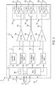
- the controller 12 includes a modulation index unit 100 and a PWM logic circuit 102.
- the modulation index unit 100 and PWM logic circuit 102 can be integrated in the controller 12 as shown in FIG. 3 , or can be implemented as individual hardware controllers.
- the modulation index unit 100 includes a wave generator 104 and a look up table (LUT) 106.
- the modulation index unit 100 receives input signals from the power supply 16, the load 18, and the first, second and third phase output lines 58, 60, 62. Based on one or more of the input signals 16, 18, 58, 60 and 62, the modulation index unit 100 controls the wave generator 104 to output signals 53a, 53b and 53b.
- the output signals 53a, 53b and 53b each include a fundamental signal component, and when necessary to achieve an increased targeted power level, also can include a harmonic signal component.
- the fundamental signal component is a sine wave and the harmonic signal component is the third harmonic of the sine wave.
- the output signals 53a, 53b and 53b are offset in phase from one another by 120 degrees.
- the output signals 53a, 53b and 53b can be modulated with a carrier signal 51 output from carrier wave generator 50.
- the modulation index unit 100 can control the carrier wave generator 50 to dictate the phase, frequency and/or wave-type of the carrier signal 51.
- the carrier signal 51 is a triangle wave.
- the carrier signal 51 is delivered to comparators 54a, 54b and 54c.
- output signal 53a is delivered to comparator 54a
- output signal 53b is delivered to comparator 54b
- output signal 53c is delivered to comparator 54c.
- comparator 54a When the value (i.e., amplitude) of the carrier signal 51 is greater than the value of output signal 53a, comparator 54a outputs a modulated signal 55a, which includes the carrier signal 51 containing the output signal 53a.
- comparator 54b outputs modulated signal 55b, which includes the carrier signal 51 containing the output signal 53b.
- comparator 54c outputs modulated signal 55c, which includes the carrier signal 51 containing the output signal 53c.
- modulated signals 55a, 55b and 55c are delivered to control switch drivers 26a, 26b, 26c, respectively.
- control switch driver 26a In response to receiving modulated signal 55a, control switch driver 26a outputs a first drive signal 27a via buffer 56a having a first voltage value to switch on (i.e., activate) a corresponding switch (e.g., switch 30) and outputs a second drive signal 27b via inverter 56b having a second voltage to switch off (i.e., deactivate) a corresponding switch (e.g., switch 36).
- control switch driver 26b In response to receiving modulated signal 55b, control switch driver 26b outputs a first drive signal 29a via buffer 58a having a first voltage value to switch on (i.e., activate) a corresponding switch (e.g., switch 34) and outputs a second drive signal 29b via inverter 58b having a second voltage to switch off (i.e., deactivate) a corresponding switch (e.g., switch 40).
- control switch driver 26c In response to receiving modulated signal 55c, control switch driver 26c outputs a first drive signal 31a via buffer 60a having a first voltage value to switch on (i.e., activate) a corresponding switch (e.g., switch 38) and outputs a second drive signal 31b via inverter 60b having a second voltage to switch off (i.e., deactivate) a corresponding switch (e.g., switch 32).
- the modulation index unit 100 further determines the modulation index (mi) and controls the PWM logic circuit 102 to generate output drive signals 27a/27b, 29a/29b and 31a/31b that control the switching network 20 of the inverter 14. Unlike conventional power systems, however, the modulation index unit 100 determines the modulation index required to achieve the power demands of the load 18, and controls the PWM logic circuit 102 to control operation of the switching network to gradually inject a harmonic signal on to the first, second and third phase output lines 58, 60, 62, while at the same time reducing the amplitude of the fundamental signal component present on the first, second and third phase output lines 58, 60, 62.
- the modulation index (mi) can be increased above 1.00 to obtain a maximum differential voltage on the first, second and third phase output lines 58, 60, 62 with a minimum amount of harmonic injected into the phase voltages, or common-mode voltages.
- the controller 12 determines various parameters based on the input signals from the power supply 16, the load 18, and the first, second and third phase output lines 58, 60, 62. Accordingly, the modulation index unit 100 can calculate the expected modulation index that is required to achieve the desired voltage and current necessary to achieve the changing power demand of the load 18 based on current feedback inputs (e.g., ireca, irecb, and irecc) associated with the first, second and third phase output lines 58, 60, 62.
- current feedback inputs e.g., ireca, irecb, and irecc
- the PWM logic circuit 102 can control switch drivers 26a, 26b, 26c to generate PWM drive signals 27a/27b, 29a/29b and 31a/31b that are delivered to switches 30, 32, 34, 36, 38, 40 of the inverter switching network 20.
- the modulation index unit 100 can calculate the modulation index based on a reference current (i dc_ref ), current feedback inputs (e.g., irec a , irec b , and irec c ), and phase parameters (e.g., phase a , phase b , and phase c ) associated with the first, second and third phase output lines 58, 60, 62.
- a reference current i dc_ref
- current feedback inputs e.g., irec a , irec b , and irec c
- phase parameters e.g., phase a , phase b , and phase c
- the PWM logic circuit 102 can control the switch drivers 26a, 26b, 26c so as to generate the PWM drive signals 27a/27b, 29a/29b and 31a/31b for driving switches 30, 32, 34, 36, 38, 40 of the inverter switching network 20.
- the modulation index unit 100 can determine a modulation index (mi) required to achieve the power demands of the load 18.
- the modulation index can be defined as the ratio of the peak of a modulating signal or demand fundamental signal component to the peak of a carrier signal.
- the fundamental signal component is a sine wave
- the harmonic is the third harmonic of the sine wave (i.e., the fundamental signal component)
- the carrier signal is a triangle wave.
- the PWM logic circuit 102 controls operation of the switching network 20 to gradually inject the third harmonic on to the first, second and third phase output lines 58, 60, 62, while at the same time reducing the amplitude of the fundamental signal component to generate PWM drive signals 27a/27b, 29a/29b and 31a/31b.
- the amplitude of the fundamental signal component is gradually decreased according to an optimized curve to avoid saturation.
- FIG. 4 illustrates the state of the harmonic 400 (e.g., the third harmonic) generated by switch drivers 26a, 26b, 26c.
- the modulation index unit 100 gradually increases the third harmonic in response to determining the modulation necessary to meet load demands exceeds 1.0). More specifically, prior to the calculated modulation index (mi) exceeding 1.00, the harmonic 400 is 0.0.
- the controller 12 controls the switch drivers 26a, 26b, 26c so as to gradually increase the third harmonic 400 added to the PWM drive signals 27a/27b, 29a/29b and 31a/31b.
- the points of the optimized region 410 can be determined using the LUT 106 stored in the modulation index unit 100.
- modulation index unit 100 can determine the optimized region 410 analytically. For example, the modulation index unit 100 can compute the optimized region 410 based on an equation: 3 2 3 x + 1 3 x + 1 12 x
- the value "x" included in the aforementioned equation (Eq.1) is the ratio of third harmonic to the applied fundamental signal component of the PWM signal, which indicates the minimum amount of the third harmonic required in PWM modulation to generate the required output line voltage/current in the optimized region 410, i.e., the region where 1.125 ⁇ mi ⁇ 1.155.
- the optimization 410 of the injected harmonic 400 facilitates an output differential (line-to-line) voltage of up to 2.0pu (1.732 if without harmonic injection), which in this example is the maximum differential voltage that can be achieved using a third harmonic.
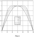
- the actual resulting modulation signal remains below 1.0 as shown in FIG. 6 .
- the resulting PWM drive signals 27a/27b, 29a/29b and 31a/31b can achieve an increase of 1.155 times output line-to-line differential voltage without introducing any harmonics in line-to-line differential voltages, and with minimal level of the third harmonic injected in phase to neutral voltages.
- various non-limiting embodiments of the invention described herein provide a power controller that implements a harmonic injection logic circuit capable of controlling the injection of harmonics into a PWM drive signal in a manner that achieves the maximum voltage output potentially achievable with the DC link while minimizing the level of harmonics introduced to the AC output voltages.
- a maximum level of AC voltage can be applied to a load (e.g., motor) while reducing losses, vibration, noise, and deterioration of the load (e.g., motor performance).
Landscapes
- Engineering & Computer Science (AREA)
- Power Engineering (AREA)
- Inverter Devices (AREA)
Abstract
Description
- Exemplary embodiments are generally related to electrical power systems and more particularly, to power systems for supplying power to an aircraft motor.
- Aircraft power systems commonly employ inverters to convert direct current (DC) power to alternating current (AC) for driving a load such as, for example, a motor. A DC link provides a DC input voltage (typically referred to as the "DC link voltage") to the inverter. However, the output voltage of the inverter using sinusoidal modulation signal has a limited output voltage from an available DC link voltage. Therefore, one or more additional voltage signals can be combined with the sinusoidal modulation signal to increase the inverter output voltage above the maximum available voltage associated with a sinusoidal modulation signal, which in turn introduces additional harmonics (e.g., third and fifth harmonics) into the inverter output voltage.
- According to a non-limiting embodiment, a power system includes a power source configured to generate a direct current (DC) voltage, and an inverter in signal communication with the power source. The inverter is configured to convert the DC voltage to a three-phase alternating current (AC) voltage. At least one switch driver is configured to generate a pulse width modulation (PWM) drive signal that drives the inverter. A controller is in signal communication with the inverter. The controller is configured to determine a modulation index associated with the PWM drive signal and inject a harmonic into the PWM drive signal in response to the modulation index exceeding a modulation index threshold value.
- According to another non-limiting embodiment, a method of supplying power to a load comprises generating a direct current (DC) voltage, and converting, via an inverter, the DC voltage to a three-phase alternating current (AC) voltage. The method further comprises generating, via at least one switch driver, a pulse width modulation (PWM) signal that drives the inverter, and determining, via a controller, a modulation index associated with the PWM drive signal. The method further comprises injecting a harmonic into the PWM drive signal in response to the modulation index exceeding a modulation index threshold value.
- The following descriptions should not be considered limiting in any way. With reference to the accompanying drawings, like elements are numbered alike:
-
FIG. 1 is a block diagram illustrating a power system according to a non-limiting embodiment; -
FIG. 2 is a block diagram of an inverter included in a power system according to a non-limiting embodiment; -
FIG. 3 is a block diagram of a pulse width modulation (PWM) logic circuit implemented in a PWM controller of a power system according to a non-limiting embodiment; -
FIG. 4 is a diagram comparing the injection of an added harmonic to a fundamental signal by conventional inverter systems to the injection of an added harmonic to a fundamental signal by a PWM controller according to a non-limited embodiment of the invention; -
FIG. 5 is a detailed view of a gradually increasing portion of the harmonic added by a PWM controller according to a non-limited embodiment of the invention; and -
FIG. 6 is a diagram depicting resultant modulation signals generated by a PWM controller at different modulation index values to achieve an output phase differential voltage of about 1.155 according to a non-limiting embodiment of the invention. - A detailed description of one or more embodiments of the disclosed apparatus and method are presented herein by way of exemplification and not limitation with reference to the Figures.
- As previously noted, additional voltage signals referred to as "harmonics" can be added to a conventional fundamental sine wave component of an output modulation signal to increase the inverter fundamental output voltage from a given DC link voltage. When using PWM scheme, the modulation index (mi) of the inverter effectively establishes the inverter fundamental output voltage. More specifically, the modulation index is the ratio of the peak of a modulating signal or fundamental signal component to the peak of a higher frequency carrier signal, which is typically a triangle wave. The maximum modulation index is typically set to 1.00 per unit. The inverter fundamental output voltage will not saturate while the modulation index remains in a range of 0.0 to 1.0. The inclusion of additional harmonics, however, can increase the inverter fundamental output voltage without necessarily causing saturation, but at the expense of additional losses, along with increased size, weight and/or deterioration in the performance of the load (e.g., motor). Conventional solutions have aimed to either maintain a fixed triplen harmonic to fundamental ratio resulting in the excessive losses, or to inject less amount of the third harmonic which limits the ability to achieve maximum fundamental voltage output afforded by the DC link.
- Non-limiting embodiments of the invention described herein provides a power controller that implements a harmonic injection logic circuit capable of controlling the injection of a third harmonic into a fundamental signal to generate a modulation signal in a manner that achieves the maximum inverter fundamental voltage output that can be obtained from the DC link while minimizing the amount of harmonics introduced into the inverter output voltage. In this manner, a maximum level output AC voltage can be derived from the given DC link voltage while keeping the third harmonic injection to a minimum.
- With reference now to
FIG. 1 , apower system 10 is illustrated according to a non-limiting embodiment. Thepower system 10 includes acontroller 12, aninverter 14, apower source 16, afilter network 24, and aload 18. Thepower source 16 can be implemented as a direct current (DC) power source, for example, and theload 18 can be any load that accepts AC (alternating current) power such as, for example, amotor 18. Thefilter network 24 is configured to suppress higher order harmonics present in the output power generated by theinverter 14. Thefilter network 24 is also capable of removing the carrier signal from the combined fundamental and harmonic signal, thereby delivering the fundamental signal component and harmonic signal component to theload 18. - The
controller 12 is in signal communication with thepower source 16, theinverter 14 and theload 18. Thecontroller 12 can include memory and an electronic hardware processor configured to execute algorithms and computer-readable program instructions stored in the memory. Accordingly, thecontroller 12 can monitor the voltage levels, current levels and/or temperature levels at various nodes of thesystem 10, and implement various control schemes for operating thepower source 16, theinverter 14 and/or theload 18. Thecontroller 12 can also compute the actual voltage levels and current levels and/or expected voltage levels and current levels based on monitored values and models stored in the memory. - The
inverter 14 includes aswitching network 20. Theswitching network 20 can be constructed, for example, as a six-switch bridge inverter circuit (not shown inFIG. 1 ). The states of the switches can be controlled by thecontroller 12. When the switches of theswitching network 20 are implemented as semiconductor switches (e.g., transistors), thecontroller 12 can include switch drivers (not shown inFIG. 1 ) that are configured to control the signals applied to the gates of respective transistors. In one or more non-limiting embodiments, the transistors include, but are not limited to, bi-polar transistors, insulated gate bipolar transistors (IGBTs), and metal-oxide semiconductor field-effect transistors (MOSFETs). -
FIG. 2 illustrates an example of theswitching network 20 included in theinverter 14 according to a non-limiting embodiment. Theswitching network 20 includes a plurality ofswitches positive rail 42 and a negative (or return)rail 44. The collectors/drains ofswitches positive rail 42 and the emitters/sources ofswitches negative rail 44. The junction or common node (A) of the emitter/source of theswitch 30 and the collector/source of theswitch 36 is connected to a firstphase output line 58 of theinverter switching network 20. The junction or common node (B) of the emitter/source ofswitch 34 and the collector/source ofswitch 40 is connected to a secondphase output line 60 of theswitching network 20. The junction or common node (C) of the emitter/source ofswitch 38 and the collector/drain ofswitch 32 is connected to a thirdphase output line 62 of theswitching network 20. - The bases/gates of
switches drivers output drive signals 27a/27b, 29a/29b and 31a/31b, respectively. In this manner, thecontroller 12 can control theswitches output lines controller 12 can controlswitches phase output line 60 is displaced in phase by 120° from the switching pattern on the firstphase output line 58, and the switching pattern on the thirdphase output line 62 is displaced in phase by 120° with respect to the switching pattern on the secondphase output line 60 and by 240° with respect to the switching pattern on the firstphase output line 58. Furthermore, thecontroller 12, as is known, may control theswitches switches switches - Turning to
FIG. 3 , thecontroller 12 is shown in greater detail. Thecontroller 12 includes amodulation index unit 100 and aPWM logic circuit 102. Themodulation index unit 100 andPWM logic circuit 102 can be integrated in thecontroller 12 as shown inFIG. 3 , or can be implemented as individual hardware controllers. - The
modulation index unit 100 includes awave generator 104 and a look up table (LUT) 106. Themodulation index unit 100 receives input signals from thepower supply 16, theload 18, and the first, second and thirdphase output lines modulation index unit 100 controls thewave generator 104 tooutput signals output signals output signals carrier wave generator 50. Themodulation index unit 100 can control thecarrier wave generator 50 to dictate the phase, frequency and/or wave-type of the carrier signal 51. In one or more examples, the carrier signal 51 is a triangle wave. - The carrier signal 51 is delivered to
comparators output signal 53a is delivered tocomparator 54a,output signal 53b is delivered tocomparator 54b, andoutput signal 53c is delivered tocomparator 54c. When the value (i.e., amplitude) of the carrier signal 51 is greater than the value ofoutput signal 53a,comparator 54a outputs a modulatedsignal 55a, which includes the carrier signal 51 containing theoutput signal 53a. When the value (i.e., amplitude) of the carrier signal 51 is greater than the value ofoutput signal 53b,comparator 54b outputs modulatedsignal 55b, which includes the carrier signal 51 containing theoutput signal 53b. When the value (i.e., amplitude) of the carrier signal 51 is greater than the value ofoutput signal 53c,comparator 54c outputs modulated signal 55c, which includes the carrier signal 51 containing theoutput signal 53c. - The modulated
signals switch drivers signal 55a,control switch driver 26a outputs afirst drive signal 27a viabuffer 56a having a first voltage value to switch on (i.e., activate) a corresponding switch (e.g., switch 30) and outputs asecond drive signal 27b viainverter 56b having a second voltage to switch off (i.e., deactivate) a corresponding switch (e.g., switch 36). In response to receiving modulatedsignal 55b,control switch driver 26b outputs afirst drive signal 29a viabuffer 58a having a first voltage value to switch on (i.e., activate) a corresponding switch (e.g., switch 34) and outputs asecond drive signal 29b viainverter 58b having a second voltage to switch off (i.e., deactivate) a corresponding switch (e.g., switch 40). In response to receiving modulated signal 55c,control switch driver 26c outputs afirst drive signal 31a viabuffer 60a having a first voltage value to switch on (i.e., activate) a corresponding switch (e.g., switch 38) and outputs asecond drive signal 31b viainverter 60b having a second voltage to switch off (i.e., deactivate) a corresponding switch (e.g., switch 32). - The
modulation index unit 100 further determines the modulation index (mi) and controls thePWM logic circuit 102 to generateoutput drive signals 27a/27b, 29a/29b and 31a/31b that control theswitching network 20 of theinverter 14. Unlike conventional power systems, however, themodulation index unit 100 determines the modulation index required to achieve the power demands of theload 18, and controls thePWM logic circuit 102 to control operation of the switching network to gradually inject a harmonic signal on to the first, second and thirdphase output lines phase output lines phase output lines - In one or more non-limiting embodiments, the
controller 12 determines various parameters based on the input signals from thepower supply 16, theload 18, and the first, second and thirdphase output lines modulation index unit 100 can calculate the expected modulation index that is required to achieve the desired voltage and current necessary to achieve the changing power demand of theload 18 based on current feedback inputs (e.g., ireca, irecb, and irecc) associated with the first, second and thirdphase output lines modulation index unit 100, thePWM logic circuit 102 can controlswitch drivers switches inverter switching network 20. - In some non-limiting embodiments, the
modulation index unit 100 can calculate the modulation index based on a reference current (idc_ref), current feedback inputs (e.g., ireca, irecb, and irecc), and phase parameters (e.g., phasea, phaseb, and phasec) associated with the first, second and thirdphase output lines PWM logic circuit 102 can control theswitch drivers switches inverter switching network 20. - As described above, the
modulation index unit 100 can determine a modulation index (mi) required to achieve the power demands of theload 18. The modulation index can be defined as the ratio of the peak of a modulating signal or demand fundamental signal component to the peak of a carrier signal. In one or more examples described herein, the fundamental signal component is a sine wave, the harmonic is the third harmonic of the sine wave (i.e., the fundamental signal component), and the carrier signal is a triangle wave. Based on the determined modulation index, thePWM logic circuit 102 controls operation of theswitching network 20 to gradually inject the third harmonic on to the first, second and thirdphase output lines PWM logic circuit 102 begins to gradually add the third harmonic in response to the modulation index increasing above a modulation index threshold value ranging, for example, from about mi = 1.000 to about mi = 1.125. However, as the third harmonic is gradually added, the amplitude of the fundamental signal component is gradually decreased according to an optimized curve to avoid saturation. -
FIG. 4 , for example, illustrates the state of the harmonic 400 (e.g., the third harmonic) generated byswitch drivers modulation index unit 100 gradually increases the third harmonic in response to determining the modulation necessary to meet load demands exceeds 1.0). More specifically, prior to the calculated modulation index (mi) exceeding 1.00, the harmonic 400 is 0.0. In response to the calculated modulation index exceeding 1.00 (as calculated to satisfy the changing demand of the load 18), thecontroller 12 controls theswitch drivers region 410 to achieve the maximum differential voltage achievable by the minimum harmonic injection. Beginning at mi = 1.125, for example, the magnitude (i.e., amplitude) of the added third harmonic increases exponential and reaches mi = 1.155. - Referring to
FIG. 5 , the optimized region 410 (e.g., an exponential increasing portion) of the harmonic 400 is produced from about mi = 1.125 to about mi = 1.155 to achieve the maximum differential voltage achievable using the third harmonic. Between the modulation index range of about 1.125 and about 1.155 (e.g., 1.125 < mi <1.155), the third harmonic is optimized at each point such that minimum injection is used to achieve the output voltage necessary to satisfy the demand of theload 18. That is, themodulation index unit 100 optimizes the modulation index when the modulation index exceeds 1.125 and reaches the theoretical maximum, e.g., mi = 1.155. In one or more embodiments, the points of the optimizedregion 410 can be determined using theLUT 106 stored in themodulation index unit 100. In other embodiments,modulation index unit 100 can determine the optimizedregion 410 analytically. For example, themodulation index unit 100 can compute the optimizedregion 410 based on an equation:
- The value "x" included in the aforementioned equation (Eq.1) is the ratio of third harmonic to the applied fundamental signal component of the PWM signal, which indicates the minimum amount of the third harmonic required in PWM modulation to generate the required output line voltage/current in the optimized
region 410, i.e., the region where 1.125 < mi < 1.155. - The
optimization 410 of the injected harmonic 400 facilitates an output differential (line-to-line) voltage of up to 2.0pu (1.732 if without harmonic injection), which in this example is the maximum differential voltage that can be achieved using a third harmonic. Unlike conventional power systems, however, the actual resulting modulation signal remains below 1.0 as shown inFIG. 6 . In this manner, the resulting PWM drive signals 27a/27b, 29a/29b and 31a/31b can achieve an increase of 1.155 times output line-to-line differential voltage without introducing any harmonics in line-to-line differential voltages, and with minimal level of the third harmonic injected in phase to neutral voltages. - As described above, various non-limiting embodiments of the invention described herein provide a power controller that implements a harmonic injection logic circuit capable of controlling the injection of harmonics into a PWM drive signal in a manner that achieves the maximum voltage output potentially achievable with the DC link while minimizing the level of harmonics introduced to the AC output voltages. In this manner, a maximum level of AC voltage can be applied to a load (e.g., motor) while reducing losses, vibration, noise, and deterioration of the load (e.g., motor performance).
- The terminology used herein is for the purpose of describing particular embodiments only and is not intended to be limiting of the present disclosure. As used herein, the singular forms "a", "an" and "the" are intended to include the plural forms as well, unless the context clearly indicates otherwise. The term "about" is intended to include the degree of error associated with measurement of the particular quantity based upon the equipment available at the time of filing the application. It will be further understood that the terms "comprises" and/or "comprising," when used in this specification, specify the presence of stated features, integers, steps, operations, elements, and/or components, but do not preclude the presence or addition of one or more other features, integers, steps, operations, element components, and/or groups thereof.
- While the present disclosure has been described with reference to an exemplary embodiment or embodiments, it will be understood by those skilled in the art that various changes may be made without departing from the scope of the invention as defined by the claims. The method operations and/or algorithm(s) recited in the claims can be represented by a flow diagram illustrating the operations, method steps and/or algorithm(s) executed by one or more controllers as described herein. In addition, many modifications may be made to adapt a particular situation or material to the teachings of the present disclosure without departing from the scope of the claims. Therefore, it is intended that the present disclosure not be limited to the particular embodiment disclosed as the best mode contemplated for carrying out this present disclosure, but that the present disclosure will include all embodiments falling within the scope of the claims.
Claims (15)
- A power system comprising:a power source (16) configured to generate a direct current, DC, voltage;an inverter (14) in signal communication with the power source, the inverter configured to convert the DC voltage to a three-phase alternating current, AC, voltage;at least one switch driver (26a, 26b, 26c) configured to generate a pulse width modulation, PWM, drive signal that drives the inverter; anda controller (12) in signal communication with the inverter, the controller configured to determine a modulation index associated with the PWM drive signal and inject a harmonic into the PWM drive signal in response to the modulation index exceeding a modulation index threshold value.
- The power system of claim 1, wherein the threshold value modulation index threshold value is set at a saturation voltage associated with the PWM drive signal and has a value of about 1.125.
- The power system of claim 2, wherein the PWM drive signal includes a fundamental signal component, and optionally wherein the controller (12) decreases an amplitude of the fundamental signal component while increasing an amplitude of the harmonic so as to generate the PWM drive signal.
- The power system of claim 3, wherein a total amplitude of the three-phase AC voltage is increased without saturating the fundamental signal component, and optionally wherein the fundamental signal component is a sine wave and the harmonic is a third harmonic of the sine wave.
- The power system of claim 4, wherein the controller (12) determines the modulation index based on a power demand of a load connected to an output of the inverter.
- The power system of claim 5, wherein the controller (12) determines an optimization region of the harmonic from a first modulation index value to a second modulation index value, and exponentially increases the amplitude of the harmonic within the optimization region.
- The power system of claim 6, wherein the controller (12) optimizes a plurality of voltage values residing in the optimization region of the harmonic, and optionally wherein the controller determines the optimization to be applied to the plurality of voltage values based one or both of a look up table, LUT, stored in memory and an analytical computation.
- A method of supplying power to a load, the method comprising:generating a direct current, DC, voltage;converting, via an inverter (14), the DC voltage to a three-phase alternating current, AC, voltage;generating, via at least one switch driver (26a, 26b, 26c), a pulse width modulation, PWM. signal that drives the inverter;determining, via a controller (12), a modulation index associated with the PWM drive signal; andinjecting a harmonic into the PWM drive signal in response to the modulation index exceeding a modulation index threshold value.
- The method of claim 8, wherein the threshold value modulation index threshold value is set at a saturation voltage associated with the PWM drive signal and has a value of about 1.125.
- The method of claim 9, wherein the PWM drive signal includes a fundamental signal component, and optionally further comprising decreasing, via the controller, an amplitude of the fundamental signal component while increasing an amplitude of the harmonic so as to generate the PWM drive signal.
- The method of claim 10, further comprising increasing a total amplitude of the three-phase AC voltage without saturating the fundamental signal component in response to increasing the amplitude of the harmonic, and optionally wherein the fundamental signal component is a sine wave and the harmonic is a third harmonic of the sine wave.
- The method of claim 11, further comprising, determining, via the controller, the modulation index based on a power demand of a load connected to an output of the inverter.
- The method of claim 12, further comprising:determining, via the controller, an optimization region of the harmonic from a first modulation index value to a second modulation index value; andexponentially increasing the amplitude of the harmonic within the optimization region.
- The method of claim 13, further comprising, optimizing, via the controller, a plurality of voltage values residing in the optimization region of the harmonic.
- The method of claim 14, determining, via the controller, the optimization to be applied to the plurality of voltage values based one or both of a look up table (LUT) stored in memory and an analytical computation.
Applications Claiming Priority (1)
| Application Number | Priority Date | Filing Date | Title |
|---|---|---|---|
| US202063021813P | 2020-05-08 | 2020-05-08 |
Publications (1)
| Publication Number | Publication Date |
|---|---|
| EP3907868A1 true EP3907868A1 (en) | 2021-11-10 |
Family
ID=75887963
Family Applications (1)
| Application Number | Title | Priority Date | Filing Date |
|---|---|---|---|
| EP21173123.7A Withdrawn EP3907868A1 (en) | 2020-05-08 | 2021-05-10 | Over-modulation pulse width modulation with maximum output and minimum harmonics |
Country Status (2)
| Country | Link |
|---|---|
| US (1) | US11456680B2 (en) |
| EP (1) | EP3907868A1 (en) |
Families Citing this family (4)
| Publication number | Priority date | Publication date | Assignee | Title |
|---|---|---|---|---|
| CN112865575B (en) * | 2021-04-13 | 2022-05-24 | 阳光电源股份有限公司 | Inversion control method and application device thereof |
| US11901855B2 (en) * | 2021-06-17 | 2024-02-13 | Rockwell Automation Technologies, Inc. | Polyharmonic flux motor loss increase |
| CN115664237B (en) * | 2022-12-13 | 2023-03-10 | 麦田能源有限公司 | Single-phase inverter system and single-phase inverter control method |
| WO2026034017A1 (en) * | 2024-08-09 | 2026-02-12 | 株式会社Ihi | Motor drive system, control program for motor system, and generator drive system |
Citations (3)
| Publication number | Priority date | Publication date | Assignee | Title |
|---|---|---|---|---|
| JP2005045846A (en) * | 2003-07-22 | 2005-02-17 | Hitachi Ltd | Power converter |
| EP2709261A1 (en) * | 2012-07-03 | 2014-03-19 | Huawei Technologies Co., Ltd. | Inverter and pwm modulation method thereof |
| EP3484044A1 (en) * | 2016-07-05 | 2019-05-15 | Hitachi Automotive Systems, Ltd. | 6-line 3-phase motor, inverter apparatus, and motor system |
Family Cites Families (31)
| Publication number | Priority date | Publication date | Assignee | Title |
|---|---|---|---|---|
| US5450306A (en) * | 1992-12-07 | 1995-09-12 | Square D Company | Closed loop pulse width modulator inverter with volt-seconds feedback control |
| US5623219A (en) * | 1995-11-07 | 1997-04-22 | Karraker; Douglas W. | Maximal voltage three-phase PWM without third harmonic injection |
| US6014497A (en) * | 1997-10-01 | 2000-01-11 | Allen-Bradley Company, Llc | Method and apparatus for determining a critical dwell time for use in motor controls |
| US6023417A (en) * | 1998-02-20 | 2000-02-08 | Allen-Bradley Company, Llc | Generalized discontinuous pulse width modulator |
| US6154378A (en) | 1998-04-29 | 2000-11-28 | Lockheed Martin Corporation | Polyphase inverter with neutral-leg inductor |
| BR9907351A (en) | 1999-12-22 | 2001-08-07 | Ericsson Telecomunicacoees S A | Control method and circuit for three-level three-level elevator rectifier |
| GB0213098D0 (en) * | 2002-06-07 | 2002-07-17 | Trw Ltd | Motor control device |
| GB0422201D0 (en) | 2004-10-07 | 2004-11-03 | Trw Ltd | Motor drive control |
| ES2385095T3 (en) * | 2007-04-20 | 2012-07-18 | Mitsubishi Electric Corporation | Inverter controller |
| JP4858597B2 (en) * | 2008-11-28 | 2012-01-18 | 株式会社デンソー | Rotating machine control device and manufacturing method thereof |
| JP5558752B2 (en) * | 2009-07-30 | 2014-07-23 | 日立オートモティブシステムズ株式会社 | Power converter |
| WO2011099122A1 (en) * | 2010-02-10 | 2011-08-18 | 株式会社 日立製作所 | Power conversion device |
| JP5146478B2 (en) * | 2010-03-18 | 2013-02-20 | 株式会社デンソー | Rotating machine control device |
| JP5120669B2 (en) * | 2010-03-31 | 2013-01-16 | アイシン・エィ・ダブリュ株式会社 | Control device for motor drive device |
| JP5120670B2 (en) * | 2010-03-31 | 2013-01-16 | アイシン・エィ・ダブリュ株式会社 | Control device for motor drive device |
| WO2011135696A1 (en) * | 2010-04-28 | 2011-11-03 | 株式会社 日立製作所 | Power conversion device |
| US8441820B2 (en) | 2010-09-29 | 2013-05-14 | General Electric Company | DC-link voltage balancing system and method for multilevel converters |
| EP2709267B1 (en) * | 2011-05-13 | 2020-08-12 | Hitachi, Ltd. | Drive system for synchronous motor |
| IN2014CN02973A (en) * | 2011-09-30 | 2015-07-03 | Mitsubishi Electric Corp | |
| JP6303354B2 (en) * | 2013-09-19 | 2018-04-04 | 株式会社デンソー | Motor drive device |
| WO2015138744A1 (en) | 2014-03-13 | 2015-09-17 | Qatar Foundation For Education, Science And Community Development | Modulation and control methods for quasi-z-source cascade multilevel inverters |
| US9236828B1 (en) | 2014-07-03 | 2016-01-12 | Rockwell Automation Technologies, Inc. | Methods and power conversion system control apparatus to control IGBT junction temperature at low speed |
| US20160144871A1 (en) | 2014-11-25 | 2016-05-26 | Electro-Motive Diesel, Inc. | Inverter-Based Head End Power System |
| KR102028328B1 (en) * | 2015-04-14 | 2019-10-04 | 엘에스산전 주식회사 | Apparatus for controlling grid-connected inverter |
| KR102009512B1 (en) * | 2015-04-14 | 2019-08-13 | 엘에스산전 주식회사 | Apparatus and method for generating offset voltage of 3-phase inverter |
| DE112015006879T5 (en) * | 2015-09-04 | 2018-05-09 | Mitsubishi Electric Corporation | Power conversion device and heat pump device |
| JP6493164B2 (en) * | 2015-11-06 | 2019-04-03 | 株式会社デンソー | Rotating electric machine drive system |
| EP3637608B1 (en) * | 2017-05-18 | 2022-12-14 | Toshiba Mitsubishi-Electric Industrial Systems Corporation | Power conversion device |
| US10541602B2 (en) * | 2017-10-30 | 2020-01-21 | University Of Florida Research Foundation, Inc. | SPWM with DC offset based on total energy reduction |
| JP6585872B1 (en) * | 2018-10-30 | 2019-10-02 | 東芝三菱電機産業システム株式会社 | Power converter |
| US10784797B1 (en) * | 2019-06-19 | 2020-09-22 | Rockwell Automation Technologies, Inc. | Bootstrap charging by PWM control |
-
2021
- 2021-04-29 US US17/244,178 patent/US11456680B2/en active Active
- 2021-05-10 EP EP21173123.7A patent/EP3907868A1/en not_active Withdrawn
Patent Citations (3)
| Publication number | Priority date | Publication date | Assignee | Title |
|---|---|---|---|---|
| JP2005045846A (en) * | 2003-07-22 | 2005-02-17 | Hitachi Ltd | Power converter |
| EP2709261A1 (en) * | 2012-07-03 | 2014-03-19 | Huawei Technologies Co., Ltd. | Inverter and pwm modulation method thereof |
| EP3484044A1 (en) * | 2016-07-05 | 2019-05-15 | Hitachi Automotive Systems, Ltd. | 6-line 3-phase motor, inverter apparatus, and motor system |
Non-Patent Citations (1)
| Title |
|---|
| ALBATRAN SAHER ET AL: "Minimizing Total Harmonic Distortion of a Two-Level Voltage Source Inverter Using Optimal Third Harmonic Injection", IEEE TRANSACTIONS ON POWER ELECTRONICS, INSTITUTE OF ELECTRICAL AND ELECTRONICS ENGINEERS, USA, vol. 35, no. 3, March 2020 (2020-03-01), pages 3287 - 3297, XP011761811, ISSN: 0885-8993, [retrieved on 20191219], DOI: 10.1109/TPEL.2019.2932139 * |
Also Published As
| Publication number | Publication date |
|---|---|
| US20210351689A1 (en) | 2021-11-11 |
| US11456680B2 (en) | 2022-09-27 |
Similar Documents
| Publication | Publication Date | Title |
|---|---|---|
| US11456680B2 (en) | Over-modulation pulse width modulation with maximum output and minimum harmonics | |
| US6534949B2 (en) | Motor drive converter and method with neutral point drift compensation | |
| CN103368488B (en) | For the controller of multi-phase rotary device | |
| KR102009509B1 (en) | Apparatus and method for generating offset voltage of 3-phase inverter | |
| KR100655917B1 (en) | PWM pulse control method | |
| JP3178075B2 (en) | Power converter control device and electric vehicle control device | |
| US20070133242A1 (en) | Method and apparatus for controlling voltage linearity of voltage source inverters | |
| JP5126550B2 (en) | Matrix converter | |
| KR970055166A (en) | NPC Inverter Control System | |
| US11368109B2 (en) | Power conversion system with PWM carrier transition smoothing and autotuning | |
| EP3082247A2 (en) | Offset voltage generator and method for generating an offset voltage of three-phase inverter | |
| US12132429B2 (en) | Power conversion device and motor system | |
| US11979104B2 (en) | Rotary electric machine control apparatus | |
| US9923505B2 (en) | Methods and systems for controlling an electric motor | |
| US11863098B2 (en) | Multi-level inverter | |
| US11984830B2 (en) | Inverter with switch control and a method of controlling an inverter | |
| US11646676B2 (en) | Method and apparatus for generating a three-phase voltage | |
| JP2923727B2 (en) | Power converter | |
| JP4277360B2 (en) | 3-level inverter controller | |
| JP2005237194A (en) | Electric vehicle control device | |
| EP4478599A1 (en) | Method for overmodulating a multi-phase inverter, computer program product and a multi-phase inverter | |
| US20250167697A1 (en) | Multi-phase power converter control | |
| JP2002058251A (en) | Control device for power converter | |
| JPH1052062A (en) | Control device for 3-level inverter | |
| US20260019007A1 (en) | Model predictive control for converter with filter cells based on offline-computed pulse patterns and online cell balancing |
Legal Events
| Date | Code | Title | Description |
|---|---|---|---|
| PUAI | Public reference made under article 153(3) epc to a published international application that has entered the european phase |
Free format text: ORIGINAL CODE: 0009012 |
|
| STAA | Information on the status of an ep patent application or granted ep patent |
Free format text: STATUS: THE APPLICATION HAS BEEN PUBLISHED |
|
| AK | Designated contracting states |
Kind code of ref document: A1 Designated state(s): AL AT BE BG CH CY CZ DE DK EE ES FI FR GB GR HR HU IE IS IT LI LT LU LV MC MK MT NL NO PL PT RO RS SE SI SK SM TR |
|
| B565 | Issuance of search results under rule 164(2) epc |
Effective date: 20210907 |
|
| STAA | Information on the status of an ep patent application or granted ep patent |
Free format text: STATUS: REQUEST FOR EXAMINATION WAS MADE |
|
| 17P | Request for examination filed |
Effective date: 20220510 |
|
| RBV | Designated contracting states (corrected) |
Designated state(s): AL AT BE BG CH CY CZ DE DK EE ES FI FR GB GR HR HU IE IS IT LI LT LU LV MC MK MT NL NO PL PT RO RS SE SI SK SM TR |
|
| STAA | Information on the status of an ep patent application or granted ep patent |
Free format text: STATUS: EXAMINATION IS IN PROGRESS |
|
| 17Q | First examination report despatched |
Effective date: 20230418 |
|
| STAA | Information on the status of an ep patent application or granted ep patent |
Free format text: STATUS: THE APPLICATION HAS BEEN WITHDRAWN |
|
| 18W | Application withdrawn |
Effective date: 20250613 |