EP3907819B1 - Secondary battery - Google Patents
Secondary battery Download PDFInfo
- Publication number
- EP3907819B1 EP3907819B1 EP20857179.4A EP20857179A EP3907819B1 EP 3907819 B1 EP3907819 B1 EP 3907819B1 EP 20857179 A EP20857179 A EP 20857179A EP 3907819 B1 EP3907819 B1 EP 3907819B1
- Authority
- EP
- European Patent Office
- Prior art keywords
- conductive
- area
- electrode
- layer
- secondary battery
- Prior art date
- Legal status (The legal status is an assumption and is not a legal conclusion. Google has not performed a legal analysis and makes no representation as to the accuracy of the status listed.)
- Active
Links
Images


Classifications
-
- H—ELECTRICITY
- H01—ELECTRIC ELEMENTS
- H01M—PROCESSES OR MEANS, e.g. BATTERIES, FOR THE DIRECT CONVERSION OF CHEMICAL ENERGY INTO ELECTRICAL ENERGY
- H01M50/00—Constructional details or processes of manufacture of the non-active parts of electrochemical cells other than fuel cells, e.g. hybrid cells
- H01M50/10—Primary casings; Jackets or wrappings
- H01M50/102—Primary casings; Jackets or wrappings characterised by their shape or physical structure
- H01M50/105—Pouches or flexible bags
-
- H—ELECTRICITY
- H01—ELECTRIC ELEMENTS
- H01M—PROCESSES OR MEANS, e.g. BATTERIES, FOR THE DIRECT CONVERSION OF CHEMICAL ENERGY INTO ELECTRICAL ENERGY
- H01M10/00—Secondary cells; Manufacture thereof
- H01M10/04—Construction or manufacture in general
- H01M10/045—Cells or batteries with folded plate-like electrodes
-
- H—ELECTRICITY
- H01—ELECTRIC ELEMENTS
- H01M—PROCESSES OR MEANS, e.g. BATTERIES, FOR THE DIRECT CONVERSION OF CHEMICAL ENERGY INTO ELECTRICAL ENERGY
- H01M4/00—Electrodes
- H01M4/02—Electrodes composed of, or comprising, active material
- H01M4/64—Carriers or collectors
- H01M4/66—Selection of materials
- H01M4/665—Composites
- H01M4/667—Composites in the form of layers, e.g. coatings
-
- H—ELECTRICITY
- H01—ELECTRIC ELEMENTS
- H01M—PROCESSES OR MEANS, e.g. BATTERIES, FOR THE DIRECT CONVERSION OF CHEMICAL ENERGY INTO ELECTRICAL ENERGY
- H01M50/00—Constructional details or processes of manufacture of the non-active parts of electrochemical cells other than fuel cells, e.g. hybrid cells
- H01M50/10—Primary casings; Jackets or wrappings
- H01M50/183—Sealing members
-
- H—ELECTRICITY
- H01—ELECTRIC ELEMENTS
- H01M—PROCESSES OR MEANS, e.g. BATTERIES, FOR THE DIRECT CONVERSION OF CHEMICAL ENERGY INTO ELECTRICAL ENERGY
- H01M50/00—Constructional details or processes of manufacture of the non-active parts of electrochemical cells other than fuel cells, e.g. hybrid cells
- H01M50/50—Current conducting connections for cells or batteries
- H01M50/531—Electrode connections inside a battery casing
- H01M50/536—Electrode connections inside a battery casing characterised by the method of fixing the leads to the electrodes, e.g. by welding
-
- H—ELECTRICITY
- H01—ELECTRIC ELEMENTS
- H01M—PROCESSES OR MEANS, e.g. BATTERIES, FOR THE DIRECT CONVERSION OF CHEMICAL ENERGY INTO ELECTRICAL ENERGY
- H01M50/00—Constructional details or processes of manufacture of the non-active parts of electrochemical cells other than fuel cells, e.g. hybrid cells
- H01M50/50—Current conducting connections for cells or batteries
- H01M50/531—Electrode connections inside a battery casing
- H01M50/538—Connection of several leads or tabs of wound or folded electrode stacks
-
- Y—GENERAL TAGGING OF NEW TECHNOLOGICAL DEVELOPMENTS; GENERAL TAGGING OF CROSS-SECTIONAL TECHNOLOGIES SPANNING OVER SEVERAL SECTIONS OF THE IPC; TECHNICAL SUBJECTS COVERED BY FORMER USPC CROSS-REFERENCE ART COLLECTIONS [XRACs] AND DIGESTS
- Y02—TECHNOLOGIES OR APPLICATIONS FOR MITIGATION OR ADAPTATION AGAINST CLIMATE CHANGE
- Y02E—REDUCTION OF GREENHOUSE GAS [GHG] EMISSIONS, RELATED TO ENERGY GENERATION, TRANSMISSION OR DISTRIBUTION
- Y02E60/00—Enabling technologies; Technologies with a potential or indirect contribution to GHG emissions mitigation
- Y02E60/10—Energy storage using batteries
-
- Y—GENERAL TAGGING OF NEW TECHNOLOGICAL DEVELOPMENTS; GENERAL TAGGING OF CROSS-SECTIONAL TECHNOLOGIES SPANNING OVER SEVERAL SECTIONS OF THE IPC; TECHNICAL SUBJECTS COVERED BY FORMER USPC CROSS-REFERENCE ART COLLECTIONS [XRACs] AND DIGESTS
- Y02—TECHNOLOGIES OR APPLICATIONS FOR MITIGATION OR ADAPTATION AGAINST CLIMATE CHANGE
- Y02P—CLIMATE CHANGE MITIGATION TECHNOLOGIES IN THE PRODUCTION OR PROCESSING OF GOODS
- Y02P70/00—Climate change mitigation technologies in the production process for final industrial or consumer products
- Y02P70/50—Manufacturing or production processes characterised by the final manufactured product
Definitions
- the present disclosure relates to the field of battery technology, in particular to a secondary battery.
- a lithium-ion battery is widely used in portable electronic devices, such as a mobile phone and a notebook, and an electric vehicle, such as an electric car and an electric bicycle, due to their high energy density, high power density, many cycles of use, and long storage time.
- the electrode members of the lithium ion battery are usually made of metal materials.
- a positive electrode member is usually made of aluminum foil
- a negative electrode member is usually made of copper foil.
- the positive electrode member and the negative electrode member will be short-circuited, causing fire and explosion of the lithium ion battery.
- the electrode comprises a multilayered collector assembly having a multilayered portion that includes an insulation layer and two electrically conductive layers disposed on opposite sides of the insulation layer, and a conductive portion made of an electrically conductive material, connected to the two conductive layers and extending therefrom more toward a side end of the electrode than a side end of the insulation layer so as to be electrically connected to the electrode terminal; and a pair of active material layers disposed on opposite sides of the multilayered portion.
- the pole piece includes a current collecting body, an active material layer, a conducting structure and a first protective layer.
- the current collecting body includes an insulating layer and a conducting layer provided on a surface of the insulating layer.
- the conducting layer has a main part and a projection part connected with the main part. A surface of the main part away from the insulating layer is covered by the active material layer, and a surface of the projection part away from the insulating layer is not covered by the active material layer.
- the conducting structure and the projection part are connected with each other by welding to form a welding area.
- the first protective layer has elasticity and is provided at a side of the projection part away from the insulating layer and located between the welding area and the active material layer.
- the secondary cell includes said pole piece.
- a part of the insulating layer corresponding to the projection part and the projection part form an electric guide portion.
- a plurality of electric guide portions are stacked and the conducting structure is provided between per two adjacent electric guide portions.
- the first protective layer and the projection part provided to be corresponded to the first protective layer are bent relative to the main part.
- a purpose of the present disclosure is to provide a secondary battery that can reduce a risk of short circuit and increase energy density.
- the present disclosure provides a secondary battery, comprising an electrode assembly, a packaging bag, and electrode leads.
- the electrode assembly is accommodated in the packaging bag and comprises a first electrode member, a second electrode member and a separator that separates the first electrode member from the second electrode member.
- the first electrode member comprises an insulating substrate, a conductive layer, an active material layer and a conductive structure.
- the conductive layer is provided on a surface of the insulating substrate, the conductive layer is provided with a first portion and a second portion extending from the first portion, the first portion is coated with the active material layer, the second portion is not coated with the active material layer, and the conductive structure is welded to the second portion to form a first welding area.
- the electrode leads are connected to the conductive structure and extend to an outside of the packaging bag.
- a portion of the insulating substrate corresponding to the first portion and the first portion form a main body, and a portion of the insulating substrate corresponding to the second portion and the second portion form an electric guide portion.
- the electric guide portion is provided with an inclined area arranged obliquely with respect to the main body, and the first welding area is at least partially located in the inclined area.
- the first welding area and the first portion are spaced apart along an extension direction of the electric guide portion.
- the electrical guide portion is also provided with a transition area connected between the inclined area and the main body. The inclined area is bent toward the electrode leads relative to the transition area.
- a surface of the transition area is not covered by the conductive structure.
- the conductive layers are arranged on opposite side surfaces of the insulating substrate.
- the conductive structure comprises a first conductive member and a second conductive member connected to each other.
- the first welding area comprises a first sub-welding area and a second sub-welding area.
- the first conductive member is welded to an area of the second portion on a side surface of the insulating substrate to form the first sub-welding area
- the second conductive member is welded to an area of the second portion on the other side surface of the insulating substrate to form the second sub-welding area.
- the first conductive member extends beyond the second conductive member in a direction away from the main body, and a portion of the first conductive member beyond the second conductive member is welded to the electrode leads.
- the first conductive member comprises a first connection portion and a second connection portion.
- the first connection portion is welded to the second portion to form the first sub-welding area, and an end of the first connection portion away from the main body extends beyond the second portion.
- the second connection portion extends from the end of the first connection portion away from the main body, is bent relative to the first connection portion, and is welded to the electrode lead.
- the second conductive member is welded to an area of the first connection portion beyond the second portion.
- multiple electrical guide portions are provided and arranged along a thickness direction of the electrode assembly, multiple conductive structures are provided, and each electrical guide portion is connected to a corresponding conductive structure.
- An angle between the inclined area of the outermost electrical guide portion and the main body is from 100 degrees to 160 degrees in the thickness direction of the electrode assembly.
- the packaging bag is provided with a top wall and a first side wall, the top wall is located on a side of the electrode assembly along the thickness direction, and the first side wall extends from an edge of the top wall and is located on a side of the electric guide portion away from the main body.
- the first side wall is arranged obliquely with respect to the top wall, and an angle between the first side wall and the top wall is smaller than the angle between the inclined area of the outermost electrical guide portion and the main body.
- a surface of the first welding area is provided with an insulating glue. Beneficial effects of the present disclosure are as follows: a thickness of the conductive layer can be reduced by providing the insulating substrate in the present disclosure.
- the conductive layer When a foreign object pierces the electrode member of the secondary battery, as the conductive layer has a small thickness, the conductive layer generates a small burr at a part pierced by the foreign object, and it is difficult to pierce the separator, thereby reducing a risk of short circuit and improving safety performance.
- space occupied the first welding area is reduced and energy density of the secondary battery is improved by the first welding area obliquely arranged.
- the terms “first”, “second”, “third” and the like are used for descriptive purposes only and are not to be construed as indicating or implying relative importance; the meaning of "a plurality” and the like is two or more (including two).
- the term “connected” is to be understood broadly, and may be, for example, a fixed connection, a detachable connection, an integral connection, an electric connection or a signal connection; the term “connected” can be a direct connection or indirect connection through an intermediate medium.
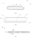
- the secondary battery of the present disclosure includes an electrode assembly 1, a packaging bag 2 and electrode leads 3.
- the electrode assembly 1 is a core component of the secondary battery to realize the charge and discharge function.
- the electrode assembly 1 includes a first electrode member 11, a second electrode member 12 and a separator 13.
- the separator 13 separates the first electrode member 11 and the second electrode member 12.
- the electrode assembly 1 is accommodated in the packaging bag 2.
- the electrode assembly 1 may be in a wound structure.
- One first electrode member 11 and one second electrode member 12 are provided, and the first electrode member 11 and the second electrode member 12 are in a belt-shaped structure.
- the first electrode member 11, the separator 13, and the second electrode member 12 are sequentially stacked and wound two or more turns to form the electrode assembly 1.
- the electrode assembly 1 is flat.
- the packaging bag 2 includes two layers of packaging films 21.
- the two layers of packaging films 21 are stacked along a thickness direction Z.
- at least one layer of packaging film 21 is provided with a cavity via stamping, and the electrode assembly 1 is located between the two layers of packaging films 21 and is accommodated in the cavity.
- each packaging film 21 includes a protective layer 211, a metal layer 212, and a connection layer 213.
- the protective layer 211 and the connection layer 213 are disposed on different sides of the metal layer 212.
- the protective layer 211 may be fixed to a surface of the metal layer 212 away from the electrode assembly 1 via an adhesive.
- the connection layer 213 may be fixed to a surface of the metal layer 212 close to the electrode assembly 1 via an adhesive.
- Material of the protective layer 211 may be nylon or polyethylene terephthalate.
- Material of the metal layer 212 may be aluminum foil or steel foil.
- Material of the connection layer 213 may be polypropylene.
- each packaging film 21 includes a top wall 214 and a plurality of side walls, and the top wall 214 is located on a side of the electrode assembly 1 along the thickness direction Z.
- a plurality of side walls extend from an edge of the top wall 214.
- the top wall 214 and the plurality of side walls enclose a cavity for accommodating the electrode assembly 1.
- Each packaging film 21 also includes an extension wall 217.
- the extension wall 217 extends from the edge of each of the side walls away from the top wall 214 and surrounds outside of the cavity.
- connection layer 213 of the two layers of packaging films 21 is directly or indirectly melted and connected together at the extension wall 217 by heat pressing, thereby forming the sealed packaging bag 2.
- the connection layer 213 is melted and compressed. Therefore, after the heat pressing, a thickness of the seal portion 22 is less than a sum of a thicknesses of the two layers of packaging films 21 before the heat pressing.
- the electrode leads 3 are connected to the electrode assembly 1, pass through the seal portion 22 and extends to the outside of the packaging bag 2. Exemplarily, two electrode leads 3 may be provided. One electrode lead 3 is electrically connected to the first electrode member 11, and the other electrode lead 3 is electrically connected to the second electrode member 12. The two electrode leads 3 connect the electrode assembly 1 with other components outside the packaging bag 2 so as to realize charging and discharging of the electrode assembly 1.
- Material of the electrode leads 3 can be aluminum, nickel or copper with nickel plated.
- the two electrode leads 3 can protrude from different ends of the packaging bag 2 along a length direction X, or can protrude from the same end of the packaging bag 2 along the length direction X.
- the electrode leads 3 are in a sheet shape and substantially parallel to the length direction X.
- the electrode leads 3 pass between the two layers of packaging films 21. And as the connection layer 213 is thin, the electrode leads 3 are easily in contact with the metal layer 212, which causes a safety risk. Therefore, the secondary battery of the present disclosure is provided with the insulator 4.
- two insulators 4 may be provided.
- the two insulators 4 separate each of the two electrode leads 3 from the seal portion 22, respectively.
- Each insulator 4 surrounds outside of a corresponding electrode lead 3.
- a part of the insulator 4 is clamped between the two layers of packaging films 21 to separate the electrode lead 3 from the packaging film 21 and reduce the risk of the electrode lead 3 contacting the metal layer 212.
- Material of the insulator 4 may be polypropylene. As a part of the insulator 4 is clamped between the two layers of packaging films 21, when the two layers of packaging film 21 are heat-pressed, the connection layer 213 of the two layers of packaging films 21 will be melted and connected to the insulator 4.
- the first electrode member 11 includes an insulating substrate 111, a conductive layer 112, an active material layer 113, and a conductive structure 114.
- Material of the insulating substrate 111 may be a PET (polyethylene terephthalate) film or a PP (polypropylene) film.
- the conductive layer 112 is disposed on a surface of the insulating substrate 111.
- Material of the conductive layer 112 is selected from at least one of metal conductive material and carbon-based conductive material.
- the metal conductive material may be at least one of aluminum, copper, nickel, titanium, silver, nickel-copper alloy, and aluminum-zirconium alloy.
- the carbon-based conductive material may be at least one of graphite, acetylene black, graphene, and carbon nanotubes.
- the conductive layer 112 may be formed on the surface of the insulating substrate 111 by at least one of vapor deposition and electroless plating. Among them, the vapor deposition method includes physical vapor deposition (PVD), such as thermal evaporation deposition.
- PVD physical vapor deposition
- the conductive layer 112 includes a first portion 112a and a second portion 112b extending from the first portion 112a.
- the first portion 112a is coated with the active material layer 113, and the second portion 112b is not coated with the active material layer 113.
- the active material layer 113 may be provided on a surface of the conductive layer 112 by coating. Active materials (such as lithium manganate, lithium iron phosphate), adhesives, conductive agents, and solvents can be made into a slurry, and then the slurry can be coated on the surface of the conductive layer 112. The slurry is cured to form the active material layer 113.
- Active materials such as lithium manganate, lithium iron phosphate
- a thickness of the insulating substrate 111 may be from 1 micron ( ⁇ m) to microns ( ⁇ m), and a thickness of the conductive layer 112 may be from 0.1 micron ( ⁇ m) to 10 microns ( ⁇ m). Since the conductive layer 112 is relatively thin, burrs generated by the conductive layer 112 during cutting of the first electrode member 11 are relatively small. Thus it is difficult to pierce the separator 13 with a thickness of more than ten microns, thereby reducing a risk of short circuit and improving safety performance.
- the conductive layer 112 when a foreign object pierces the first electrode member 11 of the secondary battery, since the thickness of the conductive layer 112 is small, the conductive layer 112 generates less burrs at a part pierced by the foreign object, and it is difficult to pierce the separator 13 so the risk of short circuit is reduced and the safety performance is improved.
- a portion of the insulating substrate 111 corresponding to the first portion 112a and the first portion 112a form a main body P1.
- a portion of the insulating substrate 111 corresponding to the second portion 112b and the second portion 112b form an electrical guide portion P2.
- a plurality of electric guide portions P2 may be provided. Referring to FIGS. 3 and 4 , after the electrode assembly 1 is wound into shape, the plurality of electrical guide portions P2 are arranged along the thickness direction Z.
- the conductive structure 114 is welded to the second portion 112b and forms the first welding area W1.
- the first welding area W1 may be formed by ultrasonic welding.
- the electrode lead 3 is connected to the conductive structure 114 and extends to the outside of the packaging bag 2.
- the electrical guide portion P2 includes an inclined area P21 that is inclined with respect to the main body P1.
- the main body P1 is substantially parallel to the length direction X, and the inclined area P21 is inclined with respect to the length direction X.
- a first welding area W1 is at least partially located in the inclined area P21.
- the conductive structure 114 is welded to an area of the second portion 112b located in the inclined area P21.
- the first welding area is inclined with respect to the main body P1.
- the first welding area W1 has poor flexibility and is difficult to be bent. Therefore, if the entire first welding area W1 is parallel to the length direction X, the first welding area W1 will occupy a larger space in the length direction X, which affects the energy density.
- the first welding area W1 is arranged obliquely, so space occupied by the first welding area W1 in the length direction X can be reduced, and the energy density of the secondary battery can be improved.
- the first welding area W1 is spaced apart from the first portion 112a.
- the first welding area W1 is separated from the first portion 112a by a distance.
- An area of the second portion 112b located between the first welding area W1 and the first portion 112a can be bent, so the first welding area W1 is arranged obliquely.
- the electrical guide portion P2 also includes a transition area P22.
- the transition area P22 is connected between the inclined area P21 and the main body P1. With respect to the transition area P22, the inclined area P21 is bent toward the electrode lead 3.
- a distance between a bending part of the electrical guide part P2 and the active material layer 113 can be ensured, a stress at a connection of the first portion 112a and the second portion 112b when the electrical guide portion P2 is bent can be reduced, and a risk of falling off of the active material layer 113 is reduced.
- a surface of the transition area P22 is not covered by the conductive structure 114. In this way, it is possible to avoid bending the conductive structure 114 when bending the electrical guide portion P2, thereby reducing the bending strength.
- the conductive layers 112 are disposed on opposite side surfaces of the insulating substrate 111.
- the conductive layers 112 located on both sides of the insulating substrate 111 are separated by the insulating substrate 111. Current between the conductive layers 112 cannot be passed directly.
- the conductive structure 114 of the present disclosure is connected to each of the conductive layers 112 located at both sides of the insulating substrate 111. Referring to FIGS. 4 and 10 , the conductive structure 114 includes a first conductive member 1141 and a second conductive member 1142. The first conductive member 1141 is connected to the second conductive member 1142.
- the first welding area W1 includes a first sub-welding area W11 and a second sub-welding area W12.
- the first conductive member 1141 is welded to an area of the second portion 112b on a side surface of the insulating substrate 111 to form the first sub-welding area W11.
- the second conductive member 1142 is welded to an area of a surface of the second portion 112b on the other side surface of the insulating substrate 111 to form the second sub-welding area W12. Both the first sub-welding area W11 and the second sub-welding area W12 are inclined with respect to the main body P1.
- the first conductive member 1141 and the second conductive member 1142 can collect currents on the conductive layers 112 located on both sides of the insulating substrate 111 and transmit them to the electrode lead 3, thereby improving the overcurrent capability.
- the first conductive member 1141 extends beyond the second conductive member 1142, and a portion of the first conductive member 1141 beyond the second conductive member 1142 is welded to the electrode lead 3.
- the first conductive member 1141 includes a first connection portion 1141a and a second connection portion 1141b.
- the first connection portion 1141a is welded to the second portion 112b to form the first sub-welding area W11, and an end of the first connection portion 1141a away from the main body P1 extends beyond the second portion 112b.
- the second connection portion 1141b extends from an end of the first connection portion 1141 a away from the main body P1 and is bent relative to the first connection portion 1141a, and the second connection portion 1141b is welded to the electrode lead 3.
- the second conductive member 1142 is welded to an area of the first connection portion 1141a beyond the second portion 112b.
- the second connection portion 1141b is substantially parallel to the electrode lead 3.
- the first connection portion 1141a is inclined with respect to the electrode lead 3. In the present disclosure, when the first conductive member 1141 is bent, the second conductive member 1142 does not need to bent, so bending difficulty is reduced.
- each electrical guide portion P2 is connected to a corresponding conductive structure 114.
- the second connection portion 1141b of the first conductive member 1141 of the plurality of conductive structures 114 is welded to the electrode lead 3 and forms the second welding area W2.
- the second conductive member 1142 is welded to the first connection portion 1141a and forms a third welding area W3.
- the third welding area W3 is arranged obliquely with respect to the length direction X, so the space occupied by the third welding area W3 in the length direction X is reduced.
- the second welding area W2 is formed, there is no need to weld the second conductive member 1142 of the plurality of conductive structures 114 to the electrode lead 3, so the welding difficulty is reduced and space is saved.
- an angle ⁇ is between the inclined area P21 of the outermost electrical guide portion P2 and the main body P1.
- the larger the value of ⁇ the larger the space occupied by the inclined area P21 and the first welding area W1 in the length direction X, and the lower the degree of bending of the inclined area P21 with respect to the main body P1.
- the smaller the value of ⁇ the smaller the space occupied by the inclined area P21 and the first welding area W1 in the length direction X, and the higher the degree of bending of the inclined area P21 relative to the main body P1.
- the value of ⁇ can be from 100 degrees to 160 degrees.
- the plurality of side walls of the packaging film 21 include a first side wall 215 and a second side wall 216.
- the first side wall 215 and the second side wall 216 are located on different sides of the electrode assembly 1 along the length direction X.
- the first side wall 215 is located on a side of the electrical guide portion P2 away from the main body P1.
- the first side wall 215 is inclined with respect to the top wall 214, and an angle ⁇ is between the first side wall 215 and the top wall 214.
- ⁇ is between the first side wall 215 and the top wall 214.
- the value of ⁇ is smaller than the value of ⁇ to reduce the risk of the first welding area W1 piercing the first side wall 215.
- an insulating glue 115 is provided on the surface of the first welding area W1.
- the insulating glue 115 can cover the burrs on the surface of the first welding area W1, so the risk of the first welding area W1 piercing the packaging film 21 or other components is reduced.
Landscapes
- Chemical & Material Sciences (AREA)
- Chemical Kinetics & Catalysis (AREA)
- Electrochemistry (AREA)
- General Chemical & Material Sciences (AREA)
- Engineering & Computer Science (AREA)
- Manufacturing & Machinery (AREA)
- Composite Materials (AREA)
- Materials Engineering (AREA)
- Connection Of Batteries Or Terminals (AREA)
Description
- The present disclosure relates to the field of battery technology, in particular to a secondary battery.
- As a secondary battery, a lithium-ion battery is widely used in portable electronic devices, such as a mobile phone and a notebook, and an electric vehicle, such as an electric car and an electric bicycle, due to their high energy density, high power density, many cycles of use, and long storage time.
- The electrode members of the lithium ion battery are usually made of metal materials. For example, a positive electrode member is usually made of aluminum foil, and a negative electrode member is usually made of copper foil. However, in a nail penetration experiment, the positive electrode member and the negative electrode member will be short-circuited, causing fire and explosion of the lithium ion battery.
- D1 (
EP 2 026 402 A1 - D2 (
CN 208 507 818 U ) discloses a secondary cell and pole piece thereof. The pole piece includes a current collecting body, an active material layer, a conducting structure and a first protective layer. The current collecting body includes an insulating layer and a conducting layer provided on a surface of the insulating layer. The conducting layer has a main part and a projection part connected with the main part. A surface of the main part away from the insulating layer is covered by the active material layer, and a surface of the projection part away from the insulating layer is not covered by the active material layer. The conducting structure and the projection part are connected with each other by welding to form a welding area. The first protective layer has elasticity and is provided at a side of the projection part away from the insulating layer and located between the welding area and the active material layer. The secondary cell includes said pole piece. A part of the insulating layer corresponding to the projection part and the projection part form an electric guide portion. A plurality of electric guide portions are stacked and the conducting structure is provided between per two adjacent electric guide portions. The first protective layer and the projection part provided to be corresponded to the first protective layer are bent relative to the main part. - In view of problems in the background art, a purpose of the present disclosure is to provide a secondary battery that can reduce a risk of short circuit and increase energy density.
- To achieve the above purpose, the present disclosure provides a secondary battery, comprising an electrode assembly, a packaging bag, and electrode leads. The electrode assembly is accommodated in the packaging bag and comprises a first electrode member, a second electrode member and a separator that separates the first electrode member from the second electrode member. The first electrode member comprises an insulating substrate, a conductive layer, an active material layer and a conductive structure. The conductive layer is provided on a surface of the insulating substrate, the conductive layer is provided with a first portion and a second portion extending from the first portion, the first portion is coated with the active material layer, the second portion is not coated with the active material layer, and the conductive structure is welded to the second portion to form a first welding area. The electrode leads are connected to the conductive structure and extend to an outside of the packaging bag. A portion of the insulating substrate corresponding to the first portion and the first portion form a main body, and a portion of the insulating substrate corresponding to the second portion and the second portion form an electric guide portion. The electric guide portion is provided with an inclined area arranged obliquely with respect to the main body, and the first welding area is at least partially located in the inclined area. The first welding area and the first portion are spaced apart along an extension direction of the electric guide portion. The electrical guide portion is also provided with a transition area connected between the inclined area and the main body. The inclined area is bent toward the electrode leads relative to the transition area.
- In some embodiments, a surface of the transition area is not covered by the conductive structure.
- In some embodiments, the conductive layers are arranged on opposite side surfaces of the insulating substrate. The conductive structure comprises a first conductive member and a second conductive member connected to each other. The first welding area comprises a first sub-welding area and a second sub-welding area. The first conductive member is welded to an area of the second portion on a side surface of the insulating substrate to form the first sub-welding area, and the second conductive member is welded to an area of the second portion on the other side surface of the insulating substrate to form the second sub-welding area.
- In some embodiments, the first conductive member extends beyond the second conductive member in a direction away from the main body, and a portion of the first conductive member beyond the second conductive member is welded to the electrode leads.
- In some embodiments, the first conductive member comprises a first connection portion and a second connection portion. The first connection portion is welded to the second portion to form the first sub-welding area, and an end of the first connection portion away from the main body extends beyond the second portion. The second connection portion extends from the end of the first connection portion away from the main body, is bent relative to the first connection portion, and is welded to the electrode lead. The second conductive member is welded to an area of the first connection portion beyond the second portion.
- In some embodiments, multiple electrical guide portions are provided and arranged along a thickness direction of the electrode assembly, multiple conductive structures are provided, and each electrical guide portion is connected to a corresponding conductive structure. An angle between the inclined area of the outermost electrical guide portion and the main body is from 100 degrees to 160 degrees in the thickness direction of the electrode assembly.
- In some embodiments, the packaging bag is provided with a top wall and a first side wall, the top wall is located on a side of the electrode assembly along the thickness direction, and the first side wall extends from an edge of the top wall and is located on a side of the electric guide portion away from the main body. The first side wall is arranged obliquely with respect to the top wall, and an angle between the first side wall and the top wall is smaller than the angle between the inclined area of the outermost electrical guide portion and the main body. In some embodiments, a surface of the first welding area is provided with an insulating glue. Beneficial effects of the present disclosure are as follows: a thickness of the conductive layer can be reduced by providing the insulating substrate in the present disclosure. When a foreign object pierces the electrode member of the secondary battery, as the conductive layer has a small thickness, the conductive layer generates a small burr at a part pierced by the foreign object, and it is difficult to pierce the separator, thereby reducing a risk of short circuit and improving safety performance. In the present disclosure, space occupied the first welding area is reduced and energy density of the secondary battery is improved by the first welding area obliquely arranged.
- In order to explain technical solutions of embodiments of the present disclosure more clearly, drawings that need to be used in the embodiments of the present disclosure will be briefly introduced below. Obviously, the drawings described below are only some embodiments of the present disclosure. For those skilled in the art, other drawings can be obtained based on the drawings without creative work.
-
FIG. 1 is a schematic view of an embodiment of a secondary battery according to the present disclosure. -
FIG. 2 is a cross-sectional view of the secondary battery taken along line A-A ofFIG. 1 . -
FIG. 3 is a cross-sectional view of the secondary battery taken along line B-B ofFIG. 1 . -
FIG. 4 is an enlarged view ofFIG. 3 at a box. -
FIG. 5 is a schematic view of an embodiment of an electrode assembly of a secondary battery according to the present disclosure. -
FIG. 6 is a schematic view of a packaging film of a packaging bag of a secondary battery according to the present disclosure. -
FIG. 7 is a cross-sectional view of a packaging film of a packaging bag of a secondary battery according to the present disclosure. -
FIG. 8 is a schematic view of an embodiment of the first electrode member in an unfolded state. -
FIG. 9 is an enlarged view ofFIG. 8 at a box. -
FIG. 10 is a cross-sectional view taken along line C-C inFIG. 9 . -
FIG. 11 is a schematic view of another embodiment of the first electrode member. -
- 1 electrode assembly;
- 11 first electrode member; 111 insulating substrate; 112 conductive layer; 112a first portion; 112b second portion; 113 active material layer; 114 conductive structure; 1141 first conductive member; 1141a first connection portion; 1141b second connection portion; 1142 second conductive element; 115 insulating glue;
- 12 second electrode member;
- 13 separator;
- 2 packaging bag; 21 packaging film; 211 protective layer; 212 metal layer; 213 connection layer; 214 top wall; 215 first side wall; 216 second side wall; 217 extension wall; 22 seal portion;
- 3-electrode lead;
- 4 insulator;
- P1 main body; P2 electric guide portion; P21 inclined area; P22 transition area;
- W1 first welding area; W11 first sub-welding area; W12 second sub-welding area; W2 second welding area; W3 third welding area;
- X length direction; Y width direction; Z thickness direction.
- Below, the present disclosure will be further described in detail with reference to accompanying drawings and embodiments to make purposes, technical solutions and advantages of the present disclosure clear. It should be understood that the particular embodiments described are intended to illustrate the present disclosure and are not intended to limit the present disclosure.
- In the description of the present disclosure, it should be noted that, unless otherwise stated, the terms "first", "second", "third" and the like are used for descriptive purposes only and are not to be construed as indicating or implying relative importance; the meaning of "a plurality" and the like is two or more (including two). Unless otherwise stated, the term "connected" is to be understood broadly, and may be, for example, a fixed connection, a detachable connection, an integral connection, an electric connection or a signal connection; the term "connected" can be a direct connection or indirect connection through an intermediate medium. The specific meaning of the above terms in the present disclosure can be understood by those skilled in the art according to actual circumstance
- In the description of the present disclosure, it should be understood that the orientation terms such as "upper", "lower" and the like are based on angles shown in the drawings and therefore cannot be understood to be a limitation to embodiments of the present disclosure. The present disclosure will be further described in detail below through specific embodiments in conjunction with the accompanying drawings.
- The applicant found that in the nail piercing experiment, as burrs will be generated on the aluminum foil (copper foil) during the nail piercing, and directly overlap the negative electrode member (positive electrode member), thus causing short-circuit inside the positive electrode member and the negative electrode member and thus causing fire and explosion of the lithium-ion battery.
- Referring to
FIGS. 1 and 2 , the secondary battery of the present disclosure includes anelectrode assembly 1, apackaging bag 2 and electrode leads 3. - The
electrode assembly 1 is a core component of the secondary battery to realize the charge and discharge function. Referring toFIGS. 3 to 5 , theelectrode assembly 1 includes afirst electrode member 11, asecond electrode member 12 and aseparator 13. Theseparator 13 separates thefirst electrode member 11 and thesecond electrode member 12. Theelectrode assembly 1 is accommodated in thepackaging bag 2. - In some embodiments, the
electrode assembly 1 may be in a wound structure. Onefirst electrode member 11 and onesecond electrode member 12 are provided, and thefirst electrode member 11 and thesecond electrode member 12 are in a belt-shaped structure. Thefirst electrode member 11, theseparator 13, and thesecond electrode member 12 are sequentially stacked and wound two or more turns to form theelectrode assembly 1. Theelectrode assembly 1 is flat. - Referring to
FIG. 2 , thepackaging bag 2 includes two layers ofpackaging films 21. The two layers ofpackaging films 21 are stacked along a thickness direction Z. Referring toFIG. 6 , at least one layer ofpackaging film 21 is provided with a cavity via stamping, and theelectrode assembly 1 is located between the two layers ofpackaging films 21 and is accommodated in the cavity. - Referring to
FIG. 7 , eachpackaging film 21 includes aprotective layer 211, ametal layer 212, and aconnection layer 213. Theprotective layer 211 and theconnection layer 213 are disposed on different sides of themetal layer 212. Exemplarily, theprotective layer 211 may be fixed to a surface of themetal layer 212 away from theelectrode assembly 1 via an adhesive. Theconnection layer 213 may be fixed to a surface of themetal layer 212 close to theelectrode assembly 1 via an adhesive. - Material of the
protective layer 211 may be nylon or polyethylene terephthalate. Material of themetal layer 212 may be aluminum foil or steel foil. Material of theconnection layer 213 may be polypropylene. - In some embodiments, referring to
FIG. 6 , eachpackaging film 21 includes atop wall 214 and a plurality of side walls, and thetop wall 214 is located on a side of theelectrode assembly 1 along the thickness direction Z. A plurality of side walls extend from an edge of thetop wall 214. Thetop wall 214 and the plurality of side walls enclose a cavity for accommodating theelectrode assembly 1. Eachpackaging film 21 also includes anextension wall 217. Theextension wall 217 extends from the edge of each of the side walls away from thetop wall 214 and surrounds outside of the cavity. - The
extension walls 217 of the two layers ofpackaging films 21 are connected to form aseal portion 22. Exemplarily, theconnection layer 213 of the two layers ofpackaging films 21 is directly or indirectly melted and connected together at theextension wall 217 by heat pressing, thereby forming the sealedpackaging bag 2. During the heat pressing process, theconnection layer 213 is melted and compressed. Therefore, after the heat pressing, a thickness of theseal portion 22 is less than a sum of a thicknesses of the two layers ofpackaging films 21 before the heat pressing. - The electrode leads 3 are connected to the
electrode assembly 1, pass through theseal portion 22 and extends to the outside of thepackaging bag 2. Exemplarily, two electrode leads 3 may be provided. Oneelectrode lead 3 is electrically connected to thefirst electrode member 11, and theother electrode lead 3 is electrically connected to thesecond electrode member 12. The two electrode leads 3 connect theelectrode assembly 1 with other components outside thepackaging bag 2 so as to realize charging and discharging of theelectrode assembly 1. Material of the electrode leads 3 can be aluminum, nickel or copper with nickel plated. - The two electrode leads 3 can protrude from different ends of the
packaging bag 2 along a length direction X, or can protrude from the same end of thepackaging bag 2 along the length direction X. The electrode leads 3 are in a sheet shape and substantially parallel to the length direction X. - The electrode leads 3 pass between the two layers of
packaging films 21. And as theconnection layer 213 is thin, the electrode leads 3 are easily in contact with themetal layer 212, which causes a safety risk. Therefore, the secondary battery of the present disclosure is provided with theinsulator 4. - In some embodiments, two
insulators 4 may be provided. The twoinsulators 4 separate each of the two electrode leads 3 from theseal portion 22, respectively. Eachinsulator 4 surrounds outside of acorresponding electrode lead 3. A part of theinsulator 4 is clamped between the two layers ofpackaging films 21 to separate theelectrode lead 3 from thepackaging film 21 and reduce the risk of theelectrode lead 3 contacting themetal layer 212. Material of theinsulator 4 may be polypropylene. As a part of theinsulator 4 is clamped between the two layers ofpackaging films 21, when the two layers ofpackaging film 21 are heat-pressed, theconnection layer 213 of the two layers ofpackaging films 21 will be melted and connected to theinsulator 4. - Referring to
FIGS. 8 to 10 , thefirst electrode member 11 includes an insulatingsubstrate 111, aconductive layer 112, anactive material layer 113, and aconductive structure 114. - Material of the insulating
substrate 111 may be a PET (polyethylene terephthalate) film or a PP (polypropylene) film. - The
conductive layer 112 is disposed on a surface of the insulatingsubstrate 111. Material of theconductive layer 112 is selected from at least one of metal conductive material and carbon-based conductive material. The metal conductive material may be at least one of aluminum, copper, nickel, titanium, silver, nickel-copper alloy, and aluminum-zirconium alloy. The carbon-based conductive material may be at least one of graphite, acetylene black, graphene, and carbon nanotubes. Theconductive layer 112 may be formed on the surface of the insulatingsubstrate 111 by at least one of vapor deposition and electroless plating. Among them, the vapor deposition method includes physical vapor deposition (PVD), such as thermal evaporation deposition. - The
conductive layer 112 includes afirst portion 112a and asecond portion 112b extending from thefirst portion 112a. Thefirst portion 112a is coated with theactive material layer 113, and thesecond portion 112b is not coated with theactive material layer 113. - The
active material layer 113 may be provided on a surface of theconductive layer 112 by coating. Active materials (such as lithium manganate, lithium iron phosphate), adhesives, conductive agents, and solvents can be made into a slurry, and then the slurry can be coated on the surface of theconductive layer 112. The slurry is cured to form theactive material layer 113. - A thickness of the insulating
substrate 111 may be from 1 micron (µm) to microns (µm), and a thickness of theconductive layer 112 may be from 0.1 micron (µm) to 10 microns (µm). Since theconductive layer 112 is relatively thin, burrs generated by theconductive layer 112 during cutting of thefirst electrode member 11 are relatively small. Thus it is difficult to pierce theseparator 13 with a thickness of more than ten microns, thereby reducing a risk of short circuit and improving safety performance. In addition, when a foreign object pierces thefirst electrode member 11 of the secondary battery, since the thickness of theconductive layer 112 is small, theconductive layer 112 generates less burrs at a part pierced by the foreign object, and it is difficult to pierce theseparator 13 so the risk of short circuit is reduced and the safety performance is improved. - A portion of the insulating
substrate 111 corresponding to thefirst portion 112a and thefirst portion 112a form a main body P1. A portion of the insulatingsubstrate 111 corresponding to thesecond portion 112b and thesecond portion 112b form an electrical guide portion P2. A plurality of electric guide portions P2 may be provided. Referring toFIGS. 3 and 4 , after theelectrode assembly 1 is wound into shape, the plurality of electrical guide portions P2 are arranged along the thickness direction Z. - The
conductive structure 114 is welded to thesecond portion 112b and forms the first welding area W1. The first welding area W1 may be formed by ultrasonic welding. Theelectrode lead 3 is connected to theconductive structure 114 and extends to the outside of thepackaging bag 2. - The electrical guide portion P2 includes an inclined area P21 that is inclined with respect to the main body P1. The main body P1 is substantially parallel to the length direction X, and the inclined area P21 is inclined with respect to the length direction X.
- A first welding area W1 is at least partially located in the inclined area P21. The
conductive structure 114 is welded to an area of thesecond portion 112b located in the inclined area P21. The first welding area is inclined with respect to the main body P1. - The first welding area W1 has poor flexibility and is difficult to be bent. Therefore, if the entire first welding area W1 is parallel to the length direction X, the first welding area W1 will occupy a larger space in the length direction X, which affects the energy density.
- In the present disclosure, the first welding area W1 is arranged obliquely, so space occupied by the first welding area W1 in the length direction X can be reduced, and the energy density of the secondary battery can be improved.
- Along an extension direction of the electrical guide portion P2, the first welding area W1 is spaced apart from the
first portion 112a. Along the extension direction of the electrical guide portion P2, the first welding area W1 is separated from thefirst portion 112a by a distance. An area of thesecond portion 112b located between the first welding area W1 and thefirst portion 112a can be bent, so the first welding area W1 is arranged obliquely. - Referring to
FIG. 4 , the electrical guide portion P2 also includes a transition area P22. The transition area P22 is connected between the inclined area P21 and the main body P1. With respect to the transition area P22, the inclined area P21 is bent toward theelectrode lead 3. By providing the transition area P22, a distance between a bending part of the electrical guide part P2 and theactive material layer 113 can be ensured, a stress at a connection of thefirst portion 112a and thesecond portion 112b when the electrical guide portion P2 is bent can be reduced, and a risk of falling off of theactive material layer 113 is reduced. - A surface of the transition area P22 is not covered by the
conductive structure 114. In this way, it is possible to avoid bending theconductive structure 114 when bending the electrical guide portion P2, thereby reducing the bending strength. - In some embodiments, the
conductive layers 112 are disposed on opposite side surfaces of the insulatingsubstrate 111. Theconductive layers 112 located on both sides of the insulatingsubstrate 111 are separated by the insulatingsubstrate 111. Current between theconductive layers 112 cannot be passed directly. In order to improve overcurrent capability of the electrical guide portion P, theconductive structure 114 of the present disclosure is connected to each of theconductive layers 112 located at both sides of the insulatingsubstrate 111. Referring toFIGS. 4 and10 , theconductive structure 114 includes a firstconductive member 1141 and a secondconductive member 1142. The firstconductive member 1141 is connected to the secondconductive member 1142. The first welding area W1 includes a first sub-welding area W11 and a second sub-welding area W12. The firstconductive member 1141 is welded to an area of thesecond portion 112b on a side surface of the insulatingsubstrate 111 to form the first sub-welding area W11. The secondconductive member 1142 is welded to an area of a surface of thesecond portion 112b on the other side surface of the insulatingsubstrate 111 to form the second sub-welding area W12. Both the first sub-welding area W11 and the second sub-welding area W12 are inclined with respect to the main body P1. - In the present disclosure, the first
conductive member 1141 and the secondconductive member 1142 can collect currents on theconductive layers 112 located on both sides of the insulatingsubstrate 111 and transmit them to theelectrode lead 3, thereby improving the overcurrent capability. - Along a direction away from the main body P1, the first
conductive member 1141 extends beyond the secondconductive member 1142, and a portion of the firstconductive member 1141 beyond the secondconductive member 1142 is welded to theelectrode lead 3. In the present disclosure, it is only necessary to weld the firstconductive member 1141 to theelectrode lead 3, and it is not necessary to weld the secondconductive member 1142 to theelectrode lead 3. That is to say, in the present disclosure, at a welding part of theelectrode lead 3 and theconductive structure 114, superposition of the firstconductive member 1141 and the secondconductive member 1142 in the thickness direction Z can be avoided, so welding difficulty is reduced and space is saved. - The first
conductive member 1141 includes afirst connection portion 1141a and asecond connection portion 1141b. Thefirst connection portion 1141a is welded to thesecond portion 112b to form the first sub-welding area W11, and an end of thefirst connection portion 1141a away from the main body P1 extends beyond thesecond portion 112b. Thesecond connection portion 1141b extends from an end of thefirst connection portion 1141 a away from the main body P1 and is bent relative to thefirst connection portion 1141a, and thesecond connection portion 1141b is welded to theelectrode lead 3. The secondconductive member 1142 is welded to an area of thefirst connection portion 1141a beyond thesecond portion 112b. - The
second connection portion 1141b is substantially parallel to theelectrode lead 3. Thefirst connection portion 1141a is inclined with respect to theelectrode lead 3. In the present disclosure, when the firstconductive member 1141 is bent, the secondconductive member 1142 does not need to bent, so bending difficulty is reduced. - Multiple
conductive structures 114 are provided, and each electrical guide portion P2 is connected to a correspondingconductive structure 114. Thesecond connection portion 1141b of the firstconductive member 1141 of the plurality ofconductive structures 114 is welded to theelectrode lead 3 and forms the second welding area W2. The secondconductive member 1142 is welded to thefirst connection portion 1141a and forms a third welding area W3. - The third welding area W3 is arranged obliquely with respect to the length direction X, so the space occupied by the third welding area W3 in the length direction X is reduced. When the second welding area W2 is formed, there is no need to weld the second
conductive member 1142 of the plurality ofconductive structures 114 to theelectrode lead 3, so the welding difficulty is reduced and space is saved. - Referring to
FIG. 4 , in the thickness direction Z of theelectrode assembly 1, an angle α is between the inclined area P21 of the outermost electrical guide portion P2 and the main body P1. The larger the value of α, the larger the space occupied by the inclined area P21 and the first welding area W1 in the length direction X, and the lower the degree of bending of the inclined area P21 with respect to the main body P1. Conversely, the smaller the value of α, the smaller the space occupied by the inclined area P21 and the first welding area W1 in the length direction X, and the higher the degree of bending of the inclined area P21 relative to the main body P1. If the value of α is too small, the degree of bending of the inclined area P21 relative to the main body P1 is relatively high, so thesecond portion 112b is prone to crack at the bending part and flow capacity is thus insufficient. By comprehensive consideration of the energy density and flow capacity, the value of α can be from 100 degrees to 160 degrees. - The plurality of side walls of the
packaging film 21 include afirst side wall 215 and asecond side wall 216. Thefirst side wall 215 and thesecond side wall 216 are located on different sides of theelectrode assembly 1 along the length direction X. Thefirst side wall 215 is located on a side of the electrical guide portion P2 away from the main body P1. - Referring to
FIGS. 3 and 4 , thefirst side wall 215 is inclined with respect to thetop wall 214, and an angle β is between thefirst side wall 215 and thetop wall 214. When a thickness of the secondary battery is constant, the larger the value of β, the smaller the size of thefirst side wall 215 in the length direction X, and the shorter the distance between thefirst side wall 215 and the inclined area P21 of the outermost electrical guide P2 in the length direction X. If the value of β is too large, the distance between the first welding area W1 and thefirst side wall 215 will be too small, so when the secondary battery vibrates, the burrs on the surface of the first welding area W1 will easily pierce thefirst side wall 215. - By an increase of the value of α, the distance between the first welding area W1 and the
first side wall 215 in the length direction X can be increased. Therefore, in the present disclosure, the value of β is smaller than the value of α to reduce the risk of the first welding area W1 piercing thefirst side wall 215. - In some embodiments, referring to
FIG. 11 , an insulatingglue 115 is provided on the surface of the first welding area W1. The insulatingglue 115 can cover the burrs on the surface of the first welding area W1, so the risk of the first welding area W1 piercing thepackaging film 21 or other components is reduced. - Although the present disclosure has been described with reference to preferred embodiments, without departing from the scope of the present disclosure, various improvements can be made to it and components therein can be replaced with equivalents. In particular, as long as there is no structural conflict, various technical features mentioned in various embodiments can be combined in any manner. The present disclosure is not limited to specific embodiments disclosed in the text, but includes all technical solutions falling within the scope of the claims.
Claims (11)
- A secondary battery, comprising an electrode assembly (1), a packaging bag (2), and electrode leads (3),wherein the electrode assembly (1) is accommodated in the packaging bag (2) and comprises a first electrode member (11), a second electrode member (12) and a separator (13) that separates the first electrode member (11) from the second electrode member (12);the first electrode member (11) comprises an insulating substrate (111), a conductive layer (112), an active material layer (113) and a conductive structure (114);the conductive layer (112) is provided on a surface of the insulating substrate (111), the conductive layer (112) is provided with a first portion (112a) and a second portion (112b) extending from the first portion (112a), the first portion (112a) is coated with the active material layer (113), the second portion (112b) is not coated with the active material layer (113), and the conductive structure (114) is welded to the second portion (112b) to form a first welding area (W1);the electrode leads (3) are connected to the conductive structure (114) and extend to an outside of the packaging bag (2);a portion of the insulating substrate (111) corresponding to the first portion (112a) and the first portion (112a) form a main body (P1), and a portion of the insulating substrate (111) corresponding to the second portion (112b) and the second portion (112b) form an electric guide portion (P2);the electric guide portion (P2) is provided with an inclined area (P21) arranged obliquely with respect to the main body (P1), and the first welding area (W1) is at least partially located in the inclined area (P21),the first welding area (W1) and the first portion (112a) are spaced apart along an extension direction of the electric guide portion (P2),the electrical guide portion (P2) is also provided with a transition area (P22) connected between the inclined area (P21) and the main body (PI); andthe inclined area (P21) is bent toward the electrode leads (3) relative to the transition area (P22).
- The secondary battery according to claim 1, wherein a surface of the transition area (P22) is not covered by the conductive structure (114).
- The secondary battery according to any one of claims 1 to 2, wherein:the conductive layers (112) are arranged on opposite side surfaces of the insulating substrate (111);the conductive structure (114) comprises a first conductive member (1141) and a second conductive member (1142) connected to each other;the first welding area (W1) comprises a first sub-welding area (W11) and a second sub-welding area (W12); andthe first conductive member (1141) is welded to an area of the second portion (112b) on a side surface of the insulating substrate (111) to form the first sub-welding area (W11), and the second conductive member (1142) is welded to an area of the second portion (112b) on the other side surface of the insulating substrate (111) to form the second sub-welding area (W12).
- The secondary battery according to claim 3, wherein the first conductive member (1141) extends beyond the second conductive member (1142) in a direction away from the main body (P1), and a portion of the first conductive member (1141) beyond the second conductive member (1142) is welded to the electrode leads (3).
- The secondary battery according to claim 4, wherein:the first conductive member (1141) comprises a first connection portion (1141a) and a second connection portion (1141b);the first connection portion (1141a) is welded to the second portion (112b) to form the first sub-welding area (W11), and an end of the first connection portion (1141a) away from the main body (P1) extends beyond the second portion (112b);the second connection portion (1141b) extends from the end of the first connection portion (1141a) away from the main body (P1), is bent relative to the first connection portion (1141a), and is welded to the electrode lead (3); andthe second conductive member (1142) is welded to an area of the first connection portion (1141a) beyond the second portion (112b).
- The secondary battery according to any one of claims 1 to 5, wherein:multiple electrical guide portions (P2) are provided and arranged along a thickness direction (Z) of the electrode assembly (1), multiple conductive structures (114) are provided, and each electrical guide portion (P2) is connected to a corresponding conductive structure (114); andan angle between the inclined area (P21) of the outermost electrical guide portion (P2) and the main body (P1) is from 100 degrees to 160 degrees in the thickness direction (Z) of the electrode assembly (1).
- The secondary battery according to claim 6, wherein:the packaging bag (2) is provided with a top wall (214) and a first side wall (215), the top wall (214) is located on a side of the electrode assembly (1) along the thickness direction (Z), and the first side wall (215) extends from an edge of the top wall (214) and is located on a side of the electric guide portion (P2) away from the main body (PI); andthe first side wall (215) is arranged obliquely with respect to the top wall (214), and an angle between the first side wall (215) and the top wall (214) is smaller than the angle between the inclined area (P21) of the outermost electrical guide portion (P2) and the main body (P1).
- The secondary battery according to any one of claims 1 to 7, wherein a surface of the first welding area (W1) is provided with an insulating glue (115).
- The secondary battery according to any one of claims 1 to 8, wherein a thickness of the insulating substrate (111) can be from 1 micron (µm) to microns (µm), and a thickness of the conductive layer (112) can be from 0.1 micron (µm) to 10 microns (µm).
- The secondary battery according to any one of claims 1 to 9, wherein the packaging bag (2) comprises two layers of packaging films (21) stacked along the thickness direction (Z) of the electrode assembly (1), at least one layer of packaging film (21) is provided with a cavity formed by stamping, and the electrode assembly (1) is located between the two layers of packaging films (21) and is accommodated in the cavity.
- The secondary battery according to claim 10, wherein the packaging film (21) comprises a protective layer (211), a metal layer (212) and a connection layer (213), and the protective layer (211) and the connection layer (213) are arranged on different sides of the metal layer (212).
Applications Claiming Priority (2)
| Application Number | Priority Date | Filing Date | Title |
|---|---|---|---|
| CN201921404422.XU CN210136972U (en) | 2019-08-27 | 2019-08-27 | Secondary battery |
| PCT/CN2020/111451 WO2021037076A1 (en) | 2019-08-27 | 2020-08-26 | Secondary battery |
Publications (3)
| Publication Number | Publication Date |
|---|---|
| EP3907819A1 EP3907819A1 (en) | 2021-11-10 |
| EP3907819A4 EP3907819A4 (en) | 2022-03-23 |
| EP3907819B1 true EP3907819B1 (en) | 2023-01-04 |
Family
ID=69708411
Family Applications (1)
| Application Number | Title | Priority Date | Filing Date |
|---|---|---|---|
| EP20857179.4A Active EP3907819B1 (en) | 2019-08-27 | 2020-08-26 | Secondary battery |
Country Status (4)
| Country | Link |
|---|---|
| US (1) | US11855304B2 (en) |
| EP (1) | EP3907819B1 (en) |
| CN (1) | CN210136972U (en) |
| WO (1) | WO2021037076A1 (en) |
Families Citing this family (7)
| Publication number | Priority date | Publication date | Assignee | Title |
|---|---|---|---|---|
| CN210136972U (en) * | 2019-08-27 | 2020-03-10 | 宁德时代新能源科技股份有限公司 | Secondary battery |
| WO2022193089A1 (en) * | 2021-03-15 | 2022-09-22 | 宁德新能源科技有限公司 | Flexible battery and electrical device using same |
| CN115764181A (en) * | 2022-09-21 | 2023-03-07 | 江苏时代新能源科技有限公司 | Battery cells, batteries, electrical appliances and welding equipment |
| WO2024065364A1 (en) * | 2022-09-29 | 2024-04-04 | 宁德新能源科技有限公司 | Electrochemical apparatus and electrical device |
| JP2025531522A (en) * | 2022-09-29 | 2025-09-19 | 寧徳新能源科技有限公司 | Electrochemical equipment and power consumers |
| CN116802920A (en) * | 2022-09-29 | 2023-09-22 | 宁德新能源科技有限公司 | Electrochemical devices and electrical equipment |
| CN116093339A (en) * | 2023-04-07 | 2023-05-09 | 宁德新能源科技有限公司 | Battery core and electric equipment |
Family Cites Families (12)
| Publication number | Priority date | Publication date | Assignee | Title |
|---|---|---|---|---|
| JP3831525B2 (en) * | 1998-06-30 | 2006-10-11 | 三洋電機株式会社 | battery |
| JP4599314B2 (en) * | 2006-02-22 | 2010-12-15 | 株式会社東芝 | Non-aqueous electrolyte battery, battery pack and automobile |
| JP5256589B2 (en) * | 2006-07-07 | 2013-08-07 | 日本電気株式会社 | An assembled battery in which a plurality of film-clad batteries are arranged adjacent to each other |
| US8734986B2 (en) * | 2007-07-11 | 2014-05-27 | Nissan Motor Co., Ltd. | Laminate type battery |
| JP5784928B2 (en) | 2011-03-03 | 2015-09-24 | シャープ株式会社 | Non-aqueous secondary battery |
| KR101863703B1 (en) * | 2014-10-20 | 2018-06-01 | 주식회사 엘지화학 | Pouch-type secondary battery and method for manufacturing the same |
| CN108428849B (en) * | 2017-11-22 | 2024-01-16 | 宁德时代新能源科技股份有限公司 | Electrode member, electrode assembly, and rechargeable battery |
| CN208507818U (en) * | 2018-06-29 | 2019-02-15 | 宁德时代新能源科技股份有限公司 | Secondary cell and its pole piece |
| KR102132844B1 (en) * | 2018-07-17 | 2020-07-10 | 삼성에스디아이 주식회사 | Secondary battery |
| CN209087968U (en) | 2018-08-02 | 2019-07-09 | 宁德时代新能源科技股份有限公司 | Electrode member, electrode assembly and secondary cell |
| CN208820001U (en) | 2018-09-18 | 2019-05-03 | 宁德时代新能源科技股份有限公司 | Secondary battery |
| CN210136972U (en) * | 2019-08-27 | 2020-03-10 | 宁德时代新能源科技股份有限公司 | Secondary battery |
-
2019
- 2019-08-27 CN CN201921404422.XU patent/CN210136972U/en active Active
-
2020
- 2020-08-26 WO PCT/CN2020/111451 patent/WO2021037076A1/en not_active Ceased
- 2020-08-26 EP EP20857179.4A patent/EP3907819B1/en active Active
-
2021
- 2021-09-29 US US17/488,352 patent/US11855304B2/en active Active
Also Published As
| Publication number | Publication date |
|---|---|
| WO2021037076A1 (en) | 2021-03-04 |
| US11855304B2 (en) | 2023-12-26 |
| EP3907819A1 (en) | 2021-11-10 |
| US20220021085A1 (en) | 2022-01-20 |
| CN210136972U (en) | 2020-03-10 |
| EP3907819A4 (en) | 2022-03-23 |
Similar Documents
| Publication | Publication Date | Title |
|---|---|---|
| EP3907819B1 (en) | Secondary battery | |
| US20260018750A1 (en) | Secondary battery and electrode member thereof, battery module, and related apparatus | |
| EP3490033B1 (en) | Electrode member, electrode assembly and rechargeable battery | |
| JP5186529B2 (en) | Lithium secondary battery | |
| EP3490034B1 (en) | Electrode member, electrode assembly and rechargeable battery | |
| US11271274B2 (en) | Secondary battery | |
| JP2017168462A (en) | Lithium ion secondary battery | |
| US11043677B2 (en) | Secondary battery and electrode member thereof having an electricity generation region with reduced curvature | |
| JP2008016368A (en) | Film outer battery and battery pack | |
| US20260094843A1 (en) | Battery cell and electric device | |
| CN102893428B (en) | Laminated electrode-type battery, manufacturing method therefor, vehicle, and device | |
| CN114665101B (en) | Electrochemical devices and electronic devices | |
| WO2024021868A1 (en) | Battery core structure and battery | |
| CN214848701U (en) | Pole piece and cylindrical battery roll core structure | |
| JP2024166080A (en) | Electrode sheet and secondary battery | |
| CN217822874U (en) | A current collector, electrode sheet and lithium ion battery for lithium ion battery | |
| CN116706088A (en) | Electrode, electrochemical device and electrical equipment | |
| CN117884753A (en) | Ultrasonic welding method for composite current collector tab and its application | |
| CN210805829U (en) | Secondary battery, battery module, and device | |
| CN221176261U (en) | Electrode sheet and battery | |
| JP7232229B2 (en) | secondary battery | |
| CN121726486A (en) | Battery core and electric equipment | |
| CN120109453A (en) | Secondary batteries and electrical equipment | |
| JP2014170614A (en) | Electrode for electrochemical element and electrochemical element | |
| EP4738520A1 (en) | Battery cell and electric device |
Legal Events
| Date | Code | Title | Description |
|---|---|---|---|
| STAA | Information on the status of an ep patent application or granted ep patent |
Free format text: STATUS: THE INTERNATIONAL PUBLICATION HAS BEEN MADE |
|
| PUAI | Public reference made under article 153(3) epc to a published international application that has entered the european phase |
Free format text: ORIGINAL CODE: 0009012 |
|
| STAA | Information on the status of an ep patent application or granted ep patent |
Free format text: STATUS: REQUEST FOR EXAMINATION WAS MADE |
|
| 17P | Request for examination filed |
Effective date: 20210804 |
|
| AK | Designated contracting states |
Kind code of ref document: A1 Designated state(s): AL AT BE BG CH CY CZ DE DK EE ES FI FR GB GR HR HU IE IS IT LI LT LU LV MC MK MT NL NO PL PT RO RS SE SI SK SM TR |
|
| REG | Reference to a national code |
Ref country code: DE Ref legal event code: R079 Ref document number: 602020007416 Country of ref document: DE Free format text: PREVIOUS MAIN CLASS: H01M0050500000 Ipc: H01M0050536000 |
|
| A4 | Supplementary search report drawn up and despatched |
Effective date: 20220218 |
|
| RIC1 | Information provided on ipc code assigned before grant |
Ipc: H01M 4/66 20060101ALI20220215BHEP Ipc: H01M 50/183 20210101ALI20220215BHEP Ipc: H01M 50/105 20210101ALI20220215BHEP Ipc: H01M 50/538 20210101ALI20220215BHEP Ipc: H01M 50/536 20210101AFI20220215BHEP |
|
| GRAP | Despatch of communication of intention to grant a patent |
Free format text: ORIGINAL CODE: EPIDOSNIGR1 |
|
| STAA | Information on the status of an ep patent application or granted ep patent |
Free format text: STATUS: GRANT OF PATENT IS INTENDED |
|
| DAV | Request for validation of the european patent (deleted) | ||
| DAX | Request for extension of the european patent (deleted) | ||
| INTG | Intention to grant announced |
Effective date: 20221020 |
|
| GRAS | Grant fee paid |
Free format text: ORIGINAL CODE: EPIDOSNIGR3 |
|
| GRAA | (expected) grant |
Free format text: ORIGINAL CODE: 0009210 |
|
| STAA | Information on the status of an ep patent application or granted ep patent |
Free format text: STATUS: THE PATENT HAS BEEN GRANTED |
|
| AK | Designated contracting states |
Kind code of ref document: B1 Designated state(s): AL AT BE BG CH CY CZ DE DK EE ES FI FR GB GR HR HU IE IS IT LI LT LU LV MC MK MT NL NO PL PT RO RS SE SI SK SM TR |
|
| RAP3 | Party data changed (applicant data changed or rights of an application transferred) |
Owner name: CONTEMPORARY AMPEREX TECHNOLOGY CO., LIMITED |
|
| REG | Reference to a national code |
Ref country code: GB Ref legal event code: FG4D |
|
| REG | Reference to a national code |
Ref country code: DE Ref legal event code: R096 Ref document number: 602020007416 Country of ref document: DE |
|
| REG | Reference to a national code |
Ref country code: CH Ref legal event code: EP |
|
| REG | Reference to a national code |
Ref country code: AT Ref legal event code: REF Ref document number: 1542593 Country of ref document: AT Kind code of ref document: T Effective date: 20230115 |
|
| REG | Reference to a national code |
Ref country code: IE Ref legal event code: FG4D |
|
| REG | Reference to a national code |
Ref country code: LT Ref legal event code: MG9D |
|
| REG | Reference to a national code |
Ref country code: NL Ref legal event code: MP Effective date: 20230104 |
|
| REG | Reference to a national code |
Ref country code: AT Ref legal event code: MK05 Ref document number: 1542593 Country of ref document: AT Kind code of ref document: T Effective date: 20230104 |
|
| P01 | Opt-out of the competence of the unified patent court (upc) registered |
Effective date: 20230516 |
|
| PG25 | Lapsed in a contracting state [announced via postgrant information from national office to epo] |
Ref country code: NL Free format text: LAPSE BECAUSE OF FAILURE TO SUBMIT A TRANSLATION OF THE DESCRIPTION OR TO PAY THE FEE WITHIN THE PRESCRIBED TIME-LIMIT Effective date: 20230104 |
|
| PG25 | Lapsed in a contracting state [announced via postgrant information from national office to epo] |
Ref country code: RS Free format text: LAPSE BECAUSE OF FAILURE TO SUBMIT A TRANSLATION OF THE DESCRIPTION OR TO PAY THE FEE WITHIN THE PRESCRIBED TIME-LIMIT Effective date: 20230104 Ref country code: PT Free format text: LAPSE BECAUSE OF FAILURE TO SUBMIT A TRANSLATION OF THE DESCRIPTION OR TO PAY THE FEE WITHIN THE PRESCRIBED TIME-LIMIT Effective date: 20230504 Ref country code: NO Free format text: LAPSE BECAUSE OF FAILURE TO SUBMIT A TRANSLATION OF THE DESCRIPTION OR TO PAY THE FEE WITHIN THE PRESCRIBED TIME-LIMIT Effective date: 20230404 Ref country code: LV Free format text: LAPSE BECAUSE OF FAILURE TO SUBMIT A TRANSLATION OF THE DESCRIPTION OR TO PAY THE FEE WITHIN THE PRESCRIBED TIME-LIMIT Effective date: 20230104 Ref country code: LT Free format text: LAPSE BECAUSE OF FAILURE TO SUBMIT A TRANSLATION OF THE DESCRIPTION OR TO PAY THE FEE WITHIN THE PRESCRIBED TIME-LIMIT Effective date: 20230104 Ref country code: HR Free format text: LAPSE BECAUSE OF FAILURE TO SUBMIT A TRANSLATION OF THE DESCRIPTION OR TO PAY THE FEE WITHIN THE PRESCRIBED TIME-LIMIT Effective date: 20230104 Ref country code: ES Free format text: LAPSE BECAUSE OF FAILURE TO SUBMIT A TRANSLATION OF THE DESCRIPTION OR TO PAY THE FEE WITHIN THE PRESCRIBED TIME-LIMIT Effective date: 20230104 Ref country code: AT Free format text: LAPSE BECAUSE OF FAILURE TO SUBMIT A TRANSLATION OF THE DESCRIPTION OR TO PAY THE FEE WITHIN THE PRESCRIBED TIME-LIMIT Effective date: 20230104 |
|
| PG25 | Lapsed in a contracting state [announced via postgrant information from national office to epo] |
Ref country code: SE Free format text: LAPSE BECAUSE OF FAILURE TO SUBMIT A TRANSLATION OF THE DESCRIPTION OR TO PAY THE FEE WITHIN THE PRESCRIBED TIME-LIMIT Effective date: 20230104 Ref country code: PL Free format text: LAPSE BECAUSE OF FAILURE TO SUBMIT A TRANSLATION OF THE DESCRIPTION OR TO PAY THE FEE WITHIN THE PRESCRIBED TIME-LIMIT Effective date: 20230104 Ref country code: IS Free format text: LAPSE BECAUSE OF FAILURE TO SUBMIT A TRANSLATION OF THE DESCRIPTION OR TO PAY THE FEE WITHIN THE PRESCRIBED TIME-LIMIT Effective date: 20230504 Ref country code: GR Free format text: LAPSE BECAUSE OF FAILURE TO SUBMIT A TRANSLATION OF THE DESCRIPTION OR TO PAY THE FEE WITHIN THE PRESCRIBED TIME-LIMIT Effective date: 20230405 Ref country code: FI Free format text: LAPSE BECAUSE OF FAILURE TO SUBMIT A TRANSLATION OF THE DESCRIPTION OR TO PAY THE FEE WITHIN THE PRESCRIBED TIME-LIMIT Effective date: 20230104 |
|
| REG | Reference to a national code |
Ref country code: DE Ref legal event code: R097 Ref document number: 602020007416 Country of ref document: DE |
|
| PG25 | Lapsed in a contracting state [announced via postgrant information from national office to epo] |
Ref country code: SM Free format text: LAPSE BECAUSE OF FAILURE TO SUBMIT A TRANSLATION OF THE DESCRIPTION OR TO PAY THE FEE WITHIN THE PRESCRIBED TIME-LIMIT Effective date: 20230104 Ref country code: RO Free format text: LAPSE BECAUSE OF FAILURE TO SUBMIT A TRANSLATION OF THE DESCRIPTION OR TO PAY THE FEE WITHIN THE PRESCRIBED TIME-LIMIT Effective date: 20230104 Ref country code: EE Free format text: LAPSE BECAUSE OF FAILURE TO SUBMIT A TRANSLATION OF THE DESCRIPTION OR TO PAY THE FEE WITHIN THE PRESCRIBED TIME-LIMIT Effective date: 20230104 Ref country code: DK Free format text: LAPSE BECAUSE OF FAILURE TO SUBMIT A TRANSLATION OF THE DESCRIPTION OR TO PAY THE FEE WITHIN THE PRESCRIBED TIME-LIMIT Effective date: 20230104 Ref country code: CZ Free format text: LAPSE BECAUSE OF FAILURE TO SUBMIT A TRANSLATION OF THE DESCRIPTION OR TO PAY THE FEE WITHIN THE PRESCRIBED TIME-LIMIT Effective date: 20230104 |
|
| PLBE | No opposition filed within time limit |
Free format text: ORIGINAL CODE: 0009261 |
|
| STAA | Information on the status of an ep patent application or granted ep patent |
Free format text: STATUS: NO OPPOSITION FILED WITHIN TIME LIMIT |
|
| PG25 | Lapsed in a contracting state [announced via postgrant information from national office to epo] |
Ref country code: SK Free format text: LAPSE BECAUSE OF FAILURE TO SUBMIT A TRANSLATION OF THE DESCRIPTION OR TO PAY THE FEE WITHIN THE PRESCRIBED TIME-LIMIT Effective date: 20230104 |
|
| 26N | No opposition filed |
Effective date: 20231005 |
|
| PG25 | Lapsed in a contracting state [announced via postgrant information from national office to epo] |
Ref country code: SI Free format text: LAPSE BECAUSE OF FAILURE TO SUBMIT A TRANSLATION OF THE DESCRIPTION OR TO PAY THE FEE WITHIN THE PRESCRIBED TIME-LIMIT Effective date: 20230104 |
|
| PG25 | Lapsed in a contracting state [announced via postgrant information from national office to epo] |
Ref country code: MC Free format text: LAPSE BECAUSE OF FAILURE TO SUBMIT A TRANSLATION OF THE DESCRIPTION OR TO PAY THE FEE WITHIN THE PRESCRIBED TIME-LIMIT Effective date: 20230104 |
|
| REG | Reference to a national code |
Ref country code: CH Ref legal event code: PL |
|
| PG25 | Lapsed in a contracting state [announced via postgrant information from national office to epo] |
Ref country code: MC Free format text: LAPSE BECAUSE OF FAILURE TO SUBMIT A TRANSLATION OF THE DESCRIPTION OR TO PAY THE FEE WITHIN THE PRESCRIBED TIME-LIMIT Effective date: 20230104 |
|
| PG25 | Lapsed in a contracting state [announced via postgrant information from national office to epo] |
Ref country code: LU Free format text: LAPSE BECAUSE OF NON-PAYMENT OF DUE FEES Effective date: 20230826 |
|
| PG25 | Lapsed in a contracting state [announced via postgrant information from national office to epo] |
Ref country code: LU Free format text: LAPSE BECAUSE OF NON-PAYMENT OF DUE FEES Effective date: 20230826 Ref country code: CH Free format text: LAPSE BECAUSE OF NON-PAYMENT OF DUE FEES Effective date: 20230831 |
|
| REG | Reference to a national code |
Ref country code: BE Ref legal event code: MM Effective date: 20230831 |
|
| REG | Reference to a national code |
Ref country code: IE Ref legal event code: MM4A |
|
| PG25 | Lapsed in a contracting state [announced via postgrant information from national office to epo] |
Ref country code: IT Free format text: LAPSE BECAUSE OF FAILURE TO SUBMIT A TRANSLATION OF THE DESCRIPTION OR TO PAY THE FEE WITHIN THE PRESCRIBED TIME-LIMIT Effective date: 20230104 |
|
| PG25 | Lapsed in a contracting state [announced via postgrant information from national office to epo] |
Ref country code: IE Free format text: LAPSE BECAUSE OF NON-PAYMENT OF DUE FEES Effective date: 20230826 |
|
| PG25 | Lapsed in a contracting state [announced via postgrant information from national office to epo] |
Ref country code: IE Free format text: LAPSE BECAUSE OF NON-PAYMENT OF DUE FEES Effective date: 20230826 |
|
| REG | Reference to a national code |
Ref country code: DE Ref legal event code: R081 Ref document number: 602020007416 Country of ref document: DE Owner name: CONTEMPORARY AMPEREX TECHNOLOGY (HONG KONG) LI, HK Free format text: FORMER OWNER: CONTEMPORARY AMPEREX TECHNOLOGY CO., LIMITED, NINGDE CITY, FUJIAN, CN |
|
| PG25 | Lapsed in a contracting state [announced via postgrant information from national office to epo] |
Ref country code: BE Free format text: LAPSE BECAUSE OF NON-PAYMENT OF DUE FEES Effective date: 20230831 |
|
| REG | Reference to a national code |
Ref country code: GB Ref legal event code: 732E Free format text: REGISTERED BETWEEN 20240829 AND 20240904 |
|
| PG25 | Lapsed in a contracting state [announced via postgrant information from national office to epo] |
Ref country code: BG Free format text: LAPSE BECAUSE OF FAILURE TO SUBMIT A TRANSLATION OF THE DESCRIPTION OR TO PAY THE FEE WITHIN THE PRESCRIBED TIME-LIMIT Effective date: 20230104 |
|
| PG25 | Lapsed in a contracting state [announced via postgrant information from national office to epo] |
Ref country code: BG Free format text: LAPSE BECAUSE OF FAILURE TO SUBMIT A TRANSLATION OF THE DESCRIPTION OR TO PAY THE FEE WITHIN THE PRESCRIBED TIME-LIMIT Effective date: 20230104 |
|
| PG25 | Lapsed in a contracting state [announced via postgrant information from national office to epo] |
Ref country code: CY Free format text: LAPSE BECAUSE OF FAILURE TO SUBMIT A TRANSLATION OF THE DESCRIPTION OR TO PAY THE FEE WITHIN THE PRESCRIBED TIME-LIMIT; INVALID AB INITIO Effective date: 20200826 |
|
| PG25 | Lapsed in a contracting state [announced via postgrant information from national office to epo] |
Ref country code: HU Free format text: LAPSE BECAUSE OF FAILURE TO SUBMIT A TRANSLATION OF THE DESCRIPTION OR TO PAY THE FEE WITHIN THE PRESCRIBED TIME-LIMIT; INVALID AB INITIO Effective date: 20200826 |
|
| PGFP | Annual fee paid to national office [announced via postgrant information from national office to epo] |
Ref country code: DE Payment date: 20250702 Year of fee payment: 6 |
|
| PGFP | Annual fee paid to national office [announced via postgrant information from national office to epo] |
Ref country code: GB Payment date: 20250703 Year of fee payment: 6 |
|
| PGFP | Annual fee paid to national office [announced via postgrant information from national office to epo] |
Ref country code: FR Payment date: 20250703 Year of fee payment: 6 |
|
| PG25 | Lapsed in a contracting state [announced via postgrant information from national office to epo] |
Ref country code: TR Free format text: LAPSE BECAUSE OF FAILURE TO SUBMIT A TRANSLATION OF THE DESCRIPTION OR TO PAY THE FEE WITHIN THE PRESCRIBED TIME-LIMIT Effective date: 20230104 |