EP3907605A1 - Bypassing zero-value multiplications in a hardware multiplier - Google Patents
Bypassing zero-value multiplications in a hardware multiplier Download PDFInfo
- Publication number
- EP3907605A1 EP3907605A1 EP21167381.9A EP21167381A EP3907605A1 EP 3907605 A1 EP3907605 A1 EP 3907605A1 EP 21167381 A EP21167381 A EP 21167381A EP 3907605 A1 EP3907605 A1 EP 3907605A1
- Authority
- EP
- European Patent Office
- Prior art keywords
- operand
- value
- zero
- multiplication
- result
- Prior art date
- Legal status (The legal status is an assumption and is not a legal conclusion. Google has not performed a legal analysis and makes no representation as to the accuracy of the status listed.)
- Withdrawn
Links
Images



Classifications
-
- G—PHYSICS
- G06—COMPUTING OR CALCULATING; COUNTING
- G06F—ELECTRIC DIGITAL DATA PROCESSING
- G06F9/00—Arrangements for program control, e.g. control units
- G06F9/06—Arrangements for program control, e.g. control units using stored programs, i.e. using an internal store of processing equipment to receive or retain programs
- G06F9/30—Arrangements for executing machine instructions, e.g. instruction decode
- G06F9/30003—Arrangements for executing specific machine instructions
- G06F9/30007—Arrangements for executing specific machine instructions to perform operations on data operands
- G06F9/3001—Arithmetic instructions
-
- G—PHYSICS
- G06—COMPUTING OR CALCULATING; COUNTING
- G06F—ELECTRIC DIGITAL DATA PROCESSING
- G06F7/00—Methods or arrangements for processing data by operating upon the order or content of the data handled
- G06F7/38—Methods or arrangements for performing computations using exclusively denominational number representation, e.g. using binary, ternary, decimal representation
- G06F7/48—Methods or arrangements for performing computations using exclusively denominational number representation, e.g. using binary, ternary, decimal representation using non-contact-making devices, e.g. tube, solid state device; using unspecified devices
- G06F7/57—Arithmetic logic units [ALU], i.e. arrangements or devices for performing two or more of the operations covered by groups G06F7/483 – G06F7/556 or for performing logical operations
- G06F7/575—Basic arithmetic logic units, i.e. devices selectable to perform either addition, subtraction or one of several logical operations, using, at least partially, the same circuitry
-
- G—PHYSICS
- G06—COMPUTING OR CALCULATING; COUNTING
- G06F—ELECTRIC DIGITAL DATA PROCESSING
- G06F17/00—Digital computing or data processing equipment or methods, specially adapted for specific functions
- G06F17/10—Complex mathematical operations
- G06F17/16—Matrix or vector computation, e.g. matrix-matrix or matrix-vector multiplication, matrix factorization
-
- G—PHYSICS
- G06—COMPUTING OR CALCULATING; COUNTING
- G06F—ELECTRIC DIGITAL DATA PROCESSING
- G06F17/00—Digital computing or data processing equipment or methods, specially adapted for specific functions
- G06F17/10—Complex mathematical operations
- G06F17/15—Correlation function computation including computation of convolution operations
-
- G—PHYSICS
- G06—COMPUTING OR CALCULATING; COUNTING
- G06F—ELECTRIC DIGITAL DATA PROCESSING
- G06F7/00—Methods or arrangements for processing data by operating upon the order or content of the data handled
- G06F7/38—Methods or arrangements for performing computations using exclusively denominational number representation, e.g. using binary, ternary, decimal representation
- G06F7/48—Methods or arrangements for performing computations using exclusively denominational number representation, e.g. using binary, ternary, decimal representation using non-contact-making devices, e.g. tube, solid state device; using unspecified devices
- G06F7/483—Computations with numbers represented by a non-linear combination of denominational numbers, e.g. rational numbers, logarithmic number system or floating-point numbers
-
- G—PHYSICS
- G06—COMPUTING OR CALCULATING; COUNTING
- G06F—ELECTRIC DIGITAL DATA PROCESSING
- G06F7/00—Methods or arrangements for processing data by operating upon the order or content of the data handled
- G06F7/38—Methods or arrangements for performing computations using exclusively denominational number representation, e.g. using binary, ternary, decimal representation
- G06F7/48—Methods or arrangements for performing computations using exclusively denominational number representation, e.g. using binary, ternary, decimal representation using non-contact-making devices, e.g. tube, solid state device; using unspecified devices
- G06F7/52—Multiplying; Dividing
- G06F7/523—Multiplying only
-
- G—PHYSICS
- G06—COMPUTING OR CALCULATING; COUNTING
- G06N—COMPUTING ARRANGEMENTS BASED ON SPECIFIC COMPUTATIONAL MODELS
- G06N3/00—Computing arrangements based on biological models
- G06N3/02—Neural networks
- G06N3/06—Physical realisation, i.e. hardware implementation of neural networks, neurons or parts of neurons
- G06N3/063—Physical realisation, i.e. hardware implementation of neural networks, neurons or parts of neurons using electronic means
-
- G—PHYSICS
- G06—COMPUTING OR CALCULATING; COUNTING
- G06N—COMPUTING ARRANGEMENTS BASED ON SPECIFIC COMPUTATIONAL MODELS
- G06N3/00—Computing arrangements based on biological models
- G06N3/02—Neural networks
-
- Y—GENERAL TAGGING OF NEW TECHNOLOGICAL DEVELOPMENTS; GENERAL TAGGING OF CROSS-SECTIONAL TECHNOLOGIES SPANNING OVER SEVERAL SECTIONS OF THE IPC; TECHNICAL SUBJECTS COVERED BY FORMER USPC CROSS-REFERENCE ART COLLECTIONS [XRACs] AND DIGESTS
- Y02—TECHNOLOGIES OR APPLICATIONS FOR MITIGATION OR ADAPTATION AGAINST CLIMATE CHANGE
- Y02D—CLIMATE CHANGE MITIGATION TECHNOLOGIES IN INFORMATION AND COMMUNICATION TECHNOLOGIES [ICT], I.E. INFORMATION AND COMMUNICATION TECHNOLOGIES AIMING AT THE REDUCTION OF THEIR OWN ENERGY USE
- Y02D10/00—Energy efficient computing, e.g. low power processors, power management or thermal management
Definitions
- a device for improving the efficiency of hardware multiplication operations is disclosed.
- a whole class of complex artificial intelligence problems can be solved using neural networks.
- One common operation required by many neural networks is a multiplication operation, for example, when performing matrix operations. Since artificial intelligence problems are often computationally and data intensive, hardware solutions are often beneficial for improving performance. It is a technical challenge to create a hardware platform that has high computational performance and low power consumption. Therefore, there exists a need for techniques directed toward energy efficient, high throughput matrix multiplication schemes that do not introduce significant hardware complexity and expense.
- a device comprising: a first operand register configured to store a first operand value; a second operand register configured to store a second operand value; a multiplication unit configured to at least multiply the first operand value with the second operand value; and a hardware logic component configured to: detect whether a zero value is provided and in response to a detection that the zero value is being provided: cause an update of at least the first operand register to be disabled; and cause a result of a multiplication of the first operand value with the second operand value to be a zero-value result.
- the first operand value and the second operand value may be in an integer number format.
- the first operand value and the second operand value may be in a floating-point number format.
- the multiplication unit may be further configured to receive a multiply operation instruction that specifies an operand format type.
- the hardware logic component may include a comparator that is configured to detect whether the zero value is provided.
- the hardware logic component may be configured to, in response to the detection that the zero value is being provided, cause the update of at least the first operand register to be disabled including by being configured to transmit a disable signal to the first operand register.
- the hardware logic component may be further configured to, in response to the detection that the zero value is being provided, cause an update of the second operand register to be disabled.
- the hardware logic component may be configured to, in response to the detection that the zero value is being provided, cause the update of the first operand register and the update of the second operand register to be disabled including by being configured to transmit disable signals to both the first operand register and the second operand register.
- the hardware logic component may be configured to, in response to the detection that the zero value is being provided, cause the result of the multiplication of the first operand value with the second operand value to be the zero-value result including by being configured to transmit a signal indicating the detection that the zero value is being provided to an output logic component.
- the output logic component may be configured to select between an output of the multiplication unit and the zero-value result.
- the output logic component may be configured to select the zero-value result in response to the detection that the zero value is being provided.
- the output logic component may be configured to select the output of the multiplication unit in response to a detection by the hardware logic component that a non-zero value is being provided.
- the output logic component may include an AND digital logic gate.
- the output logic component may include a multiplexer.
- the multiplication of the first operand value with the second operand value may be a part of a plurality of multiplications associated with a vector multiplication or a dot product operation.
- the multiplication of the first operand value with the second operand value may be a part of a matrix operation.
- the multiplication of the first operand value with the second operand value may be a part of an artificial neural network operation.
- the result of the multiplication of the first operand value with the second operand value may be an input to a hardware adder.
- a method comprising: receiving a first operand value that is to be stored in a first operand register; receiving a second operand value that is to be stored in a second operand register, wherein the first operand value and the second operand value are to be multiplied by a multiplication unit; detecting whether a zero value is provided; and in response to a detection that the zero value is being provided: causing an update of at least the first operand register to be disabled; and causing a result of a multiplication of the first operand value with the second operand value to be a zero-value result.
- an integrated circuit processor comprising: a first operand register configured to store a first operand value; a second operand register configured to store a second operand value; a multiplication unit configured to at least multiply the first operand value with the second operand value; a first hardware logic component configured to: detect whether a first zero value is provided and in response to a detection that the first zero value is being provided: cause an update of at least the first operand register to be disabled; and cause a result of a multiplication of the first operand value with the second operand value to be a zero-value result; and a second hardware logic component configured to: detect whether a second zero value is provided and in response to a detection that the second zero value is being provided: cause an update of at least the second operand register to be disabled; and cause the result of the multiplication of the first operand value with the second operand value to be the zero-value result.
- the invention can be implemented in numerous ways, including as a process; an apparatus; a system; a composition of matter; a computer program product embodied on a computer readable storage medium; and/or a processor, such as a processor configured to execute instructions stored on and/or provided by a memory coupled to the processor.
- these implementations, or any other form that the invention may take, may be referred to as techniques.
- the order of the steps of disclosed processes may be altered within the scope of the invention.
- a component such as a processor or a memory described as being configured to perform a task may be implemented as a general component that is temporarily configured to perform the task at a given time or a specific component that is manufactured to perform the task.
- the term 'processor' refers to one or more devices, circuits, and/or processing cores configured to process data, such as computer program instructions.
- a device for improving the efficiency of hardware multiplication operations includes a first operand register configured to store a first operand value, a second operand register configured to store a second operand value, a multiplication unit configured to at least multiply the first operand value with the second operand value, and a hardware logic component configured to: detect whether a zero value is provided and, in response to a detection that the zero value is being provided, cause an update of at least the first operand register to be disabled and cause a result of a multiplication of the first operand value with the second operand value to be a zero-value result.
- Practical and technological benefits of the disclosed device include improved efficiency and performance of multiplication operations, e.g., by not wasting power on performing multiplications that are zero-result multiplications.
- a common component in many neural networks is a fast, efficient hardware matrix multiplier.
- the matrix multiplier is a large contributor to overall power consumption of an integrated circuit on which neural network hardware is implemented. Because many neural networks receive a large fraction of zeros in the activations (as well as some zero weights), many multiplications do not need to be fully performed.
- the disclosed techniques can reduce the power consumption of the hardware matrix multiplier by bypassing multiplications in which at least one input (of a multiplication) is zero. If at least one input is zero, then the result of the multiplication can be determined to be zero without performing any computation.
- a hardware matrix multiplier includes a plurality of dot product modules, each of which computes a dot product of a row of a first input matrix (A) with a column of a second matrix (B).
- each dot product module includes a layer of input registers (that store elements of A and B) and are coupled to a series of hardware multipliers (also referred to herein as multipliers and multiplication units) that are connected to an adder tree. In each cycle, a new column of B may be loaded, which may then be broadcasted to all of the dot product modules in order to determine dot products with all rows of A in parallel.
- wasting of power via switching of logic gates in a multiplication that is already known to have a zero-value result is avoided by making specified modifications to hardware multipliers.
- a signal can be sent to cause the input registers to not be updated, which avoids wasting power switching the logic gates of the registers.
- a multiplexer or a flip-flop with an enable or disable signal is used to indicate whether input registers should be updated.
- an "is zero" signal is set to high if a newly loaded element is zero and.
- the "is zero” signal can be routed to output logic of a hardware multiplier.
- a high value of the "is zero” signal causes the current output of the hardware multiplier to not be used as the final result (the current output of the hardware multiplier would be the output that was computed with the previous element of B because input registers would not have been updated). Instead, a zero value is used as the final result.
- Example implementations of such output logic are described in further detail below.
- FIG. 1 is a block diagram illustrating an embodiment of a system for solving artificial intelligence problems using a neural network.
- system 100 may be applied to use a neural network to solve problems such as image recognition and recommendation system matches.
- system 100 includes multiple processing elements such as processing elements 101, 111, and 121 connected to memory unit 131 via bus 151.
- System 100 may include fewer or more processing elements.
- the number of processing elements can be scaled up or down depending on the intended computational and data requirements.
- the processing elements, such as 101, 111, and 121 are communicatively connected to one another and/or memory unit 131 via bus 151.
- the memory unit may be a last level cache (LLC) and/or may be implemented using static random-access memory (SRAM).
- LLC last level cache
- SRAM static random-access memory
- Each processing element may be utilized by system 100 to perform matrix compute operations such as matrix multiplications including integer and floating-point multiplications.
- a communication bus such as bus 151, is used to transmit processing element instructions and optional instruction arguments.
- a matrix operation and matrix operands may be transmitted to a processing element, such as processing elements 101, 111, and/or 121, via bus 151.
- Additional processing element instructions may include multiplication operation instructions such as integer or floating-point multiplication operation instructions.
- a large, complex artificial intelligence problem can be solved using system 100 by subdividing the problem into smaller sub-problems. The smaller sub-problems can be assigned and distributed to different processing elements. The results of the smaller sub-problems can be merged to determine the solution to the larger and more complex problem. In some scenarios, the sub-problems are solved in parallel and/or in pipelined stages. In some scenarios, the result from a first processing element is fed as an input to a second processing element.
- each processing element of system 100 includes at least a control logic unit and a matrix compute engine.
- processing element 111 includes control logic 113 and matrix compute engine 115.
- Processing elements 101 and 121 are shown as dotted boxes and some details of processing elements 101 and 121 are not shown.
- the control logic unit of a processing element is used to control the operation of the processing element, including the operation of the processing element's matrix compute engine.
- control logic 113 processes instructions directed to processing element 111 via communication bus 151.
- a processing element instruction may include an integer or floating-point multiplication instruction.
- control logic 113 determines how to perform the integer or floating-point multiplication using matrix compute engine 115, including how to determine components of integer or floating-point number operands. In some embodiments, control logic 113 receives processing element instructions via bus 151 and can be used to initiate retrieving and/or writing data from/to memory 131.
- matrix compute engine 115 is a hardware matrix compute engine for performing matrix operations including operations related to integer multiplication, floating-point multiplication, matrix multiplication, and/or convolution operations.
- matrix compute engine 115 may be a matrix engine for performing dot product operations requiring integer or floating-point multiplications and addition operations.
- the convolution operations supported include depthwise, groupwise, normal, regular, pointwise, two-dimensional, and/or three-dimensional convolutions, among others.
- matrix compute engine 115 may receive a first input matrix such as a subset of a large image and a second input matrix such as a filter, kernel, or convolution matrix, etc. to apply to the first input matrix.
- Matrix compute engine 115 can be used to perform a convolution operation using the two input matrices to determine a resulting output matrix.
- matrix compute engine 115 includes input and/or output buffers for loading input data matrices or vectors and writing out a result data matrix or vector.
- matrix compute engine 115 includes multiple vector units and each vector unit includes a vector multiply unit and a vector adder unit.
- FIG. 2 is a block diagram illustrating an embodiment of a processing element for solving artificial intelligence problems using a neural network.
- processing element 201 is communicatively connected to bus 251.
- Processing element 201 includes control logic 203 and matrix compute engine 205.
- Matrix compute engine 205 includes vector units 211, 221, 231, and 241.
- Matrix compute engine 205 may include more or fewer vector units.
- a matrix compute engine may include 32 vector units, each capable of processing two 32-element vectors.
- each vector unit includes a vector multiply unit and a vector adder unit.
- vector unit 211 includes vector multiply unit 213 and vector adder unit 215.
- processing element 201 is processing element 101, 111, and/or 121 of Figure 1 .
- control logic 203 and matrix compute engine 205 are, respectively, control logic 113 and matrix compute engine 115 of Figure 1 .
- matrix compute engine 205 receives input matrix (or vector) operands to perform matrix operations.
- matrix compute engine 205 may receive one or more data input vectors corresponding to a portion of an image and at least one weight input vector corresponding to a filter matrix.
- the input vectors such as input data and weight vectors, may be passed as arguments to a vector unit, such as one of vector units 211, 221, 231, and 241, of matrix compute engine 205.
- a vector unit of matrix compute engine 205 may determine a matrix result, such as a dot product result, using a data input vector and weight input vector pair.
- matrix compute engine 205 includes 32 vector units.
- Each vector unit may take two 32-element vectors as arguments and each determine a 32-element vector result.
- the result is a single element result and taken across all vector units of matrix compute engine 205.
- the result is an output vector result.
- output results are determined by accumulating partial vector results across multiple vector unit operations. For example, a multiplication operation can be decomposed into multiple multiplication operations and the results summed.
- the number of vector units of matrix compute engine 205 can vary as can the vector unit lengths and element sizes. For example, elements may be 4-bit, 8-bit, 16-bit, 1-byte, 2-byte, 4-byte, or another appropriate size. Depending on the capabilities of the vector unit, different element sizes can be natively supported.
- each vector unit of matrix compute engine 205 receives two vector operands and can perform one or more vector operations.
- a vector unit can compute the result of multiple multiply operations by multiplying each element of the first input vector with a corresponding element of a second input vector.
- the resulting multiplication results can be accumulated and used for future operations, such as summing partial results.
- a vector unit result can be accumulated and used as an operand to a subsequent operation performed by the vector unit.
- each vector unit of matrix compute engine 205 such as vector units 211, 221, 231, or 241, includes a vector multiply unit and a vector adder unit.
- Each vector multiply unit such as vector multiply unit 213, is configured to multiply corresponding elements received via input vector operands.
- the result is a vector of multiplication results.
- the result of a vector multiply unit is a vector of 32-bit multiplication results. The first element from a first input vector is multiplied with the first element of a second input vector. Similarly, the second element from the first input vector is multiplied with the second element of the second input vector.
- the vector of multiplication results is passed to a vector adder unit of the vector unit.
- vector multiply unit 213 can pass its multiplication results to vector adder unit 215.
- Vector adder unit 215 can be used for addition operations such as summing partial results, computing at least in part a dot product result, or other appropriate functionality.
- each vector adder unit of a vector unit is configured to compute addition operations using elements from an input vector. For example, the sum of selected elements from a vector of multiplication results computed by vector multiply unit 213 is computed by vector adder unit 215.
- the result of a vector adder unit is a dot product of the vectors used as inputs to the corresponding vector multiply unit.
- each vector adder unit, such as vector adder unit 215, is implemented as an adder tree. For example, the top level of an adder tree may add pairs of elements to determine a set of partial sums, such as adding elements 0 and 1 to determine a first partial sum and elements 2 and 3 to determine a second partial sum, etc.
- Each subsequent level may sum pairs of partial sums from the previous level until the last level computes a final result sum.
- specified partial sums may be outputted as a result of the adder unit.
- each adder tree computes partial sums in parallel to arrive at a result sum. The parallel operation significantly improves the efficiency of summing a vector of numbers.
- multiple vector units can operate in parallel to compute multiple results in parallel, significantly improving the throughput of matrix compute engine 205.
- matrix compute engine 205 includes one or more accumulators, for example, to accumulate the results of each vector unit.
- an accumulator is included as part of a vector unit or as part of matrix compute engine 205 as appropriate.
- the accumulator(s) can be used to sum the results computed across multiple iterations of the vector units. For example, the result from one iteration of a vector unit can be stored in an accumulator and added to the result of the next iteration of the vector unit.
- the accumulator is a vector accumulator.
- the accumulator may be sized based on the size of an output vector of matrix compute engine 205.
- the accumulator results are pushed to memory via bus 251.
- Figure 3 is a flow chart illustrating an embodiment of a process for performing a multiplication in hardware.
- an integer or floating-point multiplication operation using multiplication operands of various formats may be performed.
- a processing element handles multiple integer or floating-point number formats.
- the process of Figure 3 is performed in response to receiving a multiply operation instruction at a control unit of a processing element, such as processing elements 101, 111, and/or 121 of Figure 1 and/or processing element 201 of Figure 2 .
- a multiply processor instruction is received.
- the multiply operation instruction may specify two integer or floating-point numbers.
- the instruction is a vector instruction. For example, two vectors of operands may be received and each element of a first vector is to be multiplied with a corresponding element of a second vector.
- the operand formats are identified.
- multiple different integer and floating-point formats are supported by the processing element.
- format is specified by the multiply processor instruction. For example, a flag in the multiply processor instruction can identify a type of integer format or a type of floating-point format.
- a multiplication is performed. For example, a multiplication of two integer or floating-point numbers is performed. As another example, a multiplication of two vectors of integers or floating-point numbers can also be performed.
- the multiplication result(s) are provided.
- result(s) can be provided to the next step for solving an artificial intelligence problem.
- the result(s) are utilized to solve the next layer of a neural network and/or combined with results from other processing elements.
- the result(s) are written back to memory such as memory 131 of Figure 1 where the result(s) can be utilized by a subsequent operation.
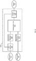
- Figure 4 is a block diagram illustrating an embodiment of a system for bypassing zero-result multiplications.
- system 400 is included in vector multiply unit 213 of Figure 2 .
- system 400 is a hardware multiplier system that is configured to bypass zero-result multiplications.
- a vector multiply unit e.g., vector multiply unit 213 of Figure 2 , includes a plurality of instances of system 400.
- system 400 receives operand A 402 and operand B 404 as inputs and produces result 416 as a final output.
- system 400 includes zero detector 406, operand A register 408, operand B register 410, multiplication unit 412, and output logic 414.
- operand A 402 and operand B 404 are integer or floating-point numbers. Examples of integer formats include 8-bit, 16-bit, 32-bit, signed, unsigned, etc. formats. Examples of floating-point formats include half-precision, single-precision, Brain Floating Point, etc.
- operand A 402 is to be multiplied with operand B 404 to obtain result 416.
- operand A register 408 stores operand A 402 and operand B register 410 stores operand B 404.
- operand A register 408 and operand B register B 410 are hardware registers (e.g., wherein each register comprises a plurality of flip-flop circuits), scratch memory locations, or another appropriate memory.
- Operand A register 408 and operand B register 410 are coupled to multiplication unit 412.
- Multiplication unit 412 is a hardware multiplier that produces a multiplication result based on inputs stored in operand A register 408 and operand B register 410.
- multiplication unit 412 is configured to handle integer multiplications (when operand A register 408 and operand B register 410 store numbers in an integer format).
- Multiplication unit 412 may also be configured to handle floating-point multiplications (when operand A register 408 and operand B register 410 store numbers in a floating-point format).
- operand A register 408 or operand B register 410 stores a zero value
- the multiplication result is necessarily a zero-value result (without needing to perform computation).
- new values of operand A 402 and operand B 404 are continually supplied to system 400 so that multiplication results are continually being produced.
- operand A register 408 and operand B register 410 are typically updated (loaded with the new operand values) to reflect the multiplication operation to be performed for that cycle.
- operand A register 408 and operand B register 410 do not need to be updated if at least one of the new operands during a new cycle has a zero value.
- operand A register 408 and operand B register 410 are not updated, which saves power due to not activating switching circuits (e.g., logic gates) used to update the registers. This reduces overall power consumption associated with using multiplication unit 412 to perform multiplication operations.
- zero detector 406 determines whether operand A 402 has a zero value.
- zero detector 406 is implemented, at least in part, using a digital comparator that detects whether operand A 402 is equal to zero.
- the digital comparator may be implemented using a plurality of digital bit-comparators, wherein each digital bit-comparator is implemented using digital logic gates.
- zero detector 406 in response to a detection of a zero value by zero detector 406, zero detector 406 sends a disable signal to operand A register 408 and operand B register 410 to cause updating of operand A register 408 and operand B register 410 to be disabled and another data signal to output logic 414 to cause result 416 to be a zero-value result.
- operand A 402 is examined to determine if it is a zero. It is also possible to examine operand B 404 by placing another zero detector in the data path between operand B 404 and operand B register 410. If operand B 404 is examined, operand A register 408 and operand B register 410 updating can be disabled in response to a detection that operand B 404 has a zero value. In many scenarios, it may be more efficient to examine only one of the operands if zeros are more frequent in one group of operands (e.g., activations in an activation matrix corresponding to operand A 402) than in another group of operands (e.g., weights in a weights matrix corresponding to operand B 404). In such a scenario, examining only one operand saves power by consuming power for only one zero detector.
- output logic 414 is communicatively connected to zero detector 406.
- output logic 414 in response to a signal from zero detector 406 that a zero is provided, causes result 416 to be a zero-value result, and in response to a signal from zero detector 406 that a zero is not being provided, output logic 414 causes result 416 to be a multiplication result that is the product of operand A 402 and operand B 404 as outputted by multiplication unit 412.
- output logic 414 includes a plurality of AND gates in which each AND gate's inputs are an output bit of multiplication unit 412 and a data signal from zero detector 406, wherein the data signal is low when a zero has been detected and high when no zero has been detected.
- result 416 has all zero bits when zero detector 406 detects operand A 402 to be zero and has the output bits of multiplication unit 412 when zero detector 406 does not detect operand A 402 to be zero. It is also possible to use other logic gate combinations and/or multiplexer designs instead of using AND gates.
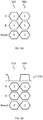
- Figures 5A and 5B are diagrams illustrating use of a data signal to control bypassing of a zero-result multiplication.
- Figures 5A and 5B illustrate how contents of operand and result storage (e.g., registers) differ when a system for bypassing zero-result multiplications is used.
- the example of Figure 5A shows multiplication of operands during two consecutive cycles 502 and 504 (e.g., two consecutive clock cycles) without using a system for bypassing zero-result multiplications.
- Operand A storage is loaded with the value 2
- operand B storage is loaded with the value 4
- the multiplication result of the two operands is 8.
- the operands are multiplied using a multiplication unit.
- Operand A storage is loaded with the value 0
- operand B storage is loaded with the value 5
- multiplication of the two operands is 0.
- the example of Figure 5B illustrates use of a data signal indicating detection of an operand value of zero.
- a system for bypassing zero-result multiplications is used.
- the system for bypassing zero-result multiplications is system 400 of Figure 4 .
- operands to be multiplied are operand A 402 and operand B 404 of Figure 4 .
- Zero detection signal 516 is a data signal indicating the detection of at least one zero operand during a cycle.
- zero detection signal 516 is produced by zero detector 406 of Figure 4 .
- none of the operands to be multiplied (2 and 4) have a zero value; thus, signal 516 is low during cycle 512.
- operand A storage is loaded with the value 2
- operand B storage is loaded with the value 4
- the multiplication result of the two operands is 8.
- operand A storage is operand A register 408 of Figure 4
- operand B storage is operand B register 410 of Figure 4
- the multiplication result is generated using multiplication unit 412 of Figure 4 .
- one of the operands to be multiplied (0 and 5) has a zero value; thus, signal 516 is high during cycle 514.
- this high signal causes operand A storage and operand B storage to not update their contents (in contrast to what is shown for cycle 504 of Figure 5A ).
- the contents of operand A storage and operand B storage have not updated.
- operand A storage still stores the value 2 from cycle 512 and operand B storage still stores the value 4 from cycle 512.
- the result of the multiplication is still the correct value of 0 (the same as for cycle 504 of Figure 5A ).
- zero detection signal 516 is received by output logic, which causes the final result of the multiplication to be zero when zero detection signal 516 is high.
- the output logic is output logic 414 of Figure 4 .
- a benefit of bypassing zero-result multiplications as shown in Figure 5B is reduced power consumption due to not updating operand storage (e.g., registers) as frequently but still obtaining correct multiplication results.
- Figure 6 is a flow chart illustrating an embodiment of a process for bypassing zero-result multiplications.
- the process of Figure 6 is performed by system 400 of Figure 4 .
- at least a portion of the process of Figure 6 is performed in 305 of Figure 3 .
- a zero value is provided.
- a single operand that is received is examined (e.g., operand A 402 of Figure 4 ). It is also possible to examine more than one operand (e.g., also examine operand B 404 of Figure 4 in addition to operand A 402) and determine if at least one of the operands has a zero value.
- zero detector 406 determines whether a zero value is provided.
- operand register values are updated.
- the operand registers are operand A register 408 and operand B register 410 of Figure 4 .
- the operand registers are loaded with the current operand values that are to be multiplied. Because no zero value has been provided, the output is not already known to be zero (or any other number, in general).
- the contents of the operand registers need to be updated and a multiplication unit needs to perform a multiplication to determine a multiplication result.
- a result of a multiplication unit is outputted.
- a result of multiplication unit 412 of Figure 4 is outputted.
- the multiplication by the multiplication unit needs to be performed because the multiplication result is not already known to be zero.
- output logic 414 of Figure 4 causes the result of multiplication unit 412 to be selected as a final result to be provided (e.g., result 416 of Figure 4 ) in response to the determination that no zero-value operand has been provided.
- updating of at least one operand register is disabled.
- updating of more than one operand register is disabled (e.g., updating of both operand A register 408 and operand B register 410 of Figure 4 is disabled).
- the one or more registers do not need to be updated because if it is determined that a zero value has been provided, then the result of the multiplication is already known to be zero without a need to load the registers and perform a multiplication using the contents of the updated registers.
- multiplexers and/or basic digital logic gates are used to implement disabling signals.
- a zero-value result is outputted.
- a multiplication result of a multiplication unit e.g., of multiplication unit 412 of Figure 4
- output logic 414 of Figure 4 outputs a zero-value result (e.g., to provide result 416 of Figure 4 ) in response to the determination that a zero-value operand has been provided.
Landscapes
- Engineering & Computer Science (AREA)
- Physics & Mathematics (AREA)
- General Physics & Mathematics (AREA)
- Theoretical Computer Science (AREA)
- Computational Mathematics (AREA)
- Mathematical Analysis (AREA)
- Mathematical Optimization (AREA)
- Pure & Applied Mathematics (AREA)
- Computing Systems (AREA)
- Mathematical Physics (AREA)
- General Engineering & Computer Science (AREA)
- Data Mining & Analysis (AREA)
- Software Systems (AREA)
- Algebra (AREA)
- Databases & Information Systems (AREA)
- Health & Medical Sciences (AREA)
- Life Sciences & Earth Sciences (AREA)
- Biomedical Technology (AREA)
- Biophysics (AREA)
- Nonlinear Science (AREA)
- Neurology (AREA)
- Computational Linguistics (AREA)
- Evolutionary Computation (AREA)
- General Health & Medical Sciences (AREA)
- Molecular Biology (AREA)
- Artificial Intelligence (AREA)
- Advance Control (AREA)
Abstract
Description
- A device for improving the efficiency of hardware multiplication operations is disclosed.
- A whole class of complex artificial intelligence problems can be solved using neural networks. One common operation required by many neural networks is a multiplication operation, for example, when performing matrix operations. Since artificial intelligence problems are often computationally and data intensive, hardware solutions are often beneficial for improving performance. It is a technical challenge to create a hardware platform that has high computational performance and low power consumption. Therefore, there exists a need for techniques directed toward energy efficient, high throughput matrix multiplication schemes that do not introduce significant hardware complexity and expense.
- In accordance with a first aspect of the present disclosure, there is provided a device, comprising: a first operand register configured to store a first operand value; a second operand register configured to store a second operand value; a multiplication unit configured to at least multiply the first operand value with the second operand value; and a hardware logic component configured to: detect whether a zero value is provided and in response to a detection that the zero value is being provided: cause an update of at least the first operand register to be disabled; and cause a result of a multiplication of the first operand value with the second operand value to be a zero-value result.
- In some embodiments, the first operand value and the second operand value may be in an integer number format.
- In some embodiments, the first operand value and the second operand value may be in a floating-point number format.
- In some embodiments, the multiplication unit may be further configured to receive a multiply operation instruction that specifies an operand format type.
- In some embodiments, the hardware logic component may include a comparator that is configured to detect whether the zero value is provided.
- In some embodiments, the hardware logic component may be configured to, in response to the detection that the zero value is being provided, cause the update of at least the first operand register to be disabled including by being configured to transmit a disable signal to the first operand register.
- In some embodiments, the hardware logic component may be further configured to, in response to the detection that the zero value is being provided, cause an update of the second operand register to be disabled.
- In some embodiments, the hardware logic component may be configured to, in response to the detection that the zero value is being provided, cause the update of the first operand register and the update of the second operand register to be disabled including by being configured to transmit disable signals to both the first operand register and the second operand register.
- In some embodiments, the hardware logic component may be configured to, in response to the detection that the zero value is being provided, cause the result of the multiplication of the first operand value with the second operand value to be the zero-value result including by being configured to transmit a signal indicating the detection that the zero value is being provided to an output logic component.
- In some embodiments, the output logic component may be configured to select between an output of the multiplication unit and the zero-value result.
- In some embodiments, the output logic component may be configured to select the zero-value result in response to the detection that the zero value is being provided.
- In some embodiments, the output logic component may be configured to select the output of the multiplication unit in response to a detection by the hardware logic component that a non-zero value is being provided.
- In some embodiments, the output logic component may include an AND digital logic gate.
- In some embodiments, the output logic component may include a multiplexer.
- In some embodiments, the multiplication of the first operand value with the second operand value may be a part of a plurality of multiplications associated with a vector multiplication or a dot product operation.
- In some embodiments, the multiplication of the first operand value with the second operand value may be a part of a matrix operation.
- In some embodiments, the multiplication of the first operand value with the second operand value may be a part of an artificial neural network operation.
- In some embodiments, the result of the multiplication of the first operand value with the second operand value may be an input to a hardware adder.
- In accordance with a second aspect of the present disclosure, there is provided a method, comprising: receiving a first operand value that is to be stored in a first operand register; receiving a second operand value that is to be stored in a second operand register, wherein the first operand value and the second operand value are to be multiplied by a multiplication unit; detecting whether a zero value is provided; and in response to a detection that the zero value is being provided: causing an update of at least the first operand register to be disabled; and causing a result of a multiplication of the first operand value with the second operand value to be a zero-value result.
- In accordance with a third aspect of the present disclosure, there is provided an integrated circuit processor, comprising: a first operand register configured to store a first operand value; a second operand register configured to store a second operand value; a multiplication unit configured to at least multiply the first operand value with the second operand value; a first hardware logic component configured to: detect whether a first zero value is provided and in response to a detection that the first zero value is being provided: cause an update of at least the first operand register to be disabled; and cause a result of a multiplication of the first operand value with the second operand value to be a zero-value result; and a second hardware logic component configured to: detect whether a second zero value is provided and in response to a detection that the second zero value is being provided: cause an update of at least the second operand register to be disabled; and cause the result of the multiplication of the first operand value with the second operand value to be the zero-value result.
- It will be appreciated that any features described herein as being suitable for incorporation into one or more aspects or embodiments of the present invention are intended to be generalizable across any and all aspects and embodiments of the present disclosure. Other aspects of the present disclosure can be understood by those skilled in the art in light of the description, the claims, and the drawings of the present disclosure. The foregoing general description and the following detailed description are exemplary and explanatory only and are not restrictive of the claims.
- Various embodiments of the invention are disclosed in the following detailed description and the accompanying drawings.
-
Figure 1 is a block diagram illustrating an embodiment of a system for solving artificial intelligence problems using a neural network. -
Figure 2 is a block diagram illustrating an embodiment of a processing element for solving artificial intelligence problems using a neural network. -
Figure 3 is a flow chart illustrating an embodiment of a process for performing a multiplication in hardware. -
Figure 4 is a block diagram illustrating an embodiment of a system for bypassing zero-result multiplications. -
Figures 5A and 5B are diagrams illustrating use of a data signal to control bypassing of a zero-result multiplication. -
Figure 6 is a flow chart illustrating an embodiment of a process for bypassing zero-result multiplications. - The invention can be implemented in numerous ways, including as a process; an apparatus; a system; a composition of matter; a computer program product embodied on a computer readable storage medium; and/or a processor, such as a processor configured to execute instructions stored on and/or provided by a memory coupled to the processor. In this specification, these implementations, or any other form that the invention may take, may be referred to as techniques. In general, the order of the steps of disclosed processes may be altered within the scope of the invention. Unless stated otherwise, a component such as a processor or a memory described as being configured to perform a task may be implemented as a general component that is temporarily configured to perform the task at a given time or a specific component that is manufactured to perform the task. As used herein, the term 'processor' refers to one or more devices, circuits, and/or processing cores configured to process data, such as computer program instructions.
- A detailed description of one or more embodiments of the invention is provided below along with accompanying figures that illustrate the principles of the invention. The invention is described in connection with such embodiments, but the invention is not limited to any embodiment. The scope of the invention is limited only by the claims and the invention encompasses numerous alternatives, modifications and equivalents. Numerous specific details are set forth in the following description in order to provide a thorough understanding of the invention. These details are provided for the purpose of example and the invention may be practiced according to the claims without some or all of these specific details. For the purpose of clarity, technical material that is known in the technical fields related to the invention has not been described in detail so that the invention is not unnecessarily obscured.
- A device for improving the efficiency of hardware multiplication operations is disclosed. The disclosed device includes a first operand register configured to store a first operand value, a second operand register configured to store a second operand value, a multiplication unit configured to at least multiply the first operand value with the second operand value, and a hardware logic component configured to: detect whether a zero value is provided and, in response to a detection that the zero value is being provided, cause an update of at least the first operand register to be disabled and cause a result of a multiplication of the first operand value with the second operand value to be a zero-value result. Practical and technological benefits of the disclosed device include improved efficiency and performance of multiplication operations, e.g., by not wasting power on performing multiplications that are zero-result multiplications.
- A common component in many neural networks is a fast, efficient hardware matrix multiplier. Typically, the matrix multiplier is a large contributor to overall power consumption of an integrated circuit on which neural network hardware is implemented. Because many neural networks receive a large fraction of zeros in the activations (as well as some zero weights), many multiplications do not need to be fully performed. The disclosed techniques can reduce the power consumption of the hardware matrix multiplier by bypassing multiplications in which at least one input (of a multiplication) is zero. If at least one input is zero, then the result of the multiplication can be determined to be zero without performing any computation.
- In various embodiments, a hardware matrix multiplier includes a plurality of dot product modules, each of which computes a dot product of a row of a first input matrix (A) with a column of a second matrix (B). In some embodiments, each dot product module includes a layer of input registers (that store elements of A and B) and are coupled to a series of hardware multipliers (also referred to herein as multipliers and multiplication units) that are connected to an adder tree. In each cycle, a new column of B may be loaded, which may then be broadcasted to all of the dot product modules in order to determine dot products with all rows of A in parallel. In a hardware multiplier that does not bypass zero-value results, if a new element of B is zero, then a multiplication occurs (as it would if the new element of B were a nonzero value). Power is consumed due to logic gates switching even though the final result of the multiplication is already known to be zero.
- In various embodiments, wasting of power via switching of logic gates in a multiplication that is already known to have a zero-value result is avoided by making specified modifications to hardware multipliers. In various embodiments, before storing new elements of A and/or B in input registers, it is determined whether one of the elements is zero. In some embodiments, only one of the elements is examined to determine if it is a zero, which may be more efficient because zeros can be more frequent in one matrix than in the other (e.g., more frequent in activations than in weights). In response to a detection that a zero value is being provided, a signal can be sent to cause the input registers to not be updated, which avoids wasting power switching the logic gates of the registers. In some embodiments, a multiplexer or a flip-flop with an enable or disable signal is used to indicate whether input registers should be updated. In various embodiments, an "is zero" signal is set to high if a newly loaded element is zero and. The "is zero" signal can be routed to output logic of a hardware multiplier. A high value of the "is zero" signal causes the current output of the hardware multiplier to not be used as the final result (the current output of the hardware multiplier would be the output that was computed with the previous element of B because input registers would not have been updated). Instead, a zero value is used as the final result. Example implementations of such output logic are described in further detail below.
-
Figure 1 is a block diagram illustrating an embodiment of a system for solving artificial intelligence problems using a neural network. For example,system 100 may be applied to use a neural network to solve problems such as image recognition and recommendation system matches. In the example shown,system 100 includes multiple processing elements such asprocessing elements bus 151.System 100 may include fewer or more processing elements. For example, the number of processing elements can be scaled up or down depending on the intended computational and data requirements. In some embodiments, the processing elements, such as 101, 111, and 121, are communicatively connected to one another and/or memory unit 131 viabus 151. For example, the memory unit may be a last level cache (LLC) and/or may be implemented using static random-access memory (SRAM). Each processing element may be utilized bysystem 100 to perform matrix compute operations such as matrix multiplications including integer and floating-point multiplications. - In some embodiments, a communication bus, such as
bus 151, is used to transmit processing element instructions and optional instruction arguments. For example, a matrix operation and matrix operands may be transmitted to a processing element, such asprocessing elements bus 151. Additional processing element instructions may include multiplication operation instructions such as integer or floating-point multiplication operation instructions. In various embodiments, a large, complex artificial intelligence problem can be solved usingsystem 100 by subdividing the problem into smaller sub-problems. The smaller sub-problems can be assigned and distributed to different processing elements. The results of the smaller sub-problems can be merged to determine the solution to the larger and more complex problem. In some scenarios, the sub-problems are solved in parallel and/or in pipelined stages. In some scenarios, the result from a first processing element is fed as an input to a second processing element. - In some embodiments, each processing element of
system 100 includes at least a control logic unit and a matrix compute engine. As shown with respect toprocessing element 111,processing element 111 includescontrol logic 113 andmatrix compute engine 115.Processing elements elements control logic 113 processes instructions directed toprocessing element 111 viacommunication bus 151. For example, a processing element instruction may include an integer or floating-point multiplication instruction. In some embodiments,control logic 113 determines how to perform the integer or floating-point multiplication usingmatrix compute engine 115, including how to determine components of integer or floating-point number operands. In some embodiments,control logic 113 receives processing element instructions viabus 151 and can be used to initiate retrieving and/or writing data from/to memory 131. - In some embodiments,
matrix compute engine 115 is a hardware matrix compute engine for performing matrix operations including operations related to integer multiplication, floating-point multiplication, matrix multiplication, and/or convolution operations. For example,matrix compute engine 115 may be a matrix engine for performing dot product operations requiring integer or floating-point multiplications and addition operations. In some embodiments, the convolution operations supported include depthwise, groupwise, normal, regular, pointwise, two-dimensional, and/or three-dimensional convolutions, among others. For example,matrix compute engine 115 may receive a first input matrix such as a subset of a large image and a second input matrix such as a filter, kernel, or convolution matrix, etc. to apply to the first input matrix.Matrix compute engine 115 can be used to perform a convolution operation using the two input matrices to determine a resulting output matrix. In some embodiments,matrix compute engine 115 includes input and/or output buffers for loading input data matrices or vectors and writing out a result data matrix or vector. In some embodiments,matrix compute engine 115 includes multiple vector units and each vector unit includes a vector multiply unit and a vector adder unit. -
Figure 2 is a block diagram illustrating an embodiment of a processing element for solving artificial intelligence problems using a neural network. In the example shown,processing element 201 is communicatively connected tobus 251.Processing element 201 includescontrol logic 203 andmatrix compute engine 205.Matrix compute engine 205 includesvector units Matrix compute engine 205 may include more or fewer vector units. For example, a matrix compute engine may include 32 vector units, each capable of processing two 32-element vectors. In various embodiments, each vector unit includes a vector multiply unit and a vector adder unit. In the example shown,vector unit 211 includes vector multiplyunit 213 andvector adder unit 215. For simplicity, the vector multiply and vector adder units ofvector units unit 213 andvector adder unit 215. In some embodiments,processing element 201 is processingelement Figure 1 . In some embodiments,control logic 203 andmatrix compute engine 205 are, respectively,control logic 113 andmatrix compute engine 115 ofFigure 1 . - In some embodiments,
matrix compute engine 205 receives input matrix (or vector) operands to perform matrix operations. For example,matrix compute engine 205 may receive one or more data input vectors corresponding to a portion of an image and at least one weight input vector corresponding to a filter matrix. The input vectors, such as input data and weight vectors, may be passed as arguments to a vector unit, such as one ofvector units matrix compute engine 205. For example, a vector unit ofmatrix compute engine 205 may determine a matrix result, such as a dot product result, using a data input vector and weight input vector pair. In some embodiments,matrix compute engine 205 includes 32 vector units. Each vector unit may take two 32-element vectors as arguments and each determine a 32-element vector result. In some embodiments, the result is a single element result and taken across all vector units ofmatrix compute engine 205. In some embodiments, the result is an output vector result. In various embodiments, output results are determined by accumulating partial vector results across multiple vector unit operations. For example, a multiplication operation can be decomposed into multiple multiplication operations and the results summed. The number of vector units ofmatrix compute engine 205 can vary as can the vector unit lengths and element sizes. For example, elements may be 4-bit, 8-bit, 16-bit, 1-byte, 2-byte, 4-byte, or another appropriate size. Depending on the capabilities of the vector unit, different element sizes can be natively supported. - In some embodiments, each vector unit of
matrix compute engine 205, such asvector units - In some embodiments, each vector unit of
matrix compute engine 205, such asvector units unit 213, is configured to multiply corresponding elements received via input vector operands. In some embodiments, the result is a vector of multiplication results. For example, for two 32-bit input vectors, the result of a vector multiply unit is a vector of 32-bit multiplication results. The first element from a first input vector is multiplied with the first element of a second input vector. Similarly, the second element from the first input vector is multiplied with the second element of the second input vector. In various embodiments, the vector of multiplication results is passed to a vector adder unit of the vector unit. For example, vector multiplyunit 213 can pass its multiplication results tovector adder unit 215.Vector adder unit 215 can be used for addition operations such as summing partial results, computing at least in part a dot product result, or other appropriate functionality. - In some embodiments, each vector adder unit of a vector unit, such as
vector adder unit 215, is configured to compute addition operations using elements from an input vector. For example, the sum of selected elements from a vector of multiplication results computed by vector multiplyunit 213 is computed byvector adder unit 215. In some embodiments, the result of a vector adder unit is a dot product of the vectors used as inputs to the corresponding vector multiply unit. In various embodiments, each vector adder unit, such asvector adder unit 215, is implemented as an adder tree. For example, the top level of an adder tree may add pairs of elements to determine a set of partial sums, such as addingelements 0 and 1 to determine a first partial sum andelements 2 and 3 to determine a second partial sum, etc. Each subsequent level may sum pairs of partial sums from the previous level until the last level computes a final result sum. In some embodiments, specified partial sums may be outputted as a result of the adder unit. In various embodiments, each adder tree computes partial sums in parallel to arrive at a result sum. The parallel operation significantly improves the efficiency of summing a vector of numbers. In various embodiments, multiple vector units can operate in parallel to compute multiple results in parallel, significantly improving the throughput ofmatrix compute engine 205. - In some embodiments,
matrix compute engine 205 includes one or more accumulators, for example, to accumulate the results of each vector unit. In some embodiments, an accumulator is included as part of a vector unit or as part ofmatrix compute engine 205 as appropriate. The accumulator(s) can be used to sum the results computed across multiple iterations of the vector units. For example, the result from one iteration of a vector unit can be stored in an accumulator and added to the result of the next iteration of the vector unit. In some embodiments, the accumulator is a vector accumulator. For example, the accumulator may be sized based on the size of an output vector ofmatrix compute engine 205. In various embodiments, once matrix processing is complete, the accumulator results are pushed to memory viabus 251. -
Figure 3 is a flow chart illustrating an embodiment of a process for performing a multiplication in hardware. In the process ofFigure 3 , an integer or floating-point multiplication operation using multiplication operands of various formats may be performed. In various embodiments, a processing element handles multiple integer or floating-point number formats. In some embodiments, the process ofFigure 3 is performed in response to receiving a multiply operation instruction at a control unit of a processing element, such asprocessing elements Figure 1 and/orprocessing element 201 ofFigure 2 . - At 301, a multiply processor instruction is received. The multiply operation instruction may specify two integer or floating-point numbers. In some embodiments, the instruction is a vector instruction. For example, two vectors of operands may be received and each element of a first vector is to be multiplied with a corresponding element of a second vector.
- At 303, the operand formats are identified. In various embodiments, multiple different integer and floating-point formats are supported by the processing element. In some embodiments, format is specified by the multiply processor instruction. For example, a flag in the multiply processor instruction can identify a type of integer format or a type of floating-point format.
- At 305, a multiplication is performed. For example, a multiplication of two integer or floating-point numbers is performed. As another example, a multiplication of two vectors of integers or floating-point numbers can also be performed.
- At 307, the multiplication result(s) are provided. For example, result(s) can be provided to the next step for solving an artificial intelligence problem. In some embodiments, the result(s) are utilized to solve the next layer of a neural network and/or combined with results from other processing elements. In some embodiments, the result(s) are written back to memory such as memory 131 of
Figure 1 where the result(s) can be utilized by a subsequent operation. -
Figure 4 is a block diagram illustrating an embodiment of a system for bypassing zero-result multiplications. In some embodiments,system 400 is included in vector multiplyunit 213 ofFigure 2 . In various embodiments,system 400 is a hardware multiplier system that is configured to bypass zero-result multiplications. In various embodiments, a vector multiply unit, e.g., vector multiplyunit 213 ofFigure 2 , includes a plurality of instances ofsystem 400. - In the example shown,
system 400 receivesoperand A 402 andoperand B 404 as inputs and produces result 416 as a final output. In the example shown,system 400 includes zerodetector 406, operand Aregister 408,operand B register 410,multiplication unit 412, andoutput logic 414. In various embodiments,operand A 402 andoperand B 404 are integer or floating-point numbers. Examples of integer formats include 8-bit, 16-bit, 32-bit, signed, unsigned, etc. formats. Examples of floating-point formats include half-precision, single-precision, Brain Floating Point, etc. In various embodiments,operand A 402 is to be multiplied withoperand B 404 to obtainresult 416. - In the example shown, operand A
register 408 stores operand A 402 and operand B register 410stores operand B 404. In various embodiments, operand Aregister 408 and operandB register B 410 are hardware registers (e.g., wherein each register comprises a plurality of flip-flop circuits), scratch memory locations, or another appropriate memory. Operand Aregister 408 andoperand B register 410 are coupled tomultiplication unit 412.Multiplication unit 412 is a hardware multiplier that produces a multiplication result based on inputs stored in operand Aregister 408 andoperand B register 410. In some embodiments,multiplication unit 412 is configured to handle integer multiplications (when operand Aregister 408 andoperand B register 410 store numbers in an integer format).Multiplication unit 412 may also be configured to handle floating-point multiplications (when operand Aregister 408 andoperand B register 410 store numbers in a floating-point format). - If at least one of operand A
register 408 or operand B register 410 stores a zero value, the multiplication result is necessarily a zero-value result (without needing to perform computation). In various embodiments, new values ofoperand A 402 andoperand B 404 are continually supplied tosystem 400 so that multiplication results are continually being produced. On each cycle (e.g., a clock cycle whensystem 400 performs one multiplication per clock cycle), operand Aregister 408 andoperand B register 410 are typically updated (loaded with the new operand values) to reflect the multiplication operation to be performed for that cycle. However, operand Aregister 408 andoperand B register 410 do not need to be updated if at least one of the new operands during a new cycle has a zero value. Stated alternatively, if at least one zero input tomultiplication unit 412 is detected, operand Aregister 408 andoperand B register 410 are not updated, which saves power due to not activating switching circuits (e.g., logic gates) used to update the registers. This reduces overall power consumption associated with usingmultiplication unit 412 to perform multiplication operations. - In the example shown, zero
detector 406 determines whether operand A 402 has a zero value. In some embodiments, zerodetector 406 is implemented, at least in part, using a digital comparator that detects whether operand A 402 is equal to zero. The digital comparator may be implemented using a plurality of digital bit-comparators, wherein each digital bit-comparator is implemented using digital logic gates. In various embodiments, in response to a detection of a zero value by zerodetector 406, zerodetector 406 sends a disable signal to operand Aregister 408 andoperand B register 410 to cause updating of operand Aregister 408 andoperand B register 410 to be disabled and another data signal tooutput logic 414 to causeresult 416 to be a zero-value result. In the example shown, only operand A 402 is examined to determine if it is a zero. It is also possible to examineoperand B 404 by placing another zero detector in the data path betweenoperand B 404 andoperand B register 410. Ifoperand B 404 is examined, operand Aregister 408 andoperand B register 410 updating can be disabled in response to a detection that operandB 404 has a zero value. In many scenarios, it may be more efficient to examine only one of the operands if zeros are more frequent in one group of operands (e.g., activations in an activation matrix corresponding to operand A 402) than in another group of operands (e.g., weights in a weights matrix corresponding to operand B 404). In such a scenario, examining only one operand saves power by consuming power for only one zero detector. - In the example shown,
output logic 414 is communicatively connected to zerodetector 406. In various embodiments, in response to a signal from zerodetector 406 that a zero is provided,output logic 414 causes result 416 to be a zero-value result, and in response to a signal from zerodetector 406 that a zero is not being provided,output logic 414 causes result 416 to be a multiplication result that is the product ofoperand A 402 andoperand B 404 as outputted bymultiplication unit 412. In some embodiments,output logic 414 includes a plurality of AND gates in which each AND gate's inputs are an output bit ofmultiplication unit 412 and a data signal from zerodetector 406, wherein the data signal is low when a zero has been detected and high when no zero has been detected. Thus, result 416 has all zero bits when zerodetector 406 detectsoperand A 402 to be zero and has the output bits ofmultiplication unit 412 when zerodetector 406 does not detectoperand A 402 to be zero. It is also possible to use other logic gate combinations and/or multiplexer designs instead of using AND gates. - In the example illustrated in
Figure 4 , portions of the communication path between the components are shown. Other communication paths may exist, and the example ofFigure 4 has been simplified to illustrate the example clearly. For example, signals from zerodetector 406 that disable the updating of registers are not shown explicitly. In various embodiments, zerodetector 406 is communicatively connected to both operand Aregister 408 andoperand B register 410 so that a disable signal can be sent to both registers. Although single instances of components have been shown to simplify the diagram, additional instances of any of the components shown inFigure 4 may exist. The number of components and the connections shown inFigure 4 are merely illustrative. Components not shown inFigure 4 may also exist. -
Figures 5A and 5B are diagrams illustrating use of a data signal to control bypassing of a zero-result multiplication.Figures 5A and 5B illustrate how contents of operand and result storage (e.g., registers) differ when a system for bypassing zero-result multiplications is used. The example ofFigure 5A shows multiplication of operands during twoconsecutive cycles 502 and 504 (e.g., two consecutive clock cycles) without using a system for bypassing zero-result multiplications. Duringcycle 502, the multiplication to be performed is 2 x 4 = 8. Operand A storage is loaded with thevalue 2, operand B storage is loaded with thevalue 4, and the multiplication result of the two operands is 8. In various embodiments, the operands are multiplied using a multiplication unit. Duringcycle 504, the multiplication to be performed is 0 x 5 = 0. Operand A storage is loaded with thevalue 0, operand B storage is loaded with thevalue 5, and multiplication of the two operands is 0. - The example of
Figure 5B illustrates use of a data signal indicating detection of an operand value of zero. In the example ofFigure 5B , a system for bypassing zero-result multiplications is used. In some embodiments, the system for bypassing zero-result multiplications issystem 400 ofFigure 4 . In some embodiments, operands to be multiplied areoperand A 402 andoperand B 404 ofFigure 4 . In the example ofFigure 5B , duringconsecutive cycles 512 and 514 (e.g., two consecutive clock cycles), the multiplications that are to be performed are the same as duringcycles Figure 5A (2 x 4 = 8 and then 0 x 5 = 0). Zerodetection signal 516 is a data signal indicating the detection of at least one zero operand during a cycle. In some embodiments, zerodetection signal 516 is produced by zerodetector 406 ofFigure 4 . Duringcycle 512, none of the operands to be multiplied (2 and 4) have a zero value; thus, signal 516 is low duringcycle 512. As withcycle 502 ofFigure 5A , duringcycle 512, operand A storage is loaded with thevalue 2, operand B storage is loaded with thevalue 4, and the multiplication result of the two operands is 8. In some embodiments, operand A storage is operand Aregister 408 ofFigure 4 , operand B storage is operand B register 410 ofFigure 4 , and the multiplication result is generated usingmultiplication unit 412 ofFigure 4 . - During
cycle 514, one of the operands to be multiplied (0 and 5) has a zero value; thus, signal 516 is high duringcycle 514. In various embodiments, this high signal causes operand A storage and operand B storage to not update their contents (in contrast to what is shown forcycle 504 ofFigure 5A ). In the example shown, duringcycle 514, the contents of operand A storage and operand B storage have not updated. Stated alternatively, in the example shown, duringcycle 514, operand A storage still stores thevalue 2 fromcycle 512 and operand B storage still stores thevalue 4 fromcycle 512. However, the result of the multiplication is still the correct value of 0 (the same as forcycle 504 ofFigure 5A ). In various embodiments, zerodetection signal 516 is received by output logic, which causes the final result of the multiplication to be zero when zerodetection signal 516 is high. In some embodiments, the output logic isoutput logic 414 ofFigure 4 . A benefit of bypassing zero-result multiplications as shown inFigure 5B is reduced power consumption due to not updating operand storage (e.g., registers) as frequently but still obtaining correct multiplication results. -
Figure 6 is a flow chart illustrating an embodiment of a process for bypassing zero-result multiplications. In some embodiments, the process ofFigure 6 is performed bysystem 400 ofFigure 4 . In some embodiments, at least a portion of the process ofFigure 6 is performed in 305 ofFigure 3 . - At 602, it is determined whether a zero value is provided. In some embodiments, a single operand that is received is examined (e.g.,
operand A 402 ofFigure 4 ). It is also possible to examine more than one operand (e.g., also examineoperand B 404 ofFigure 4 in addition to operand A 402) and determine if at least one of the operands has a zero value. In some embodiments, zerodetector 406 determines whether a zero value is provided. - If at 602 it is determined that no zero value has been provided, at 604, operand register values are updated. In some embodiments, the operand registers are operand A
register 408 and operand B register 410 ofFigure 4 . The operand registers are loaded with the current operand values that are to be multiplied. Because no zero value has been provided, the output is not already known to be zero (or any other number, in general). The contents of the operand registers need to be updated and a multiplication unit needs to perform a multiplication to determine a multiplication result. - At 606, a result of a multiplication unit is outputted. In some embodiments, a result of
multiplication unit 412 ofFigure 4 is outputted. The multiplication by the multiplication unit needs to be performed because the multiplication result is not already known to be zero. In some embodiments,output logic 414 ofFigure 4 causes the result ofmultiplication unit 412 to be selected as a final result to be provided (e.g., result 416 ofFigure 4 ) in response to the determination that no zero-value operand has been provided. - If at 602, it is determined that a zero value has been provided, at 608, updating of at least one operand register is disabled. In various embodiments, updating of more than one operand register is disabled (e.g., updating of both operand A
register 408 and operand B register 410 ofFigure 4 is disabled). The one or more registers do not need to be updated because if it is determined that a zero value has been provided, then the result of the multiplication is already known to be zero without a need to load the registers and perform a multiplication using the contents of the updated registers. In some embodiments, multiplexers and/or basic digital logic gates are used to implement disabling signals. - At 610, a zero-value result is outputted. A multiplication result of a multiplication unit (e.g., of
multiplication unit 412 ofFigure 4 ) is not needed because the multiplication result is already known to be zero. In some embodiments,output logic 414 ofFigure 4 outputs a zero-value result (e.g., to provideresult 416 ofFigure 4 ) in response to the determination that a zero-value operand has been provided. - Although the foregoing embodiments have been described in some detail for purposes of clarity of understanding, the invention is not limited to the details provided. There are many alternative ways of implementing the invention. The disclosed embodiments are illustrative and not restrictive.
Claims (14)
- A device, comprising:a first operand register configured to store a first operand value;a second operand register configured to store a second operand value;a multiplication unit configured to at least multiply the first operand value with the second operand value; anda hardware logic component configured to:
detect whether a zero value is provided and in response to a detection that the zero value is being provided:cause an update of at least the first operand register to be disabled; andcause a result of a multiplication of the first operand value with the second operand value to be a zero-value result. - The device of claim 1, wherein the first operand value and the second operand value are in an integer number format; or preferably wherein the first operand value and the second operand value are in a floating-point number format.
- The device of claim 1 or claim 2, wherein the multiplication unit is further configured to receive a multiply operation instruction that specifies an operand format type.
- The device of any one of claims 1 to 3, wherein the hardware logic component includes a comparator that is configured to detect whether the zero value is provided.
- The device of any one of the preceding claims, wherein the hardware logic component is configured to, in response to the detection that the zero value is being provided, cause the update of at least the first operand register to be disabled including by being configured to transmit a disable signal to the first operand register.
- The device of any one of the preceding claims, wherein the hardware logic component is further configured to, in response to the detection that the zero value is being provided, cause an update of the second operand register to be disabled; and preferably wherein the hardware logic component is configured to, in response to the detection that the zero value is being provided, cause the update of the first operand register and the update of the second operand register to be disabled including by being configured to transmit disable signals to both the first operand register and the second operand register.
- The device of any one of the preceding claims, wherein the hardware logic component is configured to, in response to the detection that the zero value is being provided, cause the result of the multiplication of the first operand value with the second operand value to be the zero-value result including by being configured to transmit a signal indicating the detection that the zero value is being provided to an output logic component.
- The device of claim 7, wherein the output logic component is configured to select between an output of the multiplication unit and the zero-value result; and preferably:i. wherein the output logic component is configured to select the zero-value result in response to the detection that the zero value is being provided; and preferably wherein the output logic component is configured to select the output of the multiplication unit in response to a detection by the hardware logic component that a non-zero value is being provided; and/orii. wherein the output logic component includes an AND digital logic gate; and/oriii. wherein the output logic component includes a multiplexer.
- The device of any one of the preceding claims, wherein the multiplication of the first operand value with the second operand value is a part of a plurality of multiplications associated with a vector multiplication or a dot product operation.
- The device of any one of the preceding claims, wherein the multiplication of the first operand value with the second operand value is a part of a matrix operation.
- The device of any one of the preceding claims, wherein the multiplication of the first operand value with the second operand value is a part of an artificial neural network operation.
- The device of any one of the preceding claims, wherein the result of the multiplication of the first operand value with the second operand value is an input to a hardware adder.
- A method, comprising:receiving a first operand value that is to be stored in a first operand register;receiving a second operand value that is to be stored in a second operand register, wherein the first operand value and the second operand value are to be multiplied by a multiplication unit;detecting whether a zero value is provided; andin response to a detection that the zero value is being provided:causing an update of at least the first operand register to be disabled; andcausing a result of a multiplication of the first operand value with the second operand value to be a zero-value result.
- An integrated circuit processor, comprising:a first operand register configured to store a first operand value;a second operand register configured to store a second operand value;a multiplication unit configured to at least multiply the first operand value with the second operand value;a first hardware logic component configured to:detect whether a first zero value is provided and in response to a detection that the first zero value is being provided:cause an update of at least the first operand register to be disabled; andcause a result of a multiplication of the first operand value with the secondoperand value to be a zero-value result; anda second hardware logic component configured to:
detect whether a second zero value is provided and in response to a detection that the second zero value is being provided:cause an update of at least the second operand register to be disabled; andcause the result of the multiplication of the first operand value with the second operand value to be the zero-value result.
Applications Claiming Priority (1)
| Application Number | Priority Date | Filing Date | Title |
|---|---|---|---|
| US16/869,288 US11614920B2 (en) | 2020-05-07 | 2020-05-07 | Bypassing zero-value multiplications in a hardware multiplier |
Publications (1)
| Publication Number | Publication Date |
|---|---|
| EP3907605A1 true EP3907605A1 (en) | 2021-11-10 |
Family
ID=75438616
Family Applications (1)
| Application Number | Title | Priority Date | Filing Date |
|---|---|---|---|
| EP21167381.9A Withdrawn EP3907605A1 (en) | 2020-05-07 | 2021-04-08 | Bypassing zero-value multiplications in a hardware multiplier |
Country Status (3)
| Country | Link |
|---|---|
| US (1) | US11614920B2 (en) |
| EP (1) | EP3907605A1 (en) |
| CN (1) | CN113626761A (en) |
Families Citing this family (2)
| Publication number | Priority date | Publication date | Assignee | Title |
|---|---|---|---|---|
| CN112835551B (en) * | 2021-03-09 | 2022-06-28 | 上海壁仞智能科技有限公司 | Data processing method, electronic device and computer readable storage medium for processing unit |
| US20240419402A1 (en) * | 2023-06-14 | 2024-12-19 | Microsoft Technology Licensing, Llc | Zero-detection for logic circuit multiplication |
Citations (6)
| Publication number | Priority date | Publication date | Assignee | Title |
|---|---|---|---|---|
| US20120117441A1 (en) * | 1998-08-24 | 2012-05-10 | Microunity Systems Engineering, Inc. | Processor Architecture for Executing Wide Transform Slice Instructions |
| US20180173527A1 (en) * | 2016-12-15 | 2018-06-21 | Optimum Semiconductor Technologies, Inc. | Floating point instruction format with embedded rounding rule |
| US20180322390A1 (en) * | 2017-05-05 | 2018-11-08 | Intel Corporation | Optimized compute hardware for machine learning operations |
| US20190042250A1 (en) * | 2018-06-08 | 2019-02-07 | Intel Corporation | Variable format, variable sparsity matrix multiplication instruction |
| US20190065150A1 (en) * | 2017-08-31 | 2019-02-28 | Qualcomm Incorporated | Providing efficient multiplication of sparse matrices in matrix-processor-based devices |
| US20190205746A1 (en) * | 2017-12-29 | 2019-07-04 | Intel Corporation | Machine learning sparse computation mechanism for arbitrary neural networks, arithmetic compute microarchitecture, and sparsity for training mechanism |
Family Cites Families (10)
| Publication number | Priority date | Publication date | Assignee | Title |
|---|---|---|---|---|
| US7539714B2 (en) * | 2003-06-30 | 2009-05-26 | Intel Corporation | Method, apparatus, and instruction for performing a sign operation that multiplies |
| US7631207B1 (en) * | 2006-04-21 | 2009-12-08 | Sun Microsystems, Inc. | Reducing power consumption for processing of common values in microprocessor registers and execution units |
| US8660380B2 (en) * | 2006-08-25 | 2014-02-25 | Nvidia Corporation | Method and system for performing two-dimensional transform on data value array with reduced power consumption |
| US8577948B2 (en) * | 2010-09-20 | 2013-11-05 | Intel Corporation | Split path multiply accumulate unit |
| US9116634B2 (en) * | 2011-06-10 | 2015-08-25 | International Business Machines Corporation | Configure storage class memory command |
| US9213523B2 (en) * | 2012-06-29 | 2015-12-15 | Intel Corporation | Double rounded combined floating-point multiply and add |
| JP2015012412A (en) * | 2013-06-28 | 2015-01-19 | 富士通株式会社 | Distortion compensation apparatus, distortion compensation method, and wireless communication apparatus |
| US20180164866A1 (en) * | 2016-12-13 | 2018-06-14 | Qualcomm Incorporated | Low-power architecture for sparse neural network |
| US10817260B1 (en) * | 2018-06-13 | 2020-10-27 | Amazon Technologies, Inc. | Reducing dynamic power consumption in arrays |
| US10901492B1 (en) * | 2019-03-29 | 2021-01-26 | Amazon Technologies, Inc. | Power reduction in processor pipeline by detecting zeros |
-
2020
- 2020-05-07 US US16/869,288 patent/US11614920B2/en active Active
-
2021
- 2021-04-08 EP EP21167381.9A patent/EP3907605A1/en not_active Withdrawn
- 2021-05-07 CN CN202110496149.3A patent/CN113626761A/en active Pending
Patent Citations (6)
| Publication number | Priority date | Publication date | Assignee | Title |
|---|---|---|---|---|
| US20120117441A1 (en) * | 1998-08-24 | 2012-05-10 | Microunity Systems Engineering, Inc. | Processor Architecture for Executing Wide Transform Slice Instructions |
| US20180173527A1 (en) * | 2016-12-15 | 2018-06-21 | Optimum Semiconductor Technologies, Inc. | Floating point instruction format with embedded rounding rule |
| US20180322390A1 (en) * | 2017-05-05 | 2018-11-08 | Intel Corporation | Optimized compute hardware for machine learning operations |
| US20190065150A1 (en) * | 2017-08-31 | 2019-02-28 | Qualcomm Incorporated | Providing efficient multiplication of sparse matrices in matrix-processor-based devices |
| US20190205746A1 (en) * | 2017-12-29 | 2019-07-04 | Intel Corporation | Machine learning sparse computation mechanism for arbitrary neural networks, arithmetic compute microarchitecture, and sparsity for training mechanism |
| US20190042250A1 (en) * | 2018-06-08 | 2019-02-07 | Intel Corporation | Variable format, variable sparsity matrix multiplication instruction |
Non-Patent Citations (1)
| Title |
|---|
| PRICE CHARLES: "MIPS IV Instruction Set", 1 September 1995 (1995-09-01), XP093124465, Retrieved from the Internet <URL:https://www.cs.cmu.edu/afs/cs/academic/class/15740-f97/public/doc/mips-isa.pdf> [retrieved on 20240126] * |
Also Published As
| Publication number | Publication date |
|---|---|
| US20210349694A1 (en) | 2021-11-11 |
| US11614920B2 (en) | 2023-03-28 |
| CN113626761A (en) | 2021-11-09 |
Similar Documents
| Publication | Publication Date | Title |
|---|---|---|
| US11275560B2 (en) | Hardware for floating-point arithmetic in multiple formats | |
| CN114868108B (en) | Systolic array element combining multiple integer and floating point data types | |
| CN115039067B (en) | Including pulsating arrays with efficient pre-normalization and extended dynamic range for fused multiplication and accumulation. | |
| US12020151B2 (en) | Neural network processor | |
| EP3800544B1 (en) | Floating point multiply hardware using decomposed component numbers | |
| EP3937085A1 (en) | Mapping convolution to a channel convolution engine | |
| EP3783478B1 (en) | Mapping convolution to a matrix processor unit | |
| EP3841461B1 (en) | Digital circuit with compressed carry | |
| EP4459454A2 (en) | Numerical precision in digital multiplier circuitry | |
| EP3907605A1 (en) | Bypassing zero-value multiplications in a hardware multiplier | |
| US20210334072A1 (en) | Mapping convolution to connected processing elements using distributed pipelined separable convolution operations | |
| US20230056304A1 (en) | Using a low-bit-width dot product engine to sum high-bit-width numbers | |
| US20220012304A1 (en) | Fast matrix multiplication | |
| US20240095304A1 (en) | Flexible matrix processing | |
| US7847349B2 (en) | Single-cycle FFT butterfly calculator | |
| US6477555B1 (en) | Method and apparatus for performing rapid convolution | |
| EP4336344A1 (en) | Calculation unit for multiplication and accumulation operations | |
| CN117786285A (en) | Data processing method, device, equipment and storage medium | |
| CN117762491A (en) | Data processing method, device, computer equipment and readable storage medium | |
| EP4728362A1 (en) | Zero-detection for logic circuit multiplication | |
| EP1710690A1 (en) | Multiplication circuitry |
Legal Events
| Date | Code | Title | Description |
|---|---|---|---|
| PUAI | Public reference made under article 153(3) epc to a published international application that has entered the european phase |
Free format text: ORIGINAL CODE: 0009012 |
|
| STAA | Information on the status of an ep patent application or granted ep patent |
Free format text: STATUS: THE APPLICATION HAS BEEN PUBLISHED |
|
| AK | Designated contracting states |
Kind code of ref document: A1 Designated state(s): AL AT BE BG CH CY CZ DE DK EE ES FI FR GB GR HR HU IE IS IT LI LT LU LV MC MK MT NL NO PL PT RO RS SE SI SK SM TR |
|
| B565 | Issuance of search results under rule 164(2) epc |
Effective date: 20211007 |
|
| STAA | Information on the status of an ep patent application or granted ep patent |
Free format text: STATUS: REQUEST FOR EXAMINATION WAS MADE |
|
| 17P | Request for examination filed |
Effective date: 20220506 |
|
| RBV | Designated contracting states (corrected) |
Designated state(s): AL AT BE BG CH CY CZ DE DK EE ES FI FR GB GR HR HU IE IS IT LI LT LU LV MC MK MT NL NO PL PT RO RS SE SI SK SM TR |
|
| RAP3 | Party data changed (applicant data changed or rights of an application transferred) |
Owner name: META PLATFORMS, INC. |
|
| STAA | Information on the status of an ep patent application or granted ep patent |
Free format text: STATUS: EXAMINATION IS IN PROGRESS |
|
| 17Q | First examination report despatched |
Effective date: 20240205 |
|
| STAA | Information on the status of an ep patent application or granted ep patent |
Free format text: STATUS: THE APPLICATION HAS BEEN WITHDRAWN |
|
| 18W | Application withdrawn |
Effective date: 20240405 |