EP3905552B1 - Procédé et appareil de correction de canal radiofréquence, et station de base - Google Patents
Procédé et appareil de correction de canal radiofréquence, et station de base Download PDFInfo
- Publication number
- EP3905552B1 EP3905552B1 EP20747743.1A EP20747743A EP3905552B1 EP 3905552 B1 EP3905552 B1 EP 3905552B1 EP 20747743 A EP20747743 A EP 20747743A EP 3905552 B1 EP3905552 B1 EP 3905552B1
- Authority
- EP
- European Patent Office
- Prior art keywords
- din
- radio frequency
- calibration signal
- interface
- interfaces
- Prior art date
- Legal status (The legal status is an assumption and is not a legal conclusion. Google has not performed a legal analysis and makes no representation as to the accuracy of the status listed.)
- Active
Links
Images


Classifications
-
- H—ELECTRICITY
- H04—ELECTRIC COMMUNICATION TECHNIQUE
- H04B—TRANSMISSION
- H04B17/00—Monitoring; Testing
- H04B17/10—Monitoring; Testing of transmitters
- H04B17/11—Monitoring; Testing of transmitters for calibration
- H04B17/12—Monitoring; Testing of transmitters for calibration of transmit antennas, e.g. of the amplitude or phase
-
- H—ELECTRICITY
- H04—ELECTRIC COMMUNICATION TECHNIQUE
- H04B—TRANSMISSION
- H04B17/00—Monitoring; Testing
- H04B17/10—Monitoring; Testing of transmitters
- H04B17/11—Monitoring; Testing of transmitters for calibration
- H04B17/14—Monitoring; Testing of transmitters for calibration of the whole transmission and reception path, e.g. self-test loop-back
-
- H—ELECTRICITY
- H04—ELECTRIC COMMUNICATION TECHNIQUE
- H04B—TRANSMISSION
- H04B17/00—Monitoring; Testing
- H04B17/20—Monitoring; Testing of receivers
- H04B17/21—Monitoring; Testing of receivers for calibration; for correcting measurements
- H04B17/22—Monitoring; Testing of receivers for calibration; for correcting measurements for calibration of the receiver components
- H04B17/221—Monitoring; Testing of receivers for calibration; for correcting measurements for calibration of the receiver components of receiver antennas, e.g. as to amplitude or phase
-
- H—ELECTRICITY
- H01—ELECTRIC ELEMENTS
- H01Q—ANTENNAS, i.e. RADIO AERIALS
- H01Q1/00—Details of, or arrangements associated with, antennas
- H01Q1/12—Supports; Mounting means
- H01Q1/22—Supports; Mounting means by structural association with other equipment or articles
- H01Q1/24—Supports; Mounting means by structural association with other equipment or articles with receiving set
- H01Q1/241—Supports; Mounting means by structural association with other equipment or articles with receiving set used in mobile communications, e.g. GSM
- H01Q1/246—Supports; Mounting means by structural association with other equipment or articles with receiving set used in mobile communications, e.g. GSM specially adapted for base stations
-
- H—ELECTRICITY
- H01—ELECTRIC ELEMENTS
- H01Q—ANTENNAS, i.e. RADIO AERIALS
- H01Q1/00—Details of, or arrangements associated with, antennas
- H01Q1/50—Structural association of antennas with earthing switches, lead-in devices or lightning protectors
-
- H—ELECTRICITY
- H01—ELECTRIC ELEMENTS
- H01Q—ANTENNAS, i.e. RADIO AERIALS
- H01Q21/00—Antenna arrays or systems
- H01Q21/0006—Particular feeding systems
-
- H—ELECTRICITY
- H01—ELECTRIC ELEMENTS
- H01Q—ANTENNAS, i.e. RADIO AERIALS
- H01Q3/00—Arrangements for changing or varying the orientation or the shape of the directional pattern of the waves radiated from an antenna or antenna system
- H01Q3/26—Arrangements for changing or varying the orientation or the shape of the directional pattern of the waves radiated from an antenna or antenna system varying the relative phase or relative amplitude of energisation between two or more active radiating elements; varying the distribution of energy across a radiating aperture
- H01Q3/267—Phased-array testing or checking devices
Definitions
- This application relates to communications technologies, and in particular, to a radio frequency channel calibration method and apparatus, an antenna, and a base station.
- a base station antenna presents a multi-port and diversified development trend.
- an antenna technology including multiple-input multiple-output (Multiple-Input Multiple-Output, MIMO), beamforming (Beamforming, BF), and massive MIMO (Massive MIMO, MM)
- MIMO multiple-input multiple-output
- Beamforming, BF beamforming
- Massive MIMO massive MIMO
- WO 2018/137148 A1 refers to an antenna correction method and device.
- the method comprises: determining, for a first antenna unit and a second antenna unit, candidate phase compensation coefficients for antenna correction according to a channel response to a first correction signal transmitted by the first antenna unit being received by the first antenna unit and a second antenna unit and a channel response to a second correction signal transmitted by the second antenna unit being received by the first antenna unit and the second antenna unit; and selecting a phase compensation coefficient from the candidate phase compensation coefficients on the basis of a measurement for an uplink signal transmitted by a user equipment.
- a dedicated calibration channel may be added between an antenna and a remote radio unit (Radio Remote Unit, RRU) to calibrate the phase and the amplitude of the radio frequency channel.
- RRU Radio Remote Unit
- FIG. 1 is a schematic structural diagram of Embodiment 1 of an antenna according to this application.
- this application provides an antenna 0, which may include at least three radio frequency interfaces (for example, four radio frequency interfaces DIN1, DIN2, DIN3, and DIN4 are shown in the figure) and a feed network 5 disposed among the at least three radio frequency interfaces.
- Each of the at least three radio frequency interfaces is connected to one radio frequency channel between the radio frequency interface and an RRU 6 (for example, four radio frequency channels 7 to 10 are shown in the figure).
- the radio frequency channel 7 is a radio frequency channel between the RRU 6 and the radio frequency interface DIN1 in the antenna
- the radio frequency channel 8 is a radio frequency channel between the RRU 6 and the radio frequency interface DIN2 in the antenna
- the radio frequency channel 9 is a radio frequency channel between the RRU 6 and the radio frequency interface DIN3 in the antenna
- the radio frequency channel 10 is a radio frequency channel between the RRU 6 and the radio frequency interface DIN4 in the antenna 0.
- First interfaces (for example, DIN2 and DIN4) are configured to receive a signal from the RRU 6, and transmit the signal to a second interface (for example, DIN1) by using the feed network 5.
- the second interface (for example, DIN1) is configured to send the signal to the RRU.
- the feed network 5 includes a calibration signal circuit 51, a main feed circuit 52, and a switch 53.
- the calibration signal circuit 51 is configured to transmit a calibration signal from the first interface to the second interface (for example, the calibration signal circuits 51 between DIN4 and DIN1 and between DIN2 and DIN1 are shown in the figure, and directions of signal flows of the calibration signal circuits 51 are from DIN4 to DIN1 and from DIN2 to DIN1).
- the calibration signal is used to calibrate phases and amplitudes of radio frequency channels (for example, the radio frequency channels 10 and 8) connected to the first interface.
- the main feed circuit 52 is configured to transmit a main signal from the first interface to the second interface (for example, the main feed circuits 52 between DIN4 and DIN1 and between DIN2 and DIN1 are shown in the figure, and directions of signal flows of the main feed circuits 52 are from DIN4 to DIN1 and from DIN2 to DIN1).
- the switch 53 is configured to isolate the calibration signal from a signal on the main feed circuit.
- the switch 53 may be disposed on the main feed circuit or the calibration signal circuit (for example, the switch 53 disposed on the main feed circuit 52 is shown in the figure).
- the calibration signal transmitted by the second interface to the RRU needs to be not interfered by other signals, especially, the signal on the main feed circuit. Therefore, in this application, the switch is disposed to isolate the calibration signal from the signal on the main feed circuit.
- FIG. 2 and FIG. 3 are schematic structural diagrams of Embodiment 2 of an antenna according to this application.
- this application provides an antenna, including four groups of dual-polarized antenna elements, and each group of dual-polarized antenna elements is connected to two radio frequency interfaces.
- the dual-polarized antenna elements 11 are connected to radio frequency interfaces DIN1 and DIN2
- the dual-polarized antenna elements 12 are connected to radio frequency interfaces DIN3 and DIN4
- the dual-polarized antenna elements 13 are connected to radio frequency interfaces DIN5 and DIN6
- the dual-polarized antenna elements 14 are connected to radio frequency interfaces DIN7 and DIN8.
- At least two couplers are disposed on a calibration signal circuit between two radio frequency interfaces of each group of dual-polarized antenna elements.
- four couplers 11a, 11b, 11c, and 11d are disposed on a calibration signal circuit between the radio frequency interfaces DIN1 and DIN2
- two couplers 12a and 12c are disposed on a calibration signal circuit between the radio frequency interfaces DIN3 and DIN4
- two couplers 13a and 13c are disposed on a calibration signal circuit between the radio frequency interfaces DIN5 and DIN6
- two couplers 14a and 14c are disposed on a calibration signal circuit between the radio frequency interfaces DIN7 and DIN8. Effects of the couplers are classified into two types.
- the switch 53 is disposed on the main feed circuit, and the switch 53 has three implementations.
- the switch when the switch is a space switch, the space switch isolates the calibration signal from the signal on the main feed circuit by turning off the main feed circuit.
- the switch when the switch is a time switch, the time switch isolates the calibration signal from the signal on the main feed circuit by increasing a delay of the signal on the main feed circuit.
- the switch when the switch is a frequency switch, the frequency switch isolates the calibration signal from the signal on the main feed circuit by changing a frequency of the signal on the main feed circuit.
- two radio frequency channels connected to the first interfaces are calibrated as an example, and DIN1 is the second interface.
- the calibration signal is received by DIN2, and a calibration signal circuit through which the calibration signal passes includes A2+C2+CC+A1.
- the calibration signal is coupled to C2 by the coupler 11a after passing through A2, is coupled to A1 by the coupler 11b after passing through the combiner and then passing through CC, and finally reaches DIN1.
- the signal on the main feed circuit is received by DIN2, and a main feed circuit through which the signal on the main feed circuit passes includes A2+B2+U2+B1+A1.
- the signal on the main feed circuit continues to pass upward through B2 after passing through A2, and then reaches DIN1 along B1 and A1 after passing through the dual-polarized antenna elements 11 (namely, U2).
- the calibration signal is received by DIN4, and a calibration signal circuit through which the calibration signal passes includes A4+C4+CC+A1.
- the calibration signal is coupled to C4 by the coupler 12a after passing through A4, is coupled to A1 by the coupler 11b after passing through the combiner and then passing through CC, and finally reaches DIN1.
- the signal on the main feed circuit is received by DIN4, and a main feed circuit through which the signal on the main feed circuit passes includes A4+B4+U4+U2+B1+A1.
- the signal on the main feed circuit continues to pass upward through B4 after passing through A4, and then reaches DIN1 along B1 and A1 after passing through the dual-polarized antenna elements 12 (namely, U4) and 11 (namely, U2). It can be seen that all the signals on the main feed circuit sent from DIN2 and DIN4 pass through B1. Therefore, the switch 53 is disposed at B1.
- the switch is a space switch
- the space switch isolates the calibration signal from the signal on the main feed circuit by turning off the main feed circuit at B1, so that the calibration signal reaches DIN1 first.
- the switch is a time switch
- the time switch isolates the calibration signal from the signal on the main feed circuit by increasing a delay of the signal on the main feed circuit, so that the calibration signal reaches DIN1 first.
- the frequency switch isolates the calibration signal from the signal on the main feed circuit by changing a frequency of the signal on the main feed circuit, so that the calibration signal and the signal on the main feed circuit can be easily distinguished from the signal received from DIN1.
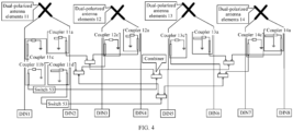
- FIG. 4 and FIG. 5 are schematic structural diagrams of Embodiment 3 of an antenna according to this application.
- this application provides an antenna, including four groups of dual-polarized antenna elements, and each group of dual-polarized antenna elements is connected to two radio frequency interfaces.
- the dual-polarized antenna elements 11 are connected to radio frequency interfaces DIN1 and DIN2
- the dual-polarized antenna elements 12 are connected to radio frequency interfaces DIN3 and DIN4
- the dual-polarized antenna elements 13 are connected to radio frequency interfaces DIN5 and DIN6
- the dual-polarized antenna elements 14 are connected to radio frequency interfaces DIN7 and DIN8.
- At least two couplers are disposed on a calibration signal circuit between two radio frequency interfaces of each group of dual-polarized antenna elements.
- four couplers 11a, 11b, 11c, and 11d are disposed on a calibration signal circuit between the radio frequency interfaces DIN1 and DIN2
- two couplers 12a and 12c are disposed on a calibration signal circuit between the radio frequency interfaces DIN3 and DIN4
- two couplers 13a and 13c are disposed on a calibration signal circuit between the radio frequency interfaces DIN5 and DIN6
- two couplers 14a and 14c are disposed on a calibration signal circuit between the radio frequency interfaces DIN7 and DIN8. Effects of the couplers are classified into two types.
- the switch 53 is disposed on the calibration signal circuit, and the switch 53 has three implementations. To be specific, when the switch is a space switch, the space switch first turns off the calibration signal circuit to obtain the signal on the main feed circuit, then connects to the calibration signal circuit to obtain a mixed signal of the calibration signal and the signal on the main feed circuit, and finally isolates the calibration signal from the signal on the main feed circuit by using the mixed signal and the signal on the main feed circuit.
- the time switch isolates the calibration signal from the signal on the main feed circuit by increasing a delay of the calibration signal.
- the switch is a frequency switch
- the frequency switch isolates the calibration signal from the signal on the main feed circuit by changing a frequency of the calibration signal.
- two radio frequency channels connected to the first interfaces are calibrated as an example, and DIN1 is the second interface.
- the calibration signal is received by DIN2, and a calibration signal circuit through which the calibration signal passes includes A2+C2+CC+A1.
- the calibration signal is coupled to C2 by the coupler 11a after passing through A2, is coupled to A1 by the coupler 11b after passing through the combiner and then passing through CC, and finally reaches DIN1.
- the signal on the main feed circuit is received by DIN2, and a main feed circuit through which the signal on the main feed circuit passes includes A2+B2+U2+B 1+A1.
- the signal on the main feed circuit continues to pass upward through B2 after passing through A2, and then reaches DIN1 along B1 and A1 after passing through the dual-polarized antenna elements 11 (namely, U2).
- the calibration signal is received by DIN4, and a calibration signal circuit through which the calibration signal passes includes A4+C4+CC+A1.
- the calibration signal is coupled to C4 by the coupler 12a after passing through A4, is coupled to A1 by the coupler 11b after passing through the combiner and then passing through CC, and finally reaches DIN1.
- the signal on the main feed circuit is received by DIN4, and a main feed circuit through which the signal on the main feed circuit passes includes A4+B4+U4+U2+B1+A1.
- the signal on the main feed circuit continues to pass upward through B4 after passing through A4, and then reaches DIN1 along B1 and A1 after passing through the dual-polarized antenna elements 12 (namely, U4) and 11 (namely, U2). It can be seen that all the calibration signals sent from DIN2 and DIN4 pass through CC. Therefore, the switch 53 is disposed at CC. When the switch is a space switch, the space switch first turns off the calibration signal circuit at CC to obtain the signal on the main feed circuit, then connects to the calibration signal circuit at CC to obtain a mixed signal of the calibration signal and the signal on the main feed circuit, and finally removes the signal on the main feed circuit from the mixed signal, to obtain the calibration signal.
- the switch when the switch is a time switch, the time switch isolates the calibration signal from the signal on the main feed circuit by increasing a delay of the calibration signal, so that the calibration signal reaches DIN1 late.
- the switch when the switch is a frequency switch, the frequency switch isolates the calibration signal from the signal on the main feed circuit by changing a frequency of the calibration signal, so that the calibration signal and the signal on the main feed circuit can be easily distinguished from the signal received from DIN1.
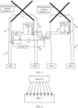
- FIG. 6 and FIG. 7 are two schematic structural diagrams of an embodiment of a base station according to this application.
- the base station includes an antenna 0 and an RRU 6, and the antenna 0 may use the structure shown in any one of the embodiments in FIG. 1 to FIG. 5 .
- the RRU 6 has a total of eight radio frequency interfaces (61 to 68).
- the radio frequency interface 64 may be connected to a radio frequency interface (as a second interface) in the antenna 0 to receive calibration signals from the radio frequency interfaces 65 to 68 (respectively connected to four radio frequency interfaces (as first interfaces) in the antenna 0) and separately calibrate phases and amplitudes of the radio frequency interfaces 65 to 68 based on statuses of the calibration signals received by the radio frequency interface 64, so that the phases and the amplitudes of the radio frequency interfaces 65 to 68 are kept consistent.
- the radio frequency interface 65 may be connected to a radio frequency interface (as a second interface) in the antenna 0 to receive calibration signals from the radio frequency interfaces 61 to 64 (respectively connected to four radio frequency interfaces (as first interfaces) in the antenna 0) and separately calibrate phases and amplitudes of the radio frequency interfaces 61 to 64 based on statuses of the calibration signals received by the radio frequency interface 65, so that the phases and the amplitudes of the radio frequency interfaces 61 to 64 are kept consistent. As shown in FIG. 7 , when there are two RRUs 6 (an RRU 6a and an RRU 6b), each RRU has four radio frequency interfaces (61 to 64).
- the radio frequency interface 64 of the RRU 6a may be connected to a radio frequency interface (as a second interface) in the antenna 0 to receive calibration signals from the radio frequency interfaces 61 to 64 (respectively connected to four radio frequency interfaces (as first interfaces) in the antenna 0) of the RRU 6b and separately calibrate phases and amplitudes of the radio frequency interfaces 61 to 64 of the RRU 6b based on statuses of the calibration signals received by the radio frequency interface 64 of the RRU 6a, so that the phases and the amplitudes of the radio frequency interfaces 61 to 64 are kept consistent.
- the radio frequency interface 61 on the RRU 6b may be connected to a radio frequency interface (as a second interface) in the antenna 0 to receive calibration signals from the radio frequency interfaces 61 to 64 (respectively connected to four radio frequency interfaces (as first interfaces) in the antenna 0) of the RRU 6a and separately calibrate phases and amplitudes of the radio frequency interfaces 61 to 64 of the RRU 6a based on statuses of the calibration signals received by the radio frequency interface 61 of the RRU 6b, so that the phases and the amplitudes of the radio frequency interfaces 61 to 64 are kept consistent.
- a radio frequency interface used as an example for sending and receiving a signal is not fixed, and may be any existing radio frequency interface between the antenna and the RRU. This is not limited in this application.
- the base station selects one of existing radio frequency channels between the antenna and the RRU to calibrate phases and amplitudes of other radio frequency channels without disposing a dedicated calibration port and channel for the antenna and the RRU, so that interference of the signal on the main feed circuit to the calibration signal is avoided, to obtain accurate calibration compensation information, and no additional installation and connection of a calibration channel are required, to be compatible with various RRU devices.
- FIG. 8 is a flowchart of an embodiment of a radio frequency channel calibration method according to this application. As shown in FIG. 8 , the method in this embodiment may be performed by the base station shown in FIG. 6 or FIG. 7 , and the method may include the following steps.
- Step 101 Transmit, through at least two first channels, a calibration signal to a first interface connected to each of the at least two first channels in an antenna.
- the first channel is a to-be-calibrated radio frequency channel, for example, radio frequency channels respectively connected to the radio frequency interfaces 65 to 68 or the radio frequency interfaces 61 to 64 in FIG. 6 , or for another example, radio frequency channels respectively connected to the radio frequency interfaces 61 to 64 of the RRU 6b or the radio frequency interfaces 61 to 64 of the RRU 6a in FIG. 7 .
- Step 102 Isolate the calibration signal from a signal on a main feed circuit, and transmit the calibration signal to a second interface.
- Step 103 Receive the calibration signal through a second channel connected to the second interface.
- the second channel is a radio frequency channel used as a calibration channel
- a radio frequency interface connected to the second channel in the antenna is the second interface, for example, a radio frequency interface on the antenna connected to the radio frequency interface 64 in FIG. 6 , or a radio frequency interface on the antenna connected to the radio frequency interface 65, or for another example, a radio frequency interface on the antenna connected to the radio frequency interface 61 of RRU6b, or a radio frequency interface on the antenna connected to the radio frequency interface 64 of RRU6a in FIG. 7 .
- the first channel and the second channel may be separately radio frequency channels between different radio frequency interfaces on a same RRU and a radio frequency interface of the antenna, or may be radio frequency channels between radio frequency interfaces on different RRUs and a radio frequency interface of the antenna.
- Step 104 Obtain compensation information for phases and amplitudes of the at least two first channels based on the received calibration signal.
- the base station After receiving the calibration signal corresponding to each first channel, the base station compensates for signals of the radio frequency channels to keep phases and amplitudes of the radio frequency channels consistent.
- radio frequency channels in the antenna are calibrated by using one existing radio frequency channel between the antenna and the RRU, so that phases and amplitudes of the other radio frequency channels are kept consistent, interference of the signal on the main feed circuit to the calibration signal is avoided, to obtain accurate calibration compensation information, and no additional installation and connection of a calibration channel are required, to be compatible with various RRU devices.
- FIG. 9 is a schematic structural diagram of an embodiment of a radio frequency channel calibration apparatus according to this application.
- the apparatus includes a transmission module 31, an isolation module 32, a receiving module 33, and a calibration module 34.
- the transmission module 31 is configured to transmit, through at least two first channels, a calibration signal to a first interface connected to each of the at least two first channels in an antenna.
- the isolation module 32 is configured to isolate the calibration signal from a signal on a main feed circuit, and transmit the calibration signal to a second interface.
- the receiving module 33 is configured to receive the calibration signal through a second channel connected to the second interface.
- the calibration module 34 is configured to obtain compensation information for phases and amplitudes of the at least two first channels based on the received calibration signal.
- the at least two first channels and the second channel are separately radio frequency channels between different radio frequency interfaces on a same RRU and a radio frequency interface of the antenna.
- the at least two first channels and the second channel are separately radio frequency channels between radio frequency interfaces on different RRUs and a radio frequency interface of the antenna.
- the apparatus in this embodiment may be configured to execute the technical solution of the method embodiment shown in FIG. 8 .
- Implementation principles and technical effects thereof are similar, and are not further described herein.
- this application provides a computer-readable storage medium.
- the computer-readable storage medium stores instructions. When run on a computer, the instructions are used to perform the method in the embodiment shown in FIG. 8 .
- this application provides a computer program. When executed by a computer, the computer program is used to perform the method in the embodiment shown in FIG. 8 .
- the program may be stored in a computer-readable storage medium.
- the foregoing storage medium includes any medium that can store program code, such as a ROM, a RAM, a magnetic disk, or an optical disc.
Landscapes
- Engineering & Computer Science (AREA)
- Computer Networks & Wireless Communication (AREA)
- Physics & Mathematics (AREA)
- Electromagnetism (AREA)
- Signal Processing (AREA)
- Radio Transmission System (AREA)
- Mobile Radio Communication Systems (AREA)
Claims (9)
- Antenne comprenant :• au moins trois interfaces radiofréquence (DIN 1, DIN 2, DIN 4) et un réseau d'alimentation (5) disposé parmi les au moins trois interfaces radiofréquence (DIN 1, DIN 2, DIN 4), dans laquelle chacune des au moins trois interfaces radiofréquence (DIN 1, DIN 2, DIN 4) est connectée à un canal radiofréquence (7, 8, 10) entre l'interface radiofréquence (DIN 1, DIN 2, DIN 4) et une unité radio distante, RRU (6), dans laquelle le réseau d'alimentation (5) comprend un circuit d'alimentation principal (52), un circuit de signal d'étalonnage (51) et un commutateur (53), et dans laquelle les au moins trois interfaces radiofréquence (DIN 1, DIN 2, DIN 4) comprennent des premières interfaces (DIN 2, DIN 4) et une seconde interface (DIN 1), dans laquelle les premières interfaces (DIN 2, DIN 4) sont chacune configurées pour recevoir un signal de la RRU (6) et transmettre le signal à une seconde interface (DIN 1) en utilisant le réseau d'alimentation (5), et la seconde interface (DIN 1) est configurée pour envoyer le signal à la RRU (6), dans laquelle la seconde interface (DIN 1) est l'une des au moins trois interfaces radiofréquence (DIN 1, DIN 2, DIN 4), et les premières interfaces (DIN 2, DIN 4) sont chacune l'une des au moins trois interfaces radiofréquence à l'exception de la seconde interface (DIN 1),• au moins trois éléments d'antenne, un premier élément d'antenne connecté à la seconde interface (DIN 1) à travers le circuit d'alimentation principal (52), un second élément d'antenne connecté à une première interface (DIN 2) parmi les premières interfaces à travers le circuit d'alimentation principal (52), et un troisième élément d'antenne connecté à une autre première interface (DIN 4) parmi les premières interfaces à travers le circuit d'alimentation principal (52) ; et• au moins trois coupleurs (11a, 11b, 12a) disposés sur le circuit de signal d'étalonnage (51), dans laquelle :∘ un premier coupleur (11a) parmi les au moins trois coupleurs est configuré pour coupler un signal d'étalonnage de l'une première interface (DIN 2) parmi les premières interfaces (DIN 2, DIN 4) du circuit d'alimentation principal (52) au circuit de signal d'étalonnage (51),∘ un deuxième coupleur (12a) parmi les au moins trois coupleurs est configuré pour coupler un signal d'étalonnage de l'autre première interface (DIN 4) parmi les premières interfaces (DIN 2, DIN 4) du circuit d'alimentation principal (52) au circuit de signal d'étalonnage (51), et∘ un troisième coupleur (11b) parmi les au moins trois coupleurs est configuré pour coupler un signal d'étalonnage du circuit de signal d'étalonnage (51), comprenant le signal d'étalonnage couplé à partir de la première interface (DIN 2) parmi les premières interfaces (DIN 2, DIN 4) au circuit de signal d'étalonnage (51) et le signal d'étalonnage couplé depuis l'autre première interface (DIN 4) parmi les premières interfaces (DIN 2, DIN 4) au circuit de signal d'étalonnage (51), du circuit de signal d'étalonnage (51) au circuit d'alimentation principal (52), et le circuit d'alimentation principal (52) est configuré pour envoyer le signal d'étalonnage, couplé du circuit de signal d'étalonnage (51) au circuit d'alimentation principal (52), à la seconde interface (DIN 1), dans laquelle les premier, deuxième et troisième coupleurs sont des coupleurs différents parmi les au moins trois coupleurs (11a, 11b, 12a) ;dans laquelle le signal d'étalonnage envoyé à la seconde interface (DIN 1) est utilisable pour étalonner une phase et une amplitude de chacun des canaux radiofréquence connectés à la première interface correspondante (DIN 2, DIN 4), etdans laquelle le commutateur est configuré pour isoler le signal d'étalonnage du circuit de signal d'étalonnage (51) en provenance d'un signal principal sur le circuit d'alimentation principal (52) provenant du premier élément d'antenne.
- Antenne selon la revendication 1, dans laquelle le commutateur est disposé sur le circuit d'alimentation principal, entre le premier élément d'antenne et le troisième coupleur.
- Antenne selon la revendication 2, dans laquelle le commutateur isole le signal d'étalonnage du circuit de signal d'étalonnage (51) du signal principal sur le circuit d'alimentation principal en désactivant le commutateur.
- Antenne selon la revendication 1, dans laquelle le commutateur est disposé sur le circuit du signal d'étalonnage.
- Antenne selon la revendication 4, dans laquelle le commutateur est configuré pour isoler le signal d'étalonnage du circuit de signal d'étalonnage (51) du signal principal, de sorte que, lorsque le commutateur est éteint, le signal principal est obtenu à la seconde interface (DIN 1) et, lorsque le commutateur est activé, un signal mixte est obtenu au niveau de la seconde interface (DIN 1), dans laquelle le signal mixte comprend le signal principal et le signal d'étalonnage envoyé à la seconde interface (DIN 1).
- Station de base comprenant l'antenne selon l'une quelconque des revendications 1 à 5, et comprenant une unité radio distante, RRU, connectée à chacune des au moins trois interfaces radiofréquence (DIN1, DIN 2, DIN 4) par l'intermédiaire d'un canal radiofréquence (7, 8, 10), dans laquelle la RRU est la RRU mentionnée dans la revendication 1.
- Procédé d'étalonnage de canal radiofréquence effectué par la station de base selon la revendication 6, dans lequel le procédé comprend les étapes :• de transmission (étape 101), à travers les canaux radiofréquence connectés aux premières interfaces (DIN 2, DIN 4), d'un signal d'étalonnage à l'une première interface (DIN 2) et à l'autre première interface (DIN 4) parmi les premières interfaces (DIN 2, DIN 4) ;• de réception (étape 103) du signal d'étalonnage envoyé à la seconde interface (DIN 1) à travers le canal radiofréquence connecté à la seconde interface (DIN 1) ; et• d'obtention (étape 104) d'informations de compensation pour les phases et les amplitudes de ces canaux radiofréquence connectés aux premières interfaces sur la base du signal d'étalonnage reçu.
- Station de base selon la revendication 6, dans laquelle la station de base est également configurée pour exécuter le procédé selon la revendication 7.
- Support de stockage lisible par ordinateur, dans lequel le support de stockage lisible par ordinateur stocke des instructions qui, lorsqu'elles sont exécutées sur un ordinateur d'une station de base selon la revendication 6, amènent la station de base à exécuter le procédé selon la revendication 7.
Applications Claiming Priority (2)
| Application Number | Priority Date | Filing Date | Title |
|---|---|---|---|
| CN201910094297.5A CN111510229B (zh) | 2019-01-30 | 2019-01-30 | 射频通道的校正方法和装置及天线和基站 |
| PCT/CN2020/072465 WO2020156202A1 (fr) | 2019-01-30 | 2020-01-16 | Procédé et appareil de correction de canal radiofréquence, et station de base |
Publications (3)
| Publication Number | Publication Date |
|---|---|
| EP3905552A1 EP3905552A1 (fr) | 2021-11-03 |
| EP3905552A4 EP3905552A4 (fr) | 2022-02-23 |
| EP3905552B1 true EP3905552B1 (fr) | 2024-07-31 |
Family
ID=71840831
Family Applications (1)
| Application Number | Title | Priority Date | Filing Date |
|---|---|---|---|
| EP20747743.1A Active EP3905552B1 (fr) | 2019-01-30 | 2020-01-16 | Procédé et appareil de correction de canal radiofréquence, et station de base |
Country Status (4)
| Country | Link |
|---|---|
| US (1) | US11784728B2 (fr) |
| EP (1) | EP3905552B1 (fr) |
| CN (1) | CN111510229B (fr) |
| WO (1) | WO2020156202A1 (fr) |
Families Citing this family (9)
| Publication number | Priority date | Publication date | Assignee | Title |
|---|---|---|---|---|
| CN111510229B (zh) * | 2019-01-30 | 2022-12-27 | 华为技术有限公司 | 射频通道的校正方法和装置及天线和基站 |
| US11431422B2 (en) * | 2020-11-05 | 2022-08-30 | Electronics And Telecommunications Research Institute | Calibration method for cooperative transmission of cell-free wireless network, and apparatus therefor |
| CN113190271B (zh) * | 2021-04-07 | 2022-10-14 | 中国电子科技集团公司第二十九研究所 | 一种多个独立系统互联的通道校正的方法 |
| CN116744478A (zh) * | 2022-03-03 | 2023-09-12 | 大唐移动通信设备有限公司 | 一种基于原始基站通道合并的新型基站 |
| CN116780187A (zh) * | 2022-03-07 | 2023-09-19 | 康普技术有限责任公司 | 具有提供改善的列内和/或相邻跨列隔离的校准电路连接的基站天线 |
| US12542368B2 (en) | 2022-07-01 | 2026-02-03 | Samsung Electronics Co., Ltd. | Modem supporting digital pre-distortion, antenna module, and method for operating same |
| CN116545550A (zh) * | 2023-06-20 | 2023-08-04 | 中国联合网络通信集团有限公司 | 一种配置信息生成方法、装置、网络设备及存储介质 |
| WO2025026557A1 (fr) * | 2023-08-03 | 2025-02-06 | Huawei Technologies Co., Ltd. | Dispositifs d'antenne, réseaux d'antennes et systèmes d'antenne |
| CN119865404A (zh) * | 2023-10-19 | 2025-04-22 | 上海华为技术有限公司 | 相位校正方法及通信装置 |
Family Cites Families (28)
| Publication number | Priority date | Publication date | Assignee | Title |
|---|---|---|---|---|
| US6236839B1 (en) * | 1999-09-10 | 2001-05-22 | Utstarcom, Inc. | Method and apparatus for calibrating a smart antenna array |
| JP3444270B2 (ja) * | 2000-05-23 | 2003-09-08 | 日本電気株式会社 | アレーアンテナ受信装置の校正システム |
| JP2002353865A (ja) * | 2001-05-23 | 2002-12-06 | Nec Corp | アレーアンテナ送受信装置及びそのキャリブレーション方法 |
| US8320903B2 (en) * | 2005-09-07 | 2012-11-27 | Samsung Electronics Co., Ltd. | Method and system for calibrating multiple types of base stations in a wireless network |
| EP1791278A1 (fr) * | 2005-11-29 | 2007-05-30 | Interuniversitair Microelektronica Centrum (IMEC) | Procédé et dispositif de calibration pour systèmes MIMO |
| CN100512046C (zh) * | 2006-02-10 | 2009-07-08 | 华为技术有限公司 | 一种在多输入多输出系统中发射通道校正方法 |
| CN101651480B (zh) * | 2008-08-14 | 2013-04-24 | 华为技术有限公司 | 有源天线、基站、刷新幅度和相位的方法及信号处理方法 |
| EP2494703A4 (fr) * | 2009-10-29 | 2014-09-03 | Ericsson Telefon Ab L M | Procédé et agencement dans un système de communication |
| JP5367843B2 (ja) * | 2009-12-16 | 2013-12-11 | 株式会社東芝 | 無線信号処理装置及び無線装置 |
| CN102111202B (zh) * | 2010-02-05 | 2014-05-21 | 电信科学技术研究院 | 一种天线校准的方法及装置 |
| CN102594426B (zh) * | 2012-02-21 | 2014-09-10 | 中兴通讯股份有限公司 | 一种有源天线多收发通道同步校准的装置和方法 |
| US20130260844A1 (en) * | 2012-03-28 | 2013-10-03 | Andrew Llc | Series-connected couplers for active antenna systems |
| WO2014026558A1 (fr) * | 2012-08-14 | 2014-02-20 | 华为技术有限公司 | Procédé et appareil d'étalonnage de canal, et système d'accès |
| WO2014040250A1 (fr) * | 2012-09-13 | 2014-03-20 | Telefonaktiebolaget L M Ericsson (Publ) | Procédé et appareil pour étalonnage d'antennes |
| CN103716075B (zh) * | 2012-09-29 | 2016-12-21 | 华为技术有限公司 | 一种多个射频拉远单元间联合通道校正的方法和装置 |
| CN104244296B (zh) * | 2013-06-13 | 2018-02-06 | 华为技术有限公司 | 多rru间通道校正方法及装置 |
| CN104243055B (zh) * | 2013-06-20 | 2016-06-29 | 华为技术有限公司 | 多天线信道校正的方法、装置和基站系统 |
| EP3066762B1 (fr) * | 2013-11-08 | 2018-02-21 | Telefonaktiebolaget LM Ericsson (publ) | Unité radio avec étalonnage d'antenne parallèle interne |
| US10056685B2 (en) * | 2014-03-06 | 2018-08-21 | Samsung Electronics Co., Ltd. | Antenna array self-calibration |
| CN103997352B (zh) * | 2014-05-14 | 2016-02-24 | 电信科学技术研究院 | 有源天线相关设备、系统及收发校准方法 |
| EP3198755B1 (fr) * | 2014-09-23 | 2020-12-23 | Axell Wireless Ltd. | Mappage automatique et gestion de pim et autres interférences de liaison montante dans des systèmes d'antenne numériques répartis |
| CN106330350B (zh) * | 2015-06-30 | 2019-06-14 | 华为技术有限公司 | 多远程射频单元联合通道校正的方法和相关装置 |
| CN107483125B (zh) * | 2016-06-08 | 2020-06-09 | 大唐移动通信设备有限公司 | 基于lte/lte升级版小区的数据处理方法和系统 |
| CN107547146A (zh) * | 2016-06-29 | 2018-01-05 | 中兴通讯股份有限公司 | 天线校正方法及装置 |
| US11271299B2 (en) * | 2016-07-06 | 2022-03-08 | Telefonaktiebolaget Lm Ericsson (Publ) | Method and arrangement for antenna calibration |
| WO2018137148A1 (fr) * | 2017-01-24 | 2018-08-02 | 华为技术有限公司 | Procédé et dispositif de correction d'antenne |
| US11177567B2 (en) * | 2018-02-23 | 2021-11-16 | Analog Devices Global Unlimited Company | Antenna array calibration systems and methods |
| CN111510229B (zh) * | 2019-01-30 | 2022-12-27 | 华为技术有限公司 | 射频通道的校正方法和装置及天线和基站 |
-
2019
- 2019-01-30 CN CN201910094297.5A patent/CN111510229B/zh active Active
-
2020
- 2020-01-16 EP EP20747743.1A patent/EP3905552B1/fr active Active
- 2020-01-16 WO PCT/CN2020/072465 patent/WO2020156202A1/fr not_active Ceased
-
2021
- 2021-07-29 US US17/388,872 patent/US11784728B2/en active Active
Also Published As
| Publication number | Publication date |
|---|---|
| CN111510229A (zh) | 2020-08-07 |
| WO2020156202A1 (fr) | 2020-08-06 |
| EP3905552A4 (fr) | 2022-02-23 |
| US11784728B2 (en) | 2023-10-10 |
| CN111510229B (zh) | 2022-12-27 |
| US20210391929A1 (en) | 2021-12-16 |
| EP3905552A1 (fr) | 2021-11-03 |
Similar Documents
| Publication | Publication Date | Title |
|---|---|---|
| EP3905552B1 (fr) | Procédé et appareil de correction de canal radiofréquence, et station de base | |
| EP3540959B1 (fr) | Commutateur à voies multiples, système de fréquence radio et dispositif de communication sans fil | |
| US9319124B2 (en) | Apparatus and method for supporting multi-antenna transmission in beamformed wireless communication system | |
| EP2943025B1 (fr) | Dispositifs et procédés de localisation permettant de connecter un port d'alimentation d'antenne d'une station de base et un port d'antenne | |
| EP3540956B1 (fr) | Commutateur à voies multiples, système de fréquence radio et dispositif de communication | |
| US9979447B2 (en) | Radio frequency distribution network for a split beam user specific tilt antenna | |
| EP3565134B1 (fr) | Procédé et dispositif de correction d'antenne | |
| US11129167B2 (en) | Calibrating an array antenna | |
| EP3540969B1 (fr) | Commutateur à voies multiples, système à fréquence radio et dispositif de communication | |
| KR101413507B1 (ko) | 프리코딩 행렬을 획득하기 위한 방법 및 디바이스 | |
| US20160329938A1 (en) | Beamforming training using polarization | |
| US10637545B2 (en) | Spatial separation sub-system for supporting multiple-input/multiple-output operations in distributed antenna systems | |
| EP2903176B1 (fr) | Procédé pour transmettre des données entre un équipement utilisateur et une station de base dans un réseau radio sans fil | |
| US8032080B2 (en) | Wireless communication MIMO system with repeaters | |
| WO2015082008A1 (fr) | Nœud de communication sans fil utilisant une formation de faisceau adaptative à antennes polarisées | |
| WO2018004824A1 (fr) | Procédé permettant de tester une opération de formation de faisceau implicite correcte d'un émetteur-récepteur de signaux de paquets de données radiofréquence (rf) | |
| JP2021524704A (ja) | Mimo無線通信における偏波分割多重化の制御 | |
| CN104601208A (zh) | 自适应双频带mimo wi-fi设备及其操作方法 | |
| EP3678398A1 (fr) | Dispositif de point d'accès et procédé de communication | |
| US10944489B2 (en) | Active antenna system, communication device, calibration method of active antenna system and recording medium | |
| CN112352388A (zh) | 无线电信网络 | |
| US20200395992A1 (en) | Beam control method, base station and user equipment | |
| US12335020B2 (en) | Radio communication apparatus, and radio communication method | |
| EP4262110A1 (fr) | Procédé et système de calibrage d'antennes | |
| AU2010365690B8 (en) | Methods and arrangements for wideband precoding |
Legal Events
| Date | Code | Title | Description |
|---|---|---|---|
| STAA | Information on the status of an ep patent application or granted ep patent |
Free format text: STATUS: THE INTERNATIONAL PUBLICATION HAS BEEN MADE |
|
| PUAI | Public reference made under article 153(3) epc to a published international application that has entered the european phase |
Free format text: ORIGINAL CODE: 0009012 |
|
| STAA | Information on the status of an ep patent application or granted ep patent |
Free format text: STATUS: REQUEST FOR EXAMINATION WAS MADE |
|
| 17P | Request for examination filed |
Effective date: 20210726 |
|
| AK | Designated contracting states |
Kind code of ref document: A1 Designated state(s): AL AT BE BG CH CY CZ DE DK EE ES FI FR GB GR HR HU IE IS IT LI LT LU LV MC MK MT NL NO PL PT RO RS SE SI SK SM TR |
|
| A4 | Supplementary search report drawn up and despatched |
Effective date: 20220121 |
|
| RIC1 | Information provided on ipc code assigned before grant |
Ipc: H01Q 3/26 20060101ALN20220117BHEP Ipc: H04B 17/21 20150101ALI20220117BHEP Ipc: H04B 17/14 20150101AFI20220117BHEP |
|
| DAV | Request for validation of the european patent (deleted) | ||
| DAX | Request for extension of the european patent (deleted) | ||
| REG | Reference to a national code |
Ref country code: DE Ref legal event code: R079 Free format text: PREVIOUS MAIN CLASS: H04B0017120000 Ipc: H04B0017140000 Ref country code: DE Ref legal event code: R079 Ref document number: 602020034885 Country of ref document: DE Free format text: PREVIOUS MAIN CLASS: H04B0017120000 Ipc: H04B0017140000 |
|
| GRAP | Despatch of communication of intention to grant a patent |
Free format text: ORIGINAL CODE: EPIDOSNIGR1 |
|
| STAA | Information on the status of an ep patent application or granted ep patent |
Free format text: STATUS: GRANT OF PATENT IS INTENDED |
|
| RIC1 | Information provided on ipc code assigned before grant |
Ipc: H01Q 3/26 20060101ALN20240123BHEP Ipc: H04B 17/21 20150101ALI20240123BHEP Ipc: H04B 17/14 20150101AFI20240123BHEP |
|
| RIC1 | Information provided on ipc code assigned before grant |
Ipc: H01Q 3/26 20060101ALN20240201BHEP Ipc: H04B 17/21 20150101ALI20240201BHEP Ipc: H04B 17/14 20150101AFI20240201BHEP |
|
| RIC1 | Information provided on ipc code assigned before grant |
Ipc: H01Q 3/26 20060101ALN20240205BHEP Ipc: H04B 17/21 20150101ALI20240205BHEP Ipc: H04B 17/14 20150101AFI20240205BHEP |
|
| INTG | Intention to grant announced |
Effective date: 20240220 |
|
| GRAS | Grant fee paid |
Free format text: ORIGINAL CODE: EPIDOSNIGR3 |
|
| GRAA | (expected) grant |
Free format text: ORIGINAL CODE: 0009210 |
|
| STAA | Information on the status of an ep patent application or granted ep patent |
Free format text: STATUS: THE PATENT HAS BEEN GRANTED |
|
| AK | Designated contracting states |
Kind code of ref document: B1 Designated state(s): AL AT BE BG CH CY CZ DE DK EE ES FI FR GB GR HR HU IE IS IT LI LT LU LV MC MK MT NL NO PL PT RO RS SE SI SK SM TR |
|
| REG | Reference to a national code |
Ref country code: CH Ref legal event code: EP Ref country code: GB Ref legal event code: FG4D |
|
| REG | Reference to a national code |
Ref country code: DE Ref legal event code: R096 Ref document number: 602020034885 Country of ref document: DE |
|
| REG | Reference to a national code |
Ref country code: IE Ref legal event code: FG4D |
|
| REG | Reference to a national code |
Ref country code: LT Ref legal event code: MG9D |
|
| REG | Reference to a national code |
Ref country code: NL Ref legal event code: MP Effective date: 20240731 |
|
| PG25 | Lapsed in a contracting state [announced via postgrant information from national office to epo] |
Ref country code: PT Free format text: LAPSE BECAUSE OF FAILURE TO SUBMIT A TRANSLATION OF THE DESCRIPTION OR TO PAY THE FEE WITHIN THE PRESCRIBED TIME-LIMIT Effective date: 20241202 |
|
| REG | Reference to a national code |
Ref country code: AT Ref legal event code: MK05 Ref document number: 1709498 Country of ref document: AT Kind code of ref document: T Effective date: 20240731 |
|
| PG25 | Lapsed in a contracting state [announced via postgrant information from national office to epo] |
Ref country code: PT Free format text: LAPSE BECAUSE OF FAILURE TO SUBMIT A TRANSLATION OF THE DESCRIPTION OR TO PAY THE FEE WITHIN THE PRESCRIBED TIME-LIMIT Effective date: 20241202 |
|
| PG25 | Lapsed in a contracting state [announced via postgrant information from national office to epo] |
Ref country code: NO Free format text: LAPSE BECAUSE OF FAILURE TO SUBMIT A TRANSLATION OF THE DESCRIPTION OR TO PAY THE FEE WITHIN THE PRESCRIBED TIME-LIMIT Effective date: 20241031 |
|
| PG25 | Lapsed in a contracting state [announced via postgrant information from national office to epo] |
Ref country code: FI Free format text: LAPSE BECAUSE OF FAILURE TO SUBMIT A TRANSLATION OF THE DESCRIPTION OR TO PAY THE FEE WITHIN THE PRESCRIBED TIME-LIMIT Effective date: 20240731 Ref country code: GR Free format text: LAPSE BECAUSE OF FAILURE TO SUBMIT A TRANSLATION OF THE DESCRIPTION OR TO PAY THE FEE WITHIN THE PRESCRIBED TIME-LIMIT Effective date: 20241101 Ref country code: NL Free format text: LAPSE BECAUSE OF FAILURE TO SUBMIT A TRANSLATION OF THE DESCRIPTION OR TO PAY THE FEE WITHIN THE PRESCRIBED TIME-LIMIT Effective date: 20240731 Ref country code: PL Free format text: LAPSE BECAUSE OF FAILURE TO SUBMIT A TRANSLATION OF THE DESCRIPTION OR TO PAY THE FEE WITHIN THE PRESCRIBED TIME-LIMIT Effective date: 20240731 |
|
| PG25 | Lapsed in a contracting state [announced via postgrant information from national office to epo] |
Ref country code: BG Free format text: LAPSE BECAUSE OF FAILURE TO SUBMIT A TRANSLATION OF THE DESCRIPTION OR TO PAY THE FEE WITHIN THE PRESCRIBED TIME-LIMIT Effective date: 20240731 |
|
| PG25 | Lapsed in a contracting state [announced via postgrant information from national office to epo] |
Ref country code: LV Free format text: LAPSE BECAUSE OF FAILURE TO SUBMIT A TRANSLATION OF THE DESCRIPTION OR TO PAY THE FEE WITHIN THE PRESCRIBED TIME-LIMIT Effective date: 20240731 |
|
| PG25 | Lapsed in a contracting state [announced via postgrant information from national office to epo] |
Ref country code: AT Free format text: LAPSE BECAUSE OF FAILURE TO SUBMIT A TRANSLATION OF THE DESCRIPTION OR TO PAY THE FEE WITHIN THE PRESCRIBED TIME-LIMIT Effective date: 20240731 Ref country code: IS Free format text: LAPSE BECAUSE OF FAILURE TO SUBMIT A TRANSLATION OF THE DESCRIPTION OR TO PAY THE FEE WITHIN THE PRESCRIBED TIME-LIMIT Effective date: 20241130 |
|
| PG25 | Lapsed in a contracting state [announced via postgrant information from national office to epo] |
Ref country code: HR Free format text: LAPSE BECAUSE OF FAILURE TO SUBMIT A TRANSLATION OF THE DESCRIPTION OR TO PAY THE FEE WITHIN THE PRESCRIBED TIME-LIMIT Effective date: 20240731 |
|
| PG25 | Lapsed in a contracting state [announced via postgrant information from national office to epo] |
Ref country code: ES Free format text: LAPSE BECAUSE OF FAILURE TO SUBMIT A TRANSLATION OF THE DESCRIPTION OR TO PAY THE FEE WITHIN THE PRESCRIBED TIME-LIMIT Effective date: 20240731 Ref country code: RS Free format text: LAPSE BECAUSE OF FAILURE TO SUBMIT A TRANSLATION OF THE DESCRIPTION OR TO PAY THE FEE WITHIN THE PRESCRIBED TIME-LIMIT Effective date: 20241031 |
|
| PG25 | Lapsed in a contracting state [announced via postgrant information from national office to epo] |
Ref country code: RS Free format text: LAPSE BECAUSE OF FAILURE TO SUBMIT A TRANSLATION OF THE DESCRIPTION OR TO PAY THE FEE WITHIN THE PRESCRIBED TIME-LIMIT Effective date: 20241031 Ref country code: PL Free format text: LAPSE BECAUSE OF FAILURE TO SUBMIT A TRANSLATION OF THE DESCRIPTION OR TO PAY THE FEE WITHIN THE PRESCRIBED TIME-LIMIT Effective date: 20240731 Ref country code: NO Free format text: LAPSE BECAUSE OF FAILURE TO SUBMIT A TRANSLATION OF THE DESCRIPTION OR TO PAY THE FEE WITHIN THE PRESCRIBED TIME-LIMIT Effective date: 20241031 Ref country code: NL Free format text: LAPSE BECAUSE OF FAILURE TO SUBMIT A TRANSLATION OF THE DESCRIPTION OR TO PAY THE FEE WITHIN THE PRESCRIBED TIME-LIMIT Effective date: 20240731 Ref country code: LV Free format text: LAPSE BECAUSE OF FAILURE TO SUBMIT A TRANSLATION OF THE DESCRIPTION OR TO PAY THE FEE WITHIN THE PRESCRIBED TIME-LIMIT Effective date: 20240731 Ref country code: IS Free format text: LAPSE BECAUSE OF FAILURE TO SUBMIT A TRANSLATION OF THE DESCRIPTION OR TO PAY THE FEE WITHIN THE PRESCRIBED TIME-LIMIT Effective date: 20241130 Ref country code: HR Free format text: LAPSE BECAUSE OF FAILURE TO SUBMIT A TRANSLATION OF THE DESCRIPTION OR TO PAY THE FEE WITHIN THE PRESCRIBED TIME-LIMIT Effective date: 20240731 Ref country code: GR Free format text: LAPSE BECAUSE OF FAILURE TO SUBMIT A TRANSLATION OF THE DESCRIPTION OR TO PAY THE FEE WITHIN THE PRESCRIBED TIME-LIMIT Effective date: 20241101 Ref country code: FI Free format text: LAPSE BECAUSE OF FAILURE TO SUBMIT A TRANSLATION OF THE DESCRIPTION OR TO PAY THE FEE WITHIN THE PRESCRIBED TIME-LIMIT Effective date: 20240731 Ref country code: ES Free format text: LAPSE BECAUSE OF FAILURE TO SUBMIT A TRANSLATION OF THE DESCRIPTION OR TO PAY THE FEE WITHIN THE PRESCRIBED TIME-LIMIT Effective date: 20240731 Ref country code: BG Free format text: LAPSE BECAUSE OF FAILURE TO SUBMIT A TRANSLATION OF THE DESCRIPTION OR TO PAY THE FEE WITHIN THE PRESCRIBED TIME-LIMIT Effective date: 20240731 Ref country code: AT Free format text: LAPSE BECAUSE OF FAILURE TO SUBMIT A TRANSLATION OF THE DESCRIPTION OR TO PAY THE FEE WITHIN THE PRESCRIBED TIME-LIMIT Effective date: 20240731 |
|
| PG25 | Lapsed in a contracting state [announced via postgrant information from national office to epo] |
Ref country code: RO Free format text: LAPSE BECAUSE OF FAILURE TO SUBMIT A TRANSLATION OF THE DESCRIPTION OR TO PAY THE FEE WITHIN THE PRESCRIBED TIME-LIMIT Effective date: 20240731 Ref country code: SM Free format text: LAPSE BECAUSE OF FAILURE TO SUBMIT A TRANSLATION OF THE DESCRIPTION OR TO PAY THE FEE WITHIN THE PRESCRIBED TIME-LIMIT Effective date: 20240731 Ref country code: DK Free format text: LAPSE BECAUSE OF FAILURE TO SUBMIT A TRANSLATION OF THE DESCRIPTION OR TO PAY THE FEE WITHIN THE PRESCRIBED TIME-LIMIT Effective date: 20240731 |
|
| PG25 | Lapsed in a contracting state [announced via postgrant information from national office to epo] |
Ref country code: EE Free format text: LAPSE BECAUSE OF FAILURE TO SUBMIT A TRANSLATION OF THE DESCRIPTION OR TO PAY THE FEE WITHIN THE PRESCRIBED TIME-LIMIT Effective date: 20240731 |
|
| PG25 | Lapsed in a contracting state [announced via postgrant information from national office to epo] |
Ref country code: CZ Free format text: LAPSE BECAUSE OF FAILURE TO SUBMIT A TRANSLATION OF THE DESCRIPTION OR TO PAY THE FEE WITHIN THE PRESCRIBED TIME-LIMIT Effective date: 20240731 |
|
| PG25 | Lapsed in a contracting state [announced via postgrant information from national office to epo] |
Ref country code: SK Free format text: LAPSE BECAUSE OF FAILURE TO SUBMIT A TRANSLATION OF THE DESCRIPTION OR TO PAY THE FEE WITHIN THE PRESCRIBED TIME-LIMIT Effective date: 20240731 Ref country code: IT Free format text: LAPSE BECAUSE OF FAILURE TO SUBMIT A TRANSLATION OF THE DESCRIPTION OR TO PAY THE FEE WITHIN THE PRESCRIBED TIME-LIMIT Effective date: 20240731 |
|
| REG | Reference to a national code |
Ref country code: DE Ref legal event code: R097 Ref document number: 602020034885 Country of ref document: DE |
|
| PLBE | No opposition filed within time limit |
Free format text: ORIGINAL CODE: 0009261 |
|
| STAA | Information on the status of an ep patent application or granted ep patent |
Free format text: STATUS: NO OPPOSITION FILED WITHIN TIME LIMIT |
|
| 26N | No opposition filed |
Effective date: 20250501 |
|
| REG | Reference to a national code |
Ref country code: CH Ref legal event code: PL |
|
| PG25 | Lapsed in a contracting state [announced via postgrant information from national office to epo] |
Ref country code: SE Free format text: LAPSE BECAUSE OF FAILURE TO SUBMIT A TRANSLATION OF THE DESCRIPTION OR TO PAY THE FEE WITHIN THE PRESCRIBED TIME-LIMIT Effective date: 20240731 |
|
| PG25 | Lapsed in a contracting state [announced via postgrant information from national office to epo] |
Ref country code: LU Free format text: LAPSE BECAUSE OF NON-PAYMENT OF DUE FEES Effective date: 20250116 Ref country code: MC Free format text: LAPSE BECAUSE OF FAILURE TO SUBMIT A TRANSLATION OF THE DESCRIPTION OR TO PAY THE FEE WITHIN THE PRESCRIBED TIME-LIMIT Effective date: 20240731 |
|
| PG25 | Lapsed in a contracting state [announced via postgrant information from national office to epo] |
Ref country code: BE Free format text: LAPSE BECAUSE OF NON-PAYMENT OF DUE FEES Effective date: 20250131 |
|
| PG25 | Lapsed in a contracting state [announced via postgrant information from national office to epo] |
Ref country code: FR Free format text: LAPSE BECAUSE OF NON-PAYMENT OF DUE FEES Effective date: 20250131 |
|
| PG25 | Lapsed in a contracting state [announced via postgrant information from national office to epo] |
Ref country code: CH Free format text: LAPSE BECAUSE OF NON-PAYMENT OF DUE FEES Effective date: 20250131 |
|
| REG | Reference to a national code |
Ref country code: BE Ref legal event code: MM Effective date: 20250131 |
|
| PGFP | Annual fee paid to national office [announced via postgrant information from national office to epo] |
Ref country code: GB Payment date: 20251204 Year of fee payment: 7 |
|
| PG25 | Lapsed in a contracting state [announced via postgrant information from national office to epo] |
Ref country code: IE Free format text: LAPSE BECAUSE OF NON-PAYMENT OF DUE FEES Effective date: 20250116 |
|
| PGFP | Annual fee paid to national office [announced via postgrant information from national office to epo] |
Ref country code: DE Payment date: 20251203 Year of fee payment: 7 |